

Page 1
SM1124 Series
NIPPON PRECISION CIRCUITS INC.
OVERVIEW
The SM1124 Series are melody pager multi-melody
ICs fabricated in NPC’s Molybdenum-gate CMOS.
A maximum of 16 tunes can be stored in
programmable ROM, and the Molybdenum-gate
CMOS process realizes small-sized packages and
low power dissipation.
FEATURES
■
Maximum of 16 tune selections (with up to 512
steps)
■
Level hold playback mode
■
External reference clock input. The frequency can
be selected from the following 12 settings.
• Playback frequency of each song varies (8
frequencies)
- 32.768 kHz system: 32.768 and 65.536 kHz
- 37.5 kHz system: 37.5 and 75.0 kHz
- 38.4 kHz system: 38.4 and 76.8 kHz
- 48.0 kHz system: 48.0 and 96.0 kHz
• Playback frequency of all songs is fixed (4
frequencies)
- 32.768 kHz system: 131.072 kHz
- 37.5 kHz system: 150.0 kHz
- 38.4 kHz system: 153.6 kHz
- 48.0 kHz system: 192.0 kHz
■
2-pin serial data tune selection
■
Power save function
■
External clock gating in non-play mode.
■
2.4 to 3.6 V supply voltage
■
8-pin plastic SOP package
■
Molybdenum-gate CMOS process
Multimelody IC for Pagers
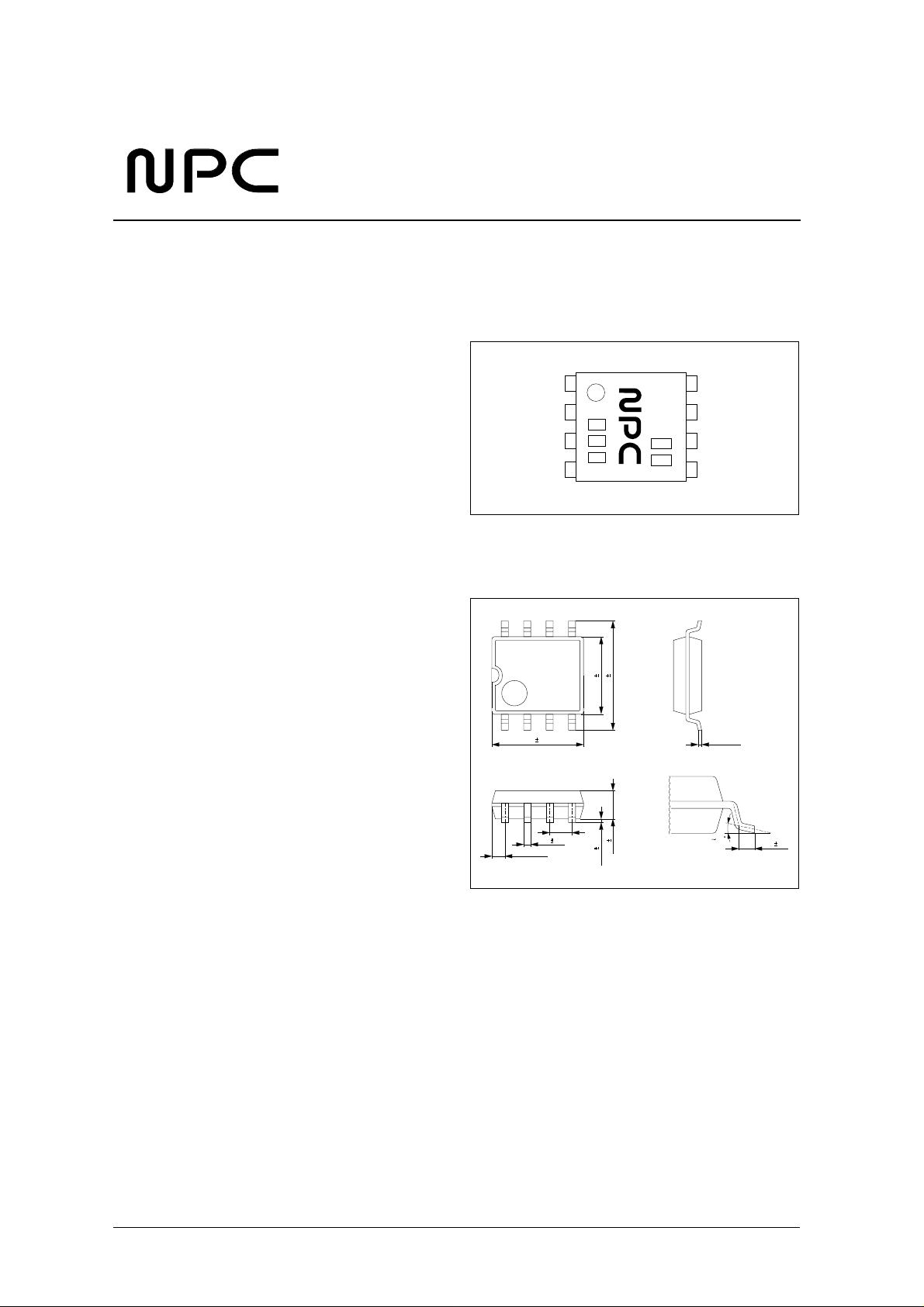
PINOUT
8-pin SOP
SI
SC
ST
0.4 0.1
1.27
1
4
4.4 0.2
6.2 0.3
1.5 0.1
0.05 0.05
124
CLK
PACKAGE DIMENSIONS
Unit: mm
5.2 0.3
0.695TYP
8
VSS
VDD
MTO
5
TEST
+ 0.10
0.15
− 0.05
010
0.4 0.2
NIPPON PRECISION CIRCUITS—1
Page 2
−
−
−
°
°
BLOCK DIAGRAM
SM1124 Series
CLK*
SI*
SC*
ST*
PIN DESCRIPTION
Gate
1/2 or 1/4 SW
Divider
1/128
Control
Circuit
Tempo
Latch
Tempo
Counter
*: Built-in Schmmit-Triger Circuit.
Rhythm
Counter
Scale
Counter
Scale
ROM
Main
ROM
Multi-
plexer
Address
Counter
Start
Address
Latch
VSS
VDD
MTO
TEST
Number Name I/O Function
1 CLK I External reference clock input (Schmitt-trigger circuit and gate circuit built-in)
2 SI I Playback control serial interface data input pin
3 SC I Playback control serial interface clock input pin
4 ST I Playback start/stop control signal input pin
1
1
1
5 TEST I Test input pin. Leave open or tie to VSS. (Pull-down resistance built-in)
6 MTO O Playback signal output pin
7 VDD – Supply pin (+)
8 VSS – Ground pin
1. Pins SI, SC and ST have a built-in Schmitt-trigger circuit.
SPECIFICATIONS
Absolute Maximum Ratings
Parameter Symbol Condition Rating Unit
Supply voltage range V
Input voltage range V
Power dissipation P
Storage temperature range T
Soldering temperature T
Soldering time t
DD
IN
D
stg
sld
sld
V
0.3 to 5.0 V
SS
0.2 to V
+ 0.2 V
DD
150 mW
40 to 125
255
10 s
C
C
NIPPON PRECISION CIRCUITS—2
Page 3
−
° C
−
Recommended Operating Conditions
V
= 0 V unless otherwise specified
SS
−
SM1124 Series
Parameter Symbol Condition
Supply voltage V
Operating temperature T
DC Characteristics
T
= − 20 to 70 ° C, V
a
Parameter Symbol Condition
Supply voltage V
Current consumption (1) I
Current consumption (2) I
Input voltage
Hysteresis width V
Input current
Open voltage V
Output voltage
= 0 V, V
SS
DD
min typ max
DD
opr
2.4 – 3.6 V
20 – 70
= 2.4 to 3.6 V unless otherwise specified
min typ max
2.4 3.0 3.6 V
– 25 200 µA
V
0.2 – V
DD
V
SS
0.2 1.0 – V
– – 0.5 µA
– – 0.5 µA
– – 200 µA
0.4 – V
DD
SS
V
V
V
DD
DD1
DD2
V
I
IH1
I
IL1
I
IH2
OPN
OH
OL
Non-playback mode, 25 ° C – – 0.5 µA
Playback mode, MTO pin
open
IH
IL
T
ST, SI, SC and CLK pins
ST, SI, SC and CLK pins,
V
= V
, 25 ° C
IH
DD
ST, SI, SC and CLK pins,
V
= 0 V, 25 ° C
IL
TEST pin, V
= V
IH
DD
TEST pin – – 0.1 V
MTO pin, I
MTO pin, I
= 1 mA V
OH
= 1 mA V
OL
Rating
Rating
–V
–V
SS
SS
Unit
Unit
DD
+ 0.2 V
DD
+ 0.4 V
V
V
AC Characteristics
T
= − 20 to 70 ° C, V
a
Parameter Symbol Condition
CLK pulse cycle t
CLK HIGH-level pulsewidth t
CLK LOW-level pulsewidth t
SC pulsewidth t
SC HIGH-level pulsewidth t
SC L OW-level pulsewidth t
SI-SC setup time t
SI-SC hold time t
= 0 V, V
SS
DD
= 2.4 to 3.6 V unless otherwise specified
min typ max
CLK
CWH
CWL
SC
SWH
SWL
DS
DH
“CLK input clock” timing
“SC input clock” timing
“Serial input” timing
5.0 – – µs
2.0 – – µs
2.0 – – µs
5.0 – – µs
2.0 – – µs
2.0 – – µs
2.0 – – µs
2.0 – – µs
Rating
Unit
NIPPON PRECISION CIRCUITS—3
Page 4

CLK input clock
CLK
SC input clock
SC
t
t
SWH
CWH
SM1124 Series
V
IH
0.5V
DD
V
t
CWL
t
CLK
t
SWL
t
SC
IL
V
IH
0.5V
V
IL
DD
Serial input
SC
t
DS
SI
FUNCTIONAL DESCRIPTION
Control Functions
External reference clock
The SM1124 can operate at 12 selectable external
reference clock frequencies. Of these, 8 are
selectable for each tune. When multiple external
clock frequencies are input to a single IC, the clock
must be switched during playback mode. Note that
when the frequency in parentheses is selected, all
tunes can only be played using that single fixed
frequency.
V
IH
0.5V
DD
V
IL
t
DH
V
IH
0.5V
DD
V
IL
The external reference clock input is used at any time
as well as during playback mode. If a clock signal is
input when not in playback mode (when ST is
LOW), the gate circuit switches to cutoff the e xternal
reference clock signal from entering the device,
preventing unwanted current flow.
• 32.768 kHz system: 32.768 kHz, 65.536 kHz,
(131.072 kHz)
• 37.5 kHz system: 37.5 kHz, 75.0 kHz,
(150.0 kHz)
• 38.4 kHz system: 38.4 kHz, 76.8 kHz,
(153.6 kHz)
• 48.0 kHz system: 48.0 kHz, 96.0 kHz,
(192.0 kHz)
NIPPON PRECISION CIRCUITS—4
Page 5

Input during playback mode only
,
ST
CLK
Input during non-playback mode
ST
CLK
SM1124 Series
→
→
→
→
→
→
→
→
→
→
→
→
→
→
→
→
Playback control
The ST pin controls the start of playback. While ST
is HIGH (VDD), the tune is played repeatedly, and
when ST goes LOW (VSS), playback stops. Tunes
are selected by the input serial data on pins SI and
Invalid
Data
SI
SC
ST
MTO
Valid
Data
B3 B2 B1 B0
SC. The final 4 bits form the valid selection data, and
this data is retained even after playback.
If serial data is input during playback, the SM1124
ignores this data and playback continues.
Invalid
Data
,,,,,,,,,,,,,,,,,
* Pin SC should be LOW when either a LOW-to-HIGH or HIGH-to-LOW transition occurs on pin ST.
Serial data selection
1
B3 B2 B1 B0 ST Music selection
LLLLL
LLLHL
LLHLL
LLHHL
LHLLL
LHLHL
LHHLL
LHHHL
H 1st tune
H 2nd tune
H 3rd tune
H 4th tune
H 5th tune
H 6th tune
H 7th tune
H 8th tune
B3 B2 B1 B0 ST Music selection
HLLLL
HLLHL
HLHLL
HLHHL
HHL LL
HHLHL
HHHLL
HHHHL
1. H = VDD level, L = VSS level
NIPPON PRECISION CIRCUITS—5
H 9th tune
H 10th tune
H 11th tune
H 12th tune
H 13th tune
H 14th tune
H 15th tune
H 16th tune
Page 6

SM1124 Series
,
SI
#n1 Data #n2 Data
ST
MTO #n1 Play
#n1 Play #n1 Play
*: Tune plays repeatedly when ST is HIGH, and stops immediately when ST goes LOW.
Playback timing diagrams
Playback start
Playback starts 128 ± 1 SCK clock cycles after ST
goes HIGH.
Invalid
Data
SI
SC
Valid
Data
MSB LSB
#n2 Play
ST
CLK
Internal
Clock
MTO
Playback stop
Playback stops immediately when ST goes LOW.
The IC internal clock also stops, regardless of
whether or not there is a clock input signal on pin
CLK.
ST
CLK
Internal
Clock
128 1 Clock
MTO
,,,,,,,,,,,,,,,
NIPPON PRECISION CIRCUITS—6
Page 7

SM1124 Series
Musical Specifications
Maximum program steps
The mask for the built-in ROM can be programmed
with up to a maximum of 512 steps, where each step
represents either a note (sound pitch and length) or a
rest.
Note length (including rests)
Eight rhythm values for notes (rests) can be
programmed. Also, 2 or more notes can be
programmed as tied notes using a tie.
01234567
Note
Rest
x e e. q e q . q h
Å ä ä . Î ä Î Î î
Pitch and scale
The SM1124 performs uniform interval length
processing to reduce the error at high pitches. This
maintains the relative phase when the frequency
varies from the input value.
The pitch varies with the external reference clock
frequency, as shown in the frequency on the
following page.
The frequency variation from the input frequency is
the sum of the relative error, shown in the frequency
table, plus the pitch error.
(Ex) 38.4 kHz system, A4 note
Relative error: 8.99 cent
Pitch error: − 3.58 cent
Total: +5.41 cent
3 3
3 3
.
Error calculation method:
Output frequency
1200 log
-------------------------------------------------
2
Reference frequency
Output frequency
-------------------------------------------------
log
10
Reference frequency
1200
×
=
3986.3 log
3986.3 log
5.41 cent
---------------------------------------------------------------
Output frequency
-------------------------------------------------
10
Reference frequency
441.379
-------------------
10
440.000
≈
log
10
×
2
×≈
×≈
NIPPON PRECISION CIRCUITS—7
Page 8

Frequency tables
SM1124 Series
Number
(Note) A4 is the following note.
Frequency
divider
1 247 2.49 C3 132.664 D#3 151.822 D#3 155.466 G3 194.332
2 233 3.50 C#3 140.635 E3 160.944 E3 164.807 G#3 206.009
3 220 2.89 D3 148.945 F3 170.455 F3 174.545 A3 218.182
4 208 0.00 D#3 157.538 F#3 180.288 F#3 184.615 A#3 230.769
5 196 2.88 E3 167.184 G3 191.327 G3 195.918 B3 244.898
6 185 2.87 F3 177.124 G#3 202.703 G#3 207.568 C4 259.459
7 175
8 165 0.94 G3 198.594 A#3 227.273 A#3 232.727 D 4 290.909
9 156
10 147 0.93 A3 222.912 C4 255.102 C4 261.224 E4 326.531
11 139
12 131 0.42 B3 250.137 D4 286.260 D4 293.130 F#4 366.412
13 124
14 117
15 110 2.89 D4 297.891 F4 340.909 F 4 349.091 A4 436.364
16 104 0.00 D# 4 315.077 F#4 360.577 F#4 369.231 A#4 461.538
17 98 2.88 E4 334.367 G4 382.653 G4 391.837 B4 489.796
18 93
19 87 8.99 F#4 376.644 A4 431.034 A4 441.379 C#5 551.724
20 83
21 78
22 74
23 69 10.29 A#4 474.899 C#5 543.478 C #5 556.522 F5 695.652
24 66
25 62
26 58 10.95 C#5 564.966 E 5 646.552 E5 662.069 G# 5 827.586
27 55 2.89 D5 595.782 F5 681.818 F5 698.182 A5 872.727
28 52 0.00 D#5 630.154 F#5 721.154 F#5 738.462 A #5 923.077
29 49 2.88 E5 668.735 G5 765.306 G5 783.673 B5 979.592
30 46 12.26 F5 712.348 G#5 815.217 G#5 834.783 C6 1043.478
31 44
32 41 11.47 G5 799.220 A#5 914.634 A#5 936.585 D 6 1170.732
33 39
34 37
35 35
36 33
37 31
38 29 10.95 C#6 1129.931 E 6 1293.103 E6 1324.138 G#6 1655.172
39 28
40 26 0.00 D #6 1260.308 F#6 1442.308 F#6 1476.923 A#6 1846.154
41 25
42 23 12.26 F6 1424.696 G#6 1630.435 G #6 1669.565 C7 2086.957
43 22
44 21
ú
&
===
Relative
error
(cent)
0.93 F#3 187.246 A3 214.286 A3 219.429 C#4 274.286
1.96 G#3 210.051 B3 240.385 B 3 246.154 D# 4 307.692
2.21 A#3 235.741 C#4 269.784 C#4 276.259 F4 345.324
4.50 C4 264.258 D# 4 302.419 D#4 309.677 G4 387.097
3.91 C #4 280.068 E 4 320.513 E4 328.205 G# 4 410.256
6.46 F4 352.344 G#4 403.226 G#4 412.903 C5 516.129
9.52 G4 394.795 A#4 451.807 A#4 462.651 D 5 578.313
1.96 G#4 420.103 B4 480.769 B 4 492.308 D# 5 615.385
10.81 A4 442.811 C5 506.757 C5 518.919 E5 648.649
12.74 B4 496.485 D5 568.182 D5 581.818 F#5 727.273
4.50 C5 528.516 D# 5 604.839 D#5 619.355 G5 774.194
10.79 F#5 744.727 A5 852.273 A 5 872.727 C# 6 1090.909
1.96 G#5 840.205 B5 961.538 B5 984.615 D#6 1230.769
10.81 A5 885.622 C6 1013.514 C6 1037.838 E 6 1297.297
14.62 A#5 936.229 C #6 1071.429 C# 6 1097.143 F6 1371.429
12.74 B5 992.970 D6 1136.364 D6 1163.636 F#6 1454.545
4.50 C6 1057.032 D#6 1209.677 D#6 1238.710 G6 1548.387
28.30 D 6 1170.286 F6 1339.286 F6 1371.429 A6 1714.286
32.09 E6 1310.720 G6 1500.000 G6 1536.000 B6 1920.000
10.79 F#6 1489.455 A6 1704.545 A6 1745.455 C# 7 2181.818
30.25 G6 1560.381 A#6 1785.714 A#6 1828.571 D7 2285.714
A4 (440Hz)
32.768 kHz
system
Frequency
Pitch
+21.84 cent pitch
(Hz)
error
37.5 kHz system 38.4 kHz system 48 kHz system
Frequency
Pitch
44.64 cent pitch
error
−
−
−
−
−
(Hz)
−
−
−
−
−
−
Pitch
3.58 cent pitch
−
−
−
−
−
−
−
Frequency
(Hz)
error
−
−
−
−
−
−
Pitch
17.26 cent pitch
Frequency
(Hz)
error
Reference
Pitch
frequency
C3 130.8128
C#3 138.5913
D3 146.8325
D#3 155.5635
E3 164.8138
F3 174.6143
F#3 184.9973
G3 195.9978
G#3 207.6525
A3 220.0000
A#3 233.0820
B3 246.9418
C4 261.6255
C#4 277.1825
D4 293.6650
D#4 311.1270
E4 329.6275
F4 349.2285
F#4 369.9945
G4 391.9955
G#4 415.3050
A4 440.0000
A#4 466.1640
B4 493.8835
C5 523.2510
C#5 554.3650
D5 587.3300
D#5 622.2540
E5 659.2550
F5 698.4570
F#5 739.9890
G5 783.9910
G#5 830.6100
A5 880.0000
A#5 932.3280
B5 987.7670
C6 1046.5020
C#6 1108.7300
D6 1174.6600
D#6 1244.5080
E6 1318.5100
F6 1396.9140
F#6 1479.9780
G6 1567.9820
G#6 1661.2200
A6 1760.0000
A#6 1864.6560
B6 1975.5340
C7 2093.0040
C#7 2217.4600
D7 2349.3200
NIPPON PRECISION CIRCUITS—8
Page 9

SM1124 Series
Tempo
There are 29 tempos that can be selected for each
tune. The tempo varies with the external reference
frequency.
Tempo table
RO M 32.768 kHz system 37.5 kHz system 38.4 kHz system 48 kHz system
Code
03 4
04 5 256.0 293.0 300.0 375.0
05 6 213.3 244.1 250.0 312.5
06 7 Presto 182.9 209.3 214.3 267.9
07 8
08 9 142.2
09 10 128.0 146.5 150.0
0A 11
0B 12 106.7 122.1 125.0
0C 13
0D 14 91.4
0E 15 85.3 97.7
0F 16 80.0 91.6 93.8
10 17
11 18 71.1 81.4 83.3
12 19 67.4 77.1 78.9 98.7
13 20
14 21 61.0 69.8 71.4 89.3
15 22
16 23 55.7
17 24 53.3 61.0 62.5 78.1
18 25 51.2
19 26 49.2 56.3
1A 27 47.4 54.3 55.6 69.4
1B 28 45.7 52.3 53.6 67.0
1C 29 44.1 50.5 51.7
1D 30 42.7 48.8 50.0 62.5
1E 31 41.3 47.3 48.4 60.5
1F 32 40.0 45.8 46.9 Largo 58.6
Frequency
divider
Temp
Prestissimo
Allegro
Moderato
Andante
Adagio
Larghetto
Largo
= Temp
320.0
Prestissimo
160.0 Presto 183.1 Presto 187.5 234.4
Allegro
116.4 133.2 136.4 170.5
98.5 Moderato 112.7
Andante
75.3 86.2 88.2 110.3
64.0
Adagio
58.2 66.6 68.2 85.2
Larghetto
Largo
= Temp
366.2
Prestissimo
162.8
Allegro
Moderato
104.6 107.1 133.9
Andante
73.2
Adagio
63.7
Larghetto
58.6 60.0
Largo
= Temp
375.0
Prestissimo
166.7 208.3
Presto
115.4 144.2
Allegro
100.0 125.0
Moderato
75.0 93.8
Andante
65.2 81.5
57.7 72.1
Adagio
Larghetto
468.8
187.5
156.3
117.2
104.2
75.0
64.7
Quarter note ( q ) length = 1536 × tempo counter frequency divider ÷ CLK frequency
(Ex) Tempo code = 1F (divider = 32), CLK frequency = 32.768 kHz
1536 × 32 ÷ 32768 = 1.5 (seconds)
q
q
q
q =
NIPPON PRECISION CIRCUITS—9
Page 10

TYPICAL APPLICATION
Speaker drive with switching circuit
SM1124 Series
VDD
DC-DC
Converter
CPU
VSS
For example
Q1: hfe 100 MIN SP: Impedance 16 Ω MIN
R1: 1.2k Ω
R2, R3: to be decided by sound volume
Speaker drive with Linear amplifier
VDD
DC-DC
Converter
CPU
VSS
1.5V
2.4 to 3.6V
CLK
SI
SC
ST
1.5V
2.4 to 3.6V
CLK
SI
SC
ST
SM1124
VDD
MTO
TEST
SM1124
VDD
MTO
TEST
VSS
VSS
VR1
SP
R2
R3
SW1
R1
Q1
VCC
C1
IN OUT
GND
C2
SP
+
For example
VR1: 10k Ω MIN
(As the output impedance of MTO terminal
is up to 1k Ω MAX, the value above is gi ven
under the condition that output shall be over
C1: to be decided by Input impedance of
amplifier.
C2, SP: to be decided by Output impedance
of amplifier.
90% of supply voltage amplitude. If it is set
below 10k Ω , output amplitude becomes
smaller.)
NIPPON PRECISION CIRCUITS INC. reserves the right to make changes to the products described in this data sheet in order to
improve the design or performance and to supply the best possible products. Nippon Precision Circuits Inc. assumes no responsibility for
the use of any circuits shown in this data sheet, conveys no license under any patent or other rights, and makes no claim that the circuits
are free from patent infringement. Applications for any devices shown in this data sheet are for illustration only and Nippon Precision
Circuits Inc. makes no claim or warr anty that such applications will be suitab le for the use specified without further testing or modification.
The products described in this data sheet are not intended to use for the apparatus which influence human lives due to the failure or
malfunction of the products. Customers are requested to comply with applicable laws and regulations in effect now and hereinafter,
including compliance with export controls on the distribution or dissemination of the products. Customers shall not export, directly or
indirectly, any products without first obtaining required licenses and approvals from appropriate government agencies.
NIPPON PRECISION CIRCUITS INC.
4-3, Fukuzumi 2-chome
NC9503AE 1996.01
NIPPON PRECISION CIRCUITS INC.
Koto-ku, Tokyo 135-8430, Japan
Telephone: 03-3642-6661
Facsimile: 03-3642-6698
NIPPON PRECISION CIRCUITS—10
 Loading...