

Page 1
24
23
22
21
20
19
18
17
16
15
14
13
1
2
3
4
5
6
7
8
9
10
11
12
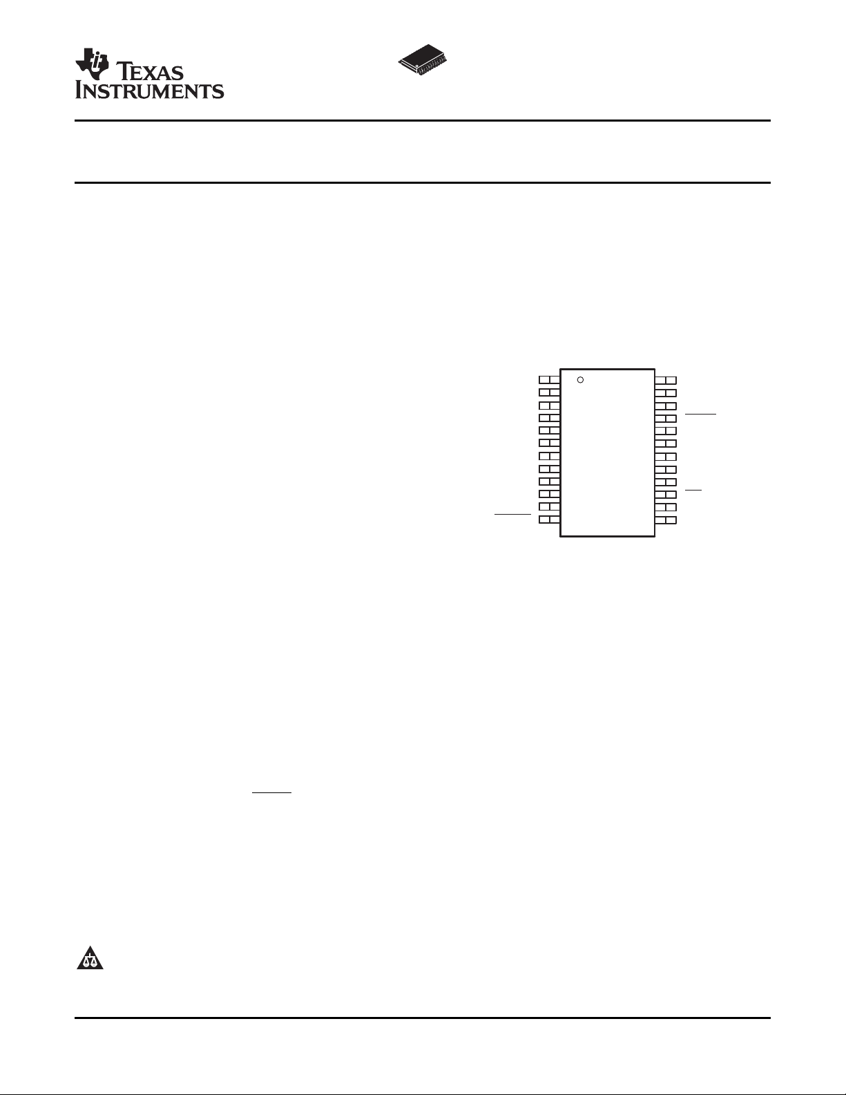
TPS2223A, TPS2224A
DB OR PWP PACKAGE
(TOP VIEW)
5V
5V
DATA
CLOCK
LATCH
NC
12V
†
AVPP
AVCC
AVCC
GND
RESET
5V
NC
NC
SHDN
12V
†
BVPP
BVCC
BVCC
NC
OC
3.3V
3.3V
NC − No internal connection
†
Pin 7 and 20 are NC for TPS2223A.
www.ti.com
CARDBUS POWER-INTERFACE SWITCHES
FOR SERIAL PCMCIA CONTROLLERS
1
FEATURES APPLICATIONS
234
• Provides S-CARD and M-CARD Power
Management for CableCARD™ Applications
• Single-Slot Switch: TPS2220A
Dual-Slot Switches: TPS2223A, TPS2224A,
TPS2226A
• Fast Current Limit Response Time
• Fully Integrated VCC and VPP Switching for
3.3 V, 5 V, and 12 V (no 12 V on TPS2223A)
• Meets Current PC Card™ Standards
• V
• 12-V and 5-V Supplies Can Be Disabled
• TTL-Logic Compatible Inputs
• Short-Circuit and Thermal Protection
• 24-Pin HTSSOP, 24- or 30-Pin SSOP
• 140- µ A (Typical) Quiescent Current from
• Break-Before-Make Switching
• Power-On Reset
• – 40 ° C to 85 ° C Operating Ambient Temperature
Output Selection Independent of V
pp
3.3-V Input
Range
TPS2220A , TPS2223A
TPS2224A , TPS2226A
SLVS428E – MAY 2002 – REVISED MSRCH 2008
• Notebook and Desktop Computers
• Bar Code Scanners
• Digital Cameras
• Set-Top Boxes
• PDAs
CC
DESCRIPTION
The TPS2223A, TPS2224A, and TPS2226A CardBus™ power-interface switches provide an integrated
power-management solution for two PC Card sockets. The TPS2220A is a single-slot option for this family of
devices. These devices allow the controlled distribution of 3.3 V, 5 V, and 12 V to each card slot. The
current-limiting and thermal-protection features eliminate the need for fuses. Current-limit reporting helps the user
isolate a system fault. The switch r
requirements stated in the PC Card specification, and optimized for cost. A faster maximum current limit
response time is the only difference between the TPS2223A, TPS2224A, and TPS2226A and the TPS2223,
TPS2224, and TPS2226.
Like the TPS2214 and TPS2214A and the TPS2216 and TPS2216A, this family of devices supports independent
VPP/VCC switching; however, the standby and interface-mode pins are not supported. Shutdown mode is now
supported independently on SHDN as well as in the serial interface. Optimized for lower power implementation,
the TPS2223A does not support 12-V switching to VPP. For the most current package and ordering information,
see the Package Option Addendum at the end of this document, or see the TI website at www.ti.com .
1
2 CableCARD is a trademark of Cable Tevelision Laboratories, Inc..
3 PC Card, CardBus are trademarks of PCMCIA (Personal Computer Memory Card International Association).
4 All other trademarks are the property of their respective owners.
PRODUCTION DATA information is current as of publication date.
Products conform to specifications per the terms of the Texas
Instruments standard warranty. Production processing does not
necessarily include testing of all parameters.
Please be aware that an important notice concerning availability, standard warranty, and use in critical applications of
Texas Instruments semiconductor products and disclaimers thereto appears at the end of this data sheet.
and current-limit values have been set for the peak and average current
DS(on)
Copyright © 2002 – 2008, Texas Instruments Incorporated
Page 2
www.ti.com
TPS2220A , TPS2223A
TPS2224A , TPS2226A
SLVS428E – MAY 2002 – REVISED MSRCH 2008
These devices have limited built-in ESD protection. The leads should be shorted together or the device placed in conductive foam
during storage or handling to prevent electrostatic damage to the MOS gates.
ABSOLUTE MAXIMUM RATINGS
over operating free-air temperature range (unless otherwise noted)
V
I(3.3V)
V
V
I
T
T
(1) Stresses beyond those listed under "absolute maximum ratings" may cause permanent damage to the device. These are stress ratings
(2) Not applicable for TPS2223A
Input voltage range for card power V
I
I(5V)
(2)
V
I(12V)
Logic input/output voltage – 0.3 to 6 V
V
Output voltage
O
O(xVCC)
V
O(xVPP)
Continuous total power dissipation See Dissipation Rating Table
I
Output current
O
Operating virtual junction temperature range – 40 to 100 ° C
J
Storage temperature range – 55 to 150 ° C
stg
O(xVCC)
I
O(xVPP)
OC sink current 10 mA
only, and functional operation of the device at these or any other conditions beyond those indicated under "recommended operating
conditions" is not implied. Exposure to absolute-maximum-rated conditions for extended periods may affect device reliability.
(1)
TPA222xA UNIT
– 0.3 to 5.5 V
– 0.3 to 5.5 V
– 0.3 to 14 V
– 0.3 to 6 V
– 0.3 to 14 V
Internally Limited
Internally Limited
DISSIPATION RATING TABLE
PACKAGE
DB
(1)
24 890 mW 8.9 mW/ ° C 489 mW 356 mW
30 1095 mW 10.95 mW/ ° C 602 mW 438 mW
PWP 24 3322 mW 33.22 mW/ ° C 1827 mW 1329 mW
(1) These devices are mounted on an JEDEC low-k board (2-oz. traces on surface).
TA≤ 25 ° C DERATING FACTOR TA= 70 ° C TA= 85 ° C
POWER RATING ABOVE TA= 25 ° C POWER RATING POWER RATING
RECOMMENDED OPERATING CONDITIONS
MIN MAX UNIT
(1)
V
Input voltage, V
operations. 5V and 12V are only required for V
I(3.3V)
is required for all circuit
their respective functions.
I
O
f
(clock)
Output current
Clock frequency 2.5 MHz
I(3.3V)
I(5V)
(2)
V
I(12V)
I
at TJ= 100 ° C 1 A
O(xVCC)
I
at TJ= 100 ° C 100 mA
O(xVPP)
Data 200
t
w
Pulse duration ns
Latch 250
Clock 100
Reset 100
t
h
t
su
t
d(latch)
t
d(clock)
(1) It is understood that for V
(2) Not applicable for TPS2223A
Data-to-clock hold time (see Figure 2 ) 100 ns
Data-to-clock setup time (see Figure 2 ) 100 ns
Latch delay time (see Figure 2 ) 100 ns
Clock delay time (see Figure 2 ) 250 ns
< 3 V, voltages within the absolute maximum ratings applied to pin 5V or pin 12V do not damage the IC.
I(3.3V)
2 Submit Documentation Feedback Copyright © 2002 – 2008, Texas Instruments Incorporated
Product Folder Link(s): TPS2220A TPS2223A TPS2224A TPS2226A
3 3.6
3 5.5 V
7 13.5
Page 3
www.ti.com
TPS2220A , TPS2223A
TPS2224A , TPS2226A
SLVS428E – MAY 2002 – REVISED MSRCH 2008
RECOMMENDED OPERATING CONDITIONS (continued)
MIN MAX UNIT
T
J
ELECTRICAL CHARACTERISTICS
TJ= 25 ° C, V
noted)
POWER SWITCH
r
DS(on)
I
OS
T
J
I
I
I
lkg
(1) Pulse-testing techniques maintain junction temperature close to ambient temperature; thermal effects must be taken into account
(2) TPS2223A, TPS2224A, TPS2226A: two switches on. TPS2220A: one switch on.
(3) Specified by design; not tested in production.
(4) From application of short to 110% of final current limit.
Operating virtual junction temperature (maximum to be calculated at worst case PDat 85 ° C
ambient)
= 5 V, V
I(5V)
PARAMETER TEST CONDITIONS
Static drain-source
on-state resistance
Output discharge
resistance
Short-circuit output current
Thermal shutdown
temperature
(2)
Current-limit response time
Input current, quiescent µ A
Leakage current,
output off state
= 3.3 V, V
I(3.3V)
3.3V to xVCC
5V to xVCC
3.3V or 5V to xVPP
12V to xVPP
Discharge at xVCC I
Discharge at xVPP I
= 12 V (not applicable for TPS2223A), all outputs unloaded (unless otherwise
I(12V)
(1)
(2)
IO= 750 mA each 85 110
IO= 750 mA each, TJ= 100 ° C 110 140
(2)
IO= 500 mA each 95 130
IO= 500 mA each, TJ= 100 ° C 120 160
IO= 50 mA each 0.8 1
(2)
IO= 50 mA each, TJ= 100 ° C 1 1.3
(2)
IO= 50 mA each 2 2.5
IO= 50 mA each, TJ= 100 ° C 2.5 3.4
= 1 mA 0.5 0.7 1
O(disc)
= 1 mA 0.2 0.4 0.5
O(disc)
I
Limit (steady-state value), output
powered into a short circuit
Limit (steady-state value), output I
powered into a short circuit,
TJ= 100 ° C
OS(xVCC)
I
OS(xVPP)
OS(xVCC)
I
OS(xVPP)
Thermal trip point Rising temperature 135
Hysteresis 10
(3) (4)
5V to xVCC = 5 V, with 100-m Ω short to GND 10
5V to xVPP = 5 V, with 100-m Ω short to GND 3
I
Normal VO(xVCC) = VO(xVPP) = 3.3 V and
operation also for RESET = 0 V
Shutdown mode I
Shutdown mode µ A
I(3.3V)
I
I(5V)
I
I(12V)
I
I(3.3V)
VO(xVCC) = VO(xVPP) = Hi-z 0.1 2
I(5V)
I
I(12V)
V
= 5 V, V
O(xVCC)
V
= 12 V, V
O(xVPP)
= V
I(5V)
I(5V)
= 0 V
I(12V)
= V
= 0 V
I(12V)
TJ= 100 ° C 50
TJ= 100 ° C 50
– 40 100 ° C
MIN TYP MAX UNIT
1 1.4 2 A
120 200 300 mA
1 1.4 2 A
120 200 300 mA
separately.
m Ω
Ω
k Ω
° C
µ s
140 200
8 12
100 180
0.3 2
0.3 2
10
10
Copyright © 2002 – 2008, Texas Instruments Incorporated Submit Documentation Feedback 3
Product Folder Link(s): TPS2220A TPS2223A TPS2224A TPS2226A
Page 4
www.ti.com
TPS2220A , TPS2223A
TPS2224A , TPS2226A
SLVS428E – MAY 2002 – REVISED MSRCH 2008
ELECTRICAL CHARACTERISTICS (continued)
TJ= 25 ° C, V
noted)
LOGIC SECTION (CLOCK, DATA, LATCH, RESET, SHDN, OC)
I
I
V
IH
V
IL
V
O(sat)
I
lkg
UVLO AND POR (POWER-ON RESET)
V
I(3.3V)
V
hys(3.3V)
V
I(5V)
V
hys(5V)
t
df
V
I(POR)
(5) LATCH has low-current pulldown. RESET and SHDN have low-current pullup.
(6) Specified by design; not tested in production.
= 5 V, V
I(5V)
= 3.3 V, V
I(3.3V)
= 12 V (not applicable for TPS2223A), all outputs unloaded (unless otherwise
I(12V)
PARAMETER TEST CONDITIONS
(5)
I
I(/RESET)
(5)
I
Input current, logic SHDN = 0 V -50 -3 µ A
I(/SHDN)
(5)
I
I(LATCH)
I
I(CLOCK, DATA)
RESET = 5.5 V -1 1
RESET = 0 V -30 -20 -10
SHDN = 5.5 V -1 1
LATCH = 5.5 V 50
LATCH = 0 V -1 1
0 V to 5.5 V -1 1
High-level input voltage, logic 2 V
Low-level input voltage, logic 0.8 V
Output saturation voltage at OC IO= 2 mA 0.14 0.4 V
Leakage current at OC V
O(/OC)
Input voltage at 3.3V pin, UVLO 3.3-V level below which all switches are Hi-Z 2.4 2.7 2.9 V
UVLO hysteresis voltage at VA
(6)
Input voltage at 5V pin, UVLO 5-V level below which only 5V switches are Hi-Z 2.3 2.5 2.8 V
UVLO hysteresis voltage at 5V
Delay time for falling response, UVLO
Input voltage, power-on reset
(6)
(6)
(6)
Delay from voltage hit (step from 3 V to 2.3 V) to
Hi-Z control (90% VGto GND)
3.3-V voltage below which POR is asserted causing a
RESET internally with all line switches open and all 1.7 V
discharge switches closed.
(1)
MIN TYP MAX UNIT
= 5.5 V 0 1 µ A
100 mV
100 mV
4 µ s
4 Submit Documentation Feedback Copyright © 2002 – 2008, Texas Instruments Incorporated
Product Folder Link(s): TPS2220A TPS2223A TPS2224A TPS2226A
Page 5
www.ti.com
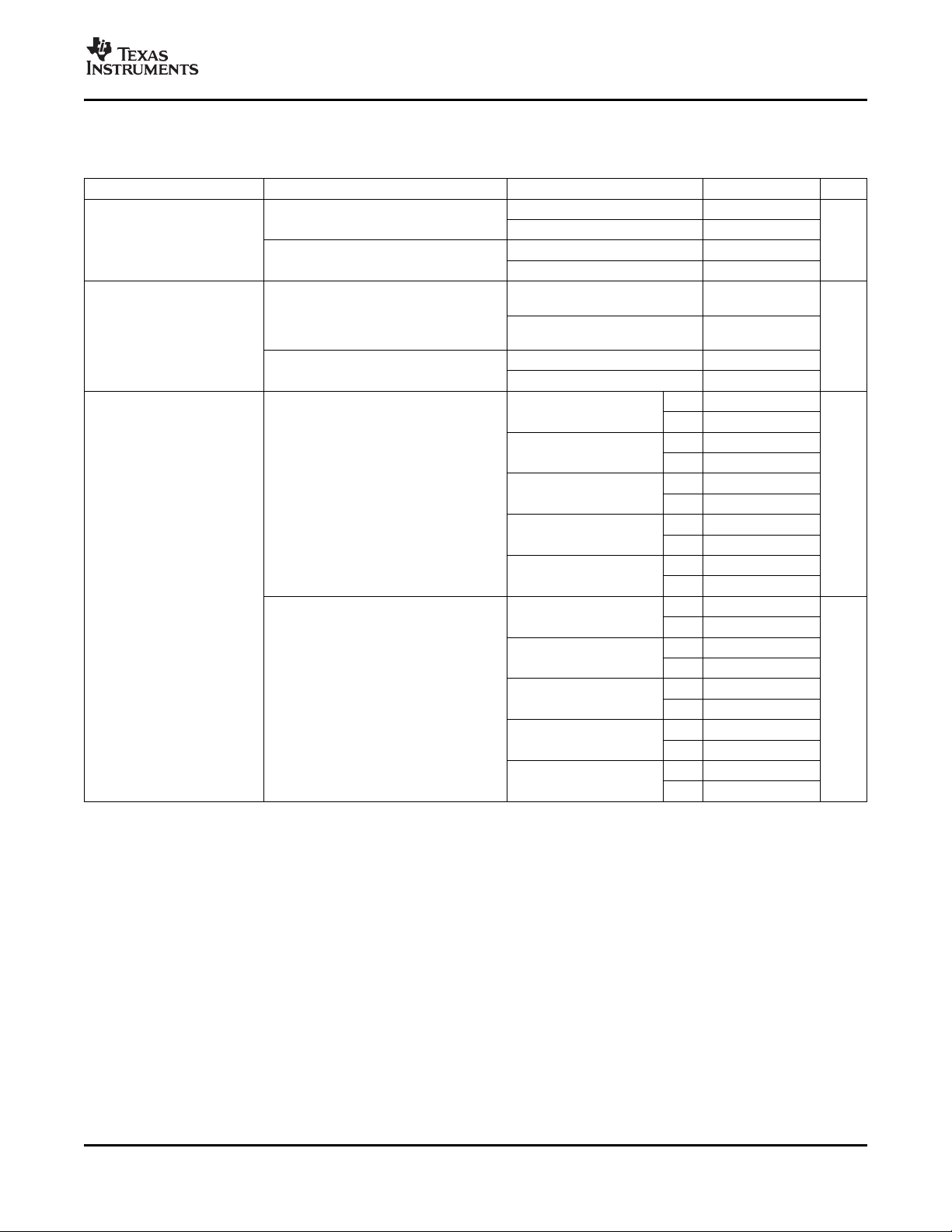
SWITCHING CHARACTERISTICS
V
= 5 V, TA= 25 ° C, V
CC
otherwise noted)
PARAMETER
t
Output rise times
r
t
Output fall times
f
Propagation delay
t
pd
(3)
times
(1) Refer to Parameter Measurement Information in Figure 1 .
(2) No card inserted, assumes a 0.1- µ F output capacitor (see Figure 1 ).
(3) Specified by design; not tested in production.
(4) Not applicable for TPS2223A
(1)
= 3.3 V, V
I(3.3V)
= 5 V, V
I(5V)
= 12 V (not applicable for TPS2223A) all outputs unloaded (unless
I(12)
LOAD CONDITION TEST CONDITIONS
C
I
(3)
C
I
C
I
(3)
C
I
C
I
C
I
= 0.1 µ F, C
L(xVCC)
= 0 A, I
O(xVCC)
L(xVCC)
O(xVCC)
L(xVCC)
O(xVCC)
L(xVCC)
O(xVCC)
L(xVCC)
O(xVCC)
L(xVCC)
O(xVCC)
= 150 µ F, C
= 0.75 A, I
= 0.1 µ F, C
= 0 A, I
= 150 µ F, C
= 0.75 A, I
= 0.1 µ F, C
= 0 A, I
= 150 µ F, C
= 0.75 A, I
O(xVPP)
O(xVPP)
O(xVPP)
= 0.1 µ F,
L(xVPP)
= 0 A
= 10 µ F,
L(xVPP)
= 50 mA
O(xVPP)
= 0.1 µ F,
L(xVPP)
= 0 A
= 10 µ F,
L(xVPP)
= 50 mA
O(xVPP)
= 0.1 µ F,
L(xVPP)
= 0 A
= 10 µ F,
L(xVPP)
= 50 mA
O(xVPP)
TPS2220A , TPS2223A
TPS2224A , TPS2226A
SLVS428E – MAY 2002 – REVISED MSRCH 2008
(2)
V
V
V
V
V
Discharge switches ON
V
Discharge switches ON
V
V
Latch ↑ to xVPP (12V)
= 5 V 0.9
O(xVCC)
= 12 V 0.26
O(xVPP)
= 5 V 1.1
O(xVCC)
= 12 V 0.6
O(xVPP)
= 5 V,
O(xVCC)
= 12 V,
O(xVPP)
= 5 V 2.35
O(xVCC)
= 12 V 3.9
O(xVPP)
(4)
Latch ↑ to xVPP (5V)
Latch ↑ to xVPP (3.3V) ms
Latch ↑ to xVCC (5V)
Latch ↑ to xVCC (3.3V)
Latch ↑ to xVPP (12V)
(4)
Latch ↑ to xVPP (5V)
Latch ↑ to xVPP (3.3V) ms
Latch ↑ to xVCC (5V)
Latch ↑ to xVCC (3.3V)
t
pdon
t
pdoff
t
pdon
t
pdoff
t
pdon
t
pdoff
t
pdon
t
pdoff
t
pdon
t
pdoff
t
pdon
t
pdoff
t
pdon
t
pdoff
t
pdon
t
pdoff
t
pdon
t
pdoff
t
pdon
t
pdoff
MIN TYP MAX UNIT
0.5
0.2
2
0.62
0.77
0.51
0.75
0.52
0.3
2.5
0.3
2.8
2.2
0.8
0.8
0.6
0.8
0.6
0.6
2.5
0.5
2.6
ms
ms
Copyright © 2002 – 2008, Texas Instruments Incorporated Submit Documentation Feedback 5
Product Folder Link(s): TPS2220A TPS2223A TPS2224A TPS2226A
Page 6
www.ti.com
CS
CS
S1
S4
CS
S7
CS
S11
Control Logic
SHDN
RESET
DATA
CLOCK
LATCH
OC
GND
UVLO
POR
Current Limit
Thermal Limit
S2
S5
S3
S6
S8
S9
S10
S12
S13
S14
Discharge
Element
13
14
3.3 V
3.3 V
Power
Inputs
3.3V
1
2
24
5 V
5 V
5 V
Power
Inputs
5V
7
12 V
Power
Inputs
12V
20
12 V
21
12
3
4
5
15
9
10
AVCC
AVCC
17
18
BVCC
BVCC
8
AVPP
19
BVPP
11
Power Outputs
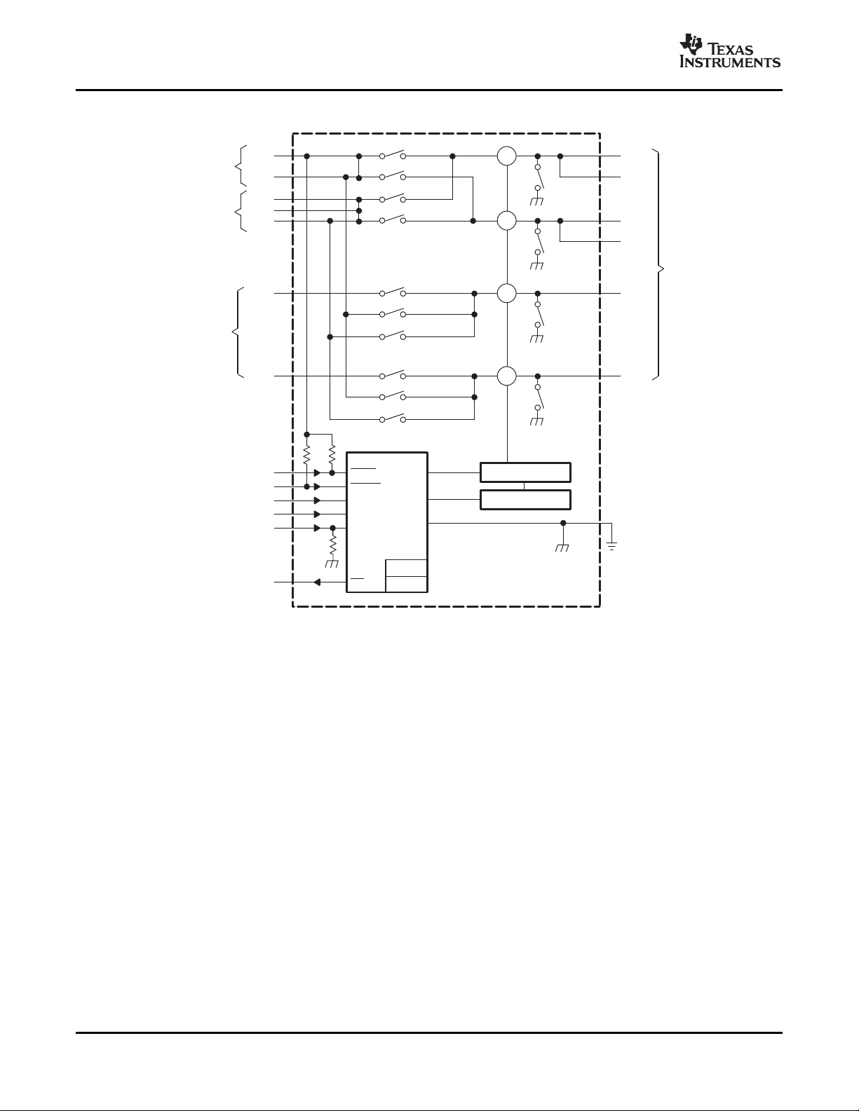
NOTES:A. Diagram shown for 24-pin DB package.
B. Current sense
C. The two 12-V pins must be externally connected.
D. No connections for TPS2223A.
See Note B
See Note B
See Note B
See Note B
See Note C
See Note C
See Note C
See Note D
TPS2220A , TPS2223A
TPS2224A , TPS2226A
SLVS428E – MAY 2002 – REVISED MSRCH 2008
FUNCTIONAL BLOCK DIAGRAM OF TPS2223A, TPS2224A and TPS2226A (see Note A)
6 Submit Documentation Feedback Copyright © 2002 – 2008, Texas Instruments Incorporated
Product Folder Link(s): TPS2220A TPS2223A TPS2224A TPS2226A
Page 7
www.ti.com
See Note A
See Note A
CS
S1
CS
S7
Control Logic
SHDN
RESET
DATA
CLOCK
LATCH
OC
GND
UVLO
POR
Current Limit
Thermal Limit
S2
S3
S4
S5
S6
3.3 V
5 V
5 V
12 V
AVCC
AVCC
AVPP
See Note B
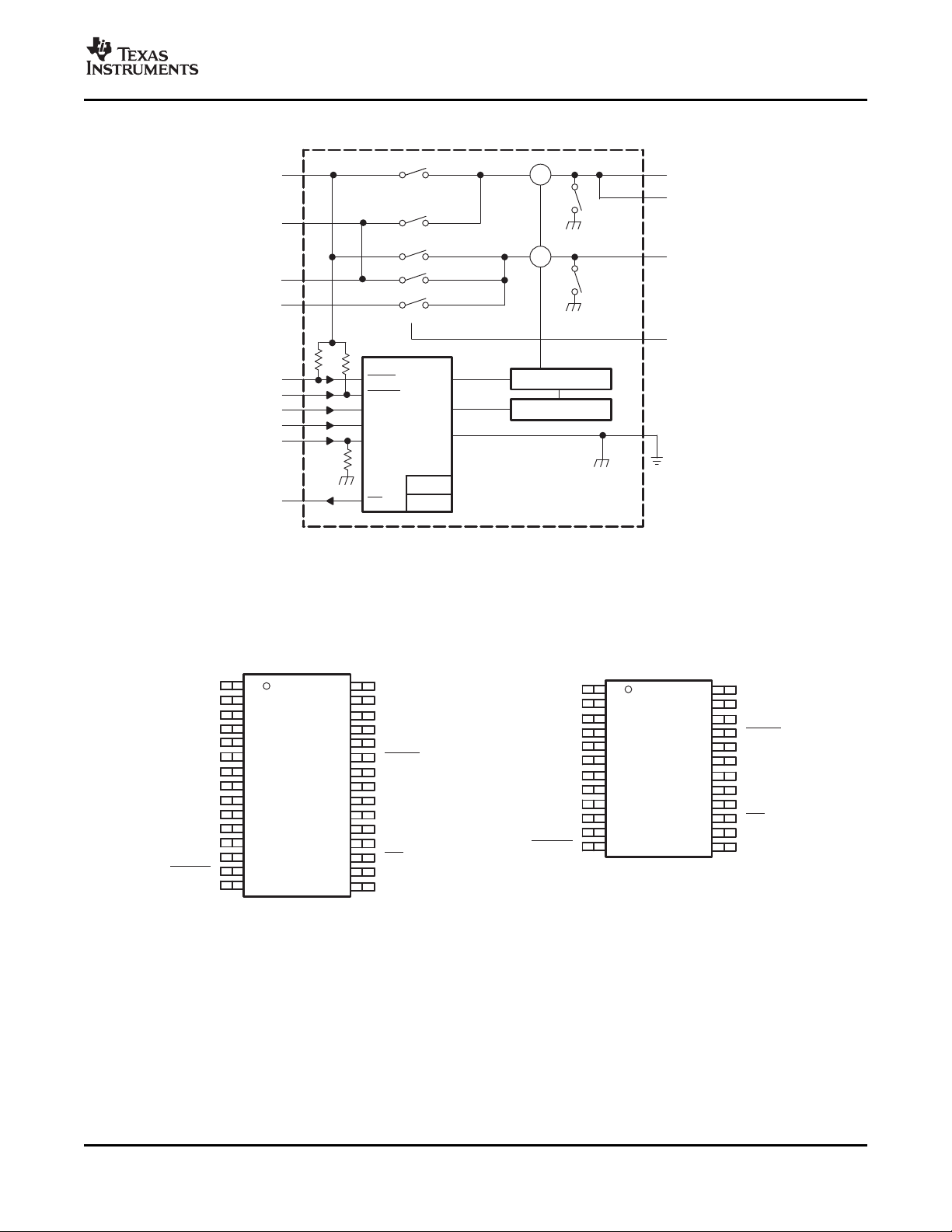
NOTES:A. Current sense
B. The two 12-V pins must be externally connected.
12 V
See Note B
24
23
22
21
20
19
18
17
16
15
14
13
1
2
3
4
5
6
7
8
9
10
11
12
TPS2220A
DB OR PWP PACKAGE
(TOP VIEW)
5V
5V
DATA
CLOCK
LATCH
NC
12V
AVPP
AVCC
AVCC
GND
RESET
NC
NC
NC
SHDN
12V
NC
NC
NC
NC
OC
NC
3.3V
30
29
28
27
26
25
24
23
22
21
20
19
18
17
16
1
2
3
4
5
6
7
8
9
10
11
12
13
14
15
TPS2226A
DB PACKAGE
(TOP VIEW)
5V
5V
DATA
CLOCK
LATCH
NC
12V
AVPP
AVCC
AVCC
AVCC
GND
NC
RESET
3.3V
5V
NC
NC
NC
NC
SHDN
12V
BVPP
BVCC
BVCC
BVCC
NC
OC
3.3V
3.3V
NC - No internal connection
FUNCTIONAL BLOCK DIAGRAM OF TPS2220A
TPS2220A , TPS2223A
TPS2224A , TPS2226A
SLVS428E – MAY 2002 – REVISED MSRCH 2008
Copyright © 2002 – 2008, Texas Instruments Incorporated Submit Documentation Feedback 7
PIN ASSIGNMENTS
Product Folder Link(s): TPS2220A TPS2223A TPS2224A TPS2226A
Page 8
www.ti.com
TPS2220A , TPS2223A
TPS2224A , TPS2226A
SLVS428E – MAY 2002 – REVISED MSRCH 2008
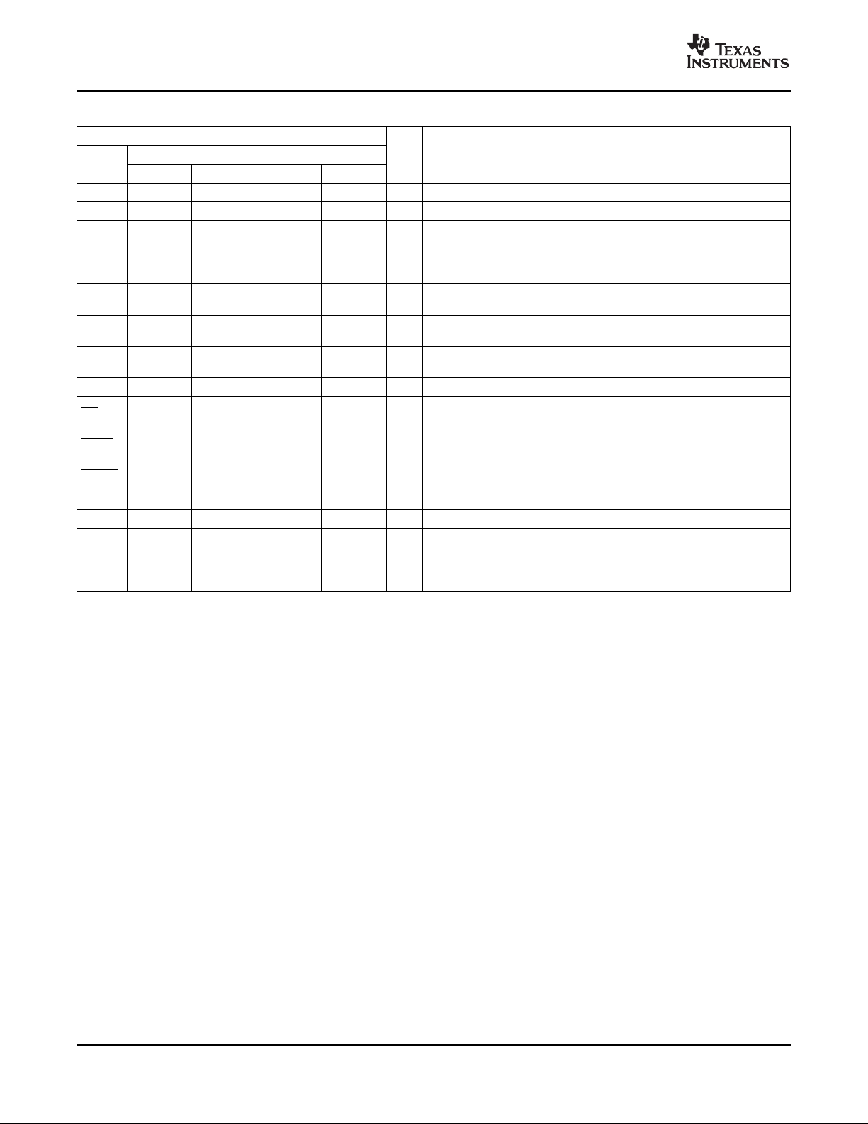
Terminal Functions
TERMINAL
NAME
3.3V 13 13, 14 13, 14 15, 16, 17 I 3.3-V input for card power and chip power
5V 1, 2 1, 2, 24 1, 2, 24 1, 2, 30 I 5-V input for card power
12V 7, 20 NA 7, 20 7, 24 I
AVCC 9, 10 9, 10 9, 10 9, 10, 11 O
AVPP 8 8 8 8 O
BVCC – 17, 18 17, 18 20, 21, 22 O
BVPP – 19 19 23 O
GND 11 11 11 12 Ground
OC 15 15 15 18 O
SHDN 21 21 21 25 I
RESET 12 12 12 14 I
CLOCK 4 4 4 4 I Logic-level clock for serial data word
DATA 3 3 3 3 I Logic-level serial data word
LATCH 5 5 5 5 I Logic-level latch for serial data word, internal pulldown
NC 17, 18, 19, 26, 27, 28, No internal connection
TPS2220A TPS2223A TPS2224A TPS2226A
6, 14, 16, 6, 13, 19,
22, 23, 24 29
6, 7, 16, 6, 16, 22,
20, 22, 23 23
NO. I/O DESCRIPTION
12-V input for card power (xVPP). The two 12-V pins must be
externally connected.
Switched output that delivers 3.3 V, 5 V, ground or high impedance to
card
Switched output that delivers 3.3 V, 5 V, 12 V, ground or high
impedance to card (12 V not applicable to TPS2223A)
Switched output that delivers 3.3 V, 5 V, ground or high impedance to
card
Switched output that delivers 3.3 V, 5 V, 12 V, ground or high
impedance to card (12 V not applicable for TPS2223A)
Open-drain overcurrent reporting output that goes low when an
overcurrent condition exists. An external pullup is required.
Hi-Z (open) all switches. Identical function to serial D8. Asynchronous
active-low command, internal pullup
Logic-level RESET input active low. Asynchronous active-low
command, internal pullup
8 Submit Documentation Feedback Copyright © 2002 – 2008, Texas Instruments Incorporated
Product Folder Link(s): TPS2220A TPS2223A TPS2224A TPS2226A
Page 9
www.ti.com
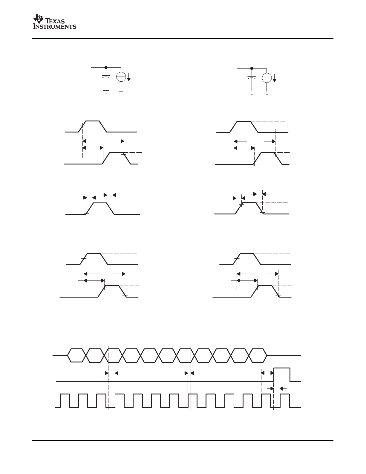
PARAMETER MEASUREMENT INFORMATION
50%
LATCH
V
DD
GND
10%
90%
t
pd(on)
GND
V
O(xVPP)
Propagation Delay (xVPP)
50%
LATCH
V
DD
GND
10%
90%
t
pd(on)
GND
V
O(xVCC)
Propagation Delay (xVCC)
10%
90%
t
r
GND
V
O(xVPP)
Rise/Fall Time (xVPP)
t
f
10%
90%
t
r
GND
V
O(xVCC)
Rise/Fall Time (xVCC)
t
f
50%
V
DD
GND
10%
90%
t
on
GND
V
O(xVCC)
Turnon/off Time (xVCC)
xVPP
VOLTAGE WAVEFORMS
LOAD CIRCUIT (xVPP)
I
O(xVPP)
xVCC
50%
LATCH
V
DD
GND
10%
90%
t
on
GND
V
O(xVPP)
Turnon/off Time (xVPP)
I
O(xVCC)
t
pd(off)
t
pd(off)
t
off
t
off
LOAD CIRCUIT (xVCC)
V
I(12V/5V/3.3V)
V
I(5V/3.3V)
V
I(12V/5V/3.3V)
V
I(5V/3.3V)
V
I(12V/5V/3.3V)
V
I(5V/3.3V)
LATCH
D10
D9
D8 D7
D6
D5
D4 D3
D2
DATA
LATCH
CLOCK
D1
D0
Data Setup Time Data Hold Time Latch Delay Time
Clock Delay Time
TPS2220A , TPS2223A
TPS2224A , TPS2226A
SLVS428E – MAY 2002 – REVISED MSRCH 2008
Figure 1. Test Circuits and Voltage Waveforms
NOTE: Data is clocked in on the positive edge of the clock. The positive edge of the latch signal should occur before the next
Copyright © 2002 – 2008, Texas Instruments Incorporated Submit Documentation Feedback 9
positive edge of the clock. For definition of D0 to D10, see the control logic table.
Figure 2. Serial-Interface Timing for TPS2226A
Product Folder Link(s): TPS2220A TPS2223A TPS2224A TPS2226A
Page 10
www.ti.com
1 2 3 4 5
t − Time − ms
0
V
O(/OC)
2 V/div
I
O(xVPP)
2 A/div
100 200 300 400 500
t − Time − µs
0
V
O(/OC)
5 V/div
I
O(VCC)
5 A/div
V
IN(5V)
2 V/div
TPS2220A , TPS2223A
TPS2224A , TPS2226A
SLVS428E – MAY 2002 – REVISED MSRCH 2008
PARAMETER MEASUREMENT INFORMATION (continued)
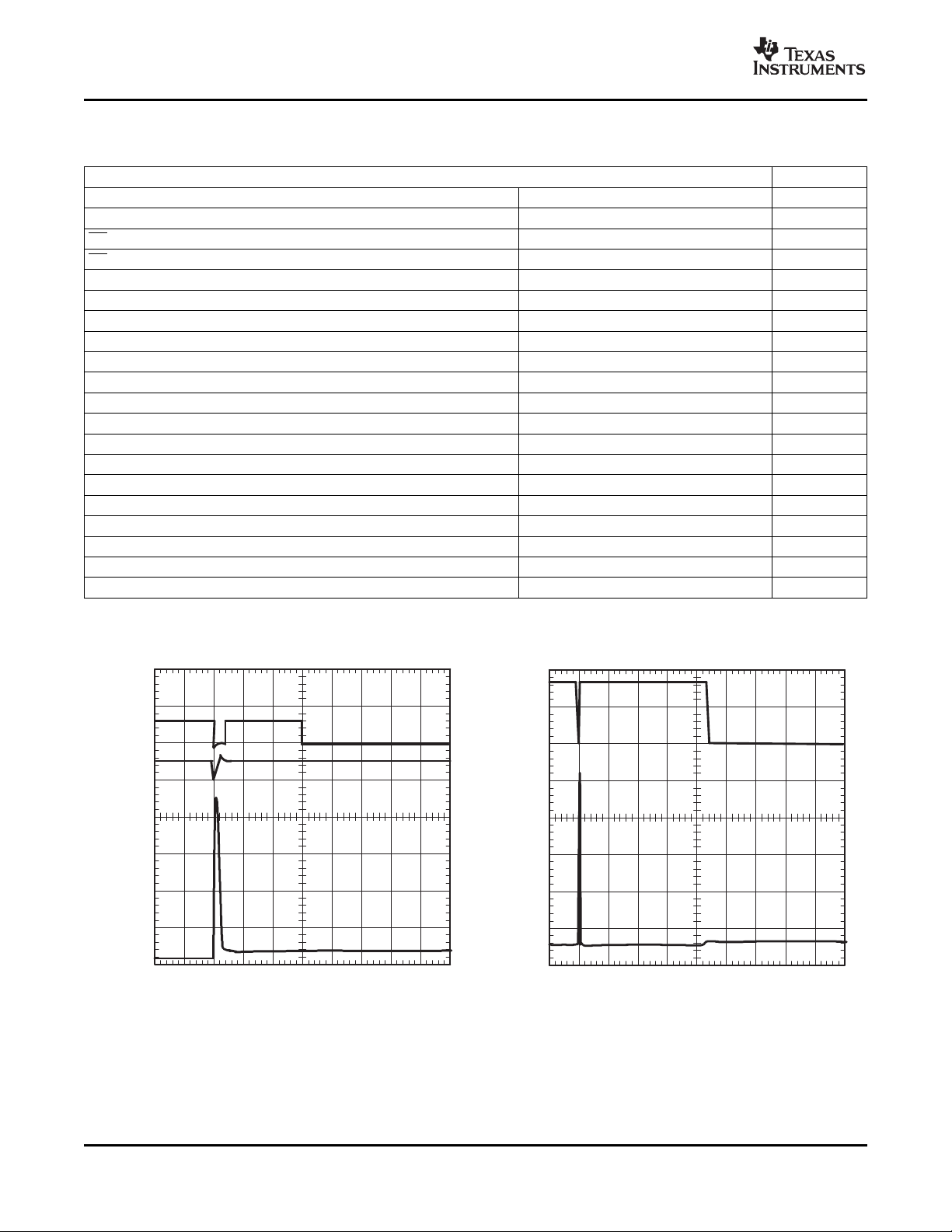
Table of Graphs
Short-circuit response, short applied to powered-on 5-V xVCC-switch output vs Time 3
Short-circuit response, short applied to powered-on 12-V xVPP-switch output vs Time 4
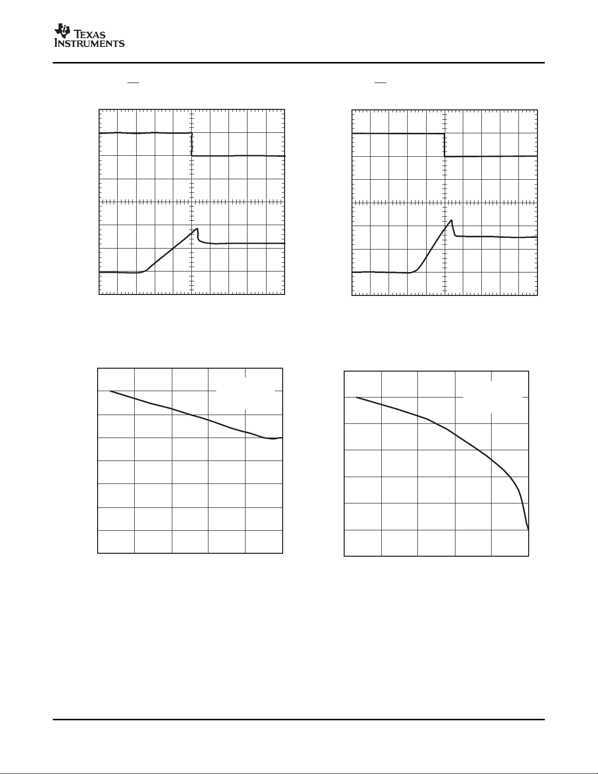
OC response with ramped overcurrent-limit load on 5-V xVCC-switch output vs Time 5
OC response with ramped overcurrent-limit load on 12-V xVPP-switch output vs Time 6
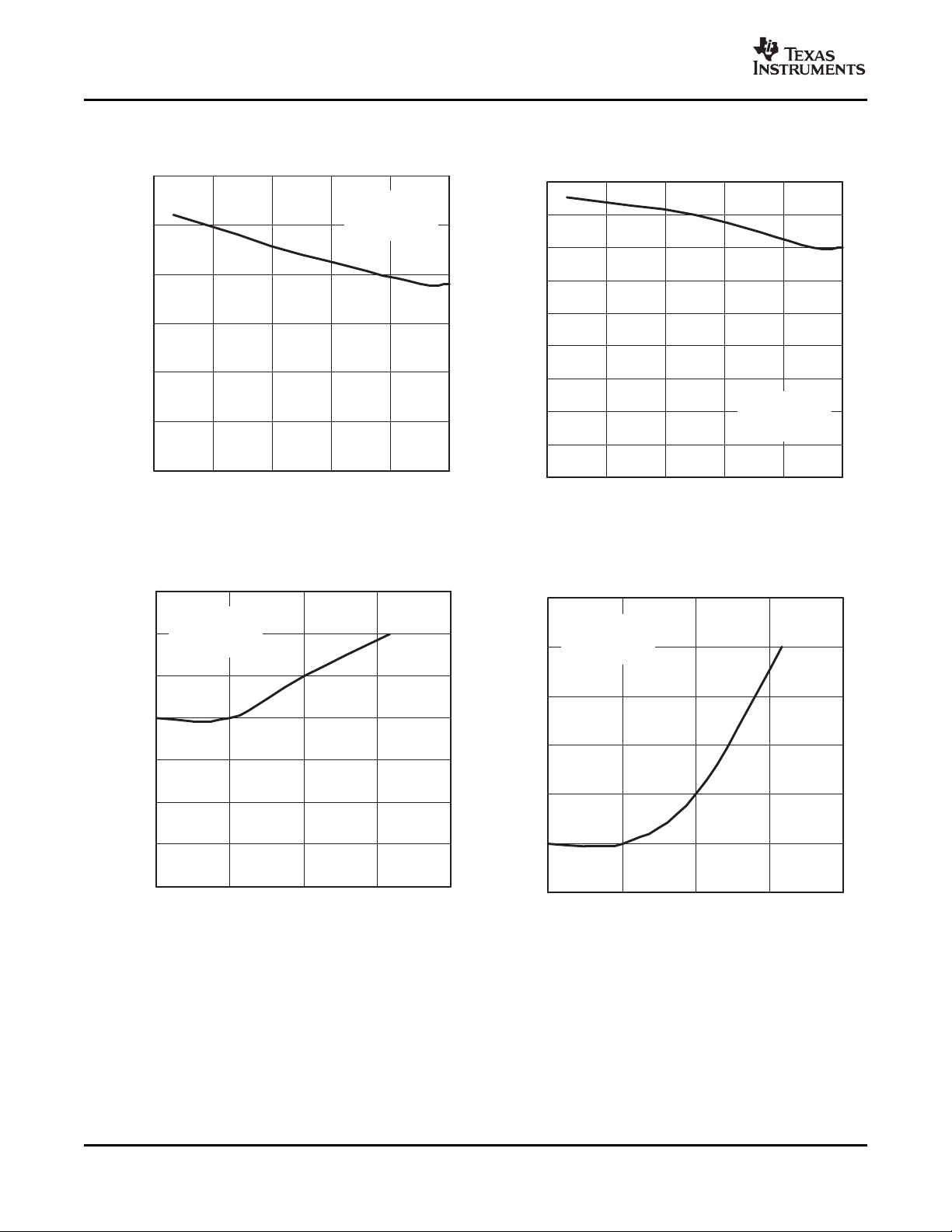
xVCC Turnon propagation delay time
xVCC Turnoff propagation delay time
xVPP Turnon propagation delay time
xVPP Turnoff propagation delay time
xVCC Turnon propagation delay time (T
xVCC Turnoff propagation delay time (T
xVPP Turnon propagation delay time (T
xVPP Turnoff propagation delay time (T
xVCC Rise time
xVCC Fall time
xVPP Rise time
xVPP Fall time
= 150 µ F) vs Junction temperature 15
L
= 150 µ F) vs Junction temperature 16
L
= 10 µ F) vs Junction temperature 17
L
= 10 µ F) vs Junction temperature 18
L
xVCC Rise time (TJ= 25 ° C) vs Load capacitance 19
xVCC Fall time (T
xVPP Rise time (T
xVPP Fall time (T
= 25 ° C) vs Load capacitance 20
J
= 25 ° C) vs Load capacitance 21
J
= 25 ° C) vs Load capacitance 22
J
= 150 µ F) vs Junction temperature 7
L
= 150 µ F) vs Junction temperature 8
L
= 10 µ F) vs Junction temperature 9
L
= 10 µ F) vs Junction temperature 10
L
= 25 ° C) vs Load capacitance 11
J
= 25 ° C) vs Load capacitance 12
J
= 25 ° C) vs Load capacitance 13
J
= 25 ° C) vs Load capacitance 14
J
FIGURE
SHORT-CIRCUIT RESPONSE, SHORT-CIRCUIT RESPONSE,
SHORT APPLIED TO POWERED-ON 5-V SHORT APPLIED TO POWERED-ON 12-V
xVCC-SWITCH OUTPUT xVPP-SWITCH OUTPUT
Figure 3. Figure 4.
10 Submit Documentation Feedback Copyright © 2002 – 2008, Texas Instruments Incorporated
Product Folder Link(s): TPS2220A TPS2223A TPS2224A TPS2226A
Page 11
www.ti.com
10 20 30 40 50
t − Time − ms
0
V
O(/OC)
5 V/div
I
O(xVCC)
1 A/div
2 4 6 8 10
t − Time − ms
0
V
O(/OC)
5 V/div
I
O(xVPP)
100 mA/div
0
0.1
0.2
0.3
0.4
0.5
0.6
0.7
0.8
−50 −20 10 40 70 100
xVCC = 5 V
IO = 0.75 A
C
L
= 150 µF
− Turnon Propagation Delay T ime, xVCC − ms
t
pd(on)
TJ − Junction Temperature − °C
2.25
2.3
2.35
2.4
2.45
2.5
2.55
2.6
−50 −20 10 40 70 100
xVCC = 5 V
IO = 0.75 A
CL = 150 µF
t
pd(off)
TJ − Junction Temperature − °C
− Turnoff Propagation Delay T ime, xVCC − ms
TPS2220A , TPS2223A
TPS2224A , TPS2226A
SLVS428E – MAY 2002 – REVISED MSRCH 2008
OC RESPONSE WITH RAMPED OC RESPONSE WITH RAMPED
OVERCURRENT-LIMIT LOAD ON 5-V OVERCURRENT-LIMIT LOAD ON 12-V
xVCC-SWITCH OUTPUT xVPP-SWITCH OUTPUT
Figure 5. Figure 6.
TURNON PROPAGATION DELAY TIME, xVCC TURNOFF PROPAGATION DELAY TIME, xVCC
vs vs
JUNCTION TEMPERATURE JUNCTION TEMPERATURE
Figure 7. Figure 8.
Copyright © 2002 – 2008, Texas Instruments Incorporated Submit Documentation Feedback 11
Product Folder Link(s): TPS2220A TPS2223A TPS2224A TPS2226A
Page 12
www.ti.com
0
0.5
1
1.5
2
2.5
3
−50 −20 10 40 70 100
t
pd(on)
TJ − Junction Temperature − °C
xVPP = 12 V
IO = 0.05 A
CL = 10 µF
− Turnon Propagation Delay T ime, xVPP − ms
0
0.1
0.2
0.3
0.4
0.5
0.6
0.7
0.8
0.9
−50 −20 10 40 70 100
− Turnoff Propagation Delay T ime, xVCC − ms
t
pd(off)
TJ − Junction Temperature − °C
xVCC = 12 V
IO = 0.05 A
CL = 10 µF
0
0.1
0.2
0.3
0.4
0.5
0.6
0.7
0.1 1 10 100 1000
− Turnon Propagation Delay T ime, xVCC − ms
t
pd(on)
xVCC = 5 V
IO = 0.75 A
TJ = 25°C
CL − Load Capacitance − µF
2.25
2.3
2.35
2.4
2.45
2.5
2.55
0.1 1 10 100 1000
xVCC = 5 V
IO = 0.75 A
TJ = 25°C
CL − Load Capacitance − µF
t
pd(off)
− Turnoff Propagation Delay T ime, xVCC − ms
TPS2220A , TPS2223A
TPS2224A , TPS2226A
SLVS428E – MAY 2002 – REVISED MSRCH 2008
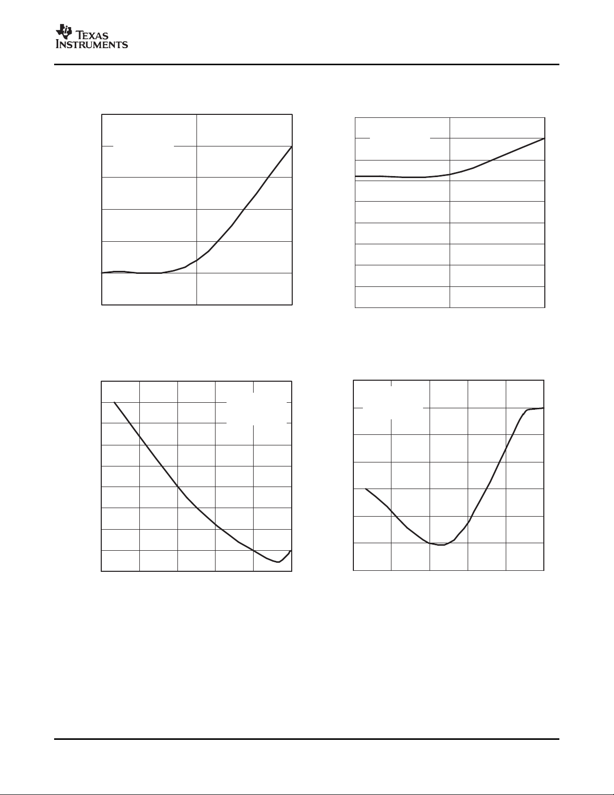
TURNON PROPAGATION DELAY TIME, xVPP TURNON PROPAGATION DELAY TIME, xVPP
JUNCTION TEMPERATURE JUNCTION TEMPERATURE
TURNON PROPAGATION DELAY TIME, xVCC TURNON PROPAGATION DELAY TIME, xVCC
LOAD CAPACITANCE LOAD CAPACITANCE
vs vs
Figure 9. Figure 10.
vs vs
12 Submit Documentation Feedback Copyright © 2002 – 2008, Texas Instruments Incorporated
Figure 11. Figure 12.
Product Folder Link(s): TPS2220A TPS2223A TPS2224A TPS2226A
Page 13
www.ti.com
1.95
2
2.05
2.1
2.15
2.2
2.25
0.1 1 10
− Turnon Propagation Delay T ime, xVPP − ms
t
pd(on)
xVPP = 12 V
IO = 0.05 A
TJ = 25°C
CL − Load Capacitance − µF
0
0.1
0.2
0.3
0.4
0.5
0.6
0.7
0.8
0.9
0.1 1 10
− Turnoff Propagation Delay T ime, xVPP − ms
t
pd(off)
xVPP = 12 V
IO = 0.05 A
TJ = 25°C
CL − Load Capacitance − µF
2.34
2.35
2.36
2.37
2.38
2.39
2.4
2.41
−50 −20 10 40 70 100
− Fall Time xVCC − ms
t
f
TJ − Junction Temperature − °C
xVCC = 5 V
IO = 0.75 A
CL = 150 µF
1.04
1.06
1.08
1.1
1.12
1.14
1.16
1.18
1.2
1.22
−50 −20 10 40 70 100
− Rise Time, xVCC − ms
t
r
TJ − Junction Temperature − °C
xVCC = 5 V
IO = 0.75 A
CL = 150 µF
TPS2220A , TPS2223A
TPS2224A , TPS2226A
SLVS428E – MAY 2002 – REVISED MSRCH 2008
TURNON PROPAGATION DELAY TIME, xVPP TURNON PROPAGATION DELAY TIME, xVPP
LOAD CAPACITANCE LOAD CAPACITANCE
JUNCTION TEMPERATURE JUNCTION TEMPERATURE
vs vs
Figure 13. Figure 14.
RISE TIME, xVCC FALL TIME, xVCC
vs vs
Copyright © 2002 – 2008, Texas Instruments Incorporated Submit Documentation Feedback 13
Figure 15. Figure 16.
Product Folder Link(s): TPS2220A TPS2223A TPS2224A TPS2226A
Page 14
www.ti.com
0.575
0.58
0.585
0.59
0.595
0.6
0.605
−50 −20 10 40 70 100
− Rise Time xVPP − ms
t
r
TJ − Junction Temperature − °C
xVPP = 12 V
IO = 0.05 A
CL = 10 µF
3.85
3.9
3.95
4
4.05
4.1
4.15
−50 −20 10 40 70 100
− Fall Time, xVPP − ms
t
f
TJ − Junction Temperature − °C
xVPP = 12 V
IO = 0.05 A
CL = 10 µF
0
0.5
1
1.5
2
2.5
0.1 1 10 100 1000
− Fall Time xVCC − ms
t
f
xVCC = 5 V
IO = 0.75 A
TJ = 25°C
CL − Load Capacitance − µF
0
0.2
0.4
0.6
0.8
1
1.2
0.1 1 10 100 1000
− Rise Time, xVCC − ms
t
r
xVCC = 5 V
IO = 0.75 A
TJ = 25°C
CL − Load Capacitance − µF
TPS2220A , TPS2223A
TPS2224A , TPS2226A
SLVS428E – MAY 2002 – REVISED MSRCH 2008
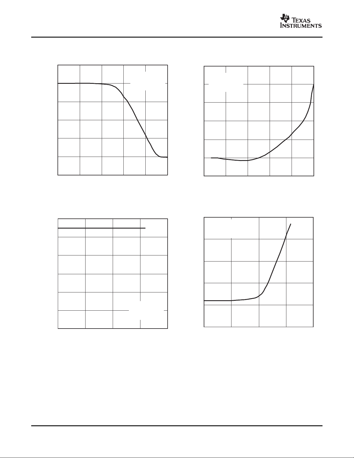
RISE TIME, xVPP FALL TIME, xVPP
JUNCTION TEMPERATURE JUNCTION TEMPERATURE
vs vs
Figure 17. Figure 18.
RISE TIME, xVCC FALL TIME, xVCC
LOAD CAPACITANCE LOAD CAPACITANCE
vs vs
Figure 19. Figure 20.
14 Submit Documentation Feedback Copyright © 2002 – 2008, Texas Instruments Incorporated
Product Folder Link(s): TPS2220A TPS2223A TPS2224A TPS2226A
Page 15
www.ti.com
0
0.5
1
1.5
2
2.5
3
3.5
4
4.5
0.1 1 10
− Fall Time, xVPP − ms
t
f
xVPP = 12 V
IO = 0.05 A
TJ = 25°C
CL − Load Capacitance − µF
0
0.1
0.2
0.3
0.4
0.5
0.6
0.7
0.1 1 10
− Rise Time, xVPP − ms
t
r
xVPP = 12 V
IO = 0.05 A
TJ = 25°C
CL − Load Capacitance − µF
SLVS428E – MAY 2002 – REVISED MSRCH 2008
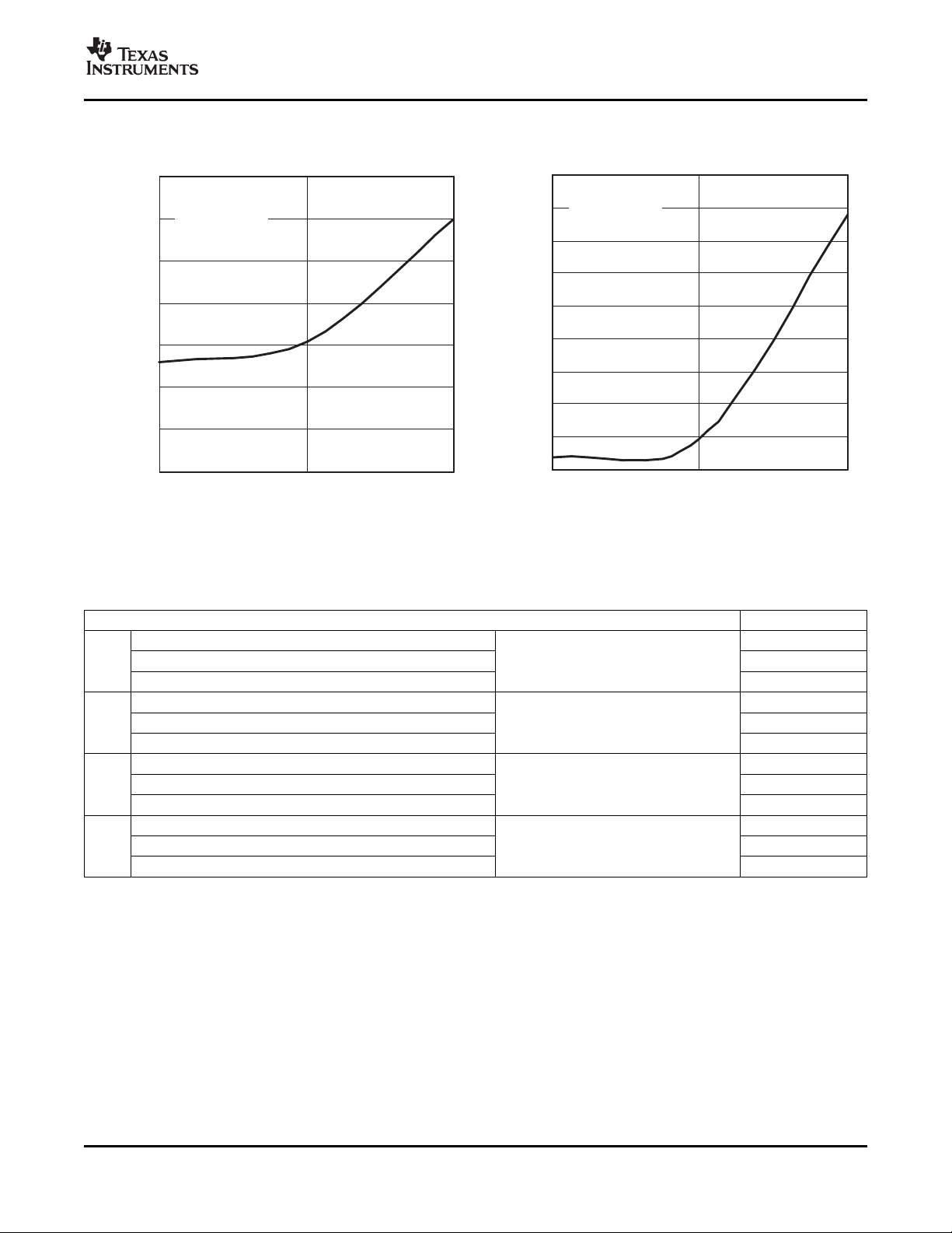
RISE TIME, xVPP FALL TIME, xVPP
vs vs
LOAD CAPACITANCE LOAD CAPACITANCE
TPS2220A , TPS2223A
TPS2224A , TPS2226A
Table of Graphs
Input current, xVCC = 3.3 V 23
I
r
V
I
Input current, xVCC = 5 V vs Junction temperature 24
I
Input current, xVPP = 12 V 25
Static drain-source on-state resistance, 3.3 V to xVCC switch 26
Static drain-source on-state resistance, 5 V to xVCC switch vs Junction temperature 27
DS(on)
Static drain-source on-state resistance, 12 V to xVPP switch 28
xVCC switch voltage drop, 3.3-V input 29
xVCC switch voltage drop, 5-V input vs Load current 30
O
xVPP switch voltage drop, 12-V input 31
Short-circuit current limit, 3.3 V to xVCC 32
Short-circuit current limit, 5 V to xVCC vs Junction temperature 33
OS
Short-circuit current limit, 12 V to xVPP 34
Figure 21. Figure 22.
TYPICAL CHARACTERISTICS
FIGURE
Copyright © 2002 – 2008, Texas Instruments Incorporated Submit Documentation Feedback 15
Product Folder Link(s): TPS2220A TPS2223A TPS2224A TPS2226A
Page 16
www.ti.com
0
20
40
60
80
100
120
140
160
180
−50 −20 10 40 70 100
TJ − Junction Temperature − °C
I
I
− Input Current, xVCC = 3.3 V − Aµ
0
2
4
6
8
10
12
14
−50 −20 10 40 70 100
TJ − Junction Temperature − °C
I
I
− Input Current, xVCC = 5 V − Aµ
0
0.02
0.04
0.06
0.08
0.1
0.12
−50 −20 10 40 70 100
TJ − Junction Temperature − °C
Ω
r
DS(on)
− Static Drain-Source On-State Resistance,
3.3 V to xVCC Switch −
0
20
40
60
80
100
120
−50 −20 10 40 70 100
TJ − Junction Temperature − °C
I
I
− Input Current, xVPP = 12 V − Aµ
TPS2220A , TPS2223A
TPS2224A , TPS2226A
SLVS428E – MAY 2002 – REVISED MSRCH 2008
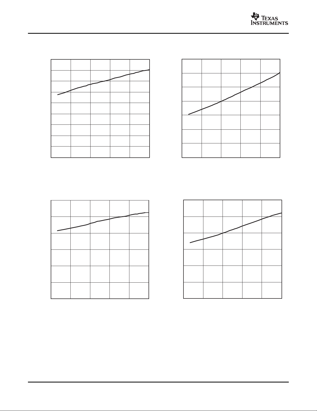
INPUT CURRENT, xVCC = 3.3 V INPUT CURRENT, xVCC = 5 V
JUNCTION TEMPERATURE JUNCTION TEMPERATURE
INPUT CURRENT, xVPP = 12 V 3.3 V TO xVCC SWITCH
JUNCTION TEMPERATURE JUNCTION TEMPERATURE
vs vs
Figure 23. Figure 24.
STATIC DRAIN-SOURCE ON-STATE RESISTANCE,
vs vs
16 Submit Documentation Feedback Copyright © 2002 – 2008, Texas Instruments Incorporated
Figure 25. Figure 26.
Product Folder Link(s): TPS2220A TPS2223A TPS2224A TPS2226A
Page 17
www.ti.com
0
0.02
0.04
0.06
0.08
0.1
0.12
0.14
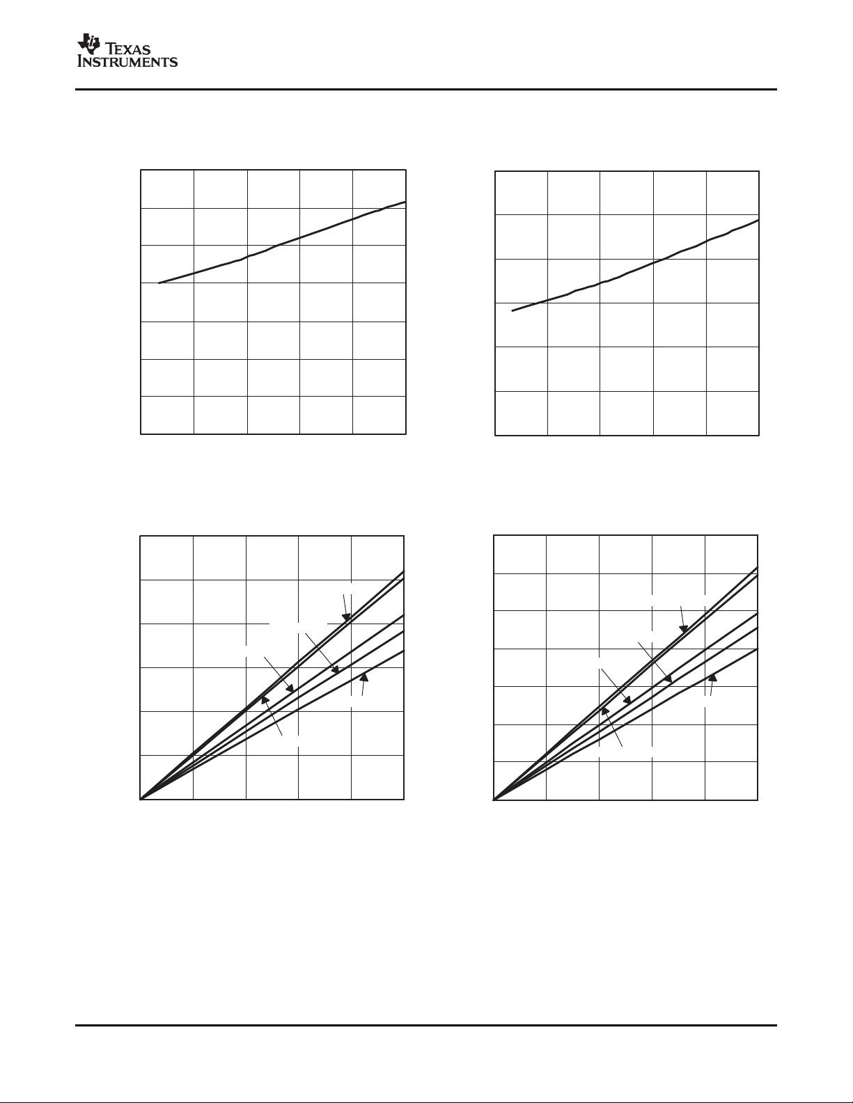
−50 −20 10 40 70 100
TJ − Junction Temperature − °C
Ω
r
DS(on)
− Static Drain-Source On-State Resistance,
5 V to xVCC Switch −
0
0.5
1
1.5
2
2.5
3
−50 −20 10 40 70 100
TJ − Junction Temperature − °C
Ω
r
DS(on)
− Static Drain-Source On-State Resistance,
12 V to xVPP Switch −
0
0.02
0.04
0.06
0.08
0.1
0.12
0 0.2 0.4 0.6 0.8 1
TJ = −40°C
TJ = 85°C
TJ = 100°C
IL − Load Current − A
− xVCC Switch Voltage Drop, 3.3-V Input − VV
O
TJ = 25°C
TJ = 0°C
0
0.02
0.04
0.06
0.08
0.1
0.12
0.14
0 0.2 0.4 0.6 0.8 1
IL − Load Current − A
− xVCC Switch Voltage Drop, 5-V Input − VV
O
TJ = −40°C
TJ = 85°C
TJ = 100°C
TJ = 25°C
TJ = 0°C
TPS2220A , TPS2223A
TPS2224A , TPS2226A
SLVS428E – MAY 2002 – REVISED MSRCH 2008
STATIC DRAIN-SOURCE ON-STATE RESISTANCE, STATIC DRAIN-SOURCE ON-STATE RESISTANCE,
xVCC SWITCH VOLTAGE DROP, 3.3-V INPUT xVCC SWITCH VOLTAGE DROP, 5-V INPUT
5 V TO xVCC SWITCH 12 V TO xVPP SWITCH
vs vs
JUNCTION TEMPERATURE JUNCTION TEMPERATURE
Figure 27. Figure 28.
vs vs
LOAD CURRENT LOAD CURRENT
Copyright © 2002 – 2008, Texas Instruments Incorporated Submit Documentation Feedback 17
Figure 29. Figure 30.
Product Folder Link(s): TPS2220A TPS2223A TPS2224A TPS2226A
Page 18
www.ti.com
0
0.02
0.04
0.06
0.08
0.1
0.12
0.14
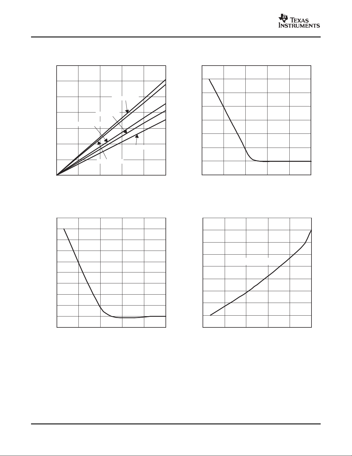
0 0.01 0.02 0.03 0.04 0.05
IL − Load Current − A
− xVPP Switch Voltage Drop, 12-V Input − VV
O
TJ = −40°C
TJ = 85°C
TJ = 100°C
TJ = 25°C
TJ = 0°C
1.355
1.36
1.365
1.37
1.375
1.38
1.385
1.39
1.395
−50 −20 10 40 70 100
TJ − Junction Temperature − °C
I
OS
− Short-Circuit Current Limit, 3.3 V to xVCC − A
1.385
1.39
1.395
1.4
1.405
1.41
1.415
1.42
1.425
1.43
1.435
−50 −20 10 40 70 100
TJ − Junction Temperature − °C
I
OS
− Short-Circuit Current Limit, 5 V to xVCC − A
0.19
0.192
0.194
0.196
0.198
0.2
0.202
0.204
0.206
0.208
−50 −20 10 40 70 100
xVPP = 12 V
TJ − Junction Temperature − °C
I
OS
− Short-Circuit Current Limit, 12 V to xVPP − A
TPS2220A , TPS2223A
TPS2224A , TPS2226A
SLVS428E – MAY 2002 – REVISED MSRCH 2008
xVPP SWITCH VOLTAGE DROP, 12-V INPUT SHORT-CIRCUIT CURRENT LIMIT, 3.3 V TO xVCC
SHORT-CIRCUIT CURRENT LIMIT, 5 V TO xVCC SHORT-CIRCUIT CURRENT LIMIT, 12 V TO xVPP
JUNCTION TEMPERATURE JUNCTION TEMPERATURE
vs vs
LOAD CURRENT JUNCTION TEMPERATURE
Figure 31. Figure 32.
vs vs
18 Submit Documentation Feedback Copyright © 2002 – 2008, Texas Instruments Incorporated
Figure 33. Figure 34.
Product Folder Link(s): TPS2220A TPS2223A TPS2224A TPS2226A
Page 19

www.ti.com
VDS+ V
O(reg)–VPS(reg)–VPCB
IOmax +
V
DS
r
DS(on)
TPS2220A , TPS2223A
TPS2224A , TPS2226A
SLVS428E – MAY 2002 – REVISED MSRCH 2008
APPLICATION INFORMATION
OVERVIEW
PC Cards were initially introduced as a means to add flash memory to portable computers. The idea of add-in
cards quickly took hold, and modems, wireless LANs, global positioning satellite system (GPS), multimedia, and
hard-disk versions were soon available. As the number of PC Card applications grew, the engineering
community quickly recognized the need for a standard to ensure compatibility across platforms. Therefore, the
PCMCIA (Personal Computer Memory Card International Association) was established, comprising members
from leading computer, software, PC Card, and semiconductor manufacturers. One key goal was to realize the
plug-and-play concept, so that cards and hosts from different vendors would be transparently compatible.
PC CARD POWER SPECIFICATION
System compatibility also means power compatibility. The most current set of specifications (PC Card Standard)
set forth by the PCMCIA committee states that power is to be transferred between the host and the card through
eight of the 68 terminals of the PC Card connector. This power interface consists of two V
ground terminals. Multiple V
V
terminals were originally specified as separate signals, but are normally tied together in the host to form a
pp
single node to minimize voltage losses. Card primary power is supplied through the V
programming and erase voltage is supplied through the V
and ground terminals minimize connector-terminal and line resistance. The two
CC
terminals. Cardbus cards of today typically do not
pp
CC
use 12 V, which is now more of an optional requirement in the host.
CC
, two V
, and four
pp
terminals; flash-memory
DESIGNING FOR VOLTAGE REGULATION
The current PCMCIA specification for output voltage regulation, V
typical PC power-system design, the power supply has an output-voltage regulation, V
Also, a voltage drop from the power supply to the PC Card results from resistive losses, V
and the PCMCIA connector. A typical design would limit the total of these resistive losses to less than 1% (50
mV) of the output voltage. Therefore, the allowable voltage drop, V
and TPS2226A would be the PCMCIA voltage regulation less the power supply regulation and less the PCB and
connector resistive drops:
Typically, this would leave 100 mV for the allowable voltage drop across the 5-V switch. The specification for
output voltage regulation of the 3.3-V output is 300 mV; therefore, using the same equation by deducting the
voltage drop percentages (2%) for power-supply regulation and PCB resistive loss (1%), the allowable voltage
drop for the 3.3-V switch is 200 mV. The voltage drop is the output current multiplied by the switch resistance of
the device. Therefore, the maximum output current, IOmax, that can be delivered to the PC Card in regulation is
the allowable voltage drop across the IC, divided by the output-switch resistance.
The xVCC outputs have been designed to deliver the peak and average currents defined by the PC Card
specification within regulation over the operating temperature range. The xVPP outputs of the device have been
designed to deliver 100 mA continuously.
, of the 5-V output is 5% (250 mV). In a
O(reg)
, for the TPS2220A, TPS2223A, TPS2224A,
DS
PS(reg)
PCB
, of 2% (100 mV).
, in the PCB traces
OVERCURRENT AND OVERTEMPERATURE PROTECTION
PC Cards are inherently subject to damage that can result from mishandling. Host systems require protection
against short-circuited cards that can lead to power-supply or PCB trace damage. Even extremely robust
systems can undergo rapid battery discharge into a damaged PC Card, resulting in the sudden and unacceptable
loss of system power. In comparison, the reliability of fused systems is poor because blown fuses require
troubleshooting and repair, usually by the manufacturer.
The TPS2220A, TPS2223A, TPS2224A, and TPS2226A take a two-pronged approach to overcurrent protection,
which is designed to activate if an output is shorted or when an overcurrent condition is present when switches
are powered up. First, instead of fuses, sense FETs monitor each of the xVCC and xVPP power outputs. Unlike
Copyright © 2002 – 2008, Texas Instruments Incorporated Submit Documentation Feedback 19
Product Folder Link(s): TPS2220A TPS2223A TPS2224A TPS2226A
Page 20

www.ti.com
TPS2220A , TPS2223A
TPS2224A , TPS2226A
SLVS428E – MAY 2002 – REVISED MSRCH 2008
sense resistors or polyfuses, these FETs do not add to the series resistance of the switch; therefore, voltage and
power losses are reduced. Overcurrent sensing is applied to each output separately. Excessive current
generates an error signal that limits the output current of only the affected output, preventing damage to the host.
Each xVCC output overcurrent limits from 1 A to 2.0 A, typically around 1.6 A; the xVPP outputs limit from 100
mA to 250 mA, typically around 200 mA.
Second, when an overcurrent condition is detected, the TPS2220A, TPS2223A, TPS2224A, and TPS2226A
assert an active low OC signal that can be monitored by the microprocessor or controller to initiate diagnostics
and/or send the user a warning message. If an overcurrent condition persists, causing the IC to exceed its
maximum junction temperature, thermal-protection circuitry activates, shutting down all power outputs until the
device cools to within a safe operating region, which is ensured by a thermal shutdown hysteresis. Thermal
limiting prevents destruction of the IC from overheating beyond the package power-dissipation ratings.
During power up, the devices control the rise times of the xVCC and xVPP outputs and limit the inrush current
into a large load capacitance, faulty card, or connector.
12-V SUPPLY NOT REQUIRED
Some PC Card switches use the externally supplied 12 V to power gate drive and other chip functions, which
requires that power be present at all times. The TPS2220A, TPS2224A and TPS2226A offer considerable power
savings by using an internal charge pump to generate the required higher gate drive voltages from the 3.3-V
input. Therefore, the external 12-V supply can be disabled except when needed by the PC Card in the slot,
thereby extending battery lifetime. A special feature in the 12-V circuitry actually helps to reduce the supply
current demanded from the 3.3-V input. When 12 V is supplied and requested at the VPP output, a voltage
selection circuit draws the charge-pump drive current for the 12-V FETs from the 12-V input. This selection is
automatic and effectively reduces demand fluctuations on the normal 3.3-V VCC rail. For proper operation of this
feature, a minimum 3.3-V input capacitance of 4.7 µ F is recommended, and a minimum 12-V input ramp-up rate
of 12 V/50 ms (240 V/s) is required. Additional power savings are realized during a software shutdown in which
quiescent current drops to a maximum of 1 µ A.
VOLTAGE-TRANSITIONING REQUIREMENT
PC Cards, like portables, are migrating from 5 V to 3.3 V to minimize power consumption, optimize board space,
and increase logic speeds. The TPS2220A, TPS2223A, TPS2224A, and TPS2226A meet all combinations of
power delivery as currently defined in the PCMCIA standard. The latest protocol accommodates mixed 3.3-V/5-V
systems by first powering the card with 5 V, then polling it to determine its 3.3-V compatibility. The PCMCIA
specification requires that the capacitors on 3.3-V-compatible cards be discharged to below 0.8 V before
applying 3.3-V power. This action ensures that sensitive 3.3-V circuitry is not subjected to any residual 5-V
charge and functions as a power reset. PC Card specification requires that V
be discharged within 100 ms. PC
CC
Card resistance cannot be relied on to provide a discharge path for voltages stored on PC Card capacitance
because of possible high-impedance isolation by power-management schemes. The devices include discharge
transistors on all xVCC and xVPP outputs to meet the specification requirement.
SHUTDOWN MODE
In the shutdown mode, which can be controlled by SHDN or bit D8 of the input serial DATA word, each of the
xVCC and xVPP outputs is forced to a high-impedance state. In this mode, the chip quiescent current is reduced
to 1 µ A or less to conserve battery power.
POWER-SUPPLY CONSIDERATIONS
These switches have multiple pins for each 3.3-V (except for TPS2220A) and 5-V power input and for the
switched xVCC outputs. Any individual pin can conduct the rated input or output current. Unless all pins are
connected in parallel, the series resistance is higher than that specified, resulting in increased voltage drops and
power loss. It is recommended that all input and output power pins be paralleled for optimum operation.
To increase the noise immunity of the TPS2220A, TPS2223A, TPS2224A, and TPS2226A, the power-supply
inputs should be bypassed with at least a 4.7- µ F electrolytic or tantalum capacitor paralleled by a 0.047- µ F to
20 Submit Documentation Feedback Copyright © 2002 – 2008, Texas Instruments Incorporated
Product Folder Link(s): TPS2220A TPS2223A TPS2224A TPS2226A
Page 21

www.ti.com
PD+ r
DS(on)
I
2
T
J
+
ǒȍ
PD R
qJA
Ǔ
) T
A
where:
R
θJA
is the inverse of the derating factor given in the dissipation rating table.
TPS2220A , TPS2223A
TPS2224A , TPS2226A
SLVS428E – MAY 2002 – REVISED MSRCH 2008
0.1- µ F ceramic capacitor. It is strongly recommended that the switched outputs be bypassed with a 0.1- µ F (or
larger) ceramic capacitor; doing so improves the immunity of the IC to electrostatic discharge (ESD). Care should
be taken to minimize the inductance of PCB traces between the devices and the load. High switching currents
can produce large negative voltage transients, which forward biases substrate diodes, resulting in unpredictable
performance. Similarly, no pin should be taken below -0.3 V.
RESET INPUT
To ensure that cards are in a known state after power brownouts or system initialization, the PC Cards should be
reset at the same time as the host by applying low-impedance paths from xVCC and xVPP terminals to ground.
A low-impedance output state allows discharging of residual voltage remaining on PC Card filter capacitance,
permitting the system (host and PC Cards) to be powered up concurrently. The active low RESET input closes
internal ground switches S1, S4, S7, and S11 with all other switches left open. The TPS2220A, TPS2223A,
TPS2224A, and TPS2226A remain in the low-impedance output state until the signal is de-asserted and further
data is clocked in and latched. The input serial data cannot be latched during reset mode. RESET is provided for
direct compatibility with systems that use an active-low reset voltage supervisor. The RESET pin has an internal
150-k Ω pullup resistor.
CALCULATING JUNCTION TEMPERATURE
The switch resistance, r
is dependent on both r
through Figure 28 , using an initial temperature estimate about 30 ° C above ambient. Then, calculate the power
dissipation for each switch, using the formula:
, is dependent on the junction temperature, TJ, of the die. The junction temperature
DS(on)
and the current through the switch. To calculate TJ, first find r
DS(on)
DS(on)
from Figure 26
Next, sum the power dissipation of all switches and calculate the junction temperature:
Compare the calculated junction temperature with the initial temperature estimate. If the temperatures are not
within a few degrees of each other, recalculate using the calculated temperature as the initial estimate.
LOGIC INPUTS AND OUTPUTS
The serial interface consists of the DATA, CLOCK, and LATCH leads. The data is clocked in on the positive
edge of the clock (see Figure 2 ). The 11-bit (D0-D10) serial data word is loaded during the positive edge of the
latch signal. The positive edge of the latch signal should occur before the next positive edge of the clock occurs.
The serial interface of the device is compatible with serial-interface PCMCIA controllers.
An overcurrent output ( OC) is provided to indicate an overcurrent or overtemperature condition in any of the
xVCC and xVPP outputs as previously discussed.
Copyright © 2002 – 2008, Texas Instruments Incorporated Submit Documentation Feedback 21
Product Folder Link(s): TPS2220A TPS2223A TPS2224A TPS2226A
Page 22
PACKAGE OPTION ADDENDUM
www.ti.com
PACKAGING INFORMATION
Orderable Device Status
TPS2220ADBR ACTIVE SSOP DB 24 2000 Green (RoHS
TPS2220ADBRG4 ACTIVE SSOP DB 24 2000 Green (RoHS
TPS2220APWP ACTIVE HTSSOP PWP 24 60 Green (RoHS
TPS2220APWPG4 ACTIVE HTSSOP PWP 24 60 Green (RoHS
TPS2220APWPR ACTIVE HTSSOP PWP 24 2000 Green (RoHS
TPS2220APWPRG4 ACTIVE HTSSOP PWP 24 2000 Green (RoHS
TPS2223ADB ACTIVE SSOP DB 24 60 Green (RoHS
TPS2223ADBG4 ACTIVE SSOP DB 24 60 Green (RoHS
TPS2223ADBR ACTIVE SSOP DB 24 2000 Green (RoHS
TPS2223ADBRG4 ACTIVE SSOP DB 24 2000 Green (RoHS
TPS2223APWP ACTIVE HTSSOP PWP 24 60 Green (RoHS
TPS2223APWPG4 ACTIVE HTSSOP PWP 24 60 Green (RoHS
TPS2223APWPR ACTIVE HTSSOP PWP 24 2000 Green (RoHS
TPS2223APWPRG4 ACTIVE HTSSOP PWP 24 2000 Green (RoHS
TPS2224ADB ACTIVE SSOP DB 24 60 Green (RoHS
TPS2224ADBG4 ACTIVE SSOP DB 24 60 Green (RoHS
TPS2224ADBR ACTIVE SSOP DB 24 2000 Green (RoHS
Package Type Package
(1)
Drawing
Pins Package
Qty
Eco Plan
(2)
& no Sb/Br)
& no Sb/Br)
& no Sb/Br)
& no Sb/Br)
& no Sb/Br)
& no Sb/Br)
& no Sb/Br)
& no Sb/Br)
& no Sb/Br)
& no Sb/Br)
& no Sb/Br)
& no Sb/Br)
& no Sb/Br)
& no Sb/Br)
& no Sb/Br)
& no Sb/Br)
& no Sb/Br)
Lead/Ball Finish MSL Peak Temp
(3)
CU NIPDAU Level-1-260C-UNLIM -40 to 85 TPS2220A
CU NIPDAU Level-1-260C-UNLIM -40 to 85 TPS2220A
CU NIPDAU Level-2-260C-1 YEAR -40 to 85 TPS2220A
CU NIPDAU Level-2-260C-1 YEAR -40 to 85 TPS2220A
CU NIPDAU Level-2-260C-1 YEAR -40 to 85 TPS2220A
CU NIPDAU Level-2-260C-1 YEAR -40 to 85 TPS2220A
CU NIPDAU Level-1-260C-UNLIM -40 to 85 TPS2223A
CU NIPDAU Level-1-260C-UNLIM -40 to 85 TPS2223A
CU NIPDAU Level-1-260C-UNLIM -40 to 85 TPS2223A
CU NIPDAU Level-1-260C-UNLIM -40 to 85 TPS2223A
CU NIPDAU Level-2-260C-1 YEAR -40 to 85 TPS2223A
CU NIPDAU Level-2-260C-1 YEAR -40 to 85 TPS2223A
CU NIPDAU Level-2-260C-1 YEAR -40 to 85 TPS2223A
CU NIPDAU Level-2-260C-1 YEAR -40 to 85 TPS2223A
CU NIPDAU Level-1-260C-UNLIM -40 to 85 TPS2224A
CU NIPDAU Level-1-260C-UNLIM -40 to 85 TPS2224A
CU NIPDAU Level-1-260C-UNLIM -40 to 85 TPS2224A
Op Temp (°C) Top-Side Markings
11-Apr-2013
Samples
(4)
Addendum-Page 1
Page 23
PACKAGE OPTION ADDENDUM
www.ti.com
Orderable Device Status
TPS2224ADBRG4 ACTIVE SSOP DB 24 2000 Green (RoHS
TPS2224APWP ACTIVE HTSSOP PWP 24 60 Green (RoHS
TPS2224APWPG4 ACTIVE HTSSOP PWP 24 60 Green (RoHS
TPS2224APWPR ACTIVE HTSSOP PWP 24 2000 Green (RoHS
TPS2224APWPRG4 ACTIVE HTSSOP PWP 24 2000 Green (RoHS
TPS2226ADB ACTIVE SSOP DB 30 50 Green (RoHS
TPS2226ADBG4 ACTIVE SSOP DB 30 50 Green (RoHS
TPS2226ADBR ACTIVE SSOP DB 30 2000 Green (RoHS
TPS2226ADBRG4 ACTIVE SSOP DB 30 2000 Green (RoHS
(1)
The marketing status values are defined as follows:
ACTIVE: Product device recommended for new designs.
LIFEBUY: TI has announced that the device will be discontinued, and a lifetime-buy period is in effect.
NRND: Not recommended for new designs. Device is in production to support existing customers, but TI does not recommend using this part in a new design.
PREVIEW: Device has been announced but is not in production. Samples may or may not be available.
OBSOLETE: TI has discontinued the production of the device.
Package Type Package
(1)
Drawing
Pins Package
Qty
Eco Plan
(2)
& no Sb/Br)
& no Sb/Br)
& no Sb/Br)
& no Sb/Br)
& no Sb/Br)
& no Sb/Br)
& no Sb/Br)
& no Sb/Br)
& no Sb/Br)
Lead/Ball Finish MSL Peak Temp
(3)
CU NIPDAU Level-1-260C-UNLIM -40 to 85 TPS2224A
CU NIPDAU Level-2-260C-1 YEAR -40 to 85 TPS2224A
CU NIPDAU Level-2-260C-1 YEAR -40 to 85 TPS2224A
CU NIPDAU Level-2-260C-1 YEAR -40 to 85 TPS2224A
CU NIPDAU Level-2-260C-1 YEAR -40 to 85 TPS2224A
CU NIPDAU Level-1-260C-UNLIM -40 to 85 TPS2226A
CU NIPDAU Level-1-260C-UNLIM -40 to 85 TPS2226A
CU NIPDAU Level-1-260C-UNLIM -40 to 85 TPS2226A
CU NIPDAU Level-1-260C-UNLIM -40 to 85 TPS2226A
Op Temp (°C) Top-Side Markings
(4)
11-Apr-2013
(2)
Eco Plan - The planned eco-friendly classification: Pb-Free (RoHS), Pb-Free (RoHS Exempt), or Green (RoHS & no Sb/Br) - please check http://www.ti.com/productcontent for the latest availability
information and additional product content details.
TBD: The Pb-Free/Green conversion plan has not been defined.
Pb-Free (RoHS): TI's terms "Lead-Free" or "Pb-Free" mean semiconductor products that are compatible with the current RoHS requirements for all 6 substances, including the requirement that
lead not exceed 0.1% by weight in homogeneous materials. Where designed to be soldered at high temperatures, TI Pb-Free products are suitable for use in specified lead-free processes.
Pb-Free (RoHS Exempt): This component has a RoHS exemption for either 1) lead-based flip-chip solder bumps used between the die and package, or 2) lead-based die adhesive used between
the die and leadframe. The component is otherwise considered Pb-Free (RoHS compatible) as defined above.
Green (RoHS & no Sb/Br): TI defines "Green" to mean Pb-Free (RoHS compatible), and free of Bromine (Br) and Antimony (Sb) based flame retardants (Br or Sb do not exceed 0.1% by weight
in homogeneous material)
(3)
MSL, Peak Temp. -- The Moisture Sensitivity Level rating according to the JEDEC industry standard classifications, and peak solder temperature.
Samples
Addendum-Page 2
Page 24

PACKAGE OPTION ADDENDUM
www.ti.com
(4)
Multiple Top-Side Markings will be inside parentheses. Only one Top-Side Marking contained in parentheses and separated by a "~" will appear on a device. If a line is indented then it is a
continuation of the previous line and the two combined represent the entire Top-Side Marking for that device.
11-Apr-2013
Important Information and Disclaimer:The information provided on this page represents TI's knowledge and belief as of the date that it is provided. TI bases its knowledge and belief on information
provided by third parties, and makes no representation or warranty as to the accuracy of such information. Efforts are underway to better integrate information from third parties. TI has taken and
continues to take reasonable steps to provide representative and accurate information but may not have conducted destructive testing or chemical analysis on incoming materials and chemicals.
TI and TI suppliers consider certain information to be proprietary, and thus CAS numbers and other limited information may not be available for release.
In no event shall TI's liability arising out of such information exceed the total purchase price of the TI part(s) at issue in this document sold by TI to Customer on an annual basis.
Addendum-Page 3
Page 25
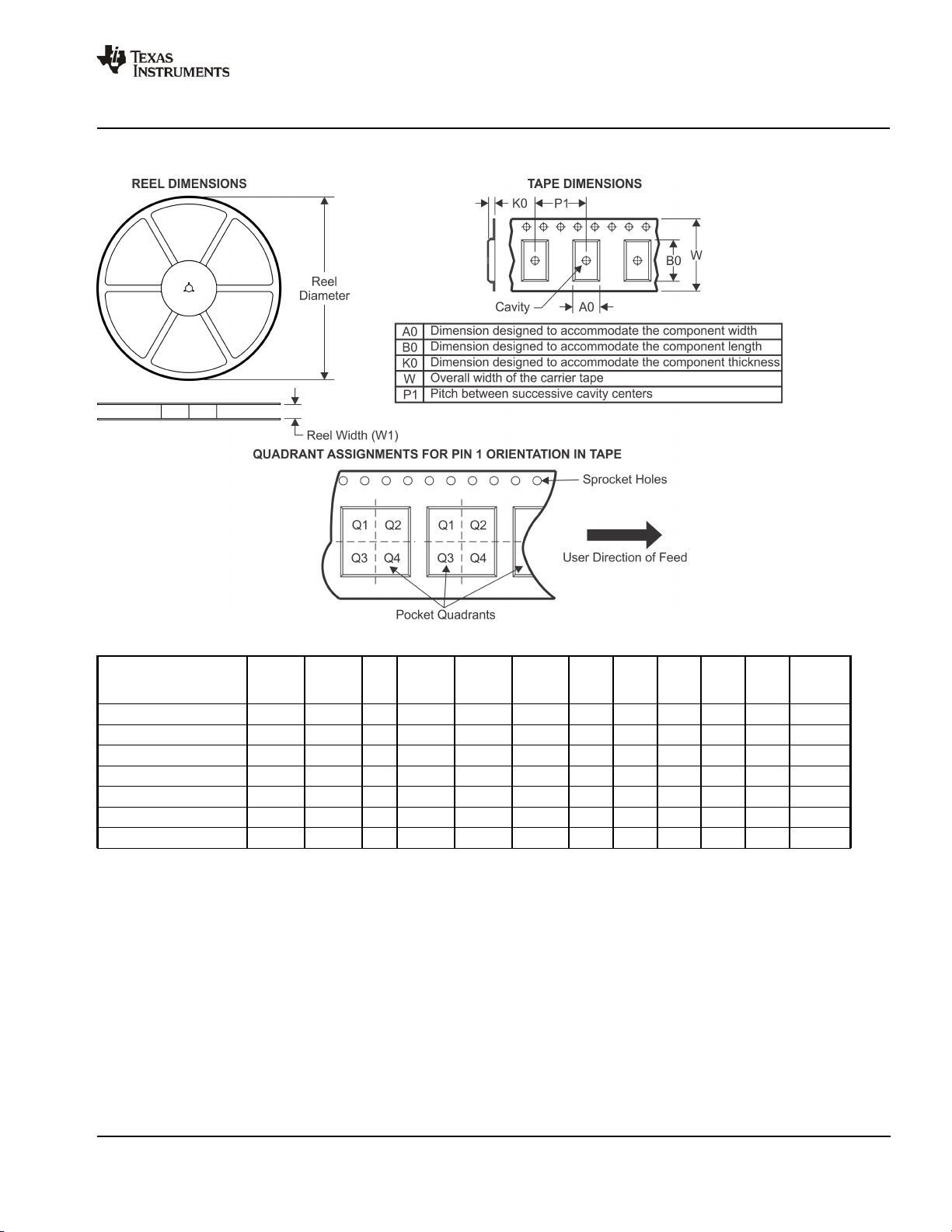
PACKAGE MATERIALS INFORMATION
www.ti.com 24-Apr-2013
TAPE AND REEL INFORMATION
*All dimensions are nominal
Device Package
Type
TPS2220ADBR SSOP DB 24 2000 330.0 16.4 8.2 8.8 2.5 12.0 16.0 Q1
TPS2220APWPR HTSSOP PWP 24 2000 330.0 16.4 6.95 8.3 1.6 8.0 16.0 Q1
TPS2223ADBR SSOP DB 24 2000 330.0 16.4 8.2 8.8 2.5 12.0 16.0 Q1
TPS2223APWPR HTSSOP PWP 24 2000 330.0 16.4 6.95 8.3 1.6 8.0 16.0 Q1
TPS2224ADBR SSOP DB 24 2000 330.0 16.4 8.2 8.8 2.5 12.0 16.0 Q1
TPS2224APWPR HTSSOP PWP 24 2000 330.0 16.4 6.95 8.3 1.6 8.0 16.0 Q1
TPS2226ADBR SSOP DB 30 2000 330.0 16.4 8.2 10.5 2.5 12.0 16.0 Q1
Package
Drawing
Pins SPQ Reel
Diameter
(mm)
Reel
Width
W1 (mm)
A0
(mm)B0(mm)K0(mm)P1(mm)W(mm)
Pin1
Quadrant
Pack Materials-Page 1
Page 26
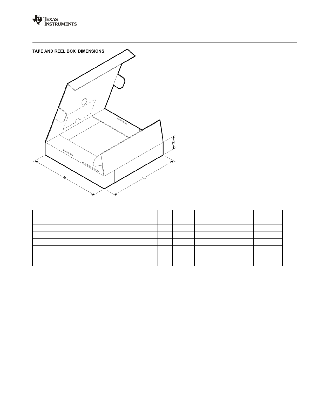
PACKAGE MATERIALS INFORMATION
www.ti.com 24-Apr-2013
*All dimensions are nominal
Device Package Type Package Drawing Pins SPQ Length (mm) Width (mm) Height (mm)
TPS2220ADBR SSOP DB 24 2000 367.0 367.0 38.0
TPS2220APWPR HTSSOP PWP 24 2000 367.0 367.0 38.0
TPS2223ADBR SSOP DB 24 2000 367.0 367.0 38.0
TPS2223APWPR HTSSOP PWP 24 2000 367.0 367.0 35.0
TPS2224ADBR SSOP DB 24 2000 367.0 367.0 38.0
TPS2224APWPR HTSSOP PWP 24 2000 367.0 367.0 38.0
TPS2226ADBR SSOP DB 30 2000 367.0 367.0 38.0
Pack Materials-Page 2
Page 27
Page 28
Page 29
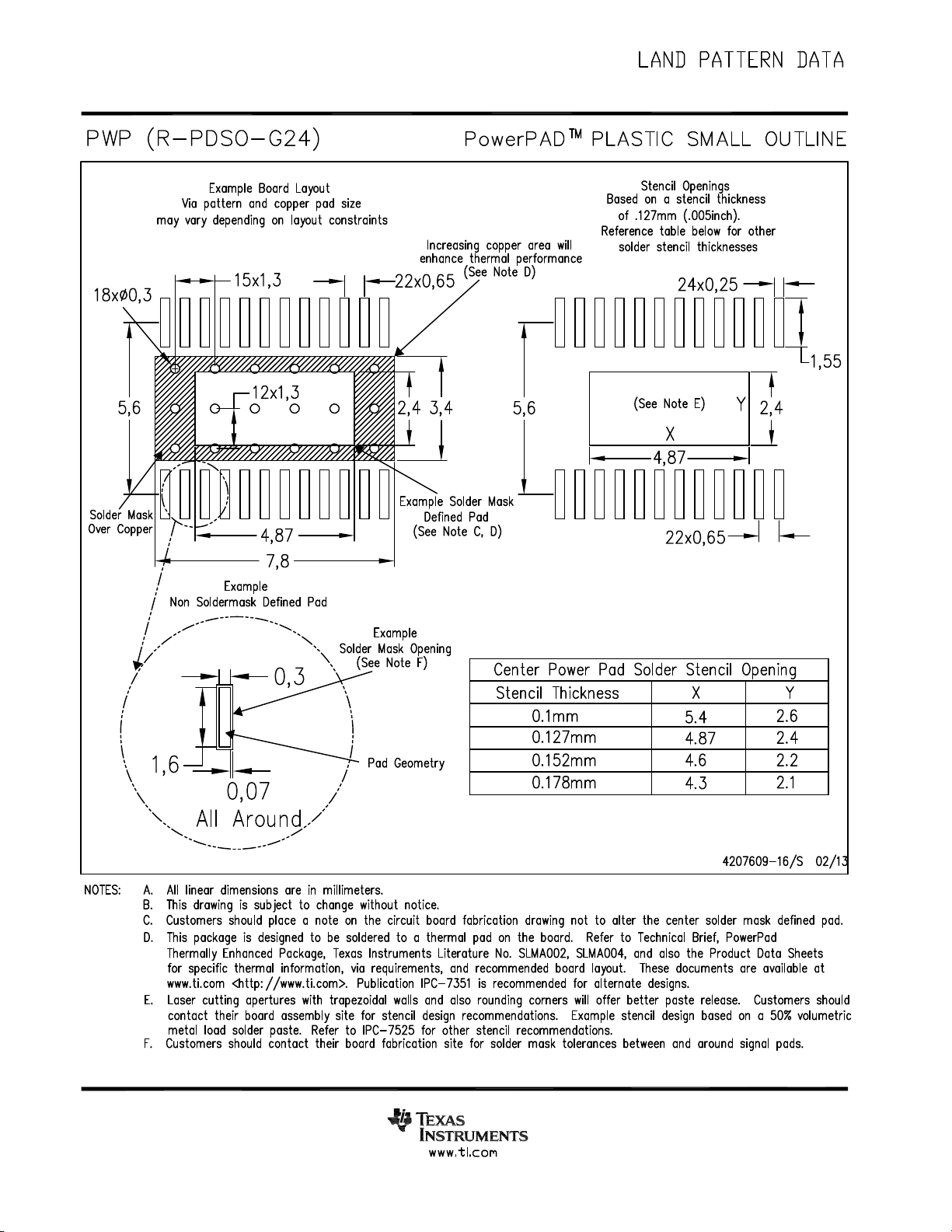
Page 30
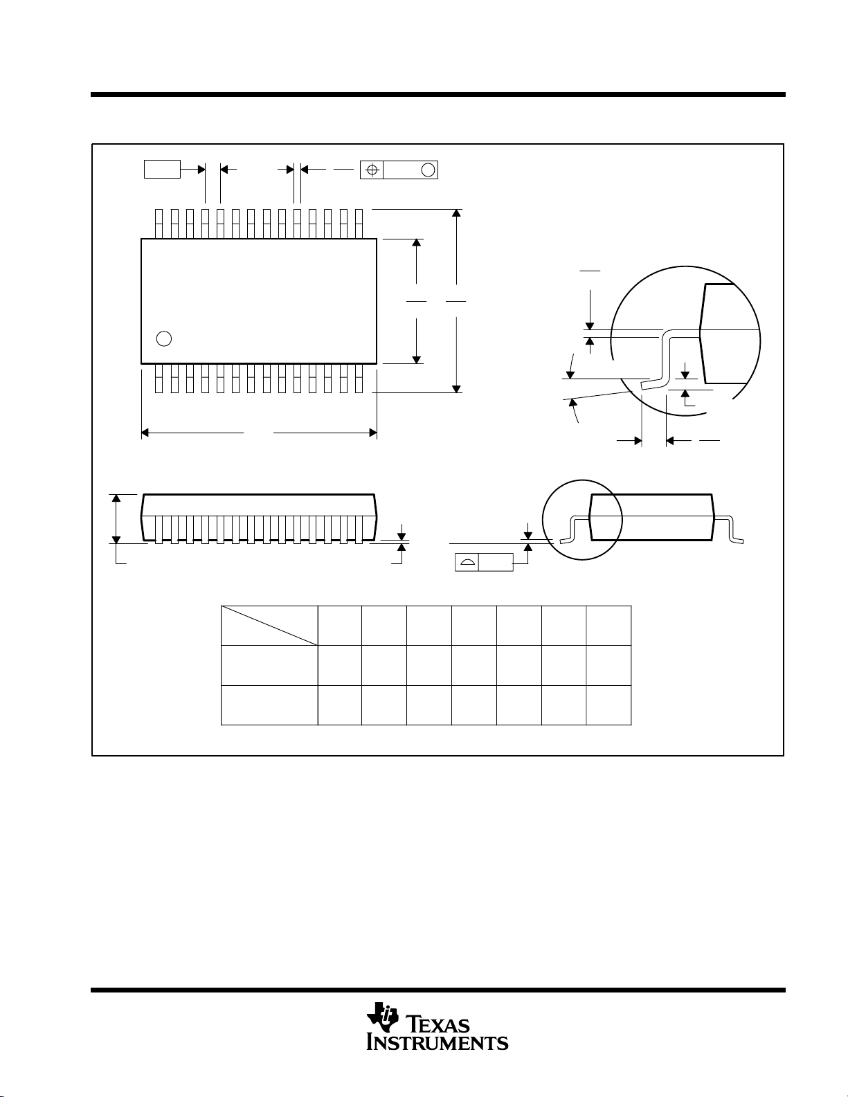
MECHANICAL DATA
MSSO002E – JANUARY 1995 – REVISED DECEMBER 2001
DB (R-PDSO-G**) PLASTIC SMALL-OUTLINE
28 PINS SHOWN
0,65
28
1
2,00 MAX
0,38
0,22
15
14
A
0,05 MIN
0,15
5,60
5,00
M
8,20
7,40
Seating Plane
0,10
0,25
0,09
0°–ā8°
Gage Plane
0,25
0,95
0,55
PINS **
DIM
A MAX
A MIN
NOTES: A. All linear dimensions are in millimeters.
B. This drawing is subject to change without notice.
C. Body dimensions do not include mold flash or protrusion not to exceed 0,15.
D. Falls within JEDEC MO-150
14
6,50
6,50
5,905,90
2016
7,50
6,90
24
8,50
28
10,50
9,907,90
30
10,50
9,90
38
12,90
12,30
4040065 /E 12/01
POST OFFICE BOX 655303 • DALLAS, TEXAS 75265
Page 31

IMPORTANT NOTICE
Texas Instruments Incorporated and its subsidiaries (TI) reserve the right to make corrections, enhancements, improvements and other
changes to its semiconductor products and services per JESD46, latest issue, and to discontinue any product or service per JESD48, latest
issue. Buyers should obtain the latest relevant information before placing orders and should verify that such information is current and
complete. All semiconductor products (also referred to herein as “components”) are sold subject to TI’s terms and conditions of sale
supplied at the time of order acknowledgment.
TI warrants performance of its components to the specifications applicable at the time of sale, in accordance with the warranty in TI’s terms
and conditions of sale of semiconductor products. Testing and other quality control techniques are used to the extent TI deems necessary
to support this warranty. Except where mandated by applicable law, testing of all parameters of each component is not necessarily
performed.
TI assumes no liability for applications assistance or the design of Buyers’ products. Buyers are responsible for their products and
applications using TI components. To minimize the risks associated with Buyers’ products and applications, Buyers should provide
adequate design and operating safeguards.
TI does not warrant or represent that any license, either express or implied, is granted under any patent right, copyright, mask work right, or
other intellectual property right relating to any combination, machine, or process in which TI components or services are used. Information
published by TI regarding third-party products or services does not constitute a license to use such products or services or a warranty or
endorsement thereof. Use of such information may require a license from a third party under the patents or other intellectual property of the
third party, or a license from TI under the patents or other intellectual property of TI.
Reproduction of significant portions of TI information in TI data books or data sheets is permissible only if reproduction is without alteration
and is accompanied by all associated warranties, conditions, limitations, and notices. TI is not responsible or liable for such altered
documentation. Information of third parties may be subject to additional restrictions.
Resale of TI components or services with statements different from or beyond the parameters stated by TI for that component or service
voids all express and any implied warranties for the associated TI component or service and is an unfair and deceptive business practice.
TI is not responsible or liable for any such statements.
Buyer acknowledges and agrees that it is solely responsible for compliance with all legal, regulatory and safety-related requirements
concerning its products, and any use of TI components in its applications, notwithstanding any applications-related information or support
that may be provided by TI. Buyer represents and agrees that it has all the necessary expertise to create and implement safeguards which
anticipate dangerous consequences of failures, monitor failures and their consequences, lessen the likelihood of failures that might cause
harm and take appropriate remedial actions. Buyer will fully indemnify TI and its representatives against any damages arising out of the use
of any TI components in safety-critical applications.
In some cases, TI components may be promoted specifically to facilitate safety-related applications. With such components, TI’s goal is to
help enable customers to design and create their own end-product solutions that meet applicable functional safety standards and
requirements. Nonetheless, such components are subject to these terms.
No TI components are authorized for use in FDA Class III (or similar life-critical medical equipment) unless authorized officers of the parties
have executed a special agreement specifically governing such use.
Only those TI components which TI has specifically designated as military grade or “enhanced plastic” are designed and intended for use in
military/aerospace applications or environments. Buyer acknowledges and agrees that any military or aerospace use of TI components
which have not been so designated is solely at the Buyer's risk, and that Buyer is solely responsible for compliance with all legal and
regulatory requirements in connection with such use.
TI has specifically designated certain components as meeting ISO/TS16949 requirements, mainly for automotive use. In any case of use of
non-designated products, TI will not be responsible for any failure to meet ISO/TS16949.
Products Applications
Audio www.ti.com/audio Automotive and Transportation www.ti.com/automotive
Amplifiers amplifier.ti.com Communications and Telecom www.ti.com/communications
Data Converters dataconverter.ti.com Computers and Peripherals www.ti.com/computers
DLP® Products www.dlp.com Consumer Electronics www.ti.com/consumer-apps
DSP dsp.ti.com Energy and Lighting www.ti.com/energy
Clocks and Timers www.ti.com/clocks Industrial www.ti.com/industrial
Interface interface.ti.com Medical www.ti.com/medical
Logic logic.ti.com Security www.ti.com/security
Power Mgmt power.ti.com Space, Avionics and Defense www.ti.com/space-avionics-defense
Microcontrollers microcontroller.ti.com Video and Imaging www.ti.com/video
RFID www.ti-rfid.com
OMAP Applications Processors www.ti.com/omap TI E2E Community e2e.ti.com
Wireless Connectivity www.ti.com/wirelessconnectivity
Mailing Address: Texas Instruments, Post Office Box 655303, Dallas, Texas 75265
Copyright © 2013, Texas Instruments Incorporated
 Loading...