

Page 1

PROTECTION PRODUCTS
1
www.semtech.com
PROTECTION PRODUCTS
SLVDA2.8
Low Voltage TVS Diode Array
For ESD & Latch-Up Protection
Description
Features
Circuit Diagram (Each Line) Schematic & PIN Configuration
Revision 9/2000
The SLV series of transient voltage suppressors are
designed to protect low voltage semiconductor components which are connected to data and transmission
lines from transients caused by electrostatic discharge
(ESD), lightning and other induced voltage surges.
The devices are constructed using Semtechs proprietary EPD process technology. The EPD process provides low standoff voltages with significant reductions
in leakage currents and capacitance over silicon
avalanche diode processes. The SLV series is specifically designed for protecting low voltage components
such as microprocessors, ASICs, I/O transceivers, and
high speed RAM. They provide ESD and latch-up
protection for power and I/O ports, microprocessor bus
interfaces, high speed data and video transmission
lines, and low power portable and wireless systems.
The SLV series TVS diodes will meet the surge requirements of IEC 61000-4-2, Level 4, Human Body
Model for air and contact discharge.
The low clamping voltage of the SLV minimizes the
stress on the protected transceiver. The SO-8 package
allows flexibility in the design of crowded circuit
boards.
Applications
Mechanical Characteristics
u ESD and Latch-Up Protection
u Analog Inputs
u WAN/LAN Equipment
u Low Voltage ASICs
u Instrumentation
u Low Power Systems
u 300 watts peak pulse power (tp = 8/20µs)
u Transient protection for data lines to
IEC 61000-4-2 (ESD) 15kV (air), 8kV (contact)
IEC 61000-4-4 (EFT) 40A (5/50ns)
IEC 61000-4-5 (Lightning) 12A (1.2/50µs)
u Protects up to four bidirectional lines
u Working Voltages: 2.8V & 3.3V
u Low leakage current for low power applications
u Low operating voltage ideal for latch-up protection
u Low capacitance
u Low clamping voltage
u Solid-state EPD TVS technology
u JEDEC SO-8 package
u Molding compound flammability rating: UL 94V-0
u Marking : Part number, date code, logo
u Packaging : Tape and Reel per EIA 481
S0-8 (Top View)
1
2
3
4
5
6
7
8
Page 2

2ã 2000 Semtech Corp.
www.semtech.com
PROTECTION PRODUCTS
PROTECTION PRODUCTS
SLVDA2.8
Absolute Maximum Rating
Electrical Characteristics
8.2ADVLS
retemaraPlobmySsnoitidnoCmuminiMlacipyTmumixaMstinU
egatloVffO-dnatSesreveRV
MWR
8.2V
egatloVhguorhT-hcnuPV
TP
I
TP
Aµ2=0.3V
egatloVkcaB-panSV
BS
I
BS
Am05=8.2V
tnerruCegakaeLesreveRI
R
V
MWR
C°52=T,V8.2=1Aµ
egatloVgnipmalCV
C
I
PP
sµ02/8=pt,A1=1.4V
egatloVgnipmalCV
C
I
PP
sµ02/8=pt,A5=3.5V
tnerruCesluPkaePmumixaMI
PP
sµ02/8=pt42A
ecnaticapaCnoitcnuJC
j
dnasniPO/IneewteB
dnG
V
R
zHM1=f,V0=
001Fp
gnitaRlobmySeulaVstinU
)sµ02/8=pt(rewoPesluPkaePP
kp
003sttaW
)sµ02/8=pt(tnerruCesluPkaePI
PP
42A
erutarepmeTgniredloSdaeLT
L
).ces01(062C°
erutarepmeTgnitarepOT
J
521+ot55-C°
erutarepmeTegarotST
GTS
051+ot55-C°
Page 3

3
ã 2000 Semtech Corp.
www.semtech.com
PROTECTION PRODUCTS
SLVDA2.8
Typical Characteristics
Non-Repetitive Peak Pulse Power vs. Pulse Time
0
10
20
30
40
50
60
70
80
90
100
110
0 25 50 75 100 125 150
Ambient Temperature - T
A
(oC)
% of Rated Power or I
PP
Power Derating Curve
Pulse Waveform
0
10
20
30
40
50
60
70
80
90
100
110
0 5 10 15 20 25 30
Time (µs)
Percent of I
PP
e
-t
td = IPP/2
Waveform
Parameters:
tr = 8µs
td = 20µs
0.01
0.1
1
10
0.1 1 10 100 1000
Pulse Duration - tp (µs)
Peak Pulse Power - P
PP
(kW)
ESD Pulse Waveform (IEC 61000-4-2)
IEC 61000-4-2 Discharge Parameters
leveLtsriF
kaeP
tnerruC
)A(
kaeP
tnerruC
sn03ta
)A(
kaeP
tnerruC
sn06ta
)A(
tseT
egatloV
tcatnoC(
)egrahcsiD
)Vk(
tseT
egatloV
riA(
)egrahcsiD
)Vk(
15.748 2 2
25184 4 4
35.222166 8
403618 8 51
Page 4
4ã 2000 Semtech Corp.
www.semtech.com
PROTECTION PRODUCTS
PROTECTION PRODUCTS
SLVDA2.8
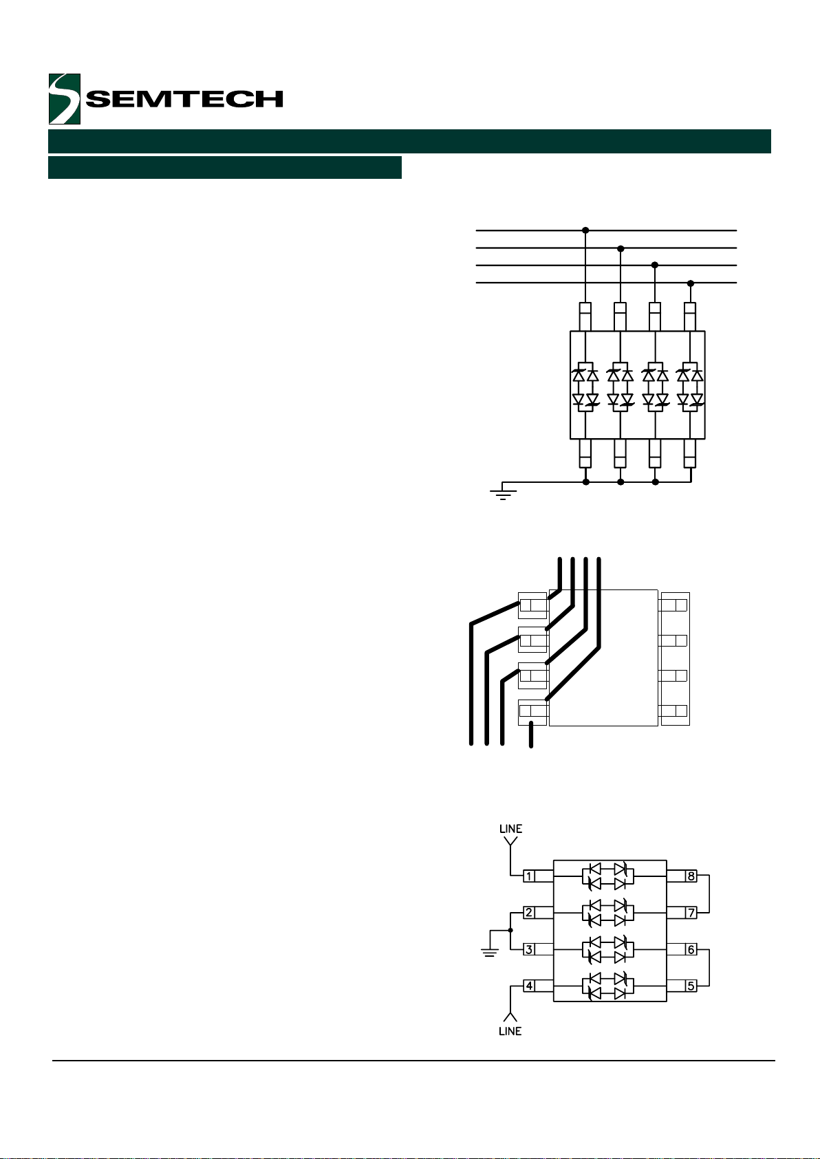
I/O Line Protection
Typical Connection
Device Connection for Protection of Four Data Lines
The SLVDA series devices are designed to protect up to
four data lines. The devices are connected as follows:
l Common mode protection of four data lines is
achieved by connecting data lines at pins 1 - 4.
Pins 5 - 8 are connected to ground (Device is
symmetrical so connections may be reversed to
serve a specific application). The ground connections should be made directly to the ground plane
for best results. The path length is kept as short
as possible to reduce the effects of parasitic
inductance in the board traces.
l Protecting 5V lines: The designer may take advan-
tage of the superior reverse leakage and capacitance characteristics of the SLVDA2.8 to protect
two 5V lines. This is achieved by connecting two
lines of the device in series as shown. The series
connection is made by shorting pins 5 & 6 together
for the first line and pins 7 & 8 for the second line.
Pins 1 & 4 are connected to the lines that are to
be protected. Pins 2 & 3 are connected to ground.
See application note SI96-14 for additional details.
Circuit Board Layout Recommendations for Suppression of ESD.
Good circuit board layout is critical for the suppression
of ESD induced transients. The following guidelines are
recommended:
l Place the TVS near the input terminals or connec-
tors to restrict transient coupling.
l Minimize the path length between the TVS and the
protected line.
l Minimize all conductive loops including power and
ground loops.
l The ESD transient return path to ground should be
kept as short as possible.
l Never run critical signals near board edges.
l Use ground planes whenever possible.
Optional Connection for Protecting 5V Lines
LINE 2
LINE 3
LINE 4
LINE 1
1
2
3
45
6
7
8
Ground
From Connector
To Protected
Device
Applications Information
Page 5

5
ã 2000 Semtech Corp.
www.semtech.com
PROTECTION PRODUCTS
SLVDA2.8
Land Pattern SOT 143
Outline Drawing - SO-8
Land Pattern - SO-8
Page 6

6ã 2000 Semtech Corp.
www.semtech.com
PROTECTION PRODUCTS
PROTECTION PRODUCTS
SLVDA2.8
Contact Information
Semtech Corporation
Protection Products Division
652 Mitchell Rd., Newbury Park, CA 91320
Phone: (805)498-2111 FAX (805)498-3804
Ordering Information
rebmuNtraP
gnikroW
egatloV
leeRrepytQeziSleeR
CT.8.2ADVLSV8.2005hcnI7
Note: Consult factory for availability of 13 reels
 Loading...