

Page 1
SL75232
System Logic
Semiconductor
SLS
Line Driver / Receiver
Description
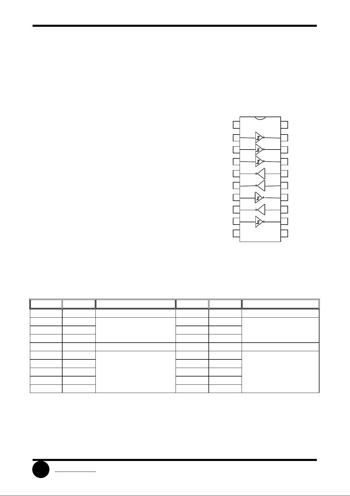
The SL75232N, SL75232D are monolithic device
containing 3 independent drives and 5 receivers. These are
designed to interface between date terminal equipment and
date communication equipment as designed by EIA-232-D.
Features
• Meets standard EIA-232-D (Revision of RS-232-C)
• Drivers
- Current Limited Output 10 mA Typical
- Power-off Output Impedance 300 Ω Min
- Slew Rate Control by Load Capacitor
- Flexible Supply Voltage Range
- Input Compatible with Most TTL and DTL Circuits
• Receivers
- Input Resistance 3 kΩ to 7 kΩ
- Input Signal Range ± 30 V
- Built -in Input Hysteresis (Double Threshold)
• 20 DIP/SO20: ÌS-001AD (SL75232N) / ÌS-013AÑ
(SL75232D)
Pin Description
Name Pin No Function Name Pin No Function
V
CC+
1 Driver Section Supply + V
CC-
10 Driver Section Supply DA1 16 DY1 5
DA2 15 DY2 6 Driver Output
DA3 13 Driver Input DY3 8
VCC 20 Receiver Section Supply GND 11 Ground
RA1 2 RY1 19
RA2 3 RY2 18
RA3 4 Receiver Input RY3 17 Receiver Output
RA4 7 RY4 14
RA5 9 RY5 12
V
CC-
RA5
DY3
RA4
DY2
DY1
RA3
RA2
RA1
V
CC+
10
9
8
7
6
5
4
3
2
1
11
12
13
14
15
16
17
18
19
20
GND
RY5
DA3
RY4
DA2
DA1
RY3
RY2
RY1
V
CC
Block Diagram
IL75232N, IL75232D
Page 2
SL75232
System Logic
Semiconductor SLS
Absolute Maximum Ratings
Symbol Parameter Rating Unit
V
CC+
Supply Voltage 15 V
V
CC-
Supply Voltage -15 V
VCC Supply Voltage 10 V
VI (Driver) Input Voltage
-15 ÷ +7
V
VI (Reciver) Input Voltage
± 30
V
VO (Driver) Output Voltage
-15 ÷ +15
V
PT Continuous Power Dissipation (Below 25 oC) 1.0 W
T
STG
Storage Temperature
-65 ÷ +175
o
C
Top Operating Temperature
0 ÷ +75
o
C
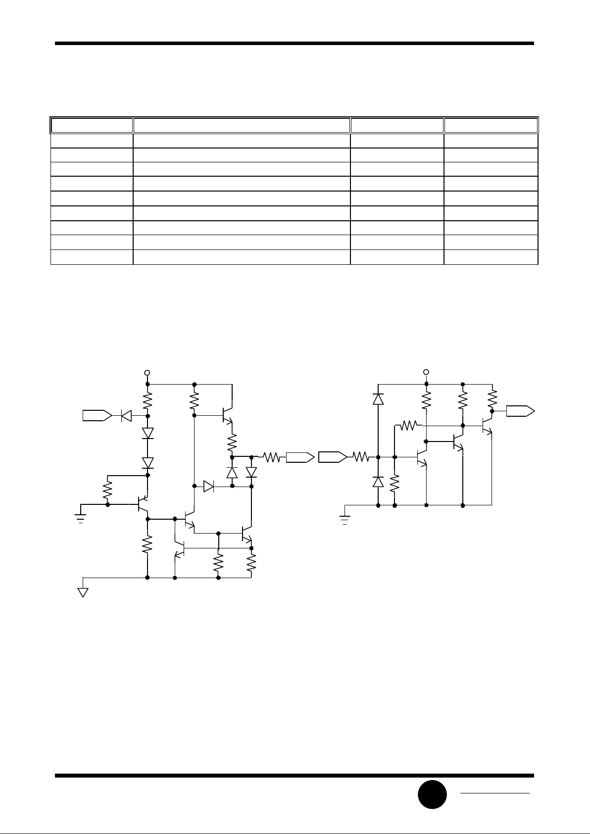
Schematic
V
CC-
300
70
6.2 Ê
8.2 Ê
70
7Ê
10Ê
3.6Ê
VCC+
DA
DY
DRIVER
RESEIVER
10 Ê
2 Ê
4 Ê
2 Ê
5 Ê9 Ê
V
CC
DA
DY
Page 3

SL75232
System Logic
Semiconductor
SLS
Electrical Characteristics
Supply Current
V
CC
= 5V, TA = 25 OC
Symbol Parameter Test Conditions Min Max Unit
I
CC+
Supply Current V
CC+
= 9 V VIN = 1.9V 15 mA
from V
CC+
No Load VIN = 0.8V 4.5
V
CC+
= 12 V VIN = 1.9V 19
No Load VIN = 0.8V 5.5
V
CC+
= 15 V VIN = 1.9V 25
No Load VIN = 0.8V 9
I
CC-
Supply Current V
CC-
= -9 V VIN = 1.9V -15 mA
from V
CC-
No Load VIN = 0.8V -3.2
V
CC-
= -12 V VIN = 1.9V -19
No Load VIN = 0.8V -3.2
V
CC-
= -15 V VIN = 1.9V -25
No Load VIN = 0.8V -3.2
ICC Supply Current VCC = 5 V VIN = 5.0V 30 mA
from VCC
Driver Section
Symbol Parameter Test Conditions Min Max Unit
VIH High Level V
CC+
= 9 V 1.9 V
Input Voltage V
CC-
= -9 V
VIL Low Level 0.8 V
Input Voltage
VOH High Level VIL = 0.8V V
CC+
= 9 V 6 V
Output Voltage
RL = 3 kΩ
V
CC-
= -9 V
V
CC+
= 13.2 V 9
V
CC-
= -13.2
V
VOL Low Level VIH = 1.9V V
CC+
= 9 V -6 V
Output Voltage
RL = 3 kΩ
V
CC-
= -9 V
V
CC+
= 13.2 V -9
V
CC-
= -13.2
V
IIH High Level VI = 5V 10
µA
Input Current
IIL Low Level VI = 0 -1.6 mA
Input Current
I
OS(H)
Short Circuit VI = 0.8V -6 -12 mA
Output Current VO = 0
at High Level
I
OS(L)
Short Circuit VI = 1.9V 6 12 mA
Output Current VO = 0
at Low Level
RO Output Resistance, V
CC+
= 0, V
CC-
= 0 300
Ω
Page 4

SL75232
System Logic
Semiconductor SLS
Power Off VO = -2V to 2V
Driver Switching Characteristic
V
CC+
= 9V, V
CC-
= -9V TA = 25 OC
Symbol Parameter Test Conditions Min Max Unit
t
PLH
Propagation Delay Time,
RL = 3 kΩ
500 ns
Low-To-High-Level Output
CL = 15 µF
t
PHL
Propagation Delay Time, 175 ns
High -To- Low -Level Output See Figure 1
t
TLH
Transition Time, 100 ns
Low-To-High-Level Output *
t
THL
Transition Time, 75 ns
High -To- Low -Level Output*
t
TLH
Transition Time,
RL = 3 kΩ to 7 kΩ
2.5
µs
Low-To-High-Level Output**
CL = 2500 ρF
(tip)
t
THL
Transition Time, 3.0
µs
High-To-Low -Level Output** See Figure 1 (tip)
*- Measured between 10 % and 90 % Points of Output Waveform
** - Measured between +3V and -3V Points on the Output Waveform (EIA-232-D Condition)
Receiver Section
Symbol Parameter Test Conditions Min Max Unit
VT+ Positive-Going 1.75 2.25 V
Threshold Voltage
VT- Negative-Going 0.75 1.25 V
Threshold Voltage
VOH High Level Output
VI= 0.75V, IOL=-0.5mA
2.6 5 V
Voltage Input Open, 2.6 5
IOL = -0.5 mA
VOL Low Level Output Voltage VI= 3V, IOL = 10 mA 0.45 V
IIH High-Level Input Current VI= 25V 3.6 8.3 mA
VI= 3V 0.43
IIL Low-Level Input Current VI= -25V -3.6 -8.3 mA
VI= -3V -0.43
IOS Short-Circuit -3 mA
Output Current (tip)
Receiver Switching Characteristic
VCC= 5V
Symbol Parameter Test Conditions Min Max Unit
t
PLH
Propagation Delay Time,
CL = 15 ρF
190 ns
Low-To-High-Level Output
RL = 3.9 kΩ
t
PHL
Propagation Delay Time,
CL = 15 ρF
60 ns
High -To- Low -Level Output
RL = 390 kΩ
t
TLH
Transition Time,
CL = 15 ρF
175 ns
Low-To-High-Level Output
RL = 3.9 kΩ
Page 5

SL75232
System Logic
Semiconductor
SLS
t
THL
Transition Time,
CL = 15 ρF
20 ns
High -To- Low -Level Output
RL = 390 kΩ
Parameter Measurement Information
DRIVER
CLRL
Test Circuit
OUTPUT
PULSE
GENERATOR
(See Note A)
RESEIVER
VCC
CL
R1
Test Circuit
OUTPUT
(See Note C)
PULSE
GENERATOR
(See Note A)
Voltage Waveform
INTPUT
50% 50%
1.5V
1.5V
3V
V
OL
V
OH
OV
10ns
t
PHL
t
PLH
t
TLH
t
THL
OUTPUT
TW=25 µs, Voltage Waveform
INTPUT
1.5V
1.5V
50%
10%10%
90%90%
50%
3V
V
OL
VOH
OV
10ns
t
PHL
tPLH
t
TLH
t
THL
OUTPUT
Note A. The pulse generator has the following characteristics. f = 200 KHz, ZO = 50 Ω
B. C included probe and jig capacitance.
C. All diodes are 1N3064 or equivalent.
Fig1. Propagation and Transition Times
Typical Application
DB95
SIO Card
ILA75232N,D
9
8
6
7
5
4
3
2
1
+5V
TX
CTS
DTR
RI
-12V
/RI
/DTR
SOUT
/CTS
RX
RTS
/RTS
SIN
DSR
DCD
+12V
/DCD
/DSR
UART
 Loading...