

SL74LV573
OCTAL D-TYPE TRANSPARENT LATCH (3-State)
By pinning SL74LV573 are compatible with SL74HC573 and
SL74HCT573 series. Input voltage levels are compatible with
stadard CMOS levels.
• Output voltage levels are compatible with input levels of CMOS,
NMOS and TTL ICS
• Voltage supply range from 1.2 to 5.5 V
• LOW input current: 1.0 µÀ; 0.1 µÀ at Ò = 25 °Ñ
• Output current 8 mÀ
• Latch current: not less than150 mÀ at Ò = 125 °Ñ
• ESD acceptable value: not less than 2000 V as per HBM and
not less than 200 V as per MM
FUNCTION TABLE
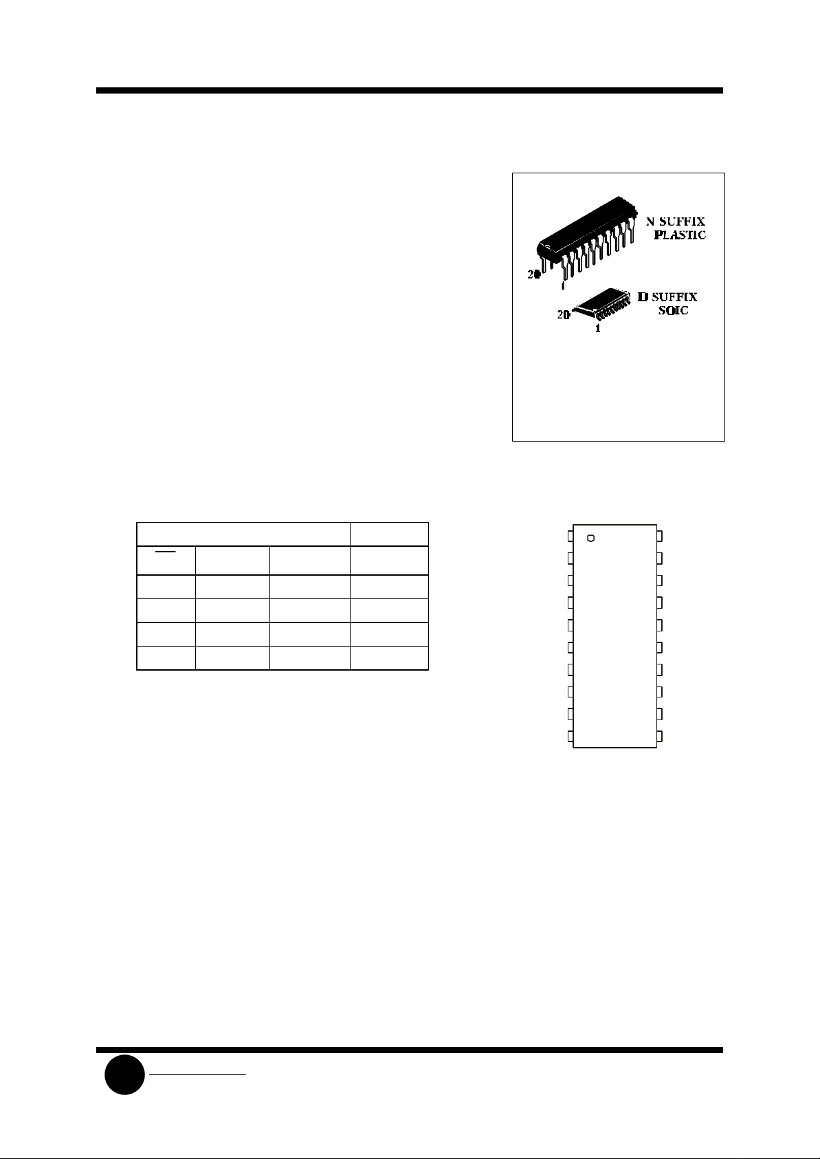
ORDERING INFORMATION
SL74LV573N Plastic DIP
SL74LV573D SOIC
TA = -40° to 125° C
for all packages
PIN ASSIGNMENT
Inputs Outputs
OE LE D Q
L H H H
L H L L
L L X no change
H X X Z
H -HIGH voltage level
L - LOW voltage level
X - don’t care
Z - High impedance state
OE
D0
D1
D2
D3
D4
D5
D6
D7
GND
1
2
3
4
5
6
7
8
9
10
20
19
18
17
16
15
14
13
12
11
V
Q0
Q1
Q2
Q3
Q4
Q5
Q6
Q7
LE
CC
System Logic
SLS
Semiconductor
SL74LV573
ABSOLUTE MAXIMUM RATINGS
Symbol Parameter Rating Unit Conditions
Vcc Supply voltage -0.5 to +7.0 V
Iik, Input diode current ±20 mA VI<-0.5 V or VI>Vcc>+0.5 V
Iok Output diode current ±50 mA V0<-0.5 V or VI>Vcc>+0.5 V
Io Output current bus drivers ±35 mA -0.5 V<Vo<Vcc+0.5 V
Icc DC Vcc or GND current for types
bus driver outputs
I
GND current ±50 mÀ
GND
Tstg Storage temperature range -65 to +150
PD Power dissipation per package:
DIP
SO
Notes:
Power dissipation value decreases for:
DIP - 12 mW°C the range from 70 to 125°Ñ
SO - 8 mW°C the range from 70 to 125°Ñ
±70
750
500
mA
î
Ñ
mW
RECOMMENDED OPERATING CONDITIONS
Symbol Parameter Min Max Unit Conditions
Vcc Supply voltage 1.0 5.5 V
VI Input voltage 0 Vcc V
Vî Output voltage 0 Vcc V
T Operating temperature range -40 +125
tr,tf Input rise and fall times 500
200
100
50
Note - The IC function down to Vññ = 1.0 V (input levels - VIL=0 V, VIH=Vcc); DC characterisics are
guaranteed at Vcc=1.2 ÷ 5.5 V.
o
C
ns/V Vcc= 1.0 ÷ 2.0 V
Vcc= 2.0 ÷ 2.7 V
Vcc= 2.7 ÷ 3.6 V
Vcc= 3.6 ÷ 5.5 V
System Logic
SLS
Semiconductor

SL74LV573
DC CHARACTERISTICS
Sym Conditions Limits
bol Parameter Vcñ VI -40 to +25°C +85 îÑ +125 îÑ Unit
(V) Min Max Min Max Min Max
VIH HIGH level
input voltage
VIL LOW level
output
voltage
VOH HIGH level
output
voltage
VOH HIGH level
output
voltage; BUS
driver outputs
VOL LOW level
output
voltage
1.2
2.0
2.7 to 3.6
4.5 to 5.5
1.2
2.0
2.7 to 3.6
4.5 to 5.5
1.2
2.0
2.7
3.6
5.5
3.0
4.5
1.2
2.0
2.7
3.6
5.5
0.9
1.4
2.0
0.7 Vcc
-
-
-
-
V
IO =-100 µÀ 1.05
IH
or
VIL
V
IO =-8 mA
IH
or
IO =-16 mA
VIL
V
IO =100µÀ -
IH
or
VIL
1.85
2.55
3.45
5.35
2.48
3.70
-
-
-
-
-
-
-
-
0.3
0.6
0.8
0.3 Vcc
-
-
-
-
-
-
-
0.15
0.15
0.15
0.15
0.15
0.9
1.4
2.0
0.7 Vcc
-
-
-
-
1.0
1.8
2.5
3.4
5.3
2.40
3.60
-
-
-
-
-
-
-
-
-
0.3
0.6
0.8
0.3 Vcc
-
-
-
-
-
-
-
0.2
0.2
0.2
0.2
0.2
0.9
1.4
2.0
0.7 Vcc
-
-
-
-
1.0
1.8
2.5
3.4
5.3
2.20
3.50
-
-
-
-
-
-
-
-
--
0.3
0.6
0.8
0.3 Vcc
-
-
-
-
-
-
-
0.2
0.2
0.2
0.2
0.2
V
V
V
V
V
VOL LOW level
voltage; BUS
driver outputs
II Input leakage
current
IOZ OFF-state
current
Icc Supply
current
Icc Additional
supply
current per
input
SLS
System Logic
Semiconductor
3.0
4.5
5.5 Vññ
5.5 V
5.5 Vññ
2.7 äî 3.6 VI = Vcc-0.6V - 0.2 0.5 - 0.85 mA
V
IO =8 mA
IH
or
IO =16 mA
VIL
- ±1.0 ±1.0 - ±1.0 µÀ
or
GND
- ±0.5 ±5.0 - ±10.0 µÀ
IH
or
VIL
Io = 0 8.0 80 160 µÀ
or
GND
-
0.33
-
0.40
-
0.40
-
0.55
-
0.50
-
0.65
V

SL74LV573
AC CHARACTERISICS (C
Sym Conditions Limits
=50 pF, RL=1 KΩ, tLH = tHL = 2.5 ns)
L
bol Parameter Vcc -40 to +25°C
Min Max Min Max Min Max
t
Propagation
PHL/PLH
t
Propagation
PHL/PLH
t
3-state
PZH/PZL
t
3-state
PHZ/PLZ
delay Dn to
Qn
delay LE to
Qn
output enable
time OE to
Qn
outpiut
disable time
OE to Qn
1.2
2.0
2.7
3.0
4.5
1.2
2.0
2.7
3.0
4.5
1.2
2.0
2.7
3.0
4.5
1.2
2.0
2.7
3.0
4.5
VI = Vcc or
GND
VI = Vcc or
GND
VI = Vcc or
GND
VI = Vcc or
GND
-
150
-
30
-
23
-
18
-
15
-
160
-
34
-
28
-
20
-
17
-
140
-
28
-
22
-
17
-
14
-
160
-
31
-
23
-
20
-
17
+85°C +125°C Unit
-
160
-
39
-
29
-
23
-
19
-
180
-
43
-
31
-
25
-
21
-
160
-
37
-
28
-
22
-
18
-
160
-
39
-
29
-
24
-
20
-
170
-
49
-
36
-
29
-
24
-
190
-
53
-
34
-
31
-
26
-
170
-
48
-
35
-
28
-
23
-
170
-
48
-
36
-
29
-
24
ns
ns
ns
ns
tW LE pulse
tsu Setup time
th Hold time Dn
CI Input
CPD Power
width HIGH
Dn to LE
to LE
capacitance
dissipation
capacitance
per package
1.2
2.0
2.7
3.0
4.5
1.2
2.0
2.7
3.0
4.5
1.2
2.0
2.7
3.0
4.5
5.0 Ò=+25 îÑ 7.0 - ns
5.5 Ò=+25 îÑ
100
29
21
17
15
50
15
11
8
6
40
8
8
8
8
52 - ns
VI = Vcc or
GND
-
125
-
34
-
25
-
20
-
18
-
75
-
17
-
13
-
10
-
-
-
-
-
-
8
40
8
8
8
8
-
150
-
41
-
30
-
24
-
21
-
100
-
20
-
15
-
12
-
10
-
40
-
-
-
-
8
8
8
8
-
ns
-
-
-
-
-
ns
-
-
-
-
-
ns
-
-
-
-
System Logic
SLS
Semiconductor

SL74LV573
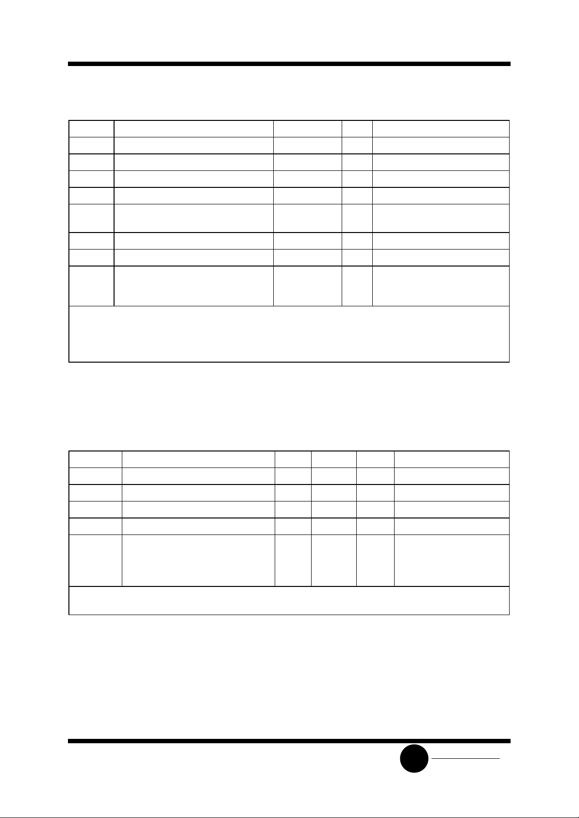
1.9 mm
18
19
20
1.51 mm
1
2
3
Drawing of the chip
15
1617
On-chip marking
74LV573/574
4
5
6 7
1314
12
11
10
9
8
Pads allocation Table
coordinates (counted from lower left corner), mm Pad
number
01 0.128 0.545 0.108 x 0.108
02 0.128 0.229 0.108 x 0.108
03 0.330 0.120 0.108 x 0.108
04 0.576 0.120 0.108 x 0.108
05 0.738 0.120 0.108 x 0.108
06 1.054 0.120 0.108 x 0.108
07 1.216 0.120 0.108 x 0.108
08 1.466 0.120 0.108 x 0.108
09 1.682 0.314 0.108 x 0.108
10 1.682 0.533 0.108 x 0.108
11 1.682 0.839 0.108 x 0.108
12 1.682 1.108 0.108 x 0.108
13 1.422 1.274 0.108 x 0.108
14 1.149 1.274 0.108 x 0.108
15 0.971 1.274 0.108 x 0.108
16 0.811 1.274 0.108 x 0.108
17 0.633 1.274 0.108 x 0.108
SLS
System Logic
Semiconductor
X
Y
Pad size, mm

SL74LV573
18 0.360 1.274 0.108 x 0.108
19 0.128 1.108 0.108 x 0.108
20 0.128 0.854 0.108 x 0.108
System Logic
SLS
Semiconductor
 Loading...