

Page 1
THIS DOCUMENT IS FOR MAINTENANCE
PURPOSES ONLY AND IS NOT
RECOMMENDED FOR NEW DESIGNS
Page 2
FEATURES
Can be Muted with High or Low State inputs
Operational Amplifier Configuration
Works Over Wide Voltage Range
APPLICATIONS
Audio Amplifier for Portable Receivers
Power Op. Amp
High Level Active Filter
QUICK REFERENCE DATA
Supply Voltage: 4.5V to 13.6V
Voltage Gain: 70dB
Output into 8Ω on 9V Supply : 400mW (min.)
ABSOLUTE MAXIMUM RATINGS
Supply voltage: 15V
Storage temperature: —55°C to + 125°C
SL6310C
500mW SWITCHABLE AUDIO AMPLIFIER/OP AMP
The SL6310C is a low power audio amplifier which can be
switched off by applying a mute signal to the appropriate pin.
Despite the low quiescent current consumption of 5mA (only
0.6mA when muted) a minimum output power of 400mW is
available into an 8Ω load from a 9V supply.
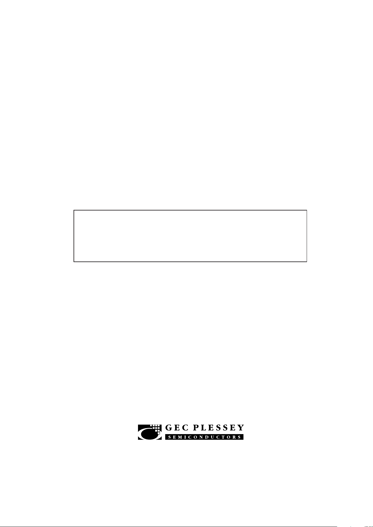
MP8
DG8
DP8
Fig. 1 Pin connections, SL6310 - (top view)
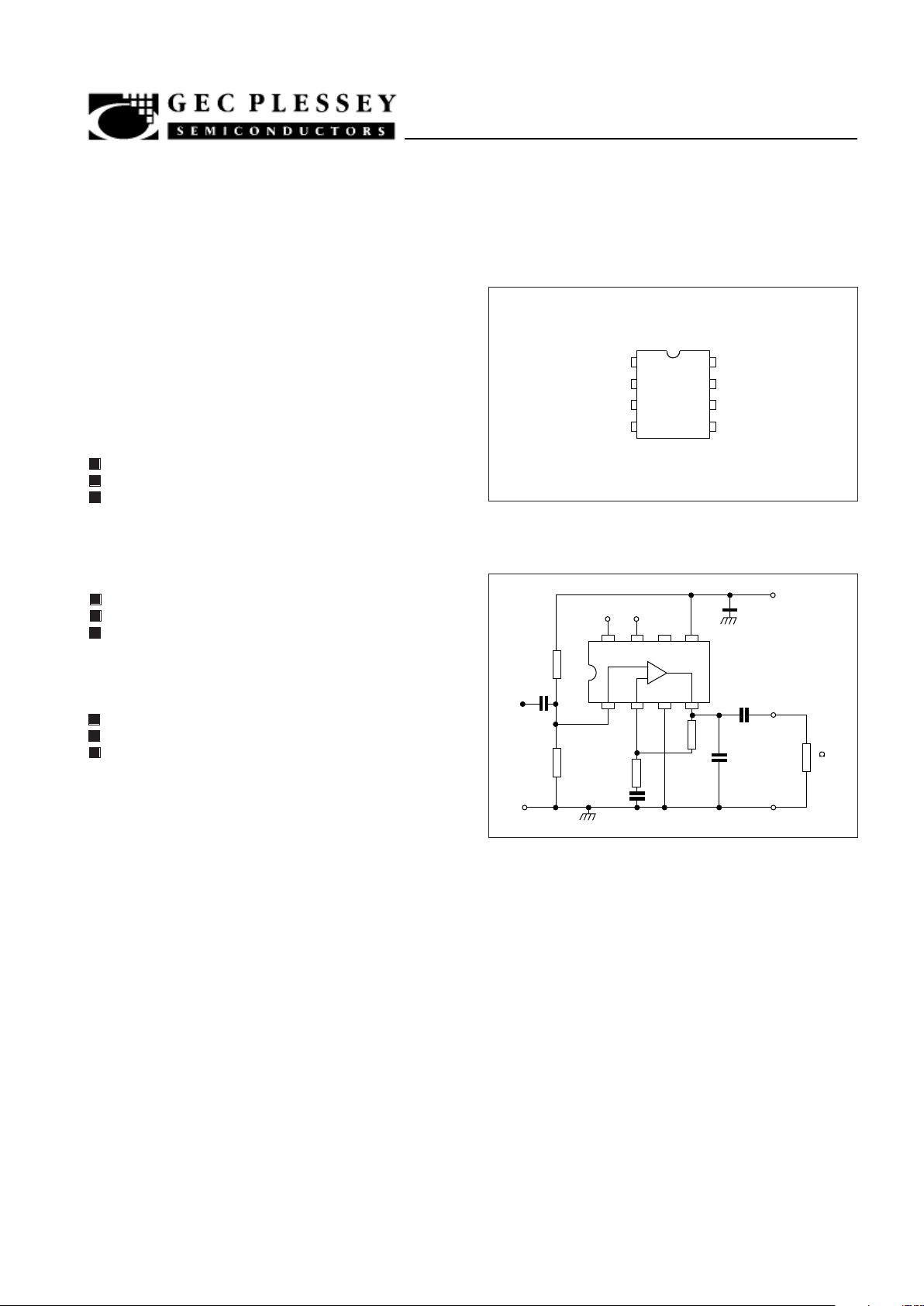
Fig. 2 SL6310 Test Circuit
DS 3302 -1
1
2
3
4
8
7
6
5
NON INV. INPUT
INV. INPUT
EARTH
OUTPUT
MUTE "B"
MUTE "A"
NC
V
CC
SL6310
MUTE B MUTE A
100n
R1
220k
8765
1234
INPUT
+
-
V
CC
100µ
OUTPUT
EARTH
R4
120k
1µ
220n
100µ
R3
4.7k
R2
220k
8
LOAD
Page 3

SL6310C
OPERATING NOTES
Mute facility
The SL6310 has two mute control pins to allow easy
interfacing to inputs of high or low levels. Mute control ‘A’, pin
7, is left open circuit or connected to a voltage within 0.65 volt
of Vcc (via a 100kΩ resistor) for normal operation. When the
voltage on pin 7 is reduced to within 1 volt of earth (via a 100kΩ
resistor) the SL6310 is muted
Audio amplifier
AstheSL6310 is an operational amplifier it is easy to obtain
the voltage gain and frequency response required. To keep
the input impedance high it is wise to feed the signal to the non-
inverting input as shown in Fig.2. In this example the input
impedance is approximately 100kΩ. The voltage gain is
determined by the ratio (R3 + R4)/R3 and should be between
3 and 30 for best results. The capacitor in series with R3,
together with the input and output coupling capacitors,
determines the low frequency rolloff point. The upper
frequency limit is set by the device but can be restricted by
connecting a capacitor across R4.
Operational amplifier
It is impossible to list all the application possibilities in a
single data sheet but the SL6310 offers considerable
advantages over conventional devices in high output current
applications such as lamp drivers (Fig.3) and servo amplifiers
(Fig.4) .
Buffer and output stages for signal generators are another
possibility together with active filter sections requiring high
output current.
NOTE
1. The input bias current flows out of pins 1 and 2 due to PNP input stage
Typ.
5.0
0.55
0.6
2
50
0.2
70
2.1
10.6
60
500
0.4
Min.
40
40
400
Value
Characteristics
Units
Conditions
Supply current
Supply current mute (A)
Supply current mute (B)
Input offset voltage
Input offset current
Input bias current (Note 1)
Voltage gain
Input voltage range
CMRR
Output power
THD
Max.
7.5
1
0.9
20
500
1
3
mA
mA
mA
mV
nA
µA
dB
V
V
dB
mW
%
Pin 7 via 470k to earth
Pin 8 = V
CC
RS ≤ 10k
VCC = 4.5V
V
CC
= 13V
R
S
≤10K
R
L
= 8Ω
P
OUT
= 400mW,
Gain = 28dB
Fig. 3 SL6310 lamp driver
Fig. 4 SL6310 servo amplifier
ELECTRICAL CHARACTERISTICS
Test conditions (unless otherwise stated):
Supply voltage Vcc: 7V
Ambient temperature: -30°C to +85°C
Mute facility : Pins 7 and 8 open circuit frequency = 1kHz
Page 4

SL6310C
Fig. 5 Gain v. frequency
Fig. 6 Gain v. supply voltage
Fig. 8 Output power v. supply voltage at 5% (max) distortionFig. 7 Supply current v. supply voltage
80
60
40
20
100 1k 10k 100k
FREQUENCY
(Hz)
GAIN (dB)
74
72
70
68
66
64
62
4 8 12 10
VOLTAGE (V)
GAIN (dB)
1500
1000
500
0
04 8
CURRENT IN NON - MUTED STATE (mA)
12
MUTE B
MUTE A
NON - MUTED
CURRENT IN MUTED STATE (µA)
2
0
6
4
VOLTAGE
(V)
MUTE B : PIN 8 TO SUPPLY
MUTE A : PIN 7 TO EARTH BY 100k RESISTOR
1.2
0.8
0.4
0
04 812
OUTPUT POWER (W)
VOLTAGE (V
)
4 LOAD
8
LOAD
16 LOAD
 Loading...