

Page 1

SL6619
Direct Conversion FSK Data Receiver
Preliminary Information
Supersedes July 1996 version, DS3853 - 3.5 DS3853 - 4.1 April 1998
The SL6619 is an advanced Direct Conversion FSK Data
Receiver for operation up to 450 MHz. The device integrates all
functions to convert a binary FSK modulated RF signal into a
demodulated data stream.
Adjacent channel rejection is provided using tuneable gyrator
filters. RF and audio AGC functions assist operation when large
interfering signals are present and an automatic frequency control
(AFC) function is provided to extend centre frequency acceptance.
FEATURES
■ Very Low Power Operation from Single Cell
■ Superior Sensitivity
■ Operation at 512, 1200 and 2400 Baud
■ On Chip 1 Volt Regulator
■ 1mm Height Miniature Package
■ Automatic Frequency Control Function
■ Programmable Post Detection Filter
■ AGC Detection Circuitry
■ Power Down Function
■ Battery Strength Indicator
GTH ADJ
32 31 30 29 28 27 26 25
IRF
GND
MIXIP A
MIX DEC
MIXIP B
REG CNT
V
REG
TPI
1
2
3
4
5
6
7
8
9 10111213141516
I1
Fig. 1 Pin identification diagram (top view). See Table 1 for
pin descriptions
TC ADJ
IAGC OP
TP LIM I
SL6619
1
I2
CC
V
LOIP I
BATT
V
BRF1
GYR I
LOIP Q
BRF CNT
AFC2
24
23
22
21
20
19
18
17
Q1
Q2
AFC1
BATT FLAG
VCC2
DATA OP
BEC
AFC OP
V
REF
TPQ
TP32
APPLICATIONS
■ Pagers, including Credit Card, PCMCIA and
Watch Pagers
■ Low Data Rate Receivers, e.g. Security Systems
ORDERING INFORMATION
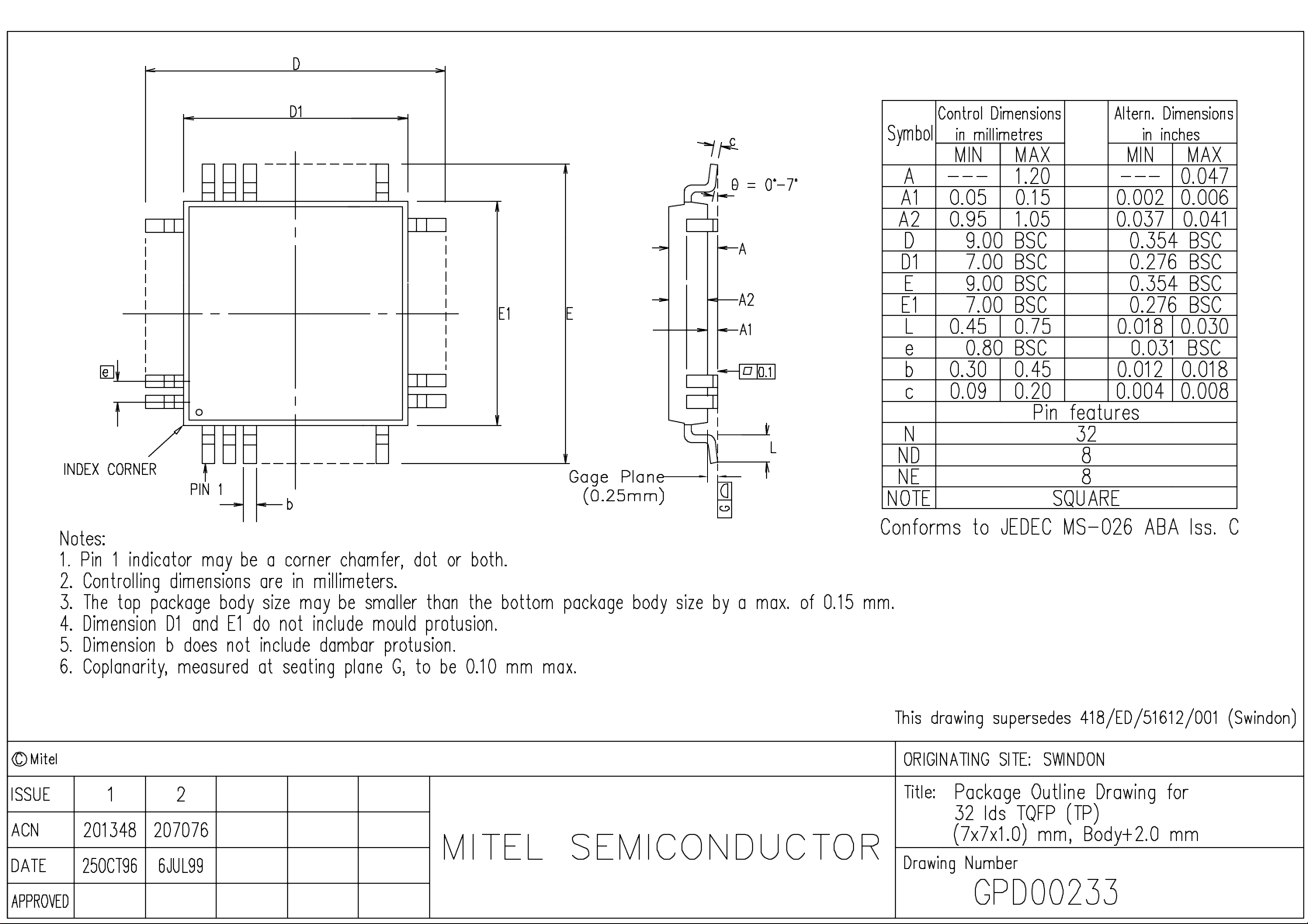
SL6619/KG/TP1N 1mm TQFP device, baked and dry
packed, supplied in trays
SL6619/KG/TP1Q 1mm TQFP device, baked and dry
3
5
packed, supplied in tape and reel
12 9
MIXER
10 13 7 6 8 29 4 20 11 22 2 18
−
+
1·0V
−
1·08V
+
ABSOLUTE MAXIMUM RATINGS
Storage temperature
Operating temperature
Maximum voltage on any pin w.r.t. any
other pin, subject to the following conditions:
Current, pin 3 (MIXIP), pin 5 (MIXPB),
pin 12 (LOIPI) and pin 14 (LOIPB)
Most negative voltage on any pin
MIX
LIMITER
BEC VCC1 VCC2 GND V
DEC
4
f
DETECTOR
LIMITER
AFC
REF
255°C to1150°C
210°C to155°C
14V
<5ma
20·5V w.r.t. gnd
26
27
21
31
30
19
14 15 16 28 23 17 1 32 24 25
Fig. 2 Block diagram of SL6619
Page 2

SL6619
Pin number
1
2
3
4
5
6
7
8
9
10
11
12
13
14
Pin name
IRF
GND
MIXIP A
MIX DEC
MIXIP B
REG CNT
VREG
TPI
I1
I2
VCC1
LOIP I
GYRI
LOIP Q
Pin description
LNA current source
Ground
Mixer input A
Mixer biasing decouple
Mixer input B
1V regulator control external PNP drive
1V regulator output voltage
I channel pre-gyrator filter test point.
Mixer output, I channel
Mixer output, I channel
Positive supply 1
LO input channel I
Gyrator current adjust pin
LO input channel Q
15
16
17
18
19
20
21
22
23
24
25
26
27
28
29
30
Q1
Q2
TPQ
VREF
AFC OP
BEC
DATA OP
VCC2
BATT FLAG
AFC1
AFC2
BRF CNT
BRF1
VBATT
TP LIM I
IAGC OP
Mixer output, Q channel
Mixer output, Q channel
Q channel pre-gyrator filter test point
Reference voltage
AFC output
Battery economy control
Data output pin
Positive supply 2
Battery flag output
AFC characteristic defining pin
AFC characteristic defining pin
Bit rate filter control
Bit rate filter 1, output from detector
Battery flag input voltage
I channel limiter (post gyrator filter) test point, output only
Audio AGC output current
31
32
TC ADJ
GTH ADJ
Audio AGC time constant adjust
Audio AGC gain and threshold adjust. RSSI signal indicator
Table 1 SL6619 pin descriptions
2
Page 3

ELECTRICAL CHARACTERISTICS (1)
Electrical Characteristics (1) are guaranteed over the following range of operating conditions unless otherwise stated
T
= 125°C, VCC1 = 1·3V, VCC2 = 2·7V
AMB
Value
Characteristic
Pin
Min.
Typ. Max.
ConditionsUnits
SL6619
Supply voltage, VCC1
Supply voltage, V
Supply current, I
Supply current, I
1 volt regulator, V
CC
CC
CC
1
2
REG
2
1 volt regulator load current
LNA current source, IRF
Reference voltage, V
V
source current
REF
V
sink current
REF
REF
Data Amplifier
DATA OP sink current
DATA OP leakage current
Output mark:space ratio
Battery Economy
Power down I
Power down I
CC
CC
1
2
BEC input logic high
BEC input logic low
BEC input current
BEC input current
11
22
11
22
18
18
18
21
21
21
11
22
20
20
20
20
0·95
1·9
1·20
260
7
7
1
0·95
0·25
375
1·15
1·3
2·7
1·60
350
1·0
500
1·25
25
7:9
2·7
3·5
2·2
460
1·05
3
700
1·31
20
1·0
1·0
9:7
VCC1<VCC220·8V
V
V
mA
Including IRF
µA
V
mA
µA
V
= 3mA, external PNP(b>100, V
I
LOAD
External PNP (h
>100, V
FE
CE
PTAT, voltage on pin 1 = 0·3V and 1·3V
Typical temperature coefficient = 10·1mV/°C
µA
µA
µA
Output logic low, pin 21 voltage = 0·3V
µA
Output logic high, pin 21 voltage = V
Preamble at 1200 baud, Df = 4kHz,
= 0·1V)
CE
CC
= 0·1V)
2
pin 26 = 0V, BRF capacitor = 560pF,
DATA OP pullup resistor = 200kΩ
V
220·3V
CC
21·0
21·0
V
10
10
CC
0·3
0·5
2·0
0
1·0
1·0
µA
Pin 20 = logic low
µA
Pin 20 = logic low
V
V
µA
µA
Powered up
Powered down
Powered up
Powered down
2
Battery Flag
V
trigger point
BATT
BATT FLAG sink current
BATT FLAG sink current
BATT FLAG sink current
V
input voltage
BATT
V
input current
BATT
V
input current
BATT
28
23
23
23
28
28
28
1·04
1·0
25
21·0
21·0
1·08
1·12
1·0
2·0
1·0
1·0
V
Current sunk by pin 23 = 1µA
µA
Pin 28 voltage = 1·04V
µA
Pin 28 voltage = 1·12V
µA
Pin 28 voltage = 1·14V
V
µA
V
= 1·14V
BATT
µA
V
= 1·04V
BATT
Continued…
3
Page 4

SL6619
ELECTRICAL CHARACTERISTICS (1) (Cont.)
Electrical Characteristics (1) are guaranteed over the following range of operating conditions unless otherwise stated
T
= 125°C, VCC1 = 1·3V, VCC2 = 2·7V
AMB
Value
Characteristic
Mixers
LO DC bias voltage
Gain to TPI
Gain to TPQ
Match of gain to TPI
and TPQ
Audio AGC
IAGC OP max. sink current
IAGC OP leakage current
AFC
AFC DC current, I
AFC4k5
AFC DC current
AFC DC current
Pin
12,14
3,5,8,12
3,5,14,
17
3,5,8,
12,14,17
30
30
19
19
19
Min.
38
38
21
I
AFC4k5
10·2
Typ.
V
CC
42
42
0
40
0·0
I
AFC4k5
10·7
I
AFC4k5
20·9
Max.
1
46
Units
V
dB
LO inputs (12, 14) driven in quadrature:
45mVrms at 450MHz, CW.
Mixer inputs (3, 5) driven differentially:
0·45mVrms at 450·004MHz, CW.
46
11
1
I
AFC4k5
dB
dB
µA
µA
µA
µA
µA
As gain to TPI
As gain toTPI
TPI, TPQ signals limiting
No signal applied
f
= fLO14·5kHz, CW
C
f
= fLO12·5kHz, CW
C
= fLO16·5kHz, CW
f
C
20·2
Conditions
Bit Rate Filter Control
BRF CNT input logic high
BRF CNT input logic low
Tristate I/P current window
BRF 1 output current
BRF 1 output current
BRF 1 output current
BRF CNT input high current
BRF CNT input low current
26
26
26
27
27
27
26
26
V
CC
20·3
0
20·4
27·5
27·5
V
2
VCC2
0·1
10·4
3·5
1·7
0·74
17·5
17·5
µA
µA
µA
µA
µA
µA
2400 baud
V
1200 baud
512 baud
Pin 26 logic high
Pin 26 logic low
Pin 26 logic tristate (open circuit)
4
Page 5

ELECTRICAL CHARACTERISTICS (2)
Electrical Characteristics (2) are guaranteed over the following range of operating conditions unless otherwise stated.
Characteristics are tested at room temperature only and are guaranteed by characterisation test or design.
T
= 210°C to 155°C, VCC1 = 1·4V to 2·0V, VCC2 = 2·3V to 3·2V. VCC1,VCC220·8V
AMB
Value
Characteristic
Pin
Min.
Typ. Max.
ConditionsUnits
SL6619
Supply voltage, VCC1
Supply voltage, V
Supply current, I
Supply current, I
1 volt regulator, V
CC
CC
CC
1
2
REG
2
1 volt regulator load current
LNA current source, IRF
Reference voltage, V
V
source current
REF
V
sink current
REF
REF
Turn-on time
Turn-off time
Data Amplifier
DATA OP sink current
DATA OP leakage current
Output mark:space ratio
Battery Economy
Power down I
Power down I
CC
CC
1
2
BEC input logic high
BEC input logic low
BEC input current
BEC input current
11
22
11
22
18
18
18
21
21
21
11
22
20
20
20
20
0·95
1·9
1·3
2·7
1·60
350
7
7
1
0·93
0·25
375
1·13
1·0
500
1·25
22
7:9
2·7
3·5
2·4
510
1·05
3
800
1·33
18
0·8
5
1
1·5
9:7
VCC1<VCC220·8V at >25°C only
V
V
mA
Including IRF
µA
V
mA
µA
V
= 3mA, external PNP(b>100, V
I
LOAD
External PNP(h
>100, V
FE
CE
PTAT, voltage on pin 1 = 0·3V and 1·3V
Typical temperature coefficient = 10·1mV/°C
µA
µA
ms
Stable data O/P when 3dB above sensitivity.
C
= 2·2µF
VREF
ms
Fall to 10% of steady state I
µA
Output logic low, pin 21 voltage = 0·3V
µA
Output logic high, pin 21 voltage = V
Preamble at 1200 baud, Df = 4kHz,
= 0·1V)
1. C
CC
VREF
CC
= 0·1V)
CE
= 2·2µF
2
pin 26 = 0V, BRF capacitor = 560pF,
DATA OP pullup resistor = 200kΩ
V
220·3V
CC
21·0
21·0
V
12
12
CC
0·3
0·5
2·0
0
1·5
1·5
µA
Pin 20 = logic low
µA
Pin 20 = logic low
V
V
µA
µA
Powered up
Powered down
Powered up
Powered down
2
Battery Flag
V
trigger point
BATT
BATT FLAG sink current
BATT FLAG sink current
BATT FLAG sink current
V
input voltage
BATT
V
input current
BATT
V
input current
BATT
28
23
23
23
28
28
28
1·04
2
20
21·5
21·5
1·08
1·12
2
2·0
1·5
1·5
V
Current sunk by pin 23 = 1µA
µA
Pin 28 voltage = 1·04V
µA
Pin 28 voltage = 1·12V
µA
Pin 28 voltage = 1·14V
V
µA
V
= 1·14V
BATT
µA
V
= 1·04V
BATT
Continued…
5
Page 6

SL6619
ELECTRICAL CHARACTERISTICS (2) (Cont.)
Electrical Characteristics (2) are guaranteed over the following range of operating conditions unless otherwise stated.
Characteristics are tested at room temperature only and are guaranteed by characterisation test or design.
T
= 210°C to 155°C, VCC1 = 1·4V to 2·0V, VCC2 = 2·3V to 3·2V. VCC1,VCC220·8V
AMB
Value
Characteristic
Mixers
LO DC bias voltage
Gain to TPI
Gain to TPQ
Match of gain to TPI
and TPQ
Audio AGC
IAGC OP max. sink current
IAGC OP leakage current
Pin
12,14
3,5,8,12
3,5,14,
17
3,5,8,
12,14,17
30
30
Min.
35
35
21·5
15
Typ.
V
CC
42
42
0
40
Max.
1
46
Units
V
dB
LO inputs (12, 14) driven in quadrature:
45mVrms at 450MHz, CW.
Mixer inputs (3, 5) driven differentially:
0·45mVrms at 450·004MHz, CW.
46
11·5
80
2
dB
dB
µA
µA
As gain to TPI
As gain toTPI
TPI, TPQ signals limiting
No signal applied
Conditions
AFC
AFC DC current, I
AFC4k5
AFC DC current
AFC DC current
Bit Rate Filter Control
BRF CNT input logic high
BRF CNT input logic low
Tristate I/P current window
BRF 1 output current
BRF 1 output current
BRF 1 output current
BRF CNT input high current
BRF CNT input low current
19
19
19
26
26
26
27
27
27
26
26
I
AFC4k5
10·1
V
CC
20·3
0
20·4
210
210
0·0
I
AFC4k5
µA
µA
f
= fLO14·5kHz, CW
C
f
= fLO12·5kHz, CW
C
10·7
I
AFC4k5
20·9
2
I
AFC4k5
20·1
VCC2
0·1
10·4
3·5
1·7
0·74
110
110
µA
V
V
µA
µA
µA
µA
µA
µA
= fLO16·5kHz, CW
f
C
2400 baud
1200 baud
512 baud
Pin 26 logic high
Pin 26 logic low
Pin 26 logic tristate (open circuit)
6
Page 7

SL6619
RECEIVER CHARACTERISTICS (450MHz)
Receiver Characteristics (450MHz) are guaranteed over the following range of operating conditions unless otherwise stated.
Characteristics are not tested but are guaranteed by characterisation test or design. All measurements made using the
characterisation circuit Fig. 5. See Application Note AN137 for details of test method.
T
= 210°C to 155°C, VCC1 = 1·04V to 2·0V, VCC2 = 2·3V to 3·2V, VCC1,VCC220·8V, carrier frequency = 450MHz,
AMB
BER = 1 in 30, AFC open loop. LNA gain set such that an RF signal of273dBm at the LNA input, offset from the LO
by 4kHz, gives a typical IF signal level of 300mV p-p at TPI and TPQ. LNA noise figure,2dB
Value
Characteristic
Min.
Typ.
Max.
Units
Conditions
Sensitivity
Intermodulation, IP3
Adjacent Channel
Deviation Acceptance
Up
Down
Up
Down
Up
Down
Centre Frequency Acceptance
50
48
62·5
60
11·8
22·7
11·7
23
62·0
62·0
2128
2126
2123
57
55
53
74
72
69
11·9
22·5
13·0
22·3
12·5
22·3
62·8
62·5
62·5
2122
2119
14·6
21·7
14·6
21·7
62·9
63·2
dBm
dBm
dBm
dB
dB
dB
dB
dB
dB
kHz
kHz
kHz
kHz
kHz
kHz
kHz
kHz
kHz
512bps, Df = 4·5kHz
1200bps, Df = 4·0kHz
2400bps, Df = 4·5kHz. LO = 215dBm
512bps, Df = 4·5kHz
1200bps, Df = 4·0kHz
2400bps, Df = 4·5kHz. LO = 215dBm. Channel
spacing 25kHz
512bps, Df = 4·5kHz
1200bps, Df = 4·0kHz
2400bps, Df = 4·5kHz. LO = 215dBm. Channel
spacing 25kHz
512bps, Df = 4·5kHz, no AFC
512bps, Df = 4·5kHz, no AFC
1200bps, Df = 4·0kHz, no AFC
1200bps, Df = 4·0kHz, no AFC
2400bps, Df = 4·5kHz, no AFC
2400bps, Df = 4·5kHz, no AFC
512bps, Df = 4·5kHz, no AFC
1200bps, Df = 4·0kHz, no AFC
2400bps, Df = 4·5kHz, no AFC
AFC Capture Range (AFC
Closed Loop)
64
63·5
64
kHz
kHz
kHz
512bps, Df = 4·5kHz. All at sensitivity 13dB or above
1200bps, Df = 4·0kHz. All at sensitivity 13dB or above
2400bps, Df = 4·5kHz. All at sensitivity 13dB or above
7
Page 8

SL6619
RECEIVER CHARACTERISTICS (280MHz)
Receiver Characteristics (280MHz) are guaranteed over the following range of operating conditions unless otherwise stated.
Characteristics are not tested but are guaranteed by characterisation test or design. All measurements made using the
characterisation circuit Fig. 5. See Application Note AN137 for details of test method.
T
= 210°C to 155°C, VCC1 = 1·04V to 2·0V, VCC2 = 2·3V to 3·2V, VCC1,VCC220·8V, carrier frequency = 280MHz,
AMB
BER = 1 in 30, AFC open loop. LNA gain set such that an RF signal of273dBm at the LNA input, offset from the LO
by 4kHz, gives a typical IF signal level of 300mV p-p at TPI and TPQ. LNA noise figure,2dB
Value
Characteristic
Min.
Typ.
Max.
Units
Conditions
Sensitivity
Intermodulation, IP3
Adjacent Channel
Deviation Acceptance
Up
Down
Up
Down
Up
Down
Centre Frequency Acceptance
2128
2127
52
49
62·5
60
11·8
22·7
11·7
23·0
62·0
62·0
2129
2127
2124
57
56
53·5
74
72
70
11·9
22·5
13·0
22·3
12·5
22·3
62·8
62·5
62·5
2124
2121
60
57
80
77
14·6
21·7
14·6
21·7
62·9
63·2
dBm
dBm
dBm
dB
dB
dB
dB
dB
dB
kHz
kHz
kHz
kHz
kHz
kHz
kHz
kHz
kHz
512bps, Df = 4·5kHz
1200bps, Df = 4·0kHz
2400bps, Df = 4·5kHz. LO = 215dBm
512bps, Df = 4·5kHz
1200bps, Df = 4·0kHz
2400bps, Df = 4·5kHz. LO = 215dBm. Channel
spacing 25kHz
512bps, Df = 4·5kHz
1200bps, Df = 4·0kHz
2400bps, Df = 4·5kHz. LO = 215dBm. Channel
spacing 25kHz
512bps, Df = 4·5kHz, no AFC
512bps, Df = 4·5kHz, no AFC
1200bps, Df = 4·0kHz, no AFC
1200bps, Df = 4·0kHz, no AFC
2400bps, Df = 4·5kHz, no AFC
2400bps, Df = 4·5kHz, no AFC
512bps, Df = 4·5kHz, no AFC
1200bps, Df = 4·0kHz, no AFC
2400bps, Df = 4·5kHz, no AFC
AFC Capture Range (AFC
Closed Loop)
1MHz Blocking
8
67
65
64
63·5
64
75
75
75
78
76
kHz
kHz
kHz
dB
dB
dB
512bps, Df = 4·5kHz. All at sensitivity 13dB or above
1200bps, Df = 4·0kHz. All at sensitivity 13dB or above
2400bps, Df = 4·5kHz. All at sensitivity 13dB or above
512bps, Df = 4·5kHz
1200bps, Df = 4·0kHz
2400bps, Df = 4·5kHz. LO = 215dBm
Page 9

OPERATION OF SL6619
Low Noise Amplifier
To achieve optimum performance it is necessary to incorporate a Low Noise RF Amplifier at the front end of the
receiver. This is easily biased using the on-chip voltages and
current source provided. All voltages and current sources
used for bias of the RF amplifier, receiver and mixers should
be RF decoupled using 1nF capacitors. The receiver also
requires a stable Local Oscillator at the required channel
frequency.
Local Oscillator
The Local Oscillator signal is applied to the device in
phase quadrature. This can be achieved with the use of two
RC networks operating at their 23dB/45° transfer characteristic. The RC characteristics for I and Q channels are combined to give a full 90° phase differential between the LO ports
of the device. Each LO port also requires an equal level of
drive from the oscillator. This is achieved by forming the two
RC networks into a power divider.
Gyrator Filters
The on-chip filters include an adjustable gyrator filter. This
may be adjusted by changing the value of the resistor connected between pin 13 and GND. This allows adjustment of
the filters’ cutoff frequency and allows for compensation for
possible process variations.
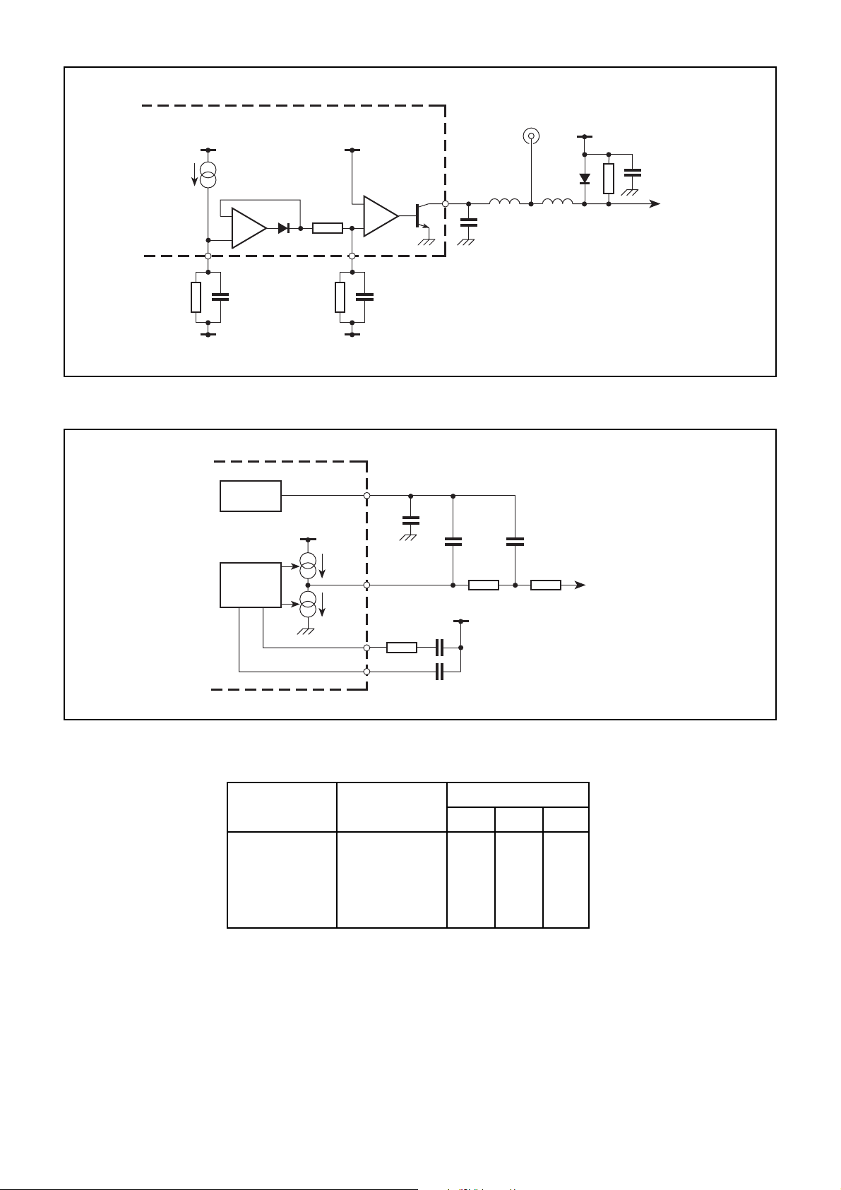
Audio AGC (Fig. 3)
The Audio AGC consists of a current sink which is controlled by the audio (baseband) signal. It has three parameters
that may be controlled by the user. These are the attack (turn
on ) time, decay (duration) time and threshold level. The
attack time is simply determined by the value of the external
capacitor connected to TCADJ. The external capacitor is in
series with an internal 100kΩ resistor and the time constant
of this circuit dictates the attack time of the AGC.
i.e. t
The decay time is determined by the external resistor
connected in parallel with the capacitor CTC. The decay time
is simply
When a large audio (baseband) signal is incident on the
input to the AGC circuit, the variable current source is turned
on. This causes a voltage drop across R13. The voltage
potential between V
current to flow in pin 30. This charges up C18 through the
100kΩ internal resistor. As the voltage across the capacitor
increases, a current source is turned on and this sinks current
from pin 32. The current sink on pin 32 can be used to drive
= 100kΩ3C18
ATTACK
t
= R173C18
DECAY
and the voltage on pin 31 causes a
REF
SL6619
the external AGC circuit by causing a PIN diode to conduct,
reducing the signal to the RF amplifier.
RF AGC
The RF AGC is an automatic gain control loop that
protects the mixer’s RF inputs, Pins 3 and 5, from large out of
band RF signals. The loop consists of an RF received signal
strength indicator which detect the signal at the inputs of the
mixers. This RSSI signal is then used to control the LNA
current source (pin 1).
Regulator
The on-chip regulator should be used in conjunction with
a suitable PNP transistor to achieve regulation. As the transistor forms part of the regulator feedback loop the transistor
should exhibit the following characteristics:
H
.100 for VCE. = 0·1V
FE
If no external transistor is used, the maximum current
sourcing capability of the regulator is limited to 30µA.
Automatic Frequency Control (Fig. 4)
The Automatic Frequency Control consists of a detection
circuit which gives a current output at AFC OP whose magnitude and sign is a function of the difference between the local
oscillator (f
is then filtered by an off-chip integrating capacitor. The
integrator’s output voltage is used to control a voltage control
crystal oscillator. This closes the AFC feedback loop giving
the automatic frequency control function. For an FSK modulated incoming RF carrier, the AFC OP current’s polarity is
positive, i.e.current is sourced for f
negative, i.e. current is sunk, for fLO.fC.fLO24kHz. The
magnitude of the AFC OP current is a function of frequency
offset and the transmitted data’s bit stream. If the carrier
frequency, (f
then the magnitude of the current is zero.
BIT RATE FILTER CONTROL
The logic level on pin 26 controls the cutoff frequency of
the 1st order bit rate for a given bit rate filter capacitor at pin
27. This allows the cutoff frequency to be changed between
f
, 2fC and 0·43fC through the logic level on pin 26. This
C
function is achieved by changing the value of the current in the
4f detector’s output stage. A logic zero (0V to 0·1V) on pin 26
gives a cutoff frequency of f
gives a cut off frequency of 2fC and an open circuit at pin 26
gives a cutoff frequency of 0·43f
) and carrier frequencies (fC). This output current
LO
LO,fC,fLO
), equals the local oscillator frequency, (fLO)
C
a logic one (VCC220·3V to VCC2)
C
.
C
14kHz and
9
Page 10
SL6619
CURRENT
SOURCE 1
R13 C34
SL6619
V
CC
−
+
32 31
V
REF
R
DECAY
100k
R17
V
REF
SL6619
VOLTAGE
REFERENCE
VCC2
VCC2
AFC
DETECTION
CIRCUIT
0µA/5µA
5µA/0µA
15mV
−
+
C18
C
TC
V
REF
Fig.3 AGC schematic
18
C
VREF
19
R11
24
C21
30
C15
C
1
INT
R15 320k
VCC1
RF
INPUT
C30
C
INT
VCC1
TO RF AMP
2
TO VCXO
VARACTOR
DIODE
Peak deviation
(kHz)
3·5
4
4·5
5
5·5
25
C22
Fig. 4 AFC schematic
Baud rate
(bps)
512, 1200, 2400
512, 1200, 2400
512, 1200, 2400
512, 1200, 2400
512, 1200, 2400
Component (Fig. 4)
C22 C21 R11
750pF
560pF
510pF
470pF
430pF
2·0nF
1·5nF
1·3nF
1·2nF
1·1nF
Table 2 AFC defining components
15kΩ
15kΩ
15kΩ
15kΩ
15kΩ
10
Page 11
SL6619
1
CC
V
1
CC
V
BRF CNT
TP LIM I
REF
V
C23 C24
C21
C22
C27
C18
R17
R13
C34
2
CC
V
2
CC
V
R16
R11
AFC1
BATT FLAG
24
IRF
23
1
2
GND
TO TR2
R10
1
CC
V
1
CC
V
AFC2
BRF CNT
BRF1
VBATT
TP LIM I
IAGC OP
TC ADJ
GTH ADJ
32 31 30 29 28 27 26 25
C20
C19
2
CC
V
MIXIP A
R9
22
3
DATA OP
R8
DATA OP
21
SL6619
4
MIX DEC
C25
T1
BEC
BEC
20
5
MIXIP B
AFC OP
R15
C15 C30
AFC OP
19
6
REG CNT
C26
TR3
REF
V
REG
V
REF
V
18
7
C16 C17
TPQ
TPI
17
8
REG
V
1
CC
V
9 10111213141516
1
CC
V
R7
C12
R5
C14
LO
EXT
C11R4
1
CC
V
C13
R6
C32C29
Q2
Q1
LOIP Q
R14
GYR I
LOIP I
CC
1
V
I2
C9 C10
I1
IRF
FROM
REF
V
VC1
R3
TR1
R2
C6 C33
C6 C33
1
CC
V
C7
C8
(PIN 1)
TR2
C3
L1
C2C1
R1
C5
C4
REG
V
REG
V
C28
R12
RF IN
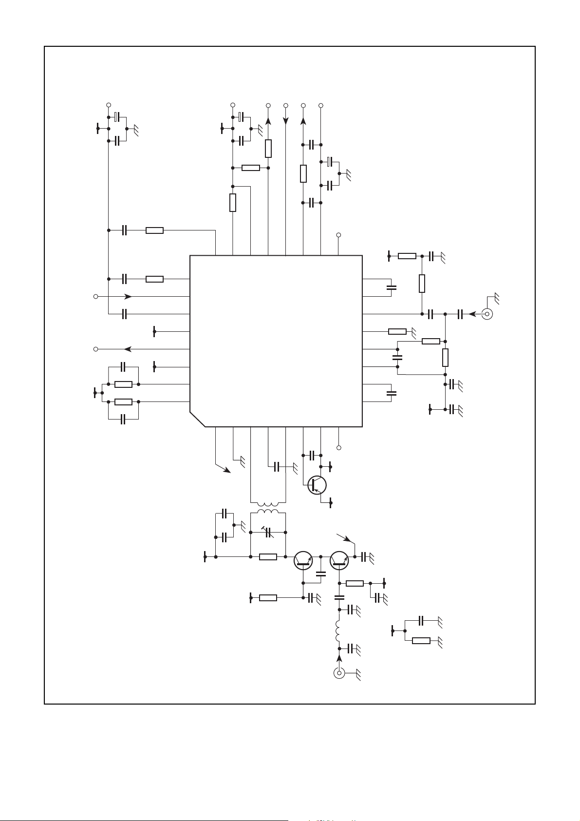
Fig. 5 SL6619 characterisation circuit (see Tables 3 and 4 for component values)
11
Page 12
SL6619
Resistors Capacitors Capacitors (cont.) Inductors
R1 4·7kΩ
R2 4·7kΩ
R3 2kΩ
R4 100Ω
R5 100Ω
R6 100Ω
R7 100Ω
R8 430kΩ
R9 220kΩ
R10 S/C
R11 15kΩ
R12 2kΩ
R13 33kΩ
R14 180kΩ
R15 430kΩ
R16 220kΩ
R17 220kΩ
Resistors
R1 4·7kΩ
R2 4·7kΩ
R3 1·8kΩ
R4 100Ω
R5 100Ω
R6 100Ω
R7 100Ω
R8 430kΩ
R9 220kΩ
R10 S/C
R11 15kΩ
R12 2kΩ
R13 33kΩ
R14 180kΩ
R15 430kΩ
R16 220kΩ
R17 220kΩ
C1 12pF
C2 O/C
C3 220nF
C4 1nF
C5 1nF
C6 1nF
C7 1nF
C8 3·3pF
C9 4·7nF
C10 4·7nF
C11 4·7pF
C12 5·6pF
C13 1nF
C14 1nF
C15 1nF
C16 1nF
C17 2·2µF
C18 100nF
C19 1nF
C20 2·2µF
C21 1·5nF
C22 560pF
C23 1nF
C24 2·2µF
C25 100nF
C26 100nF
C27 560pF
C28 1nF
C29 1nF
C30 1nF
C32 100nF
C33 100nF
C34 100nF
VC1 3-10pF
L1 56nH
T1 30nH 1:1, Coilcraft M1686-A
Transistors
TR1 Toshiba 2SC5065
TR2 Toshiba 2SC5065
TR3 FMMT589 (Zetex ZTX550)
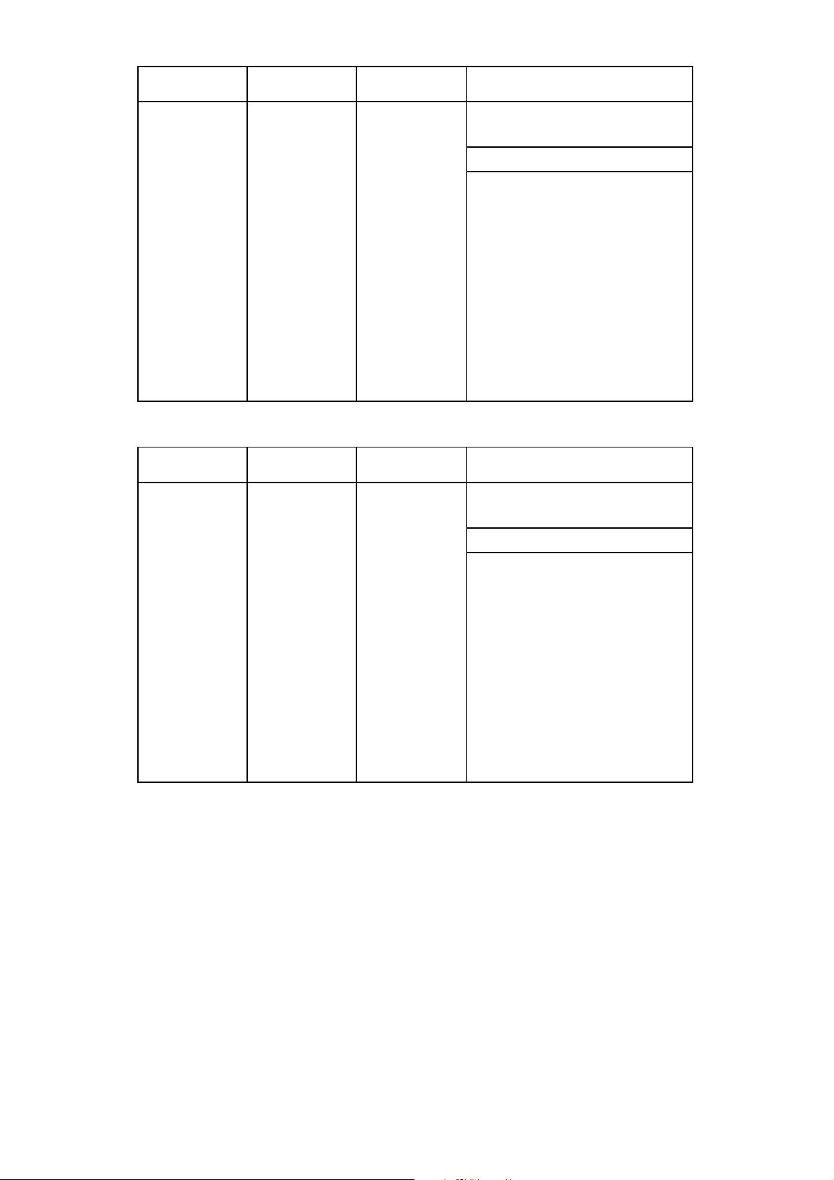
Table 3 Component list for 280MHz characterisation board
Capacitors Capacitors (cont.) Inductors
C1 O/C
C2 O/C
C3 1nF
C4 1nF
C5 1nF
C6 1nF
C7 1nF
C8 3·3pF
C9 4·7nF
C10 4·7nF
C11 3·9pF
C12 3·3pF
C13 1nF
C14 1nF
C15 1nF
C16 1nF
C17 2·2µF
C18 100nF
C19 1nF
C20 2·2µF
C21 1·5nF
C22 560pF
C23 1nF
C24 2·2µF
C25 100nF
C26 100nF
C27 560pF
C28 1nF
C29 1nF
C30 1nF
C32 100nF
C33 100nF
C34 100nF
VC1 3-10pF
L1 47nH
T1 16nH 1:1, Coilcraft Q4123-A
Transistors
TR1 Philips BFT25A
TR2 Philips BFT25A
TR3 FMMT589 (Zetex ZTX550)
12
Table 4 Component list for 450MHz characterisation board
Page 13
TYPICAL DC PARAMETERS (FIGS. 6 TO 8)
SL6619
2·00
1·80
1·60
1·40
1·20
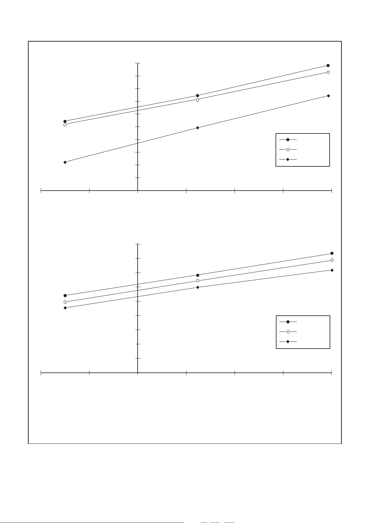
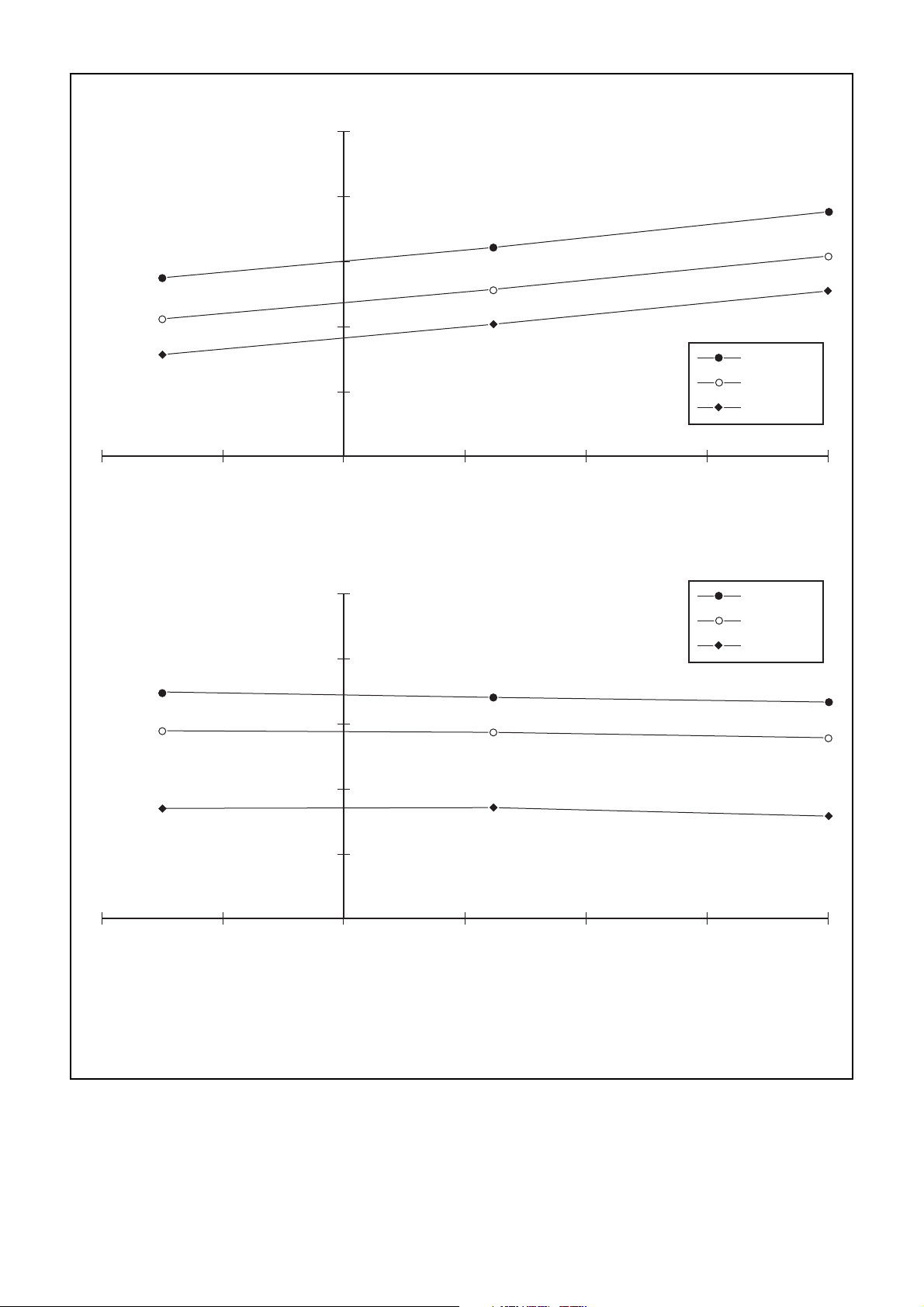
Fig. 6a Typical I
CC
1
1 (mA)
CC
I
240 220 0 20 40 60 80
1·00
0·80
0·60
0·40
0·20
VCC = 3·0, 4·0
V
CC
= 1·3, 2·7
V
CC
= 1·0, 1·9
TEMPERATURE °C
0·45
Fig. 6b Typical ICC2
0·40
0·35
0·30
2 (mA)
CC
I
240 220 0 20 40 60 80
0·25
0·20
0·15
0·10
0·05
VCC = 3·0, 4·0
CC
= 1·3, 2·7
V
CC
= 1·0, 1·9
V
TEMPERATURE °C
Conditions
Standard Mitel characterisation board (Fig. 5)
I
1 includes IRF LNA current (typ. 500µA) but does not include the regulator load current
CC
The Audio AGC and RF AGC are both inactive
I
2 is measured with BATTFLAG and DATAS OP high, fC = 282MHz
CC
V
connected to VCC1
BATT
Fig. 6 Typical ICC1 and ICC2 v. supply and temperature
13
Page 14
SL6619
1·30
1·28
(V)
REF
V
240 220 0 20 40 60 80
1·26
1·24
1·22
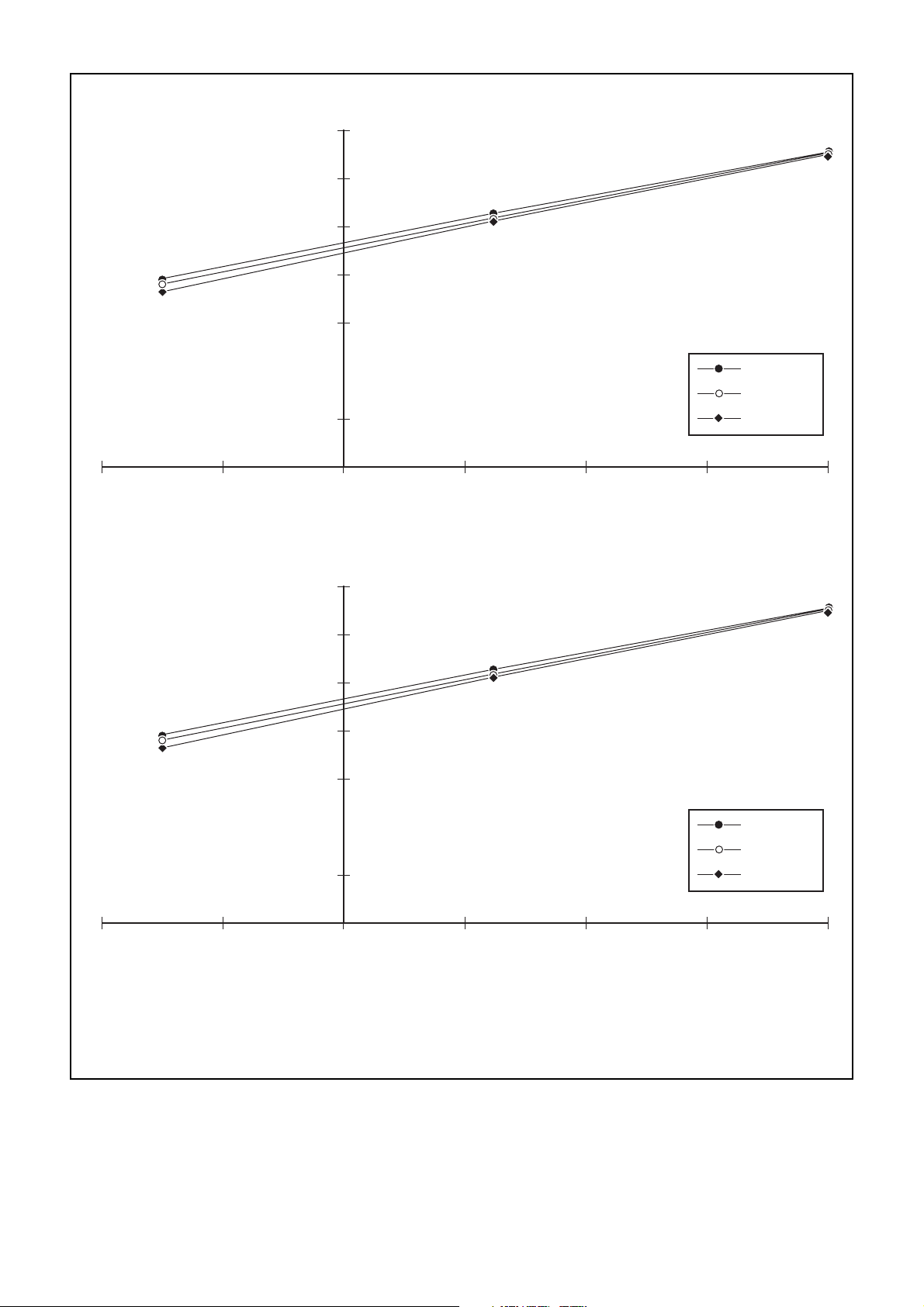
Fig. 7a Typical V
REF
VCC = 3·0, 4·0
V
CC
= 1·3, 2·7
V
CC
= 1·0, 1·9
TEMPERATURE °C
1·05
1·03
(V)
REG
V
240 220 0 20 40 60 80
1·01
0·99
0·97
Fig. 7b Typical V
(load = 2·2kΩ to GND)
REG
VCC = 3·0, 4·0
V
CC
= 1·3, 2·7
V
CC
= 1·0, 1·9
TEMPERATURE °C
Conditions
Standard Mitel characterisation board (Fig. 5)
I
1 includes IRF LNA current (typ. 500µA) but does not include the regulator load current
CC
The Audio AGC and RF AGC are both inactive
I
2 is measured with BATTFLAG and DATAS OP high, fC = 282MHz
CC
V
connected to VCC1
BATT
14
Fig. 7 Typical V
REF
and V
v. supply and temperature
REG
Page 15
SL6619
700
600
500
(µA)
RF
I
240 220 0 20 40 60 80
400
300
200
100
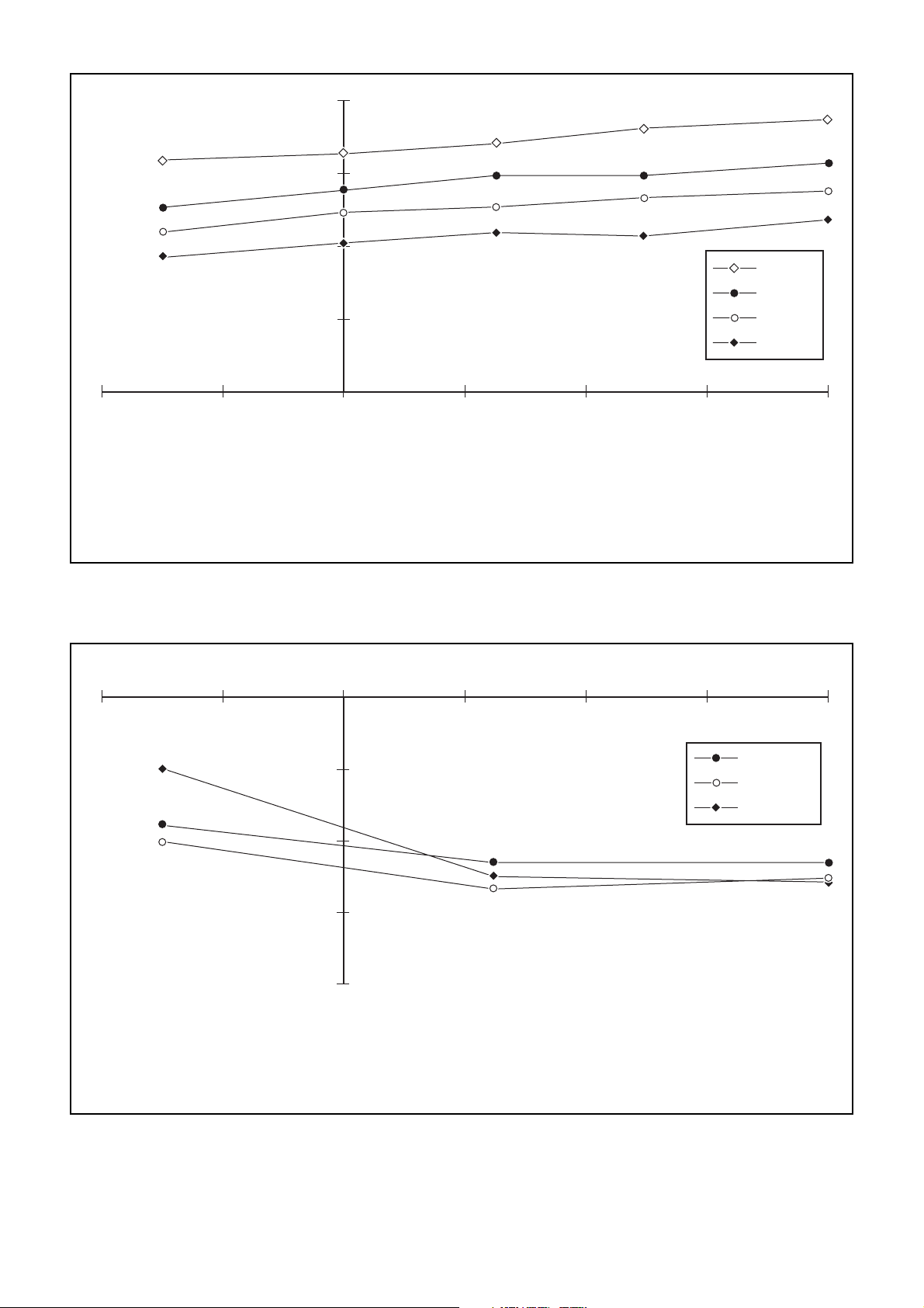
Fig. 8a Typical IRF (V
IRF
= 0·3V)
VCC = 3·0, 4·0
V
CC
= 1·3, 2·7
CC
= 1·0, 1·9
V
TEMPERATURE °C
700
600
500
(µA)
RF
I
240 220 0 20 40 60 80
400
300
200
100
Fig. 8b Typical IRF (V
IRF
= 1·3V)
VCC = 3·0, 4·0
V
CC
= 1·3, 2·7
CC
= 1·0, 1·9
V
TEMPERATURE °C
Conditions
Standard Mitel characterisation board (Fig. 5)
I
1 includes IRF LNA current (typ. 500µA) but does not include the regulator load current
CC
The Audio AGC and RF AGC are both inactive
I
2 is measured with BATTFLAG and DATAS OP high, fC = 282MHz
CC
V
connected to VCC1
BATT
Fig. 8 Typical IRF v. supply and temperature
15
Page 16
SL6619
TRIGGER VOLTAGE (V)
V
BATT
1·1
1·08
1·06
1·04
VCC = 3·5
VCC = 2·7
CC = 2·3
V
CC = 1·9
V
240
220 0 20 40 60 80
TEMPERATURE °C
Conditions
Standard Mitel characterisation board (Fig. 5)
I
1 includes IRF LNA current (typ. 500µA) but does not include the regulator load current
CC
The Audio AGC and RF AGC are both inactive
I
2 is measured with BATTFLAG and DATAS OP high, fC = 282MHz
CC
V
connected to VCC1
BATT
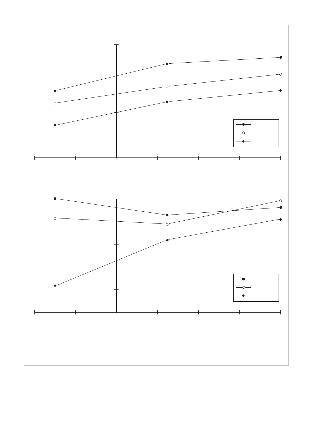
Fig. 9 Typical battery flag trigger voltage (V
BATTFLAG
= VCC/2) v. supply and temperature
TYPICAL AC PARAMETERS (FIGS. 10 TO 13)
240 220 0 20 40 60 80
2124·00
2126·00
TEMPERATURE °C
VCC = 3·0, 4·0
CC = 1·3, 2·7
V
CC = 1·0, 1·9
V
2128·00
SENSITIVITY (1 IN 30 BER) (dBm)
2130·00
Conditions
282 Mitel characterisation board (Fig. 5), f
= 282MHz
C
1200bps baud rate, 4kHz peak deviation frequency, BER 1 in 30
The LNA gain is set such that an RF signal of 273dBm at the LNA input, offset from the LO by 4kHz, gives a typical signal
level of 300mVp-p at TPI and TPQ
Fig. 10 Typical sensitivity v. supply and temperature
16
Page 17
SL6619
60
58
56
Fig. 11a Typical IP3
IP3(dB)
54
VCC = 3·0, 4·0
V
CC
CC
V
= 1·3, 2·7
= 1·0, 1·9
52
240 220 0 20 40 60 80
TEMPERATURE °C
75
74
73
ADJACENT CHANNEL (dB)
240 220 0 20 40 60 80
72
71
Fig. 11b Typical adjacent channel
VCC = 3·0, 4·0
V
CC
= 1·3, 2·7
CC
= 1·0, 1·9
V
TEMPERATURE °C
Conditions
282 Mitel characterisation board (Fig. 5), fC = 282MHz
1200bps baud rate, 4kHz peak deviation frequency, BER 1 in 30
The LNA gain is set such that an RF signal of 273dBm at the LNA input, offset from the LO by 4kHz, gives a typical signal
level of 300mVp-p at TPI and TPQ
Fig. 11 Typical IP3 and adjacent channel v. supply and temperature
17
Page 18
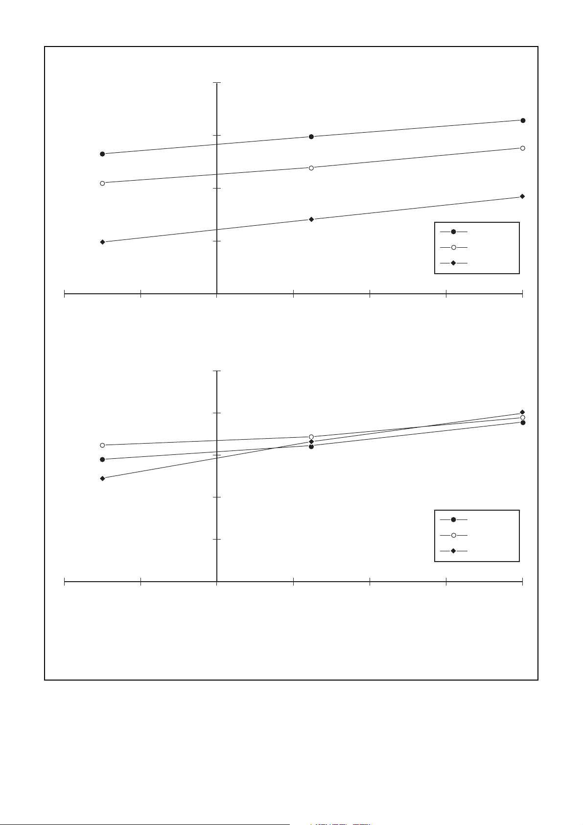
SL6619
4·0
3·5
3·0
DEVIATION ACCEPTANCE UP (kHz)
240 220 0 20 40 60 80
2·5
Fig. 12a Typial deviation acceptance UP
VCC = 3·0, 4·0
V
CC
= 1·3, 2·7
CC
= 1·0, 1·9
V
TEMPERATURE °C
2·5
2·4
2·3
2·2
2·1
DEVIATION ACCEPTANCE DOWN (kHz)
240 220 0 20 40 60 80
Fig 12b Typical deviation acceptance DOWN
VCC = 3·0, 4·0
V
CC
= 1·3, 2·7
CC
= 1·0, 1·9
V
TEMPERATURE °C
Conditions
282 Mitel characterisation board (Fig. 5), fC = 282MHz
1200bps baud rate, 4kHz peak deviation frequency, BER 1 in 30
The LNA gain is set such that an RF signal of 273dBm at the LNA input, offset from the LO by 4kHz, gives a typical signal
level of 300mVp-p at TPI and TPQ
18
Fig. 12 Typical deviation acceptance v. supply and temperature
Page 19
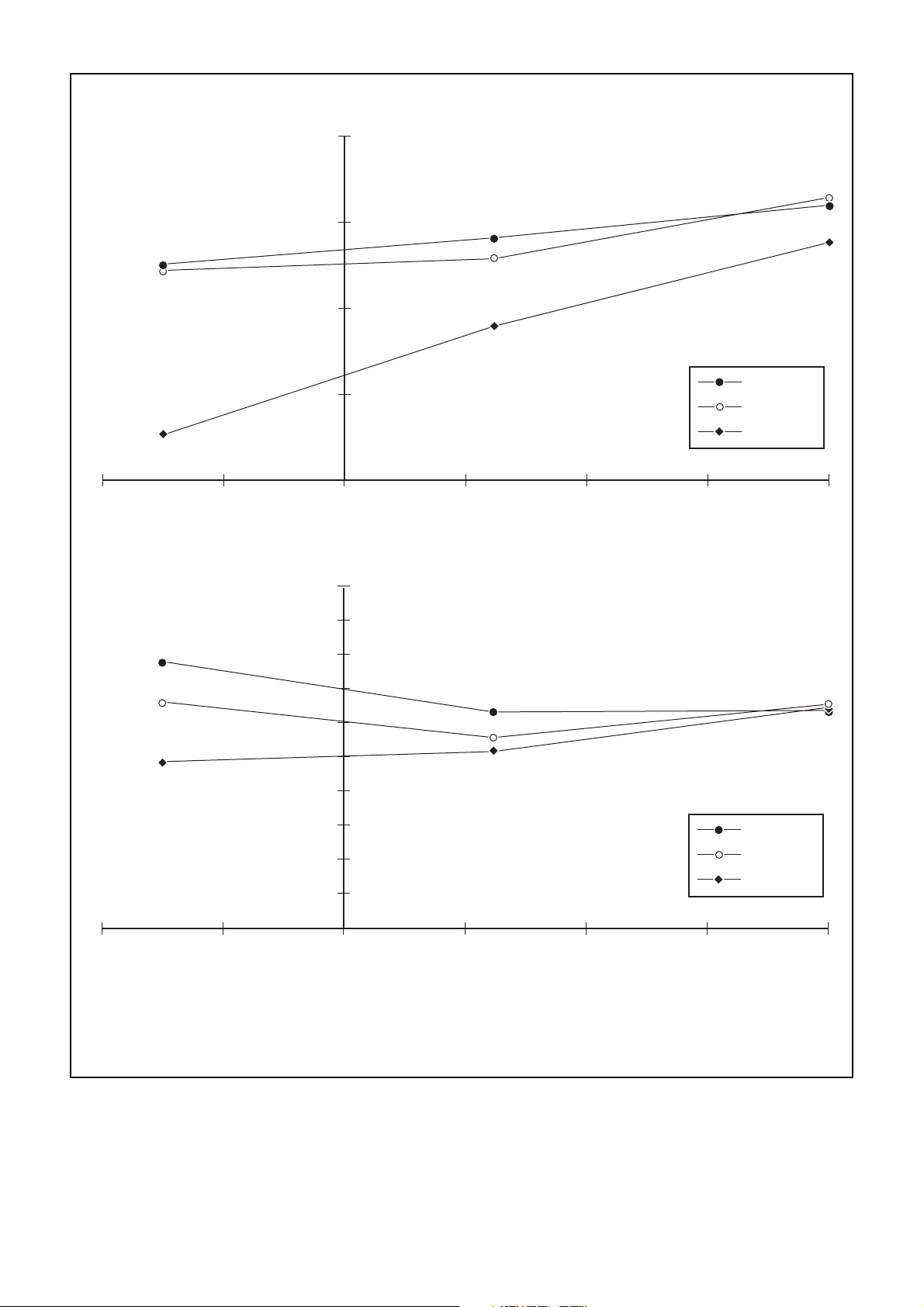
SL6619
2·7
2·6
2·5
2·4
CENTRE FREQUENCY ACCEPTANCE (kHz)
240 220 0 20 40 60 80
Fig. 13a Typical centre frequency acceptance
VCC = 3·0, 4·0
CC
= 1·3, 2·7
V
CC
= 1·0, 1·9
V
TEMPERATURE °C
80
Fig. 13b Typical1MHz blocking
79
78
77
76
1MHz BLOCKING ( dB)
75
74
73
72
71
240 220 0 20 40 60 80
VCC = 3·0, 4·0
V
CC
= 1·3, 2·7
CC
= 1·0, 1·9
V
TEMPERATURE °C
Conditions
282 Mitel characterisation board (Fig. 5), fC = 282MHz
1200bps baud rate, 4kHz peak deviation frequency, BER 1 in 30
The LNA gain is set such that an RF signal of 273dBm at the LNA input, offset from the LO by 4kHz, gives a typical signal
level of 300mVp-p at TPI and TPQ
Fig. 13 Typical centre frequency acceptance and 1MHz blocking v. supply and temperature
19
Page 20
Page 21

http://www.mitelsemi.com
World Headquarters - Canada
Tel: +1 (613) 592 2122
Fax: +1 (613) 592 6909
North America Asia/Pacific Europe, Middle East,
Tel: +1 (770) 486 0194 Tel: +65 333 6193 and Africa (EMEA)
Fax: +1 (770) 631 8213 Fax: +65 333 6192 Tel: +44 (0) 1793 518528
Fax: +44 (0) 1793 518581
Information relating to products and services furnished herein by Mitel Corporation or its subsidiaries (collectively “Mitel”) is believed to be reliable. However, Mitel assumes no
liability for errors that may appear in this publication, or for liability otherwise arising from the application or use of any such information, product or service or for any infringement of
patents or other intellectual property rights owned by third parties which may result from such application or use. Neither the supply of such information or purchase of product or
service conveys any license, either express or implied, under patents or other intellectual property rights owned by Mitel or licensed from third parties by Mitel, whatsoever.
Purchasers of products are also hereby notified that the use of product in certain ways or in combination with Mitel, or non-Mitel furnished goods or services may infringe patents or
other intellectual property rights owned by Mitel.
This publication is issued to provide information only and (unless agreed by Mitel in writing) may not be used, applied or reproduced for any purpose nor form par t of any order or
contract nor to be regarded as a representation relating to the products or services concerned. The products, their specifications, services and other information appearing in this
publication are subject to change by Mitel without notice. No warranty or guarantee express or implied is made regarding the capability, performance or suitability of any product or
service. Information concerning possible methods of use is provided as a guide only and does not constitute any guarantee that such methods of use will be satisfactory in a specific
piece of equipment. It is the user’s responsibility to fully determine the performance and suitability of any equipment using such information and to ensure that any publication or
data used is up to date and has not been superseded. Manufacturing does not necessarily include testing of all functions or parameters. These products are not suitable for use in
any medical products whose failure to perform may result in significant injury or death to the user. All products and materials are sold and services provided subject to Mitel’s
conditions of sale which are available on request.
M Mitel (design) and ST-BUS are registered trademarks of MITEL Corporation
Mitel Semiconductor is an ISO 9001 Registered Company
Copyright 1999 MITEL Corporation
All Rights Reserved
Printed in CANADA
TECHNICAL DOCUMENTATION - NOT FOR RESALE
 Loading...