

Page 1

THIS DOCUMENT IS FOR MAINTENANCE
PURPOSES ONLY AND IS NOT
RECOMMENDED FOR NEW DESIGNS
Page 2
SL560
300MHz LOW NOISE AMPLIFIER
This monolithic circuit contains three very high performance
transistors and associated biasing components in an eightlead TO-5 package forming a 300MHz low noise amplifier. The
configuration employed permits maximum flexibility with
minimum use of external components. The SL560C is a
general purpose low noise, high frequency gain block.
The device is also available as the SL560AC which has
guaranteed operation over the fully Military Temperatures
Range and is screened to MIL-STD-883 Class B. Data is
available separately.
FEATURES
■ Gain up to 40dB
■ Noise Figures less than 2dB (Rs 200 ohm)
■ Bandwidth 300MHz
■ Supply Voltage 2-15V (Depending on Configuration)
■ Low Power Consumption
APPLICATIONS
■ Radar IF Preamplifiers
■ Infra-Red Sysems Head Amplifiers
■ Amplifiers in Noise Measurement Systems
■ Low Power Wideband Amplifiers
■ Instrumentation Preamplifiers
■ 50 ohm Line Drivers
■ Wideband Power Amplifiers
■ Wideband Dynamic Range IF Amplifiers
■ Aerial Preamplifiers
ABSOLUTE MAXIMUM RATINGS
Supply voltage +15V
Storage temperature
SL560C DP -55°C to +150°C
SL560C CM -65°C to +150°C
Junction temperature
SL560C DP +150°C
SL560C CM +175°C
Operating temperature range
SL560C DP -30°C to +85°C
SL560C CM -55°C to +125°C
Thermal resistance
Chip-to-ambient
SL560C CM 225°C/W
SL560C DP 111°C/W
Chip-to-case
SL560C CM 65°C/W
SL560C DP 71°C/W
ADVANCE INFORMATION
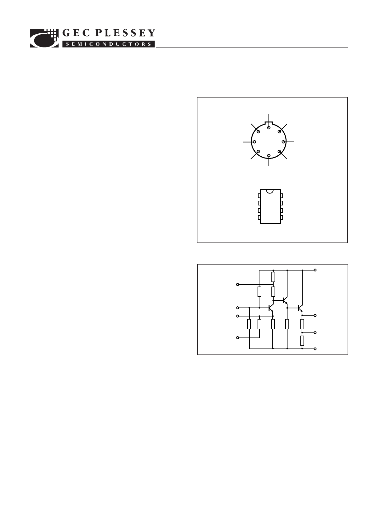
INPUT
GAIN SET
50 APPLICATIONS
8
71
6
SL560
53
4
Vcc
INPUT
COMMON BASE
CONFIGURATION
INPUT
COMMON EMITTER
CONFIGURATION
Bottom view
Vcc
1
2
SL
560
3
4
GROUND
OUTPUT CURRENT SET
OUTPUT
Top view
Fig.1 Pin connections
GAIN SET 5
10k
INPUT
(COMMON EMITTER
CONFIGURATION)
INPUT
(COMMON BASE
CONFIGURATION)
INPUT
(50 APPLICATIONS)
6
7
8
Fig.2 SL560C circuit diagram
ORDERING INFORMATION
SL560 C CM
SL560 C DP
5962-90520 (SMD)
DS3297 - 2.1
GROUND
2
OUTPUT CURRENT SET
OUTPUT
8
INPUT 50 OHMS APPLICATIONS
7
INPUT COMMON BASE
6
INPUT COMMON EMITTER
GAIN SET
5
4 Vcc
560
240
TR1
TR3TR2
3 OUTPUT
5003010k 1k 200
2
2k
1 GROUND
SL560
CM8
DP8
OUTPUT CURRENT
SET
Page 3
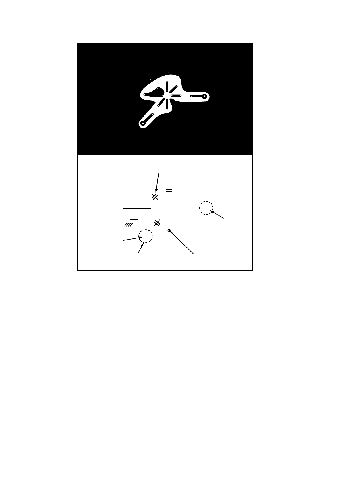
SL560
SUPPLY DECOUPLING
CAPACITOR
+V
CC
GROUND
O/P
6
75
4
SUBVIS/BNC
8
13
2
LINK
SOCKET
Fig.3 PC layout for 50Ω line driver (see Fig.6)
I/P
Page 4

ELECTRICAL CHARACTERISTICS
These characteristics are guaranteed over the following conditions (unless otherwise stated)
Frequency = 30MHz; V
=6V; RS = RL =50Ω; T
CC
=22°C ± 2°C; Test Circuit: Fig.6
AMB
SL560
Characteristic
Small signal voltage gain
Gain flatness
Upper cut-off frequency
Output swing
Typ.Min. Max. Units
11
14
±1.5
250
+5
+7
+11
Noise figure (common emitter)
1.8
3.5
Supply current
20
CIRCUIT DESCRIPTION
Three high performance transistors of identical geometry
are employed. Advanced design and processing techniques
enable these devices to combine a low base resistance (Rbb')
of 17Ω (for low noise operation) with a small physical size giving a transition frequency, f
The input transistor (TR1) is normally operating in common
base, giving a well defined low input impedance. The full
voltage gain is produced by this transistor and the output
voltage produced at its collector buffered by the two emitter
followers (TR2 and TR3). To obtain maximum bandwidth the
capacitance at the collector of TR1 must be minimised. Hence,
to avoid bonding pad and can capacitances, this point is not
brought out of the package. The collector load resistance of
TR1 is split, the tapping being accessible via pin 5. If required,
an external roll-off capacitor can be fixed to this point.
, in excess of 1GHz.
T
Conditions
17
dB
dB
10MHz - 220MHz
MHz
6V
V
CC
V
= 9V
CC
RS = 200Ω
R
= 50Ω
S
30
dBm
dBm
dB
dB
mA
The large number of circuit nodes accessible from the
outside of the packages affords great flexibility, enabling the
operating current and circuit configuration to be optimised for
any application. In particular, the input transistor (TR1) can be
operated in common emitter mode by decoupling pin 7 and
using 6 as the input. In this configuration, a 2dB noise figure
(R
= 200Ω) can be achieved. This configuration can give a
S
gain of 35dB with a bandwidth of 300MHz (see figs. 10 and 11).
Because the transistors used in the SL560C exhibit a high
value of f
instability. Capacitors of small physical size should be used,
, care must be taken to avoid high frequency
T
the leads of which must be short as possible to avoid oscillation
brought about by stray inductance. The use of a ground plane
is recommended.
15
10
GAIN (dB)
5
0
10 30 50 100 200 300
TA = +25°C
VCC = 6V
P
= (a) +5dBm
OUT
(b) 0dBm
FREQUENCY (MHz)
Fig.4 Frequency response, small signal gain is of a
typical device
12
10
(b)
(a)
8
6
POUT (dBm)
4
2
0
10 30 100 200 300
TA = +25°C
VCC = a) 6V
(b) 9V
FREQUENCY (MHz)
(b)
(a)
Fig.5. Frequency response, output capability (loci of maximum
output power with frequency for 1dB gain compression (typical)
Page 5

SL560
TYPICAL APPLICATIONS
50
OUTPUT
10n
4
35
26
17
8
10n
10n
+6V
1.8
1.6
1.4
TA = +25°C
VCC = (a) 3V
(b) 6V
(c) 9V
(a)
INPUT
10n
Gain 14dB
Bandwidth 220MHz (P
200MHz (P
= 1mW, 50Ω)
OUT
= 5mW, 50Ω)
OUT
Input SWR 1.5:1
Fig.6 50Ω lin driver. The response of this configuration is
shown in Fig.4
V
CC
10n
INPUT
10k
10n
0V
OUTPUT
10n
4
35
26
17
8
Voltage gain 32dB at 6V
35dB at 10V
Noise figure 1.8dB (Rs = 200Ω)
Supply current 6mA at 6V
12mA at 10V
Bandwidth 75MHz (see Fig.9)
INPUT VSWR
1.2
10 100 200 400
FREQUENCY (MHz)
(b)
(c)
300
Fig.7 Input standing wave ratio plot of circuit shown
in Fig.6 (typical)
40
35
30
25
20
15
GAIN (dB)
10
5
0
10 20 30 50 100 200300 500 1000
FREQUENCY (MHz)
Fig.8 Low Noise preamplifier Fig.9 Frequency response of circuit shown in Fig.8 (typical)
1n
470
OUTPUT
1n
26
4
35
17
8
27p
Gain 13dB at Vcc = 9V
-1dB at 6MHz and 300MHz
Fig.10 Wide bandwidth amplifier
VCC
10n
INPUT
1n
15
56p
15
0V
15
10
GAIN (dB)
5
(b)
(a)
TA = +25°C
VCC = (a) 6V
(b) 9V
10 100 200300400
FREQUENCY (MHz)
Fig.11 Frequency response of circuit shown in Fig.10 (typical)
Page 6

SL560
OUTPUT
1n
35
26
17
4
8
Fig.12 Three-stage directly-coupled high gain low noise amplifier
60
40
GAIN (dB)
20
0 20 50 70 100 200 300
TA = +25°C
VCC = (a) 4V
(b) 6V
(c) 9V
FREQUENCY (MHz)
4
8
10n
0.1
47µ
µ
INPUT
1n1n1n
4
35
26
17
8
10n
+2V
10n
INPUT
0V
0.1µ
4
35
26
17
8
(c)
(b)
(a)
35
26
17
OUTPUT
Gain 13dB
Power supply current 3mA
Bandwidth 125MHz
Noise figure 2.5dB (Rs = 200Ω)
Fig.13 Frequency response of circuit shown in Fig.12
(typical)
700
600
500
400
300
200
DISSIPATION (mW)
100
40 50 60 70 80 90 100 110 120 130 140 150
Fig.15 Ambient operating temperature V. degrees centigrade
Fig.14 Low power consumption amplifier
TO5
DIP
TEMPERATURE (°C)
(typical)
Page 7

SL560
HEADQUARTERS OPERATIONS
GEC PLESSEY SEMICONDUCTORS
Cheney Manor, Swindon,
Wiltshire SN2 2QW, United Kingdom.
Tel: (0793) 518000
Fax: (0793) 518411
CUSTOMER SERVICE CENTRES
• FRANCE & BENELUX Les Ulis Cedex Tel: (1) 64 46 23 45 Fax : (1) 64 46 06 07
• GERMANY Munich Tel: (089) 3609 06-0 Fax : (089) 3609 06-55
• ITALY Milan Tel: (02) 66040867 Fax: (02) 66040993
• JAPAN Tokyo Tel: (03) 5276-5501 Fax: (03) 5276-5510
• NORTH AMERICA Scotts Valley, USA Tel (408) 438 2900 Fax: (408) 438 7023.
• SOUTH EAST ASIA Singapore Tel: (65) 3827708 Fax: (65) 3828872
GEC PLESSEY SEMICONDUCTORS
P.O. Box 660017
1500 Green Hills Road,
• SWEDEN Stockholm, Tel: 46 8 702 97 70 Fax: 46 8 640 47 36
• UK, EIRE, DENMARK, FINLAND & NORWAY
Swindon Tel: (0793) 518510 Fax : (0793) 518582
Scotts Valley, California 95067-0017,
United States of America.
These are supported by Agents and Distributors in major countries world-wide.
Tel: (408) 438 2900
Fax: (408) 438 5576
This publication is issued to provide information only which (unless agreed by the Company in writing) may not be used, applied or reproduced for any purpose nor form part of any order or contract nor to be regarded
as a representation relating to the products or services concerned. No warranty or guarantee express or implied is made regarding the capability, performance or suitability of any product or service. The Company
reserves the right to alter without prior knowledge the specification, design or price of any product or service. Information concerning possible methods of use is provided as a guide only and does not constitute
any guarantee that such methods of use will be satisfactory in a specific piece of equipment. It is the user's responsibility to fully determine the performance and suitability of any equipment using such information
and to ensure that any publication or data used is up to date and has not been superseded. These products are not suitable for use in any medical products whose failure to perform may result in significant injury
or death to the user. All products and materials are sold and services provided subject to the Company's conditions of sale, which are available on request.
GEC Plessey Semiconductors 1994
Page 8

For more information about all Zarlink products
visit our Web Site at
www.zarlink.com
Information relating to products and services furnished herein by Zarlink Semiconductor Inc. trading as Zarlink Semiconductor or its subsidiaries (collectively
is believed to be reliable. However, Zarlink assumes no liability for errors that may appear in this publication, or for liability otherwise arising from the application or
use of any such information, product or service or for any infringement of patents or other intellectual property rights owned by third parties which may result from
such application or use. Neither the supply of such information or purchase of product or service conveys any license, either express or implied, under patents or
other intellectual property rights owned by Zarlink or licensed from third parties by Zarlink, whatsoever. Purchasers of products are also hereby notified that the use
of product in certain ways or in combination with Zarlink, or non-Zarlink furnished goods or services may infringe patents or other intellectual property rights owned
by Zarlink.
This publication is issued to provide information only and (unless agreed by Zarlink in writing) may not be used, applied or reproduced for any purpose nor form part
of any order or contract nor to be regarded as a representation relating to the products or services concerned. The products, their specifications, services and other
information appearing in this publication are subject to change by Zarlink without notice. No warranty or guarantee express or implied is made regarding the capability,
performance or suitability of any product or service. Information concerning possible methods of use is provided as a guide only and does not constitute any guarantee
that such methods of use will be satisfactory in a specific piece of equipment. It is the user
equipment using such information and to ensure that any publication or data used is up to date and has not been superseded. Manufacturing does not necessarily
include testing of all functions or parameters. These products are not suitable for use in any medical products whose failure to perform may result in significant injury
or death to the user. All products and materials are sold and services provided subject to Zarlink
Purchase of Zarlink s I
that the system conforms to the I
2
C components conveys a licence under the Philips I
2
C Standard Specification as defined by Philips.
’
s responsibility to fully determine the performance and suitability of any
’
s conditions of sale which are available on request.
2
C Patent rights to use these components in and I
2
C System, provided
“
Zarlink
Zarlink and the Zarlink Semiconductor logo are trademarks of Zarlink Semiconductor Inc.
Copyright 2001, Zarlink Semiconductor Inc. All Rights Reserved.
”
)
TECHNICAL DOCUMENTATION - NOT FOR RESALE
 Loading...