

Page 1
Color Television Chassis
21SL7
SK7.0L
CA
21SL7
Contents Page
1. Revision List 2
2. Technical Specifications and Connections 2
3. Precautions, Notes, and Abbreviation List 3
4. Mechanical Instructions 7
5. Service Modes, Error Codes, and Fault Finding 8
6. Alignments 9
7. Circuit Descriptions 21
8. IC Data Sheets 22
9. Block Diagrams
PWB locations 27
Block Diagram Chassis 28
10. Circuit Diagrams and PWB Layouts Diagram PWB
21SL7 Schematic Overview Chassis
CRT panel (B) 32 32
(A) 29 30-31
©
Copyright 2010 Koninklijke Philips Electronics N.V.
All rights reserved. No part of this publication may be reproduced, stored in a
retrieval system or transmitted, in any form or by any means, electronic, mechanical,
photocopying, or otherwise without the prior permission of Philips.
Published by JA/JY 1064 BU TV Consumer Care, the Netherlands Subject to modification EN 3122 785 18950
2010-Apr-16
Page 2
EN 2 SK7.0L CA1.
Revision List
1. Revision List
Manual xxxx xxx xxxx.0
• First release.
2. Technical Specifications and Connections
Index of this chapter:
2.1 Technical Specifications
2.2 Directions for Use
2.3 Connection Overview
2.4 Chassis Overview
Note: Data below can deviate slightly from the actual situation,
due to the different set executions.
2.1 Technical Specifications
For on-line product support please use the links in Table 2-1.
Here is product information available, as well as getting started,
user manuals, frequently asked questions and software &
drivers.
Table 2-1 Described Model numbers
CTN Styling Published in:
21PT9460/55
21SL7 3122 785 18950
2.2 Directions for Use
You can download this information from the following websites:
http://www.philips.com/support
http://www.p4c.philips.com
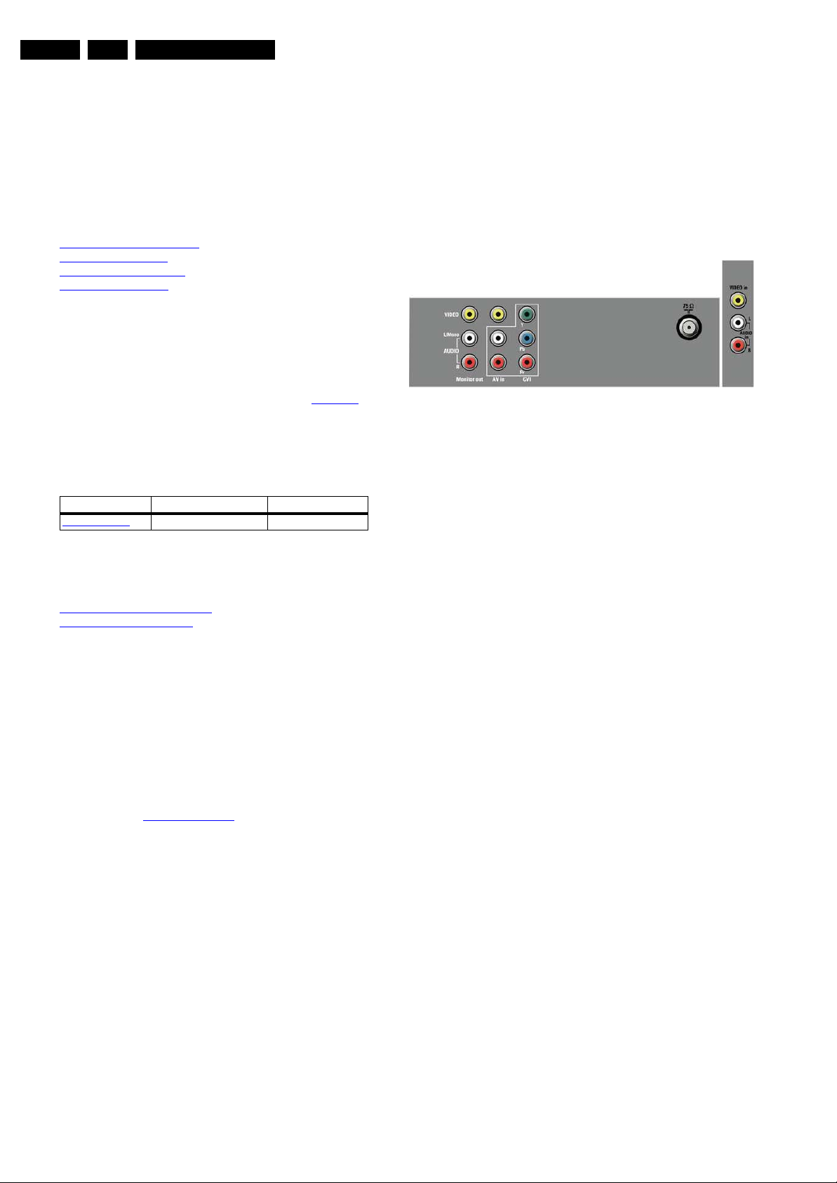
2.3.1 Connections
Figure 2-1 Rear and front connections
Monitor out cinch: Video CVBS - Out, Audio - Out
Ye - Video CVBS 1 V
Wh - Audio L 0.5 V
Rd - Audio R 0.5 V
AV in cinch: Video CVBS - In, Audio - In
Ye - Video CVBS 1 V
Wh - Audio L 0.5 V
Rd - Audio R 0.5 V
CVI in cinch: Video YPbPr - In
Gn - Video Y 1 V
Bu - Video Pb 0.7 V
Rd - Video Pr 0.7 V
/ 75 ohm kq
PP
/10 kohm kq
RMS
/ 10 kohm kq
RMS
/ 75 ohm jq
PP
/ 10 kohm jq
RMS
/ 10 kohm jq
RMS
/ 75 ohm jq
PP
/ 75 ohm jq
PP
/ 75 ohm jq
PP
2.3 Connection Overview
Note: The following connector color abbreviations are used
(acc. to DIN/IEC 757): Bk= Black, Bu= Blue, Gn= Green, Gy=
Grey, Rd= Red, Wh= White, and Ye= Yellow.
2.4 Chassis Overview
Refer to chapter 9. Block Diagrams for PWB/CBA locations.
Aerial - In
- - F-connector Coax, 75 ohm D
Front in cinch: Video CVBS - In, Audio - In
Ye - Video CVBS 1 V
Wh - Audio L 0.5 V
Rd - Audio R 0.5 V
/ 75 ohm jq
PP
/ 10 kohm jq
RMS
/ 10 kohm jq
RMS
2010-Apr-16
Page 3
Precautions, Notes, and Abbreviation List
3. Precautions, Notes, and Abbreviation List
EN 3SK7.0L CA 3.
Index of this chapter:
3.1 Safety Instructions
3.2 Maintenance Instructions
3.3 Warnings
3.4 Notes
3.5 Abbreviation List
3.1 Safety Instructions
Safety regulations require the following during a repair:
• Connect the set to the Mains/AC Power via an isolation
transformer (> 800 VA).
• Replace safety components, indicated by the symbol h,
only by components identical to the original ones. Any
other component substitution (other than original type) may
increase risk of fire or electrical shock hazard.
• Wear safety goggles when you replace the CRT.
Safety regulations require that after a repair, the set must be
returned in its original condition. Pay in particular attention to
the following points:
• General repair instruction: as a strict precaution, we advise
you to re-solder the solder connections through which the
horizontal deflection current flows. In particular this is valid
for the:
1. Pins of the line output transformer (LOT).
2. Fly-back capacitor(s).
3. S-correction capacitor(s).
4. Line output transistor.
5. Pins of the connector with wires to the deflection coil.
6. Other components through which the deflection current
flows.
Note: This re-soldering is advised to prevent bad connections
due to metal fatigue in solder connections, and is therefore only
necessary for television sets more than two years old.
• Route the wire trees and EHT cable correctly and secure
them with the mounted cable clamps.
• Check the insulation of the Mains/AC Power lead for
external damage.
• Check the strain relief of the Mains/AC Power cord for
proper function, to prevent the cord from touching the CRT,
hot components, or heat sinks.
• Check the electrical DC resistance between the Mains/AC
Power plug and the secondary side (only for sets that have
a Mains/AC Power isolated power supply):
1. Unplug the Mains/AC Power cord and connect a wire
between the two pins of the Mains/AC Power plug.
2. Set the Mains/AC Power switch to the "on" position
(keep the Mains/AC Power cord unplugged!).
3. Measure the resistance value between the pins of the
Mains/AC Power plug and the metal shielding of the
tuner or the aerial connection on the set. The reading
should be between 4.5 Mohm and 12 Mohm.
4. Switch "off" the set, and remove the wire between the
two pins of the Mains/AC Power plug.
• Check the cabinet for defects, to prevent touching of any
inner parts by the customer.
3.2 Maintenance Instructions
We recommend a maintenance inspection carried out by
qualified service personnel. The interval depends on the usage
conditions:
• When a customer uses the set under normal
circumstances, for example in a living room, the
recommended interval is three to five years.
• When a customer uses the set in an environment with
higher dust, grease, or moisture levels, for example in a
kitchen, the recommended interval is one year.
• The maintenance inspection includes the following actions:
1. Perform the “general repair instruction” noted above.
2. Clean the power supply and deflection circuitry on the
chassis.
3. Clean the picture tube panel and the neck of the picture
tube.
3.3 Warnings
• In order to prevent damage to ICs and transistors, avoid all
high voltage flashovers. In order to prevent damage to the
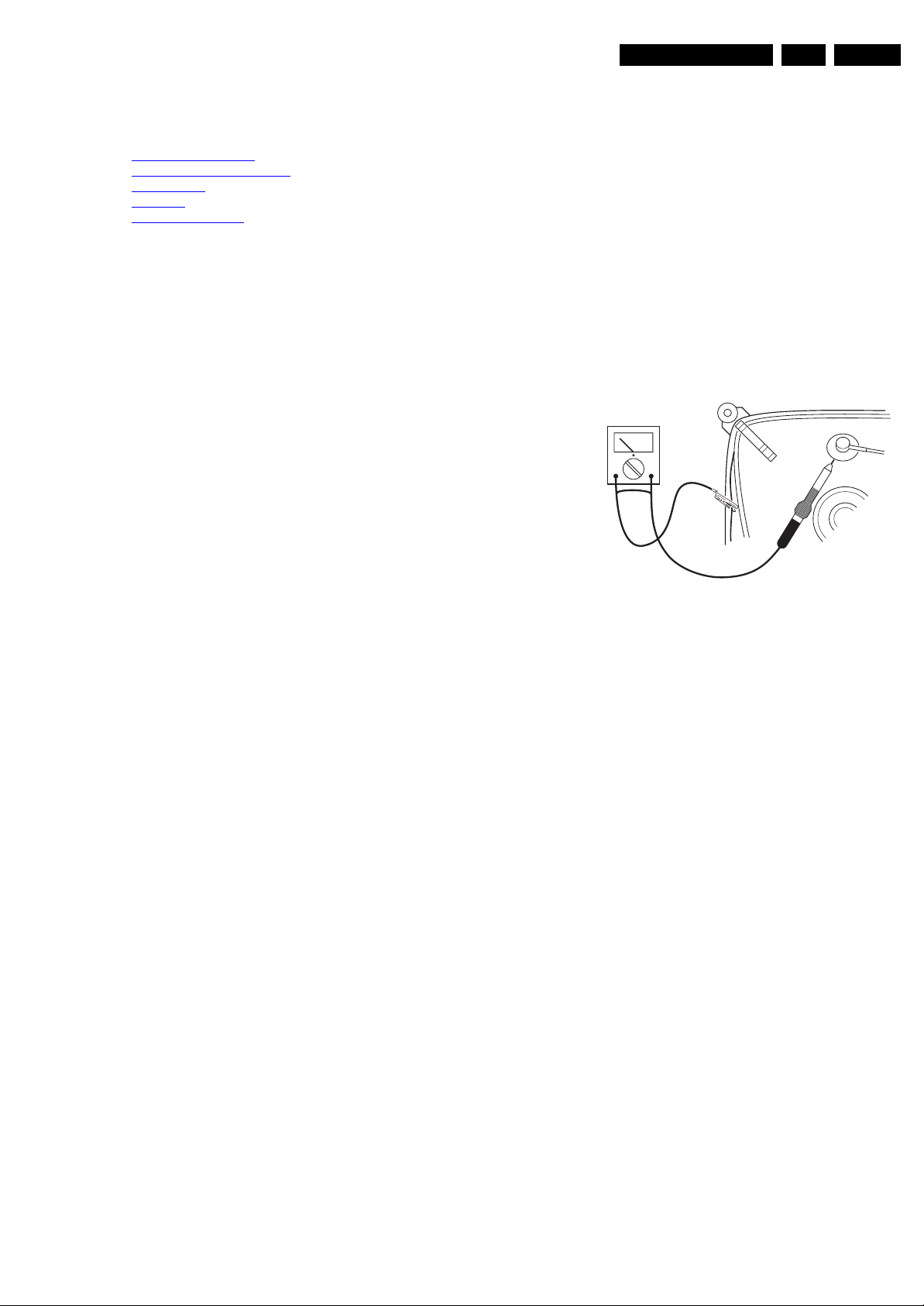
picture tube, use the method shown in figure “Discharge
picture tube”, to discharge the picture tube. Use a high
voltage probe and a multi-meter (position V
until the meter reading is 0 V (after approx. 30 s).
V
Figure 3-1 Discharge picture tube
• All ICs and many other semiconductors are susceptible to
electrostatic discharges (ESD w). Careless handling
during repair can reduce life drastically. Make sure that,
during repair, you are connected with the same potential as
the mass of the set by a wristband with resistance. Keep
components and tools also at this same potential.
• Be careful during measurements in the high voltage
section.
• Never replace modules or other components while the unit
is switched "on".
• When you align the set, use plastic rather than metal tools.
This will prevent any short circuits and prevents circuits
from becoming unstable.
3.4 Notes
3.4.1 General
• Measure the voltages and waveforms with regard to the
chassis (= tuner) ground (H), or hot ground (I), depending
on the tested area of circuitry. The voltages and waveforms
shown in the diagrams are indicative. Measure them in the
Service Default Mode (see chapter 5) with a color bar
signal and stereo sound (L: 3 kHz, R: 1 kHz unless stated
otherwise) and picture carrier at 475.25 MHz for PAL, or
61.25 MHz for NTSC (channel 3).
• Where necessary, measure the waveforms and voltages
with (D) and without (E) aerial signal. Measure the
voltages in the power supply section both in normal
operation (G) and in stand-by (F). These values are
indicated by means of the appropriate symbols.
• The semiconductors indicated in the circuit diagram and in
the parts lists, are interchangeable per position with the
semiconductors in the unit, irrespective of the type
indication on these semiconductors.
• Manufactured under license from Dolby Laboratories.
“Dolby”, “Pro Logic” and the “double-D symbol”, are
trademarks of Dolby Laboratories.
). Discharge
DC
E_06532_007.eps
250304
2010-Apr-16
Page 4
EN 4 SK7.0L CA3.
Precautions, Notes, and Abbreviation List
3.4.2 Schematic Notes
• All resistor values are in ohms, and the value multiplier is
often used to indicate the decimal point location (e.g. 2K2
indicates 2.2 kohm).
• Resistor values with no multiplier may be indicated with
either an "E" or an "R" (e.g. 220E or 220R indicates 220
ohm).
• All capacitor values are given in micro-farads (μ= x10
nano-farads (n= x10
-9
), or pico-farads (p= x10
• Capacitor values may also use the value multiplier as the
decimal point indication (e.g. 2p2 indicates 2.2 pF).
• An "asterisk" (*) indicates component usage varies. Refer
to the diversity tables for the correct values.
• The correct component values are listed in the Spare Parts
List. Therefore, always check this list when there is any
doubt.
3.4.3 Lead-free Soldering
Due to lead-free technology some rules have to be respected
by the workshop during a repair:
• Use only lead-free soldering tin Philips SAC305 with order
code 0622 149 00106. If lead-free solder paste is required,
please contact the manufacturer of your soldering
equipment. In general, use of solder paste within
workshops should be avoided because paste is not easy to
store and to handle.
• Use only adequate solder tools applicable for lead-free
soldering tin. The solder tool must be able:
– To reach a solder-tip temperature of at least 400°C.
– To stabilize the adjusted temperature at the solder-tip.
– To exchange solder-tips for different applications.
• Adjust your solder tool so that a temperature of around
360°C - 380°C is reached and stabilized at the solder joint.
Heating time of the solder-joint should not exceed ~ 4 sec.
Avoid temperatures above 400°C, otherwise wear-out of
tips will increase drastically and flux-fluid will be destroyed.
To avoid wear-out of tips, switch “off” unused equipment or
reduce heat.
• Mix of lead-free soldering tin/parts with leaded soldering
tin/parts is possible but PHILIPS recommends strongly to
avoid mixed regimes. If this cannot be avoided, carefully
clear the solder-joint from old tin and re-solder with new tin.
3.4.4 Alternative BOM identification
The third digit in the serial number (example:
AG2B0335000001) indicates the number of the alternative
B.O.M. (Bill Of Materials) that has been used for producing the
specific TV set. In general, it is possible that the same TV
model on the market is produced with e.g. two different types
of displays, coming from two different suppliers. This will then
result in sets which have the same CTN (Commercial Type
Number; e.g. 28PW9515/12) but which have a different B.O.M.
number.
By looking at the third digit of the serial number, one can
identify which B.O.M. is used for the TV set he is working with.
If the third digit of the serial number contains the number “1”
(example: AG1B033500001), then the TV set has been
manufactured according to B.O.M. number 1. If the third digit is
a “2” (example: AG2B0335000001), then the set has been
produced according to B.O.M. no. 2. This is important for
ordering the correct spare parts!
For the third digit, the numbers 1...9 and the characters A...Z
can be used, so in total: 9 plus 26= 35 different B.O.M.s can be
indicated by the third digit of the serial number.
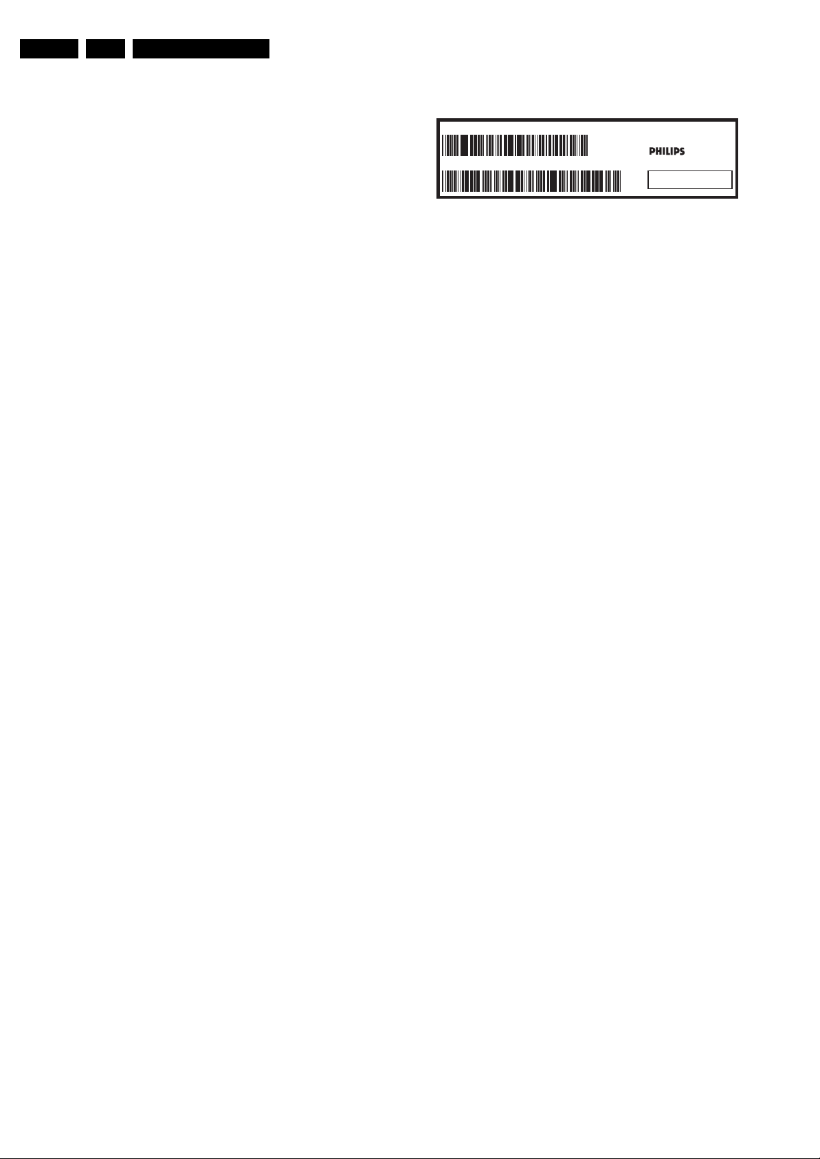
Identification: The bottom line of a type plate gives a 14-digit
serial number. Digits 1 and 2 refer to the production center (e.g.
AG is Bruges), digit 3 refers to the B.O.M. code, digit 4 refers
to the Service version change code, digits 5 and 6 refer to the
production year, and digits 7 and 8 refer to production week (in
2010-Apr-16
-12
example below it is 2006 week 17). The 6 last digits contain the
serial number.
MODEL :
PROD.NO:
-6
),
32PF9968/10
AG 1A0617 000001
).
MADE IN BELGIUM
220-240V 50/60Hz
~
VHF+S+H+UHF
BJ3.0E LA
S
128W
E_06532_024.eps
260308
Figure 3-2 Serial number (example)
3.4.5 Board Level Repair (BLR) or Component Level Repair (CLR)
If a board is defective, consult your repair procedure to decide
if the board has to be exchanged or if it should be repaired on
component level.
If your repair procedure says the board should be exchanged
completely, do not solder on the defective board. Otherwise, it
cannot be returned to the O.E.M. supplier for back charging!
3.4.6 Practical Service Precautions
• It makes sense to avoid exposure to electrical shock.
While some sources are expected to have a possible
dangerous impact, others of quite high potential are of
limited current and are sometimes held in less regard.
• Always respect voltages. While some may not be
dangerous in themselves, they can cause unexpected
reactions that are best avoided. Before reaching into a
powered TV set, it is best to test the high voltage insulation.
It is easy to do, and is a good service precaution.
3.5 Abbreviation List
0/6/12 SCART switch control signal on A/V
board. 0 = loop through (AUX to TV),
6 = play 16 : 9 format, 12 = play 4 : 3
format
AARA Automatic Aspect Ratio Adaptation:
ACI Automatic Channel Installation:
ADC Analogue to Digital Converter
AFC Automatic Frequency Control: control
AGC Automatic Gain Control: algorithm that
AM Amplitude Modulation
AP Asia Pacific
AR Aspect Ratio: 4 by 3 or 16 by 9
ASF Auto Screen Fit: algorithm that adapts
ATSC Advanced Television Systems
ATV See Auto TV
Auto TV A hardware and software control
AV External Audio Video
AVC Audio Video Controller
algorithm that adapts aspect ratio to
remove horizontal black bars; keeps
the original aspect ratio
algorithm that installs TV channels
directly from a cable network by
means of a predefined TXT page
signal used to tune to the correct
frequency
controls the video input of the feature
box
aspect ratio to remove horizontal black
bars without discarding video
information
Committee, the digital TV standard in
the USA
system that measures picture content,
and adapts image parameters in a
dynamic way
Page 5

Precautions, Notes, and Abbreviation List
EN 5SK7.0L CA 3.
AVIP Audio Video Input Processor
B/G Monochrome TV system. Sound
carrier distance is 5.5 MHz
BLR Board-Level Repair
BTSC Broadcast Television Standard
Committee. Multiplex FM stereo sound
system, originating from the USA and
used e.g. in LATAM and AP-NTSC
countries
B-TXT Blue TeleteXT
C Centre channel (audio)
CEC Consumer Electronics Control bus:
remote control bus on HDMI
connections
CL Constant Level: audio output to
connect with an external amplifier
CLR Component Level Repair
ComPair Computer aided rePair
CP Connected Planet / Copy Protection
CSM Customer Service Mode
CTI Color Transient Improvement:
manipulates steepness of chroma
transients
CVBS Composite Video Blanking and
Synchronization
DAC Digital to Analogue Converter
DBE Dynamic Bass Enhancement: extra
low frequency amplification
DDC See “E-DDC”
D/K Monochrome TV system. Sound
carrier distance is 6.5 MHz
DFI Dynamic Frame Insertion
DFU Directions For Use: owner's manual
DMR Digital Media Reader: card reader
DMSD Digital Multi Standard Decoding
DNM Digital Natural Motion
DNR Digital Noise Reduction: noise
reduction feature of the set
DRAM Dynamic RAM
DRM Digital Rights Management
DSP Digital Signal Processing
DST Dealer Service Tool: special remote
control designed for service
technicians
DTCP Digital Transmission Content
Protection; A protocol for protecting
digital audio/video content that is
traversing a high speed serial bus,
such as IEEE-1394
DVB-C Digital Video Broadcast - Cable
DVB-T Digital Video Broadcast - Terrestrial
DVD Digital Versatile Disc
DVI(-d) Digital Visual Interface (d= digital only)
E-DDC Enhanced Display Data Channel
(VESA standard for communication
channel and display). Using E-DDC,
the video source can read the EDID
information form the display.
EDID Extended Display Identification Data
(VESA standard)
EEPROM Electrically Erasable and
Programmable Read Only Memory
EMI Electro Magnetic Interference
EPLD Erasable Programmable Logic Device
EU Europe
EXT EXTernal (source), entering the set by
SCART or by cinches (jacks)
FDS Full Dual Screen (same as FDW)
FDW Full Dual Window (same as FDS)
FLASH FLASH memory
FM Field Memory or Frequency
Modulation
FPGA Field-Programmable Gate Array
FTV Flat TeleVision
Gb/s Giga bits per second
G-TXT Green TeleteXT
H H_sync to the module
HD High Definition
HDD Hard Disk Drive
HDCP High-bandwidth Digital Content
Protection: A “key” encoded into the
HDMI/DVI signal that prevents video
data piracy. If a source is HDCP coded
and connected via HDMI/DVI without
the proper HDCP decoding, the
picture is put into a “snow vision” mode
or changed to a low resolution. For
normal content distribution the source
and the display device must be
enabled for HDCP “software key”
decoding.
HDMI High Definition Multimedia Interface
HP HeadPhone
I Monochrome TV system. Sound
2
I
C Inter IC bus
2
I
D Inter IC Data bus
2
I
S Inter IC Sound bus
carrier distance is 6.0 MHz
IF Intermediate Frequency
IR Infra Red
IRQ Interrupt Request
ITU-656 The ITU Radio communication Sector
(ITU-R) is a standards body
subcommittee of the International
Telecommunication Union relating to
radio communication. ITU-656 (a.k.a.
SDI), is a digitized video format used
for broadcast grade video.
Uncompressed digital component or
digital composite signals can be used.
The SDI signal is self-synchronizing,
uses 8 bit or 10 bit data words, and has
a maximum data rate of 270 Mbit/s,
with a minimum bandwidth of 135
MHz.
ITV Institutional TeleVision; TV sets for
hotels, hospitals etc.
LS Last Status; The settings last chosen
by the customer and read and stored
in RAM or in the NVM. They are called
at start-up of the set to configure it
according to the customer's
preferences
LATAM Latin America
LCD Liquid Crystal Display
LED Light Emitting Diode
L/L' Monochrome TV system. Sound
carrier distance is 6.5 MHz. L' is Band
I, L is all bands except for Band I
LPL LG.Philips LCD (supplier)
LS Loudspeaker
LVDS Low Voltage Differential Signalling
Mbps Mega bits per second
M/N Monochrome TV system. Sound
carrier distance is 4.5 MHz
MIPS Microprocessor without Interlocked
Pipeline-Stages; A RISC-based
microprocessor
MOP Matrix Output Processor
MOSFET Metal Oxide Silicon Field Effect
Transistor, switching device
MPEG Motion Pictures Experts Group
MPIF Multi Platform InterFace
MUTE MUTE Line
NC Not Connected
NICAM Near Instantaneous Compounded
Audio Multiplexing. This is a digital
sound system, mainly used in Europe.
NTC Negative Temperature Coefficient,
non-linear resistor
2010-Apr-16
Page 6

EN 6 SK7.0L CA3.
Precautions, Notes, and Abbreviation List
NTSC National Television Standard
Committee. Color system mainly used
in North America and Japan. Color
carrier NTSC M/N= 3.579545 MHz,
NTSC 4.43= 4.433619 MHz (this is a
VCR norm, it is not transmitted off-air)
NVM Non-Volatile Memory: IC containing
TV related data such as alignments
O/C Open Circuit
OSD On Screen Display
OTC On screen display Teletext and
Control; also called Artistic (SAA5800)
P50 Project 50: communication protocol
between TV and peripherals
PAL Phase Alternating Line. Color system
mainly used in West Europe (color
carrier= 4.433619 MHz) and South
America (color carrier PAL M=
3.575612 MHz and PAL N= 3.582056
MHz)
PCB Printed Circuit Board (same as “PWB”)
PCM Pulse Code Modulation
PDP Plasma Display Panel
PFC Power Factor Corrector (or Pre-
conditioner)
PIP Picture In Picture
PLL Phase Locked Loop. Used for e.g.
FST tuning systems. The customer
can give directly the desired frequency
POD Point Of Deployment: a removable
CAM module, implementing the CA
system for a host (e.g. a TV-set)
POR Power On Reset, signal to reset the uP
PTC Positive Temperature Coefficient,
non-linear resistor
PWB Printed Wiring Board (same as “PCB”)
PWM Pulse Width Modulation
QRC Quasi Resonant Converter
QTNR Quality Temporal Noise Reduction
QVCP Quality Video Composition Processor
RAM Random Access Memory
RGB Red, Green, and Blue. The primary
color signals for TV. By mixing levels
of R, G, and B, all colors (Y/C) are
reproduced.
RC Remote Control
RC5 / RC6 Signal protocol from the remote
control receiver
RESET RESET signal
ROM Read Only Memory
RSDS Reduced Swing Differential Signalling
data interface
R-TXT Red TeleteXT
SAM Service Alignment Mode
S/C Short Circuit
SCART Syndicat des Constructeurs
d'Appareils Radiorécepteurs et
SCL Serial Clock I
Téléviseurs
SCL-F CLock Signal on Fast I
SD Standard Definition
SDA Serial Data I
SDA-F DAta Signal on Fast I
2
C
2
C bus
2
C
2
C bus
SDI Serial Digital Interface, see “ITU-656”
SDRAM Synchronous DRAM
SECAM SEequence Couleur Avec Mémoire.
Color system mainly used in France
and East Europe. Color carriers=
4.406250 MHz and 4.250000 MHz
SIF Sound Intermediate Frequency
SMPS Switched Mode Power Supply
SoC System on Chip
SOG Sync On Green
SOPS Self Oscillating Power Supply
SPI Serial Peripheral Interface bus; a 4-
wire synchronous serial data link
standard
S/PDIF Sony Philips Digital InterFace
SRAM Static RAM
SRP Service Reference Protocol
SSB Small Signal Board
STBY STand-BY
SVGA 800 × 600 (4:3)
SVHS Super Video Home System
SW Software
SWAN Spatial temporal Weighted Averaging
Noise reduction
SXGA 1280 × 1024
TFT Thin Film Transistor
THD Total Harmonic Distortion
TMDS Transmission Minimized Differential
Signalling
TXT TeleteXT
TXT-DW Dual Window with TeleteXT
UI User Interface
uP Microprocessor
UXGA 1 600 × 1 200 (4:3)
V V-sync to the module
VESA Video Electronics Standards
Association
VGA 640 × 480 (4:3)
VL Variable Level out: processed audio
output toward external amplifier
VSB Vestigial Side Band; modulation
method
WYSIWYR What You See Is What You Record:
record selection that follows main
picture and sound
WXGA 1280 × 768 (15:9)
XTAL Quartz crystal
XGA 1024 × 768 (4:3)
Y Luminance signal
Y/C Luminance (Y) and Chrominance (C)
signal
YPbPr Component video. Luminance and
scaled color difference signals (B-Y
and R-Y)
YUV Component video
2010-Apr-16
Page 7
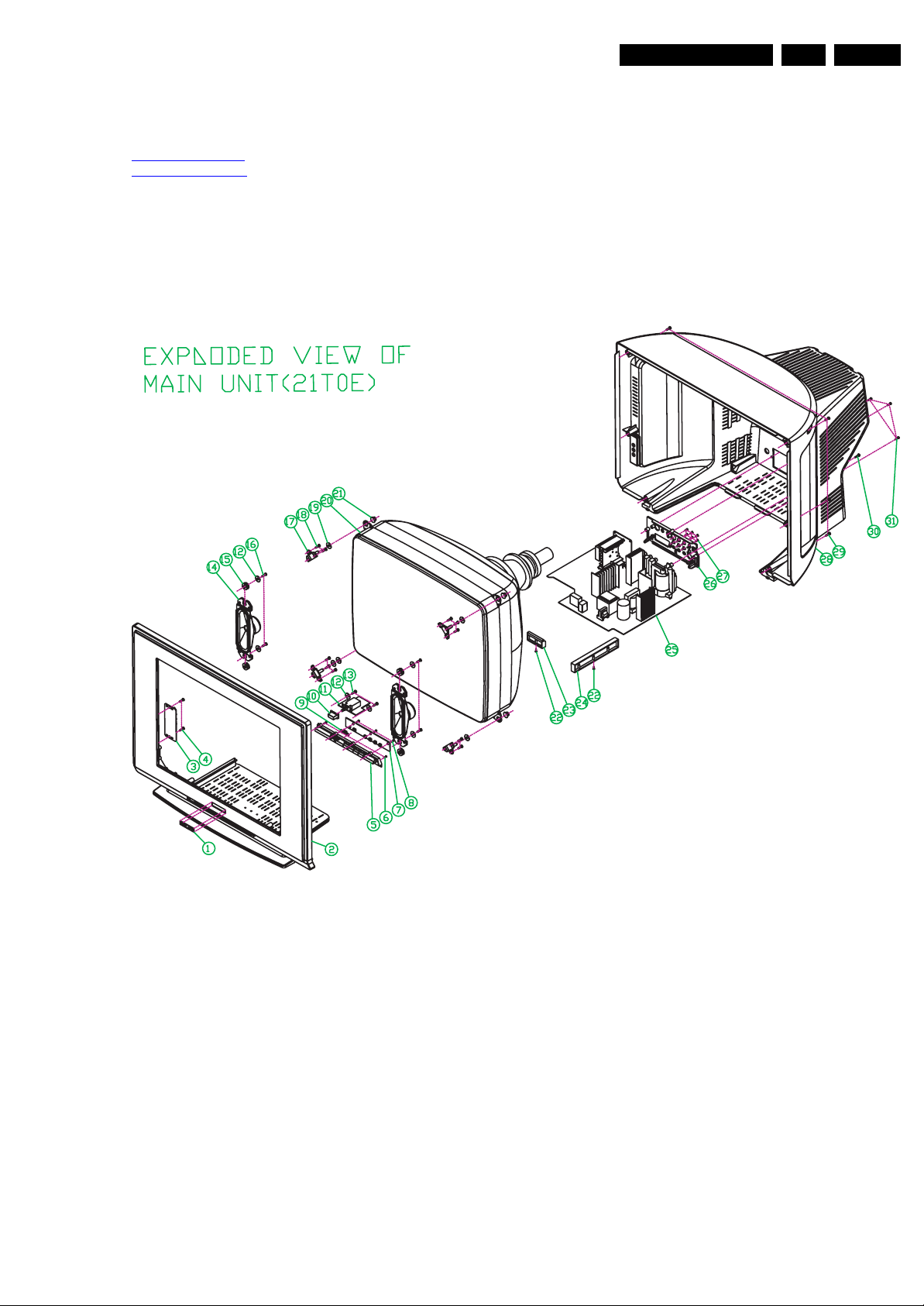
4. Mechanical Instructions
Mechanical Instructions
EN 7SK7.0L CA 4.
Index of this chapter:
4.1 Set Disassembly
4.2 Set Re-assembly
Note: Figures below can deviate slightly from the actual
situation, due to the different set executions.
4.1 Set Disassembly
Follow the disassemble instructions in described order.
4.1.1 Rear Cover Removal
Warning: disconnect the mains power cord before you remove
the rear cover.
1. Remove all the fixation screws of the rear cover.
2. Now, pull the rear cover backwards and remove it.
4.2 Set Re-assembly
To re-assemble the whole set, do all processes in reverse
order.
Be sure that, before the rear cover is mounted:
• The mains cord is positioned correctly in its guiding
brackets (make sure that the strain reliefs are replaced in
its correct position and that it will function correctly!).
• All wires/cables are returned in their original positions.
Figure 4-1 Set Disassembly SL7 styling
2010-Apr-16
Page 8

EN 8 SK7.0L CA5.
Service Modes, Error Codes, and Fault Finding
5. Service Modes, Error Codes, and Fault Finding
Index of this chapter:
5.1 Test Points
5.2 Service Modes
5.3 Error Codes
5.4 Fault Finding
5.1 Test Points
See chapter 9 Blockdiagrams.
Perform measurements under the following conditions:
• Service Default Mode.
• Video: color bar signal.
• Audio: 3 kHz left, 1 kHz right.
5.2 Service Modes
This chassis does not contain a specific Service Mode. Service
and Alignment of the TV set can be done via the Factory Mode
by the service technician, see chapter 6.
5.3 Error Codes
Not applicable.
5.4 Fault Finding
5.4.7 Picture with Horizontal Bright Line and Sound
Check both supply voltages of vertical IC301 and relevant
circuitry on correctness and the vertical synchronizing signal.
5.4.8 Remote Control Malfunction
Check the supply voltage of IR receiver. The normal value
should be 5.15 V. If this is correct check front control panels
soldering connections. If can't be solved, check the remote
control, crystal or transmitting diode of the remote control are
in good condition.
5.4.9 No Sound
Check power supply of sound IC (IC401) and relevant circuitry.
Check as well the BTSC board (if present), check the power
supply of IC801 and relevant output signal pins 21 and 27 of
this IC. Do not exclude IC801 and/or IC401 to be defective. If
needed replace the speakers.
5.4.10 Poor Sound Quality
Check the sound system after searching the channel which
should set at NTSC or AUTO. If still has problem, check
accompany board circuit on chassis good or not.
5.4.1 Power on Failure
Check whether the power supply is working properly and
whether the values of voltages normal. If those are correct,
check line transistor and transformer are working properly or
check fore or back line for defects.
5.4.2 Horizontal Deflection Transistor Defective: No Picture, No Sound.
To find the fault for a defect horizontal deflection transistor
please check the following items:
• Over voltage to breakdown.
• Over current to burn.
• Horizontal frequency too low.
• Horizontal drive inefficient.
5.4.3 Picture Interference
• Check if the signal line contact is good.
• Change Tuner if is necessary.
5.4.4 Cannot find any TV program
Checking method: Check the closed circuit from tuner to
picture decoder IC to detect whether there are defective
components.
5.4.5 No Good Picture or Double Image
Check the correctness of the signal from IF to Q102 and
relevant circuit. In this case the problem can be Q102 and/or
SAW201.
5.4.6 Picture not or incorrect Colored
• Check the circuit from IC201 to R.G.B. three gun circuit.
• Check the IC soldering and relevant circuitry on physical
damage or check for defective capacitors.
2010-Apr-16
Page 9

6. Alignments
Alignments
EN 9SK7.0L CA 6.
Index of this chapter:
6.1 General Alignment Conditions
6.2 Software Alignments
6.3 Factory mode Settings
6.1 General Alignment Conditions
6.1.1 Default Alignment Settings
Perform all electrical adjustments under the following
conditions:
• Power supply voltage: 230 V
• Connect the set to the mains via an isolation transformer
with low internal resistance.
• Allow the set to warm up for approximately 20 to 30
minutes.
• Measure voltages and waveforms in relation to chassis
ground (with the exception of the voltages on the primary
side of the power supply).
Caution: never use heatsinks as ground.
• Test probe: 100: 1, Ri > 10 Mohm, Ci < 3.5 pF.
• Use an isolated trimmer/screwdriver to perform
alignments.
/ 50 Hz (± 10%).
AC
6.2 Software Alignments
Put the set in its MENU mode (factory mode) as follows (see
also figure “Factory Mode” on the next page):
• Press the keys [i+], “smart sound” and “smart picture” to
enter the factory menu.
• Press the keys [i+] again and “ADJUST” appear on screen.
• Press the number keys to enter the adjust page, press B /
y to choose the items that to be adjusted, Press z /A to
adjust its value.
• Press [i+] to quit factory mode.
The different alignment parameters are described further on.
2. Press key “0” and adjust “HPH” to set picture horizontal
centre to CRT horizontal centre.
6.2.5 Vertical & YUV/RGB Horizontal Adjust (Key 0)
1. Provide a 50 Hz cross hatch signal, set TV to standard
mode. Adjust VSL so that half picture of the pane cross
appears. The picture’s vertical line and kinescope are in
superposition.
2. Adjust VSI to obtain picture’s vertical re-display ratio more
than 90%.
3. Provide a 60 Hz cross hatch signal, do step 1 and 2 again
to adjust.
4. If necessary, fine adjust above items.
6.2.1 Rf AGC Voltage Adjust
1. Provide a 571.25 MHz, 60 dB half color bar signal.
2. Enter factory service mode and press key 3.
3. Measure tuner AGC point voltage, adjust AGC item till the
voltage is 2.4 V, or till picture noise just disappears (typical
value is at 27).
6.2.2 Focus Fine Adjust
1. Provide a cross-hatch pattern signal.
2. Set state to “Rich” mode.
3. Adjust flyback transformers “Focus” knob till picture is
clear.
6.2.3 Screen Voltage Adjust (Key 0)
1. Set picture to “AV Standard” mode, without signal input.
2. Press the keys [i+], “Smart sound” and “Smart picture” to
enter the factory menu. Press key “3” to enter page 3.
When select “VG2” item, there will be a horizontal line or “in
high” “out of high” is displayed on the screen.
3. Adjust flyback transformers “Screen” knob till “OK” is
displayed on screen, or untill the horizontal line just can be
seen.
6.2.4 Horizontal Adjustment
1. Provide a 50 Hz monoscope pattern.
– Press the keys [i+], “Smart sound” and “Smart picture”
to enter the factory menu.
2010-Apr-16
Page 10
EN 10 SK7.0L CA6.
6.3 Factory mode Settings
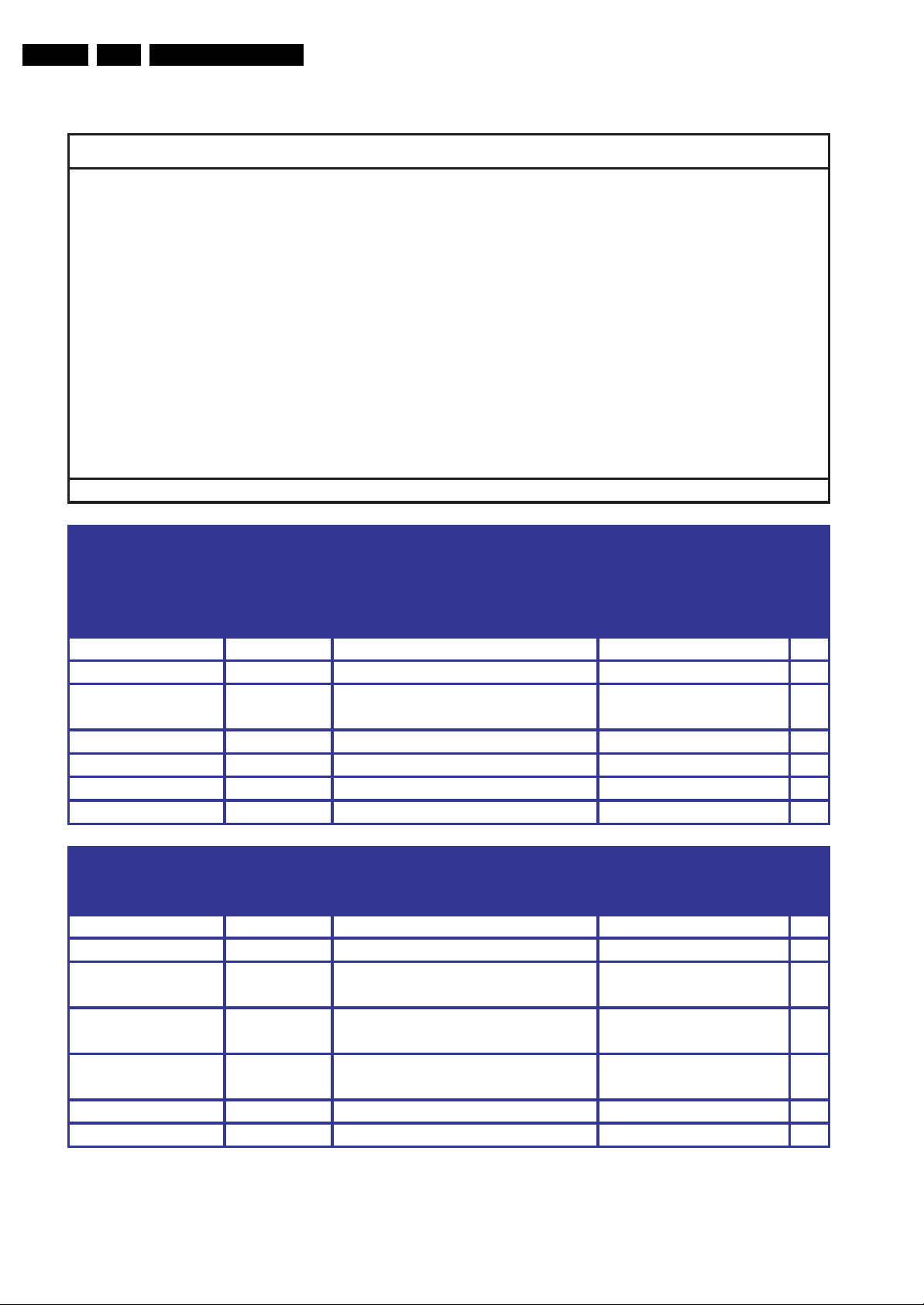
1ޔHow to enter and exit service mode:
Enter "factory service mode" 㧦press "Display", "Sound mode" and "PP" in turn.
Enter "design service mode" : aer entering "factory service mode", select "SC"item, then press "8", "9" keys.
Exit service mode: press"DISPLAY"key to exit service mode.
2ޔIn service mode, pressing digital keys directly can enter the corresponding page, pressing "MENU"key can
enter the next page.
Pressing "UP"and"DOWN"keys can select the items to adjust, pressing"LEFT"and"RIGHT"keys can adjust the
values.
3ޔBUS OPEN mode: In service mode, pressing"MUTE" key can enter "BUS OPEN" mode, which is useful for
white balance adjustment using AUTO WHITE BALANCE EQUIPMENT or mass data wrien into EEPROM IC.
Pressing"MUTE" can exit "BUS OPEN" mode.
4ޔFACTORY mode: In service mode, pressing"A/CH"key can enter "FACTORY MODE", which is useful for aging
in producon lines. Pressing "8" key and "9" key again can exit "FACTORY MODE"
Alignments
UOC TOP Service Item Description
Table 0 Gemometric Service seng 50Hz/60Hz
Service setting
OSD
Display
String
Description
Value
(Min…Max)
/Item list
Horizontal shi HSH Horizontal shi 0..63 32
EW width EWW East West Width 0..63 32
Vercal slope VSL
Vercal slope.This will switch screen
to half blank.
0..63 32
Vercal shi VSH Vercal shi 0..63 32
Vercal amplitude VAM Vercal amplitude 0..63 32
S-correcon SC S-correcon 0..63 32
Table 1 Geometric Service seng 1 50Hz/60Hz.
Service setting
OSD
Display
String
Description
Value
(Min…Max)
/Item list
EW parabola/width PW East West Parabola Width 0..63 32
EW trapezium TC East West Trapezium 0..63 32
Upper Corner
Parabola
Lower Corner
Parabola
Horizontal
parallelogram
UCP East West Upper Corner Parabola 0..63 32
LCP East West lower Corner Parabola 0..63 32
HPAR Horizontal parallelogram 0..63 32
Horizontal bow HBOW Horizontal bow 0..63 32
Default
Default
2010-Apr-16
Page 11
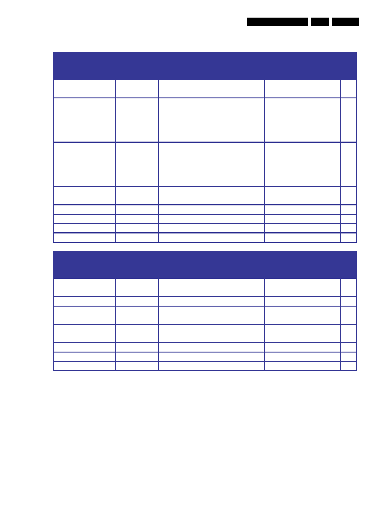
Table 2
Service setting
Black level
offset C
OSD
Display
String
BLOC
Description
Black level
offset Course
Alignments
EN 11SK7.0L CA 6.
Value
(Min…Max)
/Item list
0..63 7
Default
Black level
offset R
Black level
offset G
Black level
offset B
BLOR Black level offset Red 0..63 32
BLOG Black level offset Green 0..63 32
BLOB Black level offset Blue 0..63 32
White point R WPR White point Red 0..63 32
White point G WPG White point Green 0..63 32
White point B WPB White point BLUE 0..63 32
Table 3
OSD
Service setting
Display
String
AGC Take over AGC
Description
AGC Take over. Also used as TOP
when an internal AGC tuner is used.
Value
(Min…Max)
/Item list
0..63 32
Sub-brightness SUB-BRI Sub brightness 0..63 0
brightness of white
balance
contrast of white
balance
WBT
WCT
In TV or YUV,brightness of white
balance
In TV or YUV,brightness of white
contrast
0..63 32
0..63 32
VG2 VG2 VG2 Adjust 0..63 32
Out of factory BOX Out of factory 0..㧝 0
Default
2010-Apr-16
Page 12
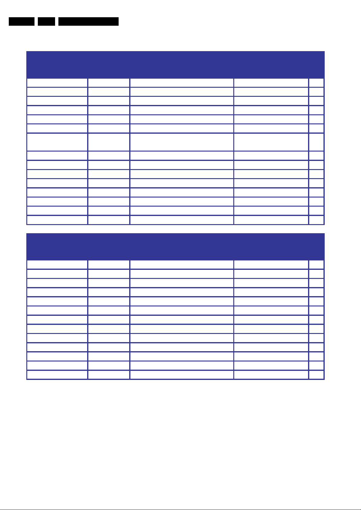
EN 12 SK7.0L CA6.
Alignments
Table 4 Gemometric Service seng 2
Service setting
OSD
Display
String
Description
Value
(Min…Max)
/Item list
Speech treble S-TR Speech treble 0..63 24
Speech bass S-BA Speech bass 0..63 42
Music treble M-TR Music treble 0..63 42
Music bass M-BA Music bass 0..63 48
Theatre treble T-TR Theatre treble 0..63 32
Theatre bass T-BA Theatre bass 0..63 48
AV curve offset
compare to TV
AV-OF AV curve offset compare to TV -31..32 0
Volume curve V-05 The volume seng for OSD 5 0..81 5
Volume curve V-10 The volume seng for OSD 10 0..81 15
Volume curve V-20 The volume seng for OSD 20 0..81 25
Volume curve V-30 The volume seng for OSD 30 0..81 35
Volume curve V-40 The volume seng for OSD 40 0..81 55
Volume curve V-50 The volume seng for OSD 50 0..81 65
Volume curve V-63 The volume seng for OSD 63 0..81 81
Default
Table 5
Service setting
OSD
Display
String
Description
Value
(Min…Max)
/Item list
So brightness S-BRI So brightness 0..63 32
So colour S-COL So colour 0..63 20
So contrast S-CON So contrast 0..63 20
So sharpness S-SHA So sharpness 0..63 25
Natural brightness N-BRI Natural brightness 0..63 32
Natural colour N-COL Natural colour 0..63 25
Natural contrast N-CON Natural contrast 0..63 21
Natural sharpness N-SHA Natural sharpness 0..63 32
Rich brightness R-BRI Rich brightness 0..63 38
Rich colour R-COL Rich colour 0..63 30
Rich contrast R-CON Rich contrast 0..63 50
Rich sharpness R-SHA Rich sharpness 0..63 20
Default
2010-Apr-16
Page 13
Alignments
EN 13SK7.0L CA 6.
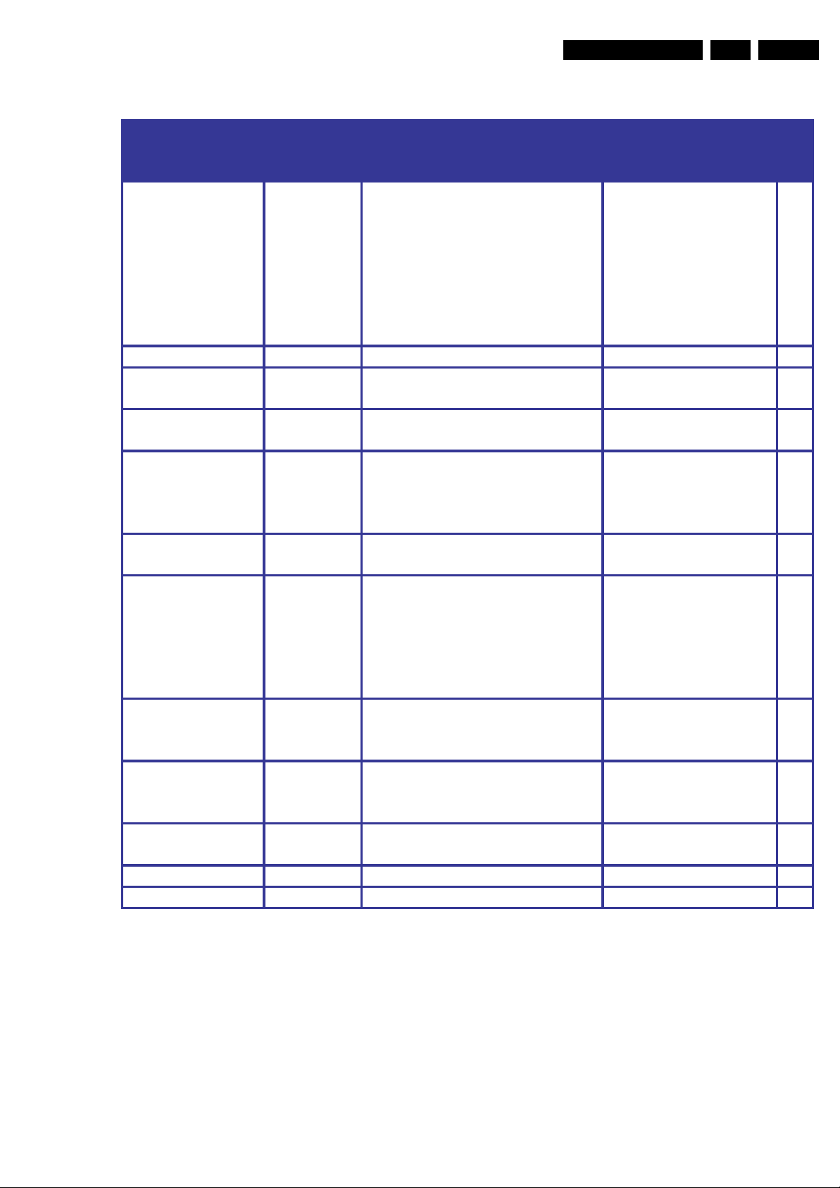
Table 6
Service setting
OSD
Display
String
Description
Value
(Min…Max)
/Item list
0:58.75M
1:45.75M
IFA, IFB, IFC IF IF select
2:38.9M
3:38,00M
4:33.40M
5:33.90M
AGC Speed A SPD AGC speed adjust 0..3 1
Blue screen B B Blue screen
Video mute V-M switch source whether blanking
0:No signal is snowflake
1:No signal is blue screen
0:No black blanking
1:blanking
0:MUTE low
mute pin type M-MODE mute pin type
DEMUTE high
1:MUTE high
DEMUTE low
AV POC SETTING A-POC AV POC SETTING
0:POC=0
1:POC by IFI seng
0:POC by LOCK or SL
seng
TV POC SETTING T-POC TV POC SETTING
1:POC by LOCK or IFI
seng
2:POC by LOCK or IFI or SL
seng
Default
1
1
1
0
1
1
0:AV by IFI seng,TV by IFI
bule scree condion BULE bule scree condion
or SL seng
1
1:Program seng
0:Program seng
switch off condion OFF switch off condion
1:AV by IFI seng,TV by IFI
1
and SL seng
VG2-MODE VG2-MODE
0:Light line adjust mode
1:Character adjust mode
0..1 0
VSD-Bri VSD-Bri VG2 brightness adjust 0..63 32
CC-DELAY DELAY CCD delay 0..127 2
2010-Apr-16
Page 14
EN 14 SK7.0L CA6.
Alignments
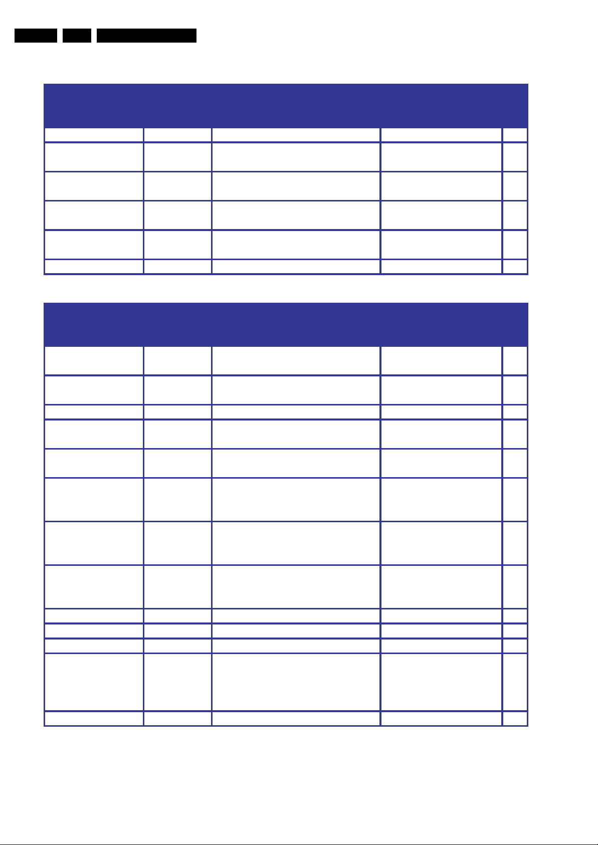
Table 7
Service setting
OSD
Display
String
Description
Value
(Min…Max)
/Item list
BTSC-MODE MODE BTSC mode select 0..2 0
SAP SEND LO OR HI SAP-LH SAP SEND LO OR HI
STEREO SENS LO OR
HI
STEREO-LH STEREO SENS LO OR HI
SAP Level 1 or 2 SAP1-2 SAP Level 1 or 2
SIF or BASE BAND
mode
SIF-BASE SIF or BASE BAND mode
0:SAP low
1:SAP high
0:STEREO low
1:STEREO high
0:SAP level 1
1:SAP level 2
0:SIF mode
1:BASE BAND mode
BTSC-DETECT DETECT BTSC detect me for switch source 50
Table 8
OSD
Service setting
Display
Description
String
Bass and treble BAS-TRE
Bass and treble present in sound
menu
DSK register DSK Dynamic skin control on/off
Value
(Min…Max)
/Item list
0:Off
1:On
0:Off
1:On
Disco Gain DISG register DISG 0x4a bit 6 0/1 0
Coring of SVM
output sigle
Cap bank switch
for DCXO
COF Register COFF 0x48 bit 7 0/1 0
DCXO NTSC DCXO_CAP seng 0..3 2
PAL-M Cap bank
switch
PM-DCXO PAL-M DCXO_CAP seng 0..3 2
for DCXO
PAL-N Cap bank
switch
PN-DCXO PAL-N DCXO_CAP seng 0..3 2
for DCXO
0:AKB seng 0,have CCC
AKB AKB AKB register seng
funcon
1:AKB seng 1
OSD Positon O-V50 OSD vercal positon for 50HZ 0..63 35
OSD Positon O-V60 OSD vercal positon for 60HZ 0..63 35
OSD Positon O-HOR OSD Horizontal positon 10..50 36
0..2
PCB Logic LOGIC PCB Logic
0:3P67SN
1:5P67SN
2:3P69SN
Init NVM INIT Init NVM 0/1 0
Default
0
0
0
1
Default
0
0
1
1
2010-Apr-16
Page 15
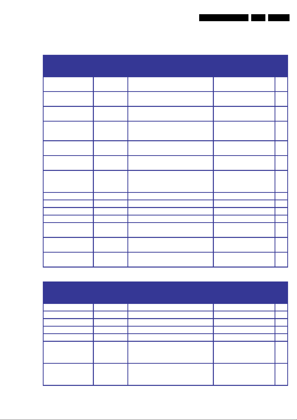
Table 9
Alignments
EN 15SK7.0L CA 6.
OSD
Service setting
Display
Description
String
AV1 AV1 AV1 present for AV status
SIDE SIDE SIDE present for AV status
AV2 AV2 AV2 present for AV status
S-VIDEO S-V S-VIDEO present for AV status
YUV YUV YUV present for AV status
Le sound output MONO TV MONO select
Value
(Min…Max)
/Item list
0:Off
1:On
0:Off
1:On
0:Off
1:On
0:Off
1:On
0:Off
1:On
0:stereo
1:mono
1
1
0
0
0
0
0:power on
Standby remember R-POWER Standby remember
1:power off
0
2:power remember
Vercal linearity 5VLIN Vercal linearity for 50 Hz 0..63 32
Vercal linearity 6VLIN Vercal linearity for 60 Hz 0..63 32
VCS 5VSCR Vercal scroll for 50 Hz 0..63 32
VCS 6VSCR Vercal scroll for 60 Hz 0..63 32
VX or VA seng
when 16:9 nide
ZOOM 16
4:3 ZOOM N
Expand 4:3 ZOOM EX
VX-VAM=0,Seng VX register
VX-VAM=1,Seng VA register
VX-VAM=0,Seng VX register
VX-VAM=1,Seng VA register
VX-VAM=0,Seng VX register
VX-VAM=1,Seng VA register
0..63 0
0..63 25
0..63 51
Default
Table 10
Service setting
OSD
Display
String
Description
Value
(Min…Max)
/Item list
Max-brightness MAX-BRI Max-brightness 0..63 63
Sub-contrast SUB-CON Sub-contrast 0..63 0
Max-contrast MAX-CON Max-contrast 0..63 63
Max-colour MAX-COL Max-colour 0..63 63
No signal EWW N-EWW No signal EWW -32..+31 0
0..1
Black stretch depth DEP Black stretch depth
0:15 IRE
0
1:30 IRE
0:normal
Color temp of so S-C Color temp of so
1:cold
2
2:warm
2010-Apr-16
Default
Page 16
EN 16 SK7.0L CA6.
Alignments
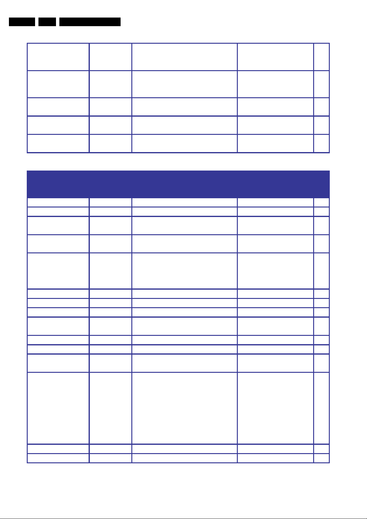
0:normal
Color temp of nature N-C Color temp of nature
1:cold
2:warm
0:normal
Color temp of rich R-C Color temp of rich
1:cold
2:warm
4:3 expand switch 4:3 4:3 expand present state
16:9 switch 16:9 16:9 present state
VX VX-VAM
VX or VAM acve for VX 16:9 VX
NORMAL and VX EXPAND
0:Off
1:On
0:Off
1:On
0:VX
1:VAM
Table 11
Service setting
OSD
Display
String
Description
Value
(Min…Max)
/Item list
Peak white PWL Peak white liming 0..63 15
Cathode HDOL Cathode 0..15 12
Offset IF
demodulator
OIF
Blue stretch BLUE-S Blue stretch
Correcon for DC offset in the
IF-PLL
0..63 32
0:Off
1:On
0:FBC=0,FBC1=0
FBC-FBC1 register FBC-FBC1
1:FBC=1,FBC1=0
2:FBC=0,FBC1=1
0..3 0
3:FBC=1,FBC1=1
YD0-YD3 register P-YD In PAL,Lighteness delay 0..15 9
YD0-YD3 register N-YD In NTSC,Lighteness delay 0..15 8
YD0-YD3 register A-YD In AV,Lighteness delay 0..15 10
DMPH register DMPH DMPH register
0:Off
1:On
CBAF0-CBAF1 register CBAF0-1 Frequency select of BASS 0..3 0
CTRF0-CTRF1register CTRF0-1 Frequency select of TREBLE 0..3 0
CB REGISTER CB CB register
0: Fsc
1: 1.1*Fsc
0
1
0
1
0
Default
0
0
0
2010-Apr-16
0:MAT=0,MUS=0,MTXF=0
1:MAT=1,MUS=0,MTXF=0
2:MAT=0,MUS=1,MTXF=0
MAT,MUS,MTXFregist
er
MATRIX
3:MAT=1,MUS=1,MTXF=0
4:MAT=0,MUS=0,MTXF=1
0..7 0
5:MAT=1,MUS=0,MTXF=1
6:MAT=0,MUS=1,MTXF=1
7:MAT=1,MUS=1,MTXF=1
FMWB register FMWB FMWB register 3
HCO register HCO 0:HCO=0,1:HCO=1 0..1 0
Page 17
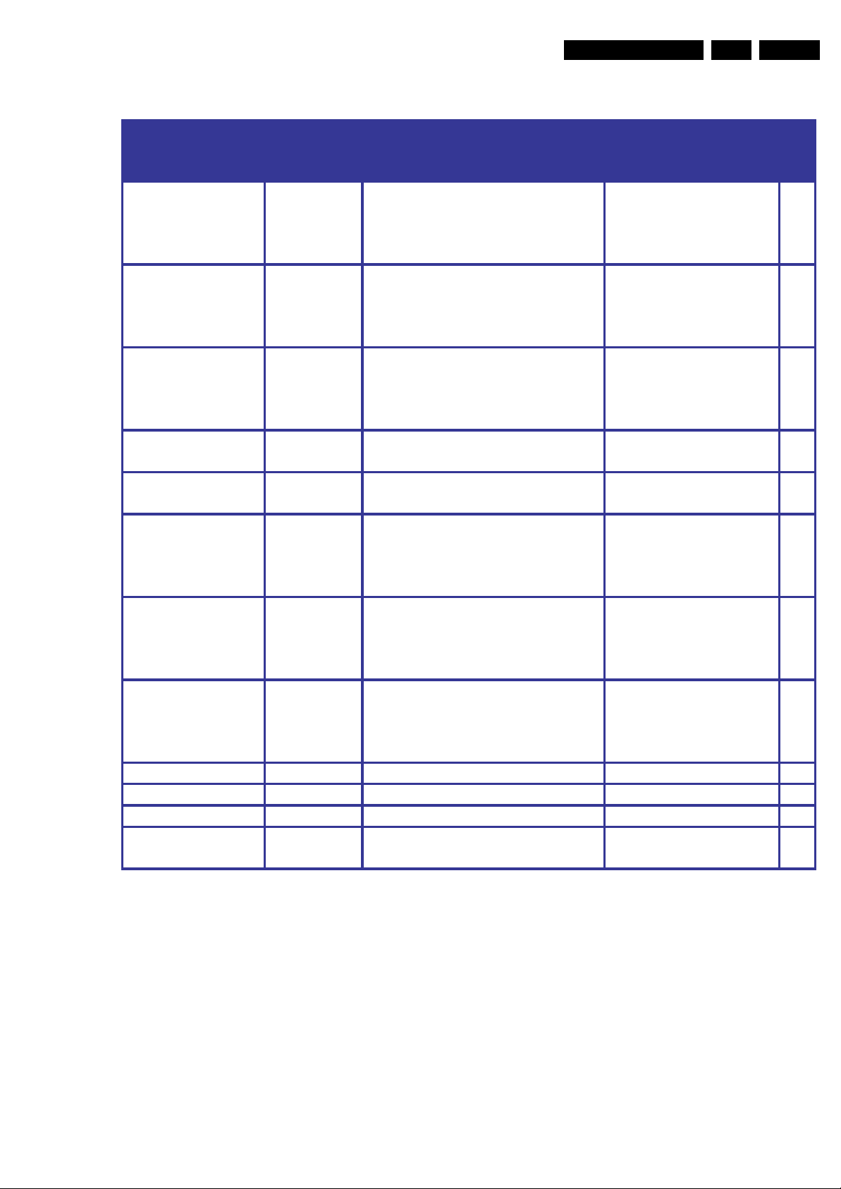
Alignments
EN 17SK7.0L CA 6.
Table 12
OSD
Service setting
Display
String
AGN AGN
Description
Gain for FM demodulator
AGN=0:normal
AGN=1:+6db,
Value
(Min…Max)
/Item list
0:PAL AGN=0,NTSC AGN=0
1:PAL AGN=0,NTSC AGN=1
2:PAL AGN=1,NTSC AGN=0
3:PAL AGN=1,NTSC AGN=1
1
0:normal
AGNE1;AGNE0 AGNE
Extra gain seng for FM
demodulaor
1:+3.8db
2:-6db
1
3:-3db
0:100k
FMWS1;FMWS0 FMWS
Window selecon for FM
demodulator
1:225k
2:450k
1
3:900k
BPB2 BPB2
bypass sound bandpass filter
secon 2
FFI FFI Fast filter IF-PLL
0:acved
1:bypassed
0:Normal
1:increased
1
0
0:off
COR1 COR2 OF AV A-COR COR1 COR2 register seng
1:0-20
2:0-40
1
3:0-100
0:off
COR1 COR2 OF TV T-COR COR1 COR2 register seng
1:0-20
2:0-40
1
3:0-100
0:In AV,FOA=1,FOB=1.In
FOA FOB SETTING FOA-FOB FOA and FOB seng
TV,FOA=0,FOB=0.
1:FOA=0,FOB=1.
0
2:FOA=1,FOB=0
DSG TV-DSG In TV,DSG register 0..1 1
DSG AV-DSG In AV,DSG register 0..1 1
menu le posion MENU-H menu posion adjust 36
DGLS REGISTER
SETTING
DSGLS DSGL Sregister
0:+0db
1:+6db
1
Default
2010-Apr-16
Page 18
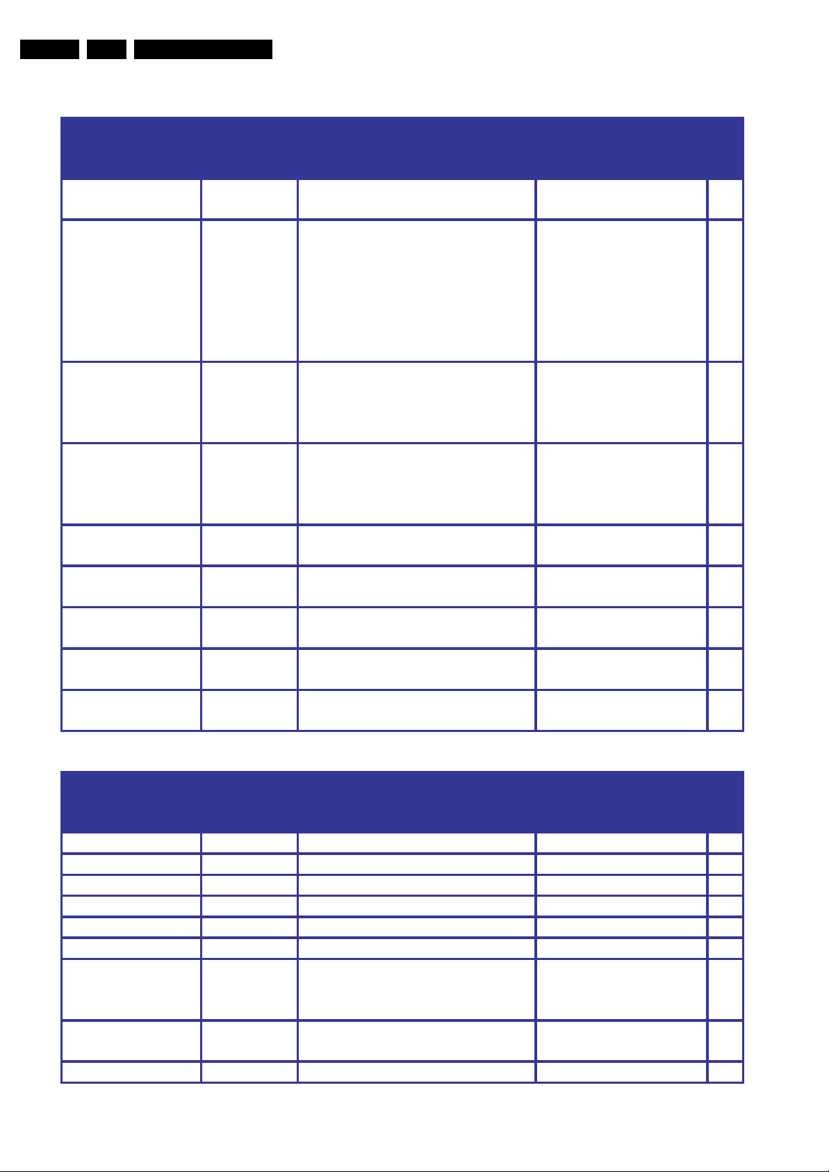
EN 18 SK7.0L CA6.
Alignments
Table 13
OSD
Service setting
Display
Description
String
Slicing level SSL
Slicing level FSL
AAS1;AAS0 AAS
Slicing level horizontal sync
seperator
Force slicing level for vercal
sync
Black area to switch of the black
strenth
SOC0;SOC1 SOC So clipping level
HBL HBL RGB blank mode
WBF WBF Timing of wide blanking
WBR WBR Timing of wide blanking
brightness of black
balance
contrast of black
balance
BT
CT In TV or YUV,Contrast of black balance 0..63 32
In TV or YUV,Brightness of black
balance
Value
(Min…Max)
/Item list
0:50%
1:30%
0
0:dependent
on noise
detector
1:fixed
0
slicing
level of
60%
0:10%
1:12%
2:6%
2
3:8%
0:0%
1:5%
2:10%
2
3:off
0:normal
1:wide
0:3.5us
1:5.9us
0:7.8us
1:10.2us
1
0
8
0..63 32
Default
2010-Apr-16
Table 14
Service setting
OSD
Display
String
Description
Value
(Min…Max)
/Item list
NVM version C0 Char0 48..255
NVM version C1 Char1 48..255
NVM version C2 Char2 48..255
NVM version Y Year 8..10 8
NVM version M Month 0..12 7
NVM version D Day 0..31 8
X-ray protect
XDT XDT
0:Hardware protect.1:Soware
0/1 0
protect
XDT SW ACTIVE XDT-OFFON XDT protect avail
0:Off
1:On
1
SW detect mes XDT-TIME XDT protect detect mes 0..255 10
Default
Page 19
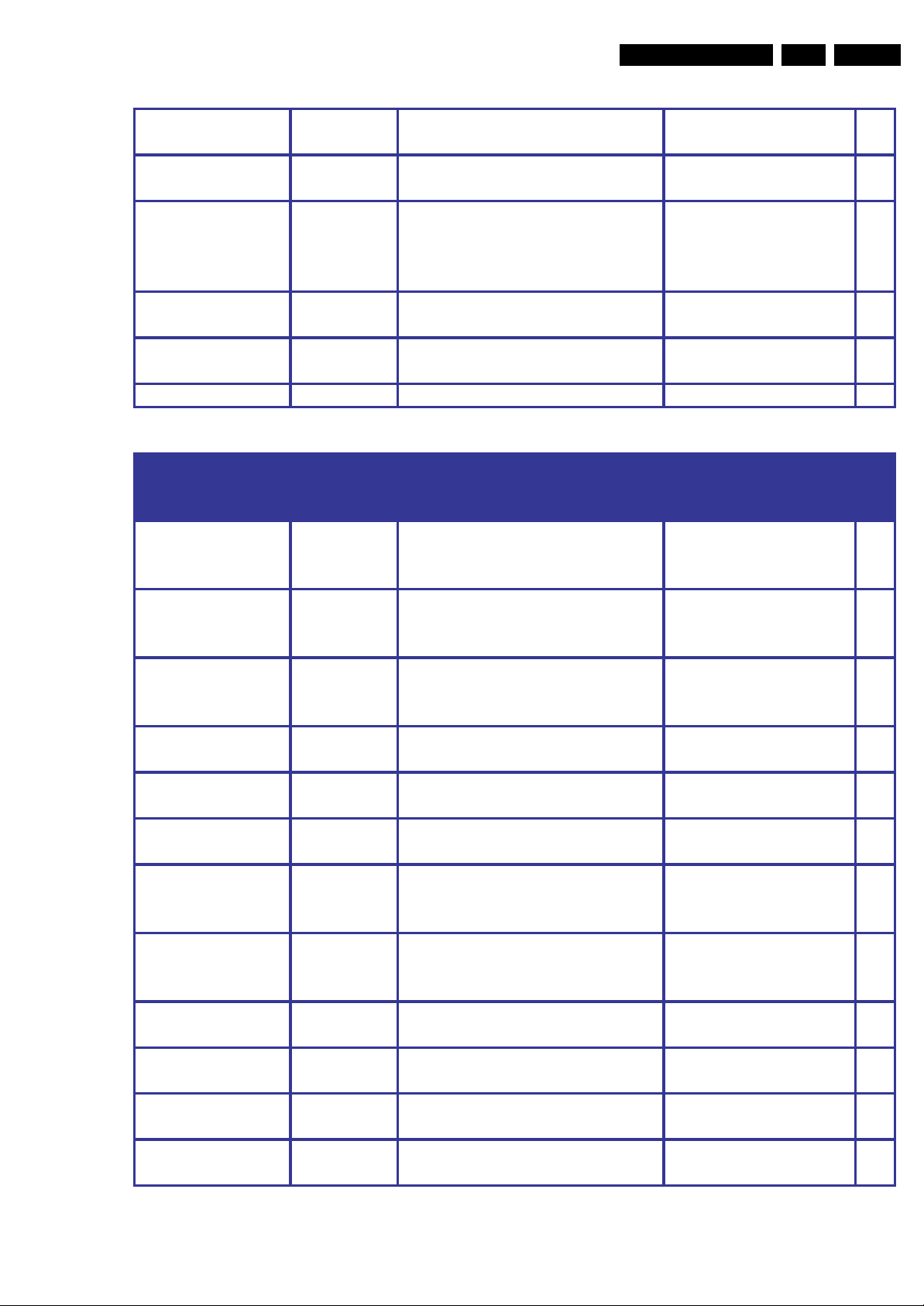
Alignments
EN 19SK7.0L CA 6.
STB SETTING STB In power off,STB register seng
EVG register EVG Field protect funcon
0:STB=0
1:STB=1
0:Off
1:On
0:color sensivity -34dB
CHSE1 CHSE0 register CHSE
If CHSE ON seng on,CHSE value of
strong signal
1:color sensivity -37dB
2:color sensivity -41dB
3:color sensivity -46dB
Auto low signal
idenfy
CHSE ON Auto low signal idenfy
OSD err protect PRO OSD err protect
1:On low signal is -46dB
0:Off
0:Off
1:On
OSD err mes PRO1 OSD err mes 0
Table 15
Service setting
Black level
offset R of YUV
NORMAL
Black level
offset G of YUV
NORMAL
Black level
offset B of YUV
NORMAL
White point R of YUV
NORMAL
White point G of YUV
NORMAL
White point B of YUV
NORMAL
Black level
offset R of YUV
NORMAL
OSD
Display
Description
String
Y-BR
Y-BG
Y-BB
Black level
offset R of YUV NORMAL
Black level
offset G of YUV NORMAL
Black level
offset B of YUV NORMAL
Y-WR White point R of YUV NORMAL -32..+31 0
Y-WG White point G of YUV NORMAL -32..+31 0
Y-WB White point B of YUV NORMAL -32..+31 0
Y-C-BR
Black level
offset R of YUV NORMAL
Value
(Min…Max)
/Item list
-32..+31
-32..+31 0
-32..+31 0
-32..+31 0
1
0
0
0
0
Default
0
Black level
offset G of YUV COOL
Black level
offset B of YUV COOL
White point R of YUV
COOL
White point G of YUV
COOL
White point B of YUV
COOL
Y-C-BG
Y-C-BB
Black level
offset G of YUV COOL
Black level
offset B of YUV COOL
-32..+31 0
-32..+31 0
Y-C-WR White point R of YUV COOL -32..+31 0
Y-C-WG White point G of YUV COOL -32..+31 0
Y-C-WB White point B of YUV COOL -32..+31 0
2010-Apr-16
Page 20
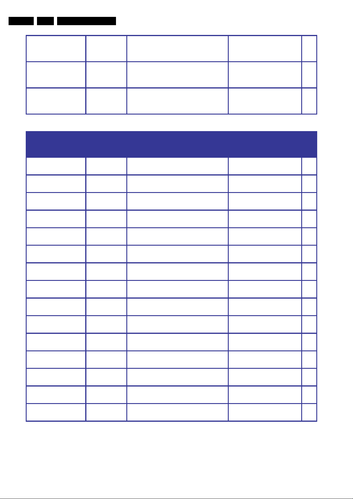
EN 20 SK7.0L CA6.
Alignments
Black level
offset R of YUV
WARM
Black level
offset G of YUV
WARM
Black level
offset B of YUV
WARM
Table 16
Service setting
White point R of YUV
WARM
White point G of YUV
WARM
White point B of YUV
WARM
Black level
offset R of TV COOL
Black level
offset G of TV COOL
Black level
offset B of TV COOL
White point R of TV
COOL
White point G of TV
COOL
White point B of TV
COOL
Black level
offset R of TV WARM
Black level
offset G of TV WARM
Black level
offset B of TV WARM
White point R of TV
WARM
White point G of TV
WARM
White point B of TV
WARM
Y-W-BR
Y-W-BG
Y-W-BB
OSD
Display
String
Black level
offset R of YUV WARM
Black level
offset G of YUV WARM
Black level
offset B of YUV WARM
Description
-32..+31 0
-32..+31 0
-32..+31 0
Value
(Min…Max)
/Item list
Y-W-WR White point R of YUV WARM -32..+31
Y-W-WG White point G of YUV WARM -32..+31
Y-W-WB White point B of YUV WARM -32..+31
T-C-BR
T-C-BG
T-C-BB
Black level
offset R of TV COOL
Black level
offset G of TV COOL
Black level
offset B of TV COOL
-32..+31
-32..+31
-32..+31
T-C-WR White point R of TV COOL -32..+31
T-C-WG White point G of TV COOL -32..+31
T-C-WB White point B of TV COOL -32..+31
T-W-BR
T-W-BG
T-W-BB
Black level
offset R of TV WARM
Black level
offset G of TV WARM
Black level
offset B of TV WARM
-32..+31
-32..+31
-32..+31
T-W-WR White point R of TV WARM -32..+31
T-W-WG White point G of TV WARM -32..+31
T-W-WB White point B of TV WARM -32..+31
Default
2010-Apr-16
Page 21

7. Circuit Descriptions
Circuit Descriptions
EN 21SK7.0L CA 7.
Index of this chapter:
7.1 Introduction
7.2 The various circuits
7.1 Introduction
The SK7.0L CA is a CRT TV based on the 3P67SN platform. In
this chapter, only a general description of the various circuits is
given. For more detailed information, see the circuit diagrams
in this manual.
7.2 The various circuits
7.2.1 Tuner
The function of the tuner is to select the channel to be received
and suppress the interference of neighboring channels, to
amplify the high frequency signal, to improve the receiving
sensitivity and SNR, and to generate a PIF signal through
frequency conversion.
7.2.2 IF Channel
The IF Channel mainly ensures the sensitivity and selectivity of
the complete TV set. The IF AMP integrated in the UOCIII is
made up of a three-stage dual-differential amplifier with a gain
value above 70 dB, a SNR of 55 dB and a bandwidth of 7 MHz.
The video demodulation circuit is made from the built-in PLL
Sync Detector. The spectrum of the demodulation carrier is
unitary and it is not affected by the content of the video signal.
The tuner features stable receptivity while the signal output
from the video detector features high fidelity. The built-in PLL
circuit of the UOCIII generates a 38.0 MHz or 38.9 MHz
demodulation reference signal for the sync detector to
demodulate the video signal; this is called “PLL sync
demodulation”.
7.2.3 Sound Channel
An external ceramic filter is used to select the second SIF
signal for the sound channel of UOCIII from the signal output of
the video detector. The audio signal is obtained after limiting
amplification and demodulation by the intermediate frequency
detector for the SIF signal, and then the audio signal is fed to
the BTSC stereo/SAP decoder TDA9850. From that it is output
to the audio amplifier TFA9842, which drives the speakers to
provide the sound. The intermediate frequency detector and
volume-control attenuator that are built in the UOCIII are set
and adjusted via the CPU.
7.2.6 BTSC stereo/SAP decoder
Input Level Adjustment
The composite input signal is fed to the input level adjustment
stage. The control range is from -3.5 to +4.0 dB in steps of
0.5 dB. The maximum input signal voltage is 2 V (RMS).
Stereo Decoder
The output signal of the level adjustment stage is coupled to a
low-pass filter which suppresses the baseband noise above
125 kHz. The composite signal is then fed into a pilot detector/
pilot cancellation circuit and into the MPX demodulator. The
main L + R signal passes a 75 ms fixed de-emphasis filter and
is fed into the dematrix circuit. The decoded sub-signal L - R is
sent to the stereo/SAP switch. To generate the pilot signal the
stereo demodulator uses a PLL circuit including a ceramic
resonator. The stereo channel separation is adjusted by an
automatic procedure to be performed during set production.
The stereo identification can be read by the I
different pilot thresholds (data STS = 1; STS = 0) can be
selected via the I
SAP Demodulator
The composite signal is fed from the output of the input level
adjustment stage to the SAP demodulator circuit through a 5fH
band-pass filter. The demodulator level is automatically
controlled. The SAP demodulator includes an internal field
strength detector that mutes the SAP output in the event of
insufficient signal conditions. The SAP identification signal can
be read by the I
Noise Detector
The composite input noise increases with decreasing antenna
signal. This makes it necessary to switch stereo or SAP off at
certain thresholds. These thresholds can be set via the I
bus. With ST0 to ST3 the stereo threshold can be selected and
with SP0 to SP3 the SAP threshold. A hysteresis can be
achieved via software by making the threshold dependent of
the identification bits STP and SAPP.
Mode Selection
The stereo/SAP switch feeds either the L - R signal or the SAP
demodulator output signal via the internal dbx noise reduction
circuit to the dematrix/switching circuit. Different switch modes
provided at the output pins OUTR and OUTL are available.
dbx Decoder
The dbx circuit includes all blocks required for the noise
reduction system in accordance with the BTSC system
specification. The output signal is fed through a 73 ms fixed deemphasis circuit to the dematrix block.
2
C-bus.
2
C-bus.
2
C-bus. Two
2
C-
7.2.4 CRT Drive Circuit
In the driver circuit, both the voltage and current of the R/G/B
signal are amplified, after which the CRT drive circuit
modulates the cathode beam current of the CRT. The R/G/B
signal input into the driver circuit is of negative polarity.
7.2.5 Power Supply Circuit
The function of the power supply circuit is to supply various
stabilized operating voltages and to provide protections against
excessive voltages and currents.
SAP Output
Independent of the stereo/SAP switch, the SAP signal is also
available at pin SAP. At SAP, the SAP signal is not dbx
decoded. The capacitor at SDE provides a recommended deemphasis (150 ms) at SAP.
Integrated Filters
The filter functions necessary for stereo and SAP demodulation
and part of the dbx filter circuits are provided on-chip using
transconductor circuits. The required filter accuracy is attained
by an automatic filter alignment circuit.
2010-Apr-16
Page 22
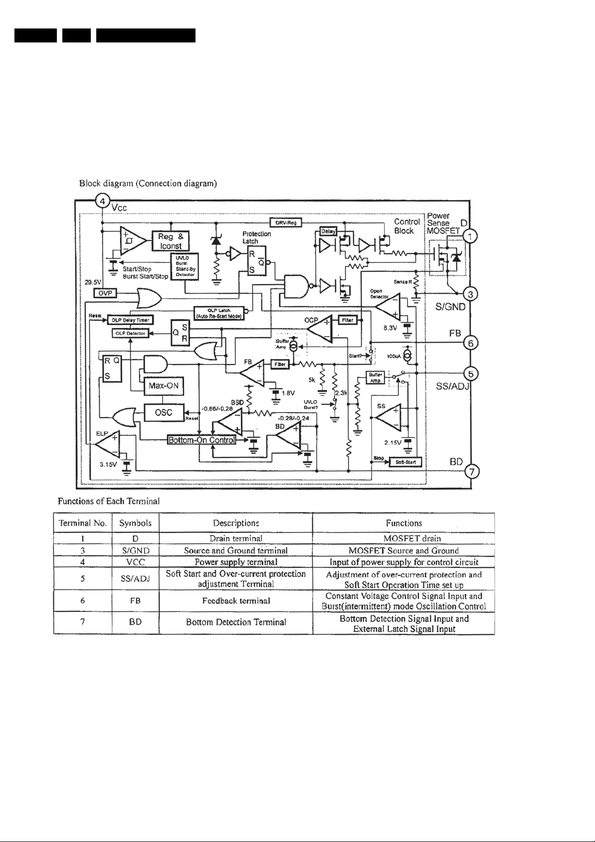
EN 22 SK7.0L CA8.
8. IC Data Sheets
This section shows the internal block diagrams and pin layouts
of ICs that are drawn as “black boxes” in the electrical
diagrams.
8.1 PSU, W6553A, (IC601)
IC Data Sheets
2010-Apr-16
Figure 8-1 Block Diagram and Pin Configuration
H_17210_039.eps
120607
Page 23
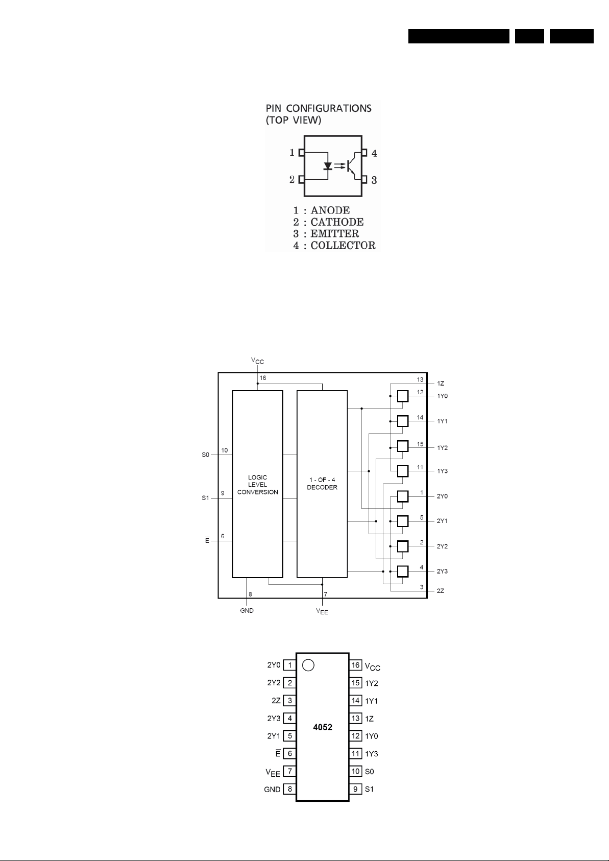
8.2 PSU, IP421, (IC602)
8.3 Input switching, 4052, (IC451)
IC Data Sheets
H_17210_039.eps
120607
Figure 8-2 Block Diagram and Pin Configuration
EN 23SK7.0L CA 8.
Block Diagram
Pin Configuration
Figure 8-3 Block Diagram and Pin Configuration
H_17210_041.eps
120607
2010-Apr-16
Page 24
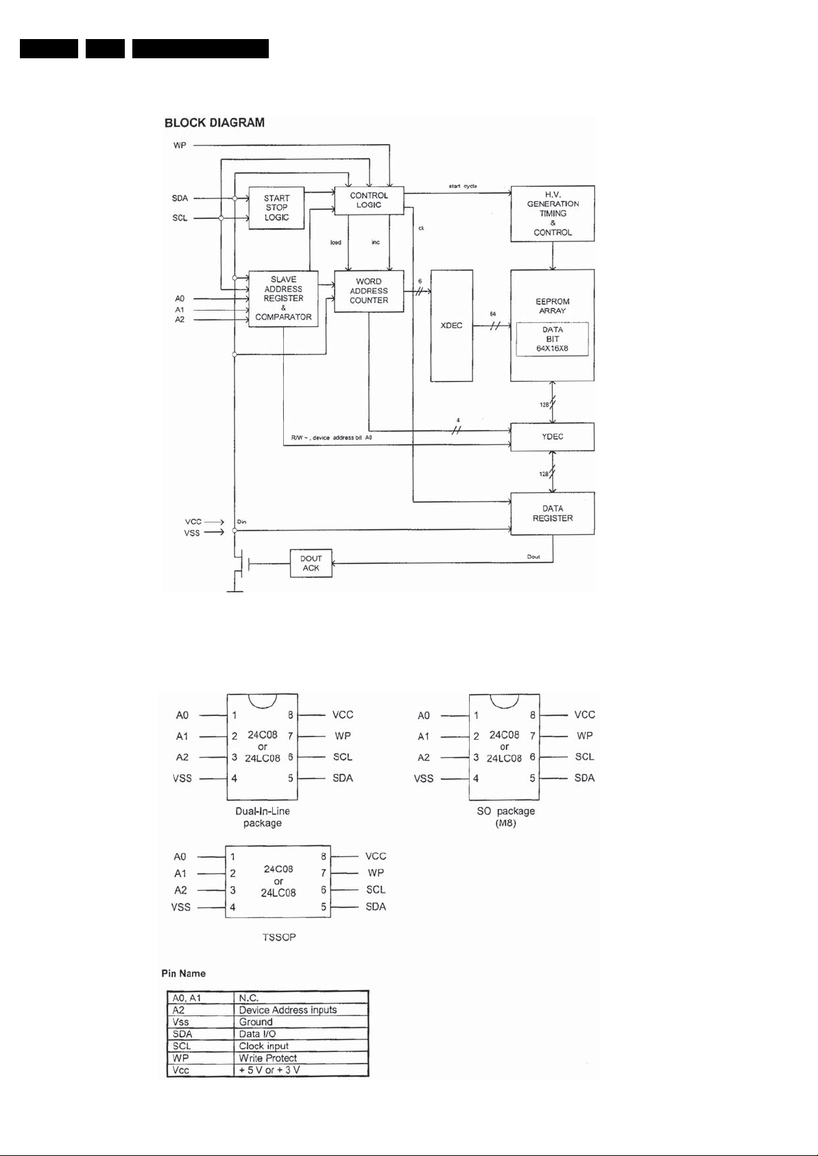
EN 24 SK7.0L CA8.
8.4 Control, 24C08 (IC101)
IC Data Sheets
Pin Configuration
Figure 8-4 Block Diagram
H_17210_035.eps
120607
2010-Apr-16
Figure 8-5 Pin Configuration
H_17210_036.eps
120607
Page 25
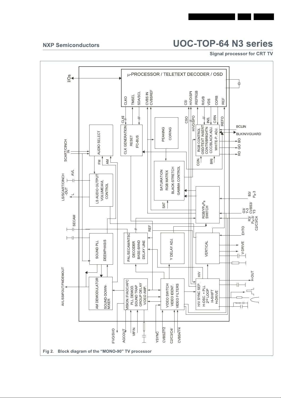
8.5 Control, TDA12165x (IC201)
Pinning
IC Data Sheets
EN 25SK7.0L CA 8.
Figure 8-6 Block Diagram
2010-Apr-16
Page 26
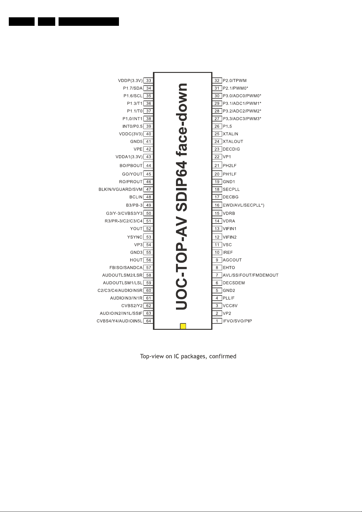
EN 26 SK7.0L CA8.
IC Data Sheets
Pin Configuration
2010-Apr-16
I
Figure 8-9 Pin Configuration
Figure 8-7 Pin Configuration
Page 27
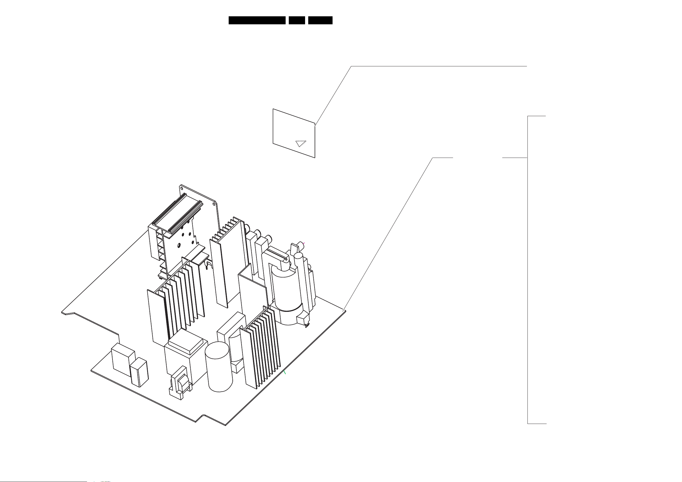
9. Block Diagrams
PWB locations
Block Diagrams
EN 27SK7.0L CA 9.
&57 3$1(/
0$,1
&+$66,6
3$1(/
32:(5 6833/<
/,1( '()/(&7,21
)5$0( '()/(&7,21
781(5 ,)
$9 ,2
2010-Apr-16
$8',2 9,'(2
9,'(2 ,) 6281' ,)
&38 &21752/
$8',2 $03/,),(5
Page 28
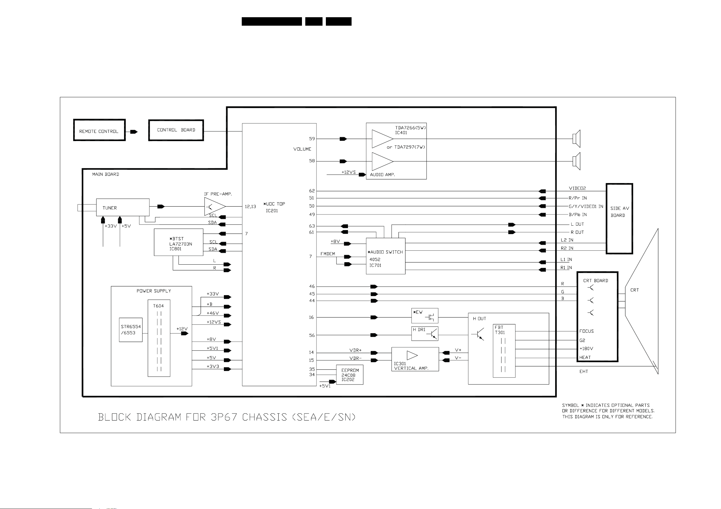
Block Diagram Chassis
Block Diagrams
EN 28SK7.0L CA 9.
2010-Apr-16
Page 29
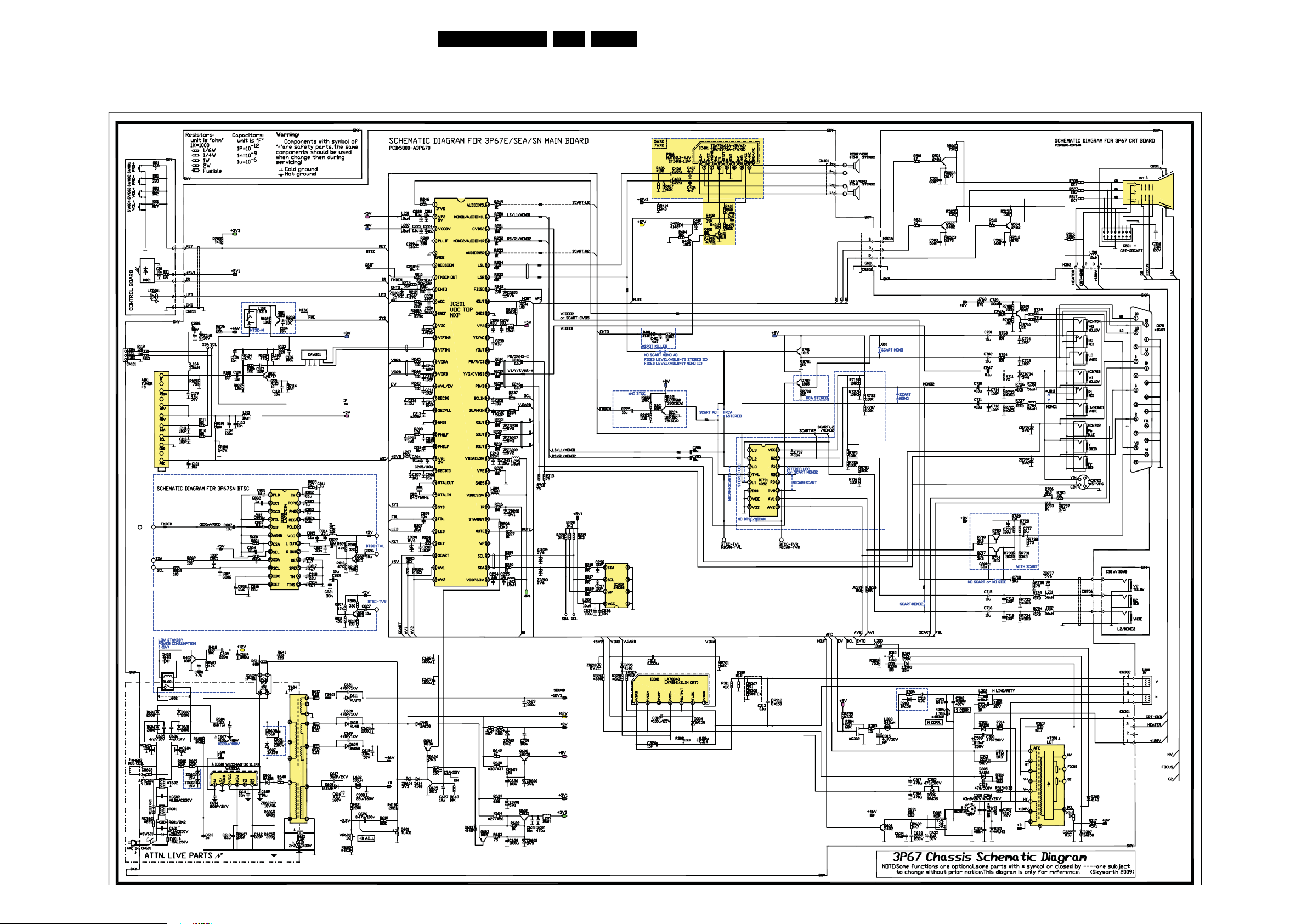
Circuit Diagrams and PWB Layouts
10. Circuit Diagrams and PWB Layouts
21SL7 Schematic Overview Chassis
EN 29SK7.0L CA 10.
2010-Apr-16
Page 30
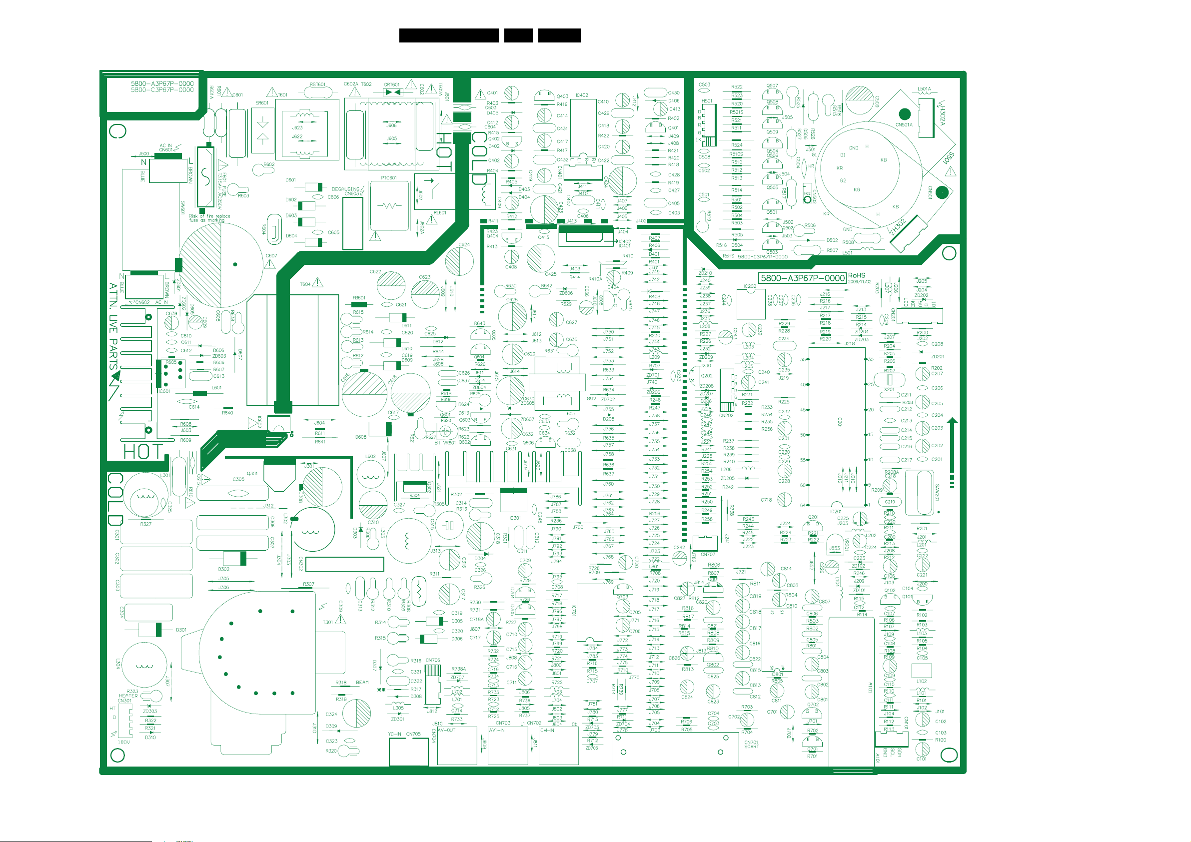
Circuit Diagrams and PWB Layouts
21SL7 Layout Mono Carrier (Top Side)
EN 30SK7.0L CA 10.
2010-Apr-16
Page 31
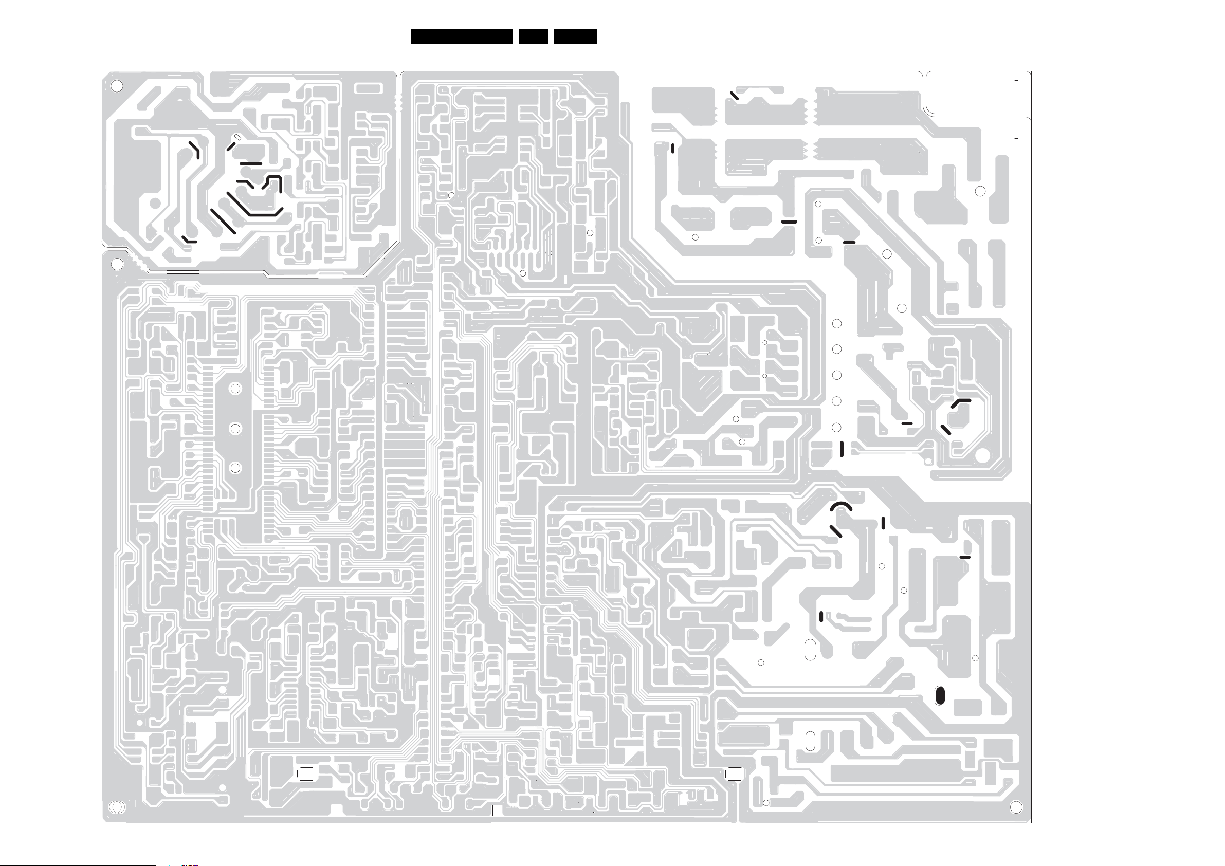
Circuit Diagrams and PWB Layouts
21SL7 Layout Mono Carrier (Bottom Side)
EN 31SK7.0L CA 10.
2010-Apr-16
Page 32
Circuit Diagrams and PWB Layouts
CRT panel
NOT AVAILABLE AT TIME OF PUBLISHING
EN 32SK7.0L CA 10.
2010-Apr-16
10000_043_090121.eps
090121
 Loading...