

Page 1
Si9978DW
Configurable H-Bridge Driver
FEATURES
• H-Bridge or Dual Half-Brid ge Operation
• 20- to 40-V Supply
• Static (dc) Operation
DESCRIPTION
The Si9978DW is an integrated driver for an n-channel
MOSFET H-bridge. The mode control allows operation as
either a full H-bridge driver or as two independent
half-bridges. The DIR/PWM input configuration allows easy
implementation of either sign/magnitude or anti-phase PWM
drive schemes for full H-bridges. Schmitt triggers on the
inputs provide logic signal compatibility and hysteresis for
increased noise immunity. An internal low-voltage regulator
allows the device to be powered directly from a system supply
of 20 to 40 volts. All n-channel gates are driven directly from
low-impedance outputs. The addition of one external
• Cross-Conduction Protected
• Current Limit
• Undervoltage Lockout
• ESD Protected
• Fault Output
capacitor per half -bridge allows in terna l circuitr y to level shift
both the power supply and logic signal for the high-side
n-channel gate drives. Internal charge pumps replace l eak ag e
current lost in the high-side driver cir cuits to provide “stati c”
(dc) operation in any output condition. Protection features
include an undervoltage lockout, cross-conduction prevention
logic, and overcurrent monitors.
The Si9978DW is available in the 24-pin wide-body SOIC
(surface mount) package, specified to operate over the
industrial (-40 to +85°C) temperature range.
Vishay Siliconix
Si9978
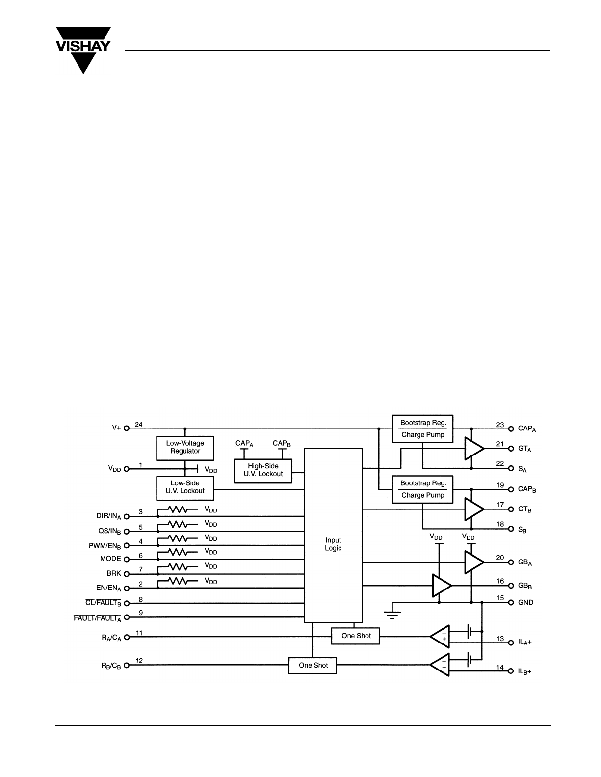
FUNCTIONAL BLOCK DIAGRAM
FaxBack 408-970-5600, request 70011 S-60752—Rev. D, 05-Apr-99
www.siliconix.com 1
Page 2
Si9978DW
Vishay Siliconix
ABSOLUTE MAXIMUM RATINGS
Voltage on pins 2-7 with respect to ground. . . . . . -0.3 to V
DD
+ 0.3 V
Voltage on pin 24 . . . . . . . . . . . . . . . . . . . . . . . . . . . . . . . -0.3 to 50 V
Voltage on pins 17, 19, 21, 23 . . . . . . . . . . . . . . . . . . . . -0.3 to +60 V
Voltage on pins 18, 22 . . . . . . . . . . . . . . . . . . . . . . . . . . . . .-2 to 50 V
Operating Temperature (T
). . . . . . . . . . . . . . . . . . . . . . . - 40 to +85°C
A
Storage Temperature. . . . . . . . . . . . . . . . . . . . . . . . . . . .-65 to 150°C
Maximum Junction Temperature (T
). . . . . . . . . . . . . . . . . . . . . 150°C
J
Power Dissipation . . . . . . . . . . . . . . . . . . . . . . . . . . . . . . . . . 500 mW
RECOMMENDED OPERATING CONDITIONS
V+. . . . . . . . . . . . . . . . . . . . . . . . . . . . . . . . . . . . . . . . . +20 to 40 V
RA, RB. . . . . . . . . . . . . . . . . . . . . . . . . . . . . . . . . . . . . . . . . . . .100 k
DC
Ω
SPECIFICATIONS
Test Conditions
Parameter Symbol
Unless Otherwise Specified
V+ = 20 to 40 V
a
Power
Supply Voltage Range V+ 20 40
Logic Voltage V
DD
Supply Current I+ I
= 0 mA 3 5 mA
DD
14.5 16 17.5
Inputs (DIR, PWM, EN, QS, MODE, BRK)
High-State V
Low-State V
High-State Input Current I
Low-State Input Current I
IH
IL
IH
IL
VIH = V
DD
VIL = 0 V -100 -50 -25
4.0
Outputs
Low-Side Gate Drive, High State V
Low-Side Gate Drive, Low State V
High-Side Gate Drive, High State V
High-Side Gate Drive, Low State V
Capacitor Voltage
c
Low-Side Switching, Rise Time t
Low-Side Switching, Fall Time t
High-Side Switching, Rise Time t
High-Side Switching, Fall Time t
V
GBH
GBL
GTH
GTL
CAP
rL
fL
rH
fH
S
= 0 V
A, B
V+ = 40 V 55
Rise Time = 1 to 10 V
Fall Time = 10 to 1 V
= 600 pF
C
L
Break-Before-Make Time 250
, CL V
FAULT
, CL Leakage Current I
FAULT
OL
OH
IOL = 1 mA 0.4 V
FAULT, CL = V
DD
14 16 17.5
14 16 18
Protection
Low-Side Undervoltage Lockout UVLL 0.8 V
H
High-Side Undervoltage Lockout UVLH S
= 0 V VDD-3.3 V
A, B
Limits
-40 to 85°C
b
Typ
110
50
110
50
0.2 10 µA
DD
0.8
Max
1.0
10
1
1
a
UnitMin
V
V
µA
V
ns
VLow-Side Hysteresis V
S-60752—Rev. D, 05-Apr-99 FaxBack 408-970-5600, request 70011
2 www.siliconix.com
Page 3

Si9978DW
Vishay Siliconix
SPECIFICATIONS
Test Conditi ons
Parameter Symbol
Unless Otherwise Specified
V+ = 20 to 40 V
a
Current Limit
Comparator Input Bias Current I
Comparator Threshold Voltage V
One Shot Pulse Width t
Propagation Delay t
IB
TH
pd
TA = 25°C 90 100 110
RA, RB = 100 kΩ, CA, CB = 100 pF 8 10 12
p
, RB = 100 kΩ, CA, CB = 0.001 µF 80 100 120
R
A
CL = 600 pF 600 ns
Notes:
a. The algebraic convention whereby the most negative value is a minimum and the most positive a maximum, is used in this data sheet.
b. Typical values are for DESIGN AID ONLY, not guaranteed nor subject to production testing.
= (V+) + (VDD)
c. V
CAP
-5 -0.2 5 µA
85 115
Limits
-40 to 85°C
b
Typ
Max
a
TRUTH TABLE
UnitMin
mV
µs
H-BRIDGE MODEL
MODE
IN
PWM/
EN
IN
A
A
EN
B
BRK ILA+ILB+GTAGBAGTBGB
B
CL/
FAULT
B
FAULT/
A
Condition
FAULT
B
DIR/
EN/
QS/
1111 0LXHLL 1 1
1110 0LX LL 1 1
1011 0LXL HL 1 1
Normal
Operation
1010 0LXL L 1 1
1 X 1 X X 1 L X L H K H 1 1 Brake
1 X0X X X L X LLLL 1 1 Disable
1 X 1 X X 0 X L L L L Overcurrent
1 XXX X X X X LLLL 1 0
Undervoltage
on V
DD
HALF-BRIDGE MODEL
DIR/
EN/
QS/
MODE
IN
EN
IN
A
A
EN
B
BRK ILA+ILB+GTAGBAGTBGB
B
011X0XLLHLLL 1 1
0 0 1X 0 X L L LHLL 1 1
0 X 01 1 X L L LLHL 1 1
0 X00 1 X L L LLLH 1 1
0X1XXX XLLXX 1
0XXX1XX XXLL 1
0 XXX X X X X LLLL 0 0
PWM/
CL/
FAULT
B
FAULT/
A
Condition
FAULT
B
Normal
Operation
Overcurrent on
A
Overcurrent on
B
Undervoltage
on V
DD
FaxBack 408-970-5600, request 70011 S-60752—Rev. D, 05-Apr-99
www.siliconix.com 3
Page 4

Si9978DW
Vishay Siliconix
PIN CONFIGURATION
PIN DESCRIPTION
Pin 1: V
VDD is an internally generated voltage. It is connected to this
pin to allow connection of a decoupling capacitor. A minimum
of 1 µF is recommended.
Pin 2: EN/EN
The EN input allows normal operation when at logic “1”, and
turns all gate drive outputs off when at logic “0”. When the
mode pin is at logic “1”, EN controls the entire H-bridge. When
the mode pin is at logic “0”, this pin becomes the ENABLE pin
for half-bridge A.
Pin 3: DIR/IN
The function of this pin is determined by the MODE pin.
When the MODE pin is at logic “1”, it is the DIR pin, and when
MODE is at logic “0”, it is the IN
As the DIR inpu t, it is the directio n control for the H-br idge,
and determines which diagonal pair of power MOSFETs is
active. A l ogic “1” turns on GT
“0” turns on GT
anti-phase PWM control, the DIR input serves as the PWM
input.
As the IN
When at logic “1”, the high-side MOSFET is turned on, and
when at logic “0”, the low-side MOSFET is turned on.
Pin 4: PWM/EN
With the mode pin at logic “1”, this pin is the PWM input. It
controls the switching of the active diagonal pair. A logic “1”
DD
A
A
pin.
A
and enables G BB, while a logic
and enables GBA. When implem enting an
B
pin, it is the input that controls the “A” half-bridge.
A
B
A
turns the active MOSFETs on, w hile a l ogic “0” turns it off . The
QS input determines whether the bottom or both bottom and
top MOSFETs are switched. When implementing an
anti-phase PWM control, the PWM input is connected to a
logic “1”. Wh en the mode pin is at l ogic “0 ”, this pin beco mes
the ENABLE pin for half-bridge B.
Pin 5: QS/IN
With the mode pin at logic “1”, this input determines whether
the bottom MOSFETs of the H-bridge or both bottom and top
MOSFETs switch in response to the PWM signal. A logic “1”
on this input enables only the bottom MOSFETs. This is the
default condi tion as thi s pin is pu lled up i nter nally. When this
pin is pulled to grou nd, bot h th e bottom an d top M OSFETs are
enabled.
This input controls the B half-bridge when the MODE pin is at
logic “0”. When at logic “1”, the high-side MOSFET is turned
on, and when at logic “0”, the low-side MOSFET is turned on.
Pin 6: MODE
This input determines whether the Si9978 functions as an
H-bridge or as two independent half-bridges. When the
MODE pin is at logic “1”, the Si9978 functions as an H-bridge,
and when MODE is at logic “0”, it functions as two
independent half-bridges.
Pin 7: BRK
When this input and MODE are at logic “1”, both bottom gate
drives are switched high, turning on the bottom MOSFETs.
When this input is at logic “0”, the Si9978 operates normally.
B
S-60752—Rev. D, 05-Apr-99 FaxBack 408-970-5600, request 70011
4 www.siliconix.com
Page 5

Si9978DW
Pin 8: CL/FAULT
B
This is an open drain output which is active low. When the
MODE pin is at logic “1”, this pin functions as CL
and
indicates that the H-bridge is in current limit. It stays low for
the duration of the current limit one-shot. With the MODE pin
at logic “0”, it serves as the FAULT
output for half-bridge B to
indicate when an undervoltage or overcurrent condition is
detected. When ind icatin g an o v e rcurrent co nditio n, the output
stays low for the duration of the current limit one-shot. The
output resets automatically when the condition clears.
FAU LT
Pin 9: FAULT
/FAULT
A
This is an open drain output which is switched low when an
undervoltage or overcurrent condition is detected. When
indicating an overcurrent condition, the output stays low for
the duration of the current limit one-shot. When the MODE
pin is at logic “1”, this pin is the H-bridge FAULT
the MODE pin at logic “0”, it ser ves as the FAULT
half-bridge A. The FAULT
output resets automatically when
output. With
output for
the condition clears.
Pin 10: NC
No internal connection.
Vishay Siliconix
comparators. Externally they are connected to the source(s)
of the low-side MOSFET(s) and the current sense resistor.
Pin 15: GND
The GND pin is the ground return for V+ and the ground
reference for the logic. Also, this is the ground reference input
for the current limit comparators and is connected to the
ground side of the internal 100-mV references. This pin
should be connected directly to the ground side of the current
sensing resistors.
Pin 16: GB
and Pin 20, GB
B
A
These pins drive the gates of the low-side power MOSFETs.
Pin 17: GTB and Pin 21, GT
A
These pins drive the gates of the high-side power MOSFETs.
Pin 18: S
and Pin 22, S
B
A
These are the source connections of the high-side power
MOSFETs, the drain of the external low-side power MOSFET,
the negative terminal of the bootstrap capacitor, and the
output for each half-bridge.
Pin 11: RA/CA
The timing resistor and capacitor for the current limit one-shot
are connected to this pin. The values of the resistor and
capacitor determine the off time set by the one-shot. The
one-shot is triggered when the current limit comparator
detects an overcurrent condition.
Pin 12: R
B/CB
The timing resistor and capacitor for the current limit one-shot
are connected to this pin. The values of the resistor and
capacitor determine the off time set by the one-shot. The
one-shot is triggered when the current limit comparator
detects an overcurrent condition.
Pin 13: IL
+ and Pin 14, ILB+
A
These are the overcurrent sense i nputs. Internally, they are
connected to the noninverting inputs of the current limit
Pin 19: CAP
and Pin 23, CAP
B
A
These are the connections for the positive terminals of the
bootstrap ca pacitors C
and CBB. A 0.01-µF capacitor can
BA
be used for most applications.
Pin 24: V+
This is the only external power supply required for the
Si9978DW, and must be the same supply used to power the
H-bridge it is driving. The Si9978DW powers the low-voltage
logic, low-side gate driver, and bootstrap/ charge pump
circuits from self-contained voltage regulators which require
only a bootstrap capacitor on the CAP pins.
No voltage sensing circuitry monitors V+ directly; however, the
low-voltage, internally generated supply and the bootstrap
voltage (which are derived from V+) are directly protected by
undervoltage monitors.
FaxBack 408-970-5600, request 70011 S-60752—Rev. D, 05-Apr-99
www.siliconix.com 5
Page 6

Si9978DW
Vishay Siliconix
APPLICATIONS
FIGURE 1. Basic H-Bridge Circuit
S-60752—Rev. D, 05-Apr-99 FaxBack 408-970-5600, request 70011
6 www.siliconix.com
 Loading...