

Page 1

12-V Voice Coil Motor Driver
FEATURES
D 1.8-A H-Bridge Output
D Class B Linear Operation
D Externally Programmable Gain and
Bandwidth
DESCRIPTION
The Si9961 is a linear actuator (voice coil motor) driver suitable
for use in disk drive head positioning systems. The Si9961
contains all of the power and control circuitry necessary to
drive the VCM that is typically found in 3
drives and optical disk drives. The driver is capable of
delivering 1.8 A at a nominal supply of 12 V.
The Si9961 provides all necessary functions including a motor
current sense amplifier, a loop compensation amplifier and a
power amplifier featuring four complementary MOSFETs in a
H-bridge configuration. The output crossover protection
ensures no cross-conducting current and true Class B
D Undervoltage Head Retract
D Programmable Retract Current
D Low Standby Current
1
/2-inch hard disk
Si9961
Vishay Siliconix
D Rail-to-Rail Output Swing
D Single 12-V Supply
D System Voltage Monitor with Fault Output
operation during linear tracking. Externally programmable
gain switch at the input summing junction increases the
resolution and dynamic range for a given DAC. The head
retract circuitry can be activated by either an undervoltage
condition or an external command. An external resistor is
required to set the VCM current during retract.
The Si9961 is constructed on a self-isolated BiC/DMOS power
IC process. The IC is available in 24-pin SO package for
operation over the commercial, C suffix (0 to 70_C)
temperature range.
FUNCTIONAL BLOCK DIAGRAM
V
CC
IA2–
I
RET
OA2
4
5
23
V
R
9
6
11
22
10
A2
–
+
Acceleration Error
V
FAULT
RETRACT
Enable
GAIN
SELECT
R
EXT
V
REFVREF–
V
8 R
+
–
Retract
Control
–
+
7 R
A3
R
A4
A5
–
+
V+
818712
Voltage
Monitor
R
V
R
R
Q1
Q2
V
DD
Q3
17
OUTPUT
A
OUTPUT
19
Q4
B
Document Number: 70014
S-20883—Rev. G, 24-Jun-02
R
INHRINL
20161415211332421
I
R
FB
SENSE
OUT
I
SENSE
IN+
I
SENSE
IN–
GND
SA SB
www.vishay.com
1
Page 2
Si9961
Vishay Siliconix
ABSOLUTE MAXIMUM RATINGS
Voltages Referenced to Common Pin
V+ Supply Range –0.3 V to 16 V. . . . . . . . . . . . . . . . . . . . . . . . . . . . . . . . . . . .
Pin (FAULT
) –0.3 V to VCC + 0.3 V. . . . . . . . . . . . . . . . . . . . . . . . . . . . . . . . . .
Pin (Output A & B, Source A & B) –0.3 V to V
Pin (All Others) –0.3 V to V+ + 0.3 V. . . . . . . . . . . . . . . . . . . . . . . . . . . . . . . .
Maximum Clamp Current
Output A, Output B (Pulsed 10 ms at 10% duty cycle) "1.8 A. . . . . . . . . . . .
Pin (All Others) "20 mA. . . . . . . . . . . . . . . . . . . . . . . . . . . . . . . . . . . . . . . . . .
Storage Temperature –65 to 150_C. . . . . . . . . . . . . . . . . . . . . . . . . . . . . . . . .
DD
+ 0.3 V. . . . . . . . . . . . . . . .
Operating Temperature 0 to 70_C. . . . . . . . . . . . . . . . . . . . . . . . . . . . . . . . . . .
Junction Temperature (T
Power Dissipation (Package)
24-Pin SOIC
b
Thermal Impedance (
24-Pin SOIC 40_C/W. . . . . . . . . . . . . . . . . . . . . . . . . . . . . . . . . . . . . . . . . . . . . .
Notes
a. Device mounted with all leads soldered or welded to PC board.
b. Derate 25 mW/_C above 25_C.
) 150_C. . . . . . . . . . . . . . . . . . . . . . . . . . . . . . . . . . . .
J
a
a
)
JA
3.125 W. . . . . . . . . . . . . . . . . . . . . . . . . . . . . . . . . . . . . . . . . . . .
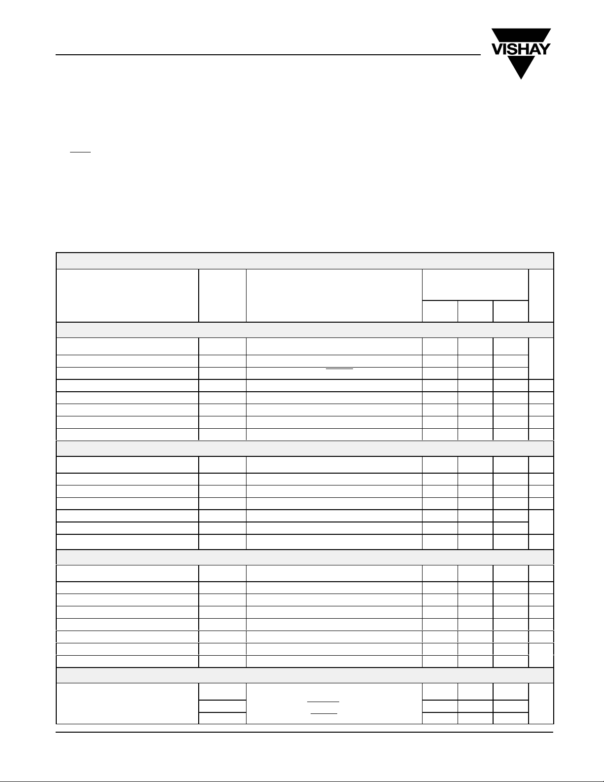
SPECIFICATIONS
T est Conditions
Unless Otherwise Specified
V+ = 12 V "10%, VDD = 11.6 V "10%
V
Parameter Symbol
= 5 V "10%, V
CC
V
REF
= GND = 0 V
REF–
= 5 V "5%
Min
Bridge Outputs (A4, A5)
High Level Output Voltage V
Low Level Output Voltage V
Clamp Diode Voltage V
OH
OL
CL
Amplifier Gain Output V
Dynamic Crossover Current Measured at V
Slew Rate SR 1 V/S
Small Signal Bandwidth (–3 dB) 0.2 MHz
Input Deadband –60 60 mV
IOH = 1.0 A, VDD = 10.2 V, OA2= V
IOL = –1.0 A, OA2 = V
REF
"1 V 8.0 9.1
REF
"1 V 0.6 1.1
IF = 1.0 A, ENABLE = High 2.5
= V
RANGE
"2 V 12 16 18 V/V
REF
DD
A2, Loop Compensation Amplifier
Input Offset Voltage V
Input Bias Current I
Unity Gain Bandwidth R
Slew Rate SR 1 V/s
Power Supply Rejection Ratio PSRR @ 10 kHz 50
Open Loop Voltage Gain A
Output Voltage Swing V
OS
B
VOL
Gain Select = High, IA
= 10 k, C
LOAD
O
R
LOAD
LOAD
= 10 k to V
–
= 5 V –50 50 nA
2
= 100 pF to V
REF
REF
V
REF
A3, Current Sense Amplifier
Input Offset Voltage V
Input Impedance R
Small Signal Bandwidth (–3 dB) R
Common Mode Rejection Ratio CMRR @ 5 kHz 50 dB
Slew Rate SR 2 V/s
Gain 3.9 4 4.1 V/V
Input Common-Mode Voltage Range V
Output Voltage Swing V
OS
CM
I
IN
LOAD
IN+ to I
SENSE
= 10 k, C
LOAD
IN– 5 k
SENSE
= 100 pF to V
REF
T o GND –0.3 2
R
O
LOAD
= 10 k, C
= 100 pF to V
LOAD
REF
V
REF
Supply
I
CC Static, No Load
Supply Current (Normal)
I
V+
I
DD
RETRACT = High 2 5
ENABLE = Low
Limits
C Suffix 0 to 70_C
b
TypaMaxbUnit
10 mA
–8 8 mV
1 MHz
80
–2 V
–5 5 mV
1 MHz
–2 V
5 13
REF
REF
0.01
+2 V
+2
V
dB
V
mA
www.vishay.com
2
Document Number: 70014
S-20883—Rev. G, 24-Jun-02
Page 3

Si9961
Vishay Siliconix
SPECIFICATIONS
T est Conditions
T est Conditions
Unless Otherwise Specified
Unless Otherwise Specified
V+ = 12 V "10%, VDD = 11.6 V "10%
V+ = 12 V "10%, VDD = 11.6 V "10%
V
V
= 5 V "10%, V
= 5 V "10%, V
CC
Parameter UnitMax
Symbol
CC
V
V
REF
REF
= GND = 0 V
= GND = 0 V
REF–
REF–
= 5 V "5%
= 5 V "5%
Min
Supply
I
CC Static, No Load
Supply Current (Standby)
VDD Range V
VCC Range V
V+ Range V+ 10.8 12 13.2
I
V+
I
DD
DD
CC
RETRACT = High 0.2 0.4
ENABLE = High
Normal Mode 10.2 11.6 13.2
Retract Mode 2.0 14
Gain Select Switch
RFB Switch Resistance 108 240
R
Switch Resistance
INH
R
Switch Resistance 810 1800
INL
V
(EXT)
REF
Input Current I
External Voltage Range V
REF
REF
IA2– = 5 V
OA2 = V
REF
Power Supply Monitor
VCC Undervoltage Threshold V
Hysteresis 40 mV
V+ Undervoltage Threshold V
Hysteresis 100 mV
= 5.0 V 3.82 4.12 4.42 V
REF
= 5.0 V 9.1 9.8 10.6 V
REF
Gain Select, RETRACT, ENABLE Input
Input High V oltage V
Input Low Voltage V
Input High Current I
Input Low Current I
IH
IL
IH
IL
VIN = 5 V –1 1
VIN = 0 V –1 1
FAULT Output
Output High Voltage V
Output Low Voltage V
Output High Sourcing Current I
OH
OL
OHS
IOH = –100 A
IOL = 1.6 mA 0.25 0.50
V
= 0 V 400 1100 A
OUT
RETRACT Current Control (RETRACT = Low, Output Current from A to B)
I
Bias Voltage V(I
RET
Retract Output Pull-Up Voltage V
Retract Output Pull-Down Current I
Maximum Emergency Retract Current I
Retract Current VDD Supply Rejection Ratio VDD = 2 V to 14 V, R
Retract Current Temperature Coefficient VDD = 10 V, R
Notes
a. Typical values are for DESIGN AID ONLY, not guaranteed nor subject to production testing.
b. The algebraic convention whereby the most negative value is a minimum and the most positive a maximum.
) VDD = 10 V, R
RET
OUT A
OUTB
(Max) VDD = 2 V, V
OUTB
VDD = 10 V, V
RET
VDD = 2.5 V to 14 V, I
= 5 V R
OUTB
R
= 0.5 , TA = 25_C
SB
= 0.7 V R
OUTB
RET
RET
= 3.74 k 0.66
= 30 mA VDD –1
OUTA
= 3.74 k
RET
= < 10 , RSB = 0.5 , 40
= 3.74 k 3.0 %/V
RET
= 3.74 k –0.3 %/_C
Limits
C Suffix 0 to 70_C
b
4.5 5 5.5
0.15 0.40 0.65 mA
4.75 5 5.25 V
3.5
V
CC
–0.8
22 30 38
a
Typ
0.8 1.6
135 300
V
CC
–0.33
b
0.01
1.5
mA
V
V
A
V
V
mA
mA
Document Number: 70014
S-20883—Rev. G, 24-Jun-02
www.vishay.com
3
Page 4

Si9961
Vishay Siliconix
PIN CONFIGURATION
24-Pin SOIC
(Wide Body)
APPLICATIONS
Introduction
R
1
INH
R
2
INL
OUT OA2
I
SENSE
FAULT
EXT V
RETRACT GND
GAIN SELECT SOURCE A
ENABLE GND
V
3
4
V
5
CC
I
RET
6
7
REF
V+ OUTPUT A
8
9
10
11
12
REF–
Top View
24
23
22
21
20
19
18
17
16
15
14
13
R
FB
IA2–
I
(IN)–
SENSE
SOURCE B
OUTPUT B
(Spindle Supply)
V
DD
I
(IN)
SENSE
User-Programmable Gains
Order Number: Si9961ACY
+
The Si9961 Voice Coil Motor (VCM) driver integrates the active
feedback and drive components of a head-positioning servo
loop for high-performance hard-disk applications. The Si9961
operates from a 12-V ("10%) power supply and delivers 1 A
of steady-state output current. This device is made possible by
a power IC process which combines bipolar, CMOS and
complimentary DMOS technologies. CMOS logic and linear
components minimize power consumption, bipolar front-ends
on critical amplifiers provide necessary accuracy, and
complimentary (p- and n-channel) DMOS devices allow the
transconductance output amplifier to operate from ground to
. Two user-programmable, current feedback/input voltage
V
DD
ratios may be digitally selected to optimize gain for both seek
and track following modes, to maximize system accuracy for
a given DAC resolution. An undervoltage lockout circuit
monitors the V+ supply and generates a fault signal to trigger
an orderly head-retract sequence at a voltage level sufficient
to allow the spindle motor’s back EMF-generated voltage to
supply the necessary head parking energy. Head retract can
also be commanded via a separate RETRACT input. VCM
current during retract can be user programmed with a single
external resistor. External components are limited to R/C filter
components for loop compensation and the resistors that are
required to program gain, retract current, and the load current
sense.
www.vishay.com
4
During linear operation, the transconductance amplifiers’
gains (input voltage at V
by external resistors R
gain input. After selecting a value for R
vs. VCM current, in Figure 1) are set
IN
R5, RSA, and RSB and selected by
3
and RSB that will yield
SA
the desired VCM current level, the High and Low feedback
gain ratios may be determined by the following:
R
1
High Gain +
Low Gain +
5
ǒ
Ǔ
R
3
R
5
ǒ
Ǔ
R
4
Where RS = RSA = R
4R
1
4R
SB
(GAIN SELECT Input = High)
S
(GAIN SELECT Input = Low)
S
Input offset current may then be calculated as:
I
OS
1
+
4R
S
ǒ
ǒ
ǒ
Where RIN = R3 or R
RS) R
4
Ǔ
IN
V
) 5V
Ǔ
OSA2
R
IN
Ǔ
IAS3
Document Number: 70014
S-20883—Rev. G, 24-Jun-02
Page 5

Si9961
Vishay Siliconix
mP
mP
12 V
System
Supply
R
RET
GAIN
SELECT
5 V
5-V Ref
818712
V+
FAULT
4
5
V
CC
23
IA2–
–
C
L
R
L
9
6
11
22
10
+
V
R
RETRACT
I
RET
ENABLE
OA2
R
INHRINL
Voltage
Monitor
A2
Acceleration Error
V
R
EXT
V
REF
8 R
R
+
–
V
R
Retract
Control
–
+
R
7 R
R
I
FB
A3
SENSE
OUT
A4
A5
V
REF–
V
R
–
+
I
I
SENSE
SENSE
IN+
IN–
V
DD
Q1
Q2
GND
AB
Back EMF Supply
Q3
Q4
20161415211332421
17
OUTPUT
A
19
OUTPUT
B
C2
I
OUT
VCM
R2
R3 R4 R5
V
IN
FIGURE 1. Si9961 Typical Application
Head Retract
A low on the RETRACT
input pin turns output devices Q1 and
Q4 on, and output devices Q2 and Q3 off. Maximum VCM
current can be set during head retract by adding an external
resistor between the IRET pin and ground. Maximum retract
current may be calculated as:
I
OUT
+ 175 x I
ret
+ 175 x
0.66 V
R
ret
Head retract can be initiated automatically by an undervoltage
condition (either the 12-V or 5-V supplies on the Si9961) by
connecting the FAULT output to the RETRACT input.
A high ENABLE
high-impedance state. The ENABLE
input puts both driver outputs in a
function can be used to
R
SA
R
SB
eliminate quiescent output current when power is applied but
the head has been parked, such as a sleep mode. A
sleep-mode power down sequence should be preceded by a
retract signal since a power failure during this state may not
provide adequate spindle-motor back EMF to permit head
retraction.
Transconductance Amplifier Compensation
The Si9961CY features an integrated transconductance
amplifier to drive the voice coil motor (VCM). To ensure proper
operation, this amplifier must be compensated specifically for
the VCM being driven. As a first approximation, the torque
constant and inertia of the VCM may be ignored, although they
will have some influence on the final results, especially if large
values are involved. (See Figure 1.)
Document Number: 70014
S-20883—Rev. G, 24-Jun-02
www.vishay.com
5
Page 6

Si9961
Vishay Siliconix
Frequency Compensation:
The VCM transconductance (in siemens) of this simplified
case may be expressed in the s (Laplace) plane as:
1
L
g
v
v
+
s )
R
v
L
v
Where Rv = VCM resistance in ohms
= VCM inductance in henrys
L
V
s is the Laplace operator
In this case, the transconductance pole is at –Rv/Lv. It is
desirable to cancel this pole in the interest of stability. To do
this, a compensation amplifier is cascaded with the VCM and
its driver. The transfer function of this amplifier is:
1
RL C
s
Ǔ
L
Hc+ A
ǒ
s )
Where RL= Compensation amplifier feedback
resistor in ohms
CL= Compensation amplifier feedback
capacitor in farads
A = Compensation amplifier and driver
voltage gain at high frequency
If R
x CL is set equal to Lv/Rv, then the combined open loop
L
transconductance in siemens becomes:
+
A
s L
v
g
to
In this case, the transconductance has a single pole at the
origin. If this open loop transfer is closed with a
transimpedance amplifier having a gain of B ohms, the
resultant closed loop transconducatance stage has the
transfer function (in siemens) of:
A
L
s )
v
A B
L
v
g
+
tc
Where B = Current feedback transimpedence amplifier gain in
ohms.
The entire transconductance now contains only a single pole
at –A*B/Lv. A and B are chosen to be considerably higher than
the servo bandwidth, to avoid undue phase margin reduction.
A = 16 x R
C
=Lv/(Rv x RL) = 100 x 10–6/RL farads
L
/10000
L
Gain Optimization:
There are three things to consider when optimizing the gain (A)
above. The first is servo bandwidth. The main criterion here is
to avoid having the transconductance amplifier cause an
undue loss of phase margin in the overall servo (mechanical
+ electrical + firmware) loop. The second is to avoid confirguing
a bandwidth that is more than required in view of noise and
stability considerations. The third is to keep the voltage output
waveform overshoot to a level that will not cause
cross-conduction of the output FETs.
The first two problems can be considered together. Let us
assume a disk drive with a spindle RPM of 4400 and with
50 servo sectors per track. The sample rate is therefore:
fs + 50
440
60
This is a sample frequency of 3667 Hz
As a rule of thumb, the open loop unity gain crossover
frequency of the entire servo (mechanical + electrical +
firmware) loop should be less than 1/10 of the sample
frequency. In this example, the servo open loop unity gain
crossover frequency would be less than 367 Hz. If we allow
only a 10_ degradation in phase margin due to the
transconductance amplifier, then a phase lag of 10_ at 367 Hz
is acceptable. This results in a 3-dB point in the
transconductance at :
+
367
tan(10
)
f
3db
or a 3-dB point in the transconductance at 2081 Hz.
The pole in the closed loop transconductance (–A * B / Lv)
should then be 2081 * 2 * = 13075. This means that A = 9.8.
From the above equation for A, RL = 6.2 k. This sets the
minimum gain limit governed by the servo bandwidth
requirements. The gain should not be much greater than this,
since increased noise will degrade the servo response.
The third problem, keeping the transconductance amplifier
voltage output wave form overshoot to a level that will not
cause the wrong output FETs to conduct, can be evaluated by
deriving the voltage transfer function of the closed loop
transconductance amplifier from input voltage to output
voltage (Vin to output A and B on the reference schematic).
As a typical example, in the referenced schematic, assume
that Rsa and Rsb = 0.5 , R5= R3 = 10 k, VCM inductance
(Lv) = 1.5 mH, VCM resistance (Rv) = 15 . Hence:
= 15
R
v
= 1.5 mH
L
v
B=2
www.vishay.com
6
This is :
Hto+ A
s ) p
s ) x
Where p = 1/RL x CL) or Rv/Lv Comp amplifier
zero/VCM pole
x = A x B/Lv closed loop pole
Document Number: 70014
S-20883—Rev. G, 24-Jun-02
Page 7

Si9961
Vishay Siliconix
If a unit step voltage is applied to the above transfer function
and the inverse Laplace transform is taken, the output result is:
VO+ A
p )(x * p)xe
*x t
x
Where t = time
As we can see, if x = p (i.e. if the VCM pole and compensation
amplifier zero = the transconductance closed loop pole), then
Vo reduces to A. In other words, a step input results in a step
output without overshoot. If x < p then a step input results in an
increased rise time output and no overshoot. If x > p, a step
input results in a step output with an overshoot.
If this overshoot is large enough, there may be a
cross-conduction condition in the output FETs.
Let us look at the above equation at t = 0 and t >> 0, expressed
in terms of the open loop high frequency voltage gain, A.
VO+ A
V
+
O
p L
B
v
At t = 0
At t uu 0
In the example shown above, p = 10,000 and A = 9.8. This
means that there is some overshoot. At t = 0, the output voltage
is 9.8 V per volt of input. At some later time, it has dropped to
7.5 V per volt of input. An overshoot of 31 % is thus produced.
The maximum overshoot voltage requires careful
consideration, since it constitutes a potentially catastrophic
problem area. If we had decided to optimize for no overshoot,
A would equal 7.5, and hence the closed loop pole (A * B / Lv)
would be 10,000, which is a frequency of 1.592 kHz. This
would have resulted in a phase margin degradation of 13_ at
the 367-Hz frequency desired. This may or may not be
acceptable. One must weigh the servo bandwidth, phase
margin degradation, and maximum voltage at the VCM for
each individual case.
Result:
In the example for the 2081-Hz roll-off case with 31%
overshoot and proper pole cancellation, the compensation
values are:
R
= 6.2 k
L
C
= 0.016 F
L
In the example for the 1592-Hz roll-off case with no overshoot
and proper pole cancellation, the compensation values are:
= 4.7 k
R
L
= 0.022 F
C
L
The linearity of the transconductance amplifier (around a
center value of 500 mA/volt) is shown in Figure 2. In this case,
the output current sense resistors (R
tolerance, 0.5
. Any mismatch between R
and RSB) were "5%
SA
and R
SA
SB
contribute directly to mismatch between the positive and
negative “full-scale”. Including the external resistor mismatch,
the overall loop nonlinearity is approximately 1% maximum
over a "250-mV input voltage range.
5
4
3
2
1
0
VDD = 12 V
–1
R
= RSB = 0.5 ”5%
SA
–2
R
= 52
m
G
= 500 mA/V
m
–3
Error in Percent of Full Scale
–4
–5
–300 –200 –100 0 100 200 300
VIN in mV
FIGURE 2. Si9961 Transconductance
End Point Non-Linearity
Document Number: 70014
S-20883—Rev. G, 24-Jun-02
www.vishay.com
7
Page 8

Si9961
Vishay Siliconix
V
IN
Gain+
V
S
6.2 k
RL
0.016 F
CL
8 R
V
R
IN
10 k
V
V
S
V
IN
R5
10 k
–
+
R
A3
(4 x Gain)
A2
R
V
R
A4
–
+
Cross-Over
Protection
A5
–
R
V
R
+
Cross-Over
Protection
7 R
–
+
R
0.5
V
R
DD
I
OUT
V
DD
SA
R
0.5
VCM
1.5 mH
15
SB
FIGURE 3. Transconductance Amplifier
–5
–8
–11
–14
GAIN (in dB)
–17
–20
1 10 100 1000 10000
www.vishay.com
8
= 6.2 k , CL = 0.016 F
R
L
Frequency (Hz)
FIGURE 4. FIGURE 5.
= 6.2 k , CL = 0.016 F
R
L
0
–20
–40
PHASE (in degrees)
–60
–80
1 10 100 1000 10000
Frequency (Hz)
S-20883—Rev. G, 24-Jun-02
Document Number: 70014
 Loading...