

Page 1
Si4133G-X2
A
D
UAL-BAND
F
GSM
OR
RF S
GPRS W
AND
YNTHESIZER WITH INTEGRATED
IRELESS COMMUNICATIONS
Features
!
Dual-Band RF Synthesizers
RF1: 900 MHz to 1.8 GHz
"
RF2: 750 MHz to 1.5 GHz
"
!
IF Synthesizer
1070.4, 1080, and 1089.6 MHz
"
!
Integrated VCOs, Loop Filters,
Varactors, and Resonators
!
Minimal External Components
Required
!
Optimized for Use with Hitachi
Bright2+ Transceiver
!
Settling Time < 150 µs
!
Low Phase Noise
!
Programmable Power Down
Modes
!
1 µA Standby Current
!
18 mA Typical Supply Current
!
2.7 V to 3.6 V Operation
!
Packages: 24-Pin TSSOP and
28-Pin MLP
Applications
!
GSM900, DCS1800, and
PCS1900 Cellular Telephones
!
GPRS Data Terminals
!
HSCSD Data Terminals
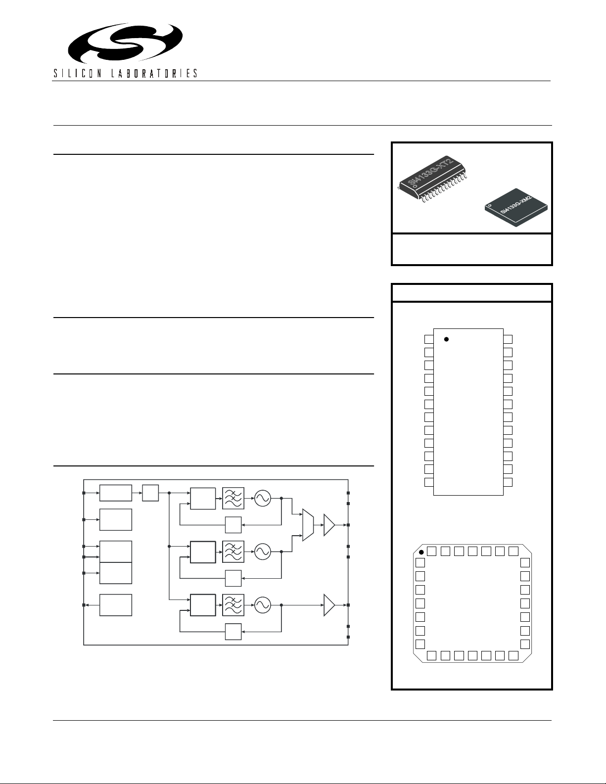
Description
The Si4133G-X2 is a monolithic integrated circuit that performs both IF and
dual-band RF synthesis for GSM and GPRS wireless communications
applications. The Si4133G-X2 includes three VCOs, loop filters, reference
and VCO dividers, and phase detectors. Divider an d power down settings
are programmable through a three-wire serial interface.
Functional Block Diagram
XIN
PWDNB
SDATA
SCLK
SENB
UXOUT
Reference
Amplifier
Power
Down
Control
Serial
Interface
22-bit
Data
Register
Test
Mux
÷
65
Phase
Detector
Phase
Phase
Phase
Phase
Phase
Detector
Detector
Detector
Detector
Detector
Phase
Phase
Phase
Phase
Detector
Detector
Detector
Detector
RF1
÷
N
RF2
÷
N
IF
÷
N
RFLA
RFLB
RFOUT
RFLC
RFLD
IFOUT
IFLA
IFLB
VCO
S
Si4133G-XT2
Ordering Information
See page 27.
Pin Assignments
Si4133G-XT2
SCLK
1
SDATA
RFOUT
GNDR
RFLD
RFLC
GNDR
RFLB
RFLA
GNDR
GNDR
VDDR
2
3
4
5
6
7
8
9
10
11
12
Si4133G-XM2
GNDR
SDATA
1
GNDR
2
RFLD
3
RFLC
4
GNDR
5
RFLB
6
RFLA
7
GNDR
8 9 10 11 12 13 14
SCLK
SENB
VDDI
SENB
24
VDDI
23
IFOUT
22
GNDI
21
IFLB
20
IFLA
19
GNDD
18
VDDD
17
GNDD
16
XIN
15
PWDNB
14
AUXOUT
13
IFOUT
GNDI
22232425262728
21
GNDI
20
IFLB
19
IFLA
18
GNDD
17
VDDD
16
GNDD
15
XIN
GNDR
RFOUT
VDDR
PWDNB
AUXOUT
GNDD
GNDR
Patents pending
Rev. 0.9 8/00 Copyright © 2000 by Silicon Laboratories Si4133GX2-DS09
This information applies to a product under development. Its characteristics and specifications are subject to change without notice.
Page 2

Si4133G-X2
2 Rev. 0.9
Page 3

Si4133G-X2
T
ABLE OF
C
ONTENTS
Section Page
Electrical Specifications. . . . . . . . . . . . . . . . . . . . . . . . . . . . . . . . . . . . . . . . . . . . . . . . . . 4
Functional Description . . . . . . . . . . . . . . . . . . . . . . . . . . . . . . . . . . . . . . . . . . . . . . . . . . 15
Serial Interface . . . . . . . . . . . . . . . . . . . . . . . . . . . . . . . . . . . . . . . . . . . . . . . . . . . . . . 15
Setting the VCO Center Frequencies . . . . . . . . . . . . . . . . . . . . . . . . . . . . . . . . . . . . . 15
Self-Tuning Algorithm . . . . . . . . . . . . . . . . . . . . . . . . . . . . . . . . . . . . . . . . . . . . . . . . . 16
Output Frequencies . . . . . . . . . . . . . . . . . . . . . . . . . . . . . . . . . . . . . . . . . . . . . . . . . . 17
PLL Loop Dynamics . . . . . . . . . . . . . . . . . . . . . . . . . . . . . . . . . . . . . . . . . . . . . . . . . . 17
RF and IF Outputs . . . . . . . . . . . . . . . . . . . . . . . . . . . . . . . . . . . . . . . . . . . . . . . . . . . 17
Reference Frequency Amplifier . . . . . . . . . . . . . . . . . . . . . . . . . . . . . . . . . . . . . . . . . 18
Power Down Modes . . . . . . . . . . . . . . . . . . . . . . . . . . . . . . . . . . . . . . . . . . . . . . . . . . 18
Auxiliary Output (AUXOUT) . . . . . . . . . . . . . . . . . . . . . . . . . . . . . . . . . . . . . . . . . . . . 18
Control Registers . . . . . . . . . . . . . . . . . . . . . . . . . . . . . . . . . . . . . . . . . . . . . . . . . . . . . . . 20
Pin Descriptions: Si4133G-XT2 . . . . . . . . . . . . . . . . . . . . . . . . . . . . . . . . . . . . . . . . . . . . 25
Pin Descriptions: Si4133G-XM2 . . . . . . . . . . . . . . . . . . . . . . . . . . . . . . . . . . . . . . . . . . . 26
Ordering Guide . . . . . . . . . . . . . . . . . . . . . . . . . . . . . . . . . . . . . . . . . . . . . . . . . . . . . . . . . 27
Package Outline: Si4133G-XT2 . . . . . . . . . . . . . . . . . . . . . . . . . . . . . . . . . . . . . . . . . . . . 28
Package Outline: Si4133G-XM2 . . . . . . . . . . . . . . . . . . . . . . . . . . . . . . . . . . . . . . . . . . . 29
Contact Information . . . . . . . . . . . . . . . . . . . . . . . . . . . . . . . . . . . . . . . . . . . . . . . . . . . . . 32
Rev. 0.9 3
Page 4
Si4133G-X2
Electrical Specifications
Table 1. Recommended Operating Conditions
Parameter Symbol Test Condition Min Typ Max Unit
Ambient Temperature T
Supply Voltage V
Supply Voltages Difference V
Note: All minimum and maximum specifications are guaranteed and apply across the recommended operating conditions.
Typical values apply at 3.0 V and an operating temperature of 25°C unless otherwise stated.
Table 2. Absolute Maximum Ratings
1,2
DD
A
(V
∆
(V
DDR
DDI
– V
– V
DDD
DDD
),
)
–20 25 85 °C
2.7 3.0 3.6 V
–0.3 — 0.3 V
Parameter Symbol Value Unit
DC Supply Voltage V
Input Current
Input Voltage
3
3
Storage Temperature Range T
Notes:
1. Permanent device damage may occur if the above Absolute Maximum Ratings are exceeded. Functional operation
should be restricted to the conditions as specified in the operational sections of this data sheet. Exposure to absolute
maximum rating conditions for extended periods may affect device reliability.
2. This device is a high performan ce RF integrated circ uit with an ESD rating of < 2 kV. Handling and assembly of
this device should only be done at ESD-protected workstations.
3. For signals SCLK, SDATA, SENB, PWDNB and XIN.
I
V
DD
IN
IN
STG
–0.5 to 4.0 V
±10 mA
-0.3 to VDD+0.3 V
–55 to 150
o
C
4 Rev. 0.9
Page 5
Table 3. DC Characteristics
(VDD = 2.7 to 3.6 V, TA = –20 to 85°C
Parameter Symbol Test Condition Min Typ Max Unit
Total Supply Current
RF1 Mode Supply Current
RF2 Mode Supply Current
IF Mode Supply Current
1
1
1
1
Si4133G-X2
RF1 and IF operating — 18 31 mA
—1317mA
—1217mA
—1014mA
Standby Current PWDNB = 0,
XPDM = 0
High Level Input Voltage
Low Level Input Voltage
High Level Input Current
Low Level Input Current
High Level Output Voltage
Low Level Output Voltage
Notes:
1. RF1 = 1.55 GHz, RF2 = 1.2 GHz, IF = 1080 MHz, RFPWR = 1
2. For signals SCLK, SDATA, SENB, and PWDNB.
3. For signal AUXOUT.
2
2
2
2
3
3
V
IH
V
IL
I
IH
I
IL
V
OH
V
OL
=
V
3.6 V,
IH
V
= 3.6 V
DD
=
V
0 V,
IL
=
V
3.6 V
DD
IOH = –500 µA VDD–0.4 — — V
IOH = 500 µA — — 0.4 V
—1—µA
0.7 V
DD
— — 0.3 V
——V
DD
V
–10 — 10 µA
–10 — 10 µA
Rev. 0.9 5
Page 6
Si4133G-X2
t
t
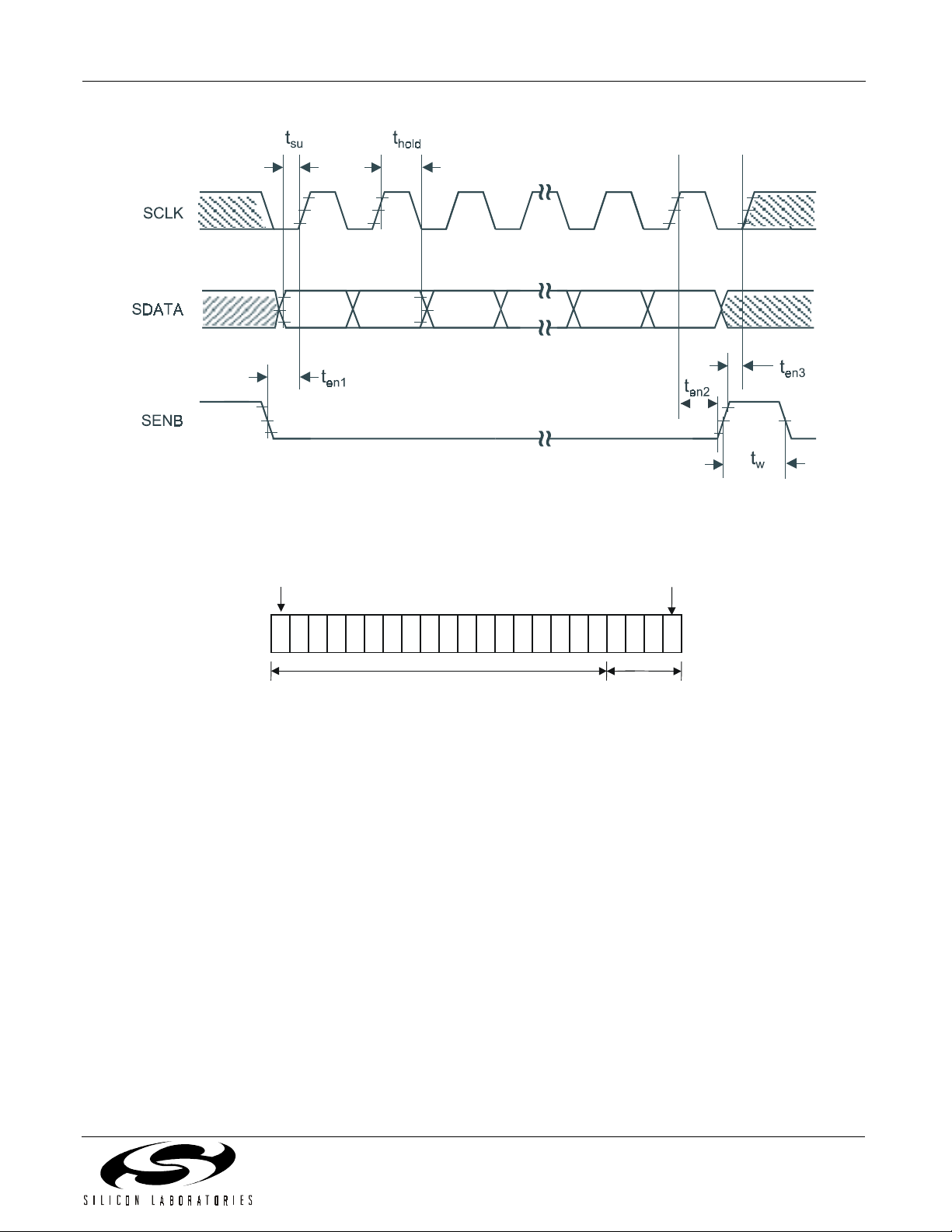
Table 4. Serial Interface Timing
(VDD = 2.7 to 3.6 V, TA = –20 to 85°C)
Parameter
1
SCLK Cycle Time t
SCLK Rise Time t
SCLK Fall Time t
SCLK High Time t
SCLK Low Time t
SDATA Setup Time to SCLK↑
SDATA Hold Time from SCLK↑
SENB↓ to SCLK↑ Delay Time
SCLK↑ to SENB↑ Delay Time
SENB↑ to SCLK↑ Delay Time
2
2
2
2
2
SENB Pulse Width t
Symbol Test Condition Min Typ Max Unit
Figure 1 40 — — ns
Figure 1 — — 50 ns
Figure 1 — — 50 ns
Figure 1 10 — — ns
Figure 1 10 — — ns
Figure 2 5 — — ns
Figure 2 0 — — ns
Figure 2 10 — — ns
Figure 2 12 — — ns
Figure 2 12 — — ns
Figure 2 10 — — ns
t
t
hold
t
t
t
clk
r
f
h
l
su
en1
en2
en3
w
Notes:
1. All timing is referenced to the 50% level of the waveform, unless otherwise noted.
2. Timing is not referenced to 50% level of waveform. See Figure 2.
SCLK
r
80%
50%
20%
f
t
h
t
t
l
clk
Figure 1. SCLK Timing Diagram
6 Rev. 0.9
Page 7
Si4133G-X2
D
17
D
16
D
15
Figure 2. Serial Interface Timing Diagram
First bit
clocked in
D17D16D15D14D13D12D11D10D9D8D7D6D5D4D3D2D1D0A3A2A
data
field
Figure 3. Serial Word Format
A
1
clocked in
address
field
A
0
Last bit
A
1
0
Rev. 0.9 7
Page 8
Si4133G-X2
Table 5. RF and IF Synthesizer Characteristi cs
(VDD = 2.7 to 3.6 V, TA = –20 to 85°C)
Parameter
1
XIN Input Frequency f
Reference Amplifier Sensitivity V
Symbol Test Condition Min Typ Max Unit
REF
REF
—13—MHz
0.5 — VDD
V
P-P
+0.3
Internal Phase Detector Frequency f
RF1 VCO Center Frequency Range f
RF2 VCO Center Frequency Range f
IFOUT Center Frequency f
Tuning Range from f
CEN
φ
CEN
CEN
CEN
f
φ
Note: L
= f
/R 200 KHz
REF
947 — 1720 MHz
789 — 1429 MHz
—1080— MHz
±10% –5 — +5%
EXT
RF1 VCO Pushing Open loop — 0.5 — MHz/V
RF2 VCO Pushing — 0.4 — MHz/V
IF VCO Pushing — 0.3 — MHz/V
RF1 VCO Pulling VSWR = 2:1, all
RF2 VCO Pulling — 0.1 — MHz
phases, open loop
IF VCO Pulling — 0.1 — MHz
—0.4—MHz
p-p
p-p
p-p
RF1 Phase Noise 1 MHz offset — –132 — dBc/Hz
3 MHz offset — –142 — dBc/Hz
RF2 Phase Noise 1 MHz offset — –134 — dBc/Hz
3 MHz offset — –144 — dBc/Hz
IF Phase Noise 100 kHz offset — –117 — dBc/Hz
RF1 Integrated Phase Error 100 Hz to 100 kHz — 0.9 — deg rms
RF1 Harmonic Suppression Second Harmonic — –26 dBc
RF2 Harmonic Suppressio n — –26 dB c
IF Harmonic Suppression — –26 dBc
RFOUT Power Level Z
IFOUT Power Level
Notes:
1. RF1 = 1.55 GHz, RF2 = 1.4 GHz, IF = 1080 MHz., RFPWR=0 for all parameters unless otherwise noted.
2. From power up request (PWDNB↑ or SENB↑ during a write of 1 to bits PD AB, PDIB , and PDRB in regi ster 2) to RF and
IF synthesizers ready (settled to within 0.1 ppm frequency error). Typical settling time to 5 degrees phase error is
120 µs.
3. From power down re quest (PWDNB↓, or SENB↑ during a write of 0 to bits PDAB, PDIB, and PDRB in register 2) to
supply current equal to I
PWDN
.
= 50 Ω –7 –2 1 dBm
L
ZL = 50 Ω
–10 –6 –3 dBm
8 Rev. 0.9
Page 9
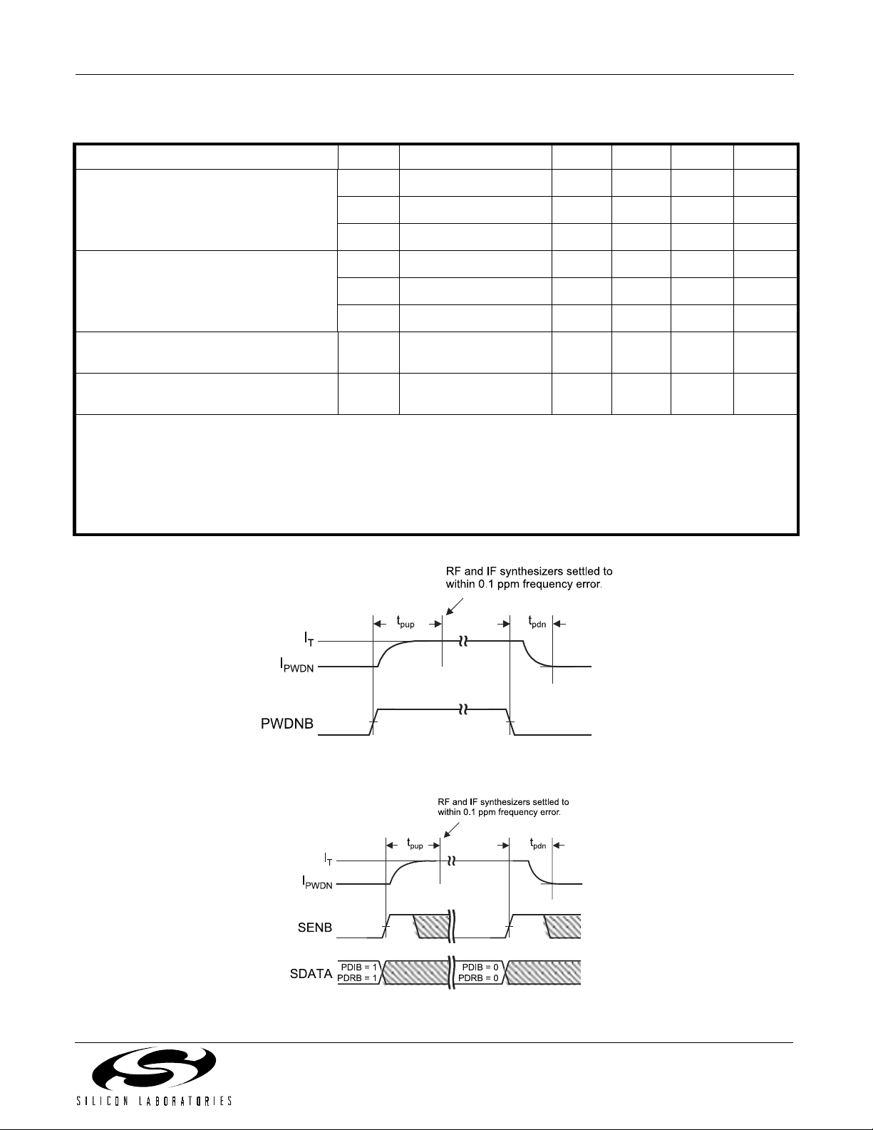
Table 5. RF and IF Synthesizer Characteristics (Continued)
(VDD = 2.7 to 3.6 V, TA = –20 to 85°C)
Si4133G-X2
Parameter
1
Symbol Test Condition Min Typ Max Unit
RF1 Reference Spurs Offset = 200 kHz — –70 — dBc
Offset = 400 kHz — –75 — dBc
Offset = 600 kHz — –80 — dBc
R
F2 Reference Spurs Offset = 200 kHz — –75 — dBc
Offset = 400 kHz — –80 — dBc
Offset = 600 kHz — –80 — dBc
Power Up Request to Synthesizer
Ready Time, RF1, RF2, IF
2
Power Down Request to Synthesizer
Off Time
Notes:
3
1. RF1 = 1.55 GHz, RF2 = 1.4 GHz, IF = 1080 MHz., RFPWR=0 for all parameters unless otherwise noted.
2. From power up request (PWDNB↑ or SENB↑ during a write of 1 to bits PD AB, PDIB , and PDRB in regi ster 2) to RF and
IF synthesizers ready (settled to within 0.1 ppm frequency error). Typical settling time to 5 degrees phase error is
120 µs.
3. From power down re quest (PWDNB↓, or SENB↑ during a write of 0 to bits PDAB, PDIB, and PDRB in register 2) to
supply current equal to I
PWDN
.
t
t
pup
pdn
Figures 4, 5 — 140 — µs
Figures 4, 5 — — 100 ns
Figure 4. Hardware Power Management Timing Diagram
Figure 5. Software Power Management Timing Diagram
Rev. 0.9 9
Page 10
Si4133G-X2
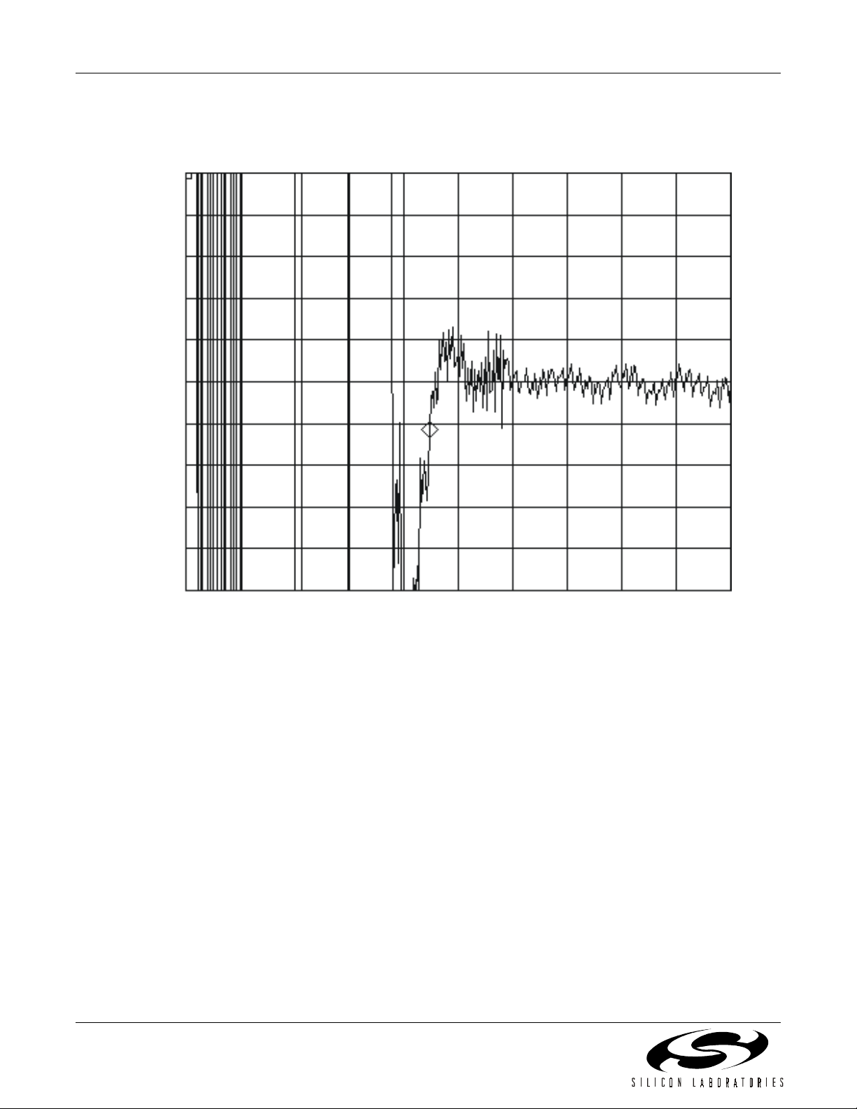
TRACE A: Ch1 FM Gate Time
A Offset us
800
Hz
Real
160
Hz
/div
-461.24
kHz133.59375
-800
Hz
Start: 0 s Stop: 299.21875 us
Figure 6. Typical Transient Response RF1 at 1.6 GHz with
200 kHz Phase Detector Update Frequency
10 Rev. 0.9
Page 11

Si4133G-X2
Figure 7. Typical RF1 Phase Noise at 1.6 GHz with 200 kHz
Phase Detector Update Frequency
Figure 8. Typical RF1 Spurious Response at 1.6 GHz with 200 kHz
Phase Detector Update Frequency
Rev. 0.9 11
Page 12

Si4133G-X2
Figure 9. Typical RF2 Phase Noise at 1.2 GHz with 200 kHz
Phase Detector Update Frequency
Figure 10. Typical RF2 Spurious Response at 1.2 GHz with 200 kHz
Phase Detector Update Frequency
12 Rev. 0.9
Page 13

Si4133G-X2
Figure 11. Typical IF Phase Noise at 1080 MHz with 200 kHz
Phase Detector Update Frequency
Figure 12. IF Spurious Response at 1080 MHz with 200 kHz
Phase Detector Update Frequency
Rev. 0.9 13
Page 14

Si4133G-X2
Printed Trace
Inductors
RFOUT
From
System
Controller
From
System
Controller
560pF 2nH
Si4133G-XT2
SENB
VDDI
IFOUT
GNDI
IFLB
IFLA
GNDD
VDDD
GNDD
XIN
24
0.022 F
Vdd
23
22
21
20
19
18
0.022 F
Vdd
17
16
15
14
13
0.022 F
Vdd
10
11
12
1
2
3
4
5
6
7
8
9
SCLK
SDATA
GNDR
RFLD
RFLC
GNDR
RFLB
RFLA
GNDR
GNDR
RFOUT
VDDR
PWDNB
AUXOUT
Figure 13. Typical Application Circuit: Si4133G-XT2
Vdd
0.022 F
22232425262728
Printed Trace
Inductor or
Chip Inductor
560pF
10nH
560pF10nH
IFOUT
560pF
External Clock
PDWNB
AUXOUT
IFOUT
Printed Trace
Inductors
PWDNB
1
2
3
4
5
6
7
GNDR
GNDR
RFLD
RFLC
GNDR
RFLB
RFLA
GNDR
GNDR
8 9 10 11 12 13 14
Vdd
0.022 F
SCLK
SDATA
Si4133G-XM2
GNDR
RFOUT
SENB
VDDR
VDDI
AUXOUT
IFOUT
PWDNB
GNDI
GNDI
IFLB
IFLA
GNDD
VDDD
GNDD
GNDD
XIN
21
20
19
18
17
16
15
Vdd
Figure 14. Typical Application Circuit: Si4133G-XM2
Printed Trace
Inductor or
Chip Inductor
0.022 F
560pF
560pF
2nH
External Clock
AUXOUT
RFOUT
14 Rev. 0.9
Page 15

Si4133G-X2
Functional Description
The Si4133G-X2 is a monolithic integrated circuit that
performs IF and dual-band RF synthesis for many
wireless applica tions such as GS M900, DCS1800, an d
PCS1900. Its fast transient response also makes the
Si4133G-X2 especially well suited to GPRS and
HSCSD multislot applica tions where channel switching
and settling times are critical. This integrated circuit
(IC), with a minimum number of external components, is
all that is necessary to implement the frequency
synthesis function.
The Si4133G-X2 has three complete phase-locked
loops (PLLs) with integrated voltage-controlled
oscillators (VCOs). The low phase noise of the VCOs
makes the Si4133G-X2 suitable for use in demanding
cellular applications. Also integrated are phase
detectors, loop filter s, and reference divi ders. The IC is
programmed through a three-wire serial interface.
One PLL is provided for IF synthes is, a nd two PL Ls are
provided for dual-band RF synthesis. One RF VCO is
optimized to have its center frequency set between
947 MHz and 1720 MHz, whil e the second RF VCO is
optimized to have its center frequency set between
789 MHz and 1429 MHz. Each RF PLL can adjust its
output frequency by ±5% relative to its VCO’s center
frequency. The IF VCO is optimize d to have its center
frequency set to 1080 MHz. Three settings are provided
for IF output frequencies of 1070.4 MHz, 1080 MHz and
1089.6 MHz.
The center frequency of each of the thr ee VCOs is set
by connection of an external inductance. Inaccuracies in
the value of the inductance are comp ensated for by th e
Si4133G-X2’s proprietary self-tuning algorithm. This
algorithm is initia ted each time the PLL is powered-up
(by either the PW DNB pin or by software) and /or each
time a new output frequency is programmed.
The two RF PLLs share a common output pin, so only
one PLL is active at a given time. Because the two
VCOs can be set to have widely separated center
frequencies, the RF output can be programmed to
service different frequency bands, thus making the
Si4133G-X2 ideal for use in dual-band cellular
handsets.
The unique PLL architecture used in the Si4133G-X2
produces a transient r esponse that is supe rior in speed
to fractional-N architectures without suffering the high
phase noise or spurious modulation effects often
associated with those designs.
Serial Inte rface
The Si4133G-X2 is programmed serially with 22-bit
words comprised of 18 -bit data fie lds and 4-bit address
fields. Figure 3 on page 7 shows the format of the serial
interface. A timing diagr am for the serial word is shown
in Figure 2 on page 7.
When the serial interface is enabled (i.e., when SENB is
low) data and address bits on the SDATA pin are
clocked into an internal s hift register on the risin g edge
of SCLK. Data in the shift re gis ter i s t hen trans fer red o n
the rising edge of SENB into the internal data register
addressed in the address field. The serial word is
disabled when SENB is high.
Table 9 on page 20 summarizes the data register
functions and addresses. It is not necessary (although it
is permissible) to clock into the internal shift register any
leading bits that are “don’t cares”.
Setting the VCO Center Frequencies
The PLLs can adju st the IF and RF outp ut frequencies
±5% with respect to their VCO center frequencies. Each
center frequency is established by the value of an
external inductance connected to the respective VCO.
Manufacturing tolerances of ±10% for the external
inductances are acceptable. The Si4133G-X2 will
compensate for inaccuracies in each inductance by
executing a self-tu ning algorithm following power-up or
following a change in the programmed output
frequency.
Because the total tank inductance is in the low nH
range, the inductance of the package needs to be
considered in determining the correct external
inductance. The total inductance (L
each VCO is the su m of the externa l inductanc e (L
and the package i nductance (L
nominal capacitance (C
inductance, and the center frequency is as follows:
F
CEN
NOM
--------------------------------------------=
2π L
or
F
CEN
-------------------------------------------------------------------- -=
2π L
PKG
) in parallel with the total
1
TOTCNOM
1
+()C
PKGLEXT
) presented to
TOT
). Each VCO has a
EXT
⋅
⋅
NOM
)
Rev. 0.9 15
Page 16

Si4133G-X2
Tables 6 and 7 summarize these characteristics for
each VCO.
Table 6. Si4133G-XT2 VCO Characteristics
VCO f
RF1 947 1720 4.3 2.0 0.0 4.6
RF2 789 1429 4.8 2.3 0.3 6.2
IF 1080 6.5 2.1 1.2
Range
CEN
(MHz)
Min Max Min Max
Cnom
(pF)
Lpkg
(nH)
Lext Range
(nH)
Table 7. Si4133G-XM2 VCO Characteristics
VCO f
RF1 947 1720 4.3 1.5 0.5 5.1
RF2 789 1429 4.8 1.5 1.1 7.0
IF 1080 6.5 1.6 1.7
Range
CEN
(MHz)
Min Max Min Max
Si4133G-XM2
Cnom
(pF)
L
PKG
2
L
PKG
2
Lpkg
(nH)
Lext Range
(nH)
L
EXT
Figure 15. External Inductance Connection
As a design example, suppose it is desired to
synthesize frequencies in a 25 MHz band between
1120 MH z and 1145 MHz. The cente r frequency shoul d
be defined as midway between the two extremes, or
1132.5 MHz. The PLL will be able to adjust the VCO
output frequency ±5% of the center frequency, or
±56.6 MHz of 1132.5 MHz (i.e., from approximately
1076 MHz to 1189 MHz, more than enough for this
example). The RF2 VCO has a C
4.1 nH in ductance (corre ct to two digits) in paral lel with
this capacitance w ill yield the desired c enter frequen cy.
An external inductan ce of 1.8 nH sh ould be connected
of 4.8 pF, and a
NOM
between RFLC and RFLD a s shown in Figure 15. This ,
in addition to 2.3 nH of package inductance, will present
the correct total inductance to the VCO. In
manufacturing, the extern al inductance can vary ±10%
of its nominal valu e and the S i4133G- X2 will c orrect for
the variation with the self-tuning algorithm.
In most cases the requisite value of the external
inductance is small enough to allow a PC board trace to
be utilized. During initial board layout, a le ngth of trace
approximating the d esired inducta nce can be used. F or
more information, please refer to Application Note 31.
Self-Tuning Algorithm
The self-tuning algorithm is initiated immediately
following power-up of a PLL or, if the PLL is already
powered, following a c hange in its programmed o utput
frequency. This algorithm attempts t o tune the VCO so
that its free-running frequency is near the desired output
frequency. In so doing, the algorithm will compensate
for manufacturing tolerance errors in the value of the
external inductance conn ected to the VCO. It will also
reduce the frequency error for which the PLL must
correct to get the prec ise desi red ou tput fr equency. The
self-tuning algorith m will leave the VCO oscillating at a
frequency in error by somewhat less than 1% of the
desired output frequency.
After self-tuning, the PLL controls the VCO oscillation
frequency. The PLL will complete frequency locking,
eliminating any remaining frequency error. Thereafter, it
will maintain frequency-lock, compensating for effects
caused by temperature and supply voltage variations.
The Si4133G-X2’s self-tuning algorithm will
compensate for component value errors at any
temperature within the specified temperature range.
However, the ability of the PLL to compensate for drift in
component values that occur AFTER self-tuning is
limited. For external inductances with temperature
coefficients around ±150 ppm/
maintain lock for changes in temperature of
approximately ±30
o
C.
Applications where the PLL is regularly powere d down
or switched between channels minimize or eliminate the
potential effects of temperature drift because the VCO is
re-tuned when it is powered up or when a new
frequency is programmed. In applications where the
ambient temperature can drift substantially after selftuning, it may be necessary to monitor the LDETB (lockdetect bar) signal on the AUXOU T pin to determine the
locking state of the PLL. (See the AUXILIARY OUTPUT
section below for how to select LDETB.)
The LDETB signal will be low after self-tuning has
completed but will rise when either the IF or RF PLL
o
C, the PLL will be able to
16 Rev. 0.9
Page 17

Si4133G-X2
nears the limit of its compensation range (LDETB will
also be high when either PLL is executing the selftuning algorithm). The output frequency will still be
locked when LDETB goes high, but the PLL will
eventually lose loc k if the temper ature conti nues to dr ift
in the same direction. Therefore, if LDETB goes high
both the IF and RF PLLs shoul d promptly be re-tuned
by initiating the self-tuning algorithm.
Output Frequencies
The IF and RF output frequencies are set by
programming the N Divider r egister s. Eac h RF PLL has
its own N register and can be programmed
independently. All three PLL R dividers are fixed at
R=65 to yield a 200 kHz phase detector update rate
from a 13 MHz reference frequen cy. Programm ing the
N divider register for either RF1 or RF2 automatically
selects the associated output.
The reference frequ ency on the XIN pin is divided b y R
and this signal is inpu t to the P LL’s phase detector. The
other input to the phase detector is the PLL’s VCO
output frequency divi ded by N. The PLL acts to make
these frequencies equal. That is, after an initial transient
F
OUT
-------------
N
or
F
OUT
For XIN = 13 MHz this simplifies to
N
------
65
F
------------ -=
REF
65
F
⋅=
REF
update periods, the Si4133G-X2 executes the selftuning algorithm. Ther eafter the PL L control s the outpu t
frequency. Because of the unique architecture of the
Si4133G-X2 PLLs, the ti me re quire d t o s ettl e t he o utpu t
frequency to 0.1 ppm error is ap proximately 21 update
periods. Thus, the total time af ter power -up or a ch ang e
in programmed frequency until the synthesized
frequency is well sett led (including time for self -tuning)
is around 28 update periods or 140 µS.
RF and IF Outputs
The RFOUT and IFOUT pins are driven by amplifiers
that buffer the RF V COs and I F VCO, respe ctively. The
RF output amplifier receives its input from either the
RF1 or RF2 VCO, depending upon which N divider
register was last writte n to. For example, programming
the N divider register for RF1 automatically selects the
RF1 VCO output.
The RFOUT pin mus t be coup led to i ts load through a n
ac coupling capacitor. A matching network is required to
maximize power delivered into a 50 Ω load. The
network consists of a 2 nH series inductance, which
may be realized with a PC board trace, connected
between the RFOUT pin and the ac coupling capacitor.
The network is made to provide an adequate m atch to
an external 50 Ω load for both the RF1 and RF2
frequency bands. Th e matching networ k also filters th e
output signal to reduce harmonic distortion. A 50 Ω load
is not required for proper operation of the Si4133G-X2.
Depending on transceiver requirements, the matching
network may not be needed. See Figure 16 below.
F
OUT
The integer N is s et by pr ogramm ing th e RF1 N Div ider
register (register 3), the RF2 N Divi der regi ster (reg ister
4), and the IF N Divider register (register 5).
Each N divider is im plemented as a conventional hig h
speed divider. That is, it consists of a dual-modulus
prescaler, a swallow counter, and a lower speed
synchronous counter. However, the calculation of thes e
values is done automatically. Only the appropriate N
value needs to be programmed
N200kHz⋅=
PLL Loop Dynamics
The transient response for each PLL has been
optimized for a GSM application. VCO gain, phase
detector gain, and loop filter characteristics are not
programmable.
The settling time for eac h PLL is direc tly proportio nal to
its phase detector update period Tφ (Tφ equals 1/fφ). For
a GSM application with a 13 MHz reference frequen cy,
the RF and IF PLLs Tφ =5µS. During the first 6.5
Rev. 0.9 17
2 nH 560 pF
RFOUT
50Ω
Figure 16. RFOUT 50ΩΩΩΩ Test Circuit
The RF output power is controlled with th e RFPWR bit
in register 0. Setting this bit increases the supply current
by approximately 1.2 mA. To minimize output power
variation over temp erature, the RFPWR bit can be set
as a function of temperature. For example, set
RFPWR=1 for temperatures greater than 50
otherwise set RFPWR=0.
The IFOUT pin must al so be c ou pl ed to its l oad t hr oug h
an ac coupling capacitor. A matching network is also
required in order to drive a 50 Ω load. See Figure 17
below.
o
C
,
Page 18

Si4133G-X2
18 nH 560 pF
IFOUT
50
Figure 17. IFOUT 50ΩΩΩΩ Matching Network
Reference Frequency Amplifier
The Si4133G-X2 provides a reference frequency
amplifier. If the driving signal has CMOS levels it can be
connected directly to the XIN pin. Otherwise, the
reference frequenc y signal sho uld be ac co upled to the
XIN pin through a 100 pF capacitor.
Power Down Modes
Tabl e 8 summarizes the power down functionality. The
Si4133G-X2 can be powered down by taking the
PWDNB pin low or by setting bits in the Power Down
register (registe r 2). When the PWDNB pin is low, the
Si4133G-X2 will be powered down regardless of the
Power Down registe r setti ngs. W hen t he PW DNB pin is
high, power management is under cont rol of the Po wer
Down register bits.
It may be desirable to defeat power down of the
reference frequency amplifier. In such a case the XPDM
(XTAL Power Down Mode) bit in the Mai n Confi gu ra tio n
register (register 0) should be set to 1. The refe rence
frequency amplifier will then remain powered up even
when the PWDNB pin is asserted (i.e., low), excepting
when all three of the Power Down register b its (PDAB,
PDIB, and PDRB) are low. This exception exists so that,
even in this mode, the reference amplifier can be forced
to power down if sufficient time occurs for a power down
and power up sequence. Alternatively, the reference
amplifier power down defeat mode can be exited by
setting XPDM to 0.
With the PWDNB pin high, the XPDM bit has no effect.
The reference frequen cy amplifier, IF, and RF sections
of the Si4133G-X2 cir cuitry can be indivi duall y powere d
down by setting the Power Down register bits PDAB,
PDIB, and PDRB low, respectively. Note that the
reference frequency a mplifier will also b e powered up if
either the PDRB and PDIB bits are high, even if the
PDAB bit is low. Also, setting the AUTOPDB bi t to 1 in
the Main Configuratio n re gi ste r (r egi st er 0 ) is e qui va len t
to setting all three of the bits in the Power Down register
to 1. The serial in terface remains available and ca n be
written in all power down modes.
Auxiliary Output (AUXOUT)
The AUXOUT pin can be used to mo nitor a variety of
signals. The sign al appearing on AUXOUT is se lected
by setting the AUXSEL bits in the Main Configuration
register (register 0). The possible outputs are liste d in
the description of the Main Configuration register.
Some of these signals may only be useful for evaluation
purposes (in particular, the PLL R-divider and N-divider
outputs). Two signals, have more general use. The first is
the LDETB signal, which can be selected by setting the
AUXSEL bits to 011. As discussed previously, this signal
can be used to indicate that the IF or RF PLL is about to
lose lock due to excessive ambient temperature drift and
should be re-tuned. The second is the Reference Clock
output. This is a buffered version of the signal on the XIN
pin, with the exception that it will be held low when the
reference frequency amplifier is powered down.
18 Rev. 0.9
Page 19

Table 8. Power Down Configuration
PWDNB Pin AUTOPDB PDIB PDRB
PWDNB = 0
X X X OFF OFF OFF
0 0 0 OFF OFF OFF
001ONOFFON
Reference
Frequency
Amplifier
Si4133G-X2
IF Circuitry RF Circuitry
PWDNB = 1
Note: The XPDM bit has no effect when the PWDNB pin is high.
010ONONOFF
0 11ONONON
000ONOFFOFF
1 xxONONON
Rev. 0.9 19
Page 20

Si4133G-X2
Control Registers
T a ble 9. Register Summary
Register Name Bit 17Bit 16Bit 15Bit 14Bit 13Bit 12Bit 11Bit 10Bit 9Bit 8Bit 7Bit 6Bit 5Bit 4Bit3Bit 2Bit 1Bit
0
0 Main
Configuration
XXX AUXSEL 0000000 0
AUTO
010
PDB
1 Reserved
2 Power DownXXXXXXXXXXXXXX X 0
3RF1 N
N
RF1
PDIB PDRB
Divider
4RF2 N
XN
RF2
Divider
5 IF N Divider X X N
IF
6 Reserved
7 Reserved
.
.
.
15 Reserved
Note: X = Don’t Care. Registers 1 and 6–15 are reserved. Writes to these registers may result in unpredictable behavior. Any
register not listed here is reserved and should not be written.
20 Rev. 0.9
Page 21

Si4133G-X2
Register 0. Main Configuration Address Field = A[3:0] = 0000
Bit D17 D16 D15 D14 D13 D12 D11 D10 D9 D8 D7 D6 D5 D4 D3 D2 D1 D0
Name XXX AUXSEL 00000000
Bit Name Function
17:15 Reserved Don’t care.
14:12 AUXSEL Auxiliary Output Pin Definition.
000 = Reserved.
001 = Force output low.
010 = CMOS level of f
REF
.
011 = Lock Detect—LDETB.
100 = CMOS level of f
101 = CMOS level of f
110 = CMOS level of f
111 = CMOS level of f
of active RF synthesizer.
φ
R
of IF synthesizer.
φ
R
of active RF synthesizer.
φ
N
of IF synthesizer.
φ
N
11:5 Reserved Program to zero.
4 Reserved Program to zero.
3 AUTOPDB Auto Power Down
0 = Software powerdown is controlled by register 2.
1 = Equivalent to setting all bits in register 2 = 1.
2 Reserved Program to zero.
AUTO
PDB
010
1 Reserved Program to one.
0 Reserved Program to zero.
Rev. 0.9 21
Page 22

Si4133G-X2
Register 2. Power Down Address Field (A[3:0]) = 0010
Bit D17 D16 D15 D14 D13 D12 D11 D10 D9 D8 D7 D6 D5 D4 D3 D2 D1 D0
Name XXXXXXXXXXXXXXX X
PDIB PDRB
Bit Name Function
17:2 Reserved Don’t care.
1PDIBPower Down IF Synthesizer.
0 = IF synthesizer powered down.
1 = IF synthesizer on.
0 PDRB Power Down RF Synthesizer.
0 = RF synthesizer powered down.
1 = RF synthesizer on.
Register 3. RF1 N Divider Address Field (A[3:0]) = 0011
Bit D17D16D15D14D13D12D11D10D9D8D7D6D5D4D3D2D1D0
Name N
RF1
Bit Name Function
17:0 N
RF1
N Divider for RF1 Synthesizer.
Register 4. RF2 N Divider Address Field = A[3:0] = 0100
Bit D17D16D15D14D13D12D11D10D9D8D7D6D5D4D3D2D1D0
Name XN
RF2
Bit Name Function
17 Reserved Don’t care.
16:0 N
22 Rev. 0.9
RF2
N Divider for RF2 Synthesizer.
Page 23

Si4133G-X2
Register 5. IF N Divider Address Field (A[3:0]) = 0101
Bit D17D16D15D14D13D12D11D10D9D8D7D6D5D4D3D2D1D0
Name XX N
Name Function
17:16 Reserved Don’t care.
15:0 N
IF
N Divider for IF Synthesizer.
Only the following values are allowed (frequencies assume XIN is 13
MHz):
7150 = 1070.4 MHz
7215 = 1080.0 MHz
7280 = 1089.6 MHz
IF
Rev. 0.9 23
Page 24

Si4133G-X2
<15 ns
Figure 18. AUXOUT Timing Diagram
24 Rev. 0.9
Page 25

Pin Descriptions: Si4133G-XT2
Si4133G-X2
SCLK
SDATA
GNDR
RFLD
RFLC
GNDR
RFLB
RFLA
GNDR
GNDR
RFOUT
VDDR
1
2
3
4
5
6
7
8
9
10
11
12
24
23
22
21
20
19
18
17
16
15
14
13
SENB
VDDI
IFOUT
GNDI
IFLB
IFLA
GNDD
VDDD
GNDD
XIN
PWDNB
AUXOUT
Name Pin Number(s) Description
AUXOUT 13 Auxiliary output
GNDD 16, 18 Common ground for digital circuitry
GNDI 21 Common ground for IF analog circuitry
GNDR 3, 6, 9, 10 Common ground for RF analog circuitry
IFLA, IFLB 19, 20 Pins for inductor connection to IF VCO
IFOUT 22 Intermediate frequency (IF) output of the IF VCO
PWDNB 14 Power down input pin
RFLA, RFLB 7, 8 Pins for inductor connection to RF1 VCO
RFLC, RFLD 4, 5 Pins for inductor connection to RF2 VCO
RFOUT 11 Radio frequency (RF) output of the selected RF VCO
SCLK 1 Serial clock input
SDATA 2 Serial data input
SENB 24 Enable serial port input
VDDD 17 Supply voltage for digital circuitry
VDDI 23 Supply voltage for IF analog circuitry
VDDR 12 Supply voltage for the RF analog circuitry
XIN 15 Reference frequency amplifier input
Rev. 0.9 25
Page 26

Si4133G-X2
Pin Descriptions: Si4133G-XM2
GNDR
SDATA
SCLK
SENB
VDDI
IFOUT
GNDI
22232425262728
GNDR
RFLD
RFLC
GNDR
RFLB
RFLA
GNDR
1
2
3
4
5
6
7
8 9 10 11 12 13 14
GNDR
GNDR
RFOUT
VDDR
AUXOUT
PWDNB
21
20
19
18
17
16
15
GNDD
GNDI
IFLB
IFLA
GNDD
VDDD
GNDD
XIN
Name Pin Number(s) Description
AUXOUT 12 Auxiliary output
GNDD 14, 16, 18 Common ground for digital circuitry
GNDI 21, 22 Common ground for IF analog circuitry
GNDR 1, 4, 7-9, 28 Common ground for RF analog circuitry
IFLA, IFLB 19, 20 Pins for inductor connection to IF VCO
IFOUT 23 Intermediate frequency (IF) output of the IF VCO
PWDNB 13 Power down input pin
RFLA, RFLB 5,6 Pins for inductor connection to RF1 VCO
RFLC, RFLD 2, 3 Pins for inductor connection to RF2 VCO
RFOUT 10 Radio frequency (RF) output of the selected RF VCO
SCLK 26 Serial clock inpu t
SDATA 27 Seri al data in put
SENB 25 Enable serial port input
VDDD 17 Supply voltage for digital circuitry
VDDI 24 Supply voltage for IF analog circuitry
VDDR 11 Supply voltage for the RF analog circuitry
XIN 15 Reference frequency amplifier input
26 Rev. 0.9
Page 27

Ordering Guide
Si4133G-X2
Ordering Part
Number
Si4133G-XM2 RF1 / RF2 / IF OUT 28-Pin MLP –20 to 85
Si4133G-XT2 RF1 / RF2 / IF OUT 24-Pin TSSOP –20 to 85
Description Package Temperature
o
C
o
C
Rev. 0.9 27
Page 28

Si4133G-X2
Package Outline: Si4133G-XT2
B
D
E H
θ
L
A
e
A1
Figure 19. 24-Pin Thin Shrink Small Outline Package (TSSOP)
Table 10. Package Dimensions
Symbol Inches Millimeters
Min Max Min Max
A — 0.047 — 1.1
A1 0.002 0.006 0.05 0.15
B 0.007 0.012 0.19 0.30
C 0.004 0.008 0.09 0.20
D 0.303 0.311 7.70 7.90
E 0.169 0.177 4.30 4.50
e 0.0 26 BS C 0 .65 BS C
H 0.252 BSC 6.40 BSC
C
L 0.018 0.030 0.45 0.75
θ 0° 8° 0° 8°
28 Rev. 0.9
Page 29

Package Outline: Si4133G-XM2
Si4133G-X2
Figure 20. 28-Pin Micro Leadframe Package (MLP)
Table 11. Package Dimensions
Controlling Dimension: mm
Symbol Millimeters
Min Nom Max
A — 0.90 1.00
A1 0.00 0.01 0.05
b 0.18 0.23 0.30
D5.00 BSC
D1 4.75 BSC
E5.00 BSC
E1 4.75 BSC
N28
Nd 7
Ne 7
e0.50 BSC
L 0.50 0.60 0.75
θ
Rev. 0.9 29
12
°
Page 30

Si4133G-X2
N
OTES
:
30 Rev. 0.9
Page 31

Si4133G-X2
N
OTES
:
Rev. 0.9 31
Page 32

Si4133G-X2
Contact Information
Silicon Laborator ies Inc.
4635 Boston Lane
Austin, Texas 78735
Tel:1+ (512) 416-8500
Fax:1+ (512) 416-9669
Toll Free:1+ (877) 444-3032
Email: productinfo@silabs.com
Internet: www.silabs.com
The information in this document is believed to be accurate in all respects at the time of publication but is subject to change without notice.
Silicon Laboratories assumes no responsibility for errors and omissions, and disclaims responsibility for any consequences resulting from
the use of information included herein. Additionally, Silicon Laboratories assumes no responsibility for the functioning of undescribed features or parameters. Silicon Laboratories reserves the right to make changes without further notice. Silicon Laboratories makes no warranty, representation or guarantee regarding the suitability of its products for any particular purpose, nor does Silicon Laboratories assume
any liability arising out of the application or use of any product or circuit, and specifically disclaims any and all liability, including without
limitation consequential or incidental damages. Silicon Laboratories products are not designed, intended, or authorized for use in applications intended to support or sustain life, or for any other application in which the failure of the Silicon Laboratories product could create a
situation where personal injury or death may occur. Should Buyer purchase or use Silicon Laboratories products for any such unintended
or unauthorized application, Buyer shall indemnify and hold Silicon Laboratories harmless against all claims and damages.
Silicon Laboratories and Silicon Labs are trademarks of Silicon Laboratories Inc.
Other products or brandnames mentioned herein are trademarks or registered trademarks of their respective holders.
32 Rev. 0.9
 Loading...