

Page 1
Si4133-BT
查询Si4112供应商
Si4133
Si4123/22/13/12
D
UAL-BAND
F
W
OR
IRELESS COMMUNICATIONS
RF S
YNTHESIZER WITH INTEGRATED
Features
!
Dual-Band RF Synthesizers
RF1: 900 MHz to 1.8 GHz
"
RF2: 750 MHz to 1.5 GHz
"
!
IF Synthesizer
IF: 62.5 MHz to 1000 MHz
"
!
Integrated VCOs, Loop Filters,
Varactors, and Resonators
!
Minimal (2) External
Components Required
!
Low Phase Noise
!
Programmable Power Down Modes
!
1 µA Standby Current
!
18 mA Typical Supply Current
!
2.7 V to 3.6 V Operation
!
Packages: 24-Pin TSSOP, 28-Lead
MLP
Applications
!
Dual-Band Communications
!
Digital Cellular Telephones
GSM, DCS1800, PCS1900
!
Digital Cordless Phones
!
Analog Cordless Phones
!
Wireless LAN and WAN
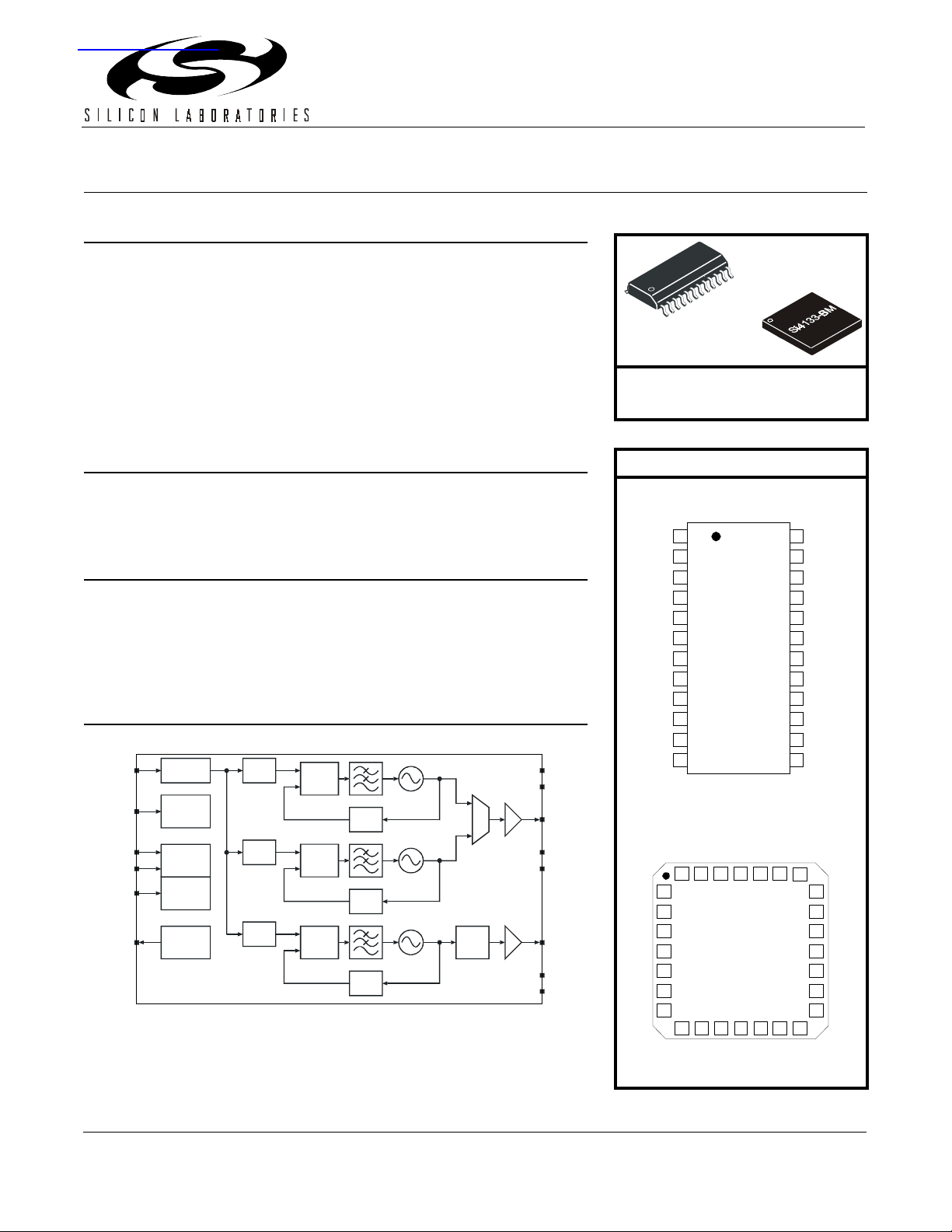
Description
The Si4133 is a mo nolith ic in tegrate d circui t that per forms bo th IF an d dualband RF synthesis for wireless communications applications. The Si4133
includes three VCOs, loop filters, reference and VCO dividers, and phase
detectors. Divider and power-down settings are programmable through a
three-wire serial interface.
Functional Block Diagram
XIN
PWDNB
Reference
Am plifier
Power
Down
Control
÷
R
Phase
Detector
RF1
÷
N
RFLA
RFLB
RFOUT
VCOS
Si4133-BT
Ordering Information:
See page 31.
Pin Assignments
Si4133-BT
SCLK
SDATA
GNDR
RFLD
RFLC
GNDR
RFLB
RFLA
GNDR
GNDR
RFOUT
VDDR
124
223
322
421
520
619
718
817
916
10 15
11 14
12 13
Si4133-BM
SENB
VDDI
IFOUT
GNDI
IFLB
IFLA
GNDD
VDDD
GNDD
XIN
PWDNB
AUXOUT
Rev. 1.1 3/01 Copyright © 2001 by Silicon Laboratories Si4133-DS11
SDATA
SCLK
SENB
AUXOUT IFD I V
Serial
Inte r f ace
22-bit
Data
Register
Test
Mux
÷
R
÷
Phase
Detector
R
Phase
Detector
RF2
÷
N
IF
÷
N
RFLC
RFLD
IFO UT
IFL A
IFL B
VDDI
SCLK
SDATA
GNDR
28 27 26 25 24 23
1
GNDR
2
RFLD
3
RFLC
4
GNDR GNDD
5
RFLB
6
RFLA
7
GNDR
8 9 10 11 12 13 14
VDDR SENB
GNDR
GNDR
RFOUT
AUXOUT
Patents pending
This information applies to a product under development. Its characteristics and specifications are subject to change without notice.
IFOUT
GNDI
22
21
GNDI
20
IFLB
19
IFLA
18
17
VDDD
16
GNDD
15
XIN
GNDD
PWDNB
Page 2

Si4133
2 Rev. 1.1
Page 3

Si4133
T
ABLE OF
C
ONTENTS
Section Page
Electrical Specifications . . . . . . . . . . . . . . . . . . . . . . . . . . . . . . . . . . . . . . . . . . . . . . . . . 4
Functional Description . . . . . . . . . . . . . . . . . . . . . . . . . . . . . . . . . . . . . . . . . . . . . . . . . . 16
Serial Interface . . . . . . . . . . . . . . . . . . . . . . . . . . . . . . . . . . . . . . . . . . . . . . . . . . . . . . 16
Setting the VCO Center Frequencies . . . . . . . . . . . . . . . . . . . . . . . . . . . . . . . . . . . . . 16
Extended Frequency Operation . . . . . . . . . . . . . . . . . . . . . . . . . . . . . . . . . . . . . . . . . 17
Self-Tuning Algorithm . . . . . . . . . . . . . . . . . . . . . . . . . . . . . . . . . . . . . . . . . . . . . . . . . 17
Output Frequencies . . . . . . . . . . . . . . . . . . . . . . . . . . . . . . . . . . . . . . . . . . . . . . . . . . 18
PLL Loop Dynamics . . . . . . . . . . . . . . . . . . . . . . . . . . . . . . . . . . . . . . . . . . . . . . . . . . 18
RF and IF Outputs . . . . . . . . . . . . . . . . . . . . . . . . . . . . . . . . . . . . . . . . . . . . . . . . . . . 19
Reference Frequency Amplifier . . . . . . . . . . . . . . . . . . . . . . . . . . . . . . . . . . . . . . . . . 19
Power Down Modes . . . . . . . . . . . . . . . . . . . . . . . . . . . . . . . . . . . . . . . . . . . . . . . . . . 19
Auxiliary Output (AUXOUT) . . . . . . . . . . . . . . . . . . . . . . . . . . . . . . . . . . . . . . . . . . . . 20
Control Registers . . . . . . . . . . . . . . . . . . . . . . . . . . . . . . . . . . . . . . . . . . . . . . . . . . . . . . . 21
Pin Descriptions: Si4133-BT . . . . . . . . . . . . . . . . . . . . . . . . . . . . . . . . . . . . . . . . . . . . . . 27
Pin Descriptions: Si4133-BM . . . . . . . . . . . . . . . . . . . . . . . . . . . . . . . . . . . . . . . . . . . . . . 29
Ordering Guide . . . . . . . . . . . . . . . . . . . . . . . . . . . . . . . . . . . . . . . . . . . . . . . . . . . . . . . . . 31
Si4133 Derivative Devices . . . . . . . . . . . . . . . . . . . . . . . . . . . . . . . . . . . . . . . . . . . . . . . . 31
Package Outline: Si4133-BT . . . . . . . . . . . . . . . . . . . . . . . . . . . . . . . . . . . . . . . . . . . . . . 32
Package Outline: Si4133-BM . . . . . . . . . . . . . . . . . . . . . . . . . . . . . . . . . . . . . . . . . . . . . . 33
Contact Information . . . . . . . . . . . . . . . . . . . . . . . . . . . . . . . . . . . . . . . . . . . . . . . . . . . . . 34
Rev. 1.1 3
Page 4
Si4133
Electrical Specifications
Table 1. Recommended Operating Conditions
Parameter Symbol Test Condition Min Typ Max Unit
Ambient Temperature T
Supply Voltage V
Supply Voltages Difference V
Note: All minimum and maximum specifications are guaranteed and apply across the recommended operating conditions.
Typical values apply at nominal supply voltages and an operating temperature of 25°C unless otherwise stated.
Table 2. Absolute Maximum Ratings
1,2
DD
A
(V
(V
DDR
DDI
– V
– V
∆
DDD
DDD
),
)
–40 25 85 °C
2.7 3.0 3.6 V
–0.3 — 0.3 V
Parameter Symbol Value Unit
DC Supply Voltage V
Input Current
Input Voltage
3
3
Storage Temperature Range T
Notes:
1. Permanent device damage may occur if the above Absolute Maximum Ratings are exceeded. Functional operation
should be restricted to the conditions as specified in the operational sections of this data sheet. Exposure to absolute
maximum rating conditions for extended periods may affect device reliability.
2. This device is a high performan ce RF integrated circ uit with an ESD rating of < 2 kV. Handling and assembly of
this device should only be done at ESD-protected workstations.
3. For signals SCLK, SDATA, SENB, PWDNB and XIN.
I
V
DD
IN
IN
STG
–0.5 to 4.0 V
±10 mA
–0.3 to VDD+0.3 V
–55 to 150
o
C
4 Rev. 1.1
Page 5
Si4133
Table 3. DC Characteristics
(VDD = 2.7 to 3.6 V, TA = –40 to 85°C)
Parameter Symbol Test Condition Min Typ Max Unit
Total Supply Current
RF1 Mode Supply Current
RF2 Mode Supply Current
IF Mode Supply Current
1
1
1
1
Standby Current PWDNB = 0 — 1 — µA
High Level Input Voltage
Low Level Input Voltage
High Level Input Current
Low Level Input Current
High Level Output Voltage
Low Level Output Voltage
Notes:
1. RF1 = 1.6 GHz, RF2 = 1.1 GHz, IFOUT = 550 MHz, LPWR = 0
2. For signals SCLK, SDATA, SENB, and PWDNB.
3. For signal AUXOUT.
2
2
2
2
3
3
V
IH
V
IL
I
IH
I
IL
V
OH
V
OL
RF1 and IF operating — 18 27 mA
—1016mA
—916mA
—813mA
V
V
V
=
IH
= 3.6 V
DD
V
IL
=
DD
3.6 V,
=
0 V,
3.6 V
0.7 V
DD
— — 0.3 V
–10 — 10 µA
–10 — 10 µA
——V
DD
IOH = –500 µA VDD–0.4 — — V
IOH = 500 µA — — 0.4 V
V
Rev. 1.1 5
Page 6
Si4133
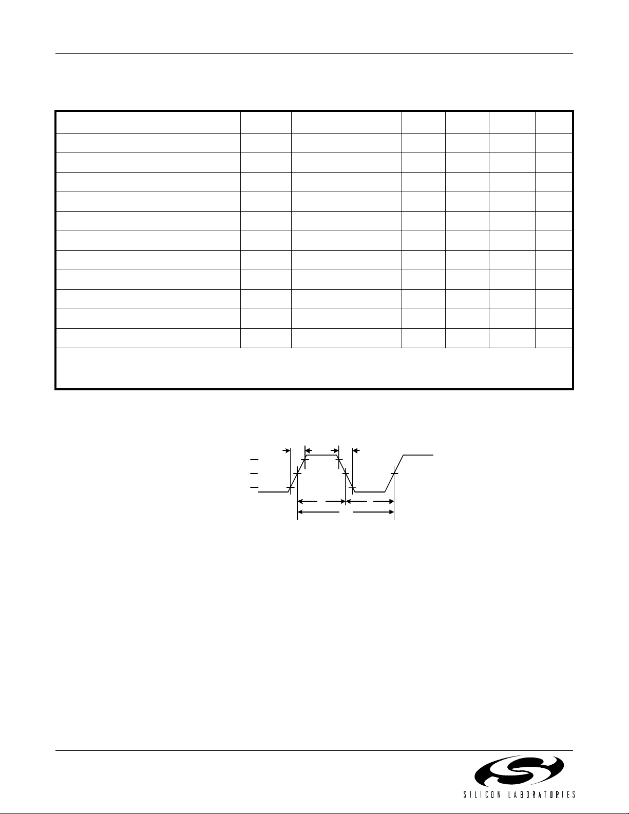
Table 4. Serial Interface Ti ming
(VDD = 2.7 to 3.6 V, TA = –40 to 85°C)
Parameter
1
SCLK Cycle Time t
SCLK Rise Time t
SCLK Fall Time t
SCLK High Time t
SCLK Low Time t
SDATA Setup Time to SCLK↑
SDATA Hold Time from SCLK↑
SENB↓ to SCLK↑ Delay Time
SCLK↑ to SENB↑ Delay Time
SENB↑ to SCLK↑ Delay Time
2
2
2
2
2
SENB Pulse Width t
Symbol Test Condition Min Typ Max Unit
Figure 1 40 — — ns
Figure 1 — — 50 ns
Figure 1 — — 50 ns
Figure 1 10 — — ns
Figure 1 10 — — ns
Figure 2 5 — — n s
Figure 2 0 — — n s
Figure 2 10 — — ns
Figure 2 12 — — ns
Figure 2 12 — — ns
Figure 2 10 — — ns
t
t
t
t
clk
t
su
hold
en1
en2
en3
w
r
f
h
l
Notes:
1. All timing is referenced to the 50% level of the waveforms unless otherwise noted.
2. Timing is not referenced to 50% level of the waveform. See Figure 2.
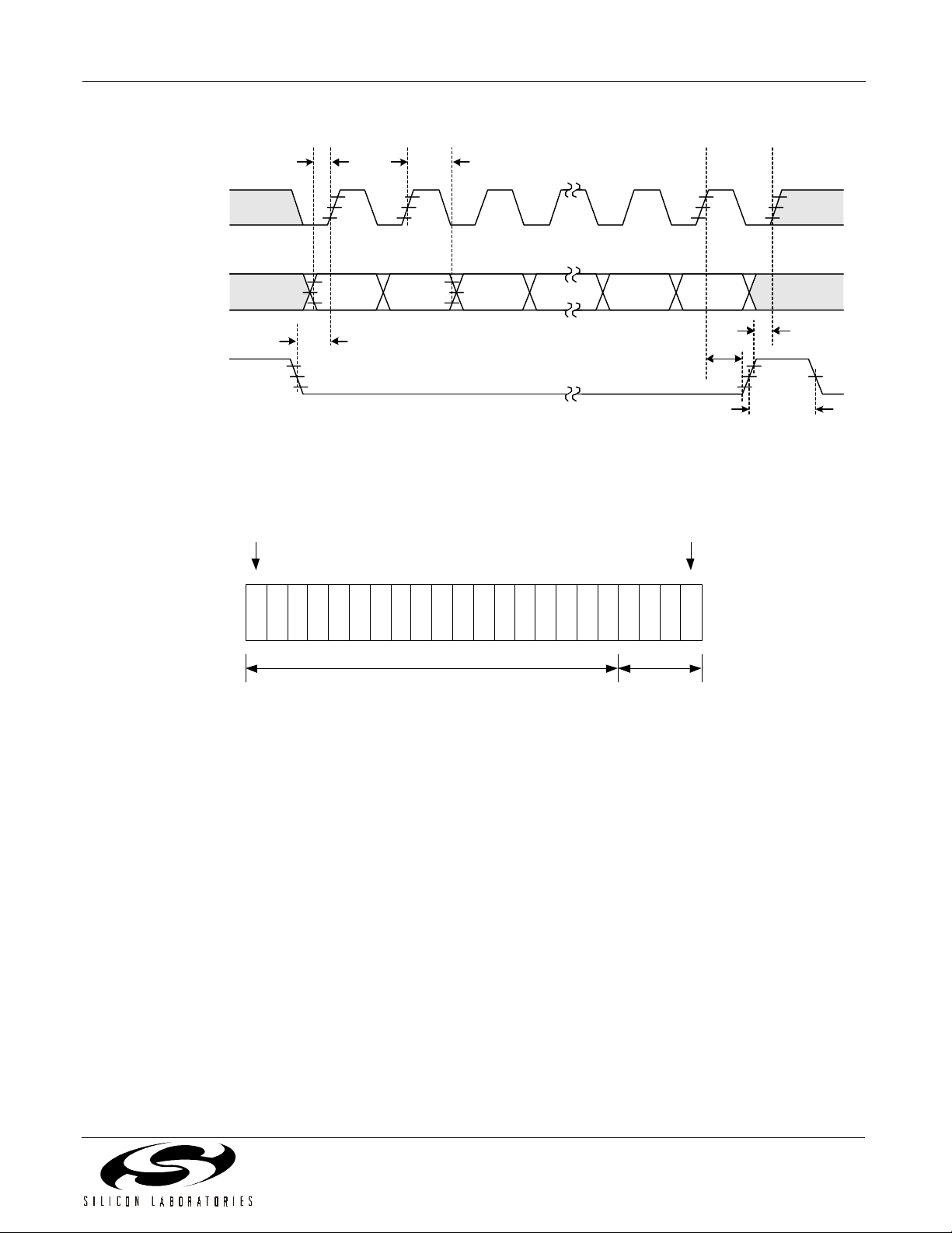
SCLK
80%
50%
20%
t
r
t
f
t
h
t
l
t
clk
Figure 1. SCLK Timing Diagram
6 Rev. 1.1
Page 7
Si4133
SCLK
SDATA
SENB
First bit
cloc ked in
t
su
D17 D16 D15 A1 A0
t
en1
t
hold
Figure 2. Serial Interface Timing Diagram
Last bit
cloc ked in
t
en3
t
en2
t
w
D17D16D15D14D13D12D11D10D9D8D7D6D5D4D3D2D1D0A3A2A1A
data
field
address
field
Figure 3. Serial Word Format
0
Rev. 1.1 7
Page 8

Si4133
Table 5. RF and IF Synthesizer Characteristics
(VDD = 2.7 to 3.6 V, TA = –40 to 85°C)
Parameter
1
XIN Input Frequency f
Reference Amplifier Sensitivity V
Symbol Test Condition Min Typ Max Unit
REF
REF
2—26MHz
0.5 — VDD
V
P-P
+0.3 V
Phase Detector Update Frequency f
RF1 VCO Center Frequency Range f
RF1 VCO Tuning Range
2
φ
CEN
f
= f
/R 0.010 — 1.0 MHz
REF
φ
Extended frequency
947 — 1720 MHz
1850 — 2050 MHz
operation
RF2 VCO Center Frequency Range f
RF Tuning Range from f
CEN
IF VCO Center Frequency Range f
CEN
CEN
Note: L
±10% –5 — 5 %
EXT
789 — 1429 MHz
526 — 952 MHz
IFOUT Tuning Range with IFDIV 62.5 — 1000 MHz
IFOUT Tuning Range from f
CEN
Note: L
±10% –5 — 5 %
EXT
RF1 VCO Pushing Open loop — 500 — kHz/V
RF2 VCO Pushing — 400 — kHz/V
IF VCO Pushing — 300 — kHz/V
RF1 VCO Pulling VSWR = 2:1, all
RF2 VCO Pulling — 300 — kHz
phases, open loop
— 900 — MHz
IF VCO Pulling — 100 — kHz
RF1 Phase Noise 1 MHz offset — –132 — dBc/Hz
RF1 Integrated Phase Error 10 Hz to 100 kHz — 0.9 — degrees
rms
RF2 Phase Noise 1 MHz offset — –134 — dBc/Hz
RF2 Integrated Phase Error 10 Hz to 100 kHz — 0.7 — degrees
rms
IF Phase Noise 100 kHz offset — –117 — dBc/Hz
IF Integrated Phase Error 100 Hz to 100 kHz — 0.4 — degrees
rms
Notes:
= 200 kHz, RF1 = 1.6 GHz, RF2 = 1.2 GHz, IFOUT = 550 MHz, LPWR = 0, for all parameters unless otherwise noted.
1. f
φ
2. Extended frequency operation only. V
RFLB pins. See Application Note 41 for more details on the Si4133 extended frequency operation.
3. From power up request (PWDNB↑ or SENB↑ during a write of 1 to bits PDIB and PDRB in Register 2) to RF and IF
synthesizers ready (settled to within 0.1 ppm frequency error).
4. From power down request (PWDNB↓, or SENB↑ during a write of 0 to bits PDIB and PDRB in Register 2) to supply
current equal to I
PWDN
.
≥ 3.0 V, MLP only, VCO Tuning Range fixed by directly shorting the RFLA and
DD
8 Rev. 1.1
Page 9
Table 5. RF and IF Synthesizer Characteristics (Continued)
(VDD = 2.7 to 3.6 V, TA = –40 to 85°C)
Si4133
Parameter
1
Symbol Test Condition Min Typ Max Unit
RF1 Harmonic Suppression Second Harmonic — –26 –20 dBc
RF2 Harmonic Suppression — –26 –20 dBc
IF Harmonic Suppression — –26 –20 dBc
RFOUT Power Level Z
RFOUT Power Level
2
ZL = 50 Ω, RF1 active,
= 50 Ω –8 –3 1 dBm
L
–14 –7 1 dBm
Extended frequency
operation
IFOUT Power Level Z
= 50 Ω –8 –4 0 dBm
L
RF1 Output Reference Spurs Offset = 200 kHz — –65 — dBc
Offset = 400 kHz — –71 — dBc
Offset = 600 kHz — –75 — dBc
RF2 Output Reference Spurs Offset = 200 kHz — –65 — dBc
Offset = 400 kHz — –71 — dBc
Offset = 600 kHz — –75 — dBc
Power Up Request to Synthesizer
3
Ready
Time
t
pup
Figures 4, 5 — 40/f
50/f
φ
φ
Power Down Request to Synthesizer
4
Off
Time
Notes:
1. f
= 200 kHz, RF1 = 1.6 GHz, RF2 = 1.2 GHz, IFOUT = 550 MHz, LPWR = 0, for all parameters unless otherwise noted.
φ
2. Extended frequency operation only. V
RFLB pins. See Application Note 41 for more details on the Si4133 extended frequency operation.
3. From power up request (PWDNB↑ or SENB↑ during a write of 1 to bits PDIB and PDRB in Register 2) to RF and IF
synthesizers ready (settled to within 0.1 ppm frequency error).
4. From power down request (PWDNB↓, or SENB↑ during a write of 0 to bits PDIB and PDRB in Register 2) to supply
current equal to I
PWDN
.
t
pdn
≥ 3.0 V, MLP only, VCO Tuning Range fixed by directly shorting the RFLA and
DD
Figures 4, 5 — — 100 ns
Rev. 1.1 9
Page 10
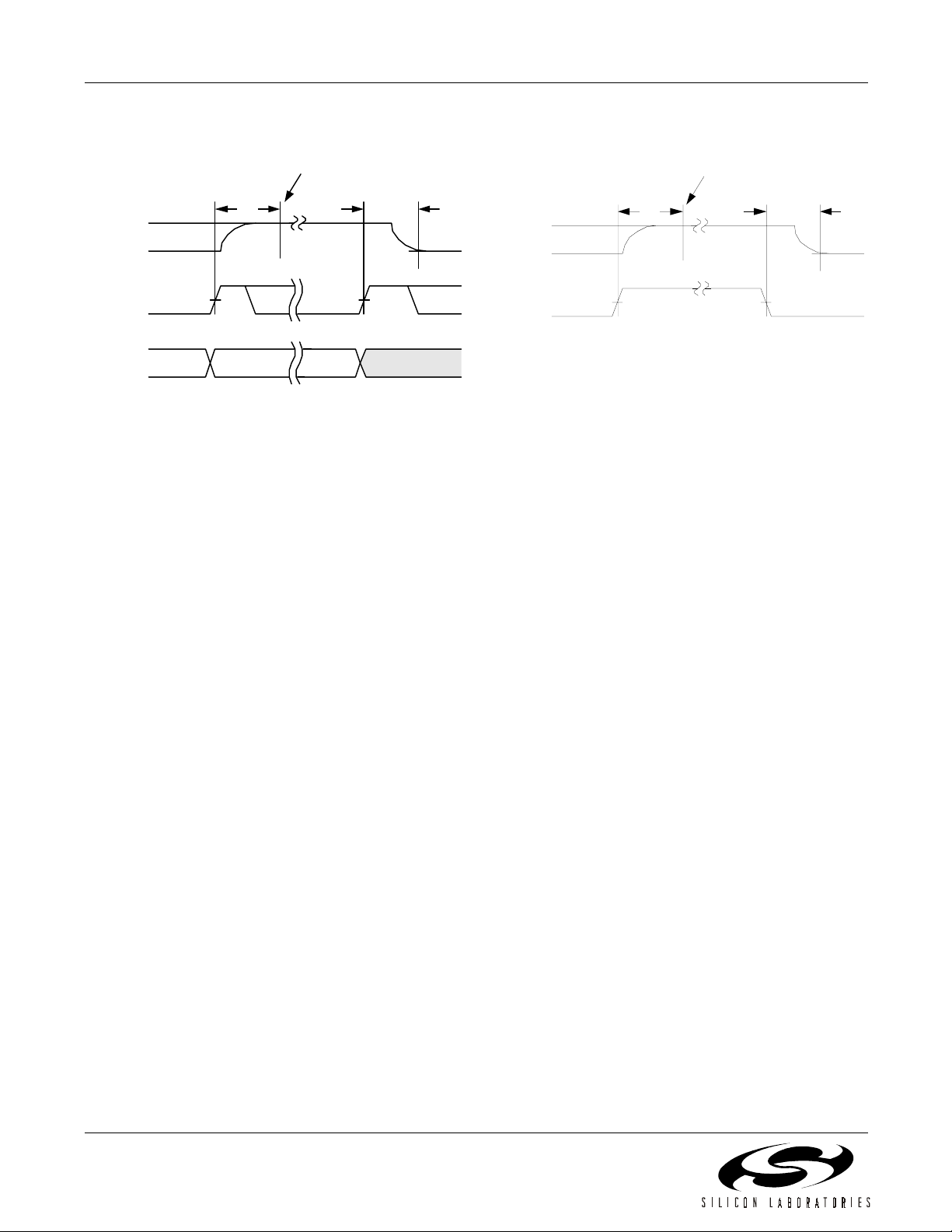
Si4133
RF and IF synthes iz er s settled to
w ithi n 0.1 ppm frequency error.
t
pup
I
PWD N
I
T
SENB
SDATA
PDIB = 1
PDRB = 1
PDIB = 0
PDRB = 0
Figure 4. Software Power Management
Timing Diagram
RF and IF synthes ize r s settled to
w ithi n 0.1 ppm frequency error.
t
pdn
I
PWD N
I
T
t
pup
t
pdn
PWDNB
Figure 5. Hardware Power Management
Timing Diagram
10 Rev. 1.1
Page 11
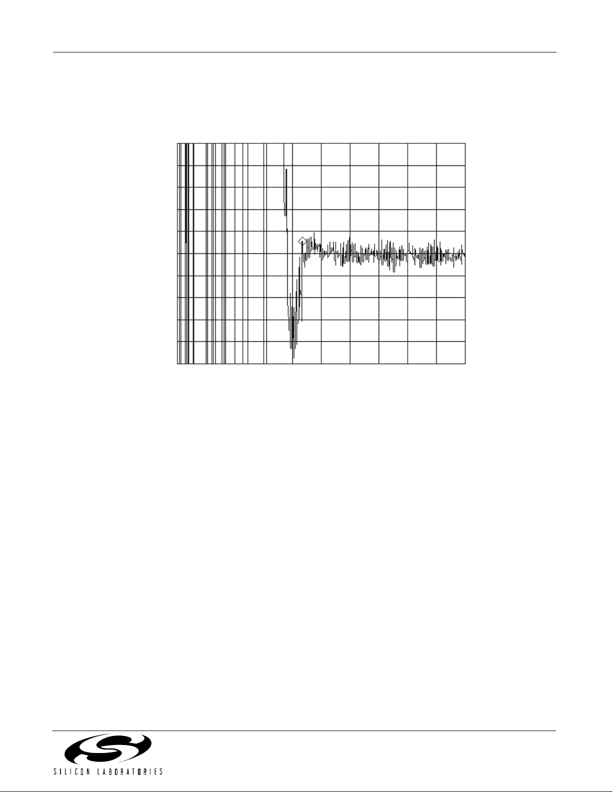
TRACE A: Ch1 FM Main Time
A Marker 174.04471
1.424
kHz
Real
160
Hz
/div
us
Si4133
711.00 Hz
176
Hz
Start: 0 s
Stop: 399.6003996 us
Figure 6. Typical Transient Response RF1 at 1.6 GHz
with 200 kHz Phase Detector Update Frequency
Rev. 1.1 11
Page 12

Si4133
−60
−70
−80
−90
−100
−110
Phase Noise (dBc/Hz)
−120
−130
−140
2
10
3
10
Offset Frequency (Hz)
4
10
10
Figure 7. Typical RF1 Phase Noise at 1.6 GHz
with 200 kHz Phase Detector Update Frequency
5
6
10
Figure 8. Typical RF1 Spurious Response at 1.6 GHz
with 200 kHz Phase Detector Update Frequency
12 Rev. 1.1
Page 13

−60
−70
−80
−90
−100
−110
Phase Noise (dBc/Hz)
−120
−130
Si4133
−140
2
10
3
10
Offset Frequency (Hz)
4
10
10
Figure 9. Typical RF2 Phase Noise at 1.2 GHz
with 200 kHz Phase Detector Update Frequency
5
6
10
Figure 10. Typical RF2 Spurious Response at 1.2 GHz
with 200 kHz Phase Detector Update Frequency
Rev. 1.1 13
Page 14

Si4133
−70
−80
−90
−100
−110
−120
Phase Noise (dBc/Hz)
−130
−140
−150
2
10
3
10
Offset Frequency (Hz)
4
10
10
Figure 11. Typical IF Phase Noise at 550 MHz
with 200 kHz Phase Detector Update Frequency
5
6
10
Figure 12. IF Spurious Response at 550 MHz
with 200 kHz Phase Detector Update Frequency
14 Rev. 1.1
Page 15

Printed Trace
Induc to rs
RFOUT
From
System
Controller
560pF 2n H
Si4133-BT
1
SCLK
2
SDATA
3
GNDR
4
RFLD
5
RFLC
6
GNDR
7
RFLB
8
RFLA
9
GNDR
10
GNDR
11
0.022µF
* Add 30 Ω
V
Ω series resistance if using IF output divide values 2, 4, or 8.
ΩΩ
RFOUT
DD
12
VDDR
SENB
IFOU T
GNDD
VDDD
GNDD
PWDNB
AUXOU T
VDDI
GNDI
IFLB
IFLA
XIN
Si4133
V
DD
30 Ω
Ω *
24
23
22
21
20
19
18
17
16
15
14
13
ΩΩ
F
µ
0.022
560pF10nH
IFOU T
Printed Trace
Inductor or
Chip Inductor
0.022µF
V
DD
560pF
External Clock
PWDNB
AUXOU T
From
System
Controller
Printed Trace
Inductors
PWDNB
Figure 13. Typical Application Circuit: Si4133-BT
V
DD
30 Ω
Ω *
ΩΩ
µ
0.022
* Add 30
F
22232425262728
SDATA
GNDR
F
µ
SCLK
Si4133-BM
RFOUT
1
2
3
4
5
6
7
GNDR
GNDR
RFLD
RFLC
GNDR
RFLB
RFLA
GNDR
GNDR
8 9 10 11 12 13 14
V
DD
0.022
ΩΩΩΩ
series resistance if using IF output divide values 2, 4, or 8.
SENB
VDDR
VDDI
AUXOUT
GNDI
IFOUT
PWDNB
GNDD
VDDD
GNDD
GNDD
GNDI
IFLB
IFLA
XIN
21
20
19
18
17
16
15
10nH
V
DD
2nH
560pF
Printed Trace
Inductor or
Chip Ind u c tor
0.022µF
560pF
560pF
IFOU T
External Clock
AUXOUT
RFOUT
Figure 14. Typical Application Circuit : Si4133-BM
Rev. 1.1 15
Page 16

Si4133
Functional Description
The Si4133 is a monolithic integrated circuit that
performs IF and dual-band RF synthesis for wireless
communications applications. This integrated circuit
(IC), with minimal external com ponents, completes the
frequency synthesis function necessary for RF
communicatio ns sy s tems .
The Si4133 has three complete phase-locked loops
(PLLs) with integrated voltage-controlled oscillators
(VCOs). The low ph ase noise of the VCOs mak es the
Si4133 suitable for use in demanding wireless
communications applications. Phase detectors, loop
filters, and referenc e and output freq uency dividers a re
integrated. The IC is pr ogrammed through a three- wire
serial interface.
Two PLLs are provided for dual-band RF synthesis.
These RF PLLs are mult iplex ed so that only one P LL is
active at a given time (as determi ned by the setting of
an internal register). The active PLL is the last one
written. The center frequency of the VCO in each PLL is
set by the value of an external induc tan ce. Inac cu raci es
in these inductances are compensated for by the selftuning algorithm. Th e algorithm is run following power up or following a change in the programmed output
frequency.
Each RF PLL, when active, can adjust the RF output
frequency by ±5% of its VCO’s center frequency.
Because the two VCOs can be set to have widely
separated center frequencies, the RF output can be
programmed to serv ice t wo w idely s epar ated freq uency
bands by simply programming the corresponding NDivider. One RF VCO is optimized to have its center
frequency set between 947 MHz and 1.72 GHz, while
the second RF VCO is optimized to have its center
frequency set between 789 MHz and 1.429 GHz.
One PLL is provided for IF frequency synthesis. The
center frequency of this circuit’s VCO is set by
connection of an external inductance. The PLL can
adjust the IF output frequency by ±5% of the VCO
center frequency. Inaccuracies in the value of the
external inductance are compensated for by the
Si4133’s proprietary self-tuning algorithm. This
algorithm is initia ted each time the PLL is powered-up
(by either the PW DNB pin or by software) and /or each
time a new output frequency is programmed.
The IF VCO can have its center frequency set as low as
526 MHz and as high as 952 MHz. An IF output divider
is provided to divi de down the IF output freq uencies, if
needed. The divider is programmable, capable of
dividing by 1, 2, 4, or 8.
The unique PLL architecture used in the Si4133
produces settling (lock) times that are comparable in
speed to fractional- N architec tures with out suffering the
high phase noise or spurious modulation effects often
associated with those designs.
Serial Inte rface
A timing diagram for the serial interface is shown in
Figure 2 on page 7. Figure 3 on page 7 shows the
format of the serial word.
The Si4133 is programmed serially with 22-bit words
comprised of 18-bit da ta fields and 4-bit addr ess fields.
When the serial interface is enabled (i.e., when SENB is
low) data and address bits on the SDATA pin are
clocked into an internal s hift register on the risin g edge
of SCLK. Data in the shift re gis ter i s t hen trans fer red o n
the rising edge of SENB into the internal data register
addressed in the address field. The serial interface is
disabled when SENB is high.
Table 12 on page 21 summarizes the data register
functions and addr esses. The internal s hift register will
ignore any leading bits before the 22 required bits.
Setting the VCO Center Frequencies
The PLLs can adju st the IF and RF outp ut frequencies
±5% of the center frequencies of their VCOs. Each
center frequency is established by the value of an
external inductance connected to the respective VCO.
Manufacturing tolerances of ±10% for the external
inductances are acceptable. The Si4133 will
compensate for inaccuracies in each inductance by
executing a self-tu ning algorithm following PLL powerup or following a change in the programmed output
frequency.
Because the total tank inductance is in the low nH
range, the inductance of the package needs to be
considered in determining the correct external
inductance. The total inductance (L
each VCO is the su m of the externa l inductanc e (L
and the package i nductance (L
nominal capacitance (C
inductance, and the center frequency is as follows:
NOM
PKG
) in parallel with the total
) presented to
TOT
). Each VCO has a
EXT
)
16 Rev. 1.1
Page 17

Si4133
f
CEN
---------------------------------------------=
2π L
1
⋅
TOTCNOM
or
f
CEN
----------------------------------------------------------------------=
2π L
1
+()C
PKGLEXT
⋅
NOM
Tables 6 and 7 summarize the characteristics of each
VCO.
Table 6. Si4133-BT VCO Characteristics
VCO f
RF1 947 1720 4.3 2.0 0.0 4.6
RF2 789 1429 4.8 2.3 0.3 6.2
IF 526 952 6.5 2.1 2.2 12.0
Range
CEN
(MHz)
Min Max Min Max
C
(pF)
NOM
L
L
PKG
(nH)
EXT
Range
(nH)
Table 7. Si4133-BM VCO Characteristics
VCO f
RF1 947 1720 4.3 1.5 0.5 5.1
RF2 789 1429 4.8 1.5 1.1 7.0
IF 526 952 6.5 1.6 2.7 12.5
Range
CEN
(MHz)
Min Max Min Max
C
L
L
NOM
(pF)
L
PKG
2
L
PKG
2
PKG
(nH)
EXT
Range
(nH)
L
EXT
Figure 15. External Inductance Connection
As a design example , s upp os e th e go al is to s yn the siz e
frequencies in a 25 MHz band between 1120 MHz and
1145 MH z. The center frequency s hould be defined as
midway between the two extremes, or 1132.5 MHz. The
PLL will be able to adjust the VCO output frequency
±5% of the center frequency, or ±56.6 MHz of
1132.5 MHz (i.e., from approximately 1076 MHz to
1189 MHz). The RF2 VCO has a C
of 4.8pF. A
NOM
4.1 nH induc tance (correct to two di gits) in parallel wit h
this capacitance will yield the desired c enter frequen cy.
An external inducta nce of 1.8 nH sh ould be connected
between RFLC and RFLD a s shown in Figure 15. This ,
in addition to 2.3 nH of package inductance, will present
the correct total inductance to the VCO. In
manufacturing, the extern al inductance can vary ±10%
of its nominal value and the Si 4133 will correct for the
variation with the self-tuning algorithm.
For more information on designing the external trace
inductors, refer to Application Note 31.
Extended Frequency Operation
The Si4133 may operate at an extended frequency
range of 1850 MHz to 2050 MHz by connecting the
RFLA and RFLB pins directly. For information on
configuring the Si4133 for extended frequency
operation, refer to Application Note 41.
Self-Tuning Algorithm
The self-tuning algorithm is initiated immediately
following power-up of a PLL or, if the PLL is already
powered, following a c hange in its programmed o utput
frequency. This algorithm attempts t o tune the VCO so
that its free-running frequency is near the desired output
frequency. In doing so, the algorithm will compensate
for manufacturing tolerance errors in the value of the
external inductance conn ected to the VCO. It will also
reduce the frequency error for which the PLL must
correct to get the prec ise desi red ou tput fr equency. The
self-tuning algorith m will leave the VCO oscillating at a
frequency in error by somewhat less than 1% of the
desired output frequency.
After self-tuning, the PLL controls the VCO oscillation
frequency. The PLL will complete frequency locking,
eliminating any remaining frequency error. Thereafter, it
will maintain frequency-lock, compensating for effects
caused by temperature and supply voltage variations.
The Si4133’s self-tuning algorit hm will compensate for
component value errors at any temperature within the
specified temperature r ange. Howeve r, the ability of the
PLL to compensate for drift in component values that
occur after self-tuning is limited. For external
inductances with temperature coefficients around
±150 ppm/
changes in temperature of approximately ±30
o
C, the PLL will be able to maintain lock for
o
C.
Rev. 1.1 17
Page 18

Si4133
Applications where the PLL is regularly powered-down
or the frequency is periodic ally re program med min imize
or eliminate the potential effects of temperature drift
because the VCO is re-tuned in either case. In
applications where the ambient temperature can drift
substantially after self-tuning, it may be necessary to
monitor the lock-detect bar (LDETB) signal on the
AUXOUT pin to determine whether a PLL is about to
run out of locking capability. (See “Auxiliary Output
(AUXOUT)” for how to select LDETB.) The LDETB
signal will be low after self-tuning has completed but will
rise when either the IF or RF PLL nears the limit of its
compensation range. (LDETB will also be high when
either PLL is executin g the self-tuning algorithm.) The
output frequency wi ll still be locked when LDETB goes
high, but the PLL will eventually lose lock if the
temperature continues to drift in the same direction.
Therefore, if LDETB goes high both the IF and RF PLLs
should promptly be re-tu ned by initiating th e self-tuning
algorithm.
Output Frequencies
The IF and RF output frequencies are set by
programming the R- and N-Divi der registers. Eac h PLL
has its own R and N registers so that each can be
programmed independ ently. Programming either the Ror N-Divider register for RF1 or RF2 automatically
selects the associated output.
The reference frequ ency on the XIN pin is divided b y R
and this signal is inpu t to the P LL’s phase detector. The
other input to the phase detector is the PLL’s VCO
output frequency divi ded by N. The PLL acts to make
these frequencies equal. That is, after an initial transient
f
OUT
------------
or
f
OUT
The R values are set by programming the RF1 RDivider register (Re gister 6), the RF2
(Register 7) and the IF R-Divider register (Register 8).
The N values are set by programming the RF1 NDivider register (Regi ster 3), the RF2 N-Divider r egister
(Register 4), and the IF N-Divider register (Register 5).
Each N-Divider is impl emented as a conventional high
speed divider. That is, it consists of a dual-modulus
prescaler, a swallow counter, and a lower speed
synchronous counter. However, the control of these
sub-circuits is handled automatically. Only the
appropriate N value should be programmed.
f
REF
-----------=
N
R
N
----
⋅=
f
REF
R
R-Divider register
PLL Loop Dynamics
The transient resp onse for each PLL is deter mined by
its phase detector u pdate rate f
the phase detector gain programmed for each RF1,
RF2, or IF synthesizer. (See Register 1.) Four different
settings for the phase detector gain are available for
each PLL. The highest gain is pr ogrammed by setting
the two phase detector gain bits to 00, and the lowest by
setting the bits to 11. The values of the availabl e gains ,
relative to the highest gain, are as follows:
Table 8. Gain Values (Register 1)
KP Bits
00 1
01 1/2
10 1/4
11 1/8
The gain value bits ca n be automatically set by settin g
the Auto K
bit (bit 2) in the M ain Configu ration reg ister
P
to 1. In setting this bit, the gain va lues will be opti mized
for a given value of N. In general, a higher phase
detector gain will decrease in-band phase noise and
increase the speed of the PLL transient until the point at
which stability begins to be compromised. The optimal
gain depends on N. Table 9 lists recom mended s ettings
for different values of N. These are the settings used
when the Auto K
bit is set.
P
Table 9. Optimal KP Settings
N
≤2047 00 00 00
2048 to 4095 00 00 01
4096 to 8191 00 01 10
8192 to 16383 01 10 11
16384 to 32767 10 11 11
≥32768 11 11 11
The VCO gain and loop filter characteristics are not
programmable.
The settling time for the PLL is directly proportional to its
phase detector update period T
typical transient respo nse is shown in Figu re 6 on page
11. During the first 13 update periods the Si4133
executes the self- tuning algorithm. Thereafter the PL L
K
RF1
P1
<1:0>
(equal to f
φ
REF
/R) and
Relative P.D.
Gain
RF2
KP2<3:2>IFKPI<5:4>
(Tφ equals 1/fφ). A
φ
18 Rev. 1.1
Page 19

controls the output frequency. Because of the unique
architecture of the Si4133 PLLs, the time required to
settle the output frequency to 0.1 ppm error is only
about 25 update periods. Thus, the total time after
power-up or a change in programmed frequency until
the synthesized frequency is well settled—including
time for self-tuning—is around 40 update periods.
Note: The settling time analysis holds for RF1 fφ ≤ 500 kHz.
For RF1 f
> 500 kHz, the settling time is larger.
φ
RF and IF Outputs
The RFOUT and IFOUT pins are driven by amplifiers
that buffer the RF VC Os and IF VCO, respecti vely. The
RF output amplifier receives its input from either the
RF1 or RF2 VCO, depending upon which R- or NDivider register was last written. For example,
programming the N-Divider register for RF1
automatically selects the RF1 VCO output.
Figures 13 and 14 show application diagrams for the
Si4133. The RF output signa l must be A C coupled to its
load through a capacitor. An external inductance
between the RFOUT pin a nd the AC co upling c apacitor
is required as part of an output matching network to
maximize power delivered to the load. This 2 nH
inductance may be real ized wi th a PC boa rd trace. Th e
network is made to provide an adequate match to an
external 50 Ω load for b oth the RF1 and RF2 freq uency
bands. The matching network also filters the output
signal to reduce harmonic distortion.
The IFOUT pin must also be AC coupled to its load
through a capacitor. The IF output level is dependent
upon the load. Figure 18 on page 20 displays the output
level versus load resistance for a variety of output
frequencies. For resis tive loads greater than 500 Ω the
output level saturates and the bias currents in the IF
output amplifier are higher than they need to be. The
LPWR bit in the Main Configuration register (Register 0)
can be set to 1 to reduce the bias currents and therefore
reduce the power dissipated by the IF amplifier. For
loads less than 500 Ω, LPWR should be set to 0 to
maximize the output level.
For IF frequencies greater than 500 MHz, a matching
network is required in order to dr ive a 50 Ω load. Se e
Figure 16 below. The value of L
determined from Table 10.
Table 10. L
MATCH
Frequency L
Values
MATCH
500–600 MHz 40 nH
600–800 MHz 27 nH
800MHz–1GHz 18nH
MATCH
can be
Si4133
560 pF
IFO U T
L
MATCH
Ω
50
Figure 16. IF Frequencies > 500 MHz
For frequencies les s than 500 MHz, the IF output b uffer
can directly drive a 200 Ω resistive l oad or higher. For
resistive loads greater than 500 Ω (f < 500 MHz) the
LPWR bit can be set to reduc e the po wer cons umed by
the IF output buffer. See Figure 17 below.
>500 pF
IFO U T
Ω
>200
Figure 17. IF Frequencies < 500 MHz
Reference Frequency Amplifier
The Si4133 provides a refer ence frequency amp lifier. If
the driving signal has C MOS level s it c an be conne cted
directly to the XIN pin. Otherwise, the reference
frequency signal should be AC coupl ed to the XIN pin
through a 560 pF capacitor.
Power Down Modes
Table 11 summarizes the power down functionality. The
Si4133 can be powered down by taking the PWDNB pin
low or by setting bits in the Power Down register
(Register 2). When the PWDNB pin is low, the Si4133 will
be powered down regardless of the Power Down register
settings. When the PWDNB pin is high, power
management is under control of the Power Down register
bits.
The IF and RF sections of the Si4133 circuitry can be
individually powered down by setting the Power Down
register bits P DIB and PDRB low, respectivel y. Note that
the reference frequency amplifier will also be po wered up if
either the PDRB and PDIB bits are high. Also, setting the
AUTOPDB bit to 1 in the Main Configuration register
(Register 0) is equivalent to setting both bits in the Power
Down register to 1.
The serial interface remains available and can be written in
all power down modes.
Rev. 1.1 19
Page 20

Si4133
Auxiliary Output (AUXOUT)
The signal appearing on AUXOUT is selected by setting
the AUXSEL bits in the Main Configuration register
(Register 0).
Table 11. Power Down Configuration
PWDNB Pin AUTOPDB PDIB PDRB IF Circuitry
PWDNB = 0
PWDNB = 1
450
XXXOFFOFF
000OFFOFF
001OFFON
010ONOFF
011ONON
1xxONON
The LDETB signal can be selected by setting the AUXSEL
bits to 11. This signal can be used to indica te tha t t he IF or
RF PLL is about to lose lock due to excessive ambient
temperature drift an d should be re- tuned.
RF
Circuitry
400
350
300
250
200
Output Voltage (mVrms)
150
100
50
0
LPWR=0
0 200 400 600 800 1000 1200
LPWR=1
Load Resistance (ΩΩΩΩ)
Figure 18. Typical IF Output Voltage vs. Load Resistance at 550 MHz
20 Rev. 1.1
Page 21

Si4133
Control Registers
T able 12. Register Summary
Register Name Bit 17Bit 16Bit 15Bit 14Bit 13Bit 12Bit 11Bit 10Bit 9Bit 8Bit 7Bit 6Bit 5Bit 4Bit3Bit 2Bit 1Bit
0
0
Main
Configuration
000 0
AUXSEL
[1:0]
IFDIV
[1:0]
0000
LPWR
AUTO
AUTO
0
PDB
RF
K
PWR
P
0
1
2
3
4
5
6
7
8
Phase
Detector Gain
Power Down
RF1
N-Divider
RF2
N-Divider
IF N-Divider
RF1
R-Divider
RF2
R-Divider
IF R-Divider
0000 0 0000000 K
0000 0 0000000 0 0 0 0
[17:0]
N
RF1
0N
00 N
000 0 0 R
000 0 0 R
000 0 0 R
RF2
[16:0]
[15:0]
IF
RF1
RF2
IF
[12:0]
[12:0]
[12:0]
PI
[1:0]
[1:0]
K
P2
[1:0]
K
P1
PDIB PDRB
9 Reserved
.
.
.
15 Reserved
Note: Registers 9–15 are reserved. Writes to these registers may result in unpredictable behavior. Any register not listed here
is reserved and should not be written.
Rev. 1.1 21
Page 22

Si4133
Register 0. Main Configuration Address Field = A[3:0] = 0000
Bit D17 D16 D15 D14 D13 D12 D11 D10 D9 D8 D7 D6 D5 D4 D3 D2 D1 D0
Name 0000AUXSEL
[1:0]
IFDIV
[1:0]
0000
LPWR
0
Bit Name Function
17:14 Reserved Program to zero.
13:12 AUXSEL
[1:0]
Auxiliary Output Pin Definition.
00 = Reserved.
01 = Force output low.
10 = Reserved.
11 = Lock Detect—LDETB.
11:10 IFDIV
[1:0]
IF Output Divider.
00 = IFOUT = IFVCO Frequency
01 = IFOUT = IFVCO Frequency/2
10 = IFOUT = IFVCO Frequency/4
11 = IFOUT = IFVCO Frequency/8
9:6 Reserved Program to zero.
5LPWROutput Power-Level Settings for IF Synthesizer Circuit.
0 = R
1 = R
< 500 Ω—normal power mode.
LOAD
≥ 500 Ω—low power mode.
LOAD
4 Reserved Program to zero.
AUTO
PDB
AUTO
K
P
RF
PWR
0
3 AUTOPDB Auto Power Down.
0 = Software powerdown is controlled by Register 2.
1 = Equivalent to setting all bits in Register 2 = 1.
2AUTOK
P
Auto KP Setting.
0 = K
s are controlled by Register 1.
P
s are set according to Table 9 on page 18.
1 = K
P
1 RFPWR Program to zero. (Used for extended frequency operation. See AN41 for
more information.)
0 Reserved Program to zero.
22 Rev. 1.1
Page 23

Si4133
Register 1. Phase Detector Gain Address Field (A[3:0]) = 0001
Bit D17D16D15D14D13D12D11D10D9D8D7D6D5D4D3D2D1D0
Name 000000000000K
PI
[1:0]
[1:0]
K
P2
[1:0]
K
P1
Bit Name Function
17:6 Reserved Program to zero.
5:4 K
PI
[1:0]
IF Phase Detector Gain Constant.*
N Value K
PI
<2048 = 00
2048–4095 = 01
4096–8191 = 10
>8191 = 11
3:2 K
P2
[1:0]
RF2 Phase Detector Gain Constant.*
N Value K
P2
<4096 = 00
4096–8191 = 01
8192–16383 = 10
>16383 = 11
1:0 K
P1
[1:0]
RF1 Phase Detector Gain Constant.*
N Value K
P1
<8192 = 00
8192–16383 = 01
16384–32767 = 10
>32767 = 11
*Note: When AUTOKP = 1, these bits do not need to be programmed. When AUTOKP = 0, use these recommended values
for programming Phase De tector Gain.
Rev. 1.1 23
Page 24

Si4133
Register 2. Power Down Address Field (A[3:0]) = 0010
Bit D17 D16 D15 D14 D13 D12 D11 D10 D9 D8 D7 D6 D5 D4 D3 D2 D1 D0
Name 000000000000000 0
PDIB PDRB
Bit Name Function
17:2 Reserved Program to 0.
1PDIBPower Down IF Synthesizer.
0 = IF synthesizer powered down.
1 = IF synthesizer on.
0 PDRB Power Down RF Synthesizer.
0 = RF synthesizer powered down.
1 = RF synthesizer on.
Note: Enabling any PLL with PDIB or PDRB will automatically power on the reference amplifier.
Register 3. RF1 N-Divider Address Field (A[3:0]) = 0011
BitD17D16D15D14D13D12D11D10D9D8D7D6D5D4D3D2D1D0
Name N
RF1
[17:0]
Bit Name Function
17:0 N
RF1
[17:0]
N-Divider for RF1 Synthesizer.
Register 4. RF2 N-Divider Address Field = A[3:0] = 0100
Bit D17D16D15D14D13D12D11D10D9D8D7D6D5D4D3D2D1D0
Name 0N
RF2
[16:0]
Bit Name Function
17 Reserved Program to 0.
16:0 N
24 Rev. 1.1
RF2
[16:0]
N-Divider for RF2 Synthesizer.
Page 25

Si4133
Register 5. IF N-Divider Address Field (A[3:0]) = 0101
Bit D17D16D15D14D13D12D11D10D9D8D7D6D5D4D3D2D1D0
Name 00 N
[15:0]
IF
Bit Name Function
17:16 Reserved Program to zero.
15:0 N
[15:0]
IF
N-Divider for IF Synthesizer.
Register 6. RF1 R-Divider Address Field (A[3:0]) = 0110
Bit D17D16D15D14D13D12D11D10D9D8D7D6D5D4D3D2D1D0
Name 00000 R
RF1
[12:0]
Name Function
17:13 Reserved Program to zero.
12:0 R
RF1
[12:0]
R-Divider for RF1 Synthesizer.
can be any value from 7 to 8189 if KP1 = 00
R
RF1
8 to 8189 if K
10 to 8189 if K
14 to 8189 if K
P1
P1
P1
= 01
= 10
= 11
Register 7. RF2 R-Divider Address Field (A[3:0]) = 0111
Bit D17D16D15D14D13D12D11D10D9D8D7D6D5D4D3D2D1D0
Name 00000 R
RF2
[12:0]
Bit Name Function
17:13 Reserved Program to zero.
12:0 R
RF2
[12:0]
R-Divider for RF2 Synthesizer.
R
can be any value from 7 to 8189 if KP2 = 00
RF2
8 to 8189 if K
10 to 8189 if K
14 to 8189 if K
Rev. 1.1 25
P2
P2
P2
= 01
= 10
= 11
Page 26

Si4133
Register 8. IF R-Divider Address Field (A[3:0]) = 1000
Bit D17D16D15D14D13D12D11D10D9D8D7D6D5D4D3D2D1D0
Name 00000 R
[12:0]
IF
Bit Name Function
17:13 Reserved Program to zero.
12:0 R
[12:0]
IF
R-Divider for IF Synthesizer.
can be any value from 7 to 8189 if KP1 = 00
R
IF
8 to 8189 if K
10 to 8189 if K
14 to 8189 if K
P1
P1
P1
= 01
= 10
= 11
26 Rev. 1.1
Page 27

Pin Descriptions: Si4133-BT
Si4133
SCLK
SDATA
GNDR
RFLD
RFLC
GNDR
RFLB
RFLA
GNDR
GNDR
RFOUT
VDDR
124
223
322
421
520
619
718
817
916
10 15
11 14
12 13
SENB
VDDI
IFOUT
GNDI
IFLB
IFLA
GNDD
VDDD
GNDD
XIN
PWDNB
AUXOUT
Pin Number(s) Name Description
1 SCLK Serial cl ock input
2 SDATA Serial data input
3, 6, 9, 10 GNDR Common ground for RF analog circuitry
4, 5 RFLC, RFLD Pins for inductor connection to RF2 VCO
7, 8 RFLA, RFLB Pins for inductor connection to RF1 VCO
11 RFOUT Radio frequency (RF) output of the selected RF VCO
12 VDDR Supply voltage for the RF analog circuitry
13 AUXOUT Auxiliary output
14 PWDNB Power down input pin
15 XIN Reference frequency amplifier input
16, 18 GNDD Common ground for digital circuitry
17 VDDD Supply voltage for digital circuitry
19, 20 IFLA, IFLB Pins for inductor connection to IF VCO
21 GNDI Common ground for IF analog circuitry
22 IFOUT Intermediate frequency (IF) output of the IF VCO
23 VDDI Supply voltage for IF analog circuitry
24 SENB Enable serial port input
Rev. 1.1 27
Page 28

Si4133
Table 13. Pin Descriptions for Si4133 Derivatives—TSSOP
Pin Number Si4133 Si4123 Si4122 Si4113 Si4112
1 SCLK SCLK SCLK SCLK SCLK
2 SDATA SDATA SDATA SDATA SDATA
3 GNDR GNDR GNDR GNDR GNDD
4 RFLD GNDR RFLD RFLD GNDD
5 RFLC GNDR RFLC RFLC GNDD
6 GNDR GNDR GNDR GNDR GNDD
7 RFLB RFLB G NDR RFLB GNDD
8 RFLA RFLA G NDR RFLA GNDD
9 GNDR GNDR GNDR GNDR GNDD
10 GNDR GNDR GNDR GNDR GNDD
11 RFOUT RFOUT RFOUT RFOUT GNDD
12 VDDR VDDR VDDR VDDR VDDD
13 AUXOUT AUXOUT AUXOUT AUXOUT AUXOUT
14 PWDNB PWDNB PWDNB PWDNB PWDNB
15 XIN XIN XIN XIN XIN
16 GNDD GNDD GNDD GNDD GNDD
17 VDDD VDDD VDDD VDDD VDDD
18 GNDD GNDD GNDD GNDD GNDD
19 IFLA IFLA IFLA GNDD IFLA
20 IFLB IFLB IFLB GNDD IFLB
21 GNDI GNDI GNDI GNDD GNDI
22 IFOUT IFOUT IFOUT GNDD IFOUT
23 VDDI VDDI VDDI VDDD VDDI
24 SENB SENB SENB SENB SENB
28 Rev. 1.1
Page 29

Pin Descriptions: Si4133-BM
Si4133
SCLK
SDATA
GNDR
VDDI
GNDI
IFOUT
28 27 26 25 24 23
GNDR
RFLD
RFLC
GNDR GNDD
RFLB
RFLA
GNDR
1
2
3
4
5
6
7
8 9 10 11 12 13 14
GNDR
GNDR
VDDR SENB
RFOUT
AUXOUT
22
GNDI
21
IFLB
20
IFLA
19
18
VDDD
17
GNDD
16
XIN
15
GNDD
PWDNB
Pin Number(s) Name Description
1, 4, 7-9, 28 GNDR Common ground for RF analog circuitry
2, 3 RFLC, RFLD Pins for inductor connection to RF2 VCO
5,6 RFLA, RFLB Pins for inductor connection to RF1 VCO
10 RFOUT Radio frequency (RF) output of the selected RF VCO
11 VDDR Supply voltage for the RF analog circuitry
12 AUXOUT Auxiliary output
13 PWDNB Power down input pin
14, 16, 18 GNDD Common ground for digital circuitry
15 XIN Reference frequency amplifier input
17 VDDD Supply voltage for digital circuitry
19, 20 IFLA, IFLB Pins for inductor connection to IF VCO
21, 22 GNDI Common ground for IF analog circuitry
23 IFOUT Intermediate frequency (IF) output of the IF VCO
24 VDDI Supply voltage for IF analog circuitry
25 SENB Enable serial port input
26 SCLK Serial clock input
27 SDATA Serial data input
Rev. 1.1 29
Page 30

Si4133
Table 14. Pin Descriptions for Si4133 Derivatives—MLP
Pin Number Si4133 Si4123 Si4122 Si4113 Si4112
1 GNDR GNDR GNDR GNDR GNDD
2 RFLD GNDR RFLD RFLD GNDD
3 RFLC GNDR RFLC RFLC GNDD
4 GNDR GNDR GNDR GNDR GNDD
5 RFLB RFLB GNDR RFLB GNDD
6 RFLA RFLA GNDR RFLA GNDD
7 GNDR GNDR GNDR GNDR GNDD
8 GNDR GNDR GNDR GNDR GNDD
9 GNDR GNDR GNDR GNDR GNDD
10 RFOUT RFOUT RFOUT RFOUT GNDD
11 VDDR VDDR VDDR VDDR VDDD
12 AUXOUT AUXOUT AUXOUT AUXOUT AUXOUT
13 PWDNB PWDNB PWDNB PWDNB PWDNB
14 GNDD GNDD GNDD GNDD GNDD
15 XIN XIN XIN XIN XIN
16 GNDD GNDD GNDD GNDD GNDD
17 VDDD VDDD VDDD VDDD VDDD
18 GNDD GNDD GNDD GNDD GNDD
19 IFLA IFLA IFLA GNDD IFLA
20 IFLB IFLB IFLB GNDD IFLB
21 GNDI GNDI GNDI GNDD GNDI
22 GNDI GNDI GNDI GNDD GNDI
23 IFOUT IFOUT IFOUT GNDD IFOUT
24 VDDI VDDI VDDI VDDD VDDI
25 SENB SENB SENB SENB SENB
26 SCLK SCLK SCLK SCLK SCLK
27 SDATA SDATA SDATA SDATA SDATA
28 GNDR GNDR GNDR GNDR GNDD
30 Rev. 1.1
Page 31

Ordering Guide
Si4133
Ordering Part
Description Operating Temperature
Number
o
Si4133-BM RF1/RF2/IF OUT –40 to 85
Si4133-BT RF1/RF2/IF OUT –40 to 85
Si4123-BM RF1/IF OUT –40 to 85
Si4123-BT RF1/IF OUT –40 to 85
Si4122-BM RF2/IF OUT –40 to 85
Si4122-BT RF2/IF OUT –40 to 85
Si4113-BM RF1 OUT –40 to 85
Si4113-BT RF1 OUT –40 to 85
Si4112-BM IF OUT –40 to 85
Si4112-BT IF OUT –40 to 85
C
o
C
o
C
o
C
o
C
o
C
o
C
o
C
o
C
o
C
Si4133 Derivative Devices
The Si4133 performs bo th IF a nd du al -b and RF fre que ncy s y nthe sis. Th e Si4112, Si4113, Si4122, and the Si4123
are derivatives of this device. Table 15 outlines which synthesizers each derivative device features as well as
which pins and registers coincide with each synthesizer.
Table 15. Si4133 Derivatives
Name Synthesizer Pins Registers
Si4112 IF IFLA, IFLB N
Si4113 RF1, RF2 RFLA, RFLB, RFLC, RFLD N
Si4122 RF2, IF RFLC, RFLD, IFLA, IFLB N
Si4123 RF1, IF RFLA, RFLB, IFLA, IFLB N
Si4133 RF1, RF2, IF RFLA, RFLB, RFLC, RFLD,
N
IFLA, IFLB
, RIF, PDIB, IFDIV , LPWR, AUTOPDB = 0,
IF
PDRB = 0
, N
, R
, R
RF1
RF2
RF1
, PDRB, AUTOPDB = 0,
RF2
PDIB = 0
, R
RF2
RF1
RF1
, PDRB, NIF, RIF, PDIB, IFDIV, LPWR
RF2
, R
, PDRB, NIF, RIF, PDIB, IFDIV, LPWR
RF1
, N
, R
, R
RF2
RF1
, PDRB, NIF, RIF, PDIB,
RF2
IFDIV, LPWR
Rev. 1.1 31
Page 32

Si4133
Package Outline: Si4133-BT
2
θ
S
E1 E
1
θ
e
D
A2
A
b
A1
R1
R
L
L1
3
θ
Figure 19. 24-pin Thin Small Shrink Outline Package (TSSOP)
Table 16. Package Diagram Dimensions
Symbol Millimeters
Min Nom Max
A — 1.10 1.20
A1 0.05 — 0.15
A2 0.80 1.00 1.05
b0.19—0.30
c0.09—0.20
D 7.70 7.80 7.90
e0.65 BSC
E6.40 BSC
E1 4.30 4.40 4.50
L 0.45 0.60 0.75
L1 1.00 REF
R0.09 — —
R1 0.09 — —
S0.20— —
θ10 —8
θ2 12 REF
θ3 12 REF
c
32 Rev. 1.1
Page 33

Package Outline: Si4133-BM
Si4133
Figure 20. 28-Pin Micro Leadframe Package (MLP)
Table 17. Package Dimensions
Controlling Dimension: mm
Symbol Millimeters
Min Nom Max
A — 0.90 1.00
A1 0.00 0.01 0.05
b 0.18 0.23 0.30
D5.00 BSC
D1 4.75 BSC
E5.00 BSC
E1 4.75 BSC
N28
Nd 7
Ne 7
e0.50 BSC
L 0.50 0.60 0.75
θ
Rev. 1.1 33
12
°
Page 34

Si4133
Contact Information
Silicon Laborator ies Inc.
4635 Boston Lane
Austin, Texas 78735
Tel:1+ (512) 416-8500
Fax:1+ (512) 416-9669
Toll Free: 1+ (877) 444-3032
Email: productinfo@silabs.com
Internet: www.silabs.com
The information in this document is believed to be accurate in all respects at the time of publication but is subject to change without notice.
Silicon Laboratories assumes no responsibility for errors and omissions, and disclaims responsibility for any consequences resulting from
the use of information included herein. Additionally, Silicon Laboratories assumes no responsibility for the functioning of undescribed features or parameters. Silicon Laboratories reserves the right to make changes without further notice. Silicon Laboratories makes no warranty, representation or guarantee regarding the suitability of its products for any particular purpose, nor does Silicon Laboratories assume
any liability arising out of the application or use of any product or circuit, and specifically disclaims any and all liability, including without
limitation consequential or incidental damages. Silicon Laboratories products are not designed, intended, or authorized for use in applications intended to support or sustain life, or for any other application in which the failure of the Silicon Laboratories product could create a
situation where personal injury or death may occur. Should Buyer purchase or use Silicon Laboratories products for any such unintended
or unauthorized application, Buyer shall indemnify and hold Silicon Laboratories harmless against all claims and damages.
Silicon Laboratories and Silicon Labs are trademarks of Silicon Laboratories Inc.
Other products or brandnames mentioned herein are trademarks or registered trademarks of their respective holders.
34 Rev. 1.1
 Loading...