

Datasheet Si4113G-BM, Si4113G-BT, Si4122G-BM, Si4122G-BT, Si4123G-BM Datasheet (Silicon Laboratories)
...Page 1
Si4133G
Si4123G/22G/13G/12G
D
UAL-BAND
F
GSM
OR
RF S
GPRS W
AND
YNTHESIZER WITH INTEGRATED
IRELESS COMMUNICATIONS
Features
!
Dual-Band RF Synthesizers
RF1: 900 MHz to 1.8 GHz
"
RF2: 750 MHz to 1.5 GHz
"
!
IF Synthesizer
IF: 500 MHz to 1000 MHz
"
!
Integrated VCOs, Loop Filters,
Varactors, and Resonators
!
Minimal External Components
Required
!
Fast Settling Time: 140 µs
!
Low Phase Noise
!
Programmable Power Down Modes
!
1 µA Standby Current
!
18 mA Typical Supply Current
!
2.7 V to 3.6 V Operation
!
Packages: 24-Pin TSSOP and
28-Pin MLP
Applications
!
GSM, DCS1800, and PCS1900
Cellular Telephones
!
GPRS Data Terminals
!
HSCSD Data Terminals
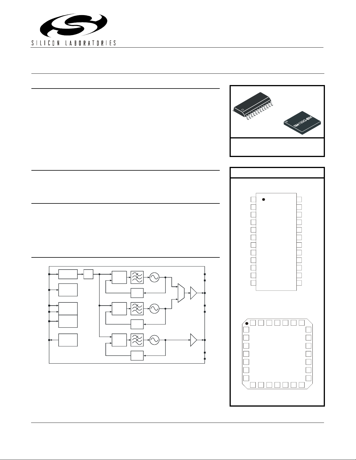
Description
The Si4133G is a monolithic integrated circuit that performs both IF and
dual-band RF synthesis for GSM and GPRS wireless communications
applications. Th e Si4133G includes th ree VCOs, loop fi lters, reference and
VCO dividers, and phase detectors. Divider and power down settings are
programmable through a three-wi re serial interface.
Functional Block Diagram
XIN
PWDNB
SDATA
SCLK
SENB
AUXOUT
Reference
Amplif ier
Power
Down
Control
Serial
Interfa c e
22-bit
Data
Register
Test
Mux
÷
65
Phase
Detector
Phase
Detector
Phase
Detector
÷
÷N
÷N
RF1
N
RF2
IF
RFLA
RFLB
RFOUT
RFLC
RFLD
IFOUT
IFLA
IFLB
VCO
S
Si4133G-BT
Ordering Information:
See page 28.
Pin Assignments
Si4133G-BT
SCLK
1
SDATA
2
GNDR
3
RFLD
4
RFLC
5
GNDR
6
RFLB
7
RFLA
8
GNDR
9
GNDR
10
RFOUT
11
VDDR
12
Si4133G-BM
GNDR
SDATA
SCLK
1
GNDR
2
RFLD
3
RFLC
4
GNDR
5
RFLB
6
RFLA
7
GNDR
8 9 10 11 12 13 14
SENB
SENB
24
VDDI
23
IFOU T
22
GNDI
21
IFLB
20
IFLA
19
GNDD
18
VDDD
17
GNDD
16
XIN
15
PWDNB
14
AUXOUT
13
VDDI
IFOU T
GNDI
22232425262728
21
GNDI
20
IFLB
19
IFLA
18
GNDD
17
VDDD
16
GNDD
15
XIN
GNDR
VDDR
GNDR
RFOUT
GNDD
PWDNB
AUXOUT
Patents pending
Rev. 1.1 4/01 Copyright © 2001 by Silicon Laboratories Si4133G-DS11
Page 2

Si4133G
2 Rev. 1.1
Page 3

Si4133G
T
ABLE OF
C
ONTENTS
Section Page
Electrical Specifications . . . . . . . . . . . . . . . . . . . . . . . . . . . . . . . . . . . . . . . . . . . . . . . . . 4
Functional Description . . . . . . . . . . . . . . . . . . . . . . . . . . . . . . . . . . . . . . . . . . . . . . . . . . 15
Serial Interface . . . . . . . . . . . . . . . . . . . . . . . . . . . . . . . . . . . . . . . . . . . . . . . . . . . . . . 15
Setting the VCO Center Frequencies . . . . . . . . . . . . . . . . . . . . . . . . . . . . . . . . . . . . . 15
Self-Tuning Algorithm . . . . . . . . . . . . . . . . . . . . . . . . . . . . . . . . . . . . . . . . . . . . . . . . . 16
Output Frequencies . . . . . . . . . . . . . . . . . . . . . . . . . . . . . . . . . . . . . . . . . . . . . . . . . . 17
PLL Loop Dynamics . . . . . . . . . . . . . . . . . . . . . . . . . . . . . . . . . . . . . . . . . . . . . . . . . . 17
RF and IF Outputs (RFOUT and IFOUT) . . . . . . . . . . . . . . . . . . . . . . . . . . . . . . . . . . 17
Reference Frequency Amplifier . . . . . . . . . . . . . . . . . . . . . . . . . . . . . . . . . . . . . . . . . 18
Power Down Modes . . . . . . . . . . . . . . . . . . . . . . . . . . . . . . . . . . . . . . . . . . . . . . . . . . 18
Auxiliary Output (AUXOUT) . . . . . . . . . . . . . . . . . . . . . . . . . . . . . . . . . . . . . . . . . . . . 18
Control Registers . . . . . . . . . . . . . . . . . . . . . . . . . . . . . . . . . . . . . . . . . . . . . . . . . . . . . . . 20
Pin Descriptions: Si4133G-BT . . . . . . . . . . . . . . . . . . . . . . . . . . . . . . . . . . . . . . . . . . . . . 24
Pin Descriptions: Si4133G-BM . . . . . . . . . . . . . . . . . . . . . . . . . . . . . . . . . . . . . . . . . . . . 26
Ordering Guide . . . . . . . . . . . . . . . . . . . . . . . . . . . . . . . . . . . . . . . . . . . . . . . . . . . . . . . . . 28
Si4133G Derivative Devices . . . . . . . . . . . . . . . . . . . . . . . . . . . . . . . . . . . . . . . . . . . . . . 28
Package Outline: Si4133G-BT . . . . . . . . . . . . . . . . . . . . . . . . . . . . . . . . . . . . . . . . . . . . . 29
Package Outline: Si4133G-BM . . . . . . . . . . . . . . . . . . . . . . . . . . . . . . . . . . . . . . . . . . . . 30
Contact Information . . . . . . . . . . . . . . . . . . . . . . . . . . . . . . . . . . . . . . . . . . . . . . . . . . . . . 32
Rev. 1.1 3
Page 4
Si4133G
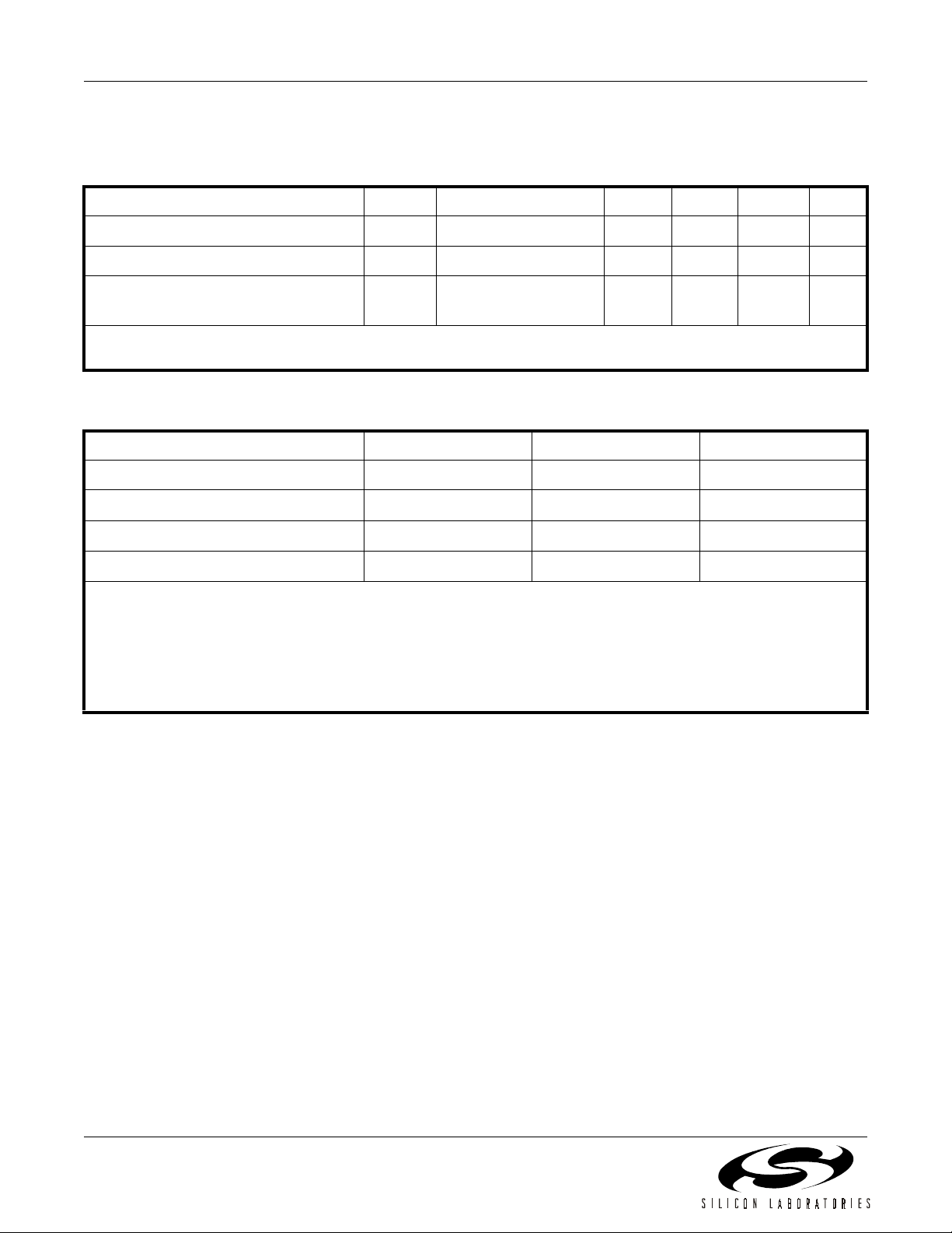
Electrical Specifications
Table 1. Recommended Operating Conditions
Parameter Symbol Test Condition Min Typ Max Unit
Ambient Temperature T
Supply Voltage V
Supply Voltages Difference V
Note: All minimum and maximum specifications are guaranteed and apply across the recommended operating conditions.
Typical values apply at 3.0 V and an operating temperature of 25°C unless otherwise stated.
Table 2. Absolute Maximum Ratings
1,2
DD
A
(V
(V
DDR
DDI
– V
– V
∆
DDD
DDD
),
)
–20 25 85 °C
2.7 3.0 3.6 V
–0.3 — 0.3 V
Parameter Symbol Value Unit
DC Supply Voltage V
Input Current
Input Voltage
3
3
Storage Temperature Range T
Notes:
1. Permanent device damage may occur if the above Absolute Maximum Ratings are exceeded. Functional operation
should be restricted to the conditions as specified in the operational sections of this data sheet. Exposure to absolute
maximum rating conditions for extended periods may affect device reliability.
2. This device is a high performan ce RF integrated circ uit with an ESD rating of < 2 kV. Handling and assembly of
this device should only be done at ESD-protected workstations.
3. For signals SCLK, SDATA, SENB, PWDNB and XIN.
I
V
DD
IN
IN
STG
–0.5 to 4.0 V
±10 mA
–0.3 to VDD+0.3 V
–55 to 150
o
C
4 Rev. 1.1
Page 5
Si4133G
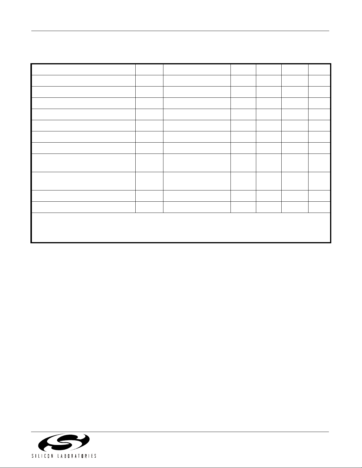
Table 3. DC Characteristics
(VDD = 2.7 to 3.6 V, TA = –20 to 85°C
Parameter Symbol Test Condition Min Typ Max Unit
Typical Supply Current
RF1 Mode Supply Current
RF2 Mode Supply Current
IF Mode Supply Current
1
1
1
1
Standby Current PWDNB = 0 — 1 — µA
High Level Input Voltage
Low Level Input Voltage
High Level Input Current
Low Level Input Current
High Level Output Voltage
Low Level Output Voltage
Notes:
1. RF1 = 1.55 GHz, RF2 = 1.2 GHz, IF = 800 MHz
2. For signals SCLK, SDATA, SENB, and PWDNB.
3. For signal AUXOUT.
2
2
2
2
3
3
V
IH
V
IL
I
IH
I
IL
V
OH
V
OL
RF1 and IF Operating — 18 31 mA
—1317mA
—1217mA
—1014mA
0.7 V
DD
——V
——0.3 VDDV
=
V
V
V
V
IH
= 3.6 V
DD
=
IL
=
DD
3.6 V,
0V,
3.6 V
–10 — 10 µA
–10 — 10 µA
IOH = –500 µA VDD–0.4 — — V
IOH = 500 µA — — 0.4 V
Rev. 1.1 5
Page 6
Si4133G
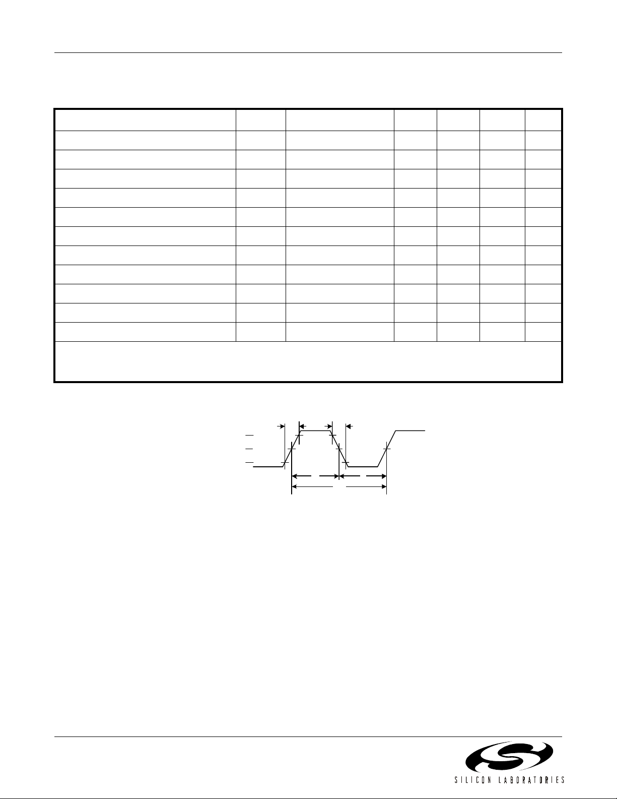
Table 4. Serial Interface Timing
(VDD = 2.7 to 3.6 V, TA = –20 to 85°C)
Parameter
1
SCLK Cycle Time t
SCLK Rise Time t
SCLK Fall Time t
SCLK High Time t
SCLK Low Time t
SDATA Setup Time to SCLK↑
SDATA Hold Time from SCLK↑
SENB↓ to SCLK↑ Delay Time
SCLK↑ to SENB↑ Delay Time
SENB↑ to SCLK↑ Delay Time
2
2
2
2
2
SENB Pulse Width t
Symbol Test Condition Min Typ Max Unit
Figure 1 40 — — ns
Figure 1 — — 50 ns
Figure 1 — — 50 ns
Figure 1 10 — — ns
Figure 1 10 — — ns
Figure 2 5 — — ns
Figure 2 0 — — ns
Figure 2 10 — — ns
Figure 2 12 — — ns
Figure 2 12 — — ns
Figure 2 10 — — ns
t
t
t
t
clk
t
su
hold
en1
en2
en3
w
r
f
h
l
Notes:
1. All timing is referenced to the 50% level of the waveform, unless otherwise noted.
2. Timing is not referenced to 50% level of waveform. See Figure 2.
SCLK
80%
50%
20%
t
r
t
f
t
h
t
l
t
clk
Figure 1. SCLK Timing Diagram
6 Rev. 1.1
Page 7
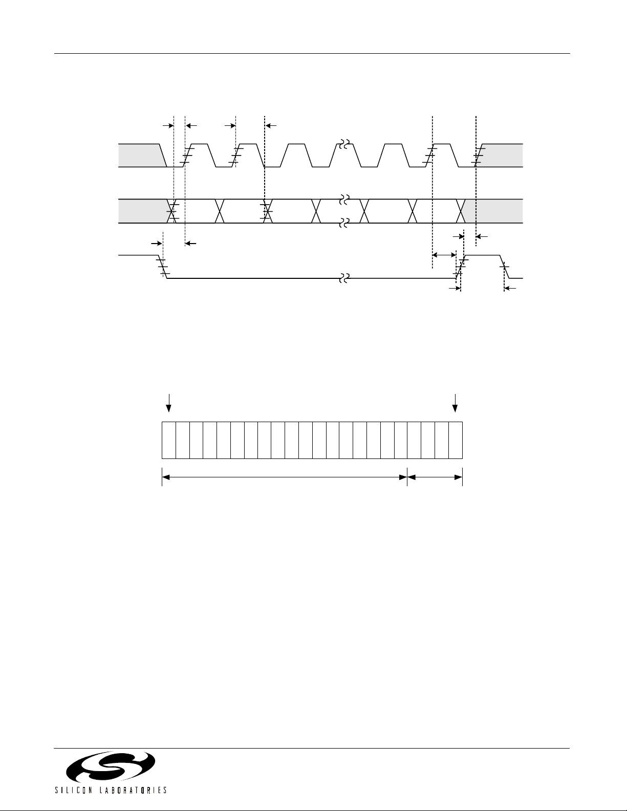
Si4133G
SCLK
SDATA
SENB
t
su
First bit
cloc ked in
t
hold
D17 D16 D15 A1 A0
t
en1
Figure 2. Serial Interface Timing Diagram
cloc ked in
t
en2
Last bit
t
en3
t
w
D17D16D15D14D13D12D11D10D9D8D7D6D5D4D3D2D1D0A3A2A1A
data
field
address
field
Figure 3. Serial Word Format
0
Rev. 1.1 7
Page 8
Si4133G
Table 5. RF and IF Synthesizer Characteristics
(VDD = 2.7 to 3.6 V, TA = –20 to 85°C)
Parameter
1
XIN Input Frequency f
Reference Amplifier Sensit ivity V
Symbol Test Condition Min Typ Max Unit
REF
REF
—13—MHz
0.5 — V
DD
V
PP
+0.3
Phase Detector Update Frequency f
RF1 Center Frequency Range
f
RF2 Center Frequency Range f
IF VCO Center Frequency f
Tuning Range from f
CEN
φ
CEN
CEN
CEN
f
φ
Note: L
= f
/R 200 KHz
REF
947 — 1720 MHz
789 — 1429 MHz
526 — 952 MHz
±10% –5 — 5 %
EXT
RF1 VCO Pushing Open loop — 0.5 — MHz/V
RF2 VCO Pushing — 0.4 — MHz/V
IF VCO Pushing — 0.3 — MHz/V
RF1 VCO Pulling VSWR = 2:1, all
RF2 VCO Pulling — 0.1 — MHz
phases, open loop
IF VCO Pulling — 0.1 — MHz
—0.4—MHz
PP
PP
PP
RF1 Phase Noise 1 MHz offset — –132 — dBc/Hz
3 MHz offset — –142 — dBc/Hz
RF1 Integrated Phase Error 100 Hz to 100 kHz — 0.9 — deg rms
RF2 Phase Noise 1 MHz offset — –134 — dBc/Hz
3 MHz offset — –144 — dBc/Hz
RF2 Integrated Phase Error 100 Hz to 100 kHz — 0.7 — deg rms
IF Phase Noise 100 kHz offset — –117 — dBc/Hz
IF Integrated Phase Error 100 Hz to 100 kHz — 0.4 — deg rms
RF1 Harmonic Suppression Second Harmonic — –26 — dBc
RF2 Harmonic Suppressio n — –26 — dBc
IF Harmonic Suppression — –26 — dBc
RFOUT Power Level
IFOUT Power Level
ZL = 50 Ω
ZL = 50 Ω
–7 –2 1 dBm
–8 –6 –1 dBm
RF1 Reference Spurs Offset = 200 kHz — –70 — dBc
Offset = 400 kHz — –75 — dBc
Offset = 600 kHz — –80 — dBc
R
F2 Reference Spurs Offset = 200 kHz — –75 — dBc
Offset = 400 kHz — –80 — dBc
Offset = 600 kHz — –80 — dBc
Power Up Request to Synthesizer
Ready Time, RF1, RF2, IF
2
Power Down Request to Synthesizer Off
3
Time
Notes:
1. RF1 = 1.55 GHz, RF2 = 1.2 GHz, IF = 550MHz for all parameters unless otherwise noted.
2. From power up request (PWDNB↑ or SENB↑ during a write of 1 to bits PDIB and PDRB in Register 2) to RF and IF
synthesizers ready (settled to within 0.1 ppm frequency error). Typical settling time to 5 degrees phase error is 120 µs.
3. From power down request (PWDNB↓, or SENB↑ during a write of 0 to bits PDIB and PDRB in Register 2) to supply
current equal to I
PWDN
.
t
t
pup
pdn
Figures 4, 5 — 140 — µs
Figures 4, 5 — — 100 ns
8 Rev. 1.1
Page 9
Si4133G
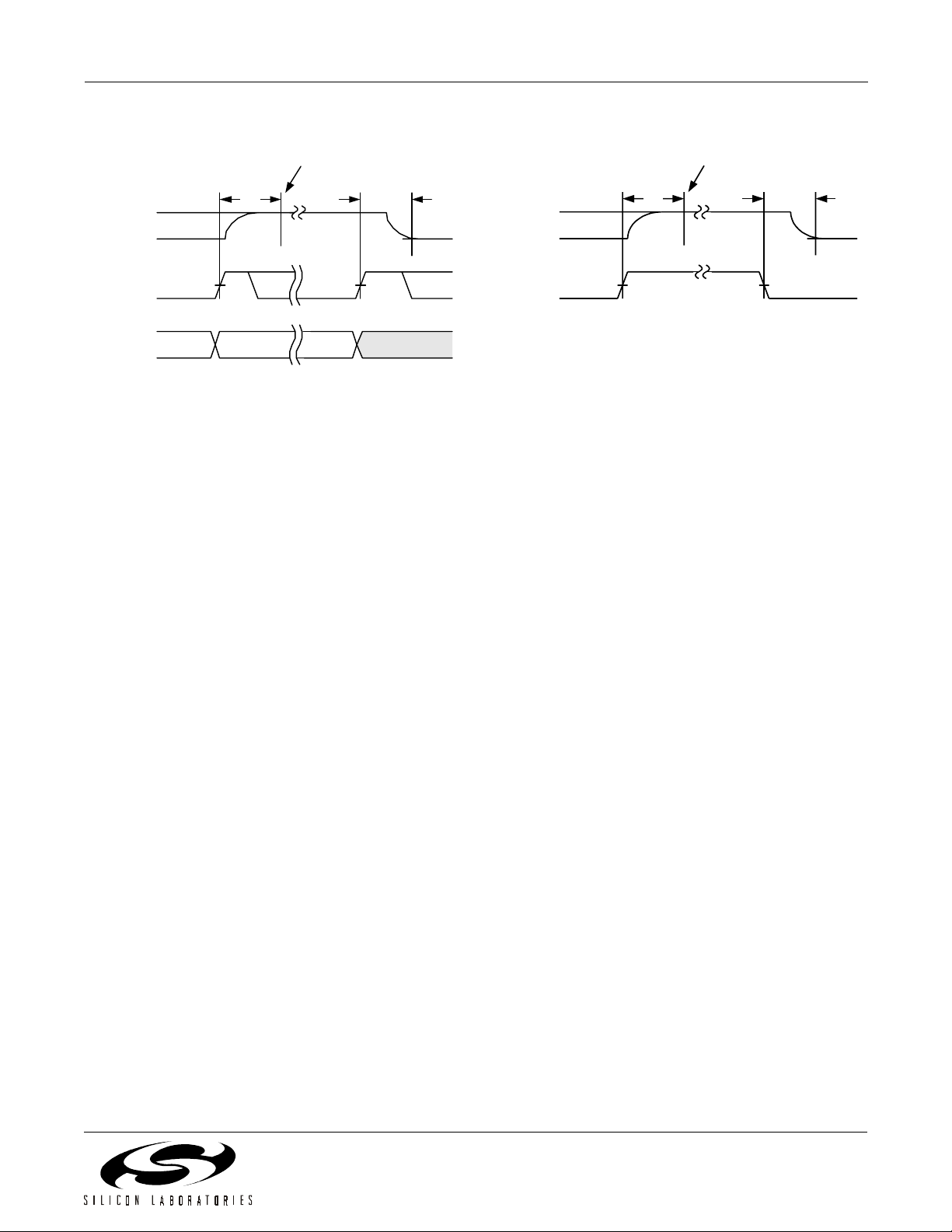
RF and IF syn thesize r s se t tled to
w i t hi n 0.1 ppm frequency error.
I
PWDN
t
I
T
pup
t
pdn
SENB
SDATA
PDIB = 1
PDRB = 1
PDIB = 0
PDRB = 0
Figure 4. Software Power Management Timing
Diagram
RF and IF synthesizers settled to
within 0.1 p pm frequency error.
I
PWD N
t
I
T
pup
t
pdn
PWDNB
Figure 5. Hardware Power Management Timing
Diagram
Rev. 1.1 9
Page 10
Si4133G
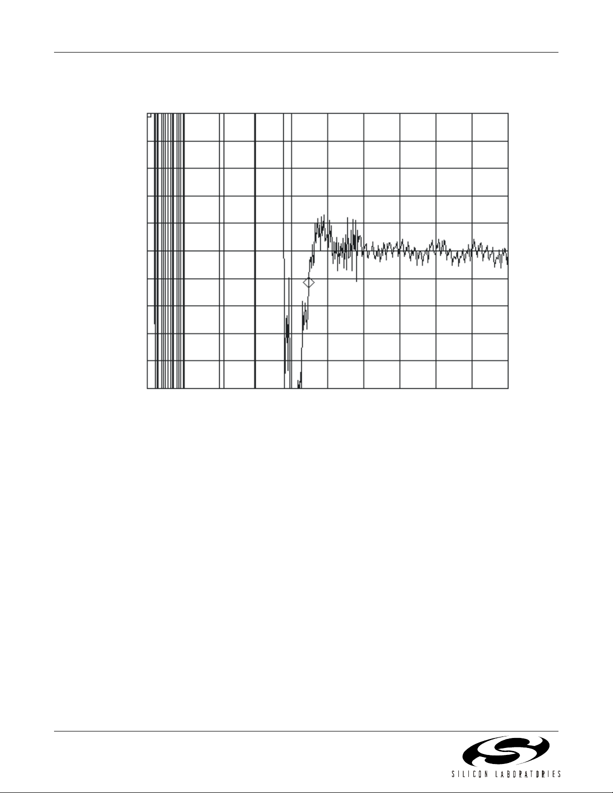
TRACE A: Ch1 FM Gate Time
800
Real
160
/div
Axis is 0.1 ppm/div
Hz
Hz
A Offset
133.59375 us
-800
Hz
Start: 0 s
Figure 6. Typical Transient Response RF1 at 1.6 GHz
with 200 kHz Phase Detector Update Frequency
Stop: 299.21875 us
10 Rev. 1.1
Page 11

−60
−70
−80
−90
−100
−110
Phase Noise (dBc/Hz)
−120
−130
Si4133G
−140
2
10
3
10
Offset Frequency (Hz)
4
10
Figure 7. Typical RF1 Phase Noise at 1.6 GHz
with 200 kHz Phase Detector Update Frequency
5
10
6
10
Figure 8. Typical RF1 Spurious Response at 1.6 GHz
with 200 kHz Phase Detector Update Frequency
Rev. 1.1 11
Page 12

Si4133G
−60
−70
−80
−90
−100
−110
Phase Noise (dBc/Hz)
−120
−130
−140
2
10
3
10
Offset Frequency (Hz)
4
10
Figure 9. Typical RF2 Phase Noise at 1.2 GHz
with 200 kHz Phase Detector Update Frequency
5
10
6
10
Figure 10. Typical RF2 Spurious Response at 1.2 GHz
with 200 kHz Phase Detector Update Frequency
12 Rev. 1.1
Page 13

−70
−80
−90
−100
−110
−120
Phase Noise (dBc/Hz)
−130
−140
Si4133G
−150
2
10
3
10
Offset Frequency (Hz)
4
10
Figure 11. Typical IF Phase Noise at 550 MHz
with 200 kHz Phase Detector Update Frequency
5
10
6
10
Figure 12. IF Spurious Response at 550 MHz
with 200 kHz Phase Detector Update Frequency
Rev. 1.1 13
Page 14

Si4133G
Printed Trace
Indu c to rs
RFOUT
From
System
Controller
From
System
Controller
560pF 2nH
Si4133G-BT
0.022µF
1
SCLK
2
SDATA
3
GNDR
4
RFLD
5
RFLC
6
GNDR
7
RFLB
8
RFLA
9
GNDR
10
GNDR
11
V
RFOUT
DD
12
VDDR
PWDNB
AUXOUT
SENB
VDDI
IFO U T
GNDI
IFLB
IFLA
GNDD
VDDD
GNDD
XIN
24
µ
0.022
0.022µ
F
F
V
DD
23
22
21
20
19
18
V
DD
17
16
15
14
13
Figure 13. Typical Application Circuit: Si4133G-BT
V
DD
0.022
µ
F
560pF10nH
Printed Trace
Inductor or
Ch ip In d u c to r
560pF
10nH
IFO U T
560 pF
External Clock
PDWNB
AUXOUT
IFO UT
Printed Trace
Ind u c to r s
PWDNB
22232425262728
1
2
3
4
5
6
7
GNDR
GNDR
RFLD
RFLC
GNDR
RFLB
RFLA
GNDR
GNDR
GNDR
GNDR
8 9 10 11 12 13 14
V
DD
0.022
µ
SCLK
SDATA
Si4133G-BM
GNDR
RFOUT
GNDR
RFOUT
GNDR
RFOUT
F
SENB
VDDR
VDDR
VDDR
VDDI
AUXOUT
AUXOUT
AUXOUT
IFOUT
PWDNB
PWDNB
PWDNB
GNDI
GNDD
VDDD
GNDD
GNDD
GNDD
GNDD
GNDI
IFL B
IFL A
XIN
21
20
19
18
17
16
15
V
DD
Figure 14. Typical Application Circuit: Si4133G-BM
Printed Trace
Ind u c to r o r
Ch ip Inducto r
0.022
µ
F
560pF
560pF
2nH
External Clock
AUXOUT
RFOUT
14 Rev. 1.1
Page 15

Si4133G
1
Functional Description
The Si4133G is a monolithic integrated circuit that
performs IF and dual-band RF synthesis for many
wireless applications such as GSM, DCS1800, and
PCS1900. Its fast transient response also makes the
Si4133G especially well suited to GPRS and HSCSD
multislot applications where channel switching and
settling times are critical. This integrated circuit (IC),
with a minimum number of external components, is all
that is necessary to imple ment the frequency synthesis
function.
The Si4133G has three complete phase-locked loops
(PLLs) with integrated voltage-controlled oscillators
(VCOs). The low ph ase noise of the VCOs mak es the
Si4133G suitable for use in demanding wireless
communications applications. Also integrated are phase
detectors, loop filter s, and reference divi ders. The IC is
programmed through a three-wire serial interface.
One PLL is provided for IF synthes is, a nd two PL Ls are
provided for dual-band RF synthesis. One RF VCO is
optimized to have its center frequency set between
947 MHz and 1720 MHz, whil e the second RF VCO is
optimized to have its center frequency set between
789 MHz and 1429 MHz. The IF VCO is optimized to
have its center frequency set between 526 MHz and
952 MHz . Each PLL can adjust its outp ut frequency by
±5% relative to its VCO center frequency.
The center frequency of each of the thr ee VCOs is set
by connection of an external inductance. Inaccuracies in
the value of the inductance are comp ensated for by th e
Si4133G’s proprietary self-tuning algorithm. This
algorithm is initia ted each time the PLL is powered-up
(by either the PW DNB pin or by software) and /or each
time a new output frequency is programmed.
The two RF PLLs share a common output pin, so only
one PLL is active at a given time. Because the two
VCOs can be set to have widely separated center
frequencies, the RF output can be programmed to
service different frequency bands, thus making the
Si4133G ideal for use in dual-band cellular handsets.
The unique PLL architecture used in the Si4133G
produces a transient r esponse that is supe rior in speed
to fractional-N architectures without suffering the high
phase noise or spurious modulation effects often
associated with those designs.
The Si4133G is prog rammed serially with 22-bit wor ds
comprised of 18-bit da ta fields and 4-bit addr ess fields.
When the serial interface is enabled (i.e., when SENB is
low) data and address bits on the SDATA pin are
clocked into an internal s hift register on the risin g edge
of SCLK. Data in the shift re gis ter i s t hen trans fer red o n
the rising edge of SENB into the internal data register
addressed in the address field. The serial interface is
disabled when SENB is high.
Table 10 on page 20 summarizes the data register
functions and addr esses. The internal s hift register will
ignore any leading bits before the 22 required bits.
Setting the VCO Center Frequencies
The PLLs can adju st the IF and RF outp ut frequencies
±5% with respect to their VCO center frequencies. Each
center frequency is established by the value of an
external inductance connected to the respective VCO.
Manufacturing tolerances of ±10% for the external
inductances are acceptable. The Si4133G will
compensate for inaccuracies in each inductance by
executing a self-tu ning algorithm following PLL powerup or following a change in the programmed output
frequency.
Because the total tank inductance is in the low nH
range, the inductance of the package needs to be
considered in determining the correct external
inductance. The total inductance (L
each VCO is the su m of the externa l inductanc e (L
and the package i nductance (L
nominal capacitance (C
NOM
PKG
) in parallel with the total
inductance, and the center frequency is as follows:
f
CEN
---------------------------------------------=
2π L
⋅
TOTCNOM
or
f
CEN
----------------------------------------------------------------------=
2π L
1
+()C
PKGLEXT
Tables 6 and 7 summarize these characteristics for
each VCO.
) presented to
TOT
EXT
). Each VCO has a
⋅
NOM
)
Serial Interface
A timing diagram for the serial interface is shown in
Figure 2 on page 7. Figure 3 on page 7 shows the
format of the serial word.
Rev. 1.1 15
Page 16

Si4133G
Table 6. Si4133G-BT VCO Characteristics
VCO Fcen Range
(MHz)
Min Max Min Max
RF1 947 1720 4.3 2.0 0.0 4.6
RF2 789 1429 4.8 2.3 0.3 6.2
IF 526 952 6.5 2.1 2.2 12.0
Cnom
(pF)
Lpkg
(nH)
Lext Range
(nH)
Table 7. Si4133G-BM VCO Characteristics
VCO Fcen Range
(MHz)
Min Max Min Max
RF1 947 1720 4.3 1.5 0.5 5.1
RF2 789 1429 4.8 1.5 1.1 7.0
IF 526 952 6.5 1.6 2.7 12.5
Cnom
(pF)
L
PKG
2
L
PKG
2
Lpkg
(nH)
Lext Range
(nH)
L
EXT
Figure 15. External Inductance Connection
As a design example, suppose it is desired to
synthesize frequencies in a 25 MHz band between
1120 MHz and 1145 MHz. The center frequenc y should
be defined as midway between the two extremes, or
1132.5 MHz. The PLL will be able to adjust the VCO
output frequency ±5% of the center frequency, or
±56.6 MHz of 1132.5 MHz (i.e., from approximately
1076 MHz to 1189 MHz, more than enough for this
example). The RF2 VCO has a C
4.1 nH in ductance (corre ct to two digits) in paral lel with
this capacitance w ill yield the desired c enter frequen cy.
An external inductan ce of 1.8 nH sh ould be connected
between RFLC and RFLD a s shown in Figure 15. Th is,
of 4.8 pF, and a
NOM
in addition to 2.3 nH of L
(Si4133G-BT), wi ll pr e sent
PKG
the correct total inductance to the VCO. In
manufacturing, the extern al inductance can vary ±10%
of its nominal value an d the Si413 3G wi ll correc t for th e
variation with the self-tuning algorithm.
In most cases, particularly for the RF VCOs, the
requisite value of the external inductance is small
enough to allow a PC boar d trace to be utilized . During
initial board layou t, a length of trace approxim ating the
desired inductanc e can be used . For more in formation,
please refer to Application Note 31.
Self-Tuning Algorithm
The self-tuning algorithm is initiated immediately
following power-up of a PLL or, if the PLL is already
powered, following a c hange in its programmed o utput
frequency. This algorithm attempts t o tune the VCO so
that its free-running frequency is near the desired output
frequency. In so doing, the algorithm will compensate
for manufacturing tolerance errors in the value of the
external inductance conn ected to the VCO. It will also
reduce the frequency error for which the PLL must
correct to get the prec ise desi red ou tput fr equency. The
self-tuning algorith m will leave the VCO oscillating at a
frequency in error by somewhat less than 1% of the
desired output frequency.
After self-tuning, the PLL controls the VCO oscillation
frequency. The PLL will complete frequency locking,
eliminatin g any remaining frequency error. Thereafter, it
will maintain frequency-lock, compensating for effects
caused by temperature and supply voltage variations.
The Si4133G’s self-tuning algorithm will compensate for
component value errors at any temperature within the
specified temperature r ange. Howeve r, the ability of the
PLL to compensate for drift in component values that
occur after self-tuning is limited. For external
inductances with temperature coefficients around
±150 ppm/
changes in temperature of approximately ±30
Applications where the PLL is regularly powere d down
(such as GSM) or switched between channels minimize
or eliminate the potential effects of temperature drift
because the VCO is r e-tuned when it is powered up or
when a new frequency is programmed. In applicati ons
where the ambient temperature can drift substantially
after self-tuning, it may be necessary to monitor the
LDETB (lock-detect bar) s ignal on the AUXOUT pin to
determine the locking st ate of the PLL. (See "Auxiliary
Output (AUXOUT)" on page 18 for how to select
LDETB.)
The LDETB signal is normally low after self-tuning is
completed but will rise to a logic high condition when
o
C, the PLL will be able to maintain lock for
o
C.
16 Rev. 1.1
Page 17

Si4133G
either the IF or RF PLL nears the limit of its
compensation range (LDETB will also be high when
either PLL is executin g the self-tuning algorithm). The
output frequency wi ll still be locked when LDETB goes
high, but the PLL will eventually lose lock if the
temperature continues to drift in the same direction.
Therefore, if LDETB goes high both the IF and RF PLLs
should promptly be re-tu ned by initiating th e self-tuning
algorithm.
Output Frequencies
The IF and RF output frequencies are set by
programming the N-Div ider regis ters. E ach RF P LL has
its own N register and can be programmed
independently. All three PLL R dividers are fixed at
R = 65 to yield a 200 kHz phase detector update rate
from a 13 MHz reference freq uency. Programmin g the
N-Divider register for either RF1 or RF2 automatically
selects the associated output.
The reference frequ ency on the XIN pin is divided b y R
and this signal is the inpu t to the PLL’s phase detector.
The other input to the phase detecto r is the PLL’s VCO
output frequency divided by N. The PLL works to mak e
these frequencies equal. That is, after an initial transient
f
------------
OUT
N
f
REF
-----------=
65
or
OUT
------
65
⋅=
f
REF
f
N
For XIN = 13 MHz this simplifies to
f
OUT
N 200 kHz⋅=
The integer N is set b y program ming th e RF1 N-Divider
register (Register 3), the RF2 N-Divider register
(Register 4), and the IF N-Divider register (Register 5).
Each N divider is im plemented as a conventional hig h
speed divider. That is, it consists of a dual-modulus
prescaler, a swallow counter, and a lower speed
synchronous counter. However, the calculation of thes e
values is done automatically. Only the appropriate N
value needs to be programmed.
PLL Loop Dynamics
The transient response for each PLL has been
optimized for a GSM application. VCO gain, phase
detector gain, and loop filter characteristics are not
programmable.
The settling time for eac h PLL is direc tly proportio nal to
its phase detector update period Tφ (Tφ equals 1/fφ). For
a GSM application with a 13 MHz reference freq uency,
the RF and IF PLLs Tφ =5µS. During the first 6.5
update periods, the Si4133G executes the self-tuning
algorithm. Thereafter the PLL controls the output
frequency. Because of the unique architecture of the
Si4133G PLLs, the time required to settle the output
frequency to 0.1 ppm error is approximately 21 update
periods. Thus, the total time af ter power -up or a ch ang e
in programmed frequency until the synthesized
frequency is well sett led (including time for self -tuning)
is around 28 update periods or 140 µS.
RF and IF Outputs (RFOUT and IFOUT)
The RFOUT pin is driven by an amplifier that buffers the
output pin from the RF VC Os, and must be coupled to
its load through an A C coupl ing ca pacito r. The amplifier
receives its input from either the RF1 or RF2 VCO,
depending upon which N-Divider register was last
written. For example, programming the N-Divider
register for RF1 automatically selects the RF1 VCO
output.
A matching network is required to maximize power
delivered into a 50 Ω load. Th e network consis ts of a 2
nH series inductan ce, which m ay be re alized with a PC
board trace, connected between the RFOUT pin and
the AC coupling capacitor. The network is made to
provide an adequate matc h for both the RF1 and RF2
frequency bands, and also filters the output signal to
reduce harmonic dis tortion. A 50 Ω load is not required
for proper operation of the Si4133G. Depending on
transceiver requirements, the matching network may
not be needed. See Figure 16.
560 pF
RFOUT
2 nH
50
Ω
Figure 16. RFOUT 50 Ω
The IFOUT pin is driv en by an a mplifier tha t buffers the
output pin from the IF VCO. The IFOUT pin must be
coupled to its l oad thr ough an AC cou pling capa citor. A
matching network is required to maximize power
delivered into a 50 Ω load. See Figure 17.
Ω Test Circuit
Ω Ω
Rev. 1.1 17
Page 18

Si4133G
)
560 pF
IFO U T
L
MATCH
50
Ω
Figure 17. IFOUT 50 Ω
Table 8. L
Frequency L
500–600 MHz 40 nH
600–800 MHz 27 nH
800–1 GHz 18 nH
The IF output level is dependent upon the load.
Figure 18 displays the output level versus load
resistance for a variety of output frequencies.
450
400
350
LPWR=0
300
250
200
Output Voltage (mVrms
150
100
50
0
0 200 400 600 800 1000 1200
Ω Test Circuit
Ω Ω
LPWR=1
Values
ΩΩΩΩ
)
MATCH
Load Resistance (
MATCH
Reference Frequency Amplifier
The Si4133G provides a referenc e frequency amplifier.
If the driving signal has CMOS levels it can be
connected directly to the XIN pin. Otherwise, the
reference frequency signal should be AC coupl ed to th e
XIN pin through a 560 pF capacitor.
Power Down Modes
Table 9 summariz es the power down functionality. The
Si4133G can be powe red down by taking the PWDNB
pin low or by setting bits in the Power Down register
(Register 1). When the PWDNB pin is lo w, the Si4133G
will be powered down regardless of the Power Down
register settings. When the PWDNB pin is high, power
management is under control of the Power Down
register bits.
The reference frequen cy amplifier, IF, and RF sections
of the Si4133G circuitry can be individually powered
down by setting the Pow er Down r egister bits PDIB and
PDRB low, respectively. The reference frequency
amplifier will also be powered up if either of the PDRB
or PDIB bits are hi gh. Al so, se tting th e AUTOPDB b it to
1 in the Main Configuration register (Register 0) is
equivalent to setting both bits in the Power Down
register to 1. T he ser ial inter face r emains availab le and
can be written in all power down modes.
Auxiliary Output (AUXOUT)
The signal appearing on AUXOUT is selected by setting
the AUXSEL bits in the Main Configuration register
(Register 0).
The LDETB signal can be selected by setting the
AUXSEL bits to 11. As discussed previously, this signal
can be used to indicate that the IF or RF PLL is about to
lose lock due to excessive ambient temperature drift and
should be re-tuned.
Figure 18. Typical IF Output Voltage vs. Load
Resistance at 550 MHz
For resistive lo ads greater than 500 Ω the output level
saturates and the bias currents in the IF output amplifier
are higher than they need be. The LPWR bit in the Main
Configuration register (Register 0) can be set to 1 to
reduce the bias currents and therefore reduce the
power dissipated by the IF amplifier. For loads less than
500 Ω LPWR should be set to 0 to maximize the output
level.
18 Rev. 1.1
Page 19

Table 9. Power Down Configuration
PWDNB Pin AUTOPDB PDIB PDRB IF Circuitry RF Circuitry
Si4133G
PWDNB = 0
PWDNB = 1
xxxOFFOFF
000OFFOFF
001OFFON
010ONOFF
011ONON
1xxONON
Rev. 1.1 19
Page 20

Si4133G
Control Registers
T able 10. Register Summary
Register Name Bit 17Bit 16Bit 15Bit 14Bit 13Bit 12Bit 11Bit 10Bit 9Bit 8Bit 7Bit6Bit5Bit4Bit3Bit 2Bit1Bit
0
0Main
Configuration
0000
AUXSEL
[1:0]
000000
LPWR
AUTO
0
PDB
010
1 Reserved
2 Power Down0000000000000000
3RF1 N Divider N
4RF2 N Divider0 N
5IF N Divider00 N
RF1
[17:0]
[16:0]
RF
IF
[15:0]
PDIB PDRB
6 Reserved
.
.
.
15 Reserved
Note: Registers 1 and 6–15 are reserv ed. W rites to thes e registe rs ma y result in unpredic table behavio r. Any register not listed
here is rese rved and sho uld not be written.
20 Rev. 1.1
Page 21

Si4133G
Register 0. Main Configuration Address Field = A[3:0] = 0000
Bit D17 D16 D15 D14 D13 D12 D11 D10 D9 D8 D7 D6 D5 D4 D3 D2 D1 D0
Name 0000AUXSEL
0 00000
LPWR
0
[1:0]
Bit Name Function
17:14 Reserved Program to zero.
13:12 AUXSEL
[1:0]
Auxiliary Output Pin Definition.
00 = Reserved.
01 = Force output low.
10 = Reserved.
11 = Lock Detect—LDETB.
11:6 Reserved Program to zero.
5LPWROutput Power-Level Settings for IF Synthesizer Circuit.
0 = R
1 = R
< 500 Ω—normal power mode.
LOAD
≥ 500 Ω—low power mode.
LOAD
4 Reserved Program to zero.
3 AUTOPDB Auto Power Down
0 = Software powerdown is controlled by Register 2.
1 = Equivalent to setting al l bits in Register 2 = 1.
2 Reserved Program to zero.
AUTO
PDB
010
1 Reserved Program to one.
0 Reserved Program to zero.
Rev. 1.1 21
Page 22

Si4133G
Register 2. Power Down Address Field (A[3:0]) = 0010
Bit D17 D16 D15 D14 D13 D12 D11 D10 D9 D8 D7 D6 D5 D4 D3 D2 D1 D0
Name 000000000000000 0
PDIB PDRB
Bit Name Function
17:2 Reserved Program to zero.
1PDIBPower Down IF Synthesizer.
0 = IF synthesizer powered down.
1 = IF synthesizer on.
Note: Always program to 0 for Si4113G.
0 PDRB Power Down RF Synthesizer.
0 = RF synthesizer powered down.
1 = RF synthesizer on.
Note: Always program to 0 for Si4112G.
Register 3. RF1 N Divider Address Field (A[3:0]) = 0011
Bit D17D16D15D14D13D12D11D10D9D8D7D6D5D4D3D2D1D0
Name N
RF1
[17:0]
Bit Name Function
17:0 N
[17:0] N Divider for RF1 Synthesizer.
RF1
Register reserved for Si4112G, Si4122G. Writes to this register may result in unpredictable behavior.
22 Rev. 1.1
Page 23

Si4133G
Register 4. RF2 N Divider Address Field = A[3:0] = 0100
Bit D17D16D15D14D13D12D11D10D9D8D7D6D5D4D3D2D1D0
Name 0N
RF2
[16:0]
Bit Name Function
17 Reserved Program to zero.
16:0 N
[16:0] N Divider for RF2 Synthesizer.
RF2
Register reserved for Si4112G, Si4123G. Writes to this register may result in
unpredictable behavior.
Register 5. IF N Divider Address Field (A[3:0]) = 0101
Bit D17D16D15D14D13D12D11D10D9D8D7D6D5D4D3D2D1D0
Name 00 N
[15:0]
IF
Bit Name Function
17:16 Reserved Program to zero.
15:0 N
[15:0] N Divider for IF Synthesizer.
IF
Register reserved for Si4113G. Writes to this register may result in
unpredictable behavi or.
Rev. 1.1 23
Page 24

Si4133G
Pin Descriptions: Si4133G-BT
SCLK
SDATA
GNDR
RFLD
RFLC
GNDR
RFLB
RFLA
GNDR
GNDR
RFOUT
VDDR
1
2
3
4
5
6
7
8
9
10
11
12
24
23
22
21
20
19
18
17
16
15
14
13
SENB
VDDI
IFO U T
GNDI
IFLB
IFLA
GNDD
VDDD
GNDD
XIN
PWDNB
AUXOUT
Pin Number(s) Name Description
1 SCLK Serial clock input
2 SDATA Serial data input
3, 6, 9, 10 GNDR Common ground for RF analog circuitry
4, 5 RFLC, RFLD Pins for inductor connection to RF2 VCO
7, 8 RFLA, RFLB Pins for inductor connection to RF1 VCO
11 RFOUT Radio frequency (RF) output of the selected RF VCO
12 VDDR Supply voltage for the RF analog circuitry
13 AUXOUT Auxiliary output
14 PWDNB Power down input pin
15 XIN Reference frequency amplifier input
16, 18 GNDD Common ground for digital circuitry
17 VDDD Supply voltage for digital circuitry
19, 20 IFLA, IFLB Pins for inductor connection to IF VCO
21 GNDI Common ground for IF analog circuitry
22 IFOUT Intermediate frequency (IF) output of the IF VCO
23 VDDI Supply voltage for IF analog circuitry
24 SENB Enable serial port input
24 Rev. 1.1
Page 25

Si4133G
Table 11. Pin Descriptions for Si4133G Derivatives—TSSOP
Pin Number Si4133G-BT Si4123G-BT Si4122G-BT Si4113G-BT Si4112G-BT
1 SCLK SCLK SCLK SCLK SCLK
2 SDATA SDATA SDATA SDATA SDATA
3 GNDR GNDR GNDR GNDR GNDD
4 RFLD GNDR RFLD RFLD GNDD
5 RFLC GNDR RFLC RFLC GNDD
6 GNDR GNDR GNDR GNDR GNDD
7 RFLB RFLB GNDR RFLB GNDD
8 RFLA RFLA GNDR RFLA GNDD
9 GNDR GNDR GNDR GNDR GNDD
10 GNDR GNDR GNDR GNDR GNDD
11 RFOUT RFOUT RFOUT R FOUT GNDD
12 VDDR VDDR VDDR VDDR VDDD
13 AUXOUT AUXOUT AUXOUT AUXOU T AUXOUT
14 PWDNB PWDNB PWDNB PWDNB PWDNB
15 XIN XIN XIN XIN XIN
16 GNDD GNDD GNDD GNDD GNDD
17 VDDD VDDD VDDD VDDD VDDD
18 GNDD GNDD GNDD GNDD GNDD
19 IFLA IFLA IFLA GNDD IFLA
20 IFLB IFLB IFLB GNDD IFLB
21 GNDI GNDI GNDI GNDD GNDI
22 IFOUT IFOUT IFOUT GNDD IFOUT
23 VDDI VDDI VDDI VDDD VDDI
24 SENB SENB SENB SENB SENB
Rev. 1.1 25
Page 26

Si4133G
Pin Descriptions: Si4133G-BM
GNDR
SDATA
SCLK
SENB
VDDI
IFO UT
GNDI
22232425262728
GNDR
RFLD
RFLC
GNDR
RFLB
RFLA
GNDR
1
2
3
4
5
6
7
8 9 10 11 12 13 14
GNDR
GNDR
VDDR
RFOUT
AUXOUT
PWDNB
21
GNDI
20
IFLB
19
IFLA
18
GNDD
17
VDDD
16
GNDD
15
XIN
GNDD
Pin Number(s) Name Description
1, 4, 7–9, 28 GNDR Common ground for RF analog circuitry
2, 3 RFLC, RFLD Pins for inductor connection to RF2 VCO
5,6 RFLA, RFLB Pins for inductor connection to RF1 VCO
10 RFOUT Radio frequency (RF) output of the selected RF VCO
11 VDDR Supply voltage for the RF analog circuitry
12 AUXOUT Auxiliary output
13 PWDNB Power down input pin
14, 16, 18 GNDD Common ground for digital circuitry
15 XIN Reference frequency amplifier input
17 VDDD Supply voltage for digital circuitry
19, 20 IFLA, IFLB Pins for inductor connection to IF VCO
21, 22 GNDI Common ground for IF analog circuitry
23 IFOUT Intermediate frequency (IF) output of the IF VCO
24 VDDI Supply voltage for IF analog circuitry
25 SENB Enable serial port input
26 SCLK Seri al cl oc k inp ut
27 SDATA Serial data input
26 Rev. 1.1
Page 27

Si4133G
Table 12. Pin Descriptions for Si4133G Derivatives—MLP
Pin Number Si4133G-BM Si4123G-BM Si4122G-BM Si4113G-BM Si4112G-BM
1 GNDR GNDR GNDR GNDR GNDD
2 RFLD GNDR RFLD RFLD GNDD
3 RFLC GNDR RFLC RFLC GNDD
4 GNDR GNDR GNDR GNDR GNDD
5 RFLB RFLB GNDR RFLB GNDD
6 RFLA RFLA GNDR RFLA GNDD
7 GNDR GNDR GNDR GNDR GNDD
8 GNDR GNDR GNDR GNDR GNDD
9 GNDR GNDR GNDR GNDR GNDD
10 RFOUT RFOUT RFOUT RFOUT GNDD
11 VDDR VDDR VDDR VDDR VDDD
12 AUXOUT AUXOUT AUXOUT AUXOUT AUXOUT
13 PWDNB PWDNB PWDNB PWDNB PWDNB
14 GNDD GNDD GNDD GNDD GNDD
15 XIN XIN XIN XIN XIN
16 GNDD GNDD GNDD GNDD GNDD
17 VDDD VDDD VDDD VDDD VDDD
18 GNDD GNDD GNDD GNDD GNDD
19 IFLA IFLA IFLA GNDD IFLA
20 IFLB IFLB IFLB GNDD IFLB
21 GNDI GNDI GNDI GNDD GNDI
22 GNDI GNDI GNDI GNDD GNDI
23 IFOUT IFOUT IFOUT GNDD IFOUT
24 VDDI VDDI VDDI VDDD VDDI
25 SENB SENB SENB SENB SENB
26 SCLK SCLK SCLK SCLK SCLK
27 SDATA SDATA SDATA SDATA SDATA
28 GNDR GNDR GNDR GNDR GNDD
Rev. 1.1 27
Page 28

Si4133G
Ordering Guide
Ordering Part
Number
Si4133G-BT*
Description Operating
Temperature
RF1/RF2/IF –20 to 85
o
C
Si4133G-BM
Si4123G-BT*
RF1/IF –20 to 85
o
C
Si4123G-BM
o
Si4122G-BT*
RF2/IF –20 to 85
C
Si4122G-BM
o
Si4113G-BT*
RF1/RF2 –20 to 85
C
Si4113G-BM
o
Si4112G-BT*
IF –20 to 85
C
Si4112G-BM
*Note: TSSOP not recommended for new designs.
Si4133G Derivative Devices
The Si4133G performs both I F and dual-band RF frequency synth esis. The Si 4112G, Si4113G, Si4122G, and the
Si4123G are derivat ives of this device. Table 13 outlines whic h synthesizers each derivati ve device features as
well as which pins and registers coincide with each synthesizer.
Table 13. Si4133G Derivatives
Name Synthesizer Pins Registers
Si4112G IF IFLA, IFLB N
, RIF, PDIB, IFDIV , LPWR, AUTOPDB = 0,
IF
PDRB = 0
Si4113G RF1, RF2 RFLA, RFLB, RFLC, RFLD N
RF1
, N
RF2
, R
RF1
, R
, PDRB, AUTOPDB = 0,
RF2
PDIB = 0
Si4122G RF2, IF RFLC, RFLD, IFLA, IFLB N
Si4123G RF1, IF RFLA, RFLB, IFLA, IFLB N
Si4133G RF1, RF2, IF RFLA, RFLB, RFLC, RFLD,
IFLA, IFLB
N
RF2
RF1
RF1
, R
, PDRB, NIF, RIF, PDIB, LPWR
RF2
, R
, PDRB, NIF, RIF, PDIB, LPWR
RF1
, N
, R
RF1
, R
RF2
RF2
PDIB, LPWR
, PDRB, NIF, RIF,
28 Rev. 1.1
Page 29

Package Outline: Si4133G-BT
E1 E
R1
Si4133G
2
θ
S
R
θ1
e
D
A2
A
b
A1
L
L1
θ3
Figure 19. 24-pin Thin Small Shrink Outline Package (TSSOP)
Table 14. Package Diagram Dimensions
Symbol Millimeters
Min Nom Max
A — 1.10 1.20
A1 0.05 — 0 .15
A2 0.80 1.00 1.05
b0.19—0.30
c0.09—0.20
D 7.70 7.80 7.90
e0.65 BSC
E6.40 BSC
E1 4.30 4.40 4.50
L 0.45 0.60 0.75
L1 1.00 REF
R0.09 — —
R1 0.09 — —
S0.20— —
θ10 —8
θ2 12 REF
θ3 12 REF
c
Rev. 1.1 29
Page 30

Si4133G
Package Outline: Si4133G-BM
Figure 20. 28-Pin Micro Leadframe Package (MLP)
Table 15. Package Dimensions
Controlling Dimension: mm
Symbol Millimeters
Min Nom Max
A — 0.90 1.00
A1 0.00 0.01 0.05
b 0.18 0.23 0.30
D5.00 BSC
D1 4.75 BSC
E5.00 BSC
E1 4.75 BSC
N28
Nd 7
Ne 7
e0.50 BSC
L 0.50 0.60 0.75
θ
30 Rev. 1.1
12
°
Page 31

Si4133G
N
OTES
:
Rev. 1.1 31
Page 32

Si4133G
Contact Information
Silicon Laborato ries Inc.
4635 Boston Lane
Austin, Texas 78735
Tel:1+ (512) 416-8500
Fax:1+ (512) 416-9669
Toll Free:1+ (877) 444-3032
Email: productinfo@silabs.com
Internet: www.silabs.com
The information in this document is believed to be accurate in all respects at the time of publication but is subject to change without notice.
Silicon Laboratories assumes no responsibility for errors and omissions, and disclaims responsibility for any consequences resulting from
the use of information included herein. Additionally, Silicon Laboratories assumes no responsibility for the functioning of undescribed features or parameters. Silicon Laboratories reserves the right to make changes without further notice. Silicon Laboratories makes no warranty, representation or guarantee regarding the suitability of its products for any particular purpose, nor does Silicon Laboratories assume
any liability arising out of the application or use of any product or circuit, and specifically disclaims any and all liability, including without
limitation consequential or incidental damages. Silicon Laboratories products are not designed, intended, or authorized for use in applications intended to support or sustain life, or for any other application in which the failure of the Silicon Laboratories product could create a
situation where personal injury or death may occur. Should Buyer purchase or use Silicon Laboratories products for any such unintended
or unauthorized application, Buyer shall indemnify and hold Silicon Laboratories harmless against all claims and damages.
Silicon Laboratories and Silicon Labs are trademarks of Silicon Laboratories Inc.
Other products or brand names mentioned herein are trademarks or registered trademarks of their respective holders.
32 Rev. 1.1
 Loading...