

Page 1
April 2001
SGS5N60RUF
SGS5N60RUF
Short Circuit Rated IGBT
General Description
Fairchild's RUF series of Insulated Gate Bipolar Transistors
(IGBTs) provide low conduction and switching losses as
well as short circuit ruggedness. The RUF series is
designed for applications such as motor control,
uninterrupted power supplies (UPS) and ge neral inverters
where short circuit ruggedness is a required feature.
Application
AC & DC Motor controls, general purpose inverters, robotics, servo controls
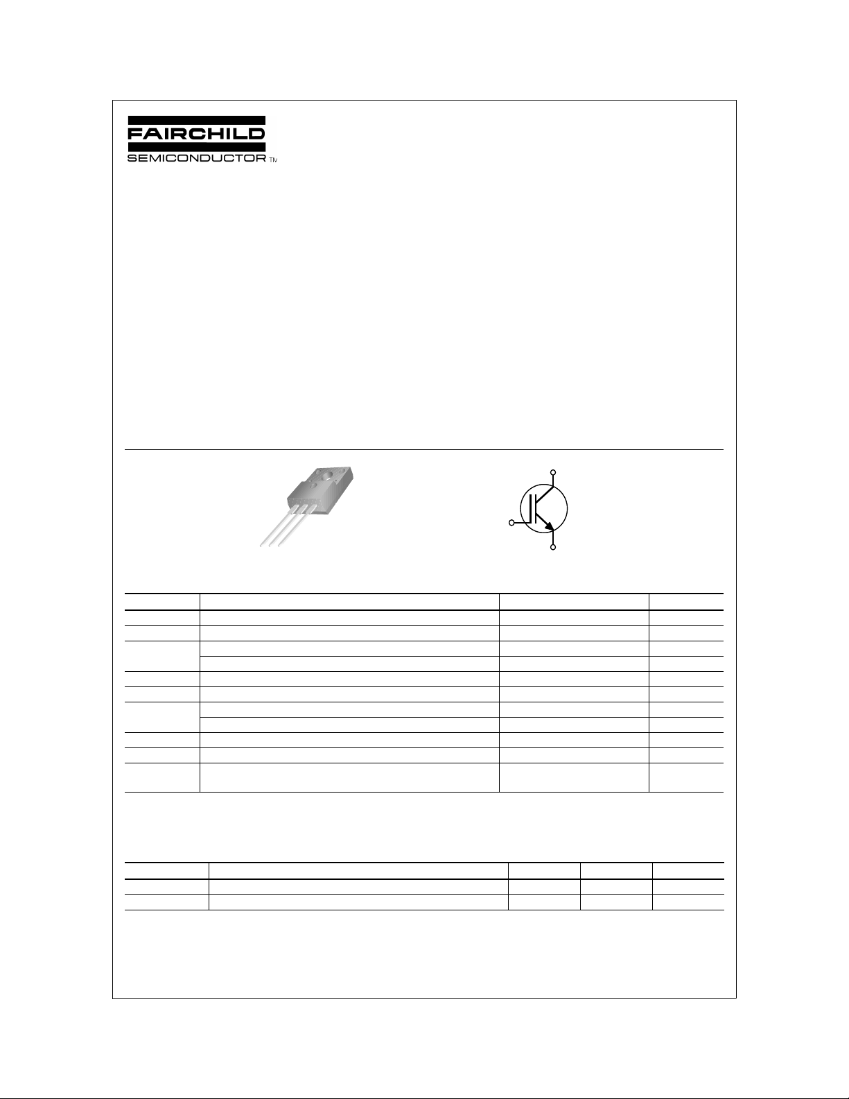
G C E
TO-220F
Features
• Short circuit rated 10us @ TC = 100°C, VGE = 15V
• High speed switching
• Low saturation voltage : V
• High input impedance
CE(sat)
C
C
G
G
E
E
IGBT
= 2.2 V @ IC = 5A
Absolute Maximum Ratings T
Symbol Description SGS5N60RUF Units
V
CES
V
GES
I
C
I
CM (1)
T
SC
P
D
Operating Junction Temperature -55 to +150 °C
T
J
T
stg
T
L
Notes :
(1) Repetitive rating : Pulse width limited by max. junction temperature
Collector-Emitter Voltage 600 V
Gate-Emitter Voltage ± 20 V
Collector Current @ TC = 25°C8 A
Collector Current @ T
Pulsed Collector Current 15 A
Short Circuit Withstand Time @ TC = 100°C10 µs
Maximum Power Dissipation @ TC = 25°C35 W
Maximum Power Dissipation @ T
Storage Temperature Range -55 to +150 °C
Maximum Lead Tem p. for soldering
purposes, 1/8” from Case for 5 Seconds
= 25°C unless otherwise noted
C
= 100°C5 A
C
= 100°C14 W
C
300 °C
Thermal Characteristics
Symbol Parameter Typ. Max. Units
R
θJC
R
θJA
Thermal Resistance, Junction-to-Case -- 3.5 °C/W
Thermal Resistance, Junction-to-Ambient -- 62.5 °C/W
©2001 Fairchild Semiconductor Corporation
SGS5N60RUF Rev. A
Page 2
SGS5N60RUF
Electrical Characteristics of IGBT T
= 25°C unless otherwise noted
C
Symbol Parameter Test Conditions Min. Typ. Max. Units
Off Characteristics
BV
∆B
∆T
I
CES
I
GES
CES
VCES
J
Collector-Emitter Breakdown Voltage VGE = 0V, IC = 250uA 600 -- -- V
/
Temperature Coeff. of Breakdown
Voltage
Collector Cut-off Current VCE = V
G-E Leakage Current VGE = V
V
= 0V, IC = 1mA -- 0.6 -- V/°C
GE
, VGE = 0V -- -- 250 µA
CES
, VCE = 0V -- -- ± 100 nA
GES
On Characteristics
V
GE(th)
V
CE(sat)
G-E Threshold Voltage IC = 5mA, VCE = V
,
= 5A
= 8A
VGE = 15V
,
VGE = 15V
Collector to Emitter
Saturation Voltage
I
C
I
C
GE
5.0 6.0 8.5 V
-- 2.2 2.8 V
-- 2.5 -- V
Dynamic Characteristics
C
ies
C
oes
C
res
Input Capacitance
Output Capacitance -- 67 -- pF
Reverse Transfer Capacitance -- 14 -- pF
= 30V, VGE = 0V,
V
CE
f = 1MHz
-- 354 -- pF
Switching Characteristics
t
d(on)
t
r
t
d(off)
t
f
E
on
E
off
E
Total Switching Loss -- 195 280 µJ
ts
t
d(on)
t
r
t
d(off)
t
f
E
on
E
off
Total Switching Loss -- 323 -- µJ
E
ts
T
sc
Q
g
Q
ge
Q
gc
Le Internal Emitter Inductance Measured 5mm from PKG -- 7.5 -- nH
Turn-On Delay Time
-- 13 -- ns
Rise Time -- 24 -- ns
Turn-Off Delay Time -- 34 50 nS
Fall Time -- 136 200 ns
Turn-On Switching Loss -- 88 -- µJ
V
= 300 V, IC = 5A,
CC
R
= 40Ω, V
G
GE
Inductive Load, T
= 15V,
= 25°C
C
Turn-Off Switching Loss -- 10 7 -- µJ
Turn-On Delay Time
-- 13 -- ns
Rise Time -- 26 -- ns
Turn-Off Delay Time -- 40 60 ns
Fall Time -- 250 350 ns
Turn-On Switching Loss -- 103 -- µJ
= 300 V, IC = 5A,
V
CC
= 40Ω, V
R
G
GE
Inductive Load, T
= 15V,
= 125°C
C
Turn-Off Switching Loss -- 22 0 -- µJ
Short Circuit Withstand Time
Total Gate Charge
Gate-Emitter Charge -- 3 6 nC
Gate-Collector Charge -- 7 14 nC
VCC = 300 V, V
@
TC = 100°C
= 300 V, IC = 5A,
V
CE
V
= 15V
GE
= 15V
GE
10 -- -- µs
-- 16 24 nC
©2001 Fairchild Semiconductor Corporation SGS5N60RUF Rev. A
Page 3
SGS5N60RUF
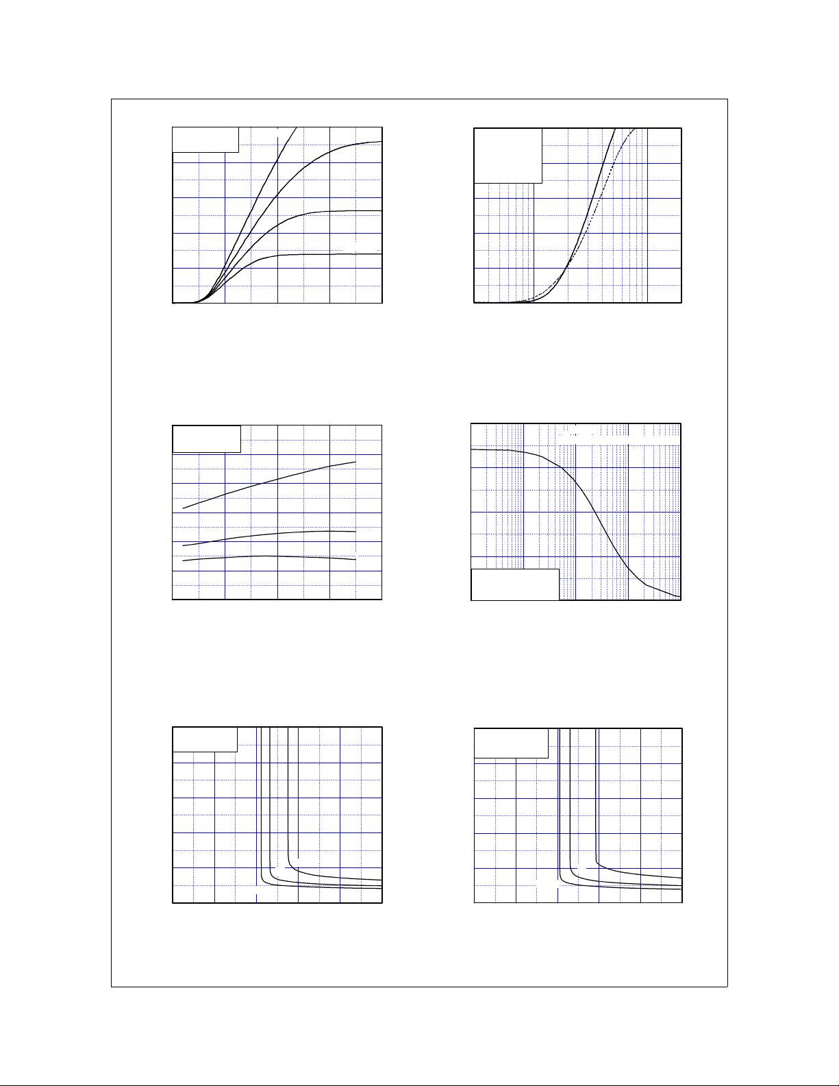
25
Common Emitter
℃
TC = 25
20
[A]
C
15
10
Collector Curren t, I
5
0
02468
20V
VGE = 10V
Colle c t or - Emitter Voltage, VCE [V]
Fig 1. Typical Output Chacracteristics
4.0
Common Emitter
V
= 15V
GE
3.5
[V]
CE
3.0
2.5
2.0
1.5
Collec tor - Emitter V oltage, V
1.0
-50 0 50 100 150
Case Temperature, TC [℃]
IC = 3A
10A
5A
15V
12V
20
Common Emitter
V
= 15V
GE
━━
T
= 25℃
16
C
T
= 125℃ ------
[A]
C
C
12
8
Collector Current, I
4
0
110
Collector - Emitter Voltage, VCE [V]
Fig 2. Typical Saturation Voltage
Characteristics
8
6
4
Load Current [A]
2
Duty cycle : 50%
℃
= 100
T
C
Power Dissipation = 9W
0
0.1 1 10 100 1000
VCC = 300V
Load Current : peak of square wave
Frequency [KHz]
Fig 3. Saturation Voltage vs. Case
Temperature at Variant Current Level
20
Common Emitter
℃
T
= 25
C
16
[V]
CE
12
8
4
Collector - Emitter Voltage, V
0
0 4 8 121620
IC = 3A
Gate - Emitter Voltage, VGE [V]
Fig 5. Saturation Voltage vs. V
©2001 Fairchild Semiconductor Corporation SGS5N60RUF Rev. A
10A
5A
GE
Fig 4. Load Current vs. Frequency
20
Common Emitter
℃
T
= 125
C
16
[V]
CE
12
8
4
Collector - Emitte r Vo l tage, V
0
0 4 8 12 16 20
IC = 3A
Gate - Emitter Voltage, VGE [V]
Fig 6. Saturation Voltage vs. V
10A
5A
GE
Page 4

SGS5N60RUF
700
600
500
400
300
Capacitance [pF]
200
100
0
110
Collector - Emitter Voltage, VCE [V]
Fig 7. Capaci tance Characterist ics
Common Emitter
V
= 300V, VGE = ±15V
CC
I
= 5A
C
━━
T
= 25℃
C
T
= 125℃ ------
C
Switching Time [ns]
100
10 100
Gate Resistance, RG [Ω]
Common E mitter
= 0V, f = 1MHz
V
GE
℃
T
= 25
C
Cies
Coes
Cres
Toff
Tf
Toff
Tf
Common Emitter
VCC = 300V, VGE = ±15V
IC = 5A
━━
TC = 25℃
TC = 125℃ ------
100
Switching Time [ns]
10
10 100
Gate Resistance, RG [Ω]
Fig 8. Turn-On Characteristics vs.
Gate Resistance
1000
100
Switching Loss [uJ]
10
10 100
Gate Resistance, RG [Ω]
Common Em itte r
V
= 300V, VGE = ±15V
CC
I
= 5A
C
= 25℃
T
C
T
= 125℃ ------
C
Ton
Tr
Eoff
Eon
Eoff
━━
Fig 9. Turn-Off Characteristics vs.
Fig 10. Switching Loss vs. Gate Resi st ance
Gate Resistance
Common Emitter
V
= ±15V, RG = 40Ω
GE
━━
TC = 25℃
T
= 125℃ ------
C
100
Ton
Tr
Switching Time [ns]
10
345678910
Collector Current, IC [A]
Fig 11. Turn-O n C har acteristics vs.
Collector Current
©2001 Fairchild Semiconductor Corporation SGS5N60RUF Rev. A
Common Emitter
V
= ±15V, RG = 40
GE
TC = 25℃
1000
T
= 125℃ ------
C
Toff
Tf
Switching Time [ns]
Toff
Tf
100
345678910
━━
Ω
Collecto r C u rrent, IC [A]
Fig 12. Turn-Off Characteristics vs.
Collector Current
Page 5

SGS5N60RUF
1000
Common Emitter
V
= ±15V, RG = 40Ω
GE
━━
TC = 25℃
= 125℃ ------
T
C
Eoff
100
Eon
Switching Loss [uJ]
345678910
Collector Curre n t, IC [A]
Fig 13. Switching Loss vs. Collector Current
50
IC MAX. (Pulsed)
10
IC MAX. (Continuous)
[A]
C
1
DC Operation
㎳
1
50us
100us
15
Common Em itte r
= 60Ω
R
L
℃
TC = 25
12
[V]
GE
9
6
3
Gate - Emitter Voltage, V
0
0 3 6 9 12 15 18
VCC = 100V
300V
200V
Gate Charge, Qg [nC]
Fig 14. Gate Charge Char ac te ri st ic s
40
[A]
C
10
0.1
Single Nonrepetitive
Collector Current, I
Pulse T
Curves must be derated
linearly w it h increas e
in temper at ur e
0.01
0.3 1 10 100 1000
= 25
C
℃
Collector-Emitter Voltage, VCE [V]
Fig 15. SOA Characteristic
10
0.5
/W]
℃
1
0.2
0.1
0.05
0.02
0.1
0.01
Thermal Respon se, Zth jc [
0.01
10
-5
single pulse
-4
10
Collector Current, I
1
1 10 100 1000
Fig 16. Turn-Off SOA Characteristics
-3
10
Rectangular Pulse Duration [s ec]
-2
10
Safe Operatin g A rea
VGE = 20V, TC = 100
Collector-Emitter Voltage, VCE [V]
Pdm
t1
t2
Duty factor D = t1 / t2
Peak Tj = Pdm × Zthjc + T
-1
10
0
10
℃
C
1
10
Fig 17. Transient Thermal Impedance of IGBT
©2001 Fairchild Semiconductor Corporation SGS5N60RUF Rev. A
Page 6

Package Dimension
TO-220F (FS PKG CODE AQ)
10.16 ±0.20
ø3.18 ±0.10
2.54
SGS5N60RUF
±0.20
3.30 ±0.10
15.80 ±0.20
9.75 ±0.30
MAX1.47
0.80 ±0.10
(7.00)
(30°)
6.68 ±0.20
(1.00x45°)
(0.70)
15.87 ±0.20
0.35 ±0.10
2.54TYP
[2.54
±0.20]
2.54TYP
[2.54
±0.20]
0.50
+0.10
–0.05
2.76 ±0.20
9.40 ±0.20
4.70 ±0.20
Dimensions in Millimeters
©2001 Fairchild Semiconductor Corporation SGS5N60RUF Rev. A
#1
Page 7

TRADEMARKS
The following are registered and unregistered trademarks Fairchild Semiconductor owns or is authorized to use and is not
intended to be an exhaustive list of all such trademarks.
ACEx™
Bottomless™
CoolFET™
CROSSVOLT™
DenseTrench™
DOME™
EcoSPARK™
2
E
CMOS™
EnSigna™
FACT™
FACT Quiet Series™
®
FAST
FASTr™
GlobalOptoisolator™
GTO™
HiSeC™
ISOPLANAR™
LittleFET™
MicroFET™
MICROWIRE™
OPTOLOGIC™
OPTOPLANAR™
PACMAN
™
POP™
PowerTrench
®
QFET™
QS™
QT Optoelectronics™
Quiet Series™
SLIENT SWITCHER
SMART START™
Star* Power™
Stealth™
SuperSOT™-3
SuperSOT™-6
SuperSOT™-8
SyncFET™
TinyLogic™
UHC™
UltraFET
®
VCX™
®
DISCLAIMER
FAIRCHILD SEMICONDUCTOR RESERVES THE RIGHT TO MAKE CHANGES WITHOUT FURTHER NOTICE TO ANY
PRODUCTS HEREIN TO IMPROVE RELIABILITY, FUNCTION OR DESIGN. FAIRCHILD DOES NOT ASSUME ANY
LIABILITY ARISING OUT OF THE APPLICATION OR USE OF ANY PRODUCT OR CIRCUIT DESCRIBED HEREIN;
NEITHER DOES IT CONVEY ANY LICENSE UNDER ITS PATENT RIGHTS, NOR THE RIGHTS OF OTHERS.
LIFE SUPPORT POLICY
FAIRCHILD’S PRODUCTS ARE NOT AUTHORIZED FOR USE AS CRITICAL COMPONENTS IN LIFE SUPPORT
DEVICES OR SYSTEMS WITHOUT THE EXPRESS WRITTEN APPROVAL OF FAIRCHILD SEMICONDUCTOR
CORPORATION.
As used herein:
1. Life support devices or systems are devices or systems
which, (a) are intended for surgical implant into the body,
or (b) support or sustain life, or (c) whose failure to perform
when properly used in accordance with instructions for use
provided in the labeling, can be reasonably expected to
result in significant injury to the user.
2. A critical component is any component of a life support
device or system whose failure to perform can be
reasonably expected to cause the failure of the life support
device or system, or to affect its safety or effectiveness.
PRODUCT STATUS DEFINITIONS
Definition of Terms
Datasheet Identification Product Sta tus Definition
Advance Information Formative or In
Design
Preliminary First Production This datasheet contains preliminary data, and
No Identification Needed Full Production This datasheet contains final specifications. Fairchild
Obsolete Not In Production This datasheet contains specifications on a product
©2001 Fairchild Semiconductor Corporation
This datasheet contains the design specifications for
product development. Specifications may change in
any manner without notice.
supplementary data will be published at a later date.
Fairchild Semiconductor reserves the right to make
changes at any time without notice in order to improve
design.
Semiconductor reserves the right to make changes at
any time without notice in order to improve design.
that has been discontinued by Fairchild semiconductor.
The datasheet is printed for reference information only.
Rev. H1
 Loading...