

Datasheet SGR117AIG, SGR117AIG-883B, SGR117AK, SGR117AK-883B, SGR117AR Datasheet (Microsemi Corporation)
...Page 1
SGR117A
ADVANCED DATA SHEET
RAD HARD 1.5 AMP THREE TERMINAL
ADJUSTABLE VOLTAGE REGULATOR
DESCRIPTION
The RAD HARD SGR117A 3-terminal positive adjustable
regulators have been designed to meet the most stringent
space and strategic level radiation requirements while meeting
the industry standard LM117A and LM117 electrical
specifications.
In addition to the features of the standard SGR117A, these
devices are capable of meeting the attached data sheet
electricals after the following radiation events:
TOTAL DOSE: EXCEEDS 1 MEG RAD
NEUTRON FLUENCE: 5x10
12
N/cm²
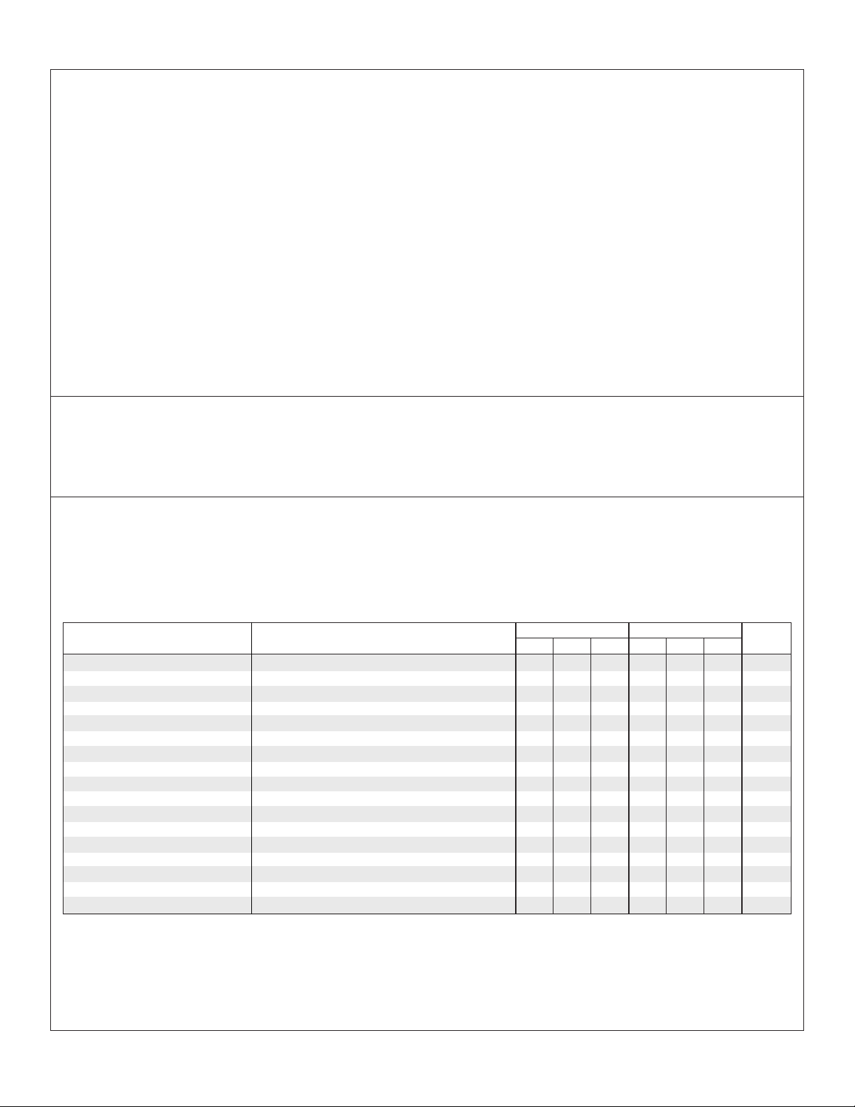
SCHEMATIC DIAGRAM
FEATURES
••
• Full electrical performance after radiation exposure
••
1 MEG Rad Total Dose
12
5x10
N/cm²
••
• 1% output voltage tolerance
••
••
• 0.01%/V line regulation
••
••
• 0.3% load regulation
••
••
• Min. 1.5A output current
••
••
• Available in TO-257 Package (Hermetic TO-220)
••
HIGH RELIABILITY FEATURES-SGR117A
♦♦
♦ Radiation data available
♦♦
♦♦
♦ Available to MIL-STD-883
♦♦
♦♦
♦ LMI level "S" processing available
♦♦
3/91 Rev 1.2 1/95 LINFINITY Microelectronics Inc.
Copyright 1994 11861 Western Avenue
1 (714) 898-8121
∞ ∞
∞ Garden Grove, CA 92841
∞ ∞
∞∞
∞ FAX: (714) 893-2570
∞∞
Page 2
ABSOLUTE MAXIMUM RATINGS (Note 1)
Power Dissipation .......................................
Input to Output Voltage Differential ..................................
Storage Temperature Range .........................
Note 1. Exceeding these ratings could cause damage to the device.
Internally Limited
40V
-65°C to 150°C
Operating Junction Temperature
Hermetic (K, R, T, IG-Packages) ....................................
Lead Temperature (Soldering, 10 Seconds) ..............
THERMAL DATA
K Package:
Thermal ResistanceThermal Resistance-
R Package:
Thermal ResistanceThermal Resistance-
T Package:
Thermal ResistanceThermal Resistance-
IG Package:
Thermal ResistanceThermal Resistance-
Junction to Case, θ
Junction to Ambient, θ
Junction to Case, θ
Junction to Ambient, θ
Junction to Case, θ
Junction to Ambient, θ
Junction to Case, θ
Junction to Ambient, θ
JC
JC
JC
JC
................. 3.0°C/W
.............. 35°C/W
JA
................. 5.0°C/W
............. 40°C/W
JA
.................. 15°C/W
........... 120°C/W
JA
................. 3.5°C/W
............. 42°C/W
JA
Note A. Junction Temperature Calculation: TJ = TA + (PD x θJA).
Note B. The above numbers for θ
RECOMMENDED OPERATING CONDITIONS (Note 2 & 3)
Input Voltage Range ................................. (V
Note 2. Range over which the device is functional.
Note 3. These ratings are applicable for junction temperatures of less than 150°C.
+ 3.5V) to 37V Operating Junction Temperature Range
OUT
SGR117A ........................................................-55°C to 150°C
SGR117A
150°C
300°C
are maximums for the limiting
thermal resistance of the package in a standard mounting configuration. The θ
guidelines for the thermal performance of the device/pcboard system. All of the above assume no ambient
airflow.
JC
numbers are meant to be
JA
ELECTRICAL CHARACTERISTICS
(Unless otherwise specified, these specifications apply over full operating ambient temperatures for SGR117 with -55°C ≤ TA ≤ 125°C, VIN - V
5.0V, and for I
for power dissipations of 2W for the T package, and 20W for the K and IG packages. I
Low duty cycle pulse testing techniques are used which maintains junction and case temperatures equal to the ambient temperature.)
Reference Voltage
Line Regulation
Load Regulation (Note 4)
Thermal Regulation (Note 5)
Ripple Rejection
Adjust Pin Current
Adjust Pin Current Change
= 500mA (K and IG), and I
OUT
= 100mA (T package). Although power dissipation is internally limited, these specifications are applicable
OUT
Parameter Test Conditions
I
= 10mA TA = 25°C
(Note 4)
OUT
3V ≤ (V
10mA ≤ I
3V ≤ (VIN - V
T
T
10mA ≤ I
V
V
V
V
T
V
C
C
10mA ≤ I
- V
IN
= 25°C
A
= T
A
MIN
≤ 5V, TA = 25°C
OUT
≥ 5V, TA = 25°C
OUT
≤ 5V
OUT
≥ 5V
OUT
= 25°C, 20ms pulse
A
= 10V, f =120Hz
OUT
= 1µF, TA = 25°C
ADJ
= 10µF
ADJ
) ≤ 40V, P ≤ P
OUT
≤ I
OUT
MAX
) ≤ 40V, IL = 10mA
OUT
to T
MAX
≤ I
OUT
MAX
≤ I
OUT
, 2.5V ≤ (VIN - V
MAX
MAX
,
is 1.5A for the K and IG packages and 500mA for the T package.
MAX
POST NEUTRON
5 x 10¹² N/cm²
SGR117A
Min. Typ. Max.
1.220
1.220
15
50
1
66
5
1.25
0.01
0.02
5
0.1
20
0.3
0.03
65
80
50
0.2
OUT
) ≤ 40V
PRE RAD
SGR117A
Min. Typ. Max.
1.250
1.250
0.005
0.01
1.262
1.270
0.01
0.02
1.238
1.225
5
0.3
0.1
20
0.3
0.02
0.002
65
80
66
100
50
0.2
Units
1.275
1.275
0.03
0.05
50
1
50
1
0.07
100
8
OUT
V
V
%/V
%/V
mV
%
mV
%
%/W
dB
dB
µA
µA
=
3/91 Rev 1.2 1/95 LINFINITY Microelectronics Inc.
Copyright 1994 11861 Western Avenue
2 (714) 898-8121
∞ ∞
∞ Garden Grove, CA 92841
∞ ∞
∞∞
∞ FAX: (714) 893-2570
∞∞
Page 3

SGR117A
ELECTRICAL CHARACTERISTICS (continued)
Test ConditionsParameter
Minimum Load Current
Current Limit
Temperature Stability (Note 5)
Long Term Stability (Note 5)
RMS Output Noise (% of V
OUT
(VIN - V
(V
K, R, IG Packages
IN
- V
OUT
OUT
) = 40V
) ≤ 15V
T Package
(V
- V
) = 40V, TJ = 25°C
IN
OUT
K, R, IG Packages
T Package
= 125°C, 1000 Hours
T
A
T
= 25°C, 10Hz ≤ f ≤ 10 KHz (Note 5)
)
A
PRE RAD
SGR117A
1.5
0.5
0.3
0.15
3.5
2.2
0.8
0.4
0.2
1
0.3
0.001
POST NEUTRON
5 x 10¹² N/cm²
SGR117A
Min. Typ. Max.Min. Typ. Max.
5
1.5
0.5
0.3
0.15
2
1
3.5
2.2
0.8
0.4
0.2
Units
8mA
Note4. Regulation is measured at constant junction temperature, using pulse testing with a low duty cycle. Changes in output voltage due to
heating effects are covered under the specification for thermal regulation.
Note 5. These parameters, although guaranteed, are not tested in production.
CONNECTION DIAGRAMS & ORDERING INFORMATION (See Notes Below)
Ambient
Temperature Range
Connection Diagram
ADJUSTMENT
1
3-TERMINAL TO-3
METAL CAN
K-PACKAGE
Part No.Package
SGR117AK -55°C to 125°C
SGR117AK/883B -55°C to 125°C
A
A
A
A
%
%
%
3-TERMINAL TO-66
METAL CAN
R-PACKAGE
3-PIN TO-39 METAL CAN
T-PACKAGE
3-PIN HERMETIC TO-257
IG-PACKAGE (Isolated)
SGR117AR -55°C to 125°C
SGR117AR/883B -55°C to 125°C
SGR117AT -55°C to 125°C
SGR117AT/883B -55°C to 125°C
SGR117AIG/883B -55°C to 125°C
SGR117AIG -55°C to 125°C
V
IN
ADJUSTMENT
V
IN
IN
ADJUST 32
CASE IS V
(TAB IS V
FOR G-PACKAGE ONLY
)
OUT
2
CASE IS V
OUT
1
2
CASE IS V
OUT
1V
V
OUT
OUT
V
IN
V
OUT
ADJUST
Note 1. Contact factory for JAN and DESC product availability.
2. All parts are viewed from the top.
3/91 Rev 1.2 1/95 LINFINITY Microelectronics Inc.
Copyright 1994 11861 Western Avenue
3 (714) 898-8121
∞ ∞
∞ Garden Grove, CA 92841
∞ ∞
∞∞
∞ FAX: (714) 893-2570
∞∞
 Loading...