

Page 1
SGF15N90D
SGF15N90D
General Description
Insulated Gate Bipolar Transistors (IGBTs) with a trench
gate structure provide superior conduction and switching
performance in comparison with transistors having a planar
gate structure. They also have wide noise immunity. These
devices are very suitable for induction heating applications.
Applications
Home appliances, induction heaters, induction hea 1 ting JARs, and microwave ovens.
TO-3PF
C
Features
• High speed switching
• Low saturation voltage : V
• High input impedance
• Built-in fast recovery diode
G
G
= 2.0 V @ IC = 15A
CE(sat)
C
C
E
E
IGBT
Absolute Maximum Ratings T
Symbol Description SGF15N90D Units
V
CES
V
GES
I
C
I
CM (1)
I
F
P
D
Operating Junction Temperature -55 to +150 °C
T
J
T
stg
T
L
Notes :
(1) Repetitive rating : Pulse width limited by max. junction temperature
Collector-Emitter Voltage 900 V
Gate-Emitter Voltage ± 25 V
Collector Current @ TC = 25°C15 A
Collector Current @ T
Pulsed Collector Current 30 A
Diode Continuous Forward Current @ TC = 100°C12 A
M a x i m u m P o w e r D i s s i p a t i o n @ TC = 25°C83 W
Maximum Power Dissipation @ T
Storage Temperature Range -55 to +150 °C
Maximum Lead Tem p. for soldering
purposes,1/8” from case for 5 seconds
= 25°C unless otherwise noted
C
= 100°C12 A
C
= 100°C33 W
C
300 °C
Thermal Characteristics
Symbol Parameter Typ. Max. Units
R
(IGBT) Thermal Resistance, Junction-to-Case -- 1.5 °C/W
θJC
(DIODE) Thermal Resistance, Junction-to-Case -- 2.86 °C/W
R
θJC
R
θJA
Thermal Resistance, Junction-to-Ambient -- 40 °C/W
©2002 Fairchild Semiconductor Corporation SGF15N90D Rev. A1
Page 2
SGF15N90D
Electrical Characteristics of the IGBT T
= 25°C unless otherwise noted
C
Symbol Parameter Test Conditions Min. Typ. Max. Units
Off Characteristics
BV
I
CES
I
GES
CES
Collector-Emitter Breakdown Voltage VGE = 0V, IC = 250µA 900 -- -- V
Collector Cut-off Current VCE = V
G-E Leakage Current VGE = V
, VGE = 0V -- -- 1.0 mA
CES
, VCE = 0V -- -- ± 500 nA
GES
On Characteristics
V
GE(th)
V
CE(sat)
G-E Threshold Voltage IC = 15mA, VCE = V
,
Collector to Emitter
Saturation Voltage
I
C
I
C
= 2.5A
= 15A
VGE = 15V
,
VGE = 15V
GE
4.0 5.0 7.0 V
-- 1.4 1.8 V
-- 2.0 2.7 V
Dynamic Characteristics
C
ies
C
oes
C
res
Input Capacitance
Output Capacitance -- 80 -- pF
Reverse Transfer Capacitance -- 50 -- pF
=10V, VGE = 0V,
V
CE
f = 1MHz
-- 1500 -- pF
Switching Characteristics
t
d(on)
t
r
t
d(off)
t
f
Q
Q
Q
g
ge
gc
Turn-On Delay Time
Rise Time -- 180 280 ns
Turn-Off Delay Time -- 150 230 ns
Fall Time -- 200 320 ns
Total Gate Charge
Gate-Emitter Charge -- 15 -- nC
Gate-Collector Charge -- 20 -- nC
= 600 V, IC = 15A,
V
CC
= 51Ω, V
R
G
Resistive Load, T
= 600 V, IC = 15A,
V
CE
V
GE
= 15V
GE
= 15V,
25°C
C
-- 50 80 ns
-- 60 80 nC
Electrical Characteristics of DIODE T
= 25°C unless otherwise noted
C
Symbol Parameter Test Conditions Min. Typ. Max. Units
I
= 4A -- 1.1 1.6 V
V
FM
t
rr
I
R
Diode Forward Voltage
Diode Reverse Recovery Time IF = 15A, di/dt = 20 A/µs
Instantaneous Reverse Current V
F
I
= 15A -- 1.45 1.7 V
F
RRM
= 900V -- 0.03 1.2 uA
-- 0.8 1.2 us
©2002 Fairchild Semiconductor Corporation
SGF15N90D Rev. A1
Page 3
SGF15N90D
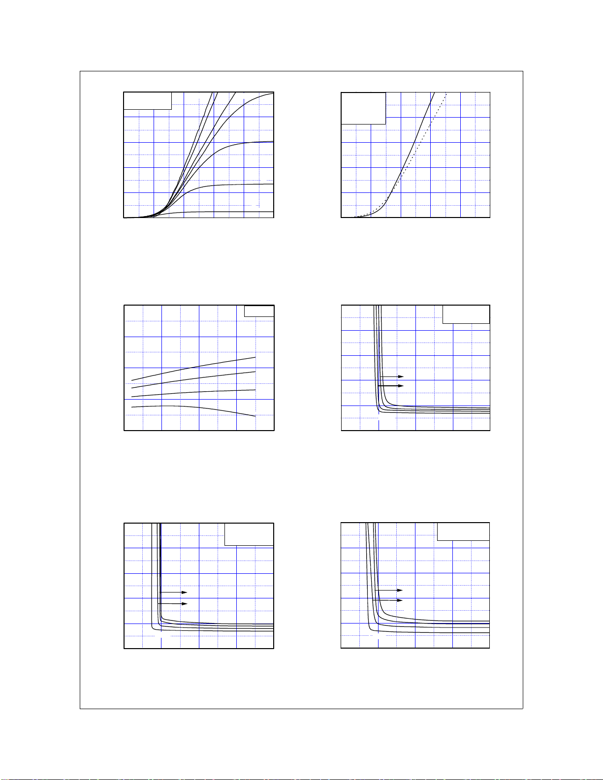
50
Common Emitter
℃
= 25
T
C
40
[A]
C
30
20
Collecto r Current, I
10
0
012345
20V
15V 10V
9V
7V
VGE = 6V
Collector-Emitter Voltage, VCE [V]
Fig 1. Typical Output Characteristics
3.0
[V]
2.5
CE
2.0
1.5
Collector-Emitter Voltage , V
1.0
-50 0 50 100 150
Case Temperature, TC [℃]
VGE = 15V
20A
15A
10A
IC = 5A
50
Common Emitter
= 15V
V
GE
━━
= 25℃
T
C
40
T
= 125℃ ------
C
[A]
8V
C
30
20
Collector Current, I
10
0
012345
Collector-Emitter Voltage,VCE [V]
Fig 2. Typical Saturation V oltage Characteristics
10
8
[V]
CE
6
4
2
Collector-Emitter Voltage, V
0
4 8 12 16 20
15A
10A
20A
IC = 5A
Common Emitter
℃
= -40
T
C
Gate-Emitter Voltage, VGE [V]
Fig 3. Saturation Voltage vs. Case
Temperature at Variant Current Level
10
8
[V]
CE
6
4
2
Collector-Emitter Voltage, V
0
4 8 12 16 20
IC = 5A
15A
10A
20A
Gate-Emitter Voltage, VGE [V]
Fig 5. Saturation Voltage vs. V
©2002 Fairchild Semiconductor Corporation
Common Emitter
℃
= 25
T
C
GE
Fig 4. Saturation Voltage vs. V
10
8
[V]
CE
6
4
2
Collector-Emitter Voltage, V
0
4 8 12 16 20
IC = 5A
15A
10A
20A
GE
Common Emitter
= 125
T
C
Gate-Emitter Voltage, VGE [V]
Fig 6. Saturation Voltage vs. V
GE
℃
SGF15N90D Rev. A1
Page 4

SGF15N90D
2000
Cies
1000
Capacitance [pF]
Coes
Cres
110
Common Emitter
= 0V, f = 1MHz
V
GE
℃
T
= 25
C
Collector-Emitter Voltage, VCE [V]
Fig 7. Capaci tance Characterist ics
1000
Tf
Tdoff
100
Tr
Switching Time [ns]
Tdon
10
03691215
Collector Current,Ic [A ]
VCC=600V
Ω
RG=51
VGE=±15V
℃
TC=25
10000
1000
Tf
Tr
100
Switching Tim e [n s]
Toff
Ton
10
0 50 100 150 200
VCC = 600V
= 15A
I
C
= ±15V
V
GE
℃
= 25
T
C
Gate Resistance, RG [Ω]
Fig 8. Switching Charac te ri st i cs vs .
Gate Resistance
15
Common Emitter
= 600V, RL = 40
V
CC
℃
= 25
T
C
12
[V]
GE
9
6
3
Gate-Emitter Voltage, V
0
0 20406080
Ω
Gate Charge, Qg [nC]
Fig 9. Switching Characteristics vs.
Collector current
100
IC MAX. (Pulsed)
IC MAX. (Continuous)
10
[A]
C
1
Single Nonrepetitive Pulse
0.1
Collector Current ,I
0.01
℃
= 25
T
C
Curve must be dara t ed
linearly with increase
in temperature
1 10 100 1000
DC Operati o n
Collector-Emitter Voltage, V
Fig 11. SOA Characteristics
©2002 Fairchild Semiconductor Corporation
Fig 10. Gate Charge Characteristics
10
C/W]
1
0.5
o
0.2
0.1
0.05
0.1
0.02
0.01
Therma l Response, Zth jc [
0.01
single pulse
10-510-410-310-210-110010
Pdm
t1
t2
Duty factor D = t1 / t2
Peak Tj = Pdm
Rectangular Pulse Duration [sec]
Zthjc + T
×
C
1
10ms
100us
1ms
[V]
CE
Fig 12. Transient Thermal Impedance of IGBT
SGF15N90D Rev. A1
Page 5

SGF15N90D
30
━━
TC = 25℃
TC = 100℃ ------
10
[A]
F
1
Forward Current, I
0.1
0.0 0.5 1.0 1.5 2.0 2.5
Forward Voltage, VFM [V]
1.2
di/dt = 20A/us
℃
= 25
T
C
1.0
[us]
rr
0.8
0.6
0.4
0.2
Reverse Recovery Time, t
0.0
0 5 10 15 20
t
rr
I
rr
Forwa rd Current, IF [A]
1.0
0.9
0.8
[us]
rr
0.7
0.6
0.5
0.4
0.3
0.2
Reverse Recovery Time, t
0.1
0.0
04080120160200
t
rr
I
rr
IF = 15A
TC = 25
100
90
℃
Reverse Recovery Current, I
80
70
60
50
40
30
20
rr
[A]
10
0
di/dt [A/us]
Fig 14. Reverse Recovery Characte ristics vs. di/dtFig 13. Forward Characteristics
12
Reverse Recovery Current, I
10
8
6
4
rr
[A]
2
0
1000
100
[uA]
R
10
1
Reverse Current, I
0.1
0.01
0 300 600 900
TC = 25℃
= 150℃ ------
T
C
━━
Reverse Voltage, VR [V]
Fig 15. Reverse Reco very Characterist ic s
vs. Forward current
100
80
[pF]
j
60
40
20
Junction Capacitance, C
0
0.1 1 10 100
Reverse Voltage, VR [V]
Fig 17. Junction Capacitance
©2002 Fairchild Semiconductor Corporation
TC = 25
Fig 16. Reverse Current vs. Reverse Voltage
℃
SGF15N90D Rev. A1
Page 6

Package Dimension
SGF15N90D
TO-3PF
5.50 ±0.20
26.50 ±0.20
4.50 ±0.20
14.50 ±0.20
16.50 ±0.20
2.00 ±0.20
2.00 ±0.20
4.00 ±0.20
2.00 ±0.20
15.50 ±0.20
ø3.60 ±0.20
2.50 ±0.20
2.00 ±0.20
10.00 ±0.20
0.85 ±0.03
16.50 ±0.20
3.00 ±0.20
(1.50)
10°
23.00 ±0.20
22.00 ±0.20
1.50 ±0.20
2.00 ±0.20
3.30
14.80 ±0.20
©2002 Fairchild Semiconductor Corporation SGF15N90D Rev. A1
0.75
5.45TYP
[5.45
±0.30]
3.30 ±0.20
+0.20
–0.10
2.00 ±0.20
5.45TYP
[5.45
±0.30]
5.50 ±0.20
0.90
±0.20
+0.20
–0.10
Dimensions in Millimeters
Page 7

TRADEMARKS
The following are registered and unregistered trademarks Fairchild Semiconductor owns or is authorized to use and is not
intended to be an exhaustive list of all such trademarks.
®
ACEx™
Bottomless™
CoolFET™
CROSSVOLT™
DenseTrench™
DOME™
EcoSPARK™
2
CMOS™
E
EnSigna™
FACT™
FACT Quiet Series™
STAR*POWER is used under license
FAST
FASTr™
FRFET™
GlobalOptoisolator™
GTO™
HiSeC™
2
C™
I
ISOPLANAR™
LittleFET™
MicroFET™
MicroPak™
MICROWIRE™
OPTOLOGIC™
OPTOPLANAR™
PACMAN™
POP™
Power247™
PowerTrench
®
QFET™
QS™
QT Optoelectronics™
Quiet Series™
SLIENT SWITCHER
SMART START™
SPM™
STAR*POWER™
Stealth™
SuperSOT™-3
SuperSOT™-6
SuperSOT™-8
SyncFET™
TinyLogic™
TruTranslation™
®
UHC™
UltraFET
VCX™
DISCLAIMER
FAIRCHILD SEMICONDUCTOR RESERVES THE RIGHT TO MAKE CHANGES WITHOUT FURTHER NOTICE TO ANY
PRODUCTS HEREIN TO IMPROVE RELIABILITY, FUNCTION OR DESIGN. FAIRCHILD DOES NOT ASSUME ANY
LIABILITY ARISING OUT OF THE APPLICATION OR USE OF ANY PRODUCT OR CIRCUIT DESCRIBED HEREIN;
NEITHER DOES IT CONVEY ANY LICENSE UNDER ITS PATENT RIGHTS, NOR THE RIGHTS OF OTHERS.
LIFE SUPPORT POLICY
FAIRCHILD’S PRODUCTS ARE NOT AUTHORIZED FOR USE AS CRITICAL COMPONENTS IN LIFE SUPPORT
DEVICES OR SYSTEMS WITHOUT THE EXPRESS WRITTEN APPROVAL OF FAIRCHILD SEMICONDUCTOR
CORPORATION.
As used herein:
1. Life support devices or systems are devices or systems
which, (a) are intended for surgical implant into the body,
or (b) support or sustain life, or (c) whose failure to perform
when properly used in accordance with instructions for use
provided in the labeling, can be reasonably expected to
result in significant injury to the user.
2. A critical component is any component of a life support
device or system whose failure to perform can be
reasonably expected to cause the failure of the life support
device or system, or to affect its safety or effectiveness.
®
PRODUCT STATUS DEFINITIONS
Definition of Terms
Datasheet Identification Product Status Definition
Advance Information Formative or In
Design
Preliminary First Production This datasheet contains preliminary data, and
No Identification Needed Full Production This datasheet contains final specifications. Fairchild
Obsolete Not In Production This datasheet contains specifications on a product
This datasheet contains the design specifications for
product development. Specifications may change in
any manner without notice.
supplementary data will be published at a later date.
Fairchild Semiconductor reserves the right to make
changes at any time without notice in order to improve
design.
Semiconductor reserves the right to make changes at
any time without notice in order to improve design.
that has been discontinued by Fairchild semiconductor.
The datasheet is printed for reference information only.
Rev. H5©2002 Fairchild Semiconductor Corporation
 Loading...