

Page 1
Murata
Manufacturing Co., Ltd.
Please read CAUTION and Notice in this catalog for safety. This catalog has only typical specifications. Therefore you are requested
to approve our product specification or to transact the approval sheet for product specification, before your ordering.
Ceramic Filters (CERAFILr) for FM Receivers
CERAMIC
FILTERS
P61E7.pdf 01.10.17
(CERAFILr)
Cat.No.P61E-7
Page 2
Please read CAUTION and Notice in this catalog for safety. This catalog has only typical specifications. Therefore you are requested
to approve our product specification or to transact the approval sheet for product specification, before your ordering.
P61E7.pdf 01.10.17
CONTENTS
Part Numbering 2
1
CERAFILr Chip Type SFECV Series 3
Chip CERAFILr SFECV Series Notice 6
2
CERAFILr Small Chip Type SFECS Series 7
Chip CERAFILr SFECS Series Notice 10
3
CERAFILr Standard Lead Type 11
4
CERAFILr Low-loss Type 14
5
CERAFILr Low-profile Type 17
6
CERAFILr Lower Spurious Response Type 20
7
CERAFILr Wider Band-width Type 23
8
CERAFILr Narrow Band Type 25
CERAFILr and "CERAFIL" in this catalog are
the trademarks of Murata Manufacturing Co., Ltd.
1
2
3
4
5
6
7
9
CERAFILr For FM -IF Tuners 28
10
CERAFILr Three-Elements Type SFTLA Series 33
Lead Type CERAFILr Test Circuit and Characteristics Data 36
Lead Type CERAFILr Characteristics Data and Notice 37
11
Discriminators Chip Type CDACV Series 38
Chip Type Discriminators CDACV Series Notice 41
12
Discriminators Chip Low-profile Type CDSCA Series 42
Chip Type Discriminators CDSCA Series Notice 44
13
Discriminators CDALA Series 45
Lead Type Discriminators Notice 49
Packaging 50
Test Circuit of Ceramic Discriminator 53
Example of Appllied Circuit 54
8
9
10
11
12
13
Recycled Paper
Page 3
Please read CAUTION and Notice in this catalog for safety. This catalog has only typical specifications. Therefore you are requested
to approve our product specification or to transact the approval sheet for product specification, before your ordering.
P61E7.pdf 01.10.17
o Part Numbering
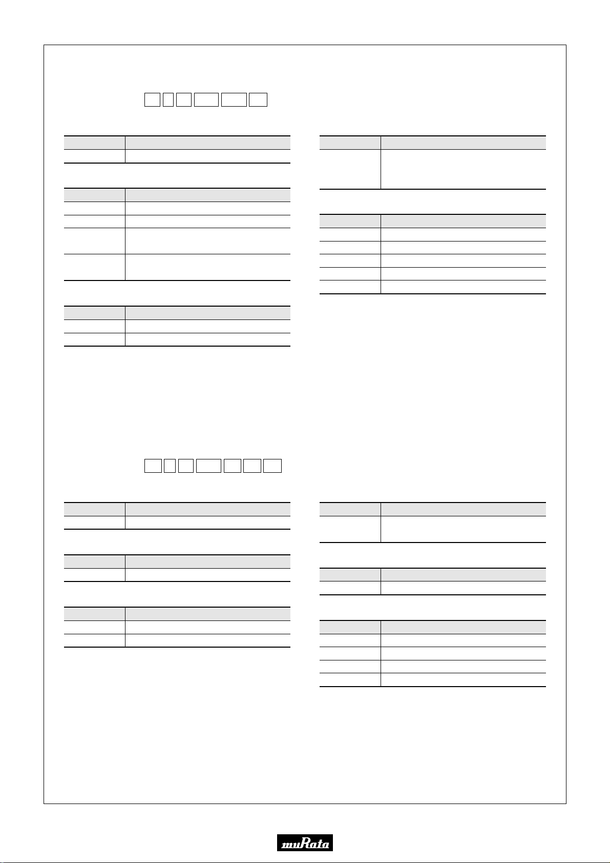
The structure of the "Global Part Numbers" that have been adopted since June 2001 and the meaning of each code are described herein.
()
If you have any questions about details, inquire at your usual Murata sales office or distributor.
CERAFILr for FM
E
(Global Part Number)
SF
q
w
qProduct ID
Product ID
SF Ceramic Filters
wOscillation/Numbers of Element
Code
E
T
K
V
Oscillation/Numbers of Element
2 Elements Thickness Expander mode
3 Elements Thickness Expander mode
2 Elements Thickness Expander mode
2 Elements Thickness Expander mode
eStructure/Size
Code
Lp
Cp
is expressed "A" or subsequent code, which indicates the size.
p
10M7tFAA0
LA
r
e
(2nd Harmonic)
(3rd Over Tone)
Structure/Size
Lead Type
Chip Type
-R0
y
tProduct Specification
Code
Product Specification
Four-digit alphanumerics express
FAA0
pass-bandwidth, center frequency tolerance,
rank, series, others.
yPackaging
Code
-B0
-R0
-R1
-A0
-A1
Radial taping is applied to lead type and plastic taping to chip type.
With non-standard products, two-digit alphanumerics indicating
"Individual Specification" is added between "tProduct Specification"
and "yPackaging".
1500pcs. /Radial Taping H
1000pcs. /Radial Taping H
Packaging
Bulk
Plastic Taping ø180mm
Plastic Taping ø330mm
0
0
=18mm
=18mm
rNominal Center Frequency
Expressed by four-digit alphanumerics. The unit is in hertz (MHz).
Decimal point is expressed by capital letter "M".
Discriminators for FM
-R0
(Global Part Number)
CD
q
A
w
e
10M7tGA
r
LA
qProduct ID
Product ID
CD Discriminators
wOscillation
Code
A
Oscillation
Thickness Expander mode
eStructure/Size
Code
Lp
Cp
is expressed "A" or subsequent code, which indicates the size.
p
Structure/Size
Lead Type
Chip Type
rNominal Center Frequency
Expressed by four-digit alphanumerics . The unit is in hertz (MHz).
Decimal point is expressed by capital letter "M".
001
y
u
tProduct Specification
Code
GA
Product Specification
Two-digit alphanumerics express
type, center frequency, rank, others
yIC
Code
001
Applicable IC Control Code
IC
uPackaging
Code
-B0
-A0
-R0
-R1
Radial taping is applied to lead type and plastic taping to chip type.
With non-standard products, an alphanumerics indicating "Individual
Specification" is added between "yIC" and "uPackaging".
Packaging
Bulk
Radial Taping H
=18mm
0
Plastic Taping (ø180mm)
Plastic Taping (ø330mm)
2
Page 4
Please read CAUTION and Notice in this catalog for safety. This catalog has only typical specifications. Therefore you are requested
to approve our product specification or to transact the approval sheet for product specification, before your ordering.
P61E7.pdf 01.10.17
Ceramic Filters (CERAFILr) for FM Receivers
CERAFILr Chip Type SFECV Series
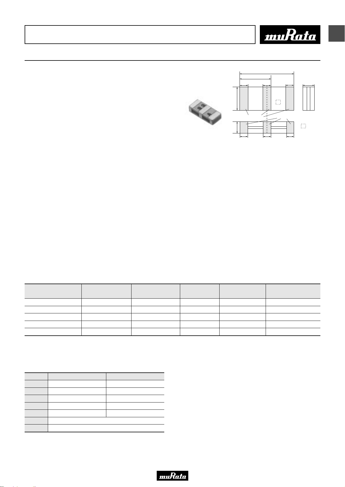
SFECV10M7 series for FM-receivers are monolithic type
ceramic filters which utilize the energy trapped
thickness vibration-mode of the piezoelectric ceramic.
By taking advantage of the very low profile, new SFECV
series and PFWCC(kHz filter for AM receiver) enable
costomers to make AM/FM set so thin, and it can be of
help to the total chip circuit.
■ Features
1. Super-thin. Only 1.5mm. The most suitable ceramic
filter available for thinning substrates.
2. Heat resistant. Reflow soldering can be performed
because of its excellent heat resistance.
3. Piezoelectric element is connected in the
sandwich shape by heat resistant substrate, thus
it has excellent mechanical strength, and it is
suitable for automatic mounting.
4. Various bandwidths are available. Select a
suitable type in accordance with the desired
selectivity.
5. Electrical characteristics are the same as
conventional "CERAFIL".
6.9±0.3
4.05±0.4
1.2±0.5
2.9±0.31.5±0.2
(3) (2) (1)
Bottom Electrode
1.0±0.5 1.0±0.5
** : EIAJ Monthly Code
** : Center Frequency Rank Code
1.2±0.3
*
*
*
1.0±0.5
1.2±0.5
Side Electrode
1.5±0.2
: Marking
(1) : Input
(2) : Ground
(3) : Output
(in mm)
1
■ Applications
1. Small, thin radios
2. Automotive radios
3. Headphone steros
Part Number
SFECV10M7KA00-R0 10.700 ±30kHz within110 ±30kHz 320 max. within6.0 ±2.0dB 35 min.
SFECV10M7JA00-R0 10.700 ±30kHz within150 ±40kHz 380 max. 10.0 max. 30 min.
SFECV10M7HA00-R0 10.700 ±30kHz within180 ±40kHz 470 max. within4.0 ±2.0 dB 35 min.
SFECV10M7GA00-R0 10.700 ±30kHz within230 ±50kHz 510 max. within3.5 ±2.0 dB 35 min.
SFECV10M7FA00-R0 10.700 ±30kHz within280 ±50kHz 590 max. within3.0 ±2.0 dB 35 min.
Area of Attenuation : [within 20dB] Area of Spurious Attenuation : [within 9MHz to 12MHz]
Center frequency(fo) defined by the center of 3dB bandwidth.
Center Frequency (fo)
(MHz)
3dB Bandwidth
(kHz)
Attenuation
(kHz)
Insertion Loss
(dB)
Spurious Attenuation
■ Center Frequency Rank Code
CODE
D
B
A
C
E
Z
M
30kHz Step
10.64MHz±30kHz
10.67MHz±30kHz
10.70MHz±30kHz
10.73MHz±30kHz
10.76MHz±30kHz
Combination A,B,C,D,E
Combination A,B,C
25kHz Step
10.650MHz±25kHz
10.675MHz±25kHz
10.700MHz±25kHz
10.725MHz±25kHz
10.750MHz±25kHz
(dB)
3
Page 5
Please read CAUTION and Notice in this catalog for safety. This catalog has only typical specifications. Therefore you are requested
to approve our product specification or to transact the approval sheet for product specification, before your ordering.
P61E7.pdf 01.10.17
1
0
10
20
30
40
Attenuation (dB)
50
60
70
9.700
0
1
2
3
4
Attenuation (dB)
5
6
7
10.500 10.700 10.800 10.90010.600
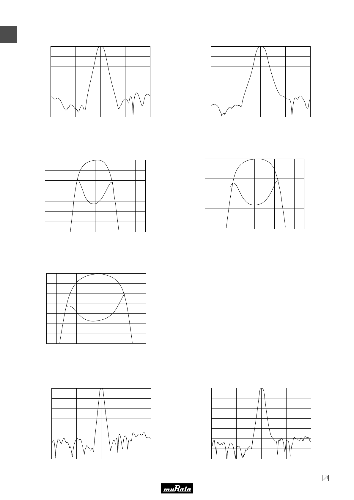
SFECV10M7KA00-R0
10.200 10.700
Frequency (MHz)
SFECV10M7HA00-R0
Frequency (MHz)
11.200 11.700
6.00
5.50
5.00
4.50
4.00
3.50
3.00
2.50
SFECV10M7JA00-R0
0
10
20
30
40
Attenuation (dB)
50
60
70
9.700
10.200 10.700
Frequency (MHz)
11.200 11.700
SFECV10M7GA00-R0
0 5.50
1 5.00
2 4.50
3 4.00
G.D.T. (µsec.)
4 3.50
Attenuation (dB)
5 3.00
6 2.50
7 2.00
10.500 10.600 10.700 10.800 10.900
Frequency (MHz)
G.D.T. (µsec.)
■ Frequency Characteristics
SFECV10M7FA00-R0
0 5.00
1 4.50
2 4.00
3 3.50
4 3.00
Attenuation (dB)
5 2.50
6 2.00
7 1.50
10.500 10.600 10.700 10.800 10.900
Frequency (MHz)
■ Frequency Characteristics (Spurious)
SFECV10M7KA00-R0
0
10
20
30
40
Attenuation (dB)
50
60
70
8.700
9.700 10.700
Frequency (MHz)
11.700 12.700
G.D.T. (µsec.)
SFECV10M7JA00-R0
0
10
20
30
40
Attenuation (dB)
50
60
70
8.700
9.700 10.700
Frequency (MHz)
11.700 12.700
Continued on the following page.
4
Page 6
Please read CAUTION and Notice in this catalog for safety. This catalog has only typical specifications. Therefore you are requested
to approve our product specification or to transact the approval sheet for product specification, before your ordering.
Continued from the preceding page.
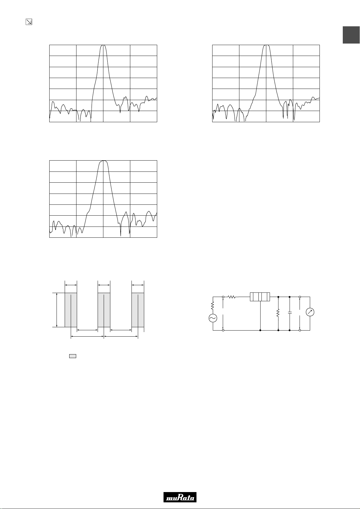
■ Frequency Characteristics (Spurious)
0
0
SFECV10M7HA00-R0
SFECV10M7GA00-R0
P61E7.pdf 01.10.17
1
10
20
30
40
Attenuation (dB)
50
60
70
8.700 10.7009.700 11.700 12.700
Frequency (MHz)
SFECV10M7FA00-R0
0
10
20
30
40
Attenuation (dB)
50
60
70
8.700 10.7009.700 11.700 12.700
Frequency (MHz)
10
20
30
40
Attenuation (dB)
50
60
70
8.700 10.7009.700 11.700 12.700
Frequency (MHz)
■ Standard Land Pattern Dimensions
1.2
4.0
Land
1.2 1.2
1.65
2.85 2.85
1.65
(in mm)
■ Test Circuit
Rg
S.S.G.
=-10dBm
E1
Rg = 50Ω R
C2 = 10 ± 2 pF (Including stray capacitance and Input capacitance
of RF Volt Meter)
E1 : S.S.G. S.S.G. Output Voltage
R
1
(1)
(2)
1 = 280Ω ±5% R2 = 330Ω ±5%
(1): Input
(2): Ground
(3): Output
(3)
C2
2
R
RF
E2
Voltmeter
5
Page 7
Please read CAUTION and Notice in this catalog for safety. This catalog has only typical specifications. Therefore you are requested
to approve our product specification or to transact the approval sheet for product specification, before your ordering.
P61E7.pdf 01.10.17
1
Chip CERAFILr SFECV Series Notice
■ Notice (Soldering and Mounting)
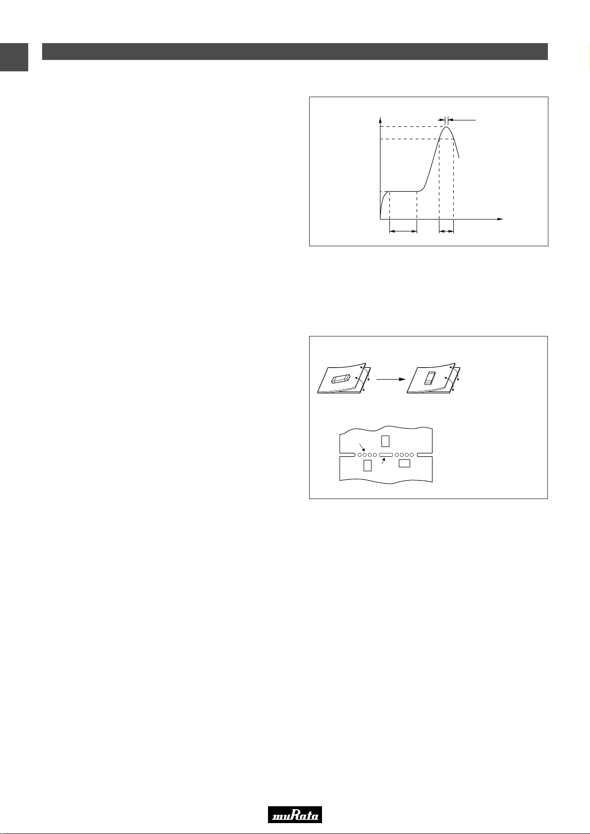
1. Standard Reflow Soldering Condition
(1) Reflow
240
230
150
Temperaturu(°C)
60 30
5sec.
Gradual Cooling
Time(sec.)
(2) Soldering Iron
Lead terminal is directly contacted with the tip of
soldering iron of 280±5˚C for 3.0±0.5 seconds.
2. Wash
The component cannot be withstand washing.
■ Notice (Handling)
1. The component will be damaged when an excessive
stress is applied.
2. The component may be damaged if excess mechanical
stress is applied to it mounted on the printed circuit
board.
3. Design layout of components on the PC board to
minimize the stress imposed on the warp or flexure of the
board.
4. After installing chips, if solder is excessively applied to
the circuit board, mechanical stress will cause
destruction resistance characteristics to lower. To
prevent this, be extremely careful in determining shape
and dimension before designing the circuit board
diagram.
5. When the positioning claws and pick up nozzle are worn,
the load is applied to the chip while positioning is
concentrated to one positioning accuracy, etc. Careful
checking and maintenance are necessary to prevent
unexpected trouble.
6. When correcting chips with a soldering iron, the tip of the
soldering iron should not directly touch the chip
component. Depending on the soldering conditions, the
effective area of terminations may be reduced. the use of
solder containing Ag should be done to prevent the
electrode erosion.
7. Do not clean or wash the component as it is not
hermetically sealed.
8. In case of covering filter with over coat, conditions such
as material of resin, cure temperature, and so on should
be evaluated well.
9. Do not use strong acidity flux, more than 0.2wt% chlorine
content, in re-flow soldering.
10. Accurate test circuit values are required to measure
electrical characteristics.It may be a cause of miscorrelation if there is any deviation, especially stray
capacitance, from the test circuit in the specification.
[Component direction]
[Component layout close to board]
Perforation
B
A
C
Slit
Put the
component
lateral to the
direction in
which stress
acts.
Susceptibility to
stress is in the order
of : A>C>B
6
Page 8
Please read CAUTION and Notice in this catalog for safety. This catalog has only typical specifications. Therefore you are requested
to approve our product specification or to transact the approval sheet for product specification, before your ordering.
Ceramic Filters (CERAFILr) for FM Receivers
CERAFILr Small Chip Type SFECS Series
P61E7.pdf 01.10.17
2
SFECS10M7 series for FM-receivers are small, high
performance and super thin (1.4mm) filters.
Piezoelectric element is connected in the sandwich
shape by ceramics substrate.
They have 1.4mm thickness and small mounting area.
(3.5x3.1mm)
New SFECS series and PFWCC(kHz filter for AM receiver)
enable customers to make AM/FM set so thin and small
sized.
■ Features
1. The filters are mountable by automatic placers.
2. They are slim, at only 1.4mm thickness, and have
a small mounting area (3.5x3.1mm) enabling
flexible PCB design.
3. Various bandwidths are available. Select a
suitable type in accordance with the desires
selectivity.
4. Operating temperature range :
-20 to +80 (degree C)
Storage temperature range :
-40 to +85 (degree C)
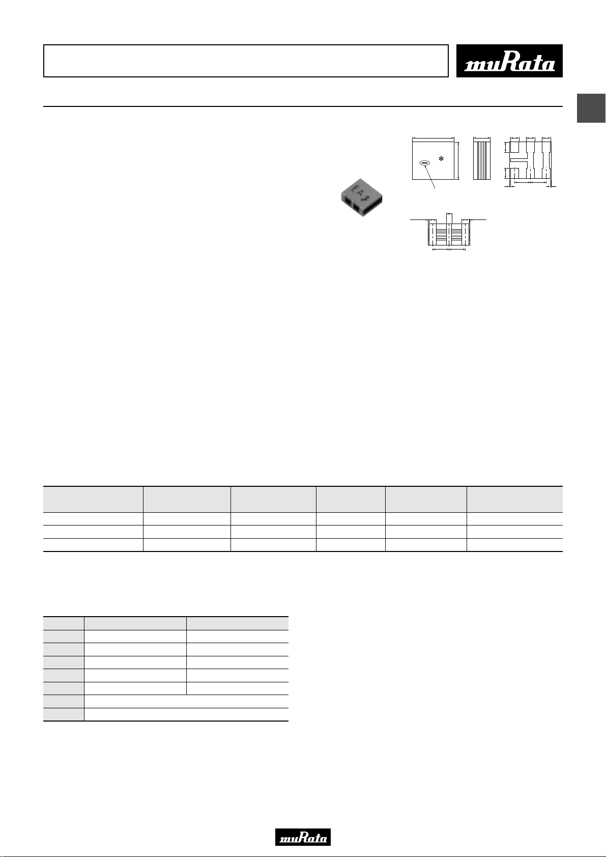
3.45T0.2
1.4T0.1
F A
3.10T0.2
Input electrode marker
W0.3
0.4
Y0.2
0.6T0.3 0.6T0.3
0-0.3 0-0.3
(1.35) (1.35)
0.7T0.3 0.7T0.3 0.7T0.3
(1)
(2) (3)
0.85T0.30.85T0.3
(4)
(1.30) (1.30)
0-0.3 0-0.3
(1) : Input
(2) : Ground
(3) : Float (Signal line)
(4) : Output
(*) : Reference
: EIAJ Monthly Code
(in mm)
■ Applications
1. Small, thin radios
2. Headphone stereos
Part Number
SFECS10M7HA00-R0 10.700 ±30kHz within180 ±40kHz 470 max. within4.5 ±2.0 dB 30 min.
SFECS10M7GA00-R0 10.700 ±30kHz within230 ±50kHz 510 max. within3.5 ±2.0 dB 30 min.
SFECS10M7FA00-R0 10.700 ±30kHz within280 ±50kHz 590 max. within3.0 ±2.0 dB 30 min.
Area of Attenuation : [within 20dB] Area of Spurious Attenuation : [within 9MHz to 12MHz]
Center frequency(fo) defined by the center of 3dB bandwidth.
Center Frequency (fo)
(MHz)
3dB Bandwidth
(kHz)
Attenuation
(kHz)
Insertion Loss
(dB)
Spurious Attenuation
■ Center Frequency Rank Code
CODE
D
B
A
C
E
Z
M
30kHz Step
10.64MHz±30kHz
10.67MHz±30kHz
10.70MHz±30kHz
10.73MHz±30kHz
10.76MHz±30kHz
Combination A,B,C,D,E
Combination A,B,C
25kHz Step
10.650MHz±25kHz
10.675MHz±25kHz
10.700MHz±25kHz
10.725MHz±25kHz
10.750MHz±25kHz
(dB)
7
Page 9
Please read CAUTION and Notice in this catalog for safety. This catalog has only typical specifications. Therefore you are requested
to approve our product specification or to transact the approval sheet for product specification, before your ordering.
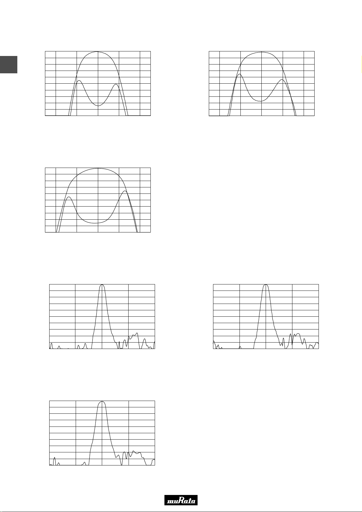
■ Frequency Characteristics
SFECS10M7HA00-R0
SFECS10M7GA00-R0
P61E7.pdf 01.10.17
0
2
2
4
6
Attenuation (dB)
8
10
10.500 10.600 10.700 10.800 10.900
Frequency (MHz)
5.60
5.40
5.20
5.00
4.80
4.60
4.40
4.20
4.00
3.80
3.60
G.D.T. (µsec.)
0
2
4
6
Attenuation (dB)
8
10
10.500 10.600 10.700 10.800 10.900
Frequency (MHz)
5.00
4.80
4.60
4.40
4.20
4.00
3.80
3.60
3.40
3.20
3.00
G.D.T. (µsec.)
SFECS10M7FA00-R0
0
2
4
6
Attenuation (dB)
8
10
10.500 10.600 10.700 10.800 10.900
Frequency (MHz)
4.60
4.40
4.20
4.00
3.80
3.60
3.40
3.20
3.00
2.80
2.60
G.D.T. (µsec.)
■ Frequency Characteristics (Spurious)
SFECS10M7HA00-R0
0
10
20
30
Attenuation (dB)
40
50
8.700 9.700 10.700 11.700 12.700
0
10
20
30
Attenuation (dB)
40
Frequency (MHz)
SFECS10M7FA00-R0
SFECS10M7GA00-R0
0
10
20
30
Attenuation (dB)
40
50
8.700 9.700 10.700 11.700 12.700
Frequency (MHz)
50
8.700 9.700 10.700 11.700 12.700
Frequency (MHz)
8
Page 10
Please read CAUTION and Notice in this catalog for safety. This catalog has only typical specifications. Therefore you are requested
to approve our product specification or to transact the approval sheet for product specification, before your ordering.
P61E7.pdf 01.10.17
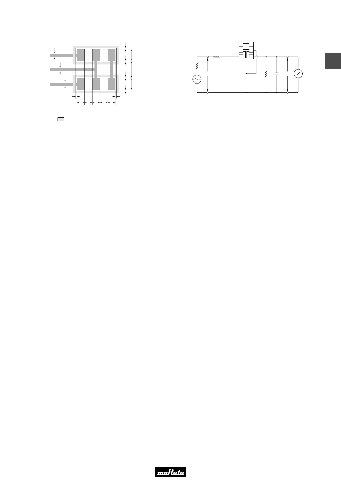
■ Standard Land Pattern Dimensions
0.3
0.3
0.3
(1) : Input (2) : Ground (3) : Float Signal Line (4) : Out put
It shows solder resist land pattern.
(4)
(1) (2) (3)
0.1
0.8 0.6 0.8 0.6 0.8
■ Test Circuit
0.10.10.10.1
1.051.401.05
Rg
S.S.G.
=-10dBm
0.1
(in mm)
R1
(3)
(2)
(4)(1)
Rg=50Ω
R1=280Ω
R2=330Ω
C2=10pF
(Including stray capacitance
and Input capacitance of RF Voltmeter)
E2C2E1 R2
RF
Voltmeter
(1) : Input
(2) : Ground
(3) : Float
(4) : Output
2
9
Page 11
Please read CAUTION and Notice in this catalog for safety. This catalog has only typical specifications. Therefore you are requested
to approve our product specification or to transact the approval sheet for product specification, before your ordering.
P61E7.pdf 01.10.17
Chip CERAFILr SFECS Series Notice
■ Notice (Soldering and Mounting)
2
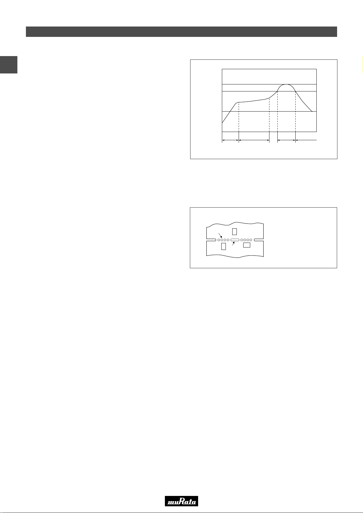
1. Standard Reflow Soldering Condition
(1) Reflow
Peak
240
200
Pre-heating
100
Temperature (˚C)
(120-170˚C)
(240˚C max.)
Heating
(200˚C)
Gradual
Cooling
(2) Soldering Iron
Filter shall be soldered at 280±5˚C for 3.0±0.5 seconds.
The soldering iron shall not touch the filter white soldering.
2. Wash
The component cannot be withstand washing.
■ Notice (Handling)
1. The component will be damaged when an excessive
stress is applied.
2. The component may be damaged if excess mechanical
stress is applied to it mounted on the printed circuit
board.
3. Design layout of components on the PC board to
minimize the stress imposed on the warp or flexure of the
board.
4. After installing chips, if solder is excessively applied to
the circuit board, mechanical stress will cause destruction
resistance characteristics to lower. To prevent this, be
extremly careful in determining shape and dimension
before designing the circuit board diagram.
5. When the positioning claws and pick up nozzle are worn,
the load is applied to the chip while positioning is
concentrated to one positioning accuracy, etc. Careful
checking and maintenance are necessary to prevent
unexpected trouble.
6. When correcting chips with a soldering iron, the tip of the
soldering iron should not directly touch the chip
component. Depending on the soldering conditions, the
effective area of terminations may be reduced. The use
of solder containing Ag should be done to prevent the
electrode erosion.
7. Do not clean or wash the component as it is not
hermetically sealed.
8. In case of covering filter with over coat, conditions such
as material of resin, cure temperature, and so on should
be evaluated well.
9. Do not use strong acidity flux, more than 0.2wt% chlorine
content, in re-flow soldering.
10. Accurate test circuit values are required to measure
electrical characteristics.
It may be a cause of mis-correlation if there is any
deviation, especially stray capacitance, from the test
circuit in the specification.
30 sec.
min.
60-120 sec.
[Component layout close to board]
Perforation
B
A
C
Slit
30 sec.
120 sec.
max.
min.
Susceptibility to
stress is in the order
of : A>C>B
10
Page 12
Please read CAUTION and Notice in this catalog for safety. This catalog has only typical specifications. Therefore you are requested
to approve our product specification or to transact the approval sheet for product specification, before your ordering.
Ceramic Filters (CERAFILr) for FM Receivers
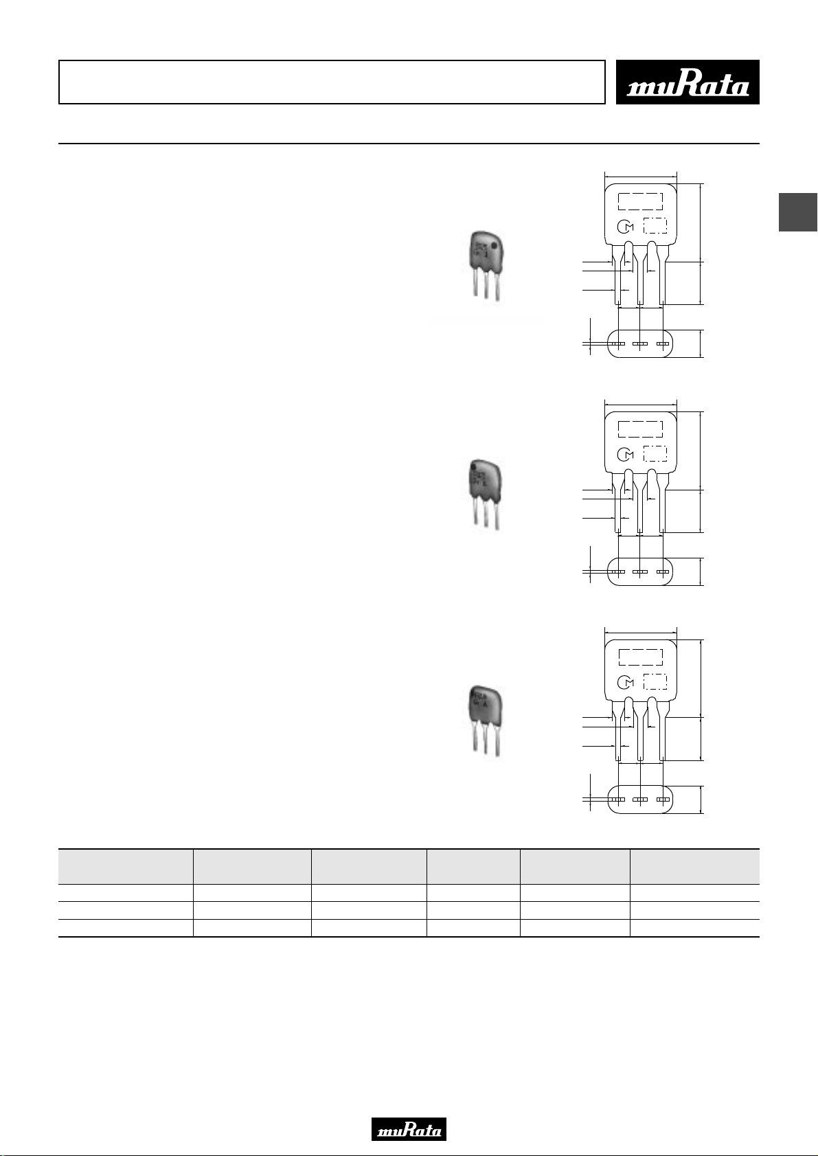
CERAFILr Standard Lead Type
SFELA10M7 series for FM-receivers are monolithic type
ceramic filters which use the energy trapped thickness
vibration-mode of the piezoelectric ceramic.
■ Features
1. These miniature filters have high mechanical
strength.
2. Low loss, favorable waveform symmetry, and high
selectivity.
3. Various band widths are available for applications
in wide to narrow bands.
4. Small dispersion and stable characteristics.
5. Change in center frequency is typically within
±30ppm/(degree C) at -20 to +80 (degree C).
6. High reliability.
SFELA10M7HA00-B0
SFELA10M7GA00-B0
1.38±0.2
1.7±0.1
0.5±0.1
0.3±0.1
1.38±0.2
1.7±0.1
0.5±0.1
0.3±0.1
7.0±2.0
M A R K I N G
2.5±0.2
(3)
7.0±2.0
M A R K I N G
2.5±0.2
(3)
P61E7.pdf 01.10.17
E I A J
(2)
(2)
C O D E
2.5±0.2
E I A J
C O D E
2.5±0.2
7.0±2.0
5.0±1.0
3.0±1.0
(1)
7.0±2.0
5.0±1.0
3.0±1.0
(1)
(1) : Input
(2) : Ground
(3) : Output
(in mm)
(1) : Input
(2) : Ground
(3) : Output
(in mm)
3
7.0±2.0
M A R K I N G
E I A J
Part Number
Center Frequency (fo)
(MHz)
3dB Bandwidth
(kHz)
SFELA10M7FA00-B0
Attenuation
(kHz)
1.38±0.2
1.7±0.1
0.5±0.1
0.3±0.1
Insertion Loss
(dB)
C O D E
2.5±0.2
2.5±0.2
(3)
(2)
Spurious Attenuation
7.0±2.0
5.0±1.0
3.0±1.0
(1)
(dB)
SFELA10M7HA00-B0 10.700 ±30kHz within180 ±40kHz 520 max. 7.0 max. 40 min.
SFELA10M7GA00-B0 10.700 ±30kHz within230 ±50kHz 570 max. within4.0 ±2.0dB 40 min.
SFELA10M7FA00-B0 10.700 ±30kHz within280 ±50kHz 650 max. within4.0 ±2.0dB 30 min.
Area of Attenuation : [within 20dB] Area of Spurious Attenuation : [within 9MHz to 12MHz]
Center frequency(fo) defined by the center of 3dB bandwidth.
(1) : Input
(2) : Ground
(3) : Output
(in mm)
11
Page 13
Please read CAUTION and Notice in this catalog for safety. This catalog has only typical specifications. Therefore you are requested
to approve our product specification or to transact the approval sheet for product specification, before your ordering.
P61E7.pdf 01.10.17
■ Center Frequency Rank Code
CODE
D
B
A
C
E
Z
3
M
30kHz Step
10.64MHz±30kHz
10.67MHz±30kHz
10.70MHz±30kHz
10.73MHz±30kHz
10.76MHz±30kHz
Combination A,B,C,D,E
Combination A,B,C
25kHz Step
10.650MHz±25kHz
10.675MHz±25kHz
10.700MHz±25kHz
10.725MHz±25kHz
10.750MHz±25kHz
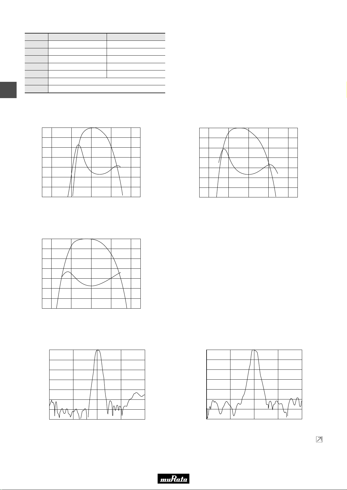
■ Frequency Characteristics
SFELA10M7HA00-B0
0
1
2
3
4
Attenuation (dB)
5
6
7
10.500 10.600 10.700 10.800 10.900
Frequency (MHz)
6.00
5.50
5.00
4.50
4.00
3.50
3.00
2.50
0
1
2
3
G.D.T. (µsec.)
4
Attenuation (dB)
5
6
7
10.500 10.600 10.700 10.800 10.900
SFELA10M7GA00-B0
Frequency (MHz)
5.50
5.00
4.50
4.00
3.50
3.00
2.50
2.00
G.D.T. (µsec.)
SFELA10M7FA00-B0
0
1
2
3
4
Attenuation (dB)
5
6
7
10.500 10.600 10.700 10.800 10.900
Frequency (MHz)
■ Frequency Characteristics (Spurious)
0
10
20
30
40
Attenuation (dB)
50
60
70
8.700 9.700 10.700 11.700 12.700
SFELA10M7HA00-B0
Frequency (MHz)
5.00
4.50
4.00
3.50
3.00
2.50
2.00
1.50
G.D.T. (µsec.)
SFELA10M7GA00-B0
0
10
20
30
40
Attenuation (dB)
50
60
70
8.700 9.700 10.700 11.700 12.700
Frequency (MHz)
12
Continued on the following page.
Page 14
Please read CAUTION and Notice in this catalog for safety. This catalog has only typical specifications. Therefore you are requested
to approve our product specification or to transact the approval sheet for product specification, before your ordering.
Continued from the preceding page.
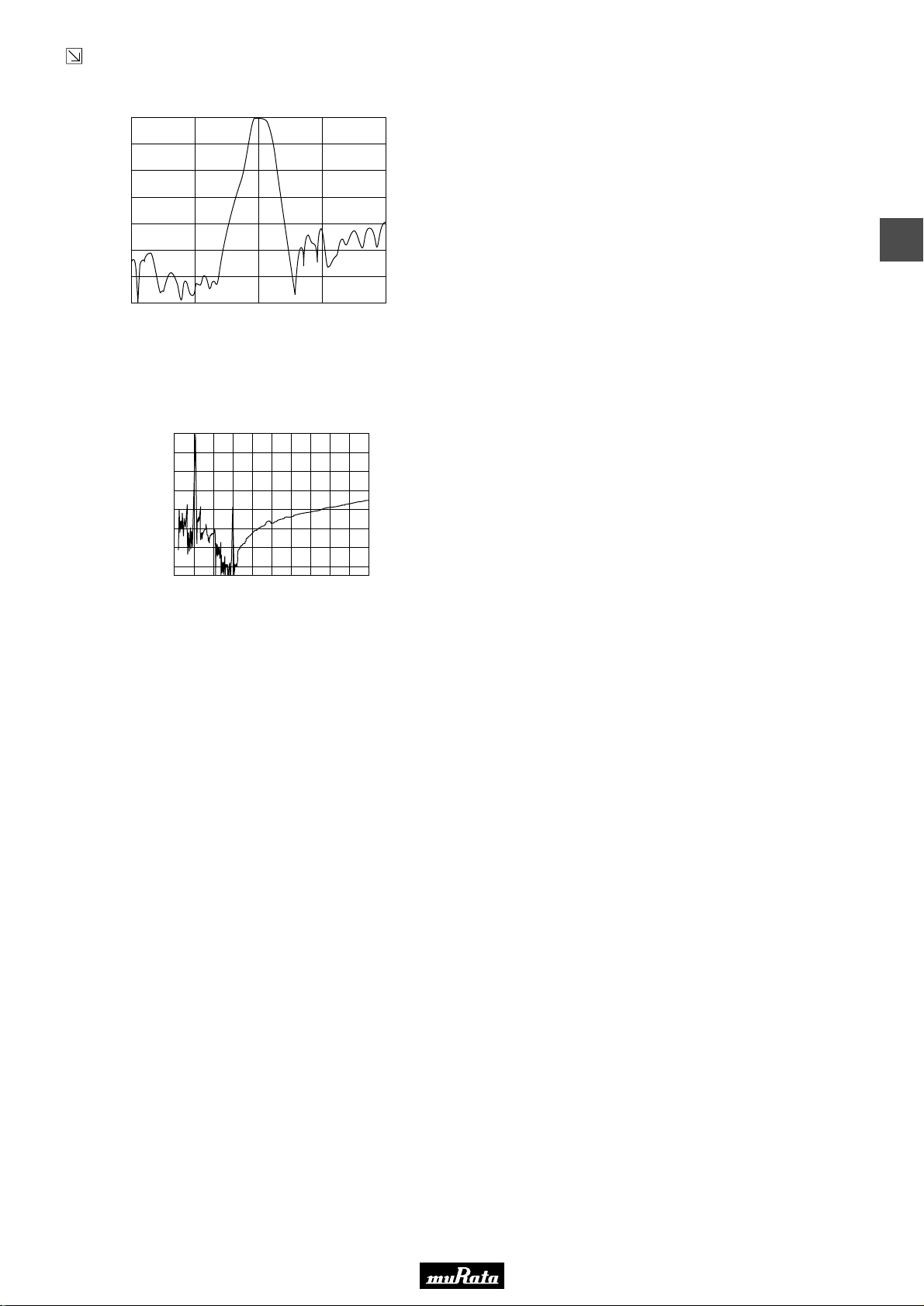
■ Frequency Characteristics (Spurious)
0
10
20
30
40
Attenuation (dB)
50
60
70
8.700 9.700 10.700 11.700 12.700
SFELA10M7FA00-B0
Frequency (MHz)
■ Spurious Response
SFELA10M7FA00-B0
0
10
20
30
40
50
Attenuation (dB)
60
70
0 20 40 60 80 100
Frequency (MHz)
P61E7.pdf 01.10.17
3
13
Page 15
Please read CAUTION and Notice in this catalog for safety. This catalog has only typical specifications. Therefore you are requested
to approve our product specification or to transact the approval sheet for product specification, before your ordering.
P61E7.pdf 01.10.17
Ceramic Filters (CERAFILr) for FM Receivers
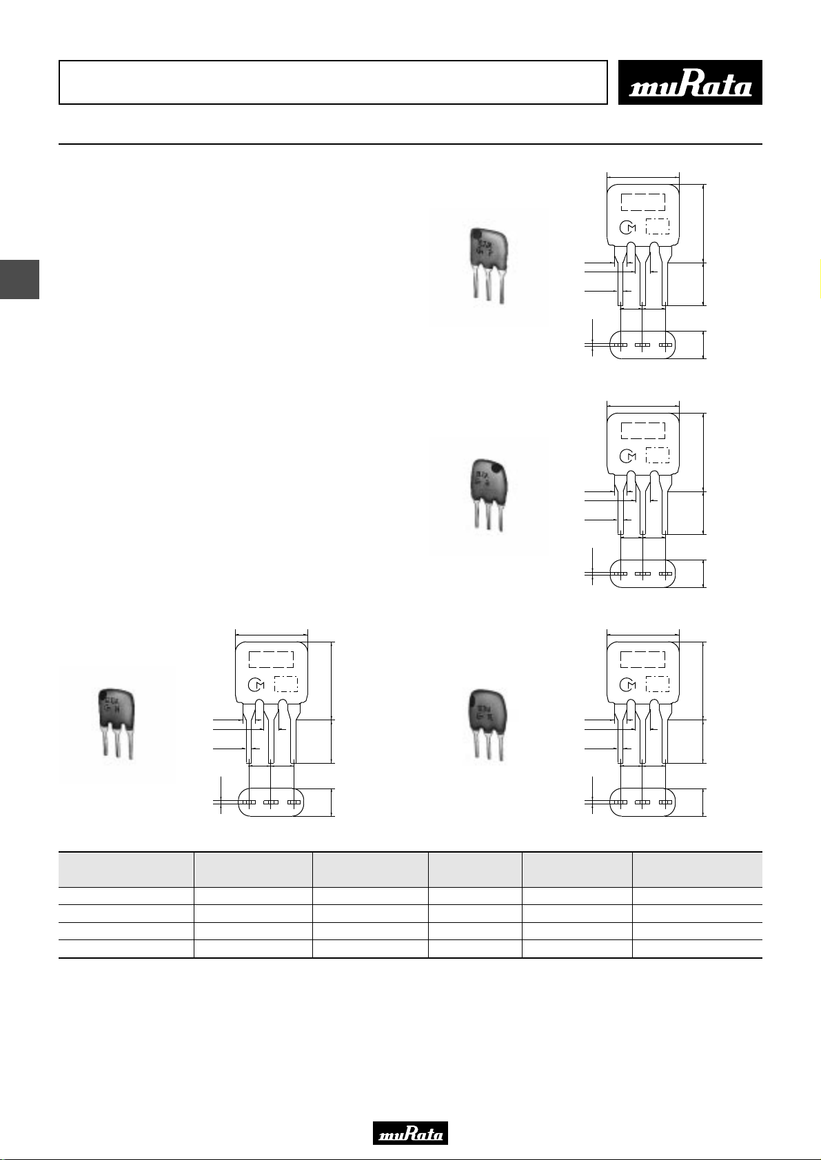
CERAFILr Low-loss Type
7.0±2.0
SFELA10M7 series for FM-receivers are monolithic type
ceramic filters which use the energy trapped thickness
vibration-mode of the piezoelectric ceramic.
■ Features
4
1. Insertion loss is 1 to 1.5dB lower than
conventional products. This types are useful for
elevating the sensitivity of sets.
2. Small dispersion and stable characteristics.
3. Excellent shape factor of frequency response.
4. Good waveform symmetry.
SFELA_JAA0-B0
1.38±0.2
1.7±0.1
0.5±0.1
0.3±0.1
M A R K I N G
2.5±0.2
(3)
7.0±2.0
(2)
E I A J
C O D E
2.5±0.2
7.0±2.0
5.0±1.0
(1) : Input
(2) : Ground
(3) : Output
3.0±1.0
(1)
(in mm)
SFELA_GAA0-B0
1.38±0.2
1.7±0.1
0.5±0.1
0.3±0.1
7.0±2.0
M A R K I N G
2.5±0.2
(3)
(2)
E I A J
C O D E
2.5±0.2
M A R K I N G
E I A J
C O D E
1.38±0.2
1.7±0.1
0.5±0.1
2.5±0.2
2.5±0.2
SFELA_HAA0-B0
7.0±2.0
5.0±1.0
(1) : Input
(2) : Ground
(3) : Output
3.0±1.0
(1)
(in mm)
SFELA_FAA0-B0
0.3±0.1
1.38±0.2
1.7±0.1
0.5±0.1
0.3±0.1
(3)
7.0±2.0
M A R K I N G
2.5±0.2
(3)
(2)
(2)
E I A J
C O D E
2.5±0.2
7.0±2.0
5.0±1.0
(1) : Input
(2) : Ground
(3) : Output
3.0±1.0
7.0±2.0
5.0±1.0
3.0±1.0
(in mm)
(1) : Input
(2) : Ground
(3) : Output
(in mm)
(1)
(1)
Part Number
Center Frequency (fo)
(MHz)
3dB Bandwidth
(kHz)
Attenuation
(kHz)
Insertion Loss
(dB)
Spurious Attenuation
SFELA10M7JAA0-B0 10.700 ±30kHz within150 ±40kHz 360 max. within4.5 ±2.0dB 35 min.
SFELA10M7HAA0-B0 10.700 ±30kHz within180 ±40kHz 470 max. within3.5 ±1.5dB 35 min.
SFELA10M7GAA0-B0 10.700 ±30kHz within230 ±50kHz 520 max. within3.0 ±2.0dB 35 min.
SFELA10M7FAA0-B0 10.700 ±30kHz within280 ±50kHz 590 max. within2.5 ±2.0dB 30 min.
Area of Attenuation : [within 20dB] Area of Spurious Attenuation : [within 9MHz to 12MHz]
Center frequency(fo) defined by the center of 3dB bandwidth.
14
(dB)
Page 16
Please read CAUTION and Notice in this catalog for safety. This catalog has only typical specifications. Therefore you are requested
to approve our product specification or to transact the approval sheet for product specification, before your ordering.
■ Center Frequency Rank Code
CODE
D
B
A
C
E
Z
M
30kHz Step
10.64MHz±30kHz
10.67MHz±30kHz
10.70MHz±30kHz
10.73MHz±30kHz
10.76MHz±30kHz
Combination A,B,C,D,E
Combination A,B,C
25kHz Step
10.650MHz±25kHz
10.675MHz±25kHz
10.700MHz±25kHz
10.725MHz±25kHz
10.750MHz±25kHz
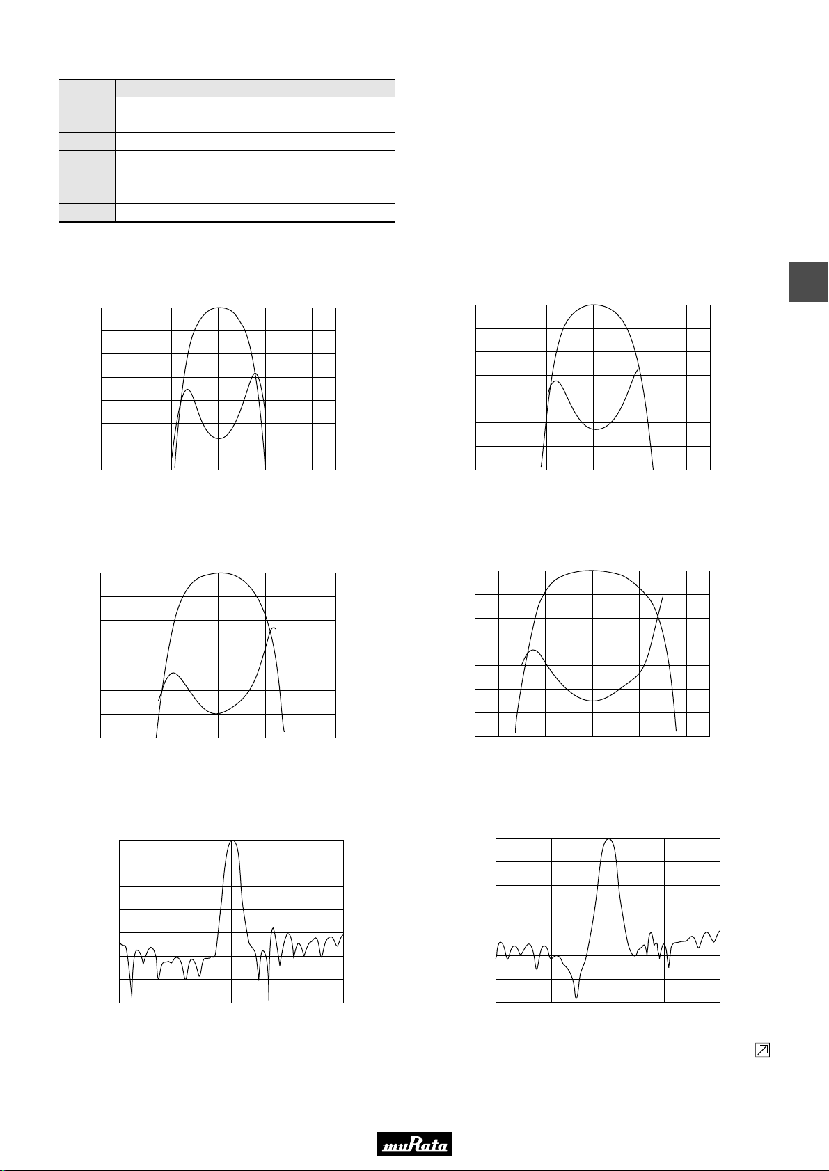
■ Frequency Characteristics
SFELA10M7JAA0-B0
0 7.50
1 7.00
2 6.50
3 6.00
4 5.50
Attenuation (dB)
5 5.00
6 4.50
7 4.00
10.500 10.600 10.700 10.800 10.900
Frequency (MHz)
0
1
2
3
G.D.T. (µsec.)
4
Attenuation (dB)
5
6
7
10.500 10.600 10.700 10.800 10.900
SFELA10M7HAA0-B0
Frequency (MHz)
P61E7.pdf 01.10.17
6.50
6.00
5.50
5.00
4.50
G.D.T. (µsec.)
4.00
3.50
3.00
4
SFELA10M7GAA0-B0
0
1 6.00
2 5.50
3 5.00
4 4.50
Attenuation (dB)
5 4.00
6 3.50
7 3.00
10.500 10.600 10.700 10.800 10.900
Frequency (MHz)
■ Frequency Characteristics (Spurious)
SFELA10M7JAA0-B0
0
10
20
30
40
Attenuation (dB)
50
60
70
8.700 9.700 10.700 11.700 12.700
Frequency (MHz)
6.50
SFELA10M7FAA0-B0
0 5.50
1 5.00
2 4.50
3 4.00
G.D.T. (µsec.)
4 3.50
Attenuation (dB)
5 3.00
6 2.50
7 2.00
10.60010.500 10.700 10.800 10.900
Frequency (MHz)
G.D.T. (µsec.)
SFELA10M7HAA0-B0
0
10
20
30
40
Attenuation (dB)
50
60
70
8.700 9.700 10.700 11.700 12.700
Frequency (MHz)
Continued on the following page.
15
Page 17
Please read CAUTION and Notice in this catalog for safety. This catalog has only typical specifications. Therefore you are requested
to approve our product specification or to transact the approval sheet for product specification, before your ordering.
P61E7.pdf 01.10.17
Continued from the preceding page.
■ Frequency Characteristics (Spurious)
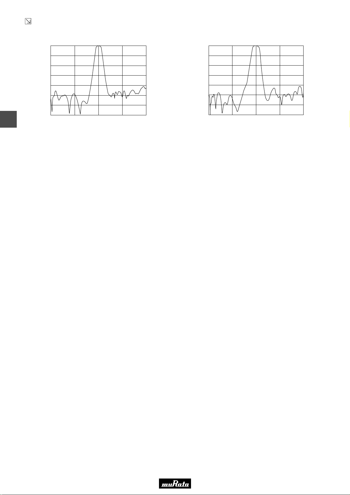
SFELA10M7GAA0-B0
0
10
20
30
40
Attenuation (dB)
50
60
70
4
8.700 9.700 10.700 11.700 12.700
Frequency (MHz)
0
10
20
30
40
Attenuation (dB)
50
60
70
8.700 9.700 10.700 11.700 12.700
SFELA10M7FAA0-B0
Frequency (MHz)
16
Page 18
Please read CAUTION and Notice in this catalog for safety. This catalog has only typical specifications. Therefore you are requested
to approve our product specification or to transact the approval sheet for product specification, before your ordering.
Ceramic Filters (CERAFILr) for FM Receivers
CERAFILr Low-profile Type
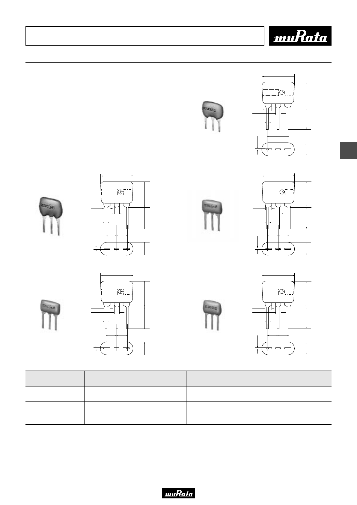
SFELB10M7 series for FM-receivers are monolithic type
ceramic filters which use the energy trapped thickness
vibration-mode of the piezoelectric ceramic.
■ Features
1. Installed height is 5 mm, making it well suited for
compact, thin sets.
2. Environmental reliability is the same as those of
the ceramic filter SFELA10M7 series.
SFELB10M7KA00-B0
1.5±0.1
1.3±0.1
0.5±0.1
0.3±0.1
7.5±2.0
M A R K I N G
2.5
±
0.2
2.5±0.2
(1) (2) (3)
P61E7.pdf 01.10.17
E I A J
C O D E
6.0 max.
5.0±1.0
(1) : Input
(2) : Ground
(3) : Output
3.0±1.0
in mm
5
SFELB10M7JA00-B0
SFELB10M7GA00-B0
1.5±0.1
1.3±0.1
0.5±0.1
0.3±0.1
1.5±0.1
1.3±0.1
0.5±0.1
0.3±0.1
7.5±2.0
M A R K I N G
2.5
±
0.2
2.5±0.2
(1) (2) (3)
7.5±2.0
M A R K I N G
2.5
±
0.2
2.5±0.2
(1) (2) (3)
E I A J
C O D E
E I A J
C O D E
6.0 max.
5.0±1.0
3.0±1.0
6.0 max.
5.0±1.0
3.0±1.0
(1) : Input
(2) : Ground
(3) : Output
in mm
(1) : Input
(2) : Ground
(3) : Output
in mm
SFELB10M7HA00-B0
SFELB10M7FA00-B0
1.5±0.1
1.3±0.1
0.5±0.1
0.3±0.1
1.5±0.1
1.3±0.1
0.5±0.1
0.3±0.1
7.5±2.0
M A R K I N G
2.5
±
0.2
2.5±0.2
(1) (2) (3)
7.5±2.0
M A R K I N G
2.5
±
0.2
2.5±0.2
(1) (2) (3)
E I A J
C O D E
E I A J
C O D E
6.0 max.
5.0±1.0
3.0±1.0
6.0 max.
5.0±1.0
3.0±1.0
(1) : Input
(2) : Ground
(3) : Output
in mm
(1) : Input
(2) : Ground
(3) : Output
in mm
Part Number
Center Frequency (fo)
(MHz)
3dB Bandwidth
(kHz)
Attenuation
(kHz)
Insertion Loss
(dB)
Spurious Attenuation
(dB)
SFELB10M7KA00-B0 10.700 ±30kHz within110 ±30kHz 350 max. within7.0 ±2.0dB 30 min.
SFELB10M7JA00-B0 10.700 ±30kHz within150 ±40kHz 360 max. within4.5 ±2.0dB 35 min.
SFELB10M7HA00-B0 10.700 ±30kHz within180 ±40kHz 470 max. within3.5 ±2.0dB 35 min.
SFELB10M7GA00-B0 10.700 ±30kHz within230 ±50kHz 570 max. within3.0 ±2.0dB 40 min.
SFELB10M7FA00-B0 10.700 ±30kHz within280 ±50kHz 650 max. within3.0 ±2.0dB 30 min.
Area of Attenuation : [within 20dB] Area of Spurious Attenuation : [within 9MHz to 12MHz]
Center frequency(fo) defined by the center of 3dB bandwidth.
17
Page 19
Please read CAUTION and Notice in this catalog for safety. This catalog has only typical specifications. Therefore you are requested
to approve our product specification or to transact the approval sheet for product specification, before your ordering.
P61E7.pdf 01.10.17
■ Center Frequency Rank Code
CODE
D
B
A
C
E
Z
M
30kHz Step
10.64MHz±30kHz
10.67MHz±30kHz
10.70MHz±30kHz
10.73MHz±30kHz
10.76MHz±30kHz
Combination A,B,C,D,E
Combination A,B,C
25kHz Step
10.650MHz±25kHz
10.675MHz±25kHz
10.700MHz±25kHz
10.725MHz±25kHz
10.750MHz±25kHz
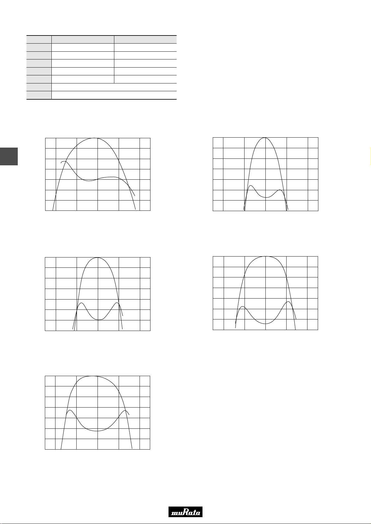
■ Frequency Characteristics
SFELB10M7KA00-B0
0 8.00
1 7.50
5
2 7.00
3 6.50
4 6.00
Attenuation (dB)
5 5.50
6 5.00
7 4.50
10.620 10.660 10.700 10.740 10.780
Frequency (MHz)
G.D.T. (µsec.)
0 7.50
1
2 6.50
3 6.00
4 5.50
Attenuation (dB)
5 5.00
6 4.50
7 4.00
SFELB10M7JA00-B0
10.60010.500 10.800 10.900
10.700
Frequency (MHz)
7.00
G.D.T. (µsec.)
SFELB10M7HA00-B0
0
1 6.50
2 6.00
3 5.50
4 5.00
Attenuation (dB)
5 4.50
6 4.00
7 3.50
10.70010.60010.500 10.800 10.900
Frequency (MHz)
SFELB10M7FA00-B0
0
1 5.00
2 4.50
3 4.00
4 3.50
Attenuation (dB)
5 3.00
6 2.50
7 2.00
10.700 10.800 10.90010.60010.500
Frequency (MHz)
7.00
5.50
SFELB10M7GA00-B0
0 6.50
1 6.00
2 5.50
3 5.00
G.D.T. (µsec.)
G.D.T. (µsec.)
4 4.50
Attenuation (dB)
5 4.00
6 3.50
7 3.00
10.500 10.600 10.700 10.800 10.900
Frequency (MHz)
G.D.T. (µsec.)
18
Page 20
Please read CAUTION and Notice in this catalog for safety. This catalog has only typical specifications. Therefore you are requested
to approve our product specification or to transact the approval sheet for product specification, before your ordering.
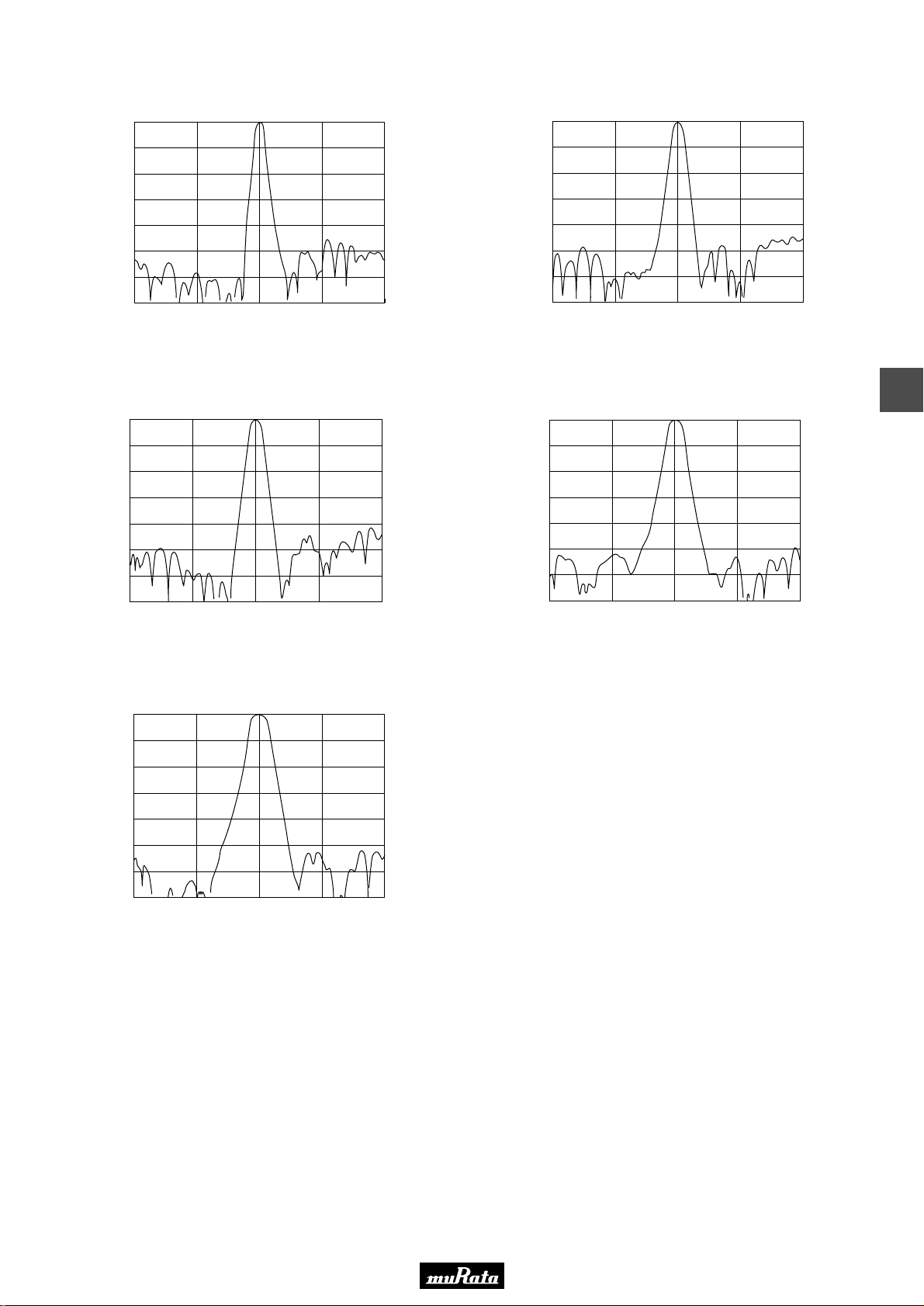
■ Frequency Characteristics (Spurious)
SFELB10M7KA00-B0
0
10
20
30
40
Attenuation (dB)
50
60
70
8.700 9.700 10.700 11.700 12.700
Frequency (MHz)
0
10
20
30
40
Attenuation (dB)
50
60
70
SFELB10M7JA00-B0
9.7008.700 11.700 12.700
10.700
Frequency (MHz)
P61E7.pdf 01.10.17
SFELB10M7HA00-B0
0
10
20
30
40
Attenuation (dB)
50
60
70
9.7008.700 11.700 12.700
10.700
Frequency (MHz)
0
10
20
30
40
Attenuation (dB)
50
60
70
8.700 9.700 10.700 11.700 12.700
SFELB10M7GA00-B0
Frequency (MHz)
5
SFELB10M7FA00-B0
0
10
20
30
40
Attenuation (dB)
50
60
70
10.700 11.700 12.7009.7008.700
Frequency (MHz)
19
Page 21
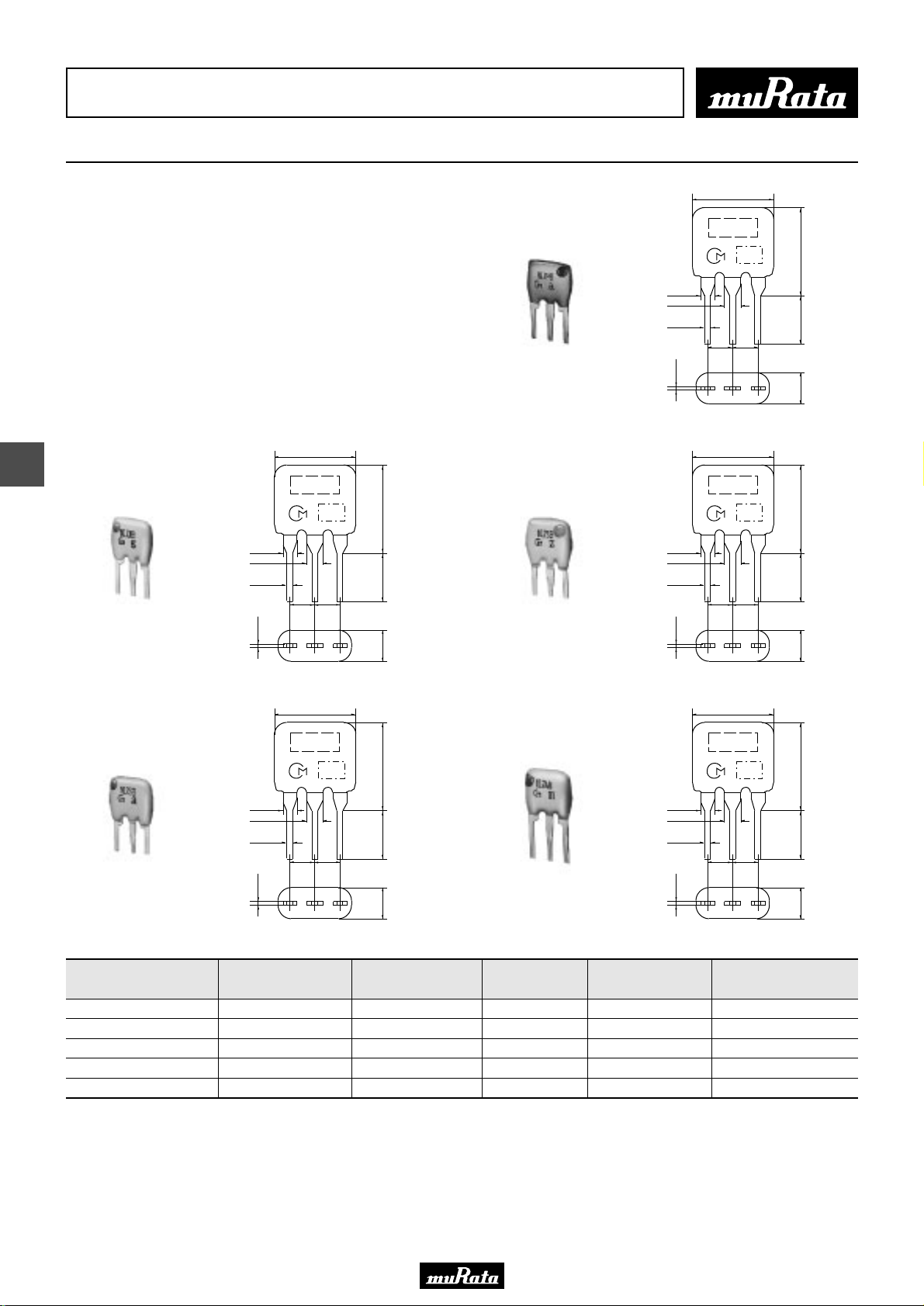
Please read CAUTION and Notice in this catalog for safety. This catalog has only typical specifications. Therefore you are requested
to approve our product specification or to transact the approval sheet for product specification, before your ordering.
Ceramic Filters (CERAFILr) for FM Receivers
CERAFILr Lower Spurious Response Type
SFELA10M7 series for FM-receivers are monolithic type
ceramic filters which use the energy trapped thickness
vibration-mode of the piezoelectric ceramic.
■ Features
1. This type has lower spurious response compared to
the standard filters.
2. This types are suitable for higher spurious
suppression radio.
SFELA10M7KAB0-B0
1.38±0.2
1.7±0.1
0.5±0.1
0.3±0.1
P61E7.pdf 01.10.17
7.5±2.0
MARKING
EIAJ
CODE
2.5±0.2
2.5±0.2
7.0±2.0
5.0±1.03.0±1.0
(2)
7.5±2.0
(1)
(3)
7.5±2.0
6
SFELA10M7JAB0-B0
1.38±0.2
1.7±0.1
0.5±0.1
0.3±0.1
1.38±0.2
1.7±0.1
0.5±0.1
2.5±0.2
(3)
2.5±0.2
MARKING
EIAJ
CODE
2.5±0.2
(2)
7.5±2.0
MARKING
EIAJ
CODE
2.5±0.2
7.0±2.0
1.38±0.2
1.7±0.1
5.0±1.03.0±1.0
SFELA10M7HAB0-B0
(1)
7.0±2.0
1.38±0.2
1.7±0.1
5.0±1.03.0±1.0
0.5±0.1
0.3±0.1
0.5±0.1
2.5±0.2
(3)
2.5±0.2
MARKING
EIAJ
CODE
2.5±0.2
(2)
7.5±2.0
MARKING
EIAJ
CODE
2.5±0.2
7.0±2.0
5.0±1.03.0±1.0
(1)
7.0±2.0
5.0±1.03.0±1.0
SFELA10M7GAB0-B0
Part Number
0.3±0.1
(3)
(2)
Center Frequency (fo)
(MHz)
(1)
3dB Bandwidth
(kHz)
SFELA10M7FAB0-B0
Attenuation
(kHz)
0.3±0.1
Insertion Loss
(dB)
(3)
(1)
(2)
Spurious Attenuation
SFELA10M7KAB0-B0 10.700 ±30kHz within110 ±30kHz 350 max. 7.0 ±2.0dB 45 min.
SFELA10M7JAB0-B0 10.700 ±30kHz within150 ±40kHz 380 max. 5.5 ±2.0dB 45 min.
SFELA10M7HAB0-B0 10.700 ±30kHz within180 ±40kHz 520 max. 5.0 ±2.0dB 45 min.
SFELA10M7GAB0-B0 10.700 ±30kHz within230 ±50kHz 570 max. 3.0 ±2.0dB 45 min.
SFELA10M7FAB0-B0 10.700 ±30kHz within280 ±50kHz 650 max. 3.0 ±2.0dB 45 min.
Area of Attenuation : [within 20dB] Area of Spurious Attenuation : [within 9MHz to 12MHz]
Center frequency(fo) defined by the center of 3dB bandwidth.
20
(dB)
Page 22
Please read CAUTION and Notice in this catalog for safety. This catalog has only typical specifications. Therefore you are requested
to approve our product specification or to transact the approval sheet for product specification, before your ordering.
■ Center Frequency Rank Code
CODE
D
B
A
C
E
Z
M
30kHz Step
10.64MHz±30kHz
10.67MHz±30kHz
10.70MHz±30kHz
10.73MHz±30kHz
10.76MHz±30kHz
Combination A,B,C,D,E
Combination A,B,C
25kHz Step
10.650MHz±25kHz
10.675MHz±25kHz
10.700MHz±25kHz
10.725MHz±25kHz
10.750MHz±25kHz
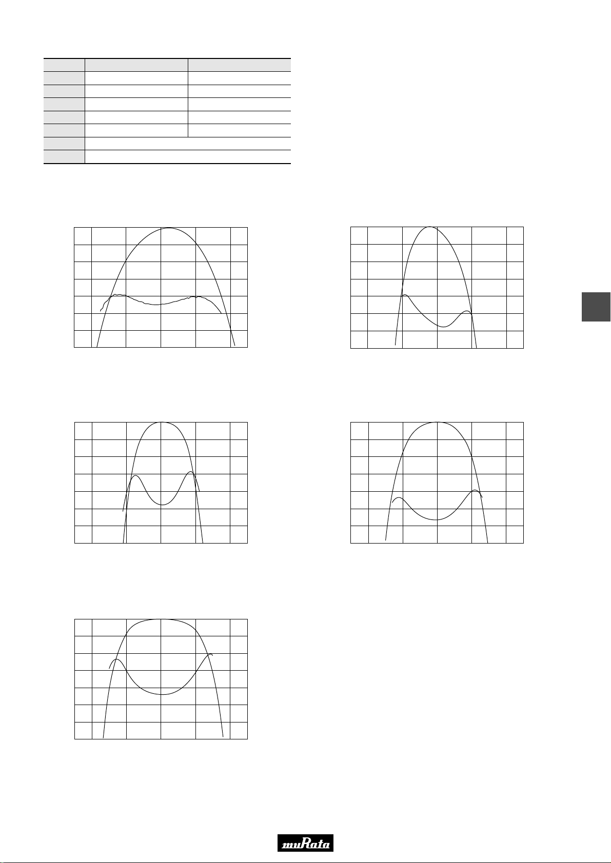
■ Frequency Characteristics
SFELA10M7KAB0-B0
0
1 7.50
2 7.00
3 6.50
4 6.00
Attenuation (dB)
5 5.50
6 5.00
7 4.50
10.700 10.740 10.78010.66010.620
Frequency (MHz)
8.00
0
1 6.50
2
3
G.D.T. (µsec.)
4 5.00
Attenuation (dB)
5 4.50
6 4.00
7 3.50
SFELA10M7JAB0-B0
Frequency (MHz)
P61E7.pdf 01.10.17
7.00
6.00
5.50
G.D.T. (µsec.)
6
10.700 10.800 10.90010.60010.500
SFELA10M7HAB0-B0
0 6.50
1 6.00
2 5.50
3 5.00
4 4.50
Attenuation (dB)
5 4.00
6 3.50
7 3.00
10.500 10.600 10.700 10.800 10.900
Frequency (MHz)
SFELA10M7FAB0-B0
0 5.00
1 4.50
2 4.00
3 3.50
4 3.00
Attenuation (dB)
5 2.50
6 2.00
7 1.50
10.500 10.600 10.700 10.800 10.900
Frequency (MHz)
SFELA10M7GAB0-B0
0 6.00
1 5.50
2 5.00
3 4.50
G.D.T. (µsec.)
G.D.T. (µsec.)
4 4.00
Attenuation (dB)
5 3.50
6 3.00
7 2.50
10.500 10.600 10.700 10.800 10.900
Frequency (MHz)
G.D.T. (µsec.)
21
Page 23
Please read CAUTION and Notice in this catalog for safety. This catalog has only typical specifications. Therefore you are requested
to approve our product specification or to transact the approval sheet for product specification, before your ordering.
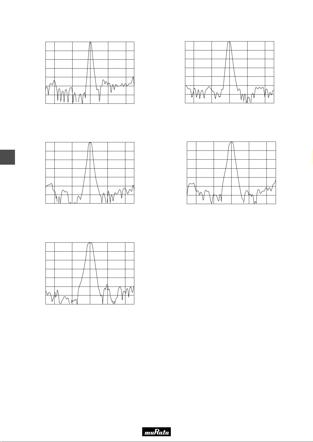
■ Frequency Characteristics (Spurious)
SFELA10M7KAB0-B0
0
10
20
30
40
Attenuation (dB)
50
60
70
10.700 11.700 12.7008.700 9.700
Frequency (MHz)
0
10
20
30
40
Attenuation (dB)
50
60
70
SFELA10M7JAB0-B0
10.700 11.700 12.7008.700 9.700
Frequency (MHz)
P61E7.pdf 01.10.17
SFELA10M7HAB0-B0
0
10
6
20
30
40
Attenuation (dB)
50
60
70
8.700 9.700 10.700 11.700 12.700
Frequency (MHz)
0
10
20
30
40
Attenuation (dB)
50
60
70
SFELA10M7GAB0-B0
8.700 9.700 10.700 11.700 12.700
Frequency (MHz)
SFELA10M7FAB0-B0
0
10
20
30
40
Attenuation (dB)
50
60
70
8.700 9.700 10.700 11.700 12.700
Frequency (MHz)
22
Page 24
Please read CAUTION and Notice in this catalog for safety. This catalog has only typical specifications. Therefore you are requested
to approve our product specification or to transact the approval sheet for product specification, before your ordering.
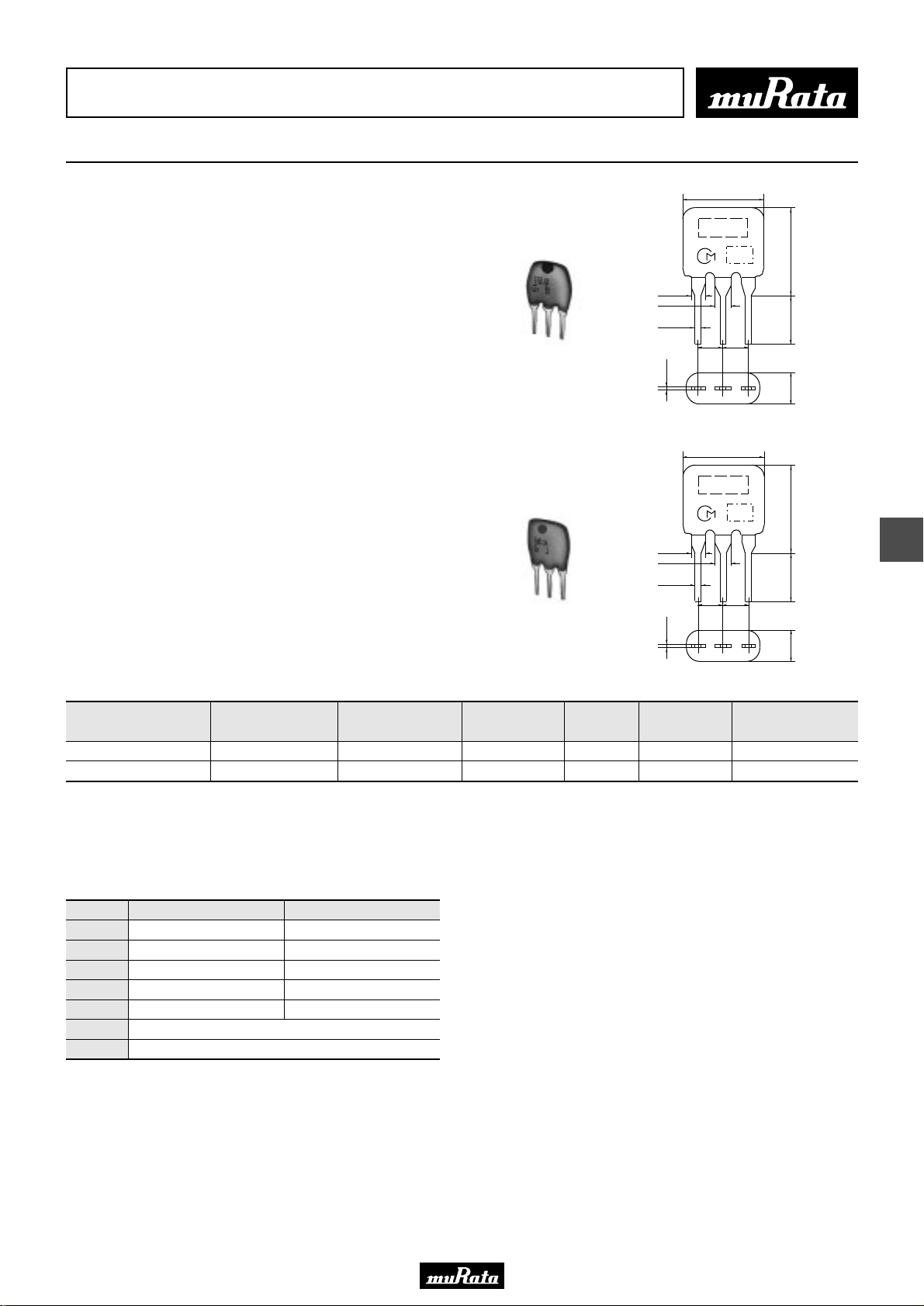
Ceramic Filters (CERAFILr) for FM Receivers
CERAFILr Wider Band-width Type
SFELA10M7 Series for FM-receivers are monolithic type
ceramic filters which use the energy trapped thickness
vibration-mode of the piezoelectric ceramic.
■ Features
1. Realizes wider or narrower band characteristics not
obtained by conventional ceramic filters.
2. Temperature characteristics are the best available,
the same as those of Murata's conventional ceramic
filters. Thus, even in the case of narrow band
filters, the center frequency is stable even if
temperature changes.
SFELA10M7EA00-B0
1.38±0.2
1.7±0.1
0.5±0.1
0.3±0.1
7.0±2.0
M A R K I N G
2.5±0.2
(3)
7.0±2.0
P61E7.pdf 01.10.17
E I A J
C O D E
2.5±0.2
(2)
7.0±2.0
5.0±1.0
3.0±1.0
(1)
(1) : Input
(2) : Ground
(3) : Output
(in mm)
M A R K I N G
E I A J
C O D E
1.38±0.2
1.7±0.1
0.5±0.1
2.5±0.2
2.5±0.2
Part Number
Center Frequency (fo)
(MHz)
Nominal
Center Frequency(fn)
(MHz)
SFELA10M7DF00-B0
3dB Bandwidth
(kHz)
Attenuation
(kHz)
0.3±0.1
(3)
Insertion Loss
(dB)
(1)
(2)
Spurious Attenuation
SFELA10M7EA00-B0 10.700 ±30kHz - within330 ±50kHz 680 max. within4.0 ±2.0dB 30 min.
SFELA10M7DF00-B0 - 10.700 fn±175 min. 950 max. within3.0 ±2.0dB 20 min.
Area of Attenuation : [within 20dB] Area of Spurious Attenuation : [within 9MHz to 12MHz]
Center frequency(fo) defined by the center of 3dB bandwidth.
(fn) means nominal center frequency.
■ Center Frequency Rank Code
CODE
D
B
A
C
E
Z
M
30kHz Step
10.64MHz±30kHz
10.67MHz±30kHz
10.70MHz±30kHz
10.73MHz±30kHz
10.76MHz±30kHz
Combination A,B,C,D,E
Combination A,B,C
25kHz Step
10.650MHz±25kHz
10.675MHz±25kHz
10.700MHz±25kHz
10.725MHz±25kHz
10.750MHz±25kHz
7.0±2.0
5.0±1.0
3.0±1.0
(dB)
(1) : Input
(2) : Ground
(3) : Output
(in mm)
7
23
Page 25
Please read CAUTION and Notice in this catalog for safety. This catalog has only typical specifications. Therefore you are requested
to approve our product specification or to transact the approval sheet for product specification, before your ordering.
P61E7.pdf 01.10.17
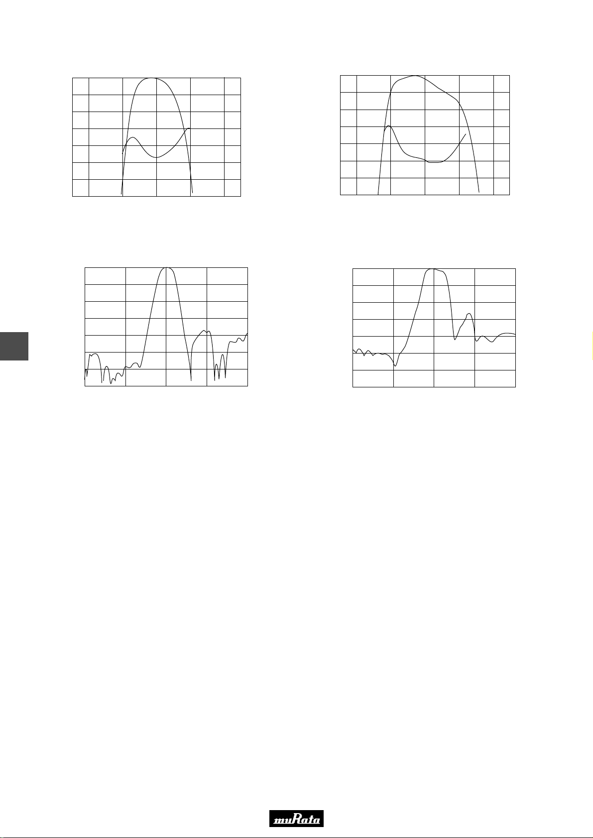
■ Frequency Characteristics
SFELA10M7EA00-B0
0
1
2
3
4
Attenuation (dB)
5
6
7
10.300 10.500 10.700 10.900 11.100
Frequency (MHz)
4.50
4.00
3.50
3.00
2.50
2.00
1.50
1.00
0
1
2
3
G.D.T. (µsec.)
4
Attenuation (dB)
5
6
7
10.300 10.500 10.700 10.900 11.100
SFELA10M7DF00-B0
Frequency (MHz)
4.00
3.50
3.00
2.50
2.00
1.50
1.00
0.50
G.D.T. (µsec.)
■ Frequency Characteristics (Spurious)
SFELA10M7EA00-B0
0
10
20
30
40
7
Attenuation (dB)
50
60
70
8.700 9.700 10.700 11.700 12.700
Frequency (MHz)
0
10
20
30
40
Attenuation (dB)
50
60
70
8.700 9.700 10.700 11.700 12.700
SFELA10M7DF00-B0
Frequency (MHz)
24
Page 26
Please read CAUTION and Notice in this catalog for safety. This catalog has only typical specifications. Therefore you are requested
to approve our product specification or to transact the approval sheet for product specification, before your ordering.
Ceramic Filters (CERAFILr) for FM Receivers
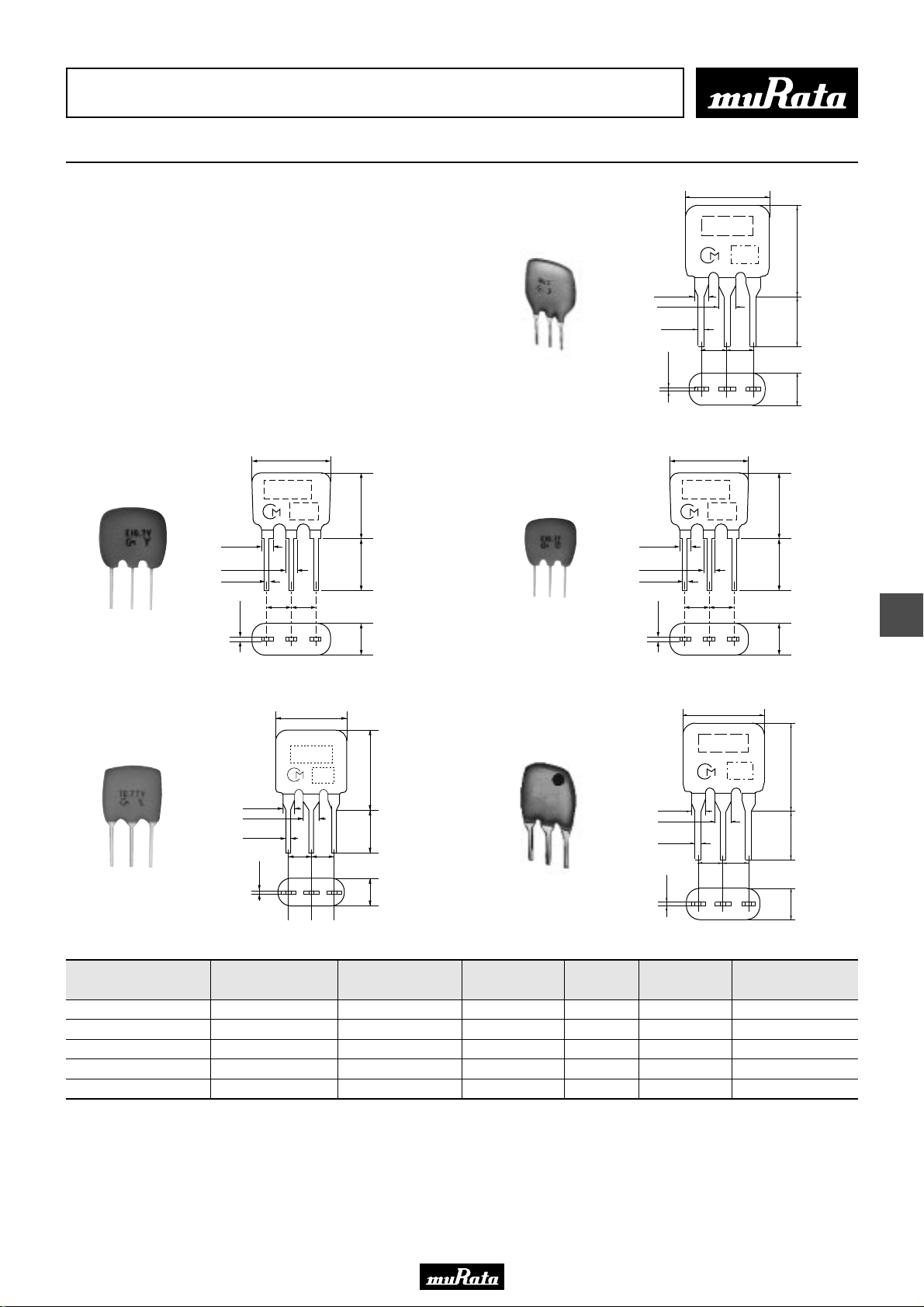
CERAFILr Narrow Band Type
P61E7.pdf 01.10.17
10.0±2.0
SFELA10M7LFTA/KAH0, SFVLA/SFKLA series realizes
narrower band characteristics not obtained by
conventional ceramic filters. Besides, low spurious
and temperature characteristics is stable. This series
suits for European car-audio or AM up conversion use
that needs narrow band characteristics.
7.0±2.0
MARKING
EIAJ
SFVLA10M7MF00-B0
1.65±0.1
1.4±0.1
0.5±0.1
0.3±0.1
CODE
2.5±0.2
2.5±0.2
(3) (2) (1)
7.0±2.05.0±1.03.0±1.0
(1) : Input
(2) : Ground
(3) : Output
in mm
SFKLA10M7NF00-B0
SFVLA10M7LF00-B0
1.38±0.2
1.7±0.1
1.65±0.1
1.4±0.1
0.5±0.1
0.3±0.1
0.5±0.1
0.3±0.1
MARKING
2.5±0.2
(3) (2) (1)
M A R K I N G
2.5±0.2
(3)
7.0±2.0
EIAJ
CODE
2.5±0.2
2.5±0.2
(2)
E I A J
C O D E
10.0±2.0
5.0±1.0
–1.0
+1.5
3.5
7.0±2.05.0±1.03.0±1.0
in mm
(1) : Input
(2) : Ground
(3) : Output
in mm
8
(1)
(dB)
7.0±2.0
M A R K I N G
E I A J
C O D E
2.5±0.2
2.5±0.2
(3)
(1)
(2)
Spurious Attenuation
7.0±2.0
5.0±1.0
3.0±1.0
(dB)
SFELA10M7LFTA01-B0
Part Number
7.0± 2.0
MARKING
EIAJ
CODE
1.38± 0.2
1.7± 0.1
0.5± 0.1
2.5
2.5
±0.2
±0.2
0.3± 0.1
(3) (2) (1)
Center Frequency (fo)
(MHz)
7.0± 2.0
5.0±1.0
(in mm)
(1) Input
3.0± 1.0
(2) Ground
(3) Output
Nominal
Center Frequency(fn)
(MHz)
SFELA10M7KAH0-B0
3dB Bandwidth
(kHz)
Attenuation
(kHz)
1.38±0.2
1.7±0.1
0.5±0.1
0.3±0.1
Insertion Loss
SFKLA10M7NF00-B0 10.700 ±15kHz - 20 min. 95 max. 6.0 max. 24 min.
SFVLA10M7MF00-B0 - 10.700 fn±13 min. 135 max. within5.5 ±2.5dB 30 min.
SFVLA10M7LF00-B0 - 10.700 fn±25 min. 200 max. within5.5 ±2.5dB 30 min.
SFELA10M7LFTA-B0 - 10.700 fn±25 min. 280 max. within7.0 ±2.0dB 30 min.
SFELA10M7KAH0-B0 10.700 ±30kHz - within110 ±30kHz 350 max. within7.0 ±2.0dB 30 min.
Area of Attenuation : [within 20dB] Area of Spurious Attenuation : [within 9MHz to 12MHz]
(1) : Input
(2) : Ground
(3) : Output
(in mm)
25
Page 27
Please read CAUTION and Notice in this catalog for safety. This catalog has only typical specifications. Therefore you are requested
to approve our product specification or to transact the approval sheet for product specification, before your ordering.
■ Center Frequency Rank Code
CODE
D
B
A
C
E
Z
M
30kHz Step
10.64MHz±30kHz
10.67MHz±30kHz
10.70MHz±30kHz
10.73MHz±30kHz
10.76MHz±30kHz
Combination A,B,C,D,E
Combination A,B,C
25kHz Step
10.650MHz±25kHz
10.675MHz±25kHz
10.700MHz±25kHz
10.725MHz±25kHz
10.750MHz±25kHz
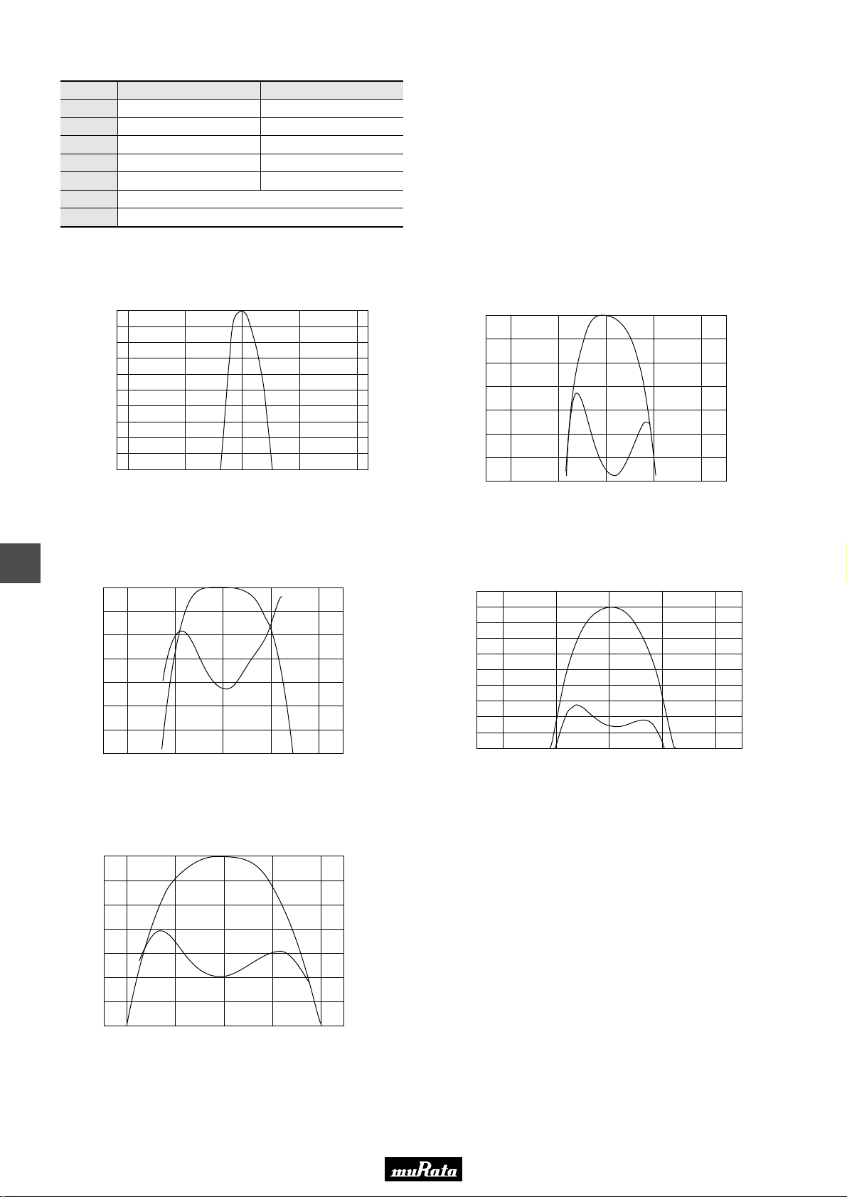
■ Frequency Characteristics
SFKLA10M7NF00-B0
0
0 19.0
1 18.0
2 17.0
3 16.0
SFVLA10M7MF00-B0
P61E7.pdf 01.10.17
Attenuation ( dB )
10
10.600
8
0 13.0
1 12.0
2 11.0
3 10.0
4 9.00
Attenuation (dB)
5 8.00
6 7.00
7 6.00
10.620 10.660 10.700 10.740 10.780
10.650 10.700
Frequency ( kHz )
SFVLA10M7LF00-B0
Frequency (MHz)
10.750
10.800
G.D.T. (µsec.)
4 15.0
Attenuation (dB)
5 14.0
6 13.0
7 12.0
10.620 10.660 10.700 10.740 10.780
Frequency (MHz)
SFELA10M7LFTA01-B0
0
1
2
3
4
5
Attenuation (dB)
6
7
8
9
10.580 10.640 10.700
Frequency (MHz)
10.760 10.820
11.00
10.50
10.00
9.50
9.00
8.50
8.00
7.50
7.00
6.50
G.D.T. (µsec.)
G.D.T. (µsec.)
26
SFELA10M7KAH0-B0
0
1
2
3
4
Attenuation (dB)
5
6
7
10.620 10.660 10.700 10.740 10.780
Frequency (MHz)
8.00
7.50
7.00
6.50
6.00
5.50
5.00
4.50
G.D.T. (µsec.)
Page 28
Please read CAUTION and Notice in this catalog for safety. This catalog has only typical specifications. Therefore you are requested
to approve our product specification or to transact the approval sheet for product specification, before your ordering.
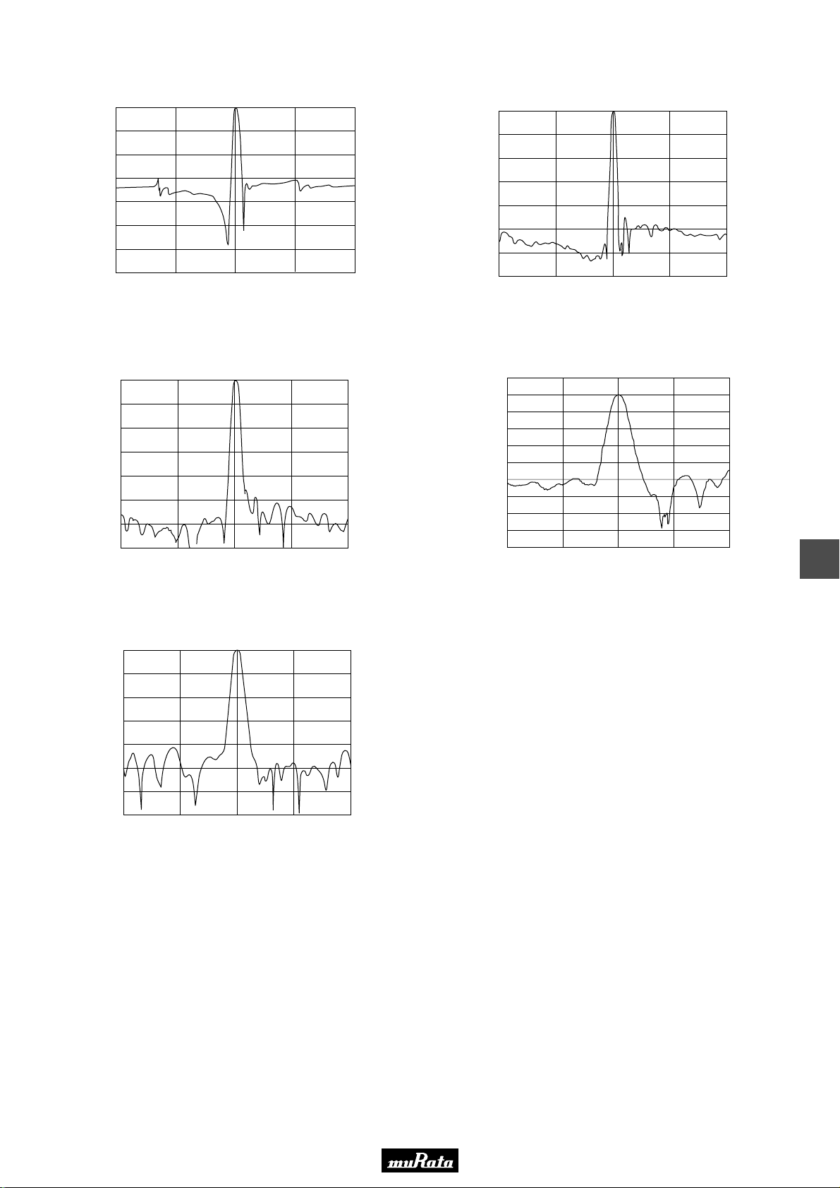
■ Frequency Characteristics (Spurious)
0
10
20
30
40
Attenuation ( dB )
50
60
70
9.700
10.200
10.700
Frequency ( MHz )
11.200
11.700
0
10
20
30
40
Attenuation (dB)
50
60
70
8.700 9.700 10.700 11.700 12.700
SFKLA10M7NF00-B0
SFVLA10M7MF00-B0
Frequency (MHz)
P61E7.pdf 01.10.17
SFVLA10M7LF00-B0
0
10
20
30
40
Attenuation (dB)
50
60
70
8.700 9.700 10.700 11.700 12.700
Frequency (MHz)
SFELA10M7KAH0-B0
0
10
20
30
40
Attenuation (dB)
50
60
70
8.700 9.700 10.700 11.700 12.700
Frequency (MHz)
SFELA10M7LFTA01-B0
0
10
20
30
40
50
Attenuation (dB)
60
70
80
90
10.70010.2009.700
Frequency (MHz)
11.200
11.700
8
27
Page 29
Please read CAUTION and Notice in this catalog for safety. This catalog has only typical specifications. Therefore you are requested
to approve our product specification or to transact the approval sheet for product specification, before your ordering.
P61E7.pdf 01.10.17
Ceramic Filters (CERAFILr) for FM Receivers
CERAFILr For FM -IF Tuners
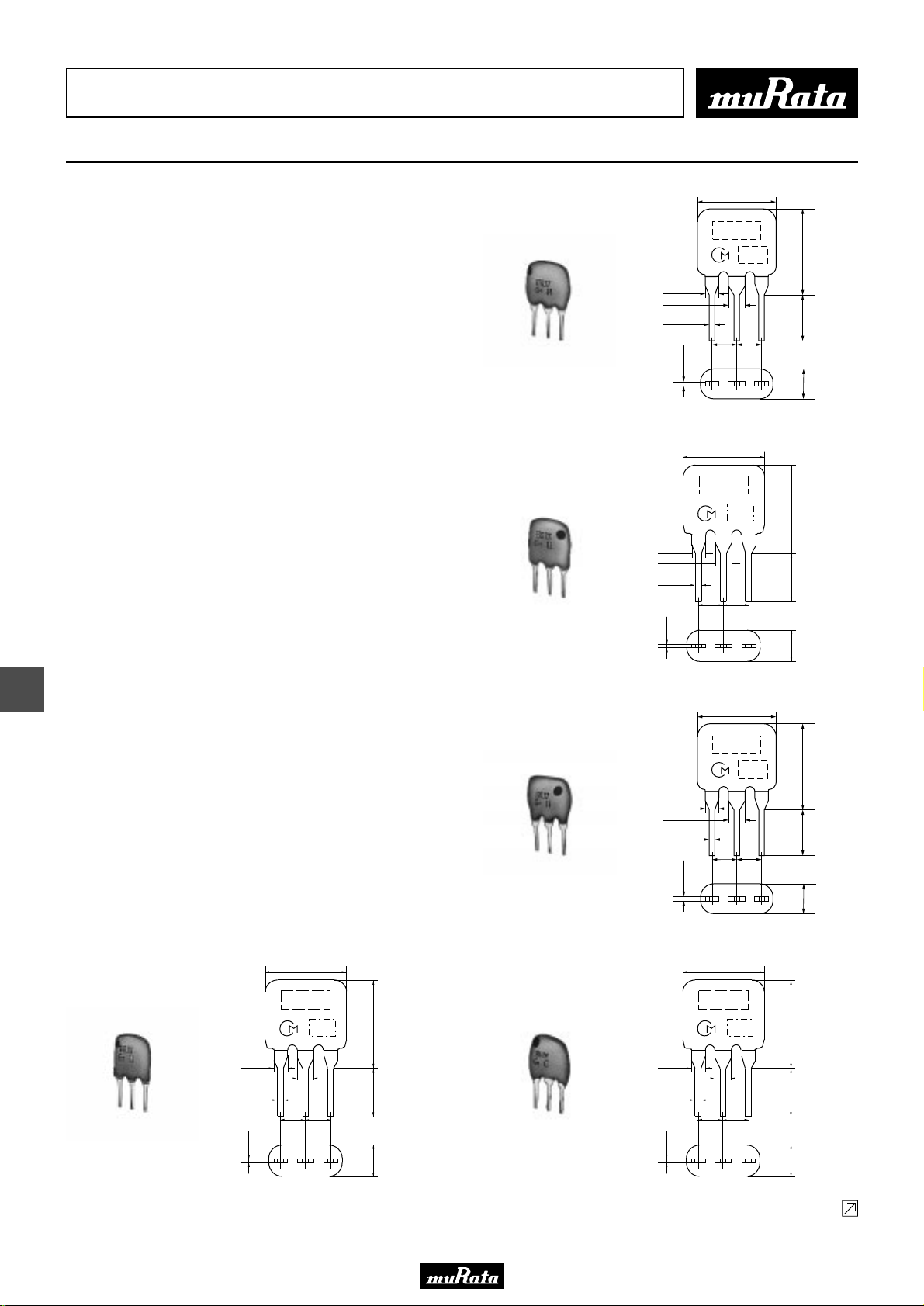
9.0 max.
SFELA10M7 series for FM-receivers are monolithic type
ceramic filters which use the energy trapped thickness
vibration-mode of the piezoelectric ceramic.
■ Features
1. Little dispersion of amplitude characteristics and
1.38±0.2
1.7±0.1
0.5±0.1
phase characteristics (G. D. T. characteristics).
2. The SFELA10M7G_X series has G. D. T characteristics
and is useful for obtaining low distortion.
SFELA10M7JAXE-B0
SFELA10M7F_L series, in these ceramic filters,
being in harmony with flatness of G. D. T. ,
roundness of the amplitude and selectivity
characteristics, therefore, these ceramic filters
are suitable to high-grade stereo tuners. Even if
mismatching condition, they can keep little
distortion because of low Qm of ceramic material.
The SFELA10M7FA0G series is based on
SFELA10M7FA00/GA00/HA00, and it obtains high
selectivity with low loss.
1.38±0.2
1.7±0.1
0.5±0.1
There is little dispersion of amplitude and
G. D. T. characteristics, and low distortion rate
can be obtained.
SFELA10M7HA0G-B0
0.3±0.1
3. All products are inspected for symmetry and
roundness of amplitude characteristics, and the
9
flatness of G. D. T. characteristics.
0.3±0.1
M A R K I N G
2.5±0.2
(3)
MARKING
EIAJ
CODE
2.5±0.2 2.5±0.2
(3) (2) (1)
7.0±2.0
E I A J
C O D E
2.5±0.2
(1)
(2)
9.0 max.
7.0±2.0
5.0±1.0
3.0±1.0
10.0 max.5.0±1.0
4.0 max.
(1) : Input
(2) : Ground
(3) : Output
(in mm)
SFELA10M7GA0G-B0
1.38±0.2
1.7±0.1
0.5±0.1
0.3±0.1
7.0±2.0
M A R K I N G
2.5±0.2
(3)
(2)
E I A J
C O D E
2.5±0.2
MARKING
EIAJ
CODE
1.38±0.2
1.7±0.1
0.5±0.1
2.5±0.2 2.5±0.2
1.38±0.2
1.7±0.1
0.5±0.1
0.3±0.1
0.3±0.1
M A R K I N G
2.5±0.2
(3)
(3) (2) (1)
7.0±2.0
E I A J
C O D E
2.5±0.2
(1)
(2)
SFELA10M7HAXD-B0
7.0±2.0
5.0±1.0
(1) : Input
(2) : Ground
(3) : Output
3.0±1.0
(1)
(in mm)
SFELA10M7GALM-B0
7.0±2.0
5.0±1.0
3.0±1.0
10.0 max.5.0±1.0
4.0 max.
(1) : Input
(2) : Ground
(3) : Output
(in mm)
Continued on the following page.
28
Page 30
Please read CAUTION and Notice in this catalog for safety. This catalog has only typical specifications. Therefore you are requested
to approve our product specification or to transact the approval sheet for product specification, before your ordering.
Continued from the preceding page.
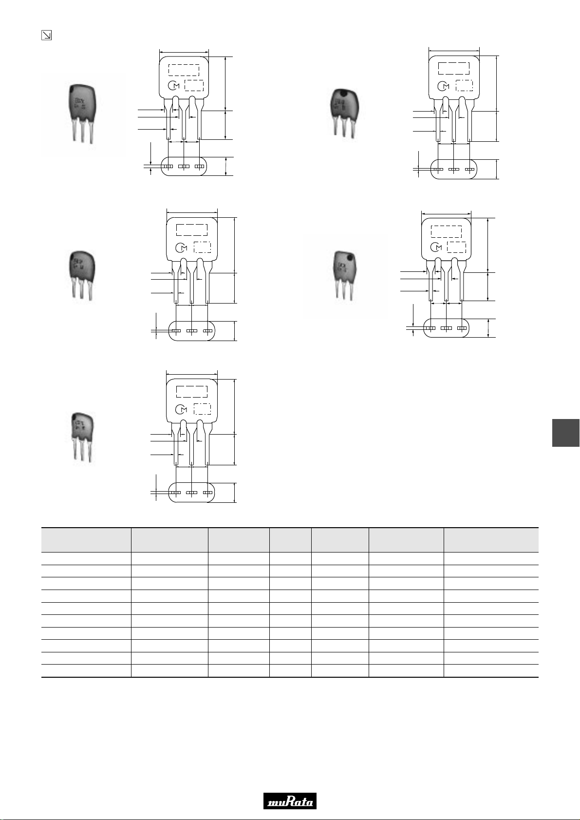
9.0 max.
P61E7.pdf 01.10.17
7.0±2.0
SFELA10M7GAXA-B0
SFELA10M7GALP03-B0
1.38±0.2
1.7±0.1
0.5±0.1
0.3±0.1
1.38±0.2
1.7±0.1
MARKING
2.5±0.2 2.5±0.2
(3) (2) (1)
0.5±0.1
0.3±0.1
(3)
EIAJ
CODE
7.0±2.0
M A R K I N G
E I A J
C O D E
2.5±0.2
2.5±0.2
(2)
M A R K I N G
E I A J
2.5±0.2
2.5±0.2
(3)
(2)
9.0 max.
MARKING
EIAJ
CODE
2.5±0.2 2.5±0.2
C O D E
11.0 max.5.0±1.0
1.38±0.2
1.7±0.1
0.5±0.1
(1) : Input
(2) : Ground
(3) : Output
4.0 max.
(1)
7.0±2.0
5.0±1.0
3.0±1.0
in mm
(1) : Input
(2) : Ground
(3) : Output
(in mm)
SFELA10M7FA0G-B0
SFELA10M7GAXX-B0
1.38±0.2
1.7±0.1
0.5±0.1
0.3±0.1
0.3±0.1
(3) (2) (1)
7.0±2.0
5.0±1.0
(1) : Input
(2) : Ground
(3) : Output
3.0±1.0
(1)
(in mm)
11.0 max.5.0±1.0
(1) : Input
(2) : Ground
(3) : Output
4.0 max.
in mm
7.0±2.0
M A R K I N G
E I A J
SFELA10M7FALL-B0
Part Number
C O D E
1.38±0.2
1.7±0.1
0.5±0.1
2.5±0.2
2.5±0.2
0.3±0.1
(3)
(2)
Center Frequency (fo)
(MHz)
7.0±2.0
5.0±1.0
3.0±1.0
(1)
3dB Bandwidth
(kHz)
(1) : Input
(2) : Ground
(3) : Output
(in mm)
Attenuation
(kHz)
Insertion Loss
(dB)
Spurious Attenuation
(dB)
GDT Bandwidth
(kHz)
SFELA10M7JAXE-B0 10.700 ±30kHz within150 ±30kHz 500 max. 14.0 max. 35 min. fo±50 min.[within 0.15µsec.]
SFELA10M7HA0G-B0 10.700 ±30kHz within180 ±40kHz 520 max. 7.0 max. 40 min. fo±45 min.[within 0.5µsec.]
SFELA10M7HAXD-B0 10.700 ±30kHz within180 ±30kHz 530 max. 14.0 max. 33 min. fo±60 min.[within 0.15µsec.]
SFELA10M7GA0G-B0 10.700 ±30kHz within230 ±50kHz 600 max. 7.0 max. 40 min. fo±60 min.[within 0.5µsec.]
SFELA10M7GALM-B0 10.700 ±30kHz within230 ±50kHz 600 max. within9.0 ±2.0dB 30 min. fo±60 min.[within 0.25µsec.]
SFELA10M7GAXA-B0 10.700 ±30kHz within220 ±40kHz 610 max. 12.5 max. 30 min. fo±80 min.[within 0.15µsec.]
SFELA10M7FA0G-B0 10.700 ±30kHz within280 ±50kHz 650 max. within4.0 ±2.0dB 30 min. fo±85 min.[within 0.5µsec.]
SFELA10M7GALP03-B0 10.700 ±30kHz within250 ±50kHz 650 max. 10.0 max. 30 min. fo±65 min.[within 0.25µsec.]
SFELA10M7GAXX-B0 10.700 ±30kHz within250 ±40kHz 670 max. 12.0 max. 25 min. fo±110 min.[within 0.2µsec.]
SFELA10M7FALL-B0 10.700 ±30kHz within280 ±50kHz 700 max. within7.0 ±2.0dB 25 min. fo±70 min.[within 0.25µsec.]
Area of Attenuation : [within 20dB] Area of Spurious Attenuation : [within 9MHz to 12MHz]
Center frequency(fo) defined by the center of 3dB bandwidth.
9
29
Page 31
Please read CAUTION and Notice in this catalog for safety. This catalog has only typical specifications. Therefore you are requested
to approve our product specification or to transact the approval sheet for product specification, before your ordering.
■ Center Frequency Rank Code
CODE
D
B
A
C
E
Z
M
30kHz Step
10.64MHz±30kHz
10.67MHz±30kHz
10.70MHz±30kHz
10.73MHz±30kHz
10.76MHz±30kHz
Combination A,B,C,D,E
Combination A,B,C
25kHz Step
10.650MHz±25kHz
10.675MHz±25kHz
10.700MHz±25kHz
10.725MHz±25kHz
10.750MHz±25kHz
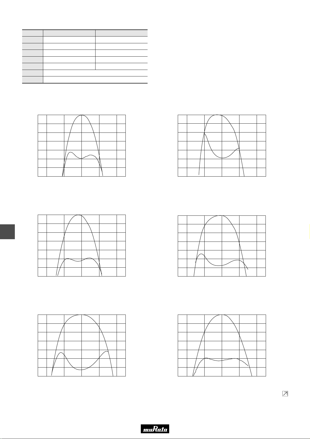
■ Freq. Characteristics
SFELA10M7JAXE-B0
0 5.00
1 4.75
2 4.50
3 4.25
4 4.00
Attenuation (dB)
5 3.75
6 3.50
7 3.25
10.500 10.600 10.700 10.800 10.900
Frequency (MHz)
0 6.00
1 5.50
2 5.00
3 4.50
G.D.T. (µsec.)
4 4.00
Attenuation (dB)
5 3.50
6 3.00
7 2.50
10.500 10.600 10.700 10.800 10.900
SFELA10M7HA0G-B0
Frequency (MHz)
P61E7.pdf 01.10.17
G.D.T. (µsec.)
SFELA10M7HAXD-B0
0 4.50
1 4.25
9
2 4.00
3 3.75
4 3.50
Attenuation (dB)
5 3.25
6 3.00
7 2.75
10.500 10.600 10.700 10.800 10.900
Frequency (MHz)
G.D.T. (µsec.)
0 6.00
1 5.50
2 5.00
3 4.50
4 4.00
Attenuation (dB)
5 3.50
6 3.00
7 2.50
10.500 10.600 10.700 10.800 10.900
SFELA10M7GALM-B0
0 4.00
1 3.75
2 3.50
3 3.25
4 3.00
Attenuation (dB)
5 2.75
6 2.50
7 2.25
10.500 10.600 10.700 10.800 10.900
Frequency (MHz)
G.D.T. (µsec.)
0 3.75
1 3.50
2 3.25
3 3.00
4 2.75
Attenuation (dB)
5 2.50
6 2.25
7 2.00
10.500 10.600 10.700 10.800 10.900
SFELA10M7GA0G-B0
G.D.T. (µsec.)
Frequency (MHz)
SFELA10M7GAXA-B0
G.D.T. (µsec.)
Frequency (MHz)
30
Continued on the following page.
Page 32
Please read CAUTION and Notice in this catalog for safety. This catalog has only typical specifications. Therefore you are requested
to approve our product specification or to transact the approval sheet for product specification, before your ordering.
Continued from the preceding page.
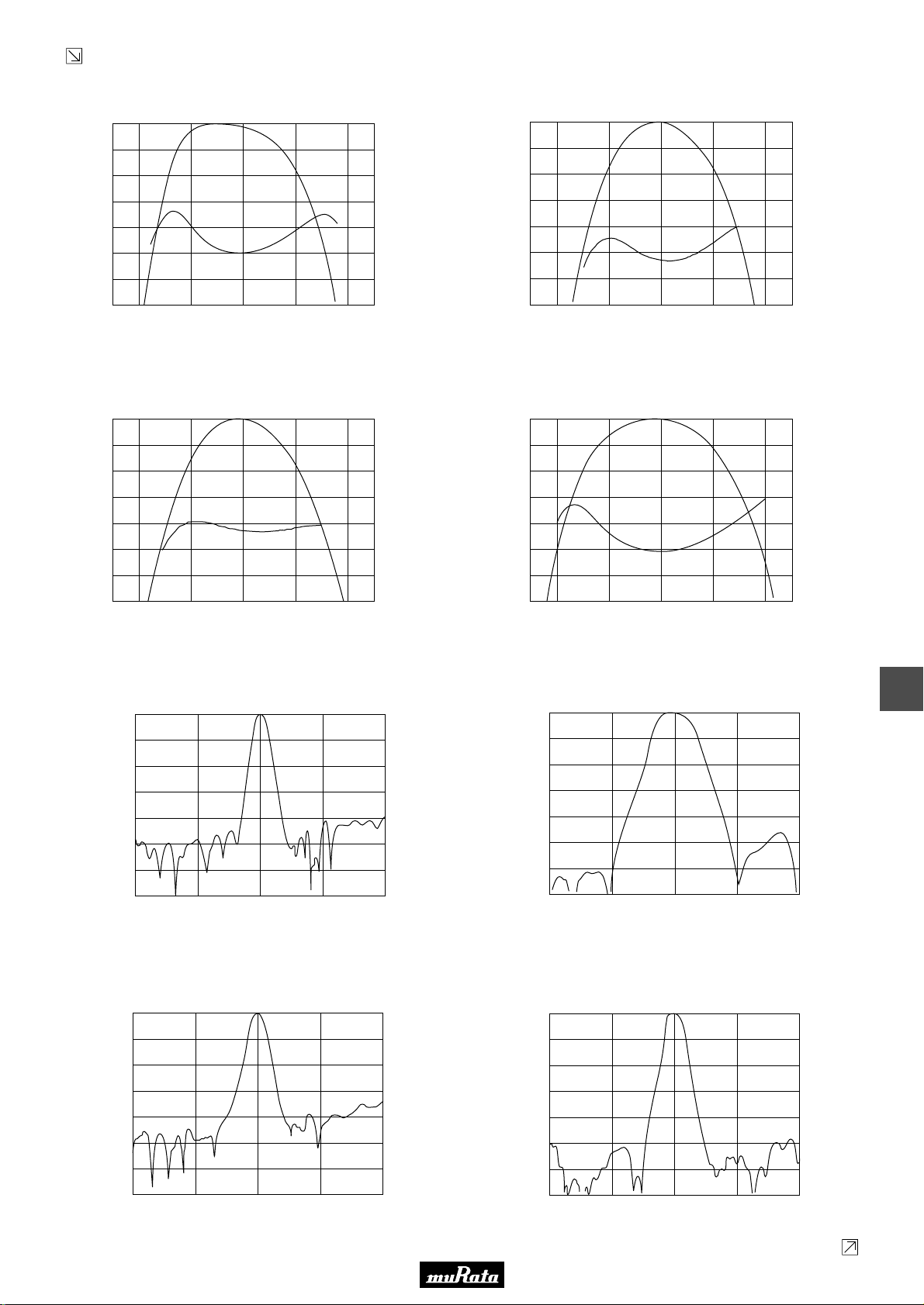
■ Freq. Characteristics
SFELA10M7FA0G-B0
0 5.00
1 4.50
2 4.00
3 3.50
4 3.00
Attenuation (dB)
5 2.50
6 2.00
7 1.50
10.500 10.600 10.700 10.800 10.900
Frequency (MHz)
0 3.75
1 3.50
2 3.25
3 3.00
G.D.T. (µsec.)
4 2.75
Attenuation (dB)
5 2.50
6 2.25
7 2.00
10.500 10.600 10.700 10.800 10.900
SFELA10M7GALP03-B0
Frequency (MHz)
P61E7.pdf 01.10.17
G.D.T. (µsec.)
SFELA10M7GAXX-B0
0 3.25
1 3.00
2 2.75
3 2.50
4 2.25
Attenuation (dB)
5 2.00
6 1.75
7 1.50
10.500 10.600 10.700 10.800 10.900
Frequency (MHz)
■ Spurious Frequency
SFELA10M7JAXE-B0
0
10
20
30
40
Attenuation (dB)
50
60
70
8.700 9.700 10.700 11.700 12.700
Frequency (MHz)
SFELA10M7FALL-B0
0 3.25
1 3.00
2 2.75
3 2.50
G.D.T. (µsec.)
4 2.25
Attenuation (dB)
5 2.00
6 1.75
7 1.50
10.500 10.600 10.700 10.800 10.900
Frequency (MHz)
SFELA10M7HA0G-B0
0
10
20
30
40
Attenuation (dB)
50
60
70
9.900 10.300 10.700 11.100 11.500
Frequency (MHz)
G.D.T. (µsec.)
9
SFELA10M7HAXD-B0
0
10
20
30
40
Attenuation (dB)
50
60
70
8.700 9.700 10.700 11.700 12.700
Frequency (MHz)
SFELA10M7GA0G-B0
0
10
20
30
40
Attenuation (dB)
50
60
70
8.700 9.700 10.700 11.700 12.700
Frequency (MHz)
Continued on the following page.
31
Page 33
Please read CAUTION and Notice in this catalog for safety. This catalog has only typical specifications. Therefore you are requested
to approve our product specification or to transact the approval sheet for product specification, before your ordering.
Continued from the preceding page.
■ Spurious Frequency
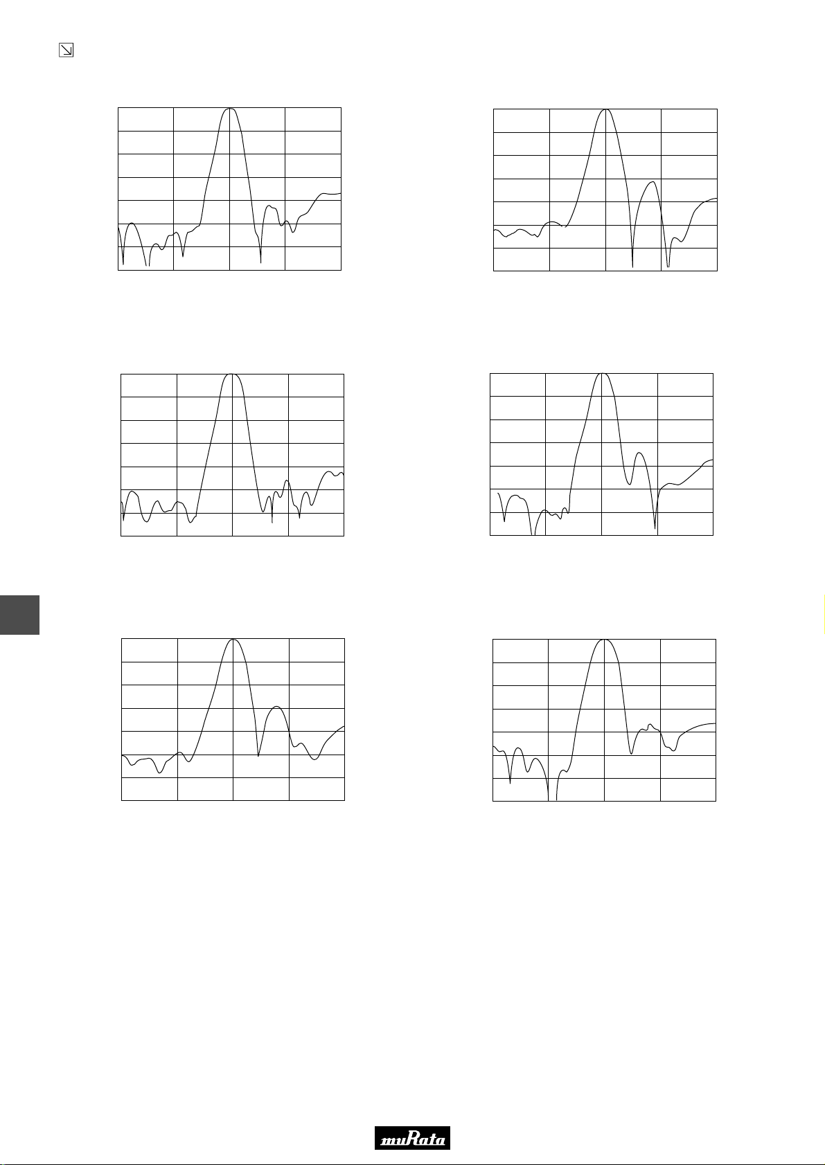
SFELA10M7GALM-B0
0
10
20
30
40
Attenuation (dB)
50
60
70
8.700 9.700 10.700 11.700 12.700
Frequency (MHz)
0
10
20
30
40
Attenuation (dB)
50
60
70
8.700 9.700 10.700 11.700 12.700
SFELA10M7GAXA-B0
P61E7.pdf 01.10.17
Frequency (MHz)
SFELA10M7FA0G-B0
0
10
20
30
40
Attenuation (dB)
50
60
70
8.700 9.700 10.700 11.700 12.700
9
0
10
20
30
40
Attenuation (dB)
50
60
70
8.700 9.700 10.700 11.700 12.700
Frequency (MHz)
SFELA10M7GAXX-B0
Frequency (MHz)
0
10
20
30
40
Attenuation (dB)
50
60
70
8.700 9.700 10.700 11.700 12.700
0
10
20
30
40
Attenuation (dB)
50
60
70
8.700 9.700 10.700 11.700 12.700
SFELA10M7GALP03-B0
Frequency (MHz)
SFELA10M7FALL-B0
Frequency (MHz)
32
Page 34
Please read CAUTION and Notice in this catalog for safety. This catalog has only typical specifications. Therefore you are requested
to approve our product specification or to transact the approval sheet for product specification, before your ordering.
Ceramic Filters (CERAFILr) for FM Receivers
CERAFILr Three-Elements Type SFTLA Series
SFTLA10M7 series for FM-receivers are monolithic type
ceramic filters which use the energy trapped thickness
vibration-mode of the piezoelectric ceramic.
■ Features
1. It has an excellent shape factor, and it is
possible to obtain 1.5 times more excellent
selectivity than SFELA10M7 series (by detuning
+-300 or 400kHz).
2. Good performance of spurious suppression.
3. Having the same terminal pitch as the SFELA10M7
series, it easily replaces that series.
4. By replacing two SFELA10M7 series filters with one
SFTLA10M7 filter,more compact sets can be made.
5. Well-suited for 1-chip ICs.
SFTLA10M7HA00-B0
0.4±0.1
0.65±0.1
1.4±0.1
0.5±0.1
0.3±0.1
0.4±0.1
0.65±0.1
1.4±0.1
0.5±0.1
10.0±1.0
M A R K I N G
E I A J
C O D E
2.5±0.2
2.5±0.2
10.0±1.0
M A R K I N G
E I A J
C O D E
P61E7.pdf 01.10.17
6.0±1.0
5.0±1.0
(1) : Input
(2) : Ground
(3) : Output
(1)(2)(3)
3.0±1.0
6.0±1.0
5.0±1.0
in mm
2.5±0.2
2.5±0.2
0.3±0.1
0.4±0.1
0.65±0.1
1.4±0.1
0.5±0.1
0.3±0.1
Insertion Loss
(dB)
(1)(2)(3)
10.0±1.0
M A R K I N G
E I A J
C O D E
2.5±0.2
2.5±0.2
(1)(2)(3)
Spurious Attenuation
3.0±1.0
6.0±1.0
5.0±1.0
3.0±1.0
(dB)
Part Number
Center Frequency (fo)
(MHz)
3dB Bandwidth
(kHz)
SFTLA10M7GA00-B0
SFTLA10M7FA00-B0
Attenuation
(kHz)
SFTLA10M7HA00-B0 10.700 ±30kHz within180 ±40kHz 550 max. within5.5 ±2.5dB 50 min.
SFTLA10M7GA00-B0 10.700 ±30kHz within230 ±40kHz 650 max. within6.0 ±2.0dB 50 min.
SFTLA10M7FA00-B0 10.700 ±30kHz within280 ±50kHz 700 max. within6.0 ±2.0dB 50 min.
Area of Attenuation : [within 40dB] Area of Spurious Attenuation : [within 9MHz to 12MHz]
Center frequency(fo) defined by the center of 3dB bandwidth.
(1) : Input
(2) : Ground
(3) : Output
in mm
(1) : Input
(2) : Ground
(3) : Output
in mm
10
33
Page 35
Please read CAUTION and Notice in this catalog for safety. This catalog has only typical specifications. Therefore you are requested
to approve our product specification or to transact the approval sheet for product specification, before your ordering.
■ Center Frequency Rank Code
CODE
D
B
A
C
E
Z
M
30kHz Step
10.64MHz±30kHz
10.67MHz±30kHz
10.70MHz±30kHz
10.73MHz±30kHz
10.76MHz±30kHz
Combination A,B,C,D,E
Combination A,B,C
25kHz Step
10.650MHz±25kHz
10.675MHz±25kHz
10.700MHz±25kHz
10.725MHz±25kHz
10.750MHz±25kHz
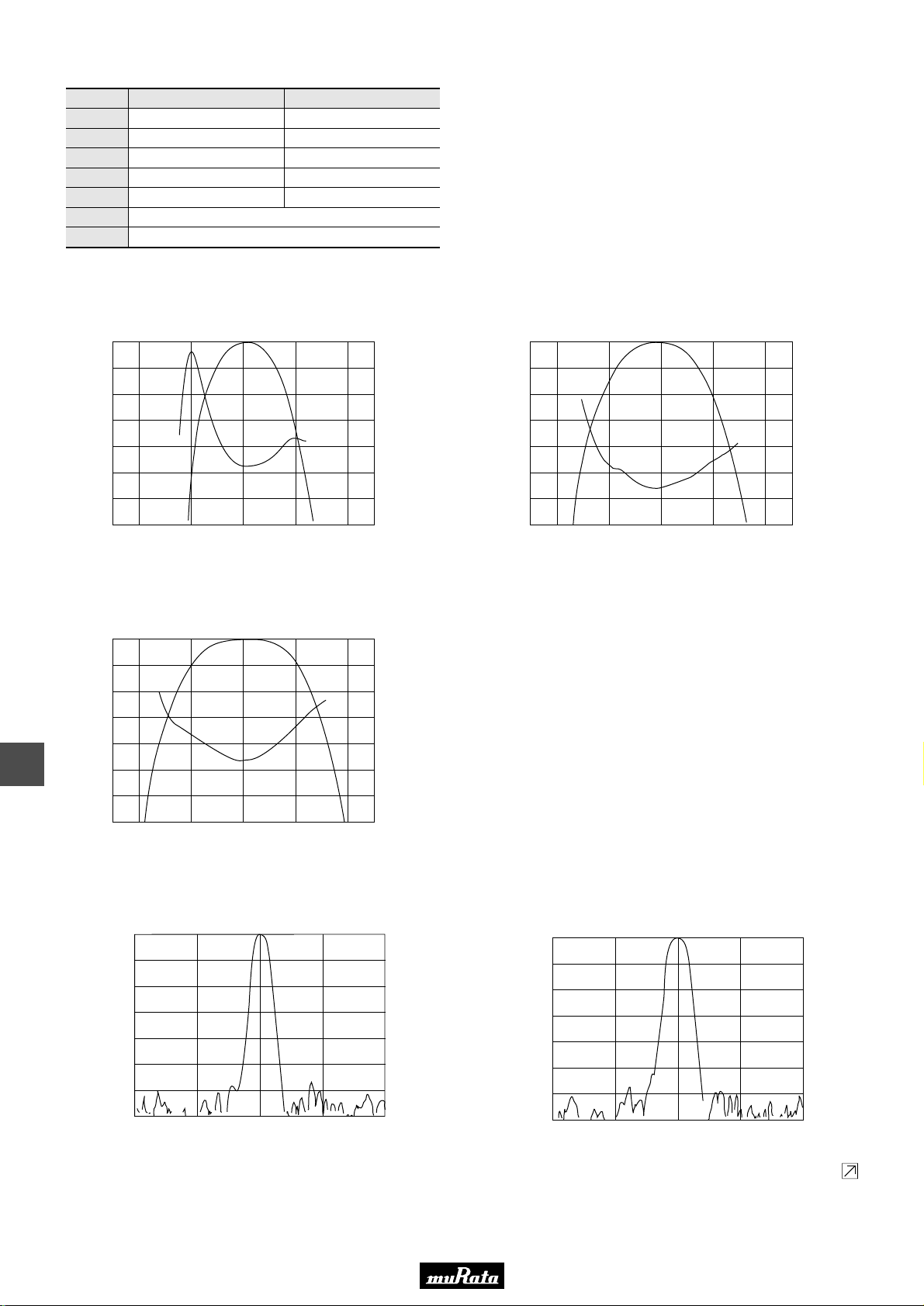
■ Frequency Characteristics
SFTLA10M7HA00-B0
0 8.00
1 7.50
2 7.00
3 6.50
4 6.00
Attenuation (dB)
5 5.50
6 5.00
7 4.50
10.500 10.600 10.700 10.800 10.900
Frequency (MHz)
0 7.00
1 6.50
2 6.00
3 5.50
G.D.T. (µsec.)
4 5.00
Attenuation (dB)
5 4.50
6 4.00
7 3.50
10.500 10.600 10.700 10.800 10.900
SFTLA10M7GA00-B0
Frequency (MHz)
P61E7.pdf 01.10.17
G.D.T. (µsec.)
10
SFTLA10M7FA00-B0
0 6.00
1 5.50
2 5.00
3 4.50
4 4.00
Attenuation (dB)
5 3.50
6 3.00
7 2.50
10.500 10.600 10.700 10.800 10.900
Frequency (MHz)
■ Frequency Characteristics (Spurious)
SFTLA10M7HA00-B0
0
10
20
30
40
Attenuation (dB)
50
60
70
8.700 9.700 10.700 11.700 12.700
Frequency (MHz)
G.D.T. (µsec.)
SFTLA10M7GA00-B0
0
10
20
30
40
Attenuation (dB)
50
60
70
8.700 9.700 10.700 11.700 12.700
Frequency (MHz)
34
Continued on the following page.
Page 36
Please read CAUTION and Notice in this catalog for safety. This catalog has only typical specifications. Therefore you are requested
to approve our product specification or to transact the approval sheet for product specification, before your ordering.
Continued from the preceding page.
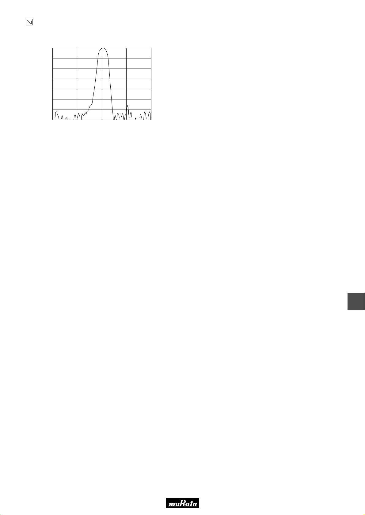
■ Frequency Characteristics (Spurious)
SFTLA10M7FA00-B0
0
10
20
30
40
Attenuation (dB)
50
60
70
8.700 9.700 10.700 11.700 12.700
Frequency (MHz)
P61E7.pdf 01.10.17
10
35
Page 37
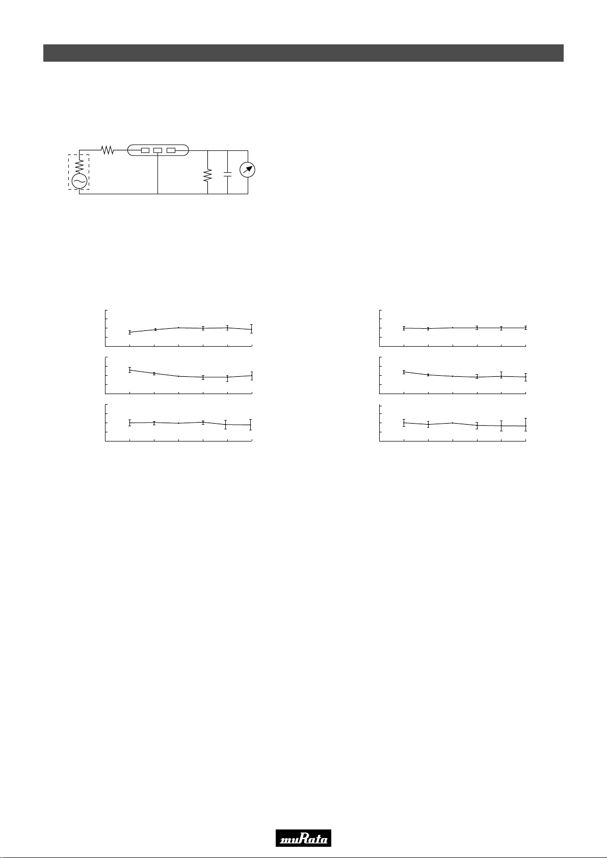
Please read CAUTION and Notice in this catalog for safety. This catalog has only typical specifications. Therefore you are requested
to approve our product specification or to transact the approval sheet for product specification, before your ordering.
Lead Type CERAFILr Test Circuit and Characteristics Data
■ Test Circuit
(1) : Input
(2) : Output
1
R
(1) (2) (3)
(3) :Ground
P61E7.pdf 01.10.17
Rg
S.S.G
Rg + R1 = R2 = 330Ω
C = 10pF (Including stray capacitance and input
capacitance of RF voltmeter.)
■ Temperature Characteristics
W40
Center frequency
W20
0
Y20
Variation (kHz)Variation (dB)Variation (kHz)
Y40
Y20
W2
Insertion loss
W1
0
Y1
Y2
Y20
W40
3dB Band width
W20
0
Y20
Y40
Y20
SFELA10M7GA00-B0
0 W20
Temperature (˚C)
0 W20
Temperature (˚C)
0 W20
Temperature (˚C)
C
R2
W40 W60 W80
W40 W60 W80
W40 W60 W80
RF
Voltmeter
Variation (kHz)Variation (dB)Variation (kHz)
W40
W20
0
Y20
Y40
W2
W1
0
Y1
Y2
W40
W20
0
Y20
Y40
Center frequency
Y20
Insertion loss
Y20
3dB Band width
Y20
SFELA10M7HA00-B0
0 W20 W40 W60 W80
Temperature (˚C)
0 W20 W40 W60 W80
Temperature (˚C)
0 W20 W40 W60 W80
Temperature (˚C)
10
■ Matching Conditions
•When using ceramic filters, it is most important to
match the input/output load to impedance 330 ohm
(only SFELA10M7DF00-B0 is 470 ohm matching).
Waveform symmetry is damaged when reactance
is added to the input/output load.
•Two ceramic filters directly connected can be used
for high selelctivity. For reducing waveform
variation, it is recommended to input a buffer AMP
between ceramic filters.
•The SFELA10M7 and SFTLA10M7 series are of
input/output symmetric structure so that in theory
there is no input/output directionality. Actual
circuits may use different input/output loading
conditions (for example, mismatched impedance) or
capacitance load. In such cases, the waveform will
be a little changed by the direction of the
input/output of the ceramic filters.
36
Page 38
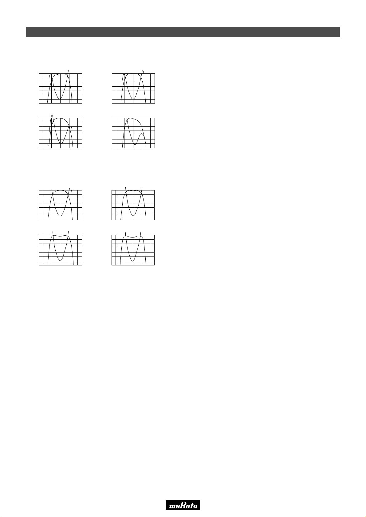
Please read CAUTION and Notice in this catalog for safety. This catalog has only typical specifications. Therefore you are requested
to approve our product specification or to transact the approval sheet for product specification, before your ordering.
Lead Type CERAFILr Characteristics Data and Notice
■ Loaded Resistance and Waveform (Rg+R1=330ohm)
R2=220Ω R2=330Ω
0 1.2
1
2
3
4
5
Attenuation (dB)Attenuation (dB)
6
7
0 1.2
1
2
3
4
5
6
7
10.7 10.8 10.910.610.5
Frequency (MHz)
2=560Ω R2=1kΩ
R
10.7 10.8 10.910.610.5
Frequency (MHz)
■ Loaded Capacitance and Waveform (Rg+R1=R2=330ohm)
C=10pF C=33pF
0 1.2
1
2
3
4
5
Attenuation (dB)Attenuation (dB)
6
7
0 1.2
1
2
3
4
5
6
7
10.7 10.8 10.910.610.5
Frequency (MHz)
C=56pF C=82pF
10.7 10.8 10.910.610.5
Frequency (MHz)
SFELA10M7GA00-B0
1.0
0.8
0.6
0.4
0.2
0
1.0
0.8
0.6
0.4
0.2
0
0 1.2
1
2
3
4
5
Attenuation (dB)Attenuation (dB)
6
7
Group Delay Time (µsec.)Group Delay Time (µsec.)
0 1.2
1
2
3
4
5
6
7
SFELA10M7GA00-B0
1.0
0.8
0.6
0.4
0.2
0
1.0
0.8
0.6
0.4
0.2
0
0 1.2
1
2
3
4
5
Attenuation (dB)Attenuation (dB)
6
7
Group Delay Time (µsec.)Group Delay Time (µsec.)
0 1.2
1
2
3
4
5
6
7
10.7 10.8 10.910.610.5
Frequency (MHz)
10.7 10.8 10.910.610.5
Frequency (MHz)
10.7 10.8 10.910.610.5
Frequency (MHz)
10.7 10.8 10.910.610.5
Frequency (MHz)
1.0
0.8
0.6
0.4
0.2
0
Group Delay Time (µsec.)Group Delay Time (µsec.)
1.0
0.8
0.6
0.4
0.2
0
1.0
0.8
0.6
0.4
0.2
0
Group Delay Time (µsec.)Group Delay Time (µsec.)
1.0
0.8
0.6
0.4
0.2
0
P61E7.pdf 01.10.17
■ Notice (Soldering and Mounting)
The component cannot be withstand washing.
■ Notice (Handling)
1. Do not use this product with bend. The component
may be damaged if excess mechanical stress is
applied to it mounted on the printed circuit board.
2. The component may be damaged when an excess stress
will be applied.
3. All kinds of re-flow soldering must not be applied
on the component.
4. Do not clean or wash the component as it is not
hermetically sealed.
5. Do not use strong acidity flux, more than 0.2wt%
10
chlorine content, in flow soldering.
6. In case of covering discriminator with over coat,
conditions such as material of resin, cure
temperature, and so on should be evaluated well.
7. Accurate test circuit values are required to
measure electrical characteristics. It may be a
cause of mis-correlation if there is any deviation,
especially stray capacitance, from the test
circuit in the specification.
37
Page 39
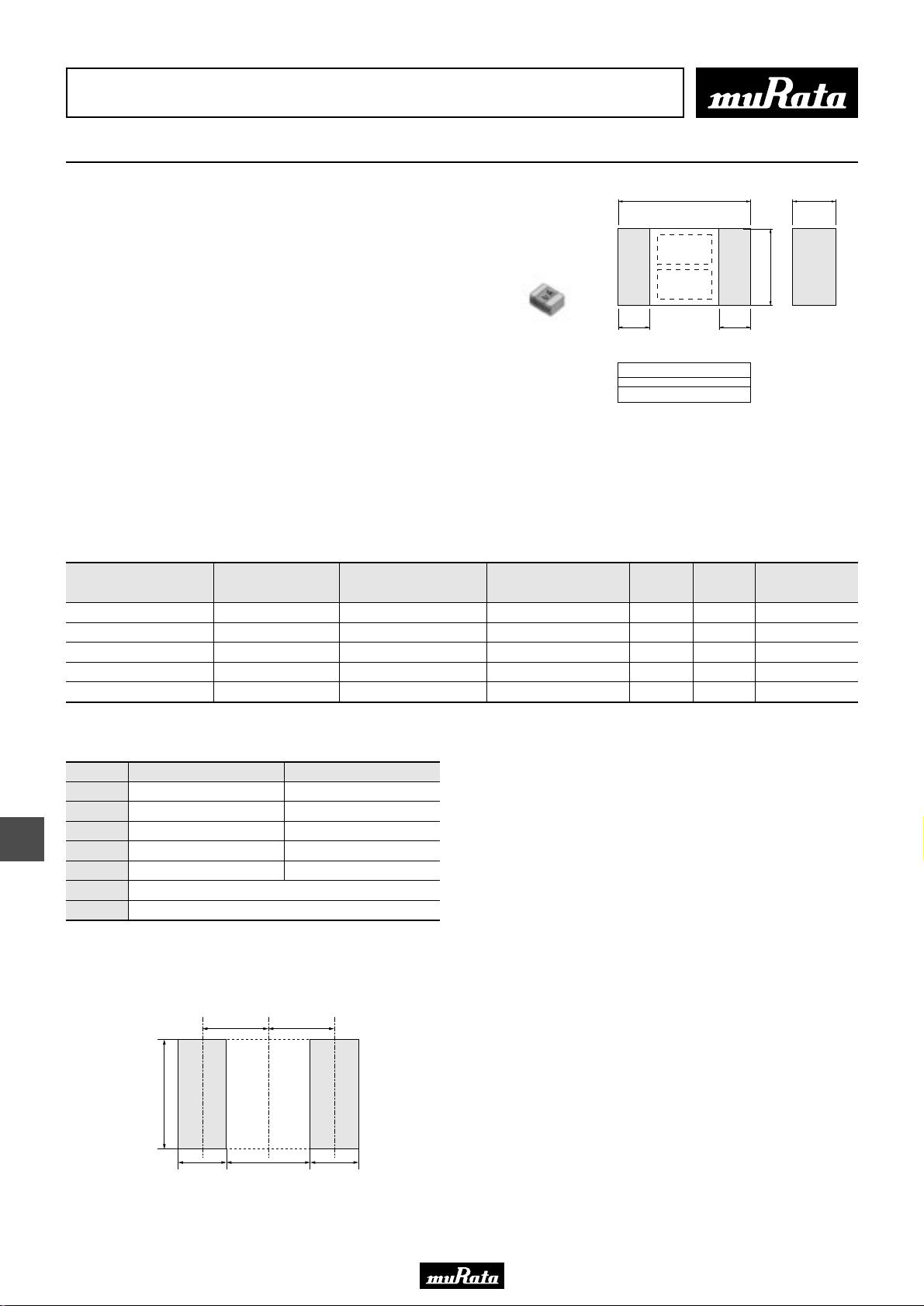
Please read CAUTION and Notice in this catalog for safety. This catalog has only typical specifications. Therefore you are requested
to approve our product specification or to transact the approval sheet for product specification, before your ordering.
Ceramic Filters (CERAFILr) for FM Receivers
Discriminators Chip Type CDACV Series
P61E7.pdf 01.10.17
3.4±0.5
1.5±0.3
CDACV10M7 series forms a resonator on a piezoelectric
ceramic substrate. In combination with ICs, this type
obtains stable demodulation characteristics in wide
bandwidths.
■ Features
0.9±0.3
∗ ∗∗
2.6±0.3
0.9±0.3
1. Compact and excellent mechanical strength.
2. Can be combined with various ICs. The IC is
determined by the last number in the part number.
3. Stable demodulation characteristics can be obtained
: EIAJ Monthly Code
∗
: Rank
∗∗
without adjustment.
4. The MG type for wide bandwidths and the MC type for
narrow bandwidths are available.
5. Stable temperature characteristics.
6. We recommend kits : ceramic discriminator
CDACV10M7 series and "CERAFIL" SFECV10M7 of the
same frequency rank.
Part Number
CDACV10M7GA001-R0 10.700 ±30kHz fo±150 min. 55 min. 1.0 max. CX20029 Quadrature
CDACV10M7GA016-R0 10.700 ±30kHz 300 min. within60 to 90mV 0.9 max. TA8122F Quadrature
CDACV10M7GA046-R0 10.700 ±30kHz 330 min. 280 min. 1.5 max. LA1832 Quadrature
CDACV10M7GA069-R0 10.700 ±30kHz 330 min. 80 min. 1.0 max. CXA1538N Quadrature
CDACV10M7CA001-R0 10.700 ±30kHz fo±150 min. 55 min. 1.0 max. CX20091 Quadrature
Center Frequency (fo)
(MHz)
Recovered Audio 3dB BW
(kHz)
Recovered Audio Output
(mV)
Distortion
(%)
IC Detection Method
in mm
11
■ Center Frequency Rank Code
CODE
D
B
A
C
E
Z
M
30kHz Step
10.64MHz±30kHz
10.67MHz±30kHz
10.70MHz±30kHz
10.73MHz±30kHz
10.76MHz±30kHz
Combination A,B,C,D,E
Combination A,B,C
10.650MHz±25kHz
10.675MHz±25kHz
10.700MHz±25kHz
10.725MHz±25kHz
10.750MHz±25kHz
■ Standard Land Pattern Dimensions
1.5
2.6
1.5
1.51.4 1.4
25kHz Step
38
Page 40
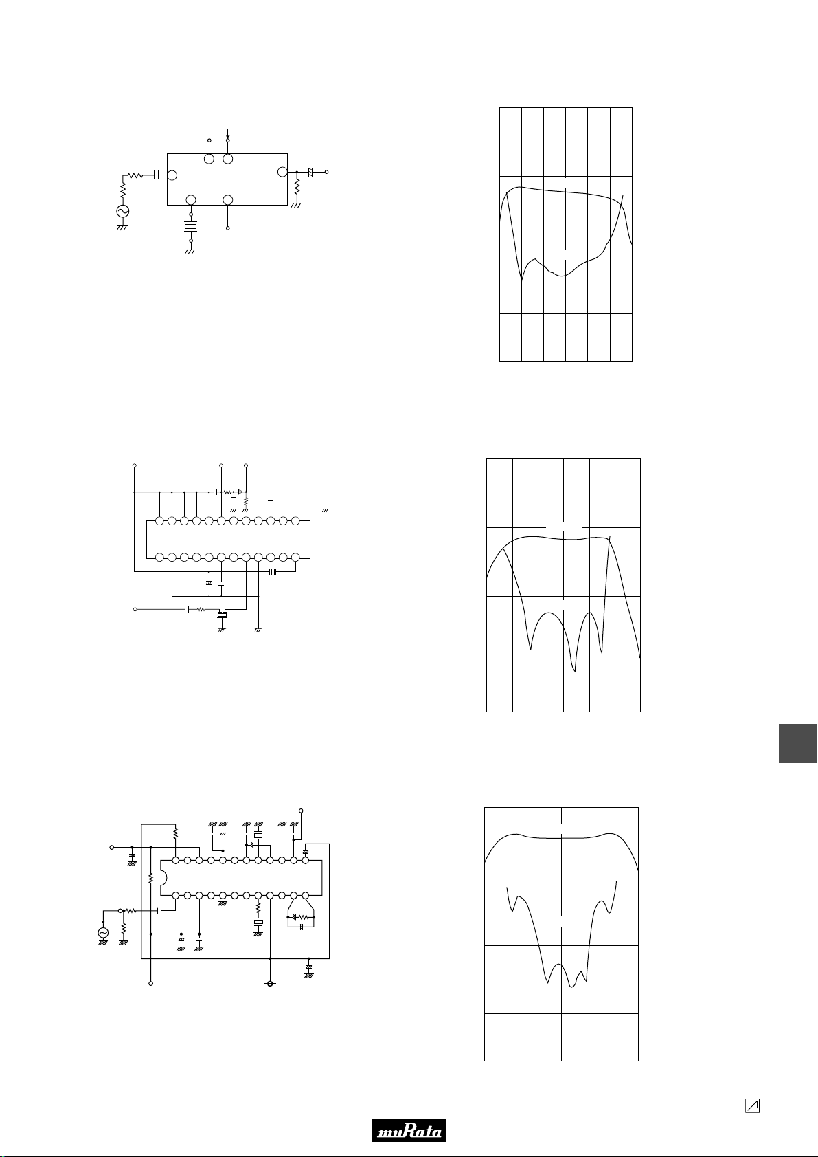
Please read CAUTION and Notice in this catalog for safety. This catalog has only typical specifications. Therefore you are requested
to approve our product specification or to transact the approval sheet for product specification, before your ordering.
■ CDACV10M7GA001-R0
Test Circuit
1000
AFC
REF
0.01µ
280
Fg=50
5 33
39
CX20029
289
1µ
+ –
100k
AF OUTPUT
100
32
Frequency Characteristics
AF Output
P61E7.pdf 01.10.17
100
10
S.S.G.
CDALA10M7GA001
■ CDACV10M7GA016-R0
Test Circuit
VCC +3V DC Out AF Out
24 23 22 21 20 19 18 17 16 15 14 13
TA8122F (TOSHIBA)
1 2 3 4 5 6 7 8 9 10 11 12
+
22µ
IF in
SFELA10M7DF00
270
0.022µ
Vcc=+3.0V
1k
330p
+
0.033µ
0.022µ
2.5µ
24k
CDACV10M7GA016
Unit
R : Ω
C : F
10
Recovered AF Output Voltage (mV)
1
10.4 10.5 10.6 10.8 10.9 11.010.7
Distortion
Frequency (MHz)
1
Distortion (%)
0.1
Input signal conditions
Input Level
Mod. Freq.
Freq.Dev.
100dBµ
1000Hz
±22.5kHz
Frequency Characteristics
1000
0.1µ
Unit
R : Ω
C : F
100
10
Recovered AF Output Voltage (mV)
1
10.510.4 10.6 10.7 10.8 10.9 11.0
AF Output
Distortion
Frequency (MHz)
100
10
1
Distortion (%)
0.1
Input signal conditions
Input Level
Mod. Freq.
Freq.Dev.
80dBµ
1000Hz
±22.5kHz
11
■ CDACV10M7GA046-R0
Test Circuit
6.8k
0.047µ
0.047µ5.6k
24 1314151617181920212223
LA1832 (SANYO)
1 12111098765432
CDALA10M7GA046
+
10µ
0.047µ
IF-IN
AFC
3.3µ
+
300
75
REG
CSBLA456KE2ZF15
1200p
+
22µ
+
1µ
270
Vcc (5V)
2.2µ
0.01µ
AF OUT
+
3k
1µ
0.01µ
1µ
+
100µ
Unit
R : Ω
C : F
Frequency Characteristics
1000
AF Output
100
Distortion
10
Recovered AF Output Voltage (mV)
1
10.510.4 10.6 10.7 10.8 10.9 11.0
Frequency (MHz)
100
10
1
Distortion (%)
0.1
Input signal conditions
Input Level
Mod. Freq.
Freq.Dev.
112dBµ
1000Hz
±75kHz
Continued on the following page.
39
Page 41
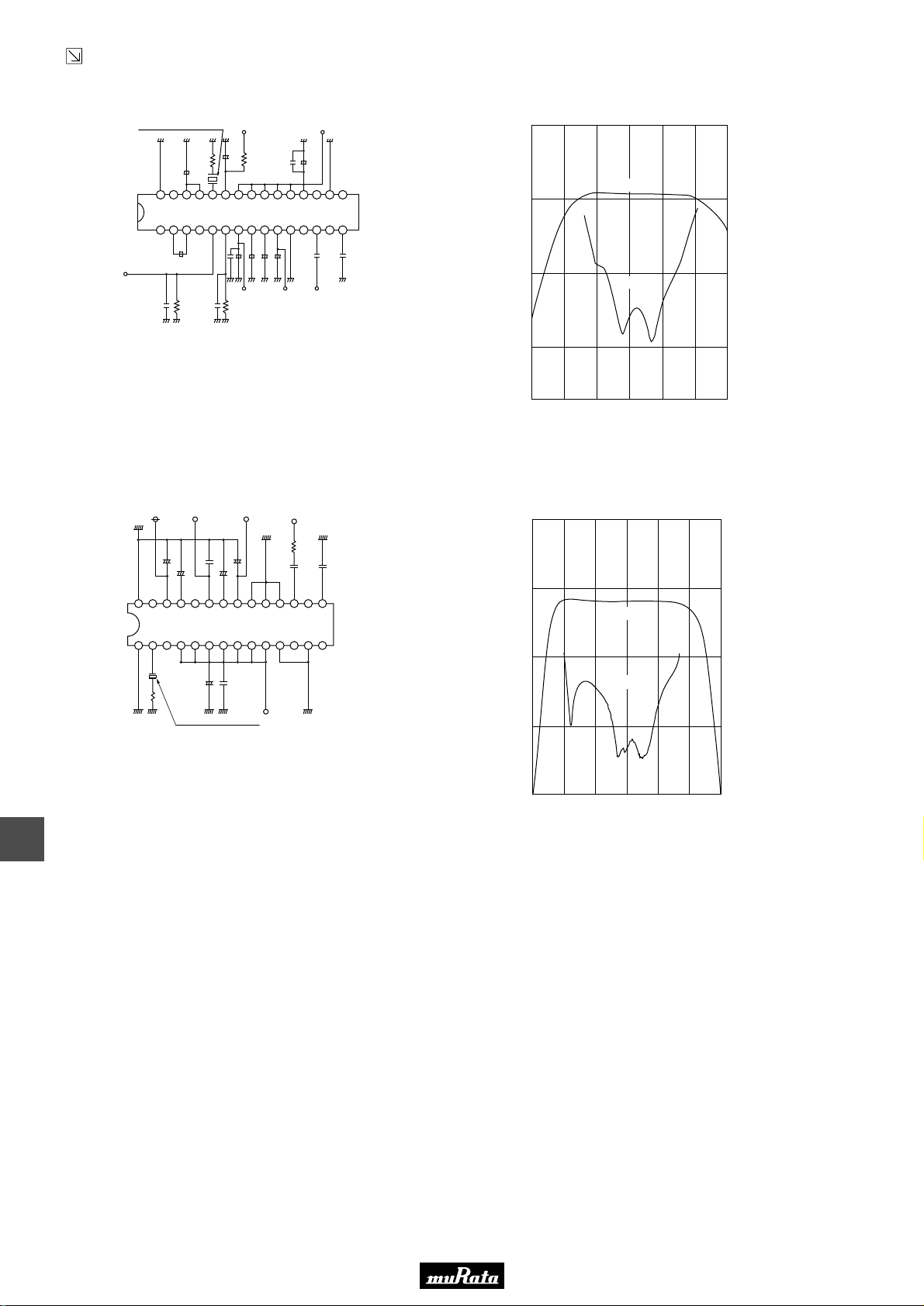
Please read CAUTION and Notice in this catalog for safety. This catalog has only typical specifications. Therefore you are requested
to approve our product specification or to transact the approval sheet for product specification, before your ordering.
Continued from the preceding page.
■ CDACV10M7GA069-R0
CDACV10M7GZ069-B0
AF OUT
0.022µ
100
10µ
+
30 2526272829
32 5 6 87 9 10
+
1µ
3.3k
0.022µ
Test Circuit
VCC (3V)
3.3µ
2.2k
+
CXA1538N
100 µ
0.01µ
+
VCC (3V) AFC
3.3k
Reg
10µ
0.01µ
+
22 21 20 18192324 17
11 1513
4.7µ
1µ
33µ
0.01µ 0.01µ
+ ++
IF IN
1000
16
141241
Unit
R : Ω
C : F
100
10
Recovered AF Output Voltage (mV)
1
Frequency Characteristics
AF Output
Distortion
10.510.4 10.6 10.7 10.8 10.9 11.0
Frequency (MHz)
P61E7.pdf 01.10.17
100
10
1
Distortion (%)
0.1
Input signal conditions
Input Level 100dBµ
Mod.Freq. 1000Hz
Freq.Dev. ±75kHz
11
■ CDACV10M7CA001-R0
Test Circuit
AF OUTVcc 3V
100µ
+
10µ
+
28 27 26 25 24 23 22 21 20 19 18 17 16 15
2 3 4 5 6 7 8 9 10 11 12 13 141
100
CDACV10M7CZ001-B0
+
4.7µ
10µ
0.022µ
+
CX20091 (SONY)
+
1000p
4.7µ
INPUTAFC OUT
REG OUT
S.S.G.(Rg=50)
280
0.01µ
0.01µ
Unit
R : Ω
C : F
Frequency Characteristics
1000
100
AF Output
10
Distortion
Recovered AF Output Voltage (mV)
1
10.510.4 10.6 10.7 10.8 10.9 11.0
Frequency (MHz)
10
10
1
Distortion (%)
0.1
Input signal conditions
Input Level 100dBµ
Mod.Freq. 1000Hz
Freq.Dev. ±22.5kHz
40
Page 42
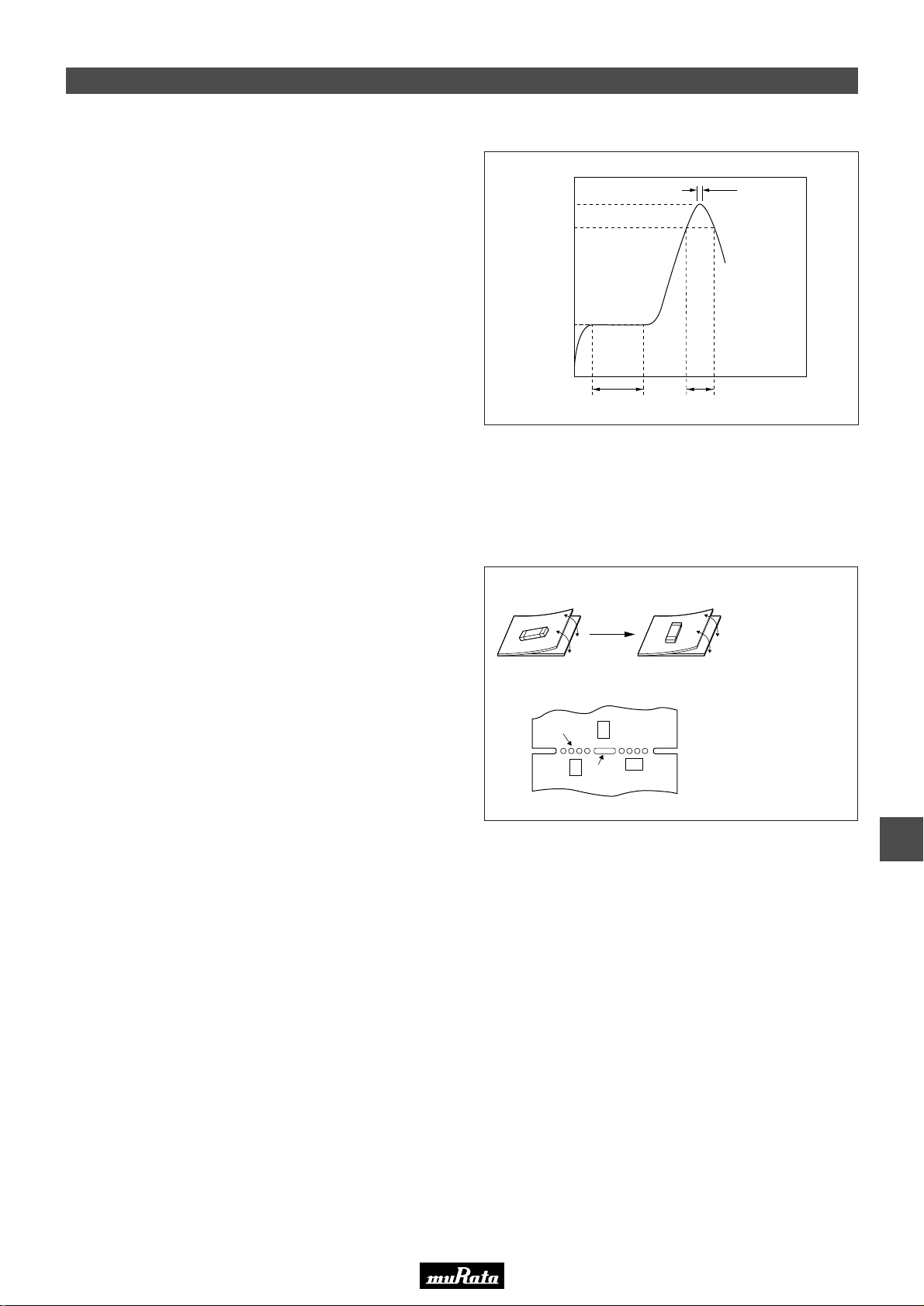
Please read CAUTION and Notice in this catalog for safety. This catalog has only typical specifications. Therefore you are requested
to approve our product specification or to transact the approval sheet for product specification, before your ordering.
Chip Type Discriminators CDACV Series Notice
■ Notice (soldering and mounting)
1. Standard Reflow Soldering Condition
(1) Reflow
240
230
Temperature (˚C)
150
P61E7.pdf 01.10.17
5sec.
Gradual
Cooling
(2) Soldering Iron
Lead terminal is directly contacted with the tip of
soldering iron of 280±5˚C for 3.0±0.5 seconds.
2. Wash
The component cannot be withstand washing.
■ Notice (handling)
1. The component may be damaged if excess mechanical
stress is applied to it mounted on the printed circuit
board.
2. Design layout of components on the PC board to
minimize the stress imposed on the warp or flexure of the
board.
3. After installing chips, if solder is excessively applied to
the circuit board, mechanical stress will cause destruction
resistance characteristics to lower. To prevent this, be
extremely careful in determining shape and dimension
before designing the circuit board diagram.
4. When the positioning claws and pick up nozzle are worn,
the load is applied to the chip while positioning is
concentrated to one positioning accuracy, etc. Careful
checking and maintenance are necessary to prevent
unexpected trouble.
5. When correcting chips with a soldering iron, the tip of the
soldering iron should not directly touch the chip
component. Depending on the soldering conditions, the
effective area of terminations may be reduced. the use of
solder containing Ag should be done to prevent the
electrode erosion.
6. Do not clean or wash the component as it is not
hermetically sealed.
7. In case of covering discriminator with over coat,
conditions such as material of resin, cure temperature,
and so on should be evaluated well.
8. Accurate test circuit values are required to measure
electrical characteristics.
It may be a cause of mis-correlation if there is any
deviation, especially stray capacitance, from the test
circuit in the specification.
60 30
[Component direction]
[Component layout close to board]
Perforation
B
A
C
Slit
Time (sec.)
Put the
component
lateral to the
direction in
which stress
acts.
Susceptibility to
stress is in the order
of : A>C>B
11
41
Page 43
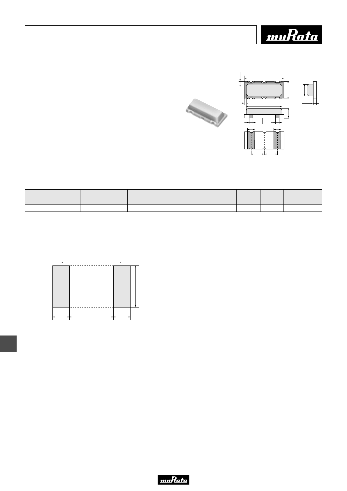
Please read CAUTION and Notice in this catalog for safety. This catalog has only typical specifications. Therefore you are requested
to approve our product specification or to transact the approval sheet for product specification, before your ordering.
Ceramic Filters (CERAFILr) for FM Receivers
Discriminators Chip Low-profile Type CDSCA Series
0.2
±
CDSCA10M7 series forms a resonator on a piezo electric
ceramic sabstrate. In combination with ICs, this type
obtains stable demoduration characteristics in wide
bandwidth.
0.3
0.2±0.2
4.5±0.1
4.1max
P61E7.pdf 01.10.17
2.0±0.1
1.4max
0.4±0.05
■ Features
1. Compact and high reliability and recommended for
0.4(ref.) 0.4(ref.)
1.2max
±
0.10.8±0.1
0.8
automotive applications.
2. Can be combined with various ICs. The IC is
determined by the last number in the part number.
1.5±0.1
1.5
±
0.1
3. Stable demoduration characteristics can be
obtained without adjustment.
4. Stable temperature characteristics.
5. Recommended for Pb free soldering.
Part Number
Center Frequency (fo)
(MHz)
CDSCA10M7GF107-R0 10.700 (fn) fn±80 min. 52 min. 3.0 max. TA31272F Quadrature
(fn) means nominal center frequency.
Recovered Audio 3dB BW
(kHz)
Recovered Audio Output
(mV)
Distortion
(%)
IC Detection Method
■ Standard Land Pattern Dimensions
3.0
(in mm)
12
2.6
1.0 2.0 1.0
(in mm)
42
Page 44
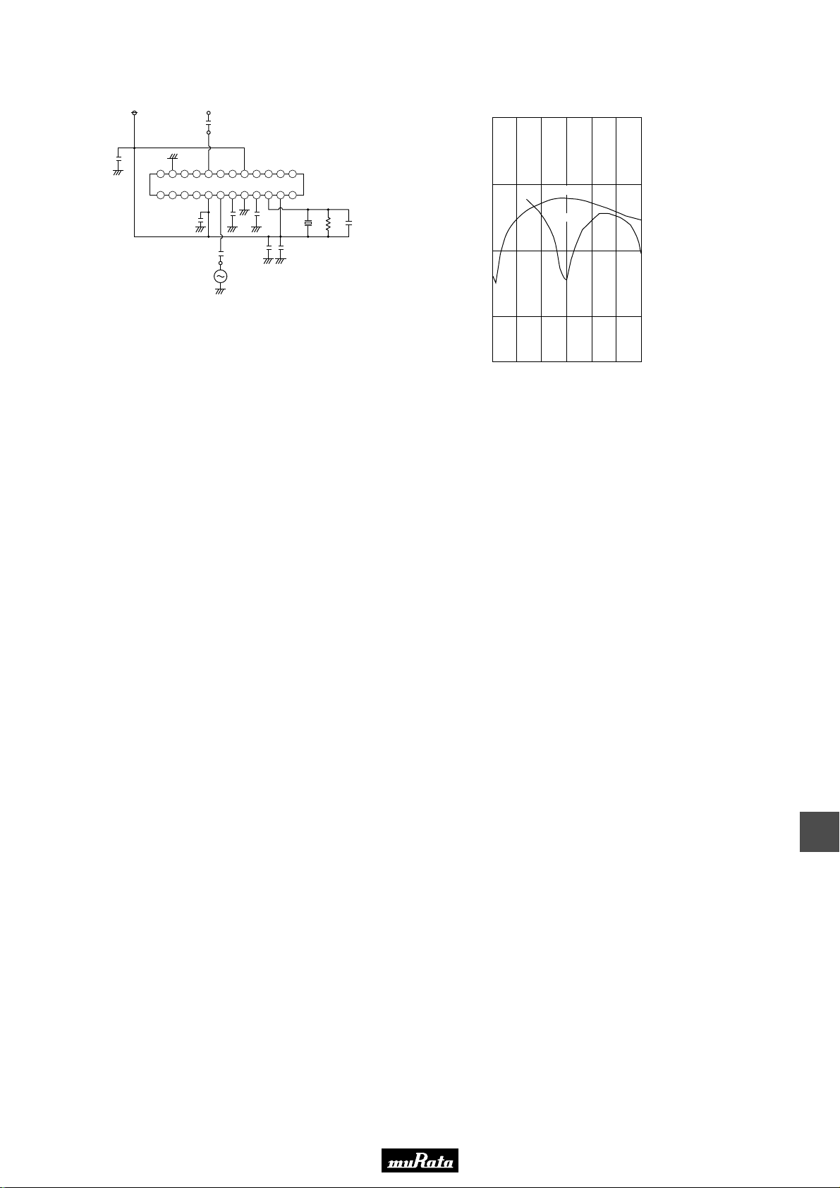
Please read CAUTION and Notice in this catalog for safety. This catalog has only typical specifications. Therefore you are requested
to approve our product specification or to transact the approval sheet for product specification, before your ordering.
P61E7.pdf 01.10.17
■ Test Circuit
0.01µF
222324
21 20
4 5 6 7 8 9321
0.01µF
0.01µF
S.S.G.
TA31272F
AF OUTVcc (5.0V)
0.01µF
19 18 17 16 15 14 13
10 11 12
0.01µF
1000pF
0.1µF
X R C
0.1µF
X: CDSCA10M7GF107-B0
R: 1.2 [kohm]
C: open
■ Frequency Characteristics
1000
100
10
Recovered AF Output Voltage (mV)
1
AF Output
Distortion
10.510.4 10.6 10.7 10.8 10.9 11.0
Frequency (MHz)
100
10
1
Distortion (%)
Input signal conditions
0.1
Input Level
Mod. Freq.
Freq.Dev.
100dBµ
1000Hz
±40kHz
43
12
Page 45
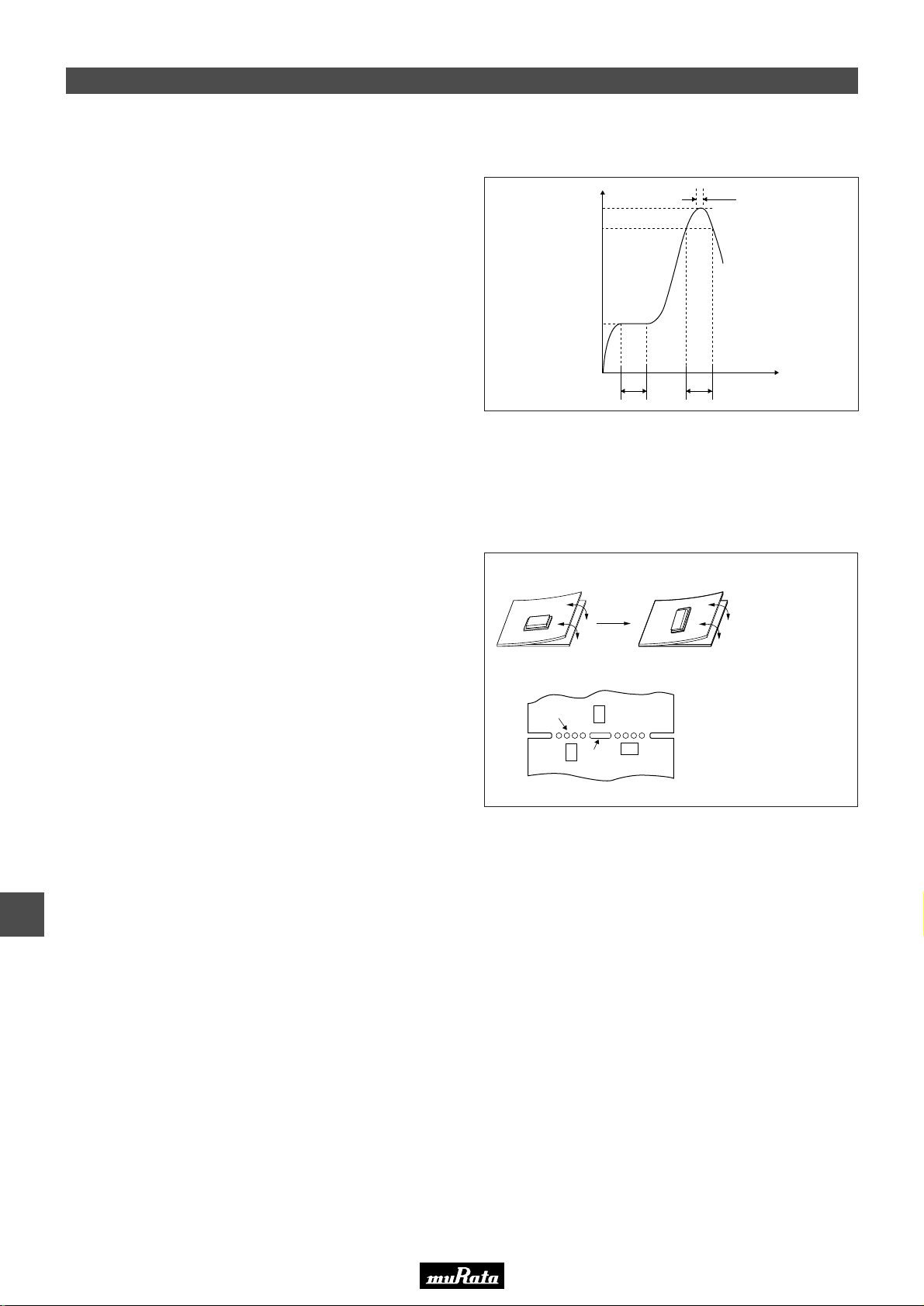
Please read CAUTION and Notice in this catalog for safety. This catalog has only typical specifications. Therefore you are requested
to approve our product specification or to transact the approval sheet for product specification, before your ordering.
Chip Type Discriminators CDSCA Series Notice
■ Notice (Soldering and Mounting)
1. Standard Reflow Soldering Condition
(1) Reflow
260
240
Temperature (°C)
150
(2) Soldering Iron
Lead terminal is directly contacted with the tip of
soldering iron of +280±5°C for 3.0 seconds±0.5 seconds.
6060
P61E7.pdf 01.10.17
5 sec
Gradual
Cooling
Time (sec.)
12
2. Wash
The component cannot be withstand washing.
■ Notice (Handling)
1. The component mounted on the PCB may be damaged if
excess mechanical stress is applied.
2. Layout the components on the PCB to minimize the
stress imposed by the warp or flexure of the board.
3. After installing components, if solder is excessively
applied to the circuit board, mechanical stress will cause
destruction resistance characteristics to be lower. To
prevent this, be extremely careful in determining shape
and dimension before designing the circuit board diagram.
4. When the positioning claw or pick up nozzle are worn, the
excess load is applied to the components while
positioning or placing are performed. Careful checking
and maintenance are necessary to prevent unexpected
trouble.
5. When correcting component's position with a soldering
iron, the tip of the soldering iron should not directly touch
the chip component. Depending on the soldering
conditions, the effective area of terminations may be
reduced. The use of solder containing Ag should be
considerd to prevent the electrode erosion.
6. Do not clean or wash the component as it is not
hermetically sealed.
7. In case of overcoating the part, coating conditions such
as material, curing temperature, and so on must be
evaluated deeply.
8. Accurate test circuit values are required to measure
electrical characteristics.
It may be a cause of mis-correlation if there is any
deviation, especially stray capacitance, from the test
circuit in the specification.
[Component direction]
[Component layout close to board]
Perforation
B
A
C
Slit
Put the
component
laterally to the
direction in
which stress
acts.
Susceptibility to
stress is in the order
of : A>C>B
44
Page 46
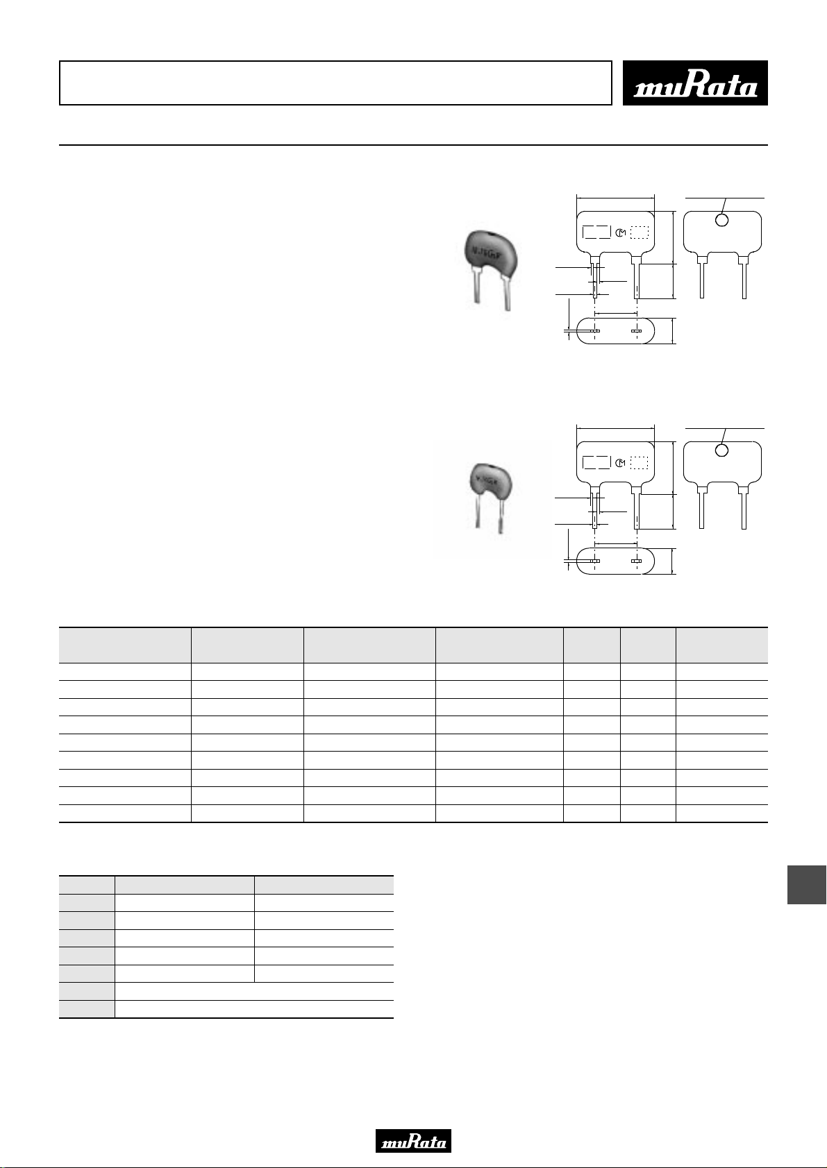
Please read CAUTION and Notice in this catalog for safety. This catalog has only typical specifications. Therefore you are requested
to approve our product specification or to transact the approval sheet for product specification, before your ordering.
Ceramic Filters (CERAFILr) for FM Receivers
Discriminators CDALA Series
P61E7.pdf 01.10.17
CDALA10M7 series forms a resonator on a piezoelectric
ceramic substrate. In combination with ICs, this type
obtains stable demodulation characteristics in wide
bandwidths.
■ Features
1. Compact and excellent mechanical strength.
2. Can be combined with various ICs. The IC is
determined by the last number in the part number.
3. Stable demodulation characteristics can be obtained
without adjustment.
4. The MG type for wide bandwidths and the MC type for
narrow bandwidths are available.
5. Stable temperature characteristics.
6. We recommend combination : ceramic discriminator
CDALA10M7 series and "CERAFIL" SFELA10M7 of the
same frequency rank.
CDALA10M7G_ Series
CDALA10M7C_ Series
0.4±0.1
0.5±0.1
0.3±0.1
0.4±0.1
0.5±0.1
0.3±0.1
M A R K I N G
M A R K I N G
8.0±1.0
0.65±0.1
5.0±0.2
8.0±1.0
0.65±0.1
5.0±0.2
E I A J
C O D E
E I A J
C O D E
Freq. Rank (Color Dot)
5.0±1.0
5.0±1.0
3.0±1.0
Freq. Rank (Color Dot)
5.0±1.0
5.0±1.0
3.0±1.0
(in mm)
(in mm)
Part Number
Center Frequency (fo)
(MHz)
Recovered Audio 3dB BW
(kHz)
Recovered Audio Output
(mV)
Distortion
(%)
IC Detection Method
CDALA10M7GA001-B0 10.700 ±30kHz 345 min. 25 min. 0.6 max. CX20029 Quadrature
CDALA10M7GA016-B0 10.700 ±30kHz 300 min. within60 to 90mV 0.9 max. TA8122F Quadrature
CDALA10M7GA018-B0 10.700 ±30kHz 300 min. 60 min. 0.9 max. TA8132N Quadrature
CDALA10M7GA046-B0 10.700 ±30kHz 330 min. 280 min. 1.0 max. LA1832 Quadrature
CDALA10M7GA048-B0 10.700 ±30kHz 400 min. 700 min. 1.0 max. LA1835 Quadrature
CDALA10M7GA092-B0 10.700 ±30kHz 300 min. 60 min. 1.0 max. TA2132P Quadrature
CDALA10M7CA001-B0 10.700 ±30kHz 242 min. 35 min. - CX20091 Quadrature
CDALA10M7CA005A-B0 10.700 ±30kHz 100 min. 600 min. 6.0 max. LA7770 Quadrature
CDALA10M7CA040-B0 10.700 ±30kHz 130 min. 40 min. 0.7 max. TEA5710 Quadrature
■ Center Frequency Rank Code
CODE
D
B
A
C
E
Z
M
30kHz Step
10.64MHz±30kHz
10.67MHz±30kHz
10.70MHz±30kHz
10.73MHz±30kHz
10.76MHz±30kHz
Combination A,B,C,D,E
Combination A,B,C
25kHz Step
10.650MHz±25kHz
10.675MHz±25kHz
10.700MHz±25kHz
10.725MHz±25kHz
10.750MHz±25kHz
13
45
Page 47
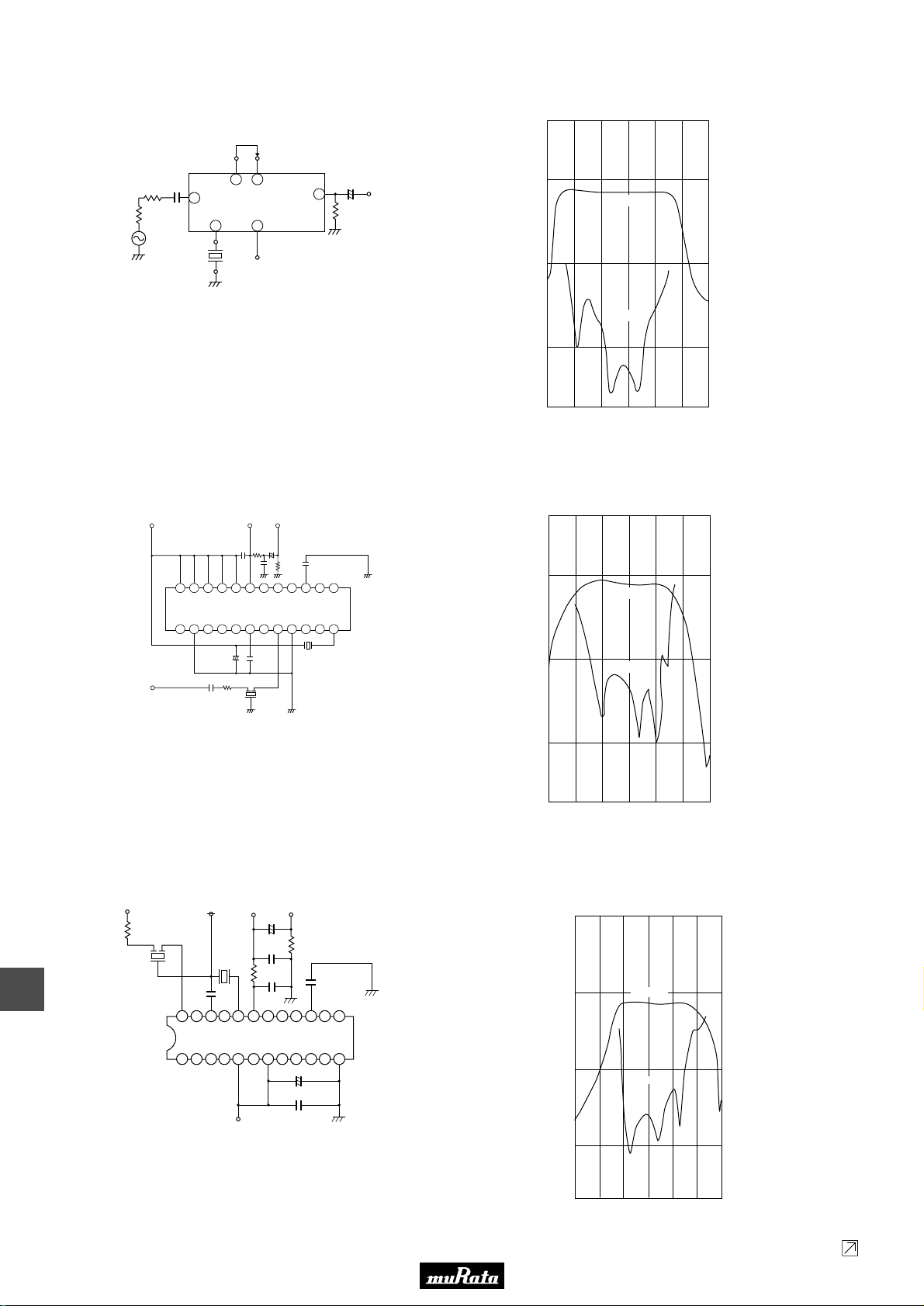
Please read CAUTION and Notice in this catalog for safety. This catalog has only typical specifications. Therefore you are requested
to approve our product specification or to transact the approval sheet for product specification, before your ordering.
■ CDALA10M7GA001-B0
Test Circuit
500
AFC
REF
0.01µ
280
Fg=50
5 33
39
CX20029
289
1µ
+ –
100k
AF OUTPUT
32
100
Frequency Characteristics
AF Output
P61E7.pdf 01.10.17
10
S.S.G.
CDALA10M7GA001
■ CDALA10M7GA016-B0
Test Circuit
VCC +3V DC Out AF Out
24 23 22 21 20 19 18 17 16 15 14 13
TA8122F (TOSHIBA)
1 2 3 4 5 6 7 8 9 10 11 12
22µ
IF in
SFELA10M7DF00
270
0.022µ
Vcc=+3.0V
1k
330p
+
2.5µ
+
0.033µ
0.022µ
24k
0.1µ
CDACV10M7GA016
Unit
R : Ω
C : F
Unit
R : Ω
C : F
10
Recovered AF Output Voltage (mV)
1
Distortion
10.610.5 10.7 10.8 10.9 11.010.4
Frequency (MHz)
1
Distortion (%)
0.1
Input signal conditions
Input Level
Mod. Freq.
Freq.Dev.
110dBµ
400Hz
±22.5kHz
Frequency Characteristics
500
100
AF Output
10
Recovered AF Output Voltage (mV)
1
Distortion
10.610.5 10.7 10.8 10.9 11.010.4
Frequency (MHz)
10
1
Distortion (%)
0.1
Input signal conditions
Input Level
Mod. Freq.
Freq.Dev.
80dBµ
1000Hz
±22.5kHz
13
■ CDALA10M7GA018-B0
Test Circuit
Vcc 3V
0.022µ
24 23 22 21 20 19 18 17 16 15 14 13
TA8132N (TOSHIBA)
1 2 3 4 5 6 7 8 9 10 11 12
Vcc 3V
46
1F in
270
SFELA10M7DF00
DC out AF out
2.2µ
+
0.033µ
CDALA10M7GA018
1k
330p
22µ
+
0.022µ
Frequency Characteristics
1000
24k
0.1µ
Unit
R : Ω
C : F
100
10
Recovered AF Output Voltage ( mV )
1
10.4 10.5 10.6 10.7 10.8 10.9 11.0
AF Output
Distortion
Frequency ( MHz )
100
10
1
Distortion (%)
0.1
Input signal conditions
Input Level 80 dBµ
Mod. Freq. 1000 Hz
Freq. Dev. ±22.5 kHz
Continued on the following page.
Page 48
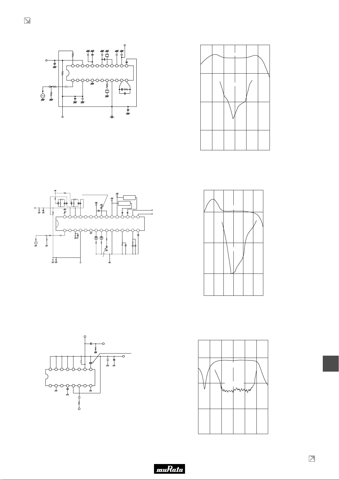
Please read CAUTION and Notice in this catalog for safety. This catalog has only typical specifications. Therefore you are requested
to approve our product specification or to transact the approval sheet for product specification, before your ordering.
Continued from the preceding page.
■ CDALA10M7GA046-B0
IF-IN
AFC
3.3µ
300
Test Circuit
CSBLA456KE2ZF15
1200p
0.047µ5.6k
+
+
75
24 1314151617181920212223
6.8k
1 12111098765432
0.047µ
10µ
REG
22µ
LA1832 (SANYO)
270
CDALA10M7GA046
+
0.047µ
+
1µ
Vcc (5V)
2.2µ
0.01µ
AF OUT
+
3k
1µ
0.01µ
1µ
+
100µ
Unit
R : Ω
C : F
1000
100
10
Recovered AF Output Voltage ( mV )
Frequency Characteristics
AF Output
Distortion
P61E7.pdf 01.10.17
100
10
1
Distortion ( % )
■ CDALA10M7GA048-B0
Test Circuit
CSBLA456KE2ZF15
1 2 3 4 5 6 7 8 9 10 11 12 13 14 15
+
0.047µ
10µ
CDALA10M7GA048
REG.
AFC
IF-IN
47n
3.3µ
Vt
+
5k
15k
30 29 28 27 26 25 24 23 22 21 20 19 18 17 16
300
0.047µ
75
47n
10µ
1500p
33n
+
1µ
LA1835 (SANYO)
1k 1k
VCC(7V)
10.9 11.0
0.1
Input signal conditions
Input Level 112 dBµ
Mod. Freq. 1000 Hz
Freq. Dev. ±75 kHz
1
10.510.4 10.6 10.7
Frequency ( MHz )
10.8
Frequency Characteristics
33n
L. P. F.
L. P. F.
1µ
0.47µ
Rch
Lch
Unit
R : Ω
C : F
10µ
10µ
++
510
20k
3k
+
+ +
10µ
500
100
10
Recovered AF Output Voltage (mV)
1
AF Output
Distortion
10.610.5 10.7 10.8 10.9 11.010.4
Frequency (MHz)
10
1
Distortion (%)
0.1
Input signal conditions
Input Level
Mod. Freq.
Freq.Dev.
112dBµ
1000Hz
±75kHz
■ CDALA10M7GA092-B0
Test Circuit
DC OUT
330p
1611521431341251161079
TA2132P(TOSHIBA)
+
4.7µ
270 0.01µ
IF-IN
2.2µ
+
20k
CDALA10M7GZ092-B0
8
AF OUT
0.033µ
Frequency Characteristics
500
Vcc(3.0V)
+
4.7µ
Unit
R : Ω
C : F
100
AF Output
10
Recovered AF Output Voltage (mV)
1
10.510.4 10.6 10.7 10.8 10.9 11.0
Distortion
Frequency (MHz)
10
13
1
Distortion (%)
0.1
Input signal conditions
Input Level 80dBµ
Mod.Freq. 1000Hz
Freq.Dev. ±22.5kHz
Continued on the following page.
47
Page 49
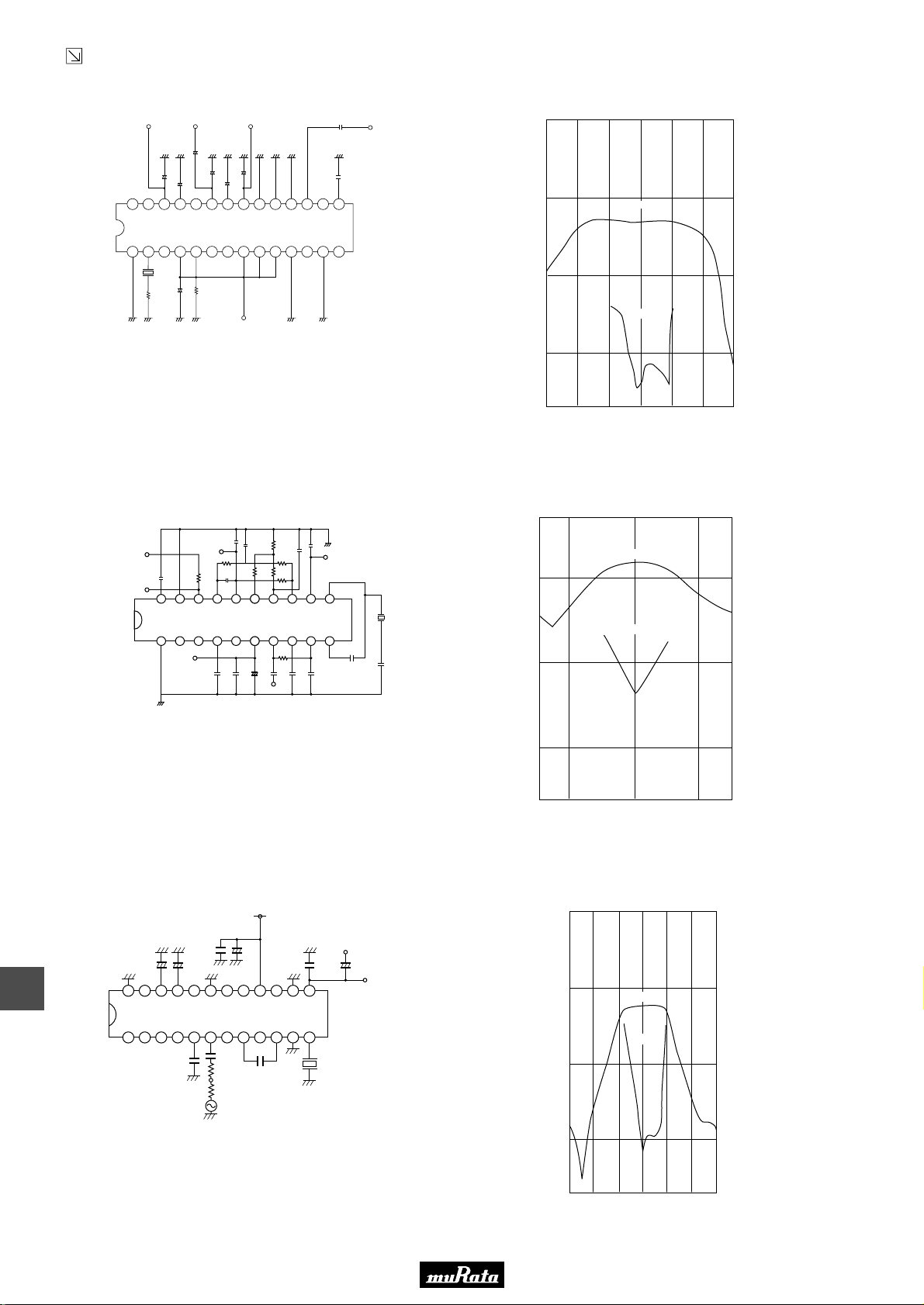
Please read CAUTION and Notice in this catalog for safety. This catalog has only typical specifications. Therefore you are requested
to approve our product specification or to transact the approval sheet for product specification, before your ordering.
Continued from the preceding page.
■ CDALA10M7CA001-B0
Test Circuit
VCC 5V AF Output AFC
33µ
0.1µ
4.7µ
+
100µ
+
10µ
+
28 27 26 25 24 23 22 21 20 19 18 17 16 15
1 2 3 4 5 6 7 8 9 10 11 12 13 14
+
10µ
100
CDALA10M7CA001
+
10µ
+
CX20090 (SONY)
1k
Ref.
0.01µ
IF in
0.01µ
Unit
R : Ω
C : F
1000
100
10
Recovered AF Output Voltage ( mV )
Frequency Characteristics
AF Output
Distortion
P61E7.pdf 01.10.17
100
10
1
Distortion ( % )
■ CDALA10M7CA005A-B0
Test Circuit
DC Bias
DC Bias
+5V
DATA OUT
0.01µ
20 19 18 17 16 15 14 13 12 11
1 2 3 4 5 6 7 8 9 10
Vcc=12V
470p
+5.2V
2k
5.6k
220p
IC : LA7770 (SANYO)
1000p
0.022p
1
10.510.4 10.6 10.7 10.8 10.9 11.0
Frequency ( MHz )
0.1
Input signal conditions
Input Level 110 dBµ
Mod. Freq. 400 Hz
Freq. Dev. ±22.5 kHz
Frequency Characteristics
5000
2k
0.1µ
20k
+
33µ
-
0.01µ
IF IN
470p
0.1µ
10k
10k
10k
50
Demod.OUT
1000
5p
CDALA10M7CA005A
0.01µ
0.01µ
0.01µ
Unit
R : Ω
C : F
100
Recovered AF Output Voltage ( mV )
10
10.6 10.7 10.8
AF Output
Distortion
Frequency ( MHz )
500
100
10
Distortion ( % )
1
Input signal conditions
Input Level 100 dBµ
Mod. Freq. 1000 Hz
Freq. Dev. ±75 kHz
13
■ CDALA10M7CA040-B0
Test Circuit
+
100µ
24 23 22 21 20 19 18 17 16 15 14 13
1 2 3 4 5 6 7 8 9 10 11 12
48
0.01µ
10µ
+ +
TEA5710 (PHILIPS)
0.22µ
0.01µ
280
50
S.S.G.
VCC (3V)
100µ
0.22µ
0.01µ
AF-OUT
+
1µ
DC-OUT
Unit
R : Ω
C : F
Frequency Characteristics
1000
100
10
Recovered AF Output Voltage ( mV )
1
10.4 11.0
AF Output
Distortion
10.5 10.6 10.7 10.8 10.9
Frequency ( MHz )
100
10
1
Distortion (%)
0.1
Input signal conditions
Input Level 100 dBµ
Mod. Freq. 1000 Hz
Freq. Dev. ±22.5 kHz
Page 50
Please read CAUTION and Notice in this catalog for safety. This catalog has only typical specifications. Therefore you are requested
to approve our product specification or to transact the approval sheet for product specification, before your ordering.
Lead Type Discriminators Notice
■ Notice (Soldering and Mounting)
The component cannot be withstand washing.
■ Notice (Handling)
1. Do not use this product with bend. The component
may be damaged if excess mechanical stress is
applied to it mounted on the printed circuit board.
2. The component may be damaged when an excess stress
will be applied.
3. All kinds of re-flow soldering must not be applied
on the component.
4. Do not clean or wash the component as it is not
hermetically sealed.
5. Do not use strong acidity flux, more than 0.2wt%
chlorine content, in flow soldering.
6. In case of covering discriminator with over coat,
conditions such as material of resin, cure
temperature, and so on should be evaluated well.
7. Accurate test circuit values are required to
measure electrical characteristics. It may be a
cause of mis-correlation if there is any deviation,
especially stray capacitance, from the test
circuit in the specification.
P61E7.pdf 01.10.17
49
13
Page 51
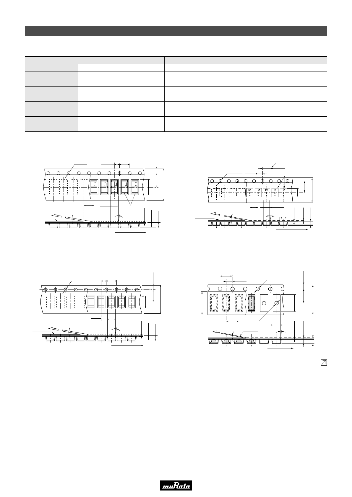
Please read CAUTION and Notice in this catalog for safety. This catalog has only typical specifications. Therefore you are requested
to approve our product specification or to transact the approval sheet for product specification, before your ordering.
Packaging
■ Minimum Quantity
Part Number Taping ø180mm
SFECV
SFECS
SFELA
SFELB
SFVLA
SFKLA
SFTLA
CDACV / CDSCA
CDALA
2,000
2,000
2,000
Ammo Pack
1,500
1,500
1,000
1,500
1,500
P61E7.pdf 01.10.17
Bulk
500
500
500
500
500
500
■ Chip Type CERAFILr
SFECV Series
W0.1
φ1.5
Y0.0
∗∗∗∗∗∗∗∗∗∗∗∗∗
Peeling strengh (0.1Y0.7N)
Cover Tape
Part number marked side is always facing upside.
The feeding holes side of cavity tape is always input terminal.
10 max.
4.0T0.1
■ Chip Type Discriminator
CDACV Series
W0.1
W0.1
2.0T0.05 4.0T0.1
2.0T0.05 4.0T0.1
φ1.5
φ1.5
Y0.0
Y0.0
Peeling strengh (0.1Y0.7N)
Cover Tape
10 max.
4.0T0.1
2.0T0.05 4.0T0.1
3.0T0.1
3 max.
User Direction of Feed
3.0T0.1
3 max.
Chip Filter
■ Small Chip Type CERAFILr
SFECS Series
φ1.55T0.05
2.0T0.05
5.5T0.05 1.75T0.1
-0.2
7.3T0.01
+0.08
12.0
Peeling strength
0.1~0.7N
W0.1
Y0.05
1.9T0.1
1.7
Cover film
· Part Number marked side is always facing upside.
· The feeding holes side of cavity tape is always input terminal.
10˚ max.
4.0T0.1
3.35T0.1
3˚max.
∗∗
0.3T0.05
40T0.15
10 pitch accumulated
4.0T0.1
Chip Filter
3.45
0.3T0.05
User direction of feed
4.3
0.05
(in mm)
5.5T0.05
2.02T0.1
12.0T0.2
■ Chip Type Low-Profile Type Discriminator
CDSCA Series
0.3T0.05
3.8T0.1
0.3T0.01
4.0±0.1
4.0±0.1
2.0±0.05
10˚
+0.1
Ø1.5
Cover Film
1.75T0.1
5.5T0.5 1.75T0.1
12.0T0.2
12.0T0.2
W0.1
Y0.05
1.9T0.1
1.7
(9.5)
The cover film peel
strength force 0.1~0.7N
-0
2.2±0.1
Ø1.5
+0.1
-0
5.5±0.05 1.75±0.1
3˚max.
4.7±0.1
0.3±0.05
1.25±0.05
12.0±0.2
(1.85max.)
13
Part number marked side is always facing upside. User Direction of Feed
50
Direction of FeedPart Number marked side is always facing upside
(in mm)
Continued on the following page.
Page 52
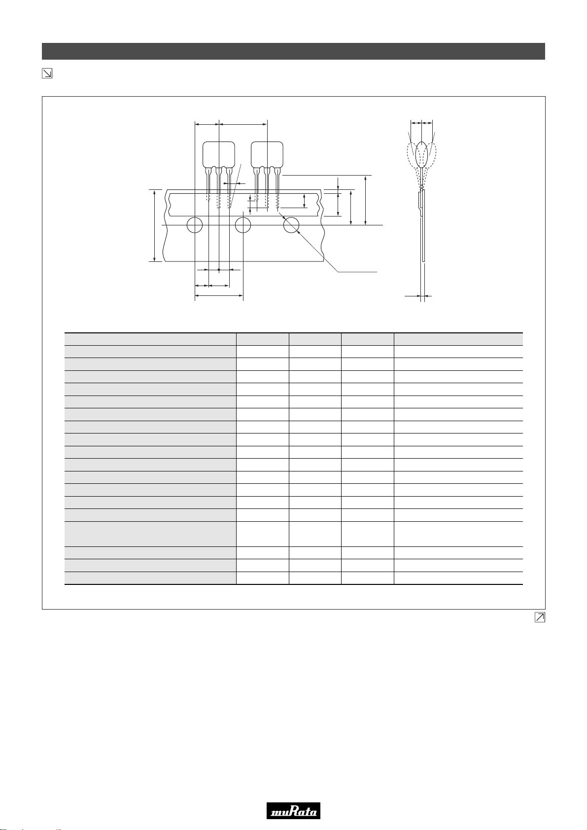
Please read CAUTION and Notice in this catalog for safety. This catalog has only typical specifications. Therefore you are requested
to approve our product specification or to transact the approval sheet for product specification, before your ordering.
Continued from the preceding page.
■ Lead Type CERAFILr SF_LA Series
P61E7.pdf 01.10.17
Packaging
P2 P
W
F
1 F1
1
F
P
P0
Item Code Dimensions Tolerance Remarks
Lead Length under the Hold Down Tape
Length of Cat off
Pitch of Components
Pitch of Sprocket Hole (1)
Length from Hole Center to Lead
Length from Hole Center to Component Center
Pitch of the Terminal (1)
Pitch of the Terminal (2)
Slant to the Forward or Backward
Slant to the Left or Right
Width of Carrier Tape
Width of Hold Down Tape
Position of Sprocket Hole
Gap of Hold Down Tape and Carrier Tape
Distance Between the Center of Sprocket
Hole and Lead Stpper
Diameter of Sprocket Hole
Total Tape Thickness
Pitch of Sprocket Hole (2)
∆S
∆h ∆h
1
W2
1
L2
L1
L2
P
P0
P1
P2
F
F1
∆h
∆S1
W
W0
W1
W2
H0
D0
t
P020
L
3.0 min.
2.0 max.
12.7
12.7
3.85
6.35
5.0
2.5
0
0
18.0
6.0 min.
9.0
0
18.0
ø4.0
0.6
254.0
H0
W0
W1
D0
t
To distinguish the direction
±0.5
±0.2
±0.5
±0.5
+0.5
–0.2
±0.2
±1.0
±1.0
±0.5
Must not protrude to the carrier tape
±0.5
+0.5
–0
±0.5
±0.2
±0.2
±1.5
The pitch of 20 sprocket holes
(in mm)
Continued on the following page.
13
51
Page 53
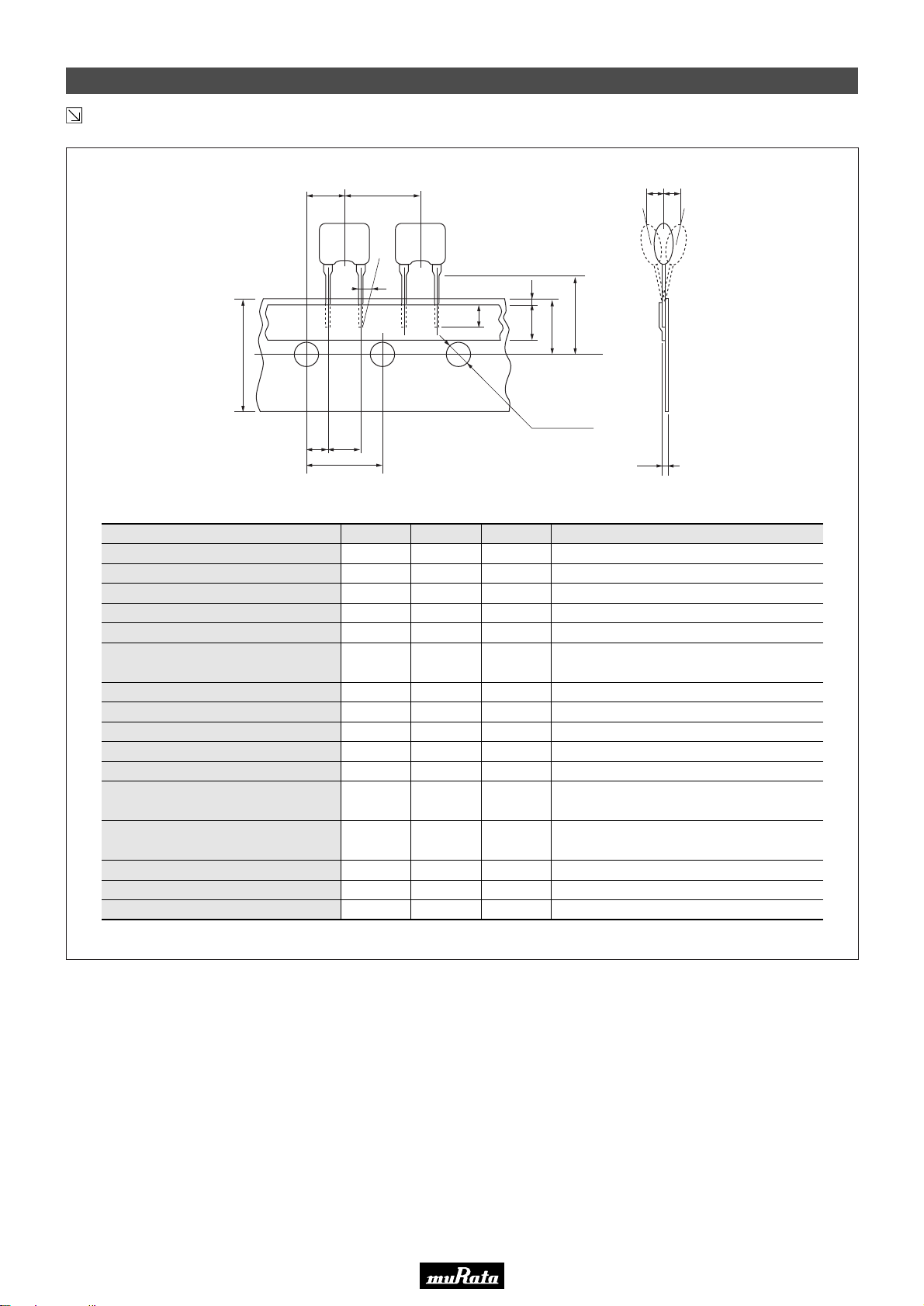
Please read CAUTION and Notice in this catalog for safety. This catalog has only typical specifications. Therefore you are requested
to approve our product specification or to transact the approval sheet for product specification, before your ordering.
Packaging
Continued from the preceding page.
■ Lead Type Discriminator CDALA Series
P61E7.pdf 01.10.17
W
P
Item Code Dimensions Tolerance Remarks
Lead length under the hole down tape
Pitch of component
Pitch of sprocket hole (1)
Length from hole center to lead
Length from hole center to component center
Lead spacing
Slant to the forward or backward
Slant to the left or right
Width of carrier tape
Width of hold down tape
Position of sprocket hole
Gap of hold down tape and
Carrier tape
Distance between the center of
sprocket hole and lead stopper
Diameter of sprocket hole
Total tape thickness
Pitch of sprocket hole (2)
P2 P
1
F
P0
∆S
Po20
∆S
L
P
P
P1
P2
F
∆h
W
W
W1
W2
H0
D0
∆h ∆h
1
W2
1
L
1
0
0
t
3.0 min.
12.7
12.7
3.85
6.35
5.0
0
1
0
18.0
6.0 min.
9.0
0
18.0
ø4.0
0.6
254.0
———
±0.5
±0.2
±0.5
±0.5
+0.5
-0.2
±1.0
±1.0
±0.5
———
±0.5
+0.5
-0.0
±0.5
±0.2
±0.2
±1.5
H0
W0
W1
D0
t
Hold down tape doesn't exceed the carrier tape
The pitch of 20 sprocket holes
(in mm)
13
52
Page 54
Please read CAUTION and Notice in this catalog for safety. This catalog has only typical specifications. Therefore you are requested
CDALA10M7GA001
CDALA10M7GA002
CDALA10M7GA004
CDALA10M7GA005
CDALA10M7GA006
CDALA10M7GA007
CDALA10M7GA008
CDALA10M7GA009
CDALA10M7GA011
CDALA10M7GA012
CDALA10M7GA013
CDALA10M7GA014A
CDALA10M7GA015
CDALA10M7GA016
CDALA10M7GA017
CDALA10M7GA018
CDALA10M7GA019
CDALA10M7GA020
CDALA10M7GF021A
CDALA10M7GA022
CDALA10M7GA023
CDALA10M7GF024
CDALA10M7GA025
CDALA10M7GA026
CDALA10M7GA027
CDALA10M7GA027N
CDALA10M7GA028
CDALA10M7GA029
CDALA10M7GA030
CDALA10M7GA031
CDALA10M7GA032
CDALA10M7GA033
CDALA10M7GA034V
CDALA10M7GA035
CDALA10M7GA036
CDALA10M7GA037
CDALA10M7GA038
CDALA10M7GA039
CDALA10M7GA040
CDALA10M7GA041
CDALA10M7GA042
CDALA10M7GA043
CDALA10M7GA044
CDALA10M7GA045
CDALA10M7GA046
CDALA10M7GA047
CDALA10M7GA048
CDALA10M7GA049
CDALA10M7GA050
CDALA10M7GA051
CDALA10M7GA052
CDALA10M7GA053
CDALA10M7GA054
CDALA10M7GA055
CDALA10M7GA056
CDALA10M7GA057
CDALA10M7GA058
CDALA10M7GA059
CDALA10M7GA060
CDALA10M7GA061
Part Number IC Manufacturer IC
Sony
Sony
Rohm
Rohm
Toshiba
Sanyo
Toshiba
Toshiba
Panasonic
Sony
Panasonic
Panasonic
Sanyo
Toshiba
Philips
Toshiba
Rohm
Philips
Philips
Sanyo
Sanyo
Philips
Telefunken
Sanyo
Sony
Sony
Telefunken
Philips
Philips
Toshiba
Sony
Toshiba
Telefunken
Philips
Toshiba
Sanyo
Siemens
Toshiba
Philips
Rohm
Philips
Sanyo
Siemens
Toshiba
Sanyo
Philips
Sanyo
Motorola
Toshiba
Siemens
Motorola
Panasonic
Sony
Philips
NEC
Toshiba
Toshiba
Samsung
Rohm
Philips
CX20029
CX20076
BA4234L
BA4230AF
TA7640AP
LA1260
TA7303P
TA7130P
AN7004
CXA1030P
AN7007SU
AN7006S
LA1816
TA8122AN/F
TEA5591
TA8132AN/AF
BA1440
NE604
TBA229-2
LA1810
LA7770
TDA2557
U829B
LA1805
CXA1238
CXA1238N
U2501B
TBA120U
TEA5592
TA2003
CXA1343M
TA2007N
U4490B
TEA5594
TA2029
LA1830
TDA6160X
TA8186
TEA5710
BA4220
SA605
LA1831
TDA6160-2X
TA2008A/AN
LA1832/M
SA626
LA1835/M
MC13156
TA2022
TDA1576T
MC13173
AN7232
CXA1376AM
TEA5712T
µPC1391M
TA2057
TA2046
KA2244
BA1448
TEA5762/5757
CDALA10M7GF062
CDALA10M7GA063
CDALA10M7GA064
CDALA10M7GA065
CDALA10M7GA066
CDALA10M7GA067
CDALA10M7GA068
CDALA10M7GA069
CDALA10M7GA070
CDALA10M7GA071
CDALA10M7GF072
CDALA10M7GA073
CDALA10M7GA075
CDALA10M7GA076
CDALA10M7GA077
CDALA10M7GA078
CDALA10M7GA079
CDALA10M7GA080
CDALA10M7GA080A
CDALA10M7GA081
CDALA10M7GA082
CDALA10M7GA083
CDALA10M7GA084
CDALA10M7GA085
CDALA10M7GA086
CDALA10M7GA087
CDALA10M7GA088
CDALA10M7GA089
CDALA10M7GA090
CDALA10M7GA091
CDALA10M7GA092
CDALA10M7GA092D
CDALA10M7GA093
CDALA10M7GA094
CDALA10M7GA095
CDALA10M7GA096
CDALA10M7GA097
CDALA10M7GA098
CDALA10M7GA100
CDALA10M7GA100A
CDALA10M7GA101
CDALA10M7GA102
CDALA10M7GA103
CDALA10M7GA104
CDALA10M7GA105A
CDALA10M7GA106
CDALA10M7GF107
CDALA10M7GF108A
CDALA10M7GF109
CDALA10M7GA110
CDALA10M7CA001
CDALA10M7CA002
CDALA10M7CA004A
CDALA10M7CA005A
CDALA10M7CA006
CDALA10M7CA009
CDALA10M7CA040
Part Number IC Manufacturer IC
Part Number IC Manufacturer
Toko
Samsung
Samsung
Samsung
Rohm
Rohm
Sony
Sony
Sanyo
Toshiba
Toshiba
Motorola
Sony
Sony
Toshiba
Sony
Sanyo
Toshiba
Toshiba
Telefunken
Toshiba
Sanyo
Rohm
Philips
Sanyo
Motorola
Toshiba
Samsung
Samsung
Samsung
Toshiba
Toshiba
Sony
Sanyo
Temic
Philips
Matsushita
Philips
Toshiba
Toshiba
Sanyo
Toshiba
Samsung
Rfmd
Philips
Fujitsu
Toshiba
Sanyo
Toko
Dspg
Sony
Toshiba
Motorola
Sanyo
Philips
Toshiba
Philips
TK14581
KA2292
KA2295
KA2298
BA4110
BA4240L
CXA1991N
CXA1538M/N/S
LA1150
TA7765
TA31161
MC13158
CXA1611
CXA3067M
TA2111
CX1691M
LA1838/M
TA2104AFN
TA2104F
U4313B
TA2099N
LA1827
BH4126FV
SA639
LA1833
MC3363
TA8721ASN
KA22425
KA22901
KA2297
TA2132
TA2132BP
CXA1111
LA1822
U2765B
SA636DK
AN6138SH
CAA3220TS
TA2149N
TA2149AN
LA1823
TA2142FN
KB22902
RF2925
TEA5757HL
MB15G611
TA31272FN
LA1225M
TK14588
DS9RF21
CX20091
TA7687P/F
MC3356P
LA7770
TEA5591
TA7640AP
TEA5710
IC
to approve our product specification or to transact the approval sheet for product specification, before your ordering.
Test Circuit of Ceramic Discriminator
P61E7.pdf 01.10.17
13
53
Page 55
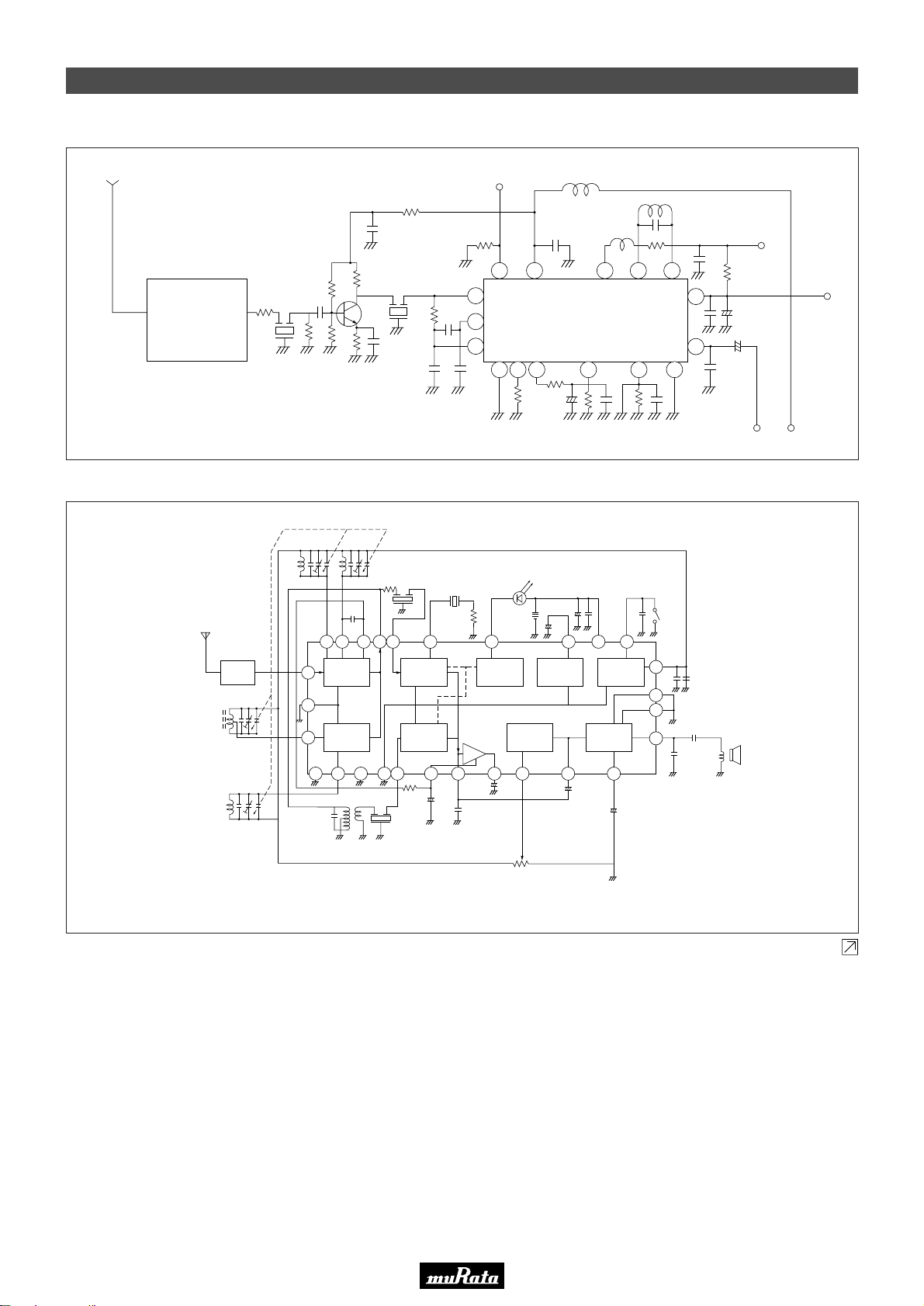
Please read CAUTION and Notice in this catalog for safety. This catalog has only typical specifications. Therefore you are requested
to approve our product specification or to transact the approval sheet for product specification, before your ordering.
Example of Appllied Circuit
■ LA1140(Automotive Radio)
P61E7.pdf 01.10.17
FRONT
END
■ CXA1019M(Radio)
FM
BPF
AM ANT
AM OSC
SFELA10M7HAA0-B0
1
R
C1
100
0.022
C.F.
FM PF FM OSC
12
13
10
R4
10k
1.8k1.8k
R3R2
FM
FRONT
END
AM
FRONT
END
R6
330
R
2
1k
IF
OUT
R7 200
C3
0.047
SFELA10M7HAA0-B0
C.F.
0.047
8
R
C6
330
2
C
0.022
0.047 x 2
20 161811 5
FM IF
IN
FM IF
AMP
DETECTOR
AM IF
AMP
DETECTOR
AM IF
IN
®
2
FM DISCRI
W
FM CERAFIL
(SFELA10M7FA00-B0)
AGC
VR1
150k
16
12 9 11 13
1
2
3
C5C4
4 105 146
R9
220k
CERAMIC DISCRIMINATOR
(CDALA10M7CA001-B0)
R
1917678 14
METER
TUNING
METER
CXA1019M(SONY)
VOL
DEP
W
OUT
2.2µ
7
C
0.047
22k
R
W
RIPPLE
FILTER
L1 2.2µH
LA1140
(SANYO)
C14
0.047
10
+
R2
C15
47k
W
25 26 13
Vcc
REGULATOR
AF
PRE/POWER
AMP
AF IN
W
R14
C13
33p
FM/AM
BAND SELECT
REG
OUT
8
28
1
27
W
C8
0.047
7
8
W
C11
33p
Vref.
R
13
12k
+
9 0.047
C
10 4.7µ
C
+
SP
AFC
L2
15
R12
3244212322
W
13
54
AM CERAFIL
(SFULA455KU2B-B0)
®
VOL
No adjustment is needed the FM detection stage due to use the ceramic discriminator.
Continued on the following page.
Page 56
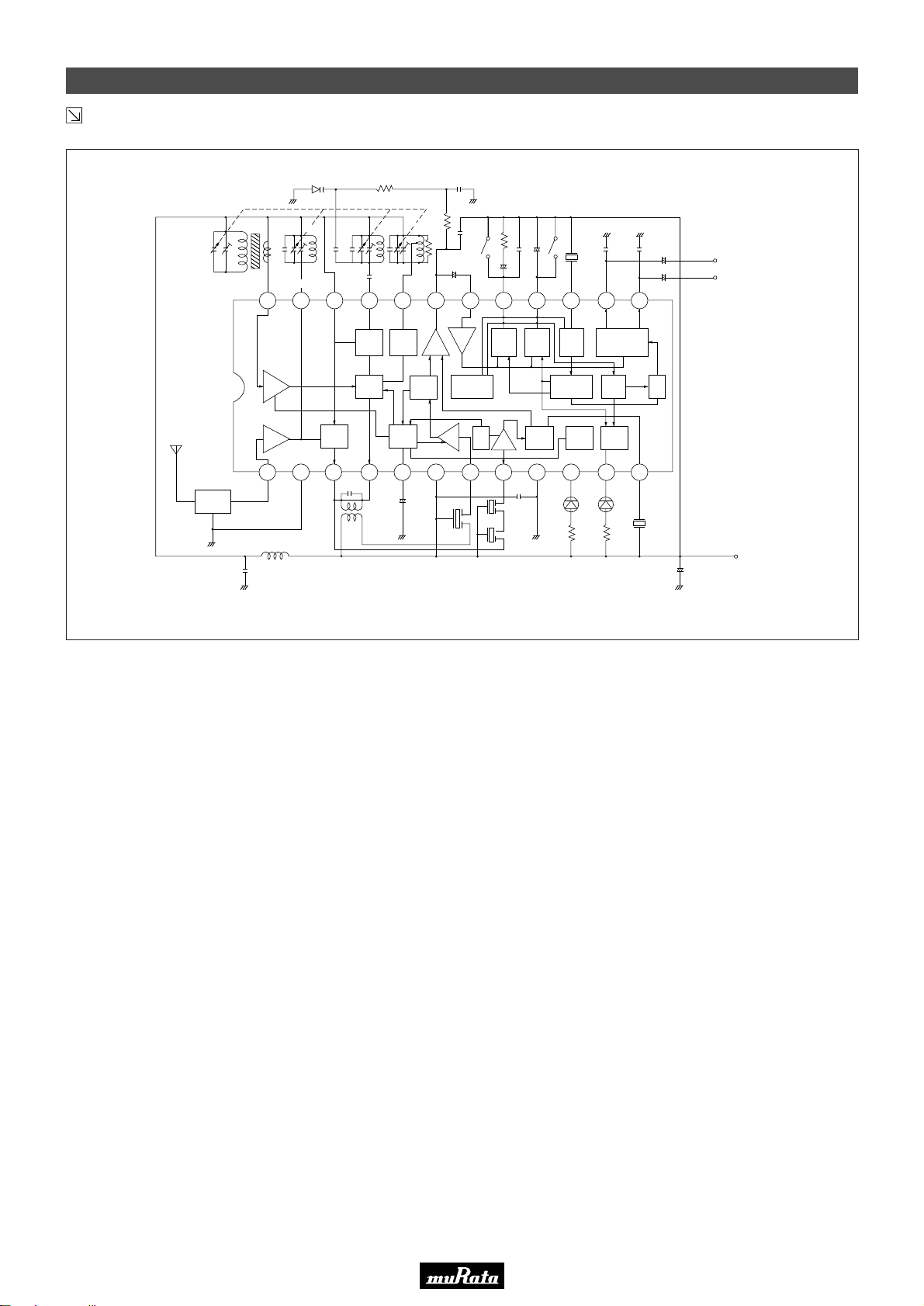
Please read CAUTION and Notice in this catalog for safety. This catalog has only typical specifications. Therefore you are requested
to approve our product specification or to transact the approval sheet for product specification, before your ordering.
Example of Appllied Circuit
Continued from the preceding page.
■ TA8122F(Radio)
P61E7.pdf 01.10.17
IS2236
100k
0.022µF
CSBLA456KE2ZF16-B0
BPF
100k
L3
AM
PF
FM
RF IN
0.022µ
L1 T1L2
20p
FM
PF
24 23 22 20 19 18 17 16 15 14 13
AM
RF
FM
RF
10µH
OUTINVcc1
FM
MIX
5p
FM
OSCAMOSC
AM
MIX
AM
MIX
22p
15p
21
FM
OSCAMOSC
AM
MIX
AM
AGC
T
2
8p
DEF
OUT
33k
10µF
AF
FM
DET
AM
AGC
654321 7 8 9 10 11 12
Vcc2GND1
W
33µ
330p
MO AM
W
MPX
LPF1
IN
PRE
AM/FM
MONO SW
AM
L
IF
DET
FM
AM
IF IN
IF IN
SFELA10M7FA00-B0SFULA455KU2B-B0
ST
22k
W
0.1µ
LPF2 VCO
Phase
COM
FM
IF
GND2
0.033µ
0.1µ
0.068µ
Phase
COM
FM
DET
FM
W
Freq
Divider
TUN
LED
VCO
TUN
LED
0.015µ
OUTLOUT
R
ST
DECODER
HYX SW
ST
LED
ST
QUAD
LED
560
560
CDALA
10M7GA16-B0
Detection and MPX stage adjustment ceramic discriminator and ceramic resonator (CERALOCK®)
4.7µ
0.015µ
W
W
4.7µ
L
R
TA8122F(TOSHIBA)
Vcc
W
22µ
(3V)
55
13
Page 57

Please read CAUTION and Notice in this catalog for safety. This catalog has only typical specifications. Therefore you are requested
to approve our product specification or to transact the approval sheet for product specification, before your ordering.
P61E7.pdf 01.10.17
Note:
1. Export Control
For customers outside Japan
<
Murata products should not be used or sold for use in the development, production, stockpiling or utilization of any conventional weapons or mass-destructive
weapons (nuclear weapons, chemical or biological weapons, or missiles), or any other weapons.
For customers in Japan
<
For products which are controlled items subject to the “Foreign Exchange and Foreign Trade Law” of Japan, the export license specified by the law is required
for export.
2. Please contact our sales representatives or product engineers before using our products listed in this catalog for the applications listed below which require
especially high reliability for the prevention of defects which might directly cause damage to the third party's life, body or property, or when intending to use one
of our products for other applications than specified in this catalog.
q Aircraft equipment
w Aerospace equipment
e Undersea equipment
r Power plant equipment
t Medical equipment
y Transportation equipment (vehicles, trains, ships, etc.)
u Traffic signal equipment
i Disaster prevention / crime prevention equipment
o Data-processing equipment
!0 Application of similar complexity and/or reliability requirements to the applications listed in the above
3. Product specifications in this catalog are as of May 2001. They are subject to change or our products in it may be discontinued without advance notice. Please
check with our sales representatives or product engineers before your ordering. If there are any questions, please contact our sales representatives or product
engineers.
4. Please read CAUTION and Notice in this catalog for safety. This catalog has only typical specifications. Therefore you are requested to approve our product
specification or to transact the approval sheet for product specification, before your ordering.
5. Please note that unless otherwise specified, we shall assume no responsibility whatsoever for any conflict or dispute that may occur in connection with the effect
of our and/or third party's intellectual property rights and other related rights in consideration of your using our products and/or information described or
contained in our catalogs. In this connection, no representation shall be made to the effect that any third parties are authorized to use the rights mentioned
above under licenses without our consent.
6. None of ozone depleting substances (ODS) under the Montreal Protocol is used in manufacturing process of us.
>
>
Head Office
2-26-10, Tenjin Nagaokakyo-shi, Kyoto 617-8555, Japan Phone:81-75-951-9111
http://www.murata.co.jp/products/
International Division
3-29-12, Shibuya, Shibuya-ku, Tokyo 150-0002, Japan
Phone:81-3-5469-6123 Fax:81-3-5469-6155 E-mail:[email protected]
 Loading...