

Page 1

Philips Semiconductors Product specification
NE/SE5562Switched-mode power supply control circuit
1
1994 Aug 31 853-0811 13721
DESCRIPTION
The NE/SE5562 is a single-output control circuit for switched-mode
power supplies. This single monolithic IC contains all control and
protection features needed for full-featured switched-mode power
supplies.
The 100mA source/sink output is designed to drive power FETs
directly. The associated output logic is designed to prevent double
pulsing or cross-conduction current spiking on the output.
All of the control and protect features work cycle-by-cycle up to the
maximum operating frequency of 600kHz.
For ease of interface, all digital inputs are TTL or CMOS compatible.
The NE5562 is supplied in 20-pin glass/ceramic (Cerdip), plastic
DIP, and plastic SO packages. The NE grade part is characterized
and guaranteed over the commercial ambient temperature range of
0°C to +70°C and junction temperature range of 0°C to +85°C. The
SE5562 is supplied in the glass/ceramic (Cerdip) package. The SE
grade part is characterized and guaranteed over the ambient
temperature range of -55 to +125°C and junction temperature range
of -55 to +135°C.
FEATURES
•Stabilized power supply
•Temperature-compensated reference source
•Sawtooth generator
•Pulse width modulator
•Remote on/off switching
•Current limiting (2 levels)
PIN CONFIGURATION
1
2
3
4
5
6
7
8
9
10
11
12
13
14
20
19
18
17
16
15
D, F, N Packages
TOP VIEW
FEED FORWARD
EXTERNAL MOD IN
DUTY CYCLE CONTROL
REMOTE ON/OFF
FEEDBACK VOLTAGE
ERROR AMP OUT
C
T
R
T
V
I
V
Z
GROUND
OUTPUT
DEMAG OVERVOLT IN
C DELAY
AUX COMP INPUT
CURRENT SENSE
OUT INVERT CONTROL
AUX COMP HYSTERESIS
V
S
EXTERNAL SYNC IN
SL00388
Figure 1. Pin Configuration
•Auxiliary comparator, with adjustable hysteresis
•Loop fault protection
•Demagnetization/overvoltage protection
•Duty cycle adjust and clamp
•Feed-forward control
•External synchronization
•Total shutdown after adjustable number of overcurrent faults
•Soft-start
ORDERING INFORMATION
DESCRIPTION TEMPERATURE RANGE ORDER CODE DWG #
20-Pin Plastic Small Outline (SO) Package 0 to +70°C NE5562D 1021B
20-Pin Plastic Dual In-Line Package (DIP) 0 to +70°C NE5562N SOT146-1
20-Pin Ceramic Dual In-Line Package (CERDIP) -55°C to +125°C SE5562F SOT146-1
Page 2
Philips Semiconductors Product specification
NE/SE5562Switched-mode power supply control circuit
1994 Aug 31
2
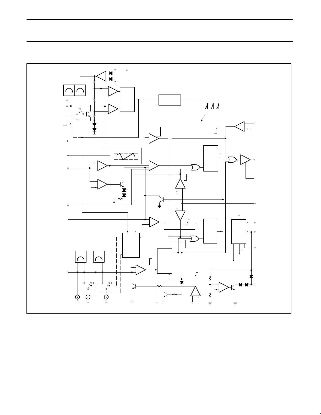
BLOCK DIAGRAM
FEEDFORWARD
1
11
EXTERNAL
SYNC IN
+
+
–
+
S
R
Q
OSC
LATCH
OSCILLATOR
3
2
OFF
ON
CLOCK
TIME
DELAY
OFF
ON
1.5V
REMOTE
ON/OFF
6
ERROR
AMP
OUT
10
FEEDBACK
VOLTAGE
8
EXTERNAL
MOD
IN
4
DUTY CYCLE
CONTROL
5
CLOCK
LOOP FAULT
COMP
0.955V
3.80V
PWM
COMP
ON/OFF
COMP
2k
OC1
0C2
0.955V
SLOW
START
COMP
OC2
NORM
–
+
0.528V
OVERCURRENT 1
COMP
OVERCURRENT 2
COMP
OC CHARGE PUMPS
NORM
LV STOP
START/
STOP
LATCH
R
S
Q
0.645V
OUTPUT
LATCH
OC1
NORM
LOW BULK
BULK
SENSE
COMP
1:1
1:1
16
POWER
SUPPLY
CKTS
3.80V
SHUT
DOWN
LATCH
3.80V
OC ACCUM
COMP
TRIP
NORM
S
R
Q
–
+
+V
+V
OC1 OC2
AUXILIARY
COMP
HYSTERESIS
AUXILIARY
COMP
INPUT
12
ERROR
AMP
DEMAG/OV
IN
18
3.80V
DEMAG/OV
COMP
0V
NORM
OUTPUT
19
OUTPUT
INVERT
CONTROL
15
POWR
OUTPUT
NOR
CURRENT
SENSE
GND
14
20
9
0.955V
0.528V
0.645V
DELAYED
CLOCK
S
R
–
+
–
+
–
+
+
–
–
–
–
+
–
+
–
+
13 3.80V
3.80V
–
+
–
+
C
DELAY
1µA
11µA 80µA
V
I
V
Z
V
S
17
Q
OC1-2
LATCHES
7
SL00389
Figure 2. Block Diagram
Page 3

Philips Semiconductors Product specification
NE/SE5562Switched-mode power supply control circuit
1994 Aug 31
3
ABSOLUTE MAXIMUM RATINGS
SYMBOL PARAMETER RATING UNIT
Supply
V
S
voltage-fed mode (Pin 17) 16 V
I
CC
current-fed mode (Pin 7) 30 mA
Output transistor 100 mA
output current
Sync (Pin 11) V
S
V
Duty cycle control (Pin 5) V
Z
V
Remote on/off (Pin 6) V
S
V
Output invert control (Pin 15) V
S
V
Feedback pin (Pin 8) V
Z
V
C
DELAY
(Pin 16) V
Z
V
External mod in (Pin 4) V
S
V
FF Feed-forward (Pin 1) V
S
V
Demag/overvoltage in (Pin 18) V
Z
V
Current sense (Pin 14) V
S
V
80Low supply sense and hysteresis
(Pins 12, 13)
V
S
V
T
J
Operating junction temperature 135 °C
T
STG
Storage temperature range -65 to +150 °C
T
SOLD
Lead soldering temperature (10sec) 300 °C
NOTES:
1. Ground Pin 20 must always be the most negative pin.
2. For power dissipation, see the application section which follows.
RECOMMENDED OPERATING CONDITIONS
SYMBOL PARAMETER RATING UNIT
Supply
voltage-fed 10 to 16 V
current-fed 15 mA
T
A
Ambient temperature range
NE grade 0 to +70 °C
SE grade -55 to +125 °C
T
J
Junction temperature range
NE grade 0 to +85 °C
SE grade -55 to +135 °C
DC AND AC ELECTRICAL CHARACTERISTICS
V
CC
= 12V, specifications apply over temperature, unless otherwise specified.
TEST
SE5562 NE5562
SYMBOL
PARAMETER
TEST
PINS
TEST CONDITIONS
Min Typ Max Min Typ Max
UNIT
Internal reference
V
REF
Reference voltage Internal TA=25°C 3.76 3.80 3.84 3.76 3.80 3.84 V
V
REF
Reference voltage Internal Over temp. 3.72 3.8 3.90 3.725 3.8 3.870 V
Temperature stability Internal 30 30 ppm/°C
Long-term stability Internal 0.5 0.5
µV/1000
hrs
Page 4

Philips Semiconductors Product specification
NE/SE5562Switched-mode power supply control circuit
1994 Aug 31
4
DC AND AC ELECTRICAL CHARACTERISTICS (Continued)
V
CC
= 12V, specifications apply over temperature, unless otherwise specified.
TEST
SE5562 NE5562
SYMBOL
PARAMETER
TEST
PINS
TEST CONDITIONS
Min Typ Max Min Typ Max
UNIT
Reference
V
Z
Zener voltage 9
IL=7mA,
T
A
=25°C
7.35 7.60 7.75 7.35 7.6 7.75 V
V
Z
Zener voltage 9
IL=7mA,
Over temp.
7.25 7.80 7.20 7.78 V
∆VZ/ ∆T Temperature stability 9 IL<1mA 50 50 ppm/°C
Low supply shutdown
Comparator threshold
voltage
Internal TA=25°C 8.30 8.45 8.75 8.30 8.45 8.75 V
Comparator threshold
voltage
Internal Over temp. 8.00 8.45 8.90 8.00 8.45 8.90 V
Hysteresis Internal 25 50 8.00 25 50 800 mV
Oscillator
f
MIN
Frequency range,
minimum
1, 2,
3, 11
RT=42.7kΩ,
C
T
=0.47µF
60 80 60 80 Hz
f
MAX
Frequency range,
maximum
1, 2,
3, 11
RT=2.87kΩ,
C
T
=380pF
600 600 kHz
Initial accuracy
1, 2,
3, 11
fO=52kHz,
R
T
=16kΩ
and C
T
=0.0015µF,
T
A
=25°C
48.6 54 59.4 48.6 54 59.4 kHz
Voltage stability
1, 2, 3,
11, 17
10V<VS<18V -215 -215 ppm/V
Temperature stability
1, 2,
3, 11
300 500 300 500 ppm/°C
Sawtooth peak voltage 2, 3 TA=25°C
1
5.00 5.25 5.40 5.00 5.25 5.40 V
2, 3 Over temp. 4.80 5.25 5.60 4.80 5.25 5.60 V
Sawtooth valley voltage 2, 3 TA=25°C 1.25 1.70 2.00 1.25 1.70 2.00 V
2, 3 Over temp. 1.0 1.7 2.1 1.25 1.7 2.0 V
Sync. in high level 11 2.0 V
Z
2.0 V
Z
V
Sync. in low level 11 0.0 0.8 0.0 0.8 V
Sync. in bias current 11
(Sourced),
V
11
<0.8V
0.50 10.0 0.50 10.0 µA
Feed-forward ratio,
maximum
1 2 2
Feed-forward duty cycle
reduction
1
VFF=2VZ,
T
A
=25°C
11 13.5 19 11 13.5 19 %
1 Over temp. 6 13.5 22 8 22 %
Feed-forward reference
voltage
9 V
Z
V
S
V
Z
V
S
V
Feed-forward bias current 1 2.5 50.0 2.5 50.0 µA
Page 5

Philips Semiconductors Product specification
NE/SE5562Switched-mode power supply control circuit
1994 Aug 31
5
DC AND AC ELECTRICAL CHARACTERISTICS (Continued)
V
CC
= 12V, specifications apply over temperature, unless otherwise specified.
TEST
SE5562 NE5562
SYMBOL
PARAMETER
TEST
PINS
TEST CONDITIONS
Min Typ Max Min Typ Max
UNIT
Error amp
I
BIAS
Input bias current 8 1.0 5.0 1.0 5.0 µA
A
VOL
DC open-loop gain 8, 10 RL>100kΩ 60 86 60 86 dB
V
OH
High output voltage 10 I
SOURCE
=1mA 5 5 V
V
OL
Low output voltage 10 I
SINK
=1mA 2.0 2.0 V
PSRR from VZ and V
S
Internal fO<300kHz -40 -40 dB
BW
Small-signal gain bandwidth
product
8 8 MHz
Feedback resistor range 1 240 1 240 kΩ
I
SINK
Output sink current V8=V10=5V 10 10 mA
I
SOURCE
Output source current
V8=3V,
V10=1V
5 5 mA
Sawtooth feedthrough
AV=100,
0% duty cycle
200 200 mV
PWM comparator and modulator
Minimum duty cycle 19
@V
COMP
<,
f=300kHz
0 0 %
Maximum duty cycle 19
@V
COMP
>,
f=300kHz,
V15=0V
95 98 95 98 %
A
CC
Duty cycle 10, 19
f=15kHz to
200kHz,
V
IN
=0.472 V
Z
41 49 55 41 49 55 %
t
PD
Propagation delay to
output
2, 19 V15=0 400 400 ns
I
BIAS
Bias current, external
modulator input
4 (Sourced) 0.20 20 0.20 20 µA
I
BIAS
Bias current, duty cycle
control
5 (Sourced) 0.20 20 0.20 20 µA
Soft-start trip voltage 5 .910 0.955 0.990 0.922 0.955 0.988 V
Remote on/off (shutdown)
Output enabled 6 0 0.80 0 0.80 V
Output disabled 6 2 V
Z
2 V
Z
V
I
BIAS
Bias current 6 1 10 1 10 µA
V
IN
Maximum input voltage 6 V
Z
V
Z
V
Delay to output(s) 6, 19 400 400 ns
Current limit comparator(s)
Shutdown, OC2 14 .593 0.645 .697 0.593 0.645 0.697 V
Minimum duty cycle, OC1 14 .486 0.528 .570 0.486 0.528 0.570 V
I
BIAS
Bias current 14 (Sourced) 0.5 50 0.5 50 µA
OC
1
C
DELAY
charge current 16 -18.2 -13 -6.5 -18.2 -13 -7.8 µA
OC2 C
DELAY
charge current 16 -770 -550 -250 -770 -550 -330 µA
C
DELAY
Discharge current 16 V12=V
Z
0.4 1.4 4.0 0.8 1.4 2.0 µA
C
DELAY
Shut off trip level 16 TA=25°C 3.75 3.86 3.97 3.75 3.86 3.97 V
Page 6
Philips Semiconductors Product specification
NE/SE5562Switched-mode power supply control circuit
1994 Aug 31
6
DC AND AC ELECTRICAL CHARACTERISTICS (Continued)
V
CC
= 12V, specifications apply over temperature, unless otherwise specified.
TEST
SE5562 NE5562
SYMBOL
PARAMETER
TEST
PINS
TEST CONDITIONS
Min Typ Max Min Typ Max
UNIT
Auxiliary comparator with shutdown
I
BIAS
Bias current 12 (Sourced) 1 10 1 10 µA
Threshold voltage 12 3.69 3.80 3.91 3.69 3.80 3.91 V
C
DELAY
Discharge current 12 VIN=3V 5 10 5 10 mA
Hysteresis 12, 13 10 10 mV
Demagnetization overvoltage comparator
I
BIAS
Bias current 18 2 10 2 10 µA
Threshold voltage 18 3.62 3.80 3.91 3.69 3.80 3.91 V
Hysteresis 18 10 10 mV
Output stage
V
OH
High output voltage 19 I
SOURCE
=100mA VS-2.5 VS-1.9 VS-2.5 VS-1.9 V
19 I
SINK
=2mA 0.16 0.4 0.16 0.4 V
19
I
SINK
=100mA,
T
A
=25°C
1.4 2.0 1.4 2.0 V
OL
19
I
SINK
=100mA,
over temp.
2.25 2.25 V
I
SINK
max 19 100 100 mA
I
SOURCE
max 19 100 100 mA
t
R
Rise time 19 CL=2000pF 160 160 ns
t
F
Fall time 19 CL=2000pF 80 80 ns
Supply current/voltage
I
CC
Supply current 17
10V<VS<16V
(Voltage-fed mode),
V
I<VS
9 15 9 15 mA
V
S
Input voltage 7, 17
II=15mA,
(Current-fed mode)
V
S
=meter
14.2 15.3 16.7 14.2 15.3 16.7 V
Operating frequency range for all functions but feed-forward working cycle-by-cycle
f
MIN
Minimum frequency All
RT=42.7kΩ,
C
T
=0.47µF
60 80 60 80 Hz
f
MAX
Maximum frequency All
RT=2.87kΩ,
C
T
=380pF
600 1000 600 1000 kHz
FREQUENCY (kHz)
10
3
10
2
10
1
10
0
10
2
5 x 1021035 x 10
3
10
4
CT (pF)
TA = 25°C
RT = 2.5kΩ
RT = 5kΩ
RT = 10kΩ
RT = 20kΩ
RT = 40kΩ
SL00390
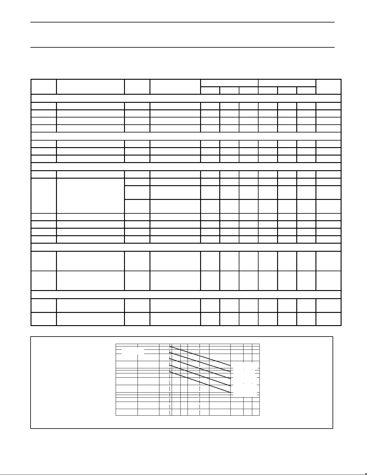
Figure 3. Frequency vs RT, CT NE/SE5562
V
OL
Low output voltage
Page 7
Philips Semiconductors Product specification
NE/SE5562Switched-mode power supply control circuit
1994 Aug 31
7
40
30
20
10
0
100
1k 10k 100k 1M
10M
GAIN (dB)
0
–30
–60
–90
–120
–150
–180
PHASE (DEG)
FREQUENCY
TA = 25°C
CLOSED-LOOP GAIN
PHASE
SL00391
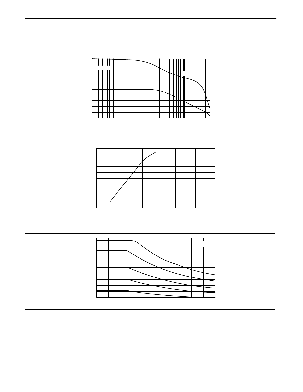
Figure 4. Error Amplifier Closed-Loop Response
PWM INPUT VOLTAGE (V)
100
90
80
70
60
50
40
30
20
10
0
1 2 3 4 5 6 7 8 9 10
DUTY CYCLE (%)
VCC = 12V
TA = 25°C
SL00392
Figure 5. Duty Cycle vs PWM Input Voltage
FEED-FORWARD VOLTAGE (V)
TA = 25°C
DUTY CYCLE (%)
100
90
80
70
60
50
40
30
20
10
0
5 6 7 8 9 10 11 12 13 14 15
SL00393
Figure 6. Duty Cycle vs Feed-forward Voltage
Page 8
Philips Semiconductors Product specification
NE/SE5562Switched-mode power supply control circuit
1994 Aug 31
8
SUPPLY VOLTAGE (PIN 17)(V)
SUPPLY CURRENT (PIN 17) (mA)
22
20
18
16
14
12
10
8
6
4
2
0
0 2 4 6 8 10 12 14 16 18 20 22 24
TA = 25°C
SL00394
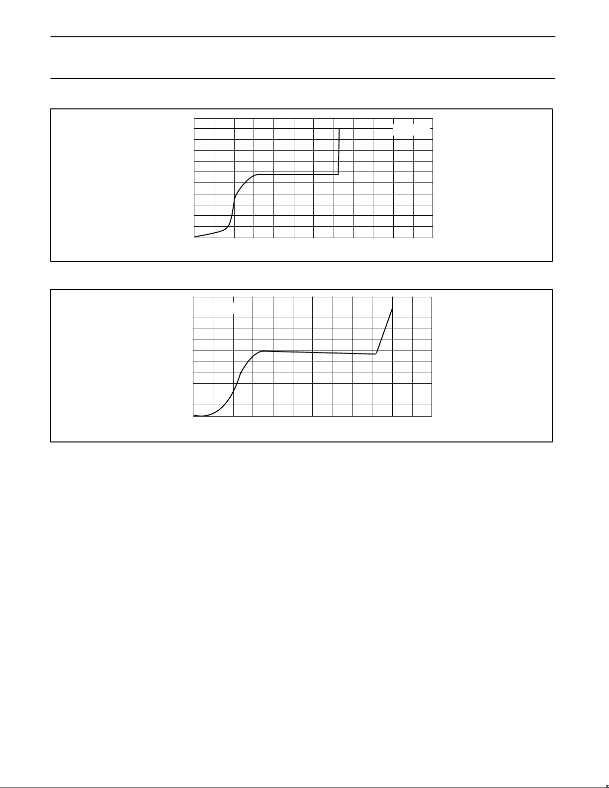
Figure 7. Current-Feed Characteristics
SUPPLY VOLTAGE (PIN 17)(V)
SUPPLY CURRENT (PIN 17) (mA)
22
20
18
16
14
12
10
8
6
4
2
0
0 2 4 6 8 10 12 14 16 18 20 22 24
TA = 25°C
SL00395
Figure 8. Voltage-Feed Characteristics
Page 9
Philips Semiconductors Product specification
NE/SE5562Switched-mode power supply control circuit
1994 Aug 31
9
THE NE/SE5562 THEORY OF OPERATION
INTRODUCTION
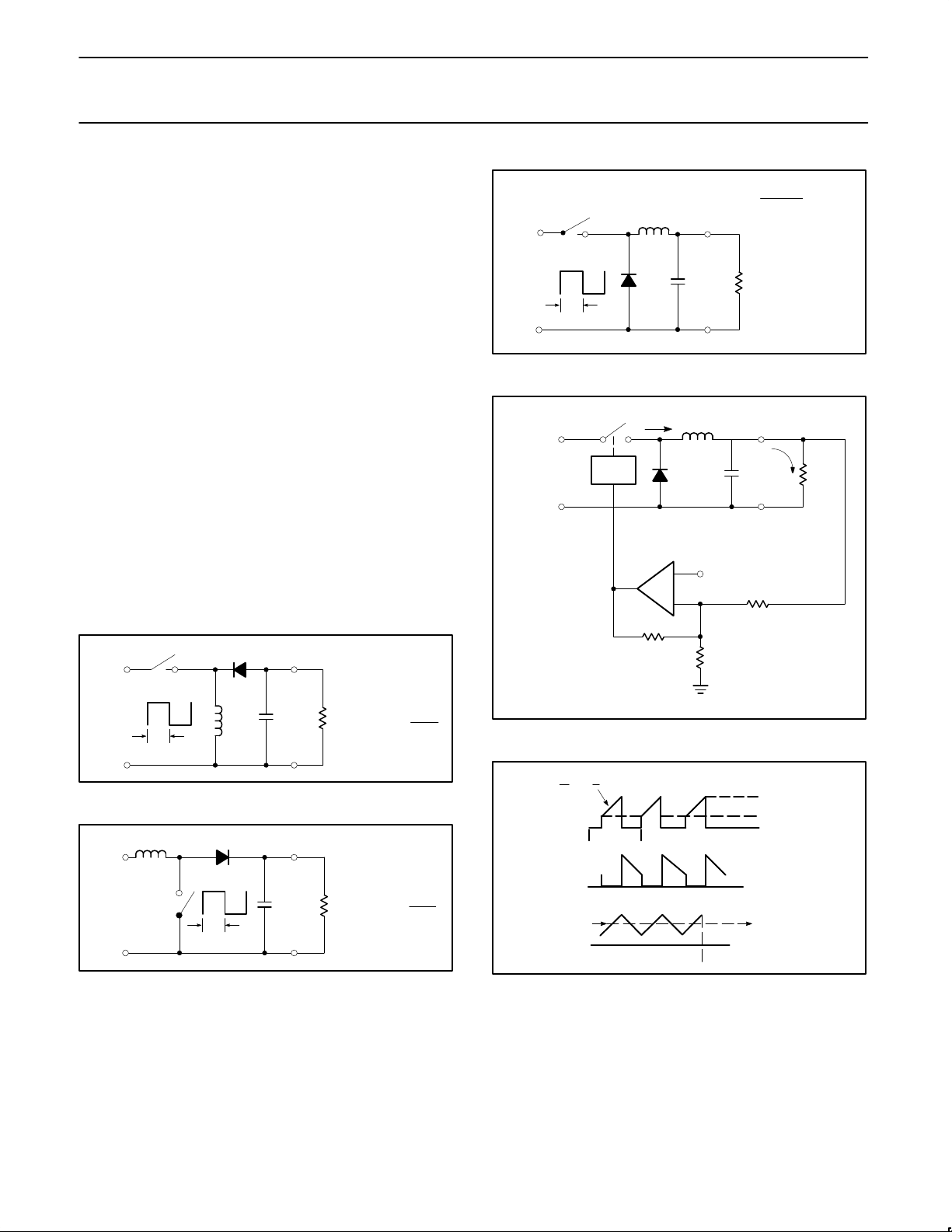
Switched-mode power conversion relies on the principle of pulsed
energy storage in an inductive or capacitive element. Capacitive
switched converters are typically used with low power systems for
which only tens of milliamperes are required. Medium and high
power converters tend to use inductive storage elements as shown
in Figures 9-11 with which a single switch may be moved around to
create step-up (flyback) positive or negative polarity and step-down
(forward or buck) conversion from a fixed-voltage source. The
relationship between input and output voltage in each case is
controlled by the switching on-to-off ratios, which is termed duty
cycle. Duty cycle modulation is the common factor in this basic type
of power control mechanism. By adding a high-gain operational
amplifier, having one input tied to a stable DC reference voltage,
configured in a negative feedback loop to maintain a constant output
voltage as shown in Figure 12, the switched-mode controller
becomes a dynamic voltage regulator. It is this single-switch
topology that is most readily adapted to the NE/SE5562 SMPS
Control IC.
The ability to switch inductor currents at rates up to 600kHz with
state-of-the-art power FETs makes the design of small, efficient
switching power converters an attainable reality. Protective features
such as programmable slow-start and cycle-by-cycle current limiting
allow safe, maintenance-free power supplies to be mass-produced
at reduced cost to the manufacturer. Integrated technology makes
long-term reliability a predictably achievable goal.
V
OUT
V
IN
1
R
L
D
O
SW
V
IN
L
C
O
δ
–
+
COM
SL00396
Figure 9. Negative Output Flyback Converter
V
OUT
V
IN
1
R
L
D
O
SW
V
IN
L
C
O
δ
–
+
COM
+
SL00397
Figure 10. Positive Output Flyback Converter
WHERE
tSWON
T
PERIOD
V
OUT
V
IN
R
L
D
B
SW
V
IN
L
C
O
δ
–
+
COM
+
SL00398
Figure 11. Forward Converter (Single Inductor) Step Down
PWM
L
C
REGULATED
OUTPUT
A
+
–
V
IN
UNREGULATED
DC
V
REF
I
SW
I
L
R
L
R
F
R
2
R
1
+
–
+
–
SL00399
Figure 12. The Forward (Buck) Converter (V
OUT
= VIN(δ))
i
t
E
L
SWITCH
CURRENT
DIODE
CURRENT
TOTAL
INDUCTOR
CURRENT
MAGNETIZATION
CURRENT
LOAD CURRENT
AVERAGE
INDUCTOR
CURRENT
SL00400
Figure 13. PWM Switching Waveforms
Page 10
Philips Semiconductors Product specification
NE/SE5562Switched-mode power supply control circuit
1994 Aug 31
10
1
3
2 1
+7.50V
CURRENT
STEERING
VOLTAGE
FEEDBACK
8
ERROR
AMP
+3.80V
10
PWM
COMPARATOR
+
–
–
–
–
OUTPUT TO
LATCH RESET
SAWTOOTH
GENERATOR
TO DELAY
CIRCUIT
TIME BASE
SIGNAL
ACTIVE LOW
0.8V
EXT.
SYNC
11
(5.25V)
28k
(1.70V)
3k
DISCH.
FF
S
R
–
+
–
+
FEED-
FORWARD
+
+
V
Z
C
T
R
2
R
3
I
O
V
H
SL00401
Figure 14.
THE NE/SE5562 THEORY OPERATION
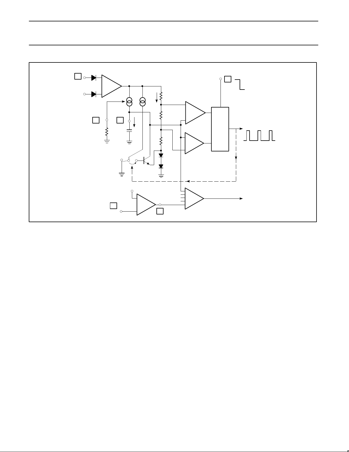
The Sawtooth Oscillator
The sawtooth oscillator consists of a gated charge-discharge
capacitor circuit with threshold comparators setting the peak and
valley voltages of the ramp. The resistor divider R1-3 is supplied
with a source voltage derived from either V
Z
(7.50V) minus two
diode drops, or, when feed-forward is in control, a voltage greater
than V
Z
and proportional to the main supply voltage. The nominal
upper threshold voltage is 5.25V and the lower threshold 1.70V .
These then determine the sawtooth peak and valley voltages,
respectively.
Operation
Beginning with the charge cycle, ramp voltage builds up on the
timing capacitor due to a constant current supplied to the node at
Pin 2. When capacitor voltage reaches the upper threshold,
comparator A switches, setting the latching flip-flop. The output of
the latch goes high, generating a clock pulse. The discharge
transistor is simultaneously turned on, reducing charge on the timing
capacitor to the point at which the lower threshold voltage, 1.70V , is
reached. The lower comparator is then activated, resetting the latch
and terminating the clock pulse. Note that the discharge transistor is
referenced to the same return diodes as the threshold resistor
divider and the discharge current is made to track with the charge
current. This charge and discharge tracking results in a true
sawtooth waveform even at extended frequencies. Figure 17 shows
a family of curves which explains the relationship between R
T
, CT,
and the frequency of the sawtooth generator. The data sheet shows
the initial accuracy of the oscillator at 60Hz and 600kHz.
THE PULSE WIDTH MODULATOR AND ERROR AMPLIFIER
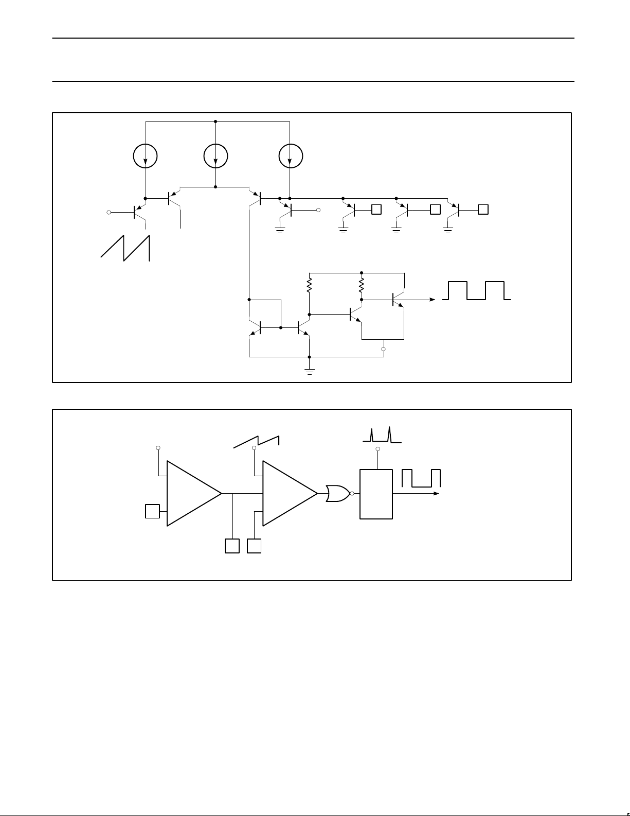
The PWM consists of a multi-input voltage comparator (Figure 15)
having its positive input tied to the sawtooth ramp voltage and the
various negative inputs referenced to ORed control signal nodes.
The primary control signal is the error amplifier output voltage node
which sets the active duty cycle termination point of the PWM output
waveform. As the error amplifier input signal derived from the power
supply load voltage varies, for instance in a negative direction, the
amplifier output moves upward, raising the PWM comparator toward
longer duty cycles at the output on Pin 19. The start-up sequence
begins with zero voltage at the input to the error amplifier. Since this
could signal an open feedback loop, the loop fault comparator on
Pin 8 clamps the PWM duty cycle until the feedback voltage
exceeds 0.955V. A second comparator monitors the duty cycle
control, Pin 5, with the same threshold level, inhibiting the output via
the start-stop latch (Figure 16).
The charging of the slow-start capacitor provides a controlled
ramp-up of the output duty cycle and a resultant gradual increase in
energy fed to the output magnetics.
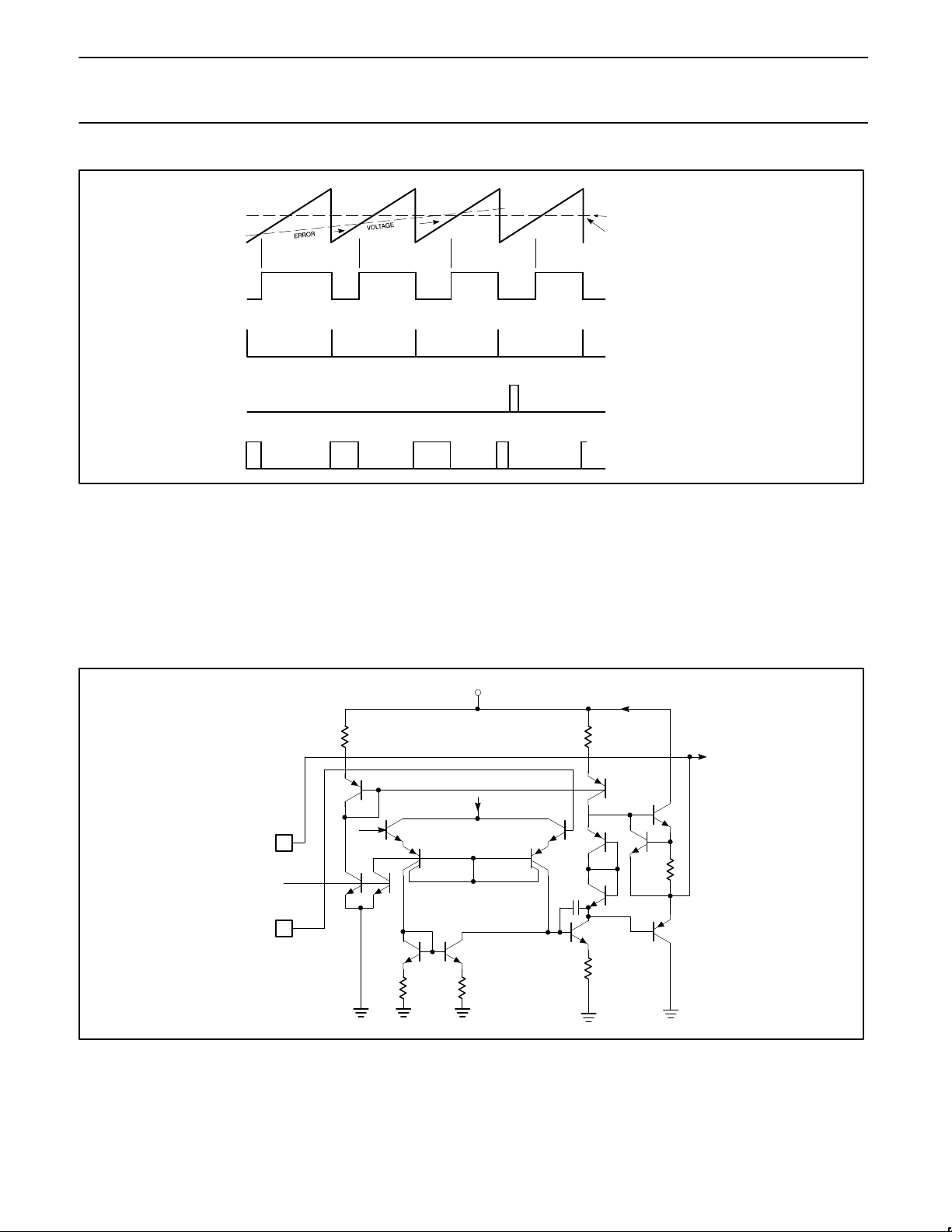
The dynamic response of the PWM comparator is shown in the
simulated waveform drawing of Figure 17. The error amplifier output
voltage is depicted as sloping positive (increasing) with time as
referenced to the sawtooth waveform. This causes the duty cycle to
increase with time. This is an indication of an increasing load on the
power supply as output voltage is decreasing. The Pin 5 (δ
MAX
)
control voltage is also superimposed midway on the sawtooth,
indicating the limits of duty cycle increase as the output waveform
no longer increases in duty cycle after the δ
MAX
threshold is
crossed. A hypothetical overcurrent pulse (Pin 14) is shown to
illustrate cycle termination immediately at the output (Pin 19).
Page 11
Philips Semiconductors Product specification
NE/SE5562Switched-mode power supply control circuit
1994 Aug 31
11
SAWTOOTH
+
DELTA
MAX
CONTROL
PWM SIGNAL
TO OUTPUT
NOR GATE
SAWTOOTH
UPPER
THRESHOLD
ERROR
AMP
OUT
MODULATOR
IN
9k
2.5k
10
4 5
(–) (–) (–) (–)
100µA
35µA 35µA 35µA
+V
Z
V
H
SL00402
Figure 15. PWM Comparator
DELAYED CLOCK
TO OUTPUT
STAGE
NOR
OUTPUT
LATCH
R
S
PWM
+
–
–
8
10 5
+
–
DUTY
CYCLE
CONTROL
+3.80V
V
REF
δ
SL00403
Figure 16. The Duty Cycle Control Circuit, Pulse Width Modulator, and Error Amplifier, Reference, and Output Latch
Page 12
Philips Semiconductors Product specification
NE/SE5562Switched-mode power supply control circuit
1994 Aug 31
12
(OUTPUT)
PIN 14
+0.528V
SAWTOOTH
WAVEFORM
PIN 5
PWM COMPARATOR
(INTERNAL)
FLYBACK PULSE
(INTERNAL)
CURRENT
SENSE INPUT
PIN 19
δ MAX LEVEL
SL00404
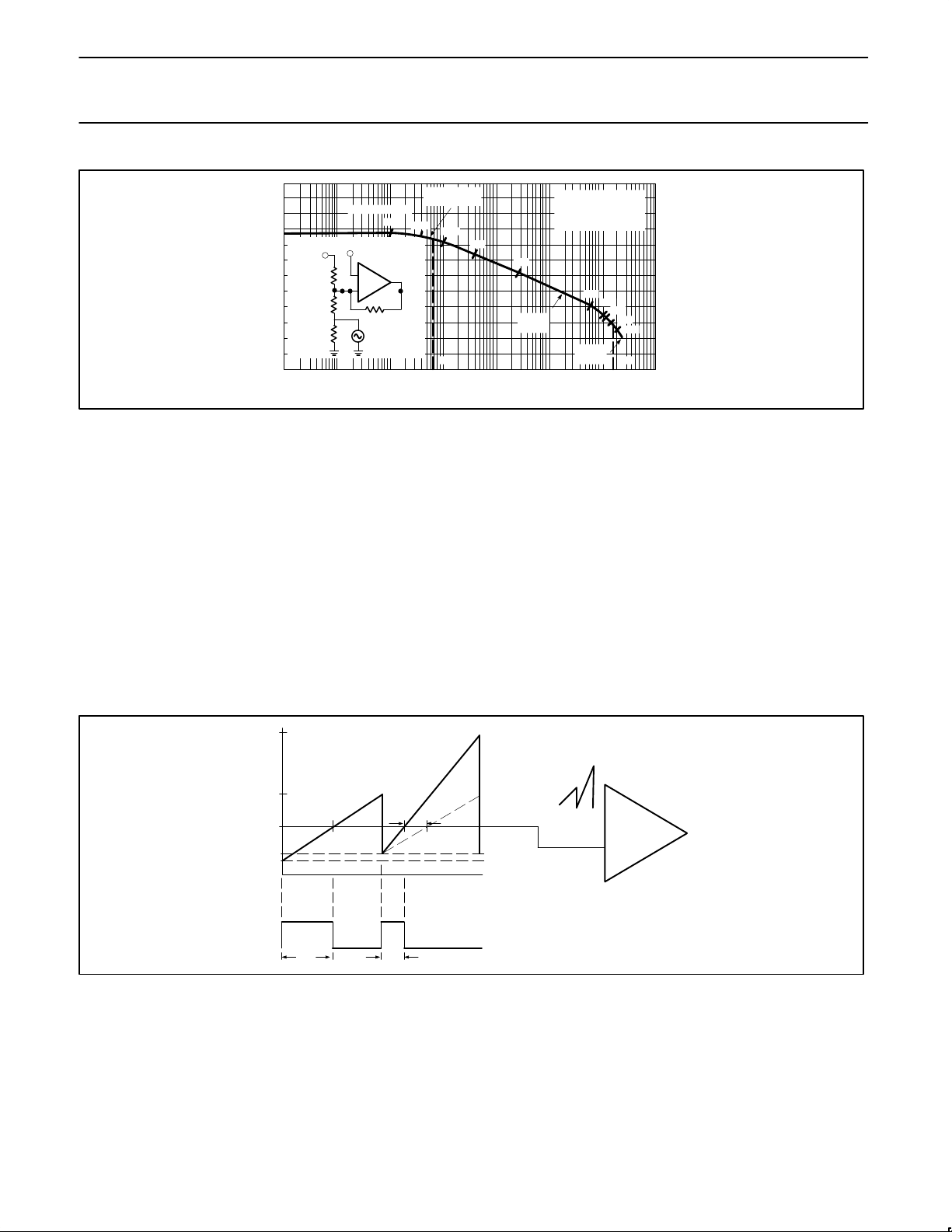
Figure 17. Duty Cycle vs Feedback Error and Overcurrent Sense
The error amplifier’s non-inverting input is tied to a bandgap
reference of 3.80V, accurate to ±2% at 25°C. The temperature
stability of the voltage reference is 30ppm/°C.
The error amplifier is designed for an open-loop gain of 86dB having
a small-signal unity gain bandwidth of 3MHz. Closed-loop gain is
stable to 10dB, as shown in Figure 19. The DC output excursion of
the amplifier is capable of controlling the full PWM range of 0 to
95%. The amplifier can sink 10mA and source 5mA. The nominal
DC output for 50% duty cycle is 3.55V. Feedback control resistor
value may range from 1kΩ to 240kΩ without overload or instability.
However, low closed-loop gains must be compensated by lag lead
network techniques for optimum stability. Loop compensation
networks may intersect the open-loop gain curve with a slope 2
closure and must then be compensated to maintain overall phase
and gain margin (Figure 18).
+VZ (7.50V)
ERROR AMP
OUT
N BIAS
FEEDBACK
SENSE
10
8
3.80
6k 2.5k
7pF
30
6k
6k
V
Z
V
Z
V
REF
SL00405
Figure 18. Error Amplifier
Page 13
Philips Semiconductors Product specification
NE/SE5562Switched-mode power supply control circuit
1994 Aug 31
13
80
70
60
50
40
30
20
10
0
1 10 100 1000 10000 100000 1000000
FREQUENCY (Hz)
(8)
(10)
10M
50
360
5k
OFFSET
ADJUST
+
–
+V
REF
3.75V
PHASE DELAY
EST. –3dB
FREQUENCY
160°
143°
130°
98°
95°
92°
NE5562
ERROR AMPLIFIER
PHASE/AMPLITUDE
RESPONSE
SLOPE
= (–)1
SLOPE
= (–)2
80°
83°
70°
32°
f
P2
A A (dB)
CL OL
≈
f
P1
SL00406
Figure 19. Error Amp Response
FEED-FORWARD COMPENSATION (PIN 1)
To provide a means of automatically improving line-to-load voltage
regulation, a technique called feed-forward regulation is made a part
of the NE/SE5562 active mechanism. Referring back to the diagram
for the sawtooth oscillator, note that Pin 1 is capable of changing the
internal supply voltage to the charging circuit for the timing capacitor,
C
t
.
With a nominal duty cycle of 30%, for instance, increasing Pin 1
voltage by 1V from 10.3 to 11.3 will reduce the output duty cycle by
approximately 5%. Thus, a primary voltage change has caused a
decrease in volt-seconds (duty cycle X primary volts) of 5/30 or 16%
(Figure 6). The result is a small over-compensation in the output
energy, but an overall safe margin in transformer flux.
The mechanism which produces inverse duty cycle modulation is
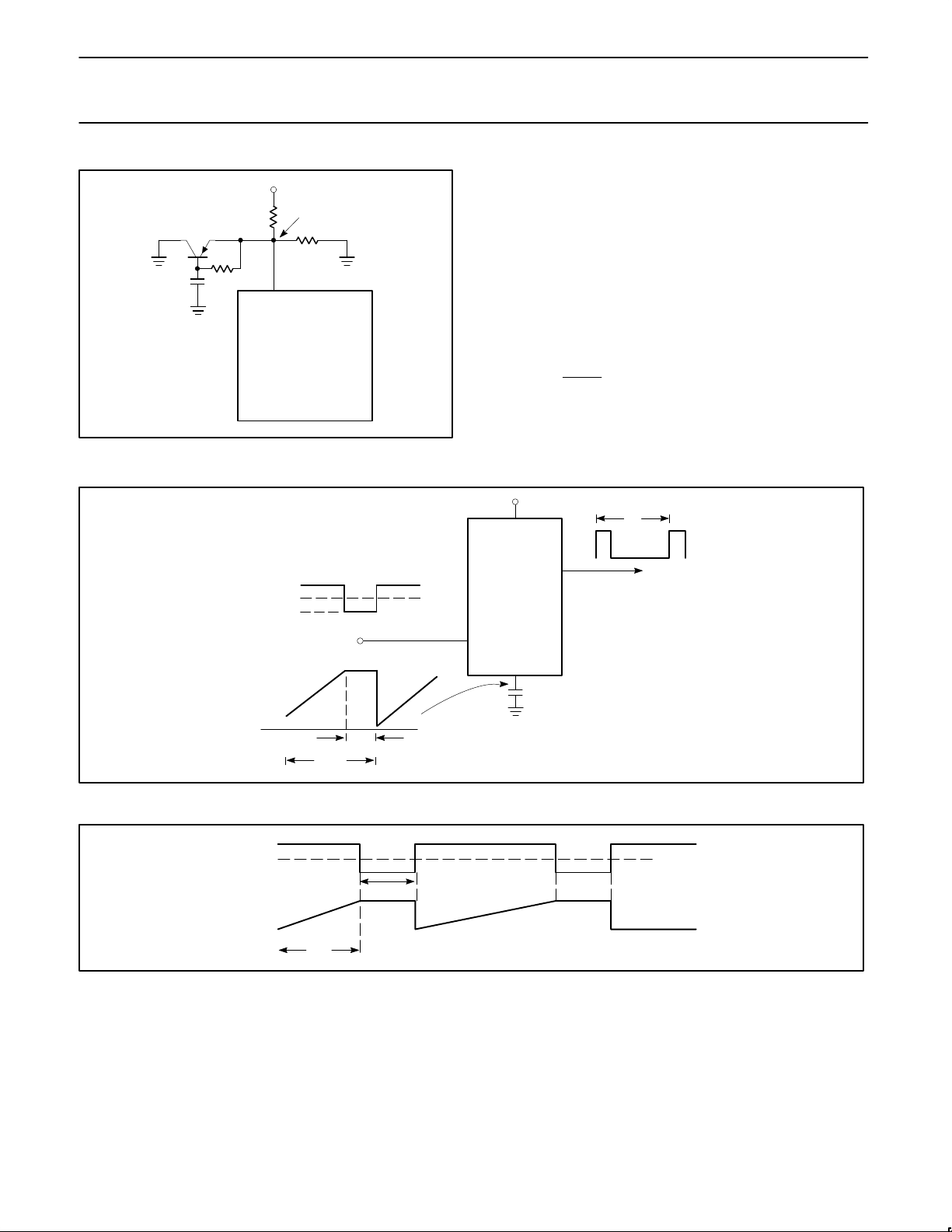
shown in Figure 20. Increasing Pin 1 voltage beyond the value of V
z
(7.50V) increases the charge rate on CT, causing the duty cycle to
be terminated earlier for each cycle that input voltage is increased.
The threshold voltages at the sawtooth limit comparator reference
inputs are changed with Pin 1 also in order to offset any change in
oscillator frequency.
The secondary benefit of using feed-forward is the attenuation of
any low-frequency AC riding on the DC supply before it reaches the
regulated output.
Note that a start delay circuit is added to the Pin 1 divider in order to
prevent internal race conditions during initial power-up. Once the
turn-on transient has decayed, normal operation of the feed-forward
circuit is assured. Figure 21 shows an RC delay placed in a base
clamping circuit to provide reliable starting.
LINE VOLTAGE SENSE
2V
Z
V
Z
V
TH
V
TH
PWM
COMPARATOR
+
–
TT
δ δ
SL00407
Figure 20. Feed-Forward
Page 14
Philips Semiconductors Product specification
NE/SE5562Switched-mode power supply control circuit
1994 Aug 31
14
2N3906
220k
NE/SE5562
1
V
FFWD
0.2µF
SL00408
Figure 21. Feed-forward Turn-On Delay Circuit
SYNCHRONIZATION
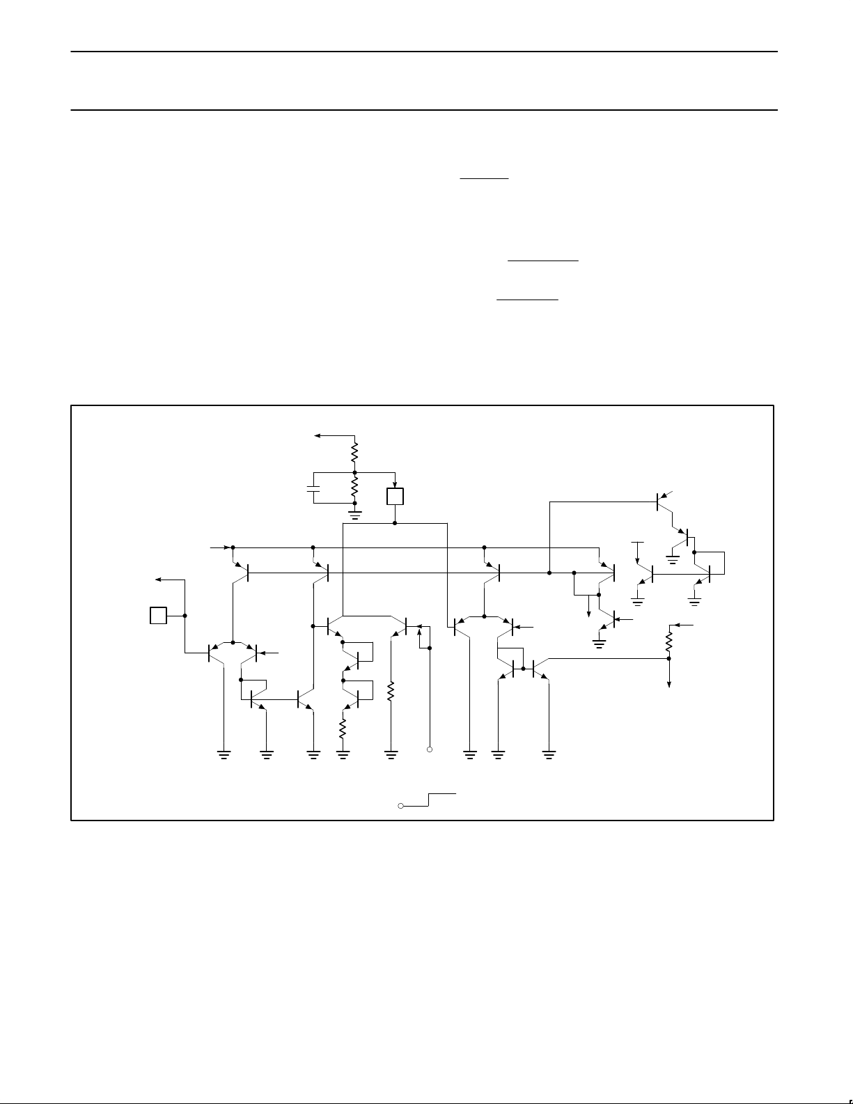
The synchronization of the sawtooth oscillator to an external pulse
of negative-going polarity is shown in Figure 22. When the sync
input pulse crosses the 1.5V threshold, negative, the sawtooth
oscillator is prevented from discharging the timing capacitor, causing
the charge voltage on the capacitor to remain high (5.25V) until the
sync pulse again goes above 1.5V, allowing reset. This action
stretches the period of the oscillator and results in a lower frequency
under-synchronization control than the free-running frequency.
The following relationship holds—
f
free*run
u f
sync
f
sync
+
1
t
0
)
A typical recommended starting point in calculating frequency for
synchronous operation is to set the free-run frequency
approximately 10% higher than the sync frequency. Then set the
pulse width, τ, to 10% of t
0
, the free-run period, with the desired new
frequency determined by the sum as above.
11
1.5V
SYNC
+
2
19
T
T
d
NE/SE5562
+V
CC
SL00409
Figure 22. Synchronization Signals
SIGNAL
PIN 11
SYNC
SAWTOOTH
WAVEFORM
+1.5V
T
O
τ
SL00410
Figure 23. Sync Signal Relationship to Controlled Sawtooth Waveform
DUTY CYCLE LIMIT (PIN 5)
The forward or buck converter, and even the flyback converters,
may require an automatic duty cycle limit to prevent transformer
saturation or unstable behavior. A special input provides access to
the PWM comparator for this purpose. As discussed previously in
regard to the error amplifier, increasing load demand may drive the
system current beyond safe limits. A simple solution is the
placement of a duty cycle limit within the system dynamic response
before this can occur. Figure 15 shows the PWM comparator with its
multiple input ports. All are inverting in polarity and provide a lowest
priority level sensing circuit. The lowest level on Pin 4, 5, or 10 gains
control of the duty cycle limit. During normal operation, the δ
MAX
circuit sends a continuous threshold signal to the PWM comparator,
setting a fixed limit on how much the error amplifier is allowed to
increase the duty cycle in response to load demand. Figure 24
shows the circuit within the NE/SE5562 which actually controls duty
cycle as listed below:
1. Duty cycle ramp-up (slow-start) during power-up. Time constant
controlled by external R, C ramp voltage at Pin 5.
Page 15
Philips Semiconductors Product specification
NE/SE5562Switched-mode power supply control circuit
1994 Aug 31
15
2. Slow-start if remote ON/OFF is actuated, if OC2 threshold trips,
demagnetization/overvoltage is sensed, or low supply voltage to
the internal regulator is sensed (VS≤8.45V).
3. Note that Pin 8 is monitored by the loop fault comparator. When
the regulated supply feedback drops below this threshold level
(0.955V), the duty cycle is clamped by two diodes in series with
a 2kΩ load across Pin 5 to ground. This implies a minimum duty
cycle condition as long as the low output level remains.
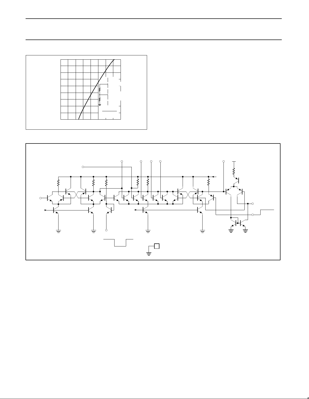
Referring to the graph in Figure 25, the designer may choose a
divider ratio which, when referenced to V
Z
, 7.5V, provides an easy
duty cycle limit control. For example, a 50% limit results in a ratio of
0.48. Setting R
2
at a nominal value between 10 and 20kΩ and
solving for R
1
, the proper limit is obtained.
Example:
A duty cycle limit of 50% is required for a forward converter.
R
2
= 10kΩ, find R
1
R
2
R1) R
2
+ 0.48
∴ R2 = 0.48 (R1 + R2)
0.48R
1
= R2 – 0.48R
2
N R
1
+
R
2
(1 * 0.48)
0.48
+
10k (0.52)
0.48
= 10.8kΩ
DELTA
MAX TO
PWM COMP
SLOW
START
CAP
5
ERROR
AMP IN
8
0.955V
LOOP
FAULT
COMP
2k
50
‘A’
FROM
START/STOP
LATCH
STOP
+
SLOW
START
COMP
SLOW
START
COMP
OUT
9k
1.5V
0.9V
N BIAS
0.9V
R
1
R
2
C
SS
V
Z
V
Z
36µA
SL00411
Figure 24. Duty Cycle Limit Control
Page 16
Philips Semiconductors Product specification
NE/SE5562Switched-mode power supply control circuit
1994 Aug 31
16
MAXIMUM DUTY CYCLE %
R
2
R
1
)
R
2
V
Z
+ 7.50
V
90
80
70
60
50
40
30
20
10
0
0.2
0.3 0.4 0.5
0.6 0.7
0.8
0.1
DUTY
CYCLE
CONTROL
SL00412
Figure 25. Maximum Duty Cycle
LOW SUPPLY
SENSE
TO
OUTPUT
NOR
OC2
SENSE
DEMAG/OV
SENSE
REMOTE
ON/OFF
TO
OUTPUT
NOR
R79
10k
Q282
Q284
Q283
1.5V
R78
10k
Q277
Q279
Q278
Q276
Q260
Q275Q274Q273Q272Q271Q270
Q269
Q266
Q265
Q264Q262
Q261
Q263
R73
10k
R74
10k
R75
18k
R76
15k
R77
10k
Q267
Q268
Q280
Q281
Q283B Q283A
DISCHARGE
SLOW-START
COMPARATOR
RESET
+
BULK
SENSE
RESET
0V
SIGNAL
GND
20
START STOP LATCH
C
SS
SHUTDOWN LATCH
+
V
Z
OC ACCUM
SL00413
Figure 26. Start-Stop/Shutdown Latches
Page 17
Philips Semiconductors Product specification
NE/SE5562Switched-mode power supply control circuit
1994 Aug 31
17
THE START-STOP CONTROL SEQUENCE
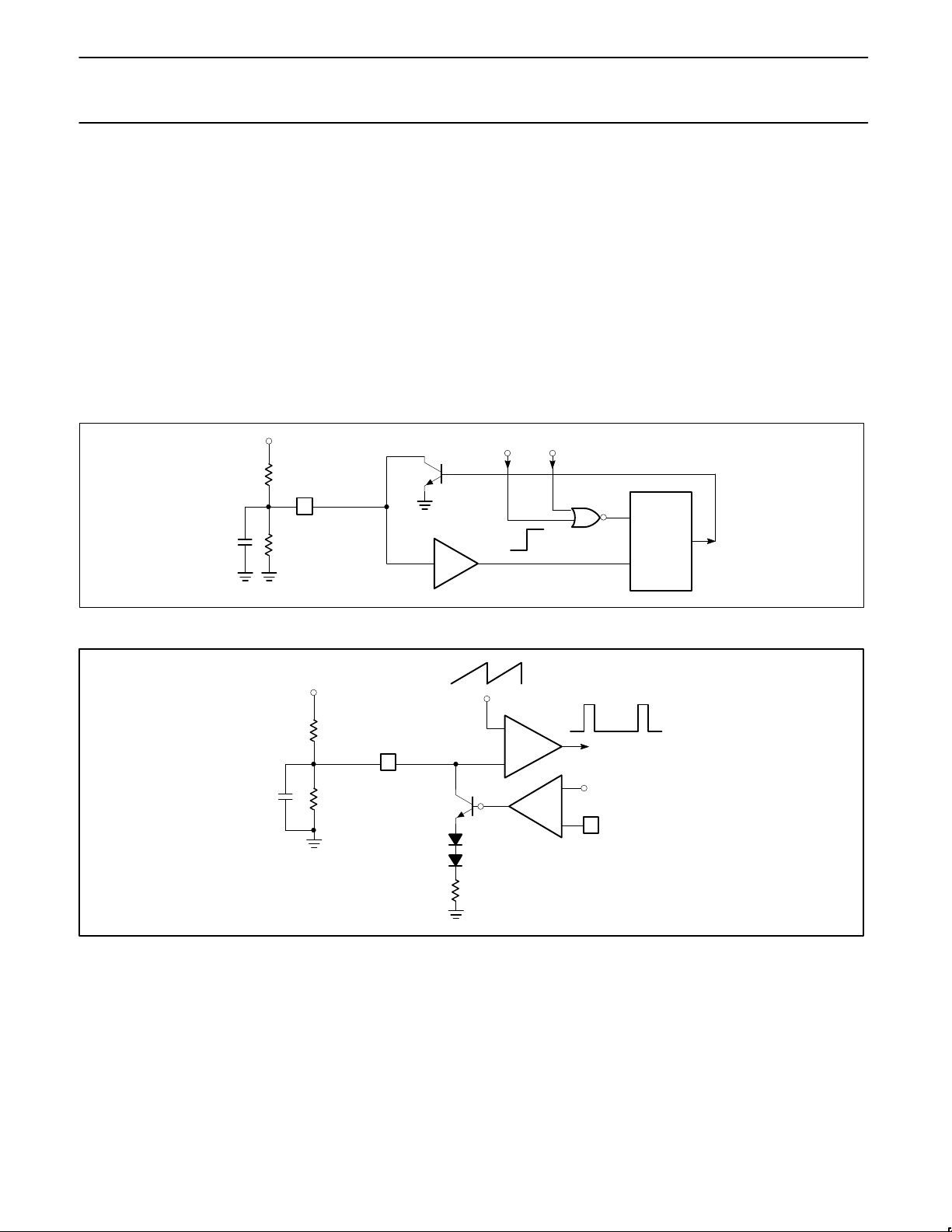
The start-up circuit involves a sequential set of conditions which
progresses as follows: power-up after OFF condition or remote ON
after OFF. Initially, 0V exist on the supply output, causing zero
feedback volts on Pin 8. The slow-start capacitor is discharged,
forcing Pin 5 to 0V, having been clamped by the internal discharge
transistor. Internal supply regulator input exceeds 8.45V, releasing
low voltage shutdown condition with Pin 5 below 0.955V . The
slow-start comparator output goes high, resetting the start/stop
latch, sending a low output signal to the output stage power NOR
gate. The PWM signal is then enabled to feed the output drive
circuits, starting energy flow through the magnetics. However,
instantaneously the power supply output is still below 0.955V and
the loop fault comparator forces the PWM to remain at a minimum
duty cycle. The equivalent circuit at this instant in the start-up cycle
which exists at Pin 5 is shown in Figure 28.
The actual minimum duty cycle is determined by the parallel source
resistance of R
1
and R2 combined with the shunt loading internal to
Pin 5. High values of divider resistance, 20-30kΩ, will supply less
shunt current to Pin 5 and create a lower modulator duty cycle, while
lower values of R
1
and R2 (5-10kΩ) will generate a higher modulator
voltage and a greater resultant minimum duty cycle.
As the power conversion circuits become active and Pin 8 feedback
voltage increases above 0.955V, the duty cycle network is
unclamped; duty cycle increases, controlled by the RC time constant
R
1
||R2.CSS, and as output voltage brings the feedback voltage up to
equal the reference voltage, 3.80V , the error amplifier takes control
and the supply is in regulation.
+7.50V
DISCHARGE
DEMAG
0V
OC2
START/
STOP
LATCH
S
R
Q
–
+
SLOW-START
COMPARATOR
0.955V
R
1
5
R
2
C
SS
SL00414
Figure 27. Slow-Start Comparator
5
R
2
5
7.50V
0.2V
1.4V
2k
ON
LOOP FAULT
COMPARATOR
FEEDBACK
VOLTAGE
SENSE
MINIMUM
DUTY CYCLE
PWM
COMP
+
–
–
–
R
1
C
SS
V
MOD
SL00415
Figure 28. Loop Fault Comparator and Minimum Duty Cycle Clamp
The stop or shutdown sequence is initiated by any of the following
conditions:
a. Supply voltage (bulk) sense below 3.80V at Pin 12.
b. Pin 17 below 8.45V or Pin 7 current below level (less than
9mA).
c. Remote ON/OFF voltage at Pin 6 greater than 2V .
d. Sustained OC2 causing C
DLY
to charge above 3.80V (current
sense on Pin 14 continuously above 0.645V peak).
Page 18
Philips Semiconductors Product specification
NE/SE5562Switched-mode power supply control circuit
1994 Aug 31
18
DUAL-LEVEL OVERCURRENT COMPARATORS
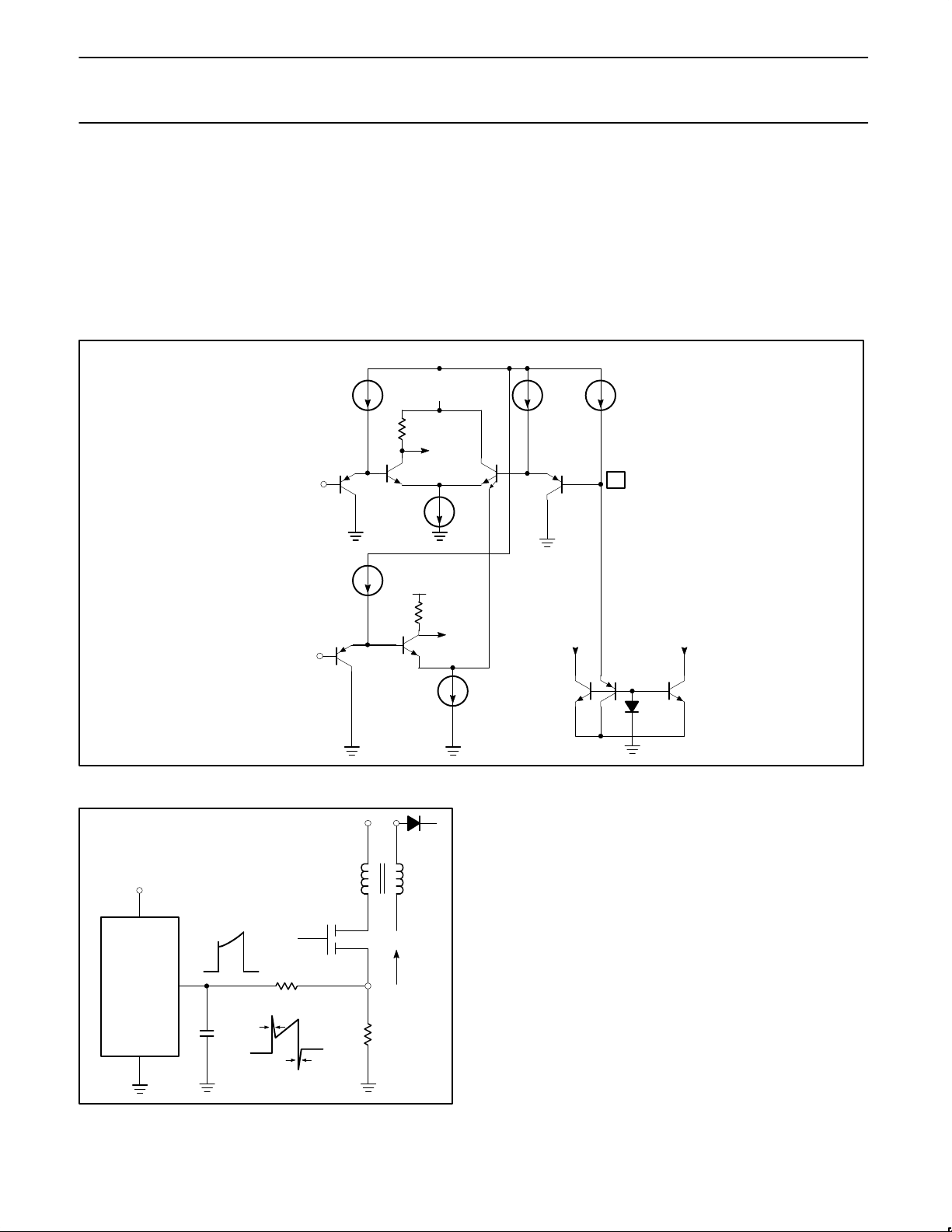
The overcurrent sensing circuit (Figure 29) consists of a single PNP
input buffer with emitter-follower tied to V
Z
, 7.50V, feeding into the
base of an NPN split-emitter transistor. This forms the input node to
a set of dual-level voltage comparators with references of 0.528 and
0.645V, respectively. Current sources for the comparator are fixed
biased NPNs.
The typical transition time delay for an overcurrent fault is 300ns.
Bias current at the input averages 500nA.
If the overcurrent sense feature is not used, it is recommended that
Pin 14 be tied to ground.
When used for sensing current-derived voltage impulses from the
primary driver, a high-speed, low-impedance transient filter network
is advised. An example is shown in Figure 30. Keep C
F
close to the
NE/SE5562.
REFERENCE
0.645V
REFERENCE
0.528V
1.5V
3k
OC1
0.528V 0.645V
CURRENT
SENSE
INPUT
OC2
1.5V
14
3k
135µA 135µA 135µA
135µA
100µA
V
Z
= 7.50V
100µA
SL00416
Figure 29. NE/SE5562 Overcurrent Comparator
NE/SE5562
10% CARBON
+V
CC
500-1000Ω
C
F
R
SH
I
MAG
SL00417
Figure 30. Transient Suppression
THEORY—OC1 AND OC2
Overcurrent Logic and Delay Capacitor Operations
The circuit takes a voltage input from Pin 14 and compares the level
to a dual reference comparator with trips at 0.53 and 0.65V . The
lower trip point actuates cycle-by-cycle shutdown of the output stage
with an intrinsic delay of 400ns. The second level actuates the
slow-start function. In addition, there exists a separate
housekeeping circuit whose function is to terminate operation of the
output stage if its threshold is exceeded. This involves a time delay
circuit based on two separate switchable current sources, OC1 and
OC2. The time delay capacitor allows the user to program shutdown
of the system after a predetermined number of overcurrent cycles
have occurred within the period set by the ramp-up of the delay
capacitor. Once shutdown has occurred in this manner, external
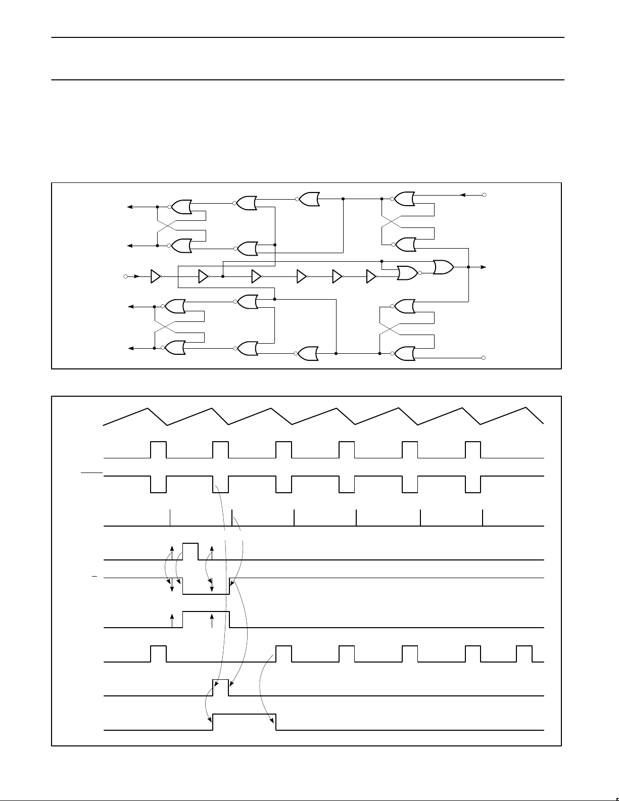
reset is required to restart the system. Referring to the logic block
Figure 31, which controls the gating of the two charge pumps into
the delay capacitor at Pin 16, the complete signal flow may be
traced. Logic signals from the overcurrent 1 and 2 comparators are
gated by the clock and delayed clock signals generated by the
Page 19
Philips Semiconductors Product specification
NE/SE5562Switched-mode power supply control circuit
1994 Aug 31
19
sawtooth oscillator. The complete sequence for an overcurrent fault
may be understood by referring to Figure 32 for OC2. Here it is
shown that an OC2 signal exists indicating that the 0.65V threshold
has been exceeded by a signal at Pin 14.
Note that an overcurrent pulse within a particular clock frame turns
on the respective OC2 charge ramp during the entire next clock
frame. Consecutive overcurrent pulses of either OC1 or OC2
magnitude will activate the selected charge pump for the total
duration that such overcurrent occurs. The charging cycle will
continue until the delay capacitor reaches the 3.86V trip level.
A
B
C
Q
OC2
CLOCK
OC1
OC1 DLEAYED
OC2 DELAYED
OC2
LATCH
OC2 IN
OC1 IN
OC1
LATCH
DELAYED
CLOCK
OUT
A
A
A A
A
A
A A
A
A
A
A
A
A
AAAA
A
A
A
B
B
B
B
B
B
B
B
B
B
B
B
B
C
C
C
C
C
C
C
C
C
C
C
C C
C
C
C
C
C
C
Q
Q
Q
SL00418
Figure 31. Overcurrent Logic
CLOCK
SAWTOOTH
DELAY
CLOCK
OC2
R
S
Q
PUMP
Q
B
Q
A
CLOCK
LET OC2 GO UP AT ANY TIME BETWEEN DELAY CLOCK RISES AND CLOCK RISES
SL00419
Figure 32. Fault Cycle
Page 20
Philips Semiconductors Product specification
NE/SE5562Switched-mode power supply control circuit
1994 Aug 31
20
OC2 DELAY TIME (MILLISECONDS)
3.86V
0.00V
100 200 300
3.66V
0.00V
10 20 30 40 50 60 70 80
OC1 DELAY TIME (MILLISECONDS)
(neglecting recycle dfelay)
0.1µF
0.5µF
1µF
C
DELAY
1µF
5µF
10µF
C
DELAY
SL00420
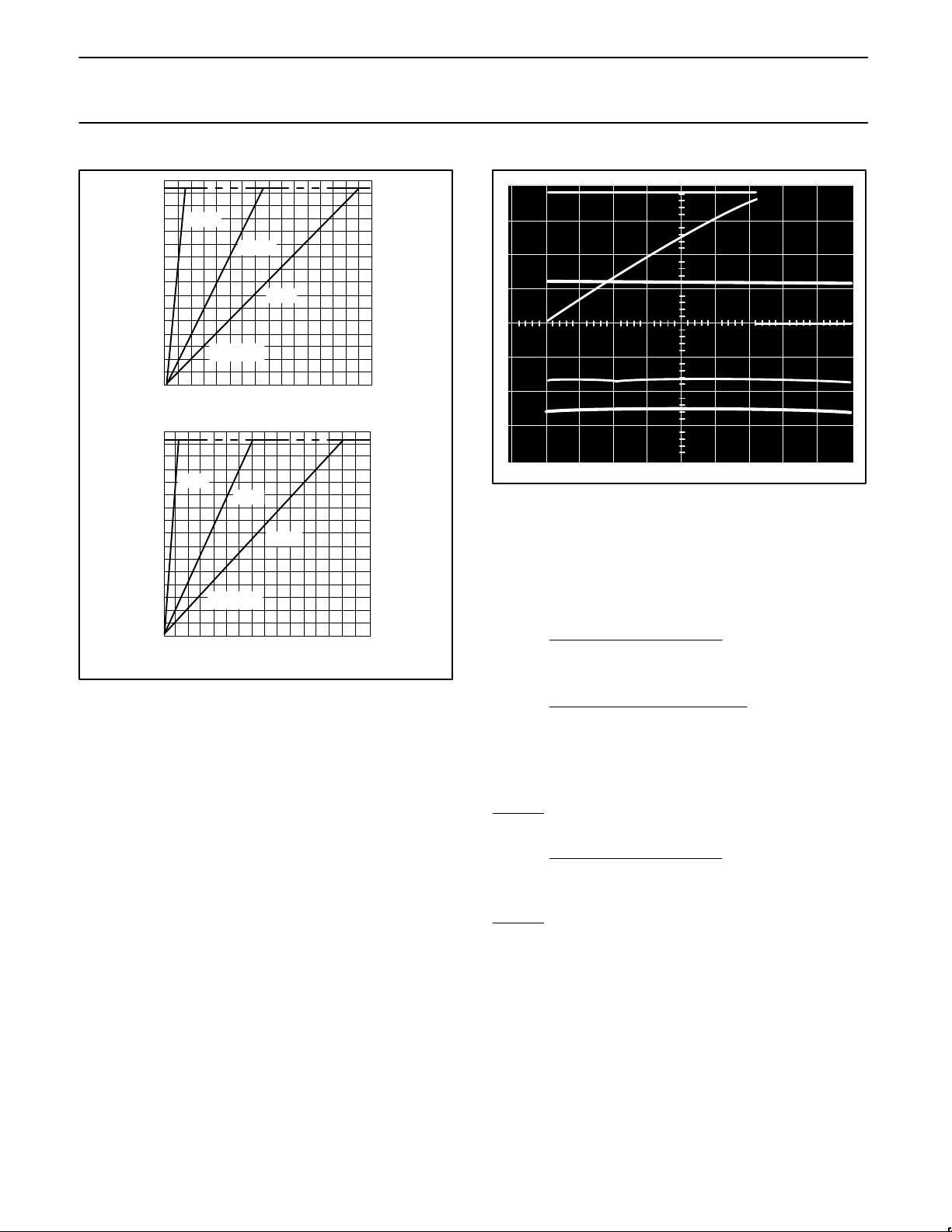
Figure 33. Overcurrent Shutdown Function
CALCULATING THE DELAY CAPACITOR
Actual delay time for a given capacitor value at Pin 16 may be
estimated using the graphs in Figure 33 for OC1 and OC2. By first
determining the allowable overcurrent time product for a particular
power converter, a capacitor delay value may be calculated.
Note that the OC1 charge pump is typically 13µA while OC2 pumps
550µA into the capacitor. If the exact value is to be calculated for a
particular delay requirement, use the following procedure:
1. Determine the level of overcurrent—OC1 or OC2.
2. Find the maximum delay time which the supply may safely sustain for this continuous overcurrent condition. Note that OC1 may
be activated on every cycle if OC2 is not reached, causing continuous charging of C-Delay. However, OC2 overcurrent detection causes the supply to go into slow-start shutdown (hiccup
SL00421
Figure 34. OC1 Ramp and Shutdown Delay
mode), on the first such pulse. OC2 delays are based on an
interrupted charging cycle with total cycle time determined by the
external slow-start delay capacitor duty cycle maximum
divider—time constant.
For a continuous OC1 overcurrent:
C
DLY
+
(13X10
*6
)(Delay time * sec)
3.86V
(1)
For a continuous OC2 overcurrent:
C
DLY
+
(550X10
*6
)(Delay cycles x 1ń fSW)
3.86V
(2)
Some downward adjustment of the OC2 capacitor value may be
necessary to compensate for the 1-2µA of discharge current at Pin
16 during the delay cycles.
Example:
A maximum of 100 OC2 current fault cycles is allowed.
f
SW
=400kHz, find C
DLY
C
DLY
+
(550X10*6)(100 x 1ń 4 x 10⁵)
3.86V
=0.036µF
Example:
OC2/C
DLY
Find number of OC1 cycles before shutdown with 0.036µF C
DLY
.
Page 21
Philips Semiconductors Product specification
NE/SE5562Switched-mode power supply control circuit
1994 Aug 31
21
Delay Time
(3.6 X 10
8
)(3.86V)
13 x 106A
=10.7ms
Total cycles shutdown
10.7 X 10
3
2.5 x 10
6
=4280
Figure 35 shows an actual OC1 charging cycle for continuous fault
current sensed at Pin 14 and a DLY = 1µF.
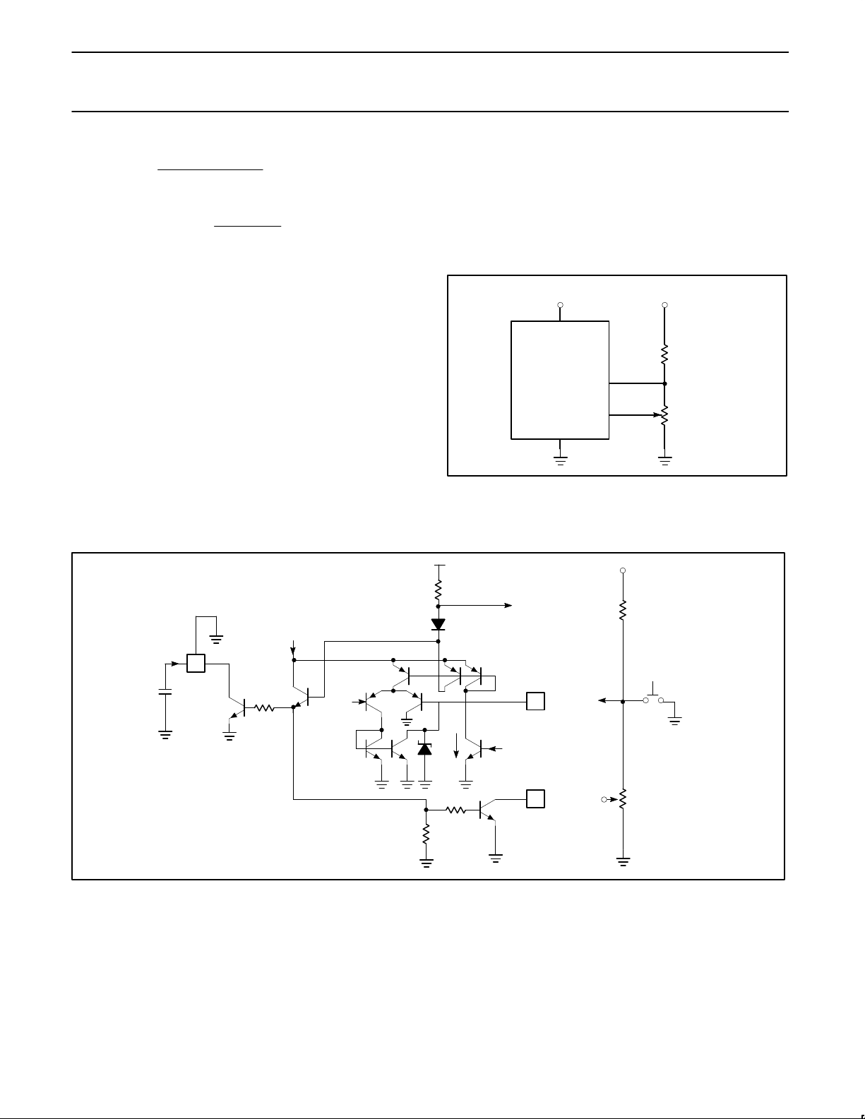
BULK-SENSE AUXILIARY COMPARATOR WITH SHUTDOWN
This circuit is intended to act as an automatic low-line detection
mechanism. As shown in Figure 35, a voltage divider is connected
from the main unregulated DC supply to Pin 12. The lower divider
resistor may be a potentiometer of 5-10kΩ resistance with
center-tap connected to Pin 13. The comparator which senses Pin
12 voltage is referenced to 3.80V and Pin 12 divider voltage must be
greater than this voltage by a sufficient margin to operate within the
prescribed low-line limits. For instance, if a line voltage drop of 25%
is considered the shutdown threshold, then V
12
should be calculated
for a nominal operating voltage as shown in Figure 35.
When the line voltage drops more than 25%, the output stage is
disabled. With the hysteresis connected as shown and the pot
adjusted near midway, the line voltage will have to exceed V
NOMINAL
before the supply will restart. The hysteresis control may then be
calibrated for the desired over-excursion before restart. This
prevents unstable circuit chatter.
The reset switch provides a means for resetting the shutdown latch
after overcurrent faults have charged C
DLY
to its trip threshold. This
also provides a discharge path for the delay capacitor. Figure 36
shows internal circuit.
V
BULK
HYSTERESIS
ADJUST
12
13
NE/SE5562
R
1
R
2
+V
S
SL00422
Figure 35. Bulk-Sense Comparator Divider
1.5V
18k
BULK
SENSE OUT
++
RESET
BULK
SENSE IN
BULK
SENSE
HYSTERESIS
POTENTIOMETER
3.80V
N BIAS
26k
26k
BULK
SENSE
COMP
25k
16
C
DELAY
R
A
R
B
V
Z
36µA
V
BULK
12
13
SL00423
Figure 36. Bulk-Sense Comparator
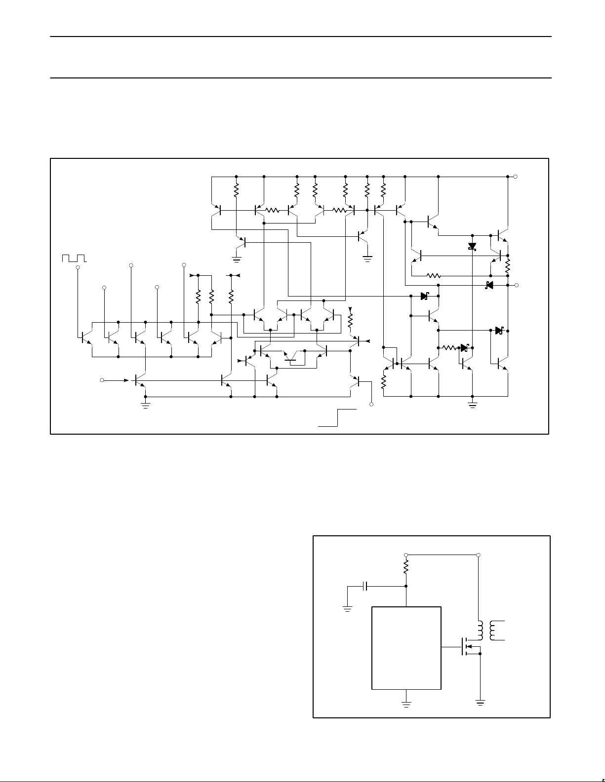
THE OUTPUT DRIVE STAGE
The output stage contains the power NOR inhibit gate, invert logic
function, and source-sink drivers. The driver stage is capable of
sourcing and sinking 100mA at frequencies up to 600kHz. The
output transistors are Schottky clamped to prevent saturation and
the resultant switching delay due to stored charge. A 2.5Ω current
sense resistor in the emitter of Q419 serves to drive active clamp
Q427 when the output sources more than 200mA. This places a limit
on the peak current available during instantaneous charging of a
power MOS FET gate. This feature protects the output stage from
inadvertent catastrophic overload.
When sinking current, the output is clamped to a maximum of 1.4V .
Output swing for positive output is typically V
S
-1.9V at 100mA
sourcing. Rise time for a 2000pF load at Pin 19 is typically 160ns
with a fall time of 80ns.
The power NOR gate provides a fast response inhibit function to
shutdown the output in the event of a number of different fault
Page 22
Philips Semiconductors Product specification
NE/SE5562Switched-mode power supply control circuit
1994 Aug 31
22
conditions. All inputs are internal to the device and do not appear
directly on the external pins as is shown on Figure 37.
The additional flexibility of an invert control allows the polarity at the
output during duty cycle to be reversed. This provides a simple
means of designing with P-channel power MOS FETs without adding
external inverters. The invert logic is controlled by a simple logic
signal at Pin 15. Grounding will cause the output to be a normal
positive output and a high level gives inverted output.
Q139
PWM
DEMAG
0.V
OUTPUT
LATCH
SHUT
DOWN
LATCH
START/STOP
LATCH
3.80V
R285kR295kR30
1.25k
1.5V
Q133
Q125
R31
10k
Q126
R32
3k
Q127
R33
5k
R34
5k
Q128
R35
3k
R30
15
Q129
Q131
R37
10k
R38
1k
Q132
Q155
Q130
Q154
17
+V
5
Q156
Q158
R39
300
Q157
R40
2.5
19
Q159
OUTPUT
Q165
Q165
Q164Q163
Q161
Q160
R43
4k
Q162
Q153
Q152
R42
1k
INVERT
NORM
15
Q150
OUTPUT NCR
Q149
Q140
Q148
Q145 Q146Q147
1.5V
Q138
Q137Q136Q135Q134
P
BIAS
R41
5k
Q151
Q143
Q144
V
ZQ142
Q141
SL00424
Figure 37. Output Driver Schematic
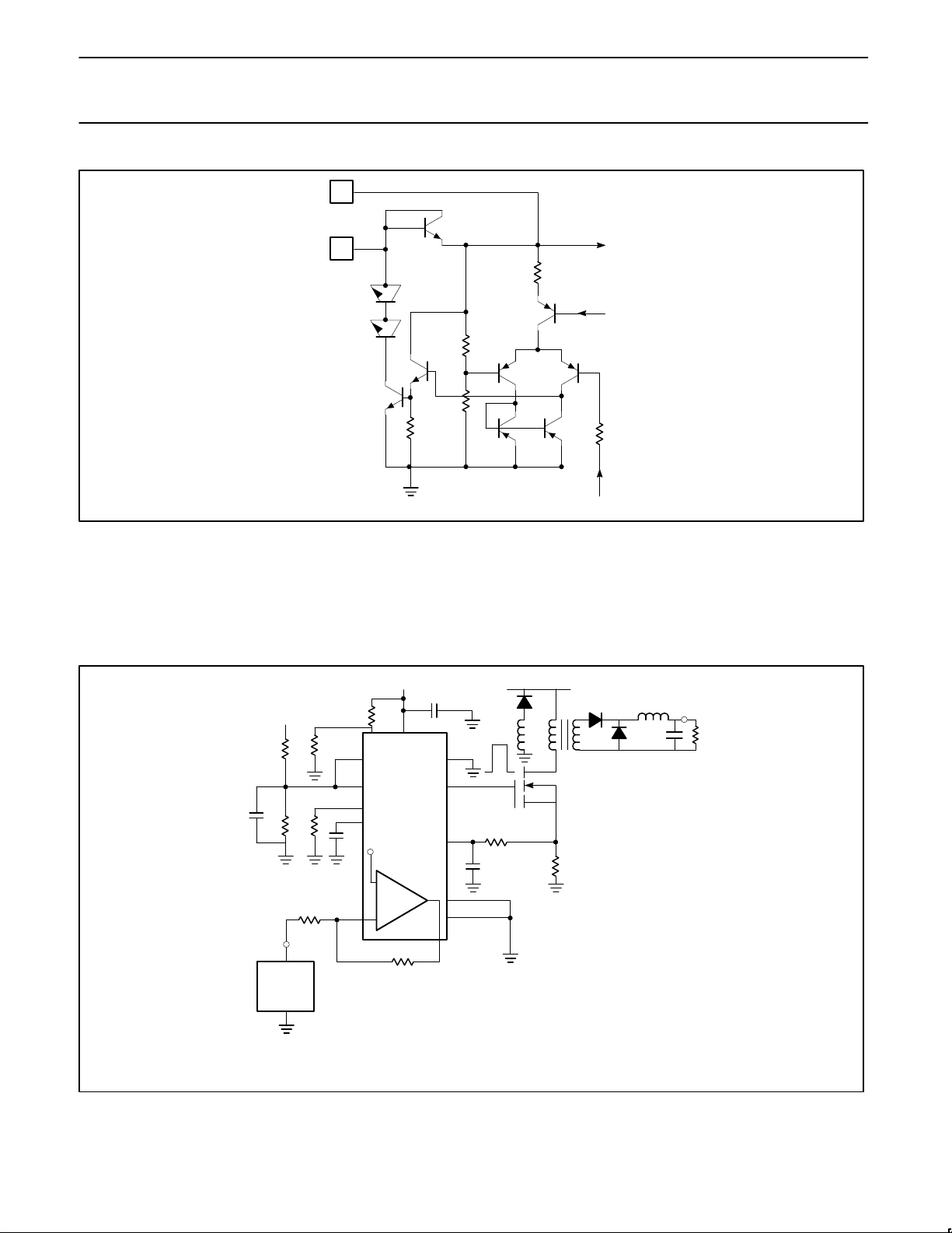
THE INTERNAL VOLTAGE REGULATOR
The internal regulator is configured to provide for external supply to
the NE/SE5562 from either a voltage feed or a current feed.
1
For the current-fed mode, a series-dropping resistor may be used to
power the device from voltages greater than 18V with current supply
of 15 to 25mA. Note that supply current stated in the data sheet is
for the device only without load on the output or V
Z
. Drive currents
also are pulse-related and thus reflect frequency components onto
the current-feed circuit. These must be filtered out at Pin 7 with
adequately large capacitors in order to prevent motor-boating (see
Figure 38 and Figure 39).
Input current to Pin 7 flows through Zeners Z
1
and Z2, and shunt
regulator transmitter QR. A differential amplifier with 3.80V reference
provides feedback to regulate V
S
to 15V.
In the voltage-fed mode using Pin 17, the Zeners prevent current
flow through QR for input voltages less than 19V .
Power dissipation of the device must stay within the allowable
package limits. These limits are derived from the thermal
characteristics of the particular package chosen. The NE5562N
plastic package is capable of operating within the temperature range
(ambient) of 0 to +70
°C. This rating applies to the surface-mount
product NE5562D also. Obviously, the power dissipation of the “D”
package is lower than the standard DIP. Thermal resistance for the
various packages are:
20-Pin plastic—NE5562N/SE5562N: θ
JA
61°C/W
20-Pin glass/ceramic—NE5562F/ SE5562F: θ
JA
90°C/W
20-Pin SO: -55 to +85°C/W (board-dependent)
NOTE:
1. See Figures 7 and 8 for internal Regulator Response Curves.
Design Example—An NE5562N is operated at 40°C ambient in the
voltage-fed mode with V
S
=15V; assume IS=22mA average:
++V
19
7
20
NE/SE5562
+
35V
47-100µF
SL00425
Figure 38. Current-Feed
Page 23
Philips Semiconductors Product specification
NE/SE5562Switched-mode power supply control circuit
1994 Aug 31
23
17
7
VOLTAGE
SOURCE
CURRENT
SOURCE
FROM BIASING
NETWORK
REGULATOR
790
30k
10k
20k
3.80V
V
S
Q
R
V
S
V
I
SL00426
Figure 39. Internal Voltage Regulator
∴ P
D
= (22×10-3) (15)
=330mW
Solving for the temperature rise from ambient to the IC functions:
Temperature rise = 61°C/W×0.33W
= 20.1°C
Junction temperatures will be 20.1°C above average ambient
temperatures which is 40°C
T
J
=40°C 20.1°C 60.1°C
The allowable maximum junction temperature is 150°C 125°C is
more conservative. The conditions of this example are safe.
NOTES:
1. Supply will become active as point ‘A’ reaches the level of V
REF
, 3.80V.
2. Monitor Pin 19 and Pin 2 on dual-trace scope with voltmeter connected to supply output.
ERROR
AMP
VARIABLE
SUPPLY
0-5V
V
Z
(0.472) V
Z
1µF
4
5
3
2
12 17
15
19
14
6
20
10
8
10k
10k
+12–15V
+25V
L
O
C
O
C
L
10k
‘A’
NE5562
10k
V
REF
R
SH
IRF530
1k
100pF
SL00427
Figure 40. Open-Loop Test Setup
Page 24
Philips Semiconductors Product specification
NE/SE5562Switched-mode power supply control circuit
1994 Aug 31
24
+
NOTE:
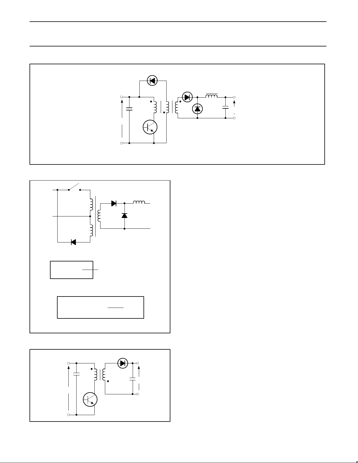
The P1 clamp winding prevents collector voltage from exceeding 2X VIN during off time.
L
O
D
2
C
O
D
3
S
1
C
P
V
IN
P
2
P
1
nn
Q
1
V
O
+
–
–
SL00428
Figure 41. Forward Converter
V
CEmax
+ V
imax
X
m ) n
m
(V)
max
t 1 *
m
m ) n
if m = n δ
max
< .5
Demagnetization of Core
Maximum Voltage Across Transistor
To Prevent Core Saturation Due to
Flux Staircasing
1
n
m
+
–
SL00429
Figure 42. Forward Converter Design Formulas
D
1
+
–
+
–
C
P
C
O
Q
1
V
O
V
I
SL00430
Figure 43. Isolated Secondary
Flyback Converter Design
Flyback Converter
Advantages:
•Simple circuit. Only one inductive component even with line isola-
tion.
•Economic. Low component count, low cost.
•Work over large input voltage variations.
•Can accommodate multiple outputs.
Disadvantages:
•Large output ripple current due to discontinuous energy transfer.
•Large output capacitor; has to supply part of the load current.
•Low leakage inductance required to prevent high voltage spikes at
the switching transistors.
•Relatively large core volume for the output power. Core driven in
one direction only.
Design Parameters for Flyback Inductor
Input
•Minimum input voltage
•Maximum input voltage
Output
•Output voltage or voltages
•Output current or currents
•Output load
Page 25
Philips Semiconductors Product specification
NE/SE5562Switched-mode power supply control circuit
1994 Aug 31
25
Frequency of Operation
Estimate of Overall Efficiency. (η)
2N3906
220k
10k
(PIN 9)
7.50V
5.1k
13k
3.26V
570
pF
3
2
4
5
6
8
OFF
+5V
0V
REMOTE
SHUT DOWN
+5
SENSE
1.3k
1k
F. FWD
SENSE
40k
CLOCK
DELAY
LOW
SUPPLY
DETECTOR
PWM
L
A
T
C
H
D
R
I
V
E
R
START/
STOP
INVERT
3.80V
ERROR
AMP
+
–
10 20 16
OC1 OC2
SHUT
DOWN
PGM
LA645V
CL
1
CL
2
PIN
14
1.6k
AUXILIARY
BOOTSTRAP
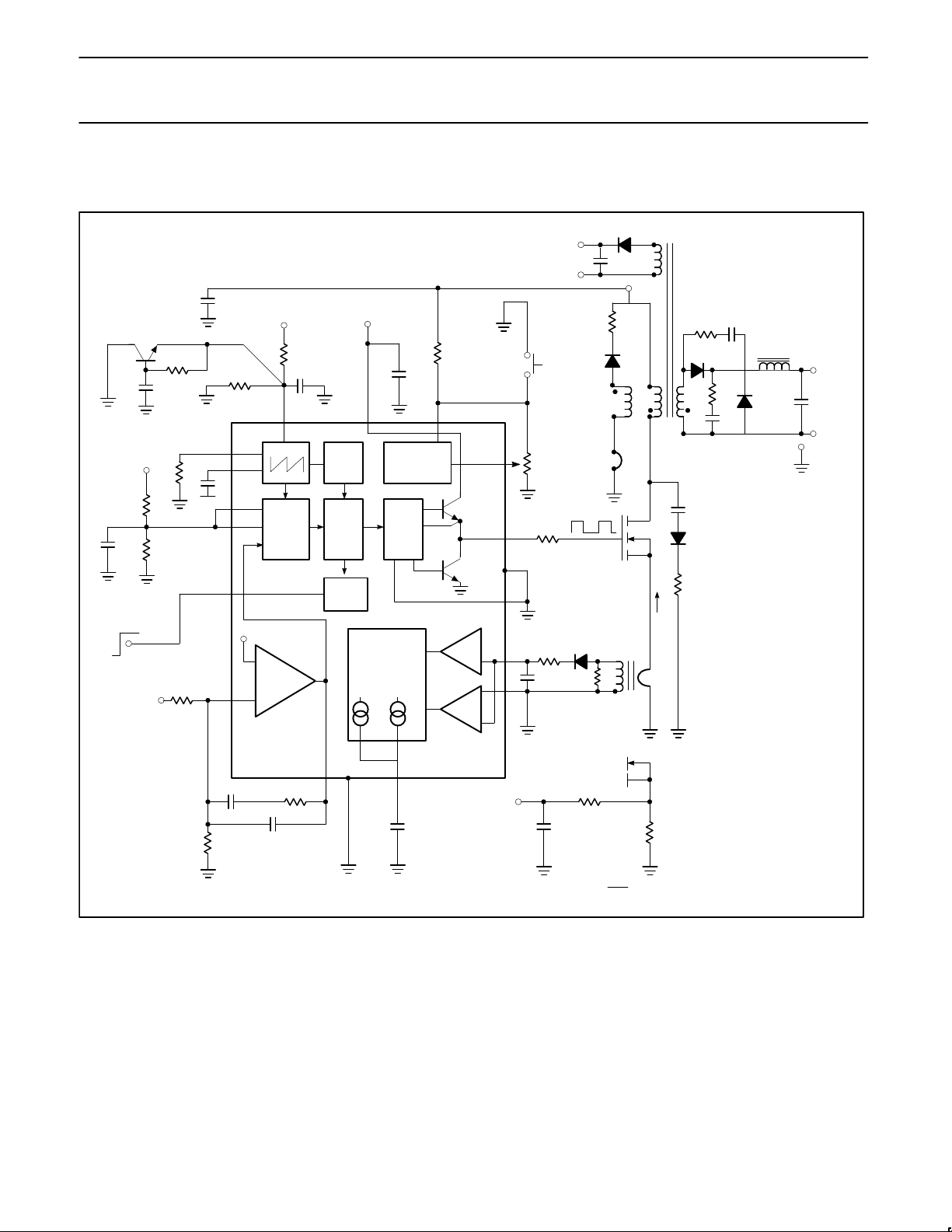
SUPPLY
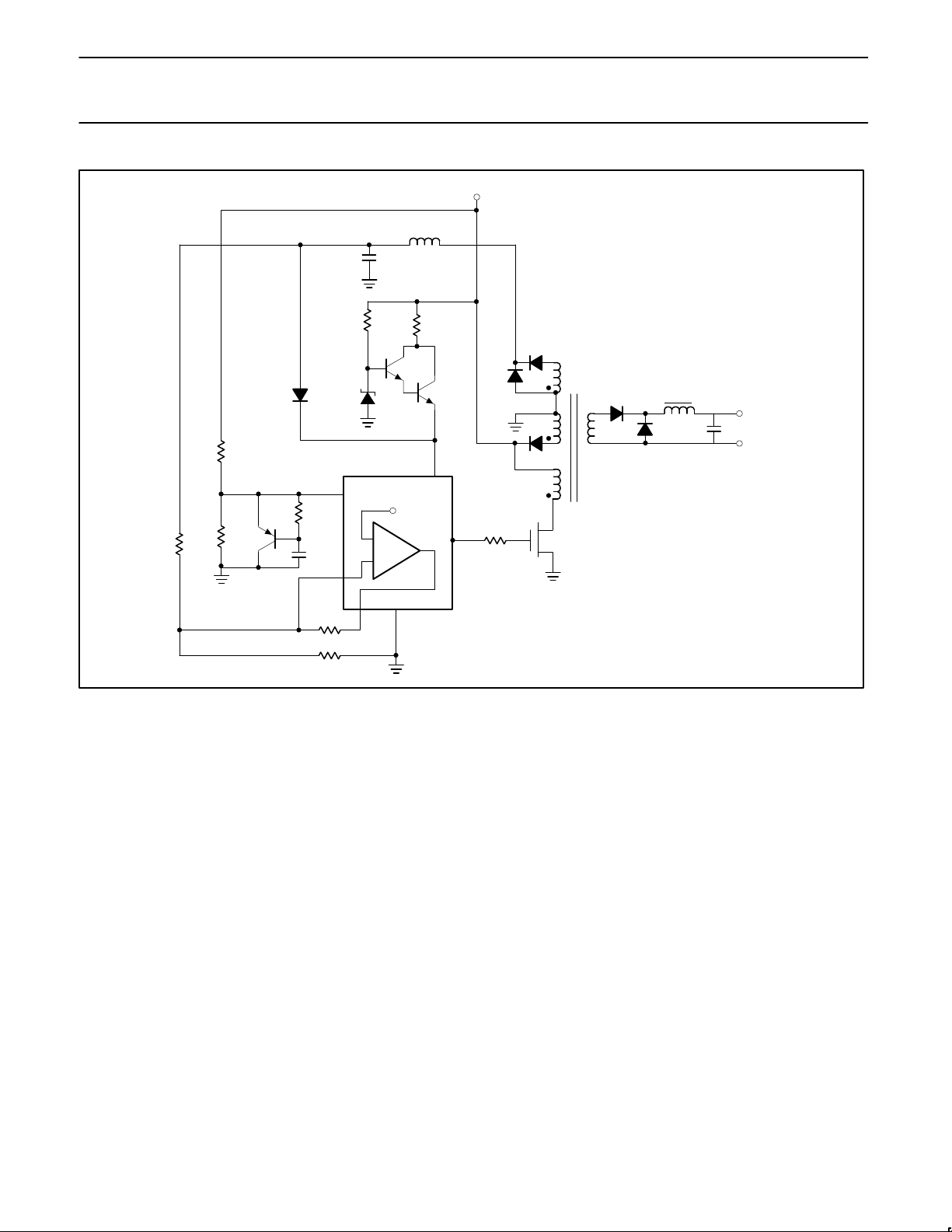
(SEE FIGURE 43)
+16V
+V=48V
10
BYV26C
RESET
[O.C.]
n n
HYSTERESIS
ADJUST
13
19
18
15
14
100pF
IN914
PIN
14
ALTERNATE
CIRCUIT
0.24
BUZ41A
4.7nF
BYV26C
10
4.7
3.9
BYV19-35
3.9
+5V
COM.
Q
1
R
SH
0.00µF
V
OUT
Q
1
D
1
D
2
D
3
0.01µF
L
0
+V
OUT
I
CC
T
2
0.01µF
T
1
1
I
MAX
+
0.53
R
SH
C @ T
100:1
ON
C
SS
10k
V
Z
0.47µF
+V
S
= 12V
0.01µF
1 17
12
C
3
0.22µF
C
DELAY
13µA 550µA
SL00431
Figure 44. Forward Converter, 100W – 5V
Page 26
Philips Semiconductors Product specification
NE/SE5562Switched-mode power supply control circuit
1994 Aug 31
26
+48V
+17V
100
15V
D40K2
7
1
8
10
20
19
+3.80V
+
–
n
n/2
+5V
220k
6.8k
33k
n
P
3
P
2
P
1
R
F
NE/SE5562
n
+V
O
0.22µF
SL00432
Figure 45. Shunt-Regulated Output With Bootstrap Supply
Page 27
Philips Semiconductors Product specification
NE/SE5562Switched-mode power supply control circuit
1994 Aug 31
27
NOTES:
a. Unlimited choke current
b. Interrupted choke current
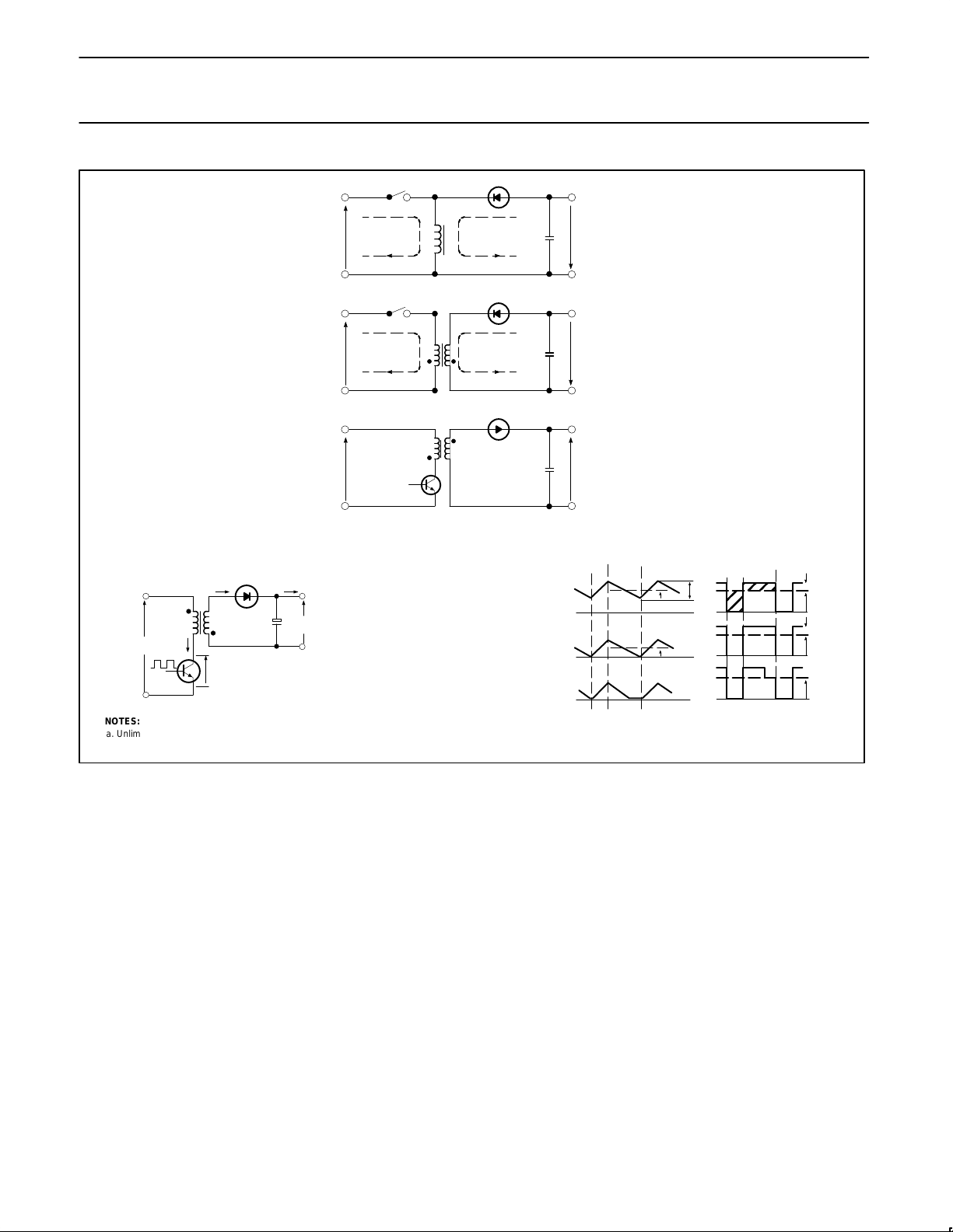
Development of Practical Flyback Converter Circuit
Flyback Converter and Current and Voltage Waveforms
a
b
c
O T T
TR1 ON OFF
i
L
i
L
i
L
I
L
I
L
V
CE
V
CE
V
CE
i
L
i
L
nV
O
V
I
nV
O
V
I
V
I
δ
O T T
δ
V
I
V
O
C
O
V
CE
TR1
I
C
I
O
I
D1
L1
D1
T1
N1
+
Negative Output
Positive Output
CURRENT PATH
WITH SWITCH
CLOSED
CURRENT PATH
WITH SWITCH
OPEN
CURRENT PATH
WITH SWITCH
OPEN
CURRENT PATH
WITH SWITCH
CLOSED
V
O
V
I
V
O
V
I
V
O
V
I
S
S
+
–
+
–
+
–
+
–
+
–
+
SL00433
Figure 46.
Page 28
Philips Semiconductors Product specification
NE/SE5562Switched-mode power supply control circuit
1994 Aug 31
28
NOTE:
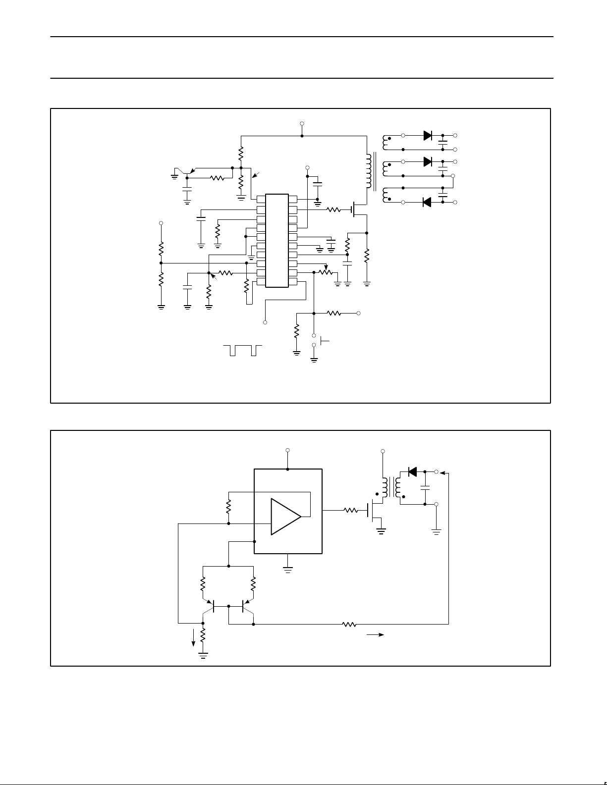
400kHz operation with feed-forward line regulation and cycle-by-cycle current timing.
2N3906
220k
6.8k
33k
FEEDFORWARD
+12V
CERAMIC
T
BUZ41A
+5V
COM
+12
COM
–12
4.7
O.C.
HYST.
100pF
LOW
SUPPLY
SENSE
RESET
+5
0V–
EXT
SYNC
1
2
3
4
5
6
7
8
9
10
20
19
18
17
16
15
14
13
12
11
3.5V
3.8V
+5V
1k
NE5562
5.1k
570pF
0.22µF
0.1µF
V
0’
SENSE
R
1
R
2
C
SS
C
T
R
T
R
F
R
SH
+V
S
48V +V
S
C
DELAY
SL00434
Figure 47. NE5562 Flyback Converter
–V
OUT
(17)
(10)
(8)
+
–
ERROR
AMP
(19)
(20)
+7.50V
(9)
100
100
2N3906
+3.80V
++V
R
S
I
S
R
I
IS’
V
Z
R
F
SL00435
Figure 48. Negative Output Regulator Using Current Mirror
Page 29
Philips Semiconductors Product specification
NE/SE5562Switched-mode power supply control circuit
1994 Aug 31
29
+15V
–15V
+15V
17
4
+
–
PWM
NE5018
D/A
NE/SE5562
1–5V
+5V
–12V
NE5034
A/D
15
5k
+
PROGRAMMED
SUPPLY
VOLTAGE
+
(–)
SLAVED
OUTPUTS
(+)
+48V
µP
SL00436
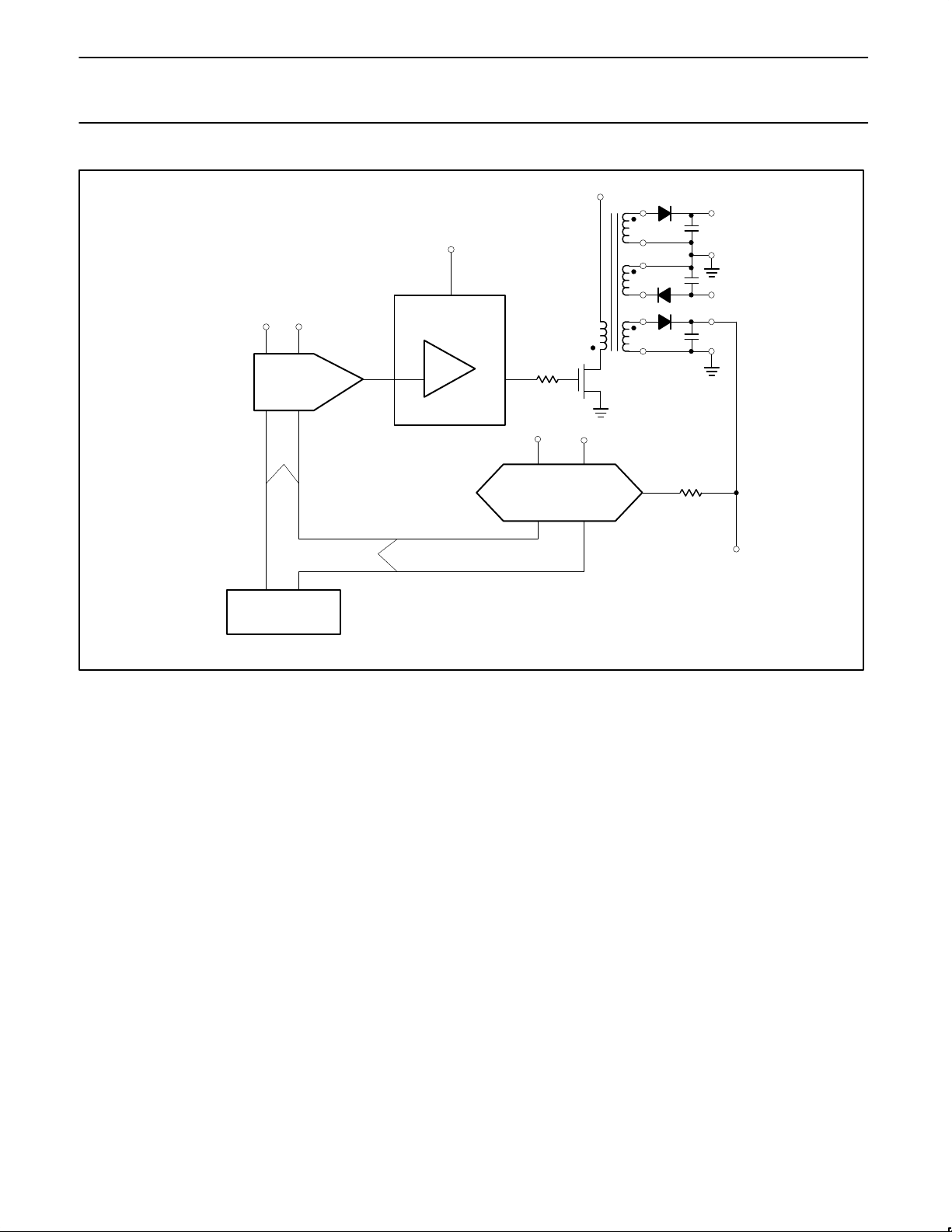
Figure 49. Microprocessor Controlled SMPS
REFERENCES
1. R.D. Middlebrook and Slobadan Cuk, Advances in Switched
Mode Power Conversion, Volumes I and II, TESLA Co., Pasadena, CA, 1983.
2. Rudolf P. Stevens and Gordon E. Bloom, Modern DC to DC
Switchmode Power Convertor Circuits, Van Nostrand Reinhold/
Computer Science and Engineering Series, 1985.
3. H. Dean Venable, Stability Analysis Made Simple, Venable
Industries, Inc., 1981.
4. J. Jongsma and L.P.M. Bracke, High Frequency Ferrite Power
Transformer and Choke Design, N. V. Philips ELCOMA Publications, Eindhoven, the Netherlands, September 1982.
5. Edwin S. Oxner, Power FETs and Their Applications, Prentice-
Hall, 1982.
 Loading...