

Page 1
INTEGRATED CIRCUITS
NE/SA/SE5532/5532A
Internally-compensated dual low noise
operational amplifier
Product specification 1997 Sept 29
IC11 Data Handbook
Page 2
Philips Semiconductors Product specification
Internally-compensated dual low noise
operational amplifier
DESCRIPTION
The 5532 is a dual high-performance low noise operational amplifier.
Compared to most of the standard operational amplifiers, such as
the 1458, it shows better noise performance, improved output drive
capability and considerably higher small-signal and power
bandwidths.
This makes the device especially suitable for application in
high-quality and professional audio equipment, instrumentation and
control circuits, and telephone channel amplifiers. The op amp is
internally compensated for gains equal to one. If very low noise is of
prime importance, it is recommended that the 5532A version be
used because it has guaranteed noise voltage specifications.
FEA TURES
•Small-signal bandwidth: 10MHz
•Output drive capability: 600Ω, 10V
•Input noise voltage:
5nV Hz
•DC voltage gain: 50000
•AC voltage gain: 2200 at 10kHz
•Power bandwidth: 140kHz
•Slew rate: 9V/µs
•Large supply voltage range: ±3 to ±20V
•Compensated for unity gain
RMS
(typical)
NE/SA/SE5532/5532A
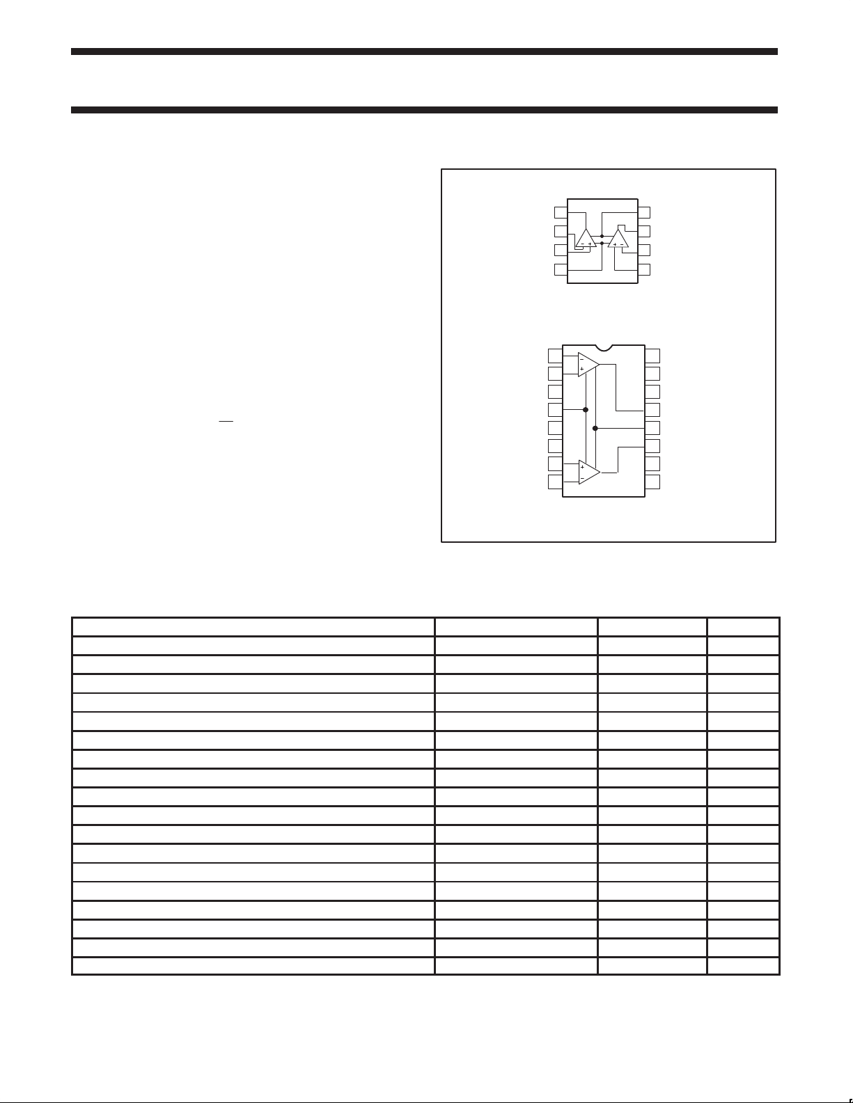
PIN CONFIGURATIONS
FE, N, D8 Packages
OUTPUT A
INVERTING INPUT A
NON-INVERTING INPUT A
NOTE:
1. SOL and non-standard pinout.
1
2
3
V-
TOP VIEW
D Package
–IN
1
A
2
+IN
A
3
NC
4
–V
CC
5
NC
6
NC
7
+IN
B
8
–IN
B
TOP VIEW
Figure 1. Pin Configurations
8
V+
7
B
6
54
1
16
15
14
13
12
11
10
9
OUTPUT B
INVERTING INPUT B
NON-INVERTING INPUT B
NC
NC
NC
OUT
A
+V
CC
OUT
B
NC
NC
SL00332
A
ORDERING INFORMATION
DESCRIPTION TEMPERATURE RANGE ORDER CODE DWG #
8-Pin Plastic Dual In-Line Package (DIP) 0 to 70°C NE5532N SOT97-1
8-Pin Plastic Dual In-Line Package (DIP) –40°C to +85°C SA5532N SOT97-1
8-Pin Plastic Dual In-Line Package (DIP) –40°C to +85°C SA5532AN SOT97-1
8-Pin Ceramic Dual In-Line Package (CERDIP) 0 to 70°C NE5532FE 0580A
8-Pin Plastic Dual In-Line Package (DIP) 0 to 70°C NE5532AN SOT97-1
8-Pin Ceramic Dual In-Line Package (CERDIP) 0 to 70°C NE5532AF 0580A
8-Pin Ceramic Dual In-Line Package (CERDIP) -55°C to +125°C SE5532FE 0580A
8-Pin Ceramic Dual In-Line Package (CERDIP) -55°C to +125°C SE5532AF 0580A
8-Pin Small Outline Package (SO) 0 to 70°C NE5532AD8 SOT96-1
8-Pin Small Outline Package (SO) –40°C to 85°C SA5532D8 SOT96-1
8-Pin Small Outline Package (SO) –40°C to 85°C SA5532AD8 SOT96-1
8-Pin Small Outline Package (SO) -55°C to +125°C SE5532AD8 SOT96-1
8-Pin Small Outline Package (SO) 0 to 70°C NE5532D8 SOT96-1
8-Pin Small Outline Package (SO) –40°C to 85°C SA5532D8 SOT96-1
8-Pin Small Outline Package (SO) –40°C to 85°C SA5532AD8 SOT96-1
8-Pin Small Outline Package (SO) -55°C to +125°C SE5532D8 SOT96-1
16-Pin Plastic Small Outline Large (SOL) Package 0 to 70°C NE5532D SOT162-1
16-Pin Plastic Dual In-Line Package (DIP) -55°C to +125°C SE5532N SOT38-4
1997 Sept 29 853-0949 16639
2
Page 3
Philips Semiconductors Product specification
Internally-compensated dual low noise
operational amplifier
EQUIVALENT SCHEMATIC (EACH AMPLIFIER)
+
_
NE/SA/SE5532/5532A
SL00333
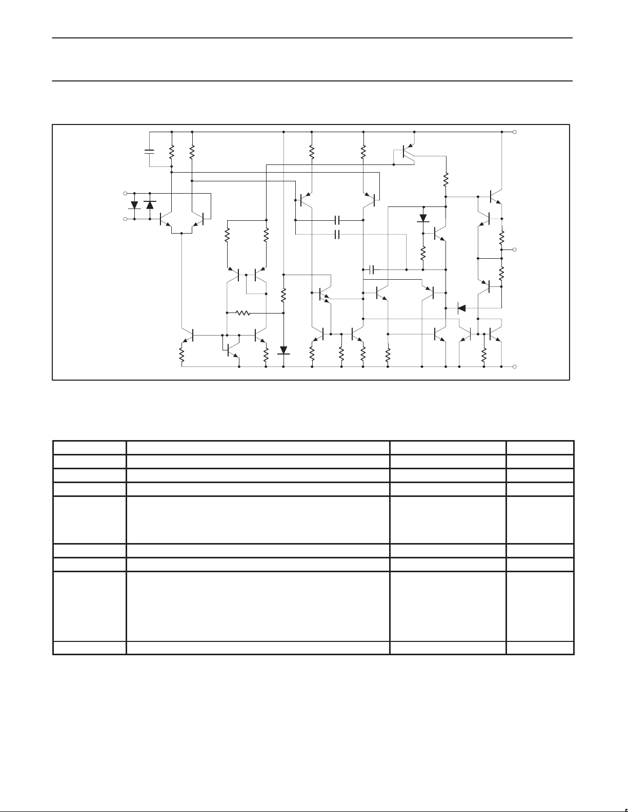
Figure 2. Equivalent Schematic (Each Amplifier)
ABSOLUTE MAXIMUM RATINGS
SYMBOL PARAMETER RATING UNIT
V
S
V
IN
V
DIFF
T
A
T
STG
T
J
P
D
T
SOLD
NOTES:
1. Diodes protect the inputs against over-voltage. Therefore, unless current-limiting resistors are used, large currents will flow if the differential
input voltage exceeds 0.6V . Maximum current should be limited to ±10mA.
2. Thermal resistances of the above packages are as follows:
N package at 100°C/W
F package at 135°C/W
D package at 105°C/W
D8 package at 160°C/W
Supply voltage ±22 V
Input voltage ±V
Differential input voltage
1
SUPPLY
±0.5 V
Operating temperature range
SA5532/A –40 to +85 °C
NE5532/A 0 to 70 °C
SE5532/A -55 to +125 °C
Storage temperature -65 to +150 °C
Junction temperature 150 °C
Maximum power dissipation,
TA=25°C (still-air)
2
8 D8 package 780 mW
8 N package 1200 mW
8 FE package 1000 mW
16 D package 1200 mW
Lead soldering temperature (10sec max) 300 °C
V
1997 Sept 29
3
Page 4
Philips Semiconductors Product specification
SYMBOL
PARAMETER
TEST CONDITIONS
UNIT
A
VOL
Large-signal voltage gain
V
OUT
Out ut swing
V
SYMBOL
PARAMETER
TEST CONDITIONS
UNIT
Internally-compensated dual low noise
operational amplifier
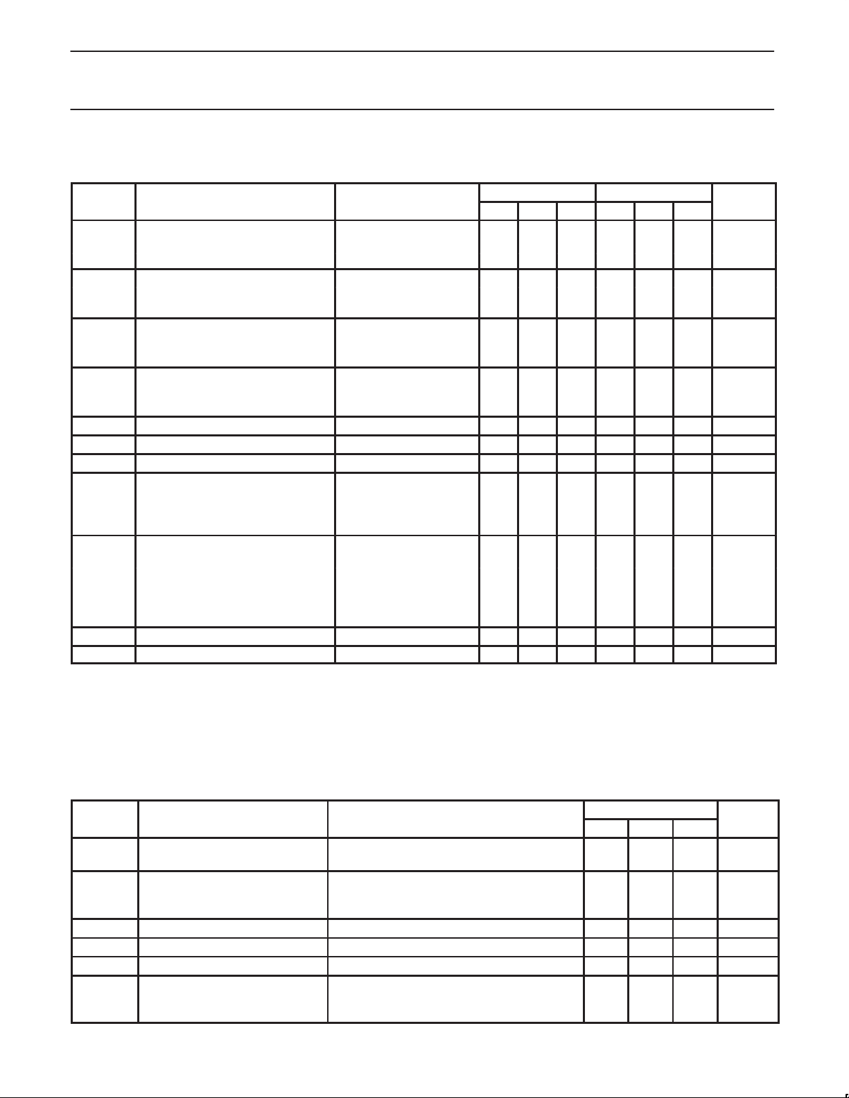
DC ELECTRICAL CHARACTERISTICS
TA=25°C VS=±15V, unless otherwise specified.
V
OS
∆VOS/∆T 5 5 µV/°C
I
OS
∆IOS/∆T 200 200 pA/°C
I
B
∆IB/∆T 5 5 nA/°C
I
CC
V
CM
CMRR Common-mode rejection ratio 80 100 70 100 dB
PSRR Power supply rejection ratio 10 50 10 100 µV/V
R
IN
I
SC
NOTES:
1. Diodes protect the inputs against overvoltage. Therefore, unless current-limiting resistors are used, large currents will flow if the differential
input voltage exceeds 0.6V . Maximum current should be limited to ±10mA.
2. For operation at elevated temperature, derate packages based on the package thermal resistance.
3. Output may be shorted to ground at V
not exceeded.
Offset voltage 0.5 2 0.5 4 mV
Offset current 100 10 150 nA
Input current 200 400 200 800 nA
Supply current
Common-mode input range ±12 ±13 ±12 ±13 V
-
p
Input resistance 30 300 30 300 kΩ
Output short circuit current 10 38 60 10 38 60 mA
1, 2, 3
SE/5532/5532A NE/SA/5532/5532A
Min Typ Max Min Typ Max
Over temperature 3 5 mV
Over temperature 200 200 nA
Over temperature 700 1000 nA
Over temperature 13 mA
RL≥2kΩ, VO=±10V 50 100 25 100 V/mV
Over temperature 25 15 V/mV
RL≥600Ω, VO=±10V 40 50 15 50 V/mV
Over temperature 20 10 V/mV
RL≥600Ω ±12 ±13 ±12 ±13
Over temperature ±10 ±12 ±10 ±12
RL≥600Ω, VS=±18V ±15 ±16 ±15 ±16
Over temperature ±12 ±14 ±12 ±14
RL≥2kΩ ±13 ±13.5 ±13 ±13.5
Over temperature ±12 ±12.5 ±10 ±12.5
=±15V, TA=25°C Temperature and/or supply voltages must be limited to ensure dissipation rating is
S
NE/SA/SE5532/5532A
8 10.5 8 16 mA
AC ELECTRICAL CHARACTERISTICS
TA=25°C VS=±15V, unless otherwise specified.
R
OUT
A
V
GBW Gain bandwidth product CL=100pF, RL=600Ω 10 MHz
SR Slew rate 9 V/µs
1997 Sept 29
NE/SA/SE5532/5532A
Min Typ Max
Output resistance
AV=30dB Closed-loop
f=10kHz, R
=600Ω
L
0.3 Ω
Voltage-follower
Overshoot VIN=100mV
P-P
10 %
CL=100pF, RL=600Ω
Gain f=10kHz 2.2 V/mV
V
=±10V 140 kHz
Power bandwidth V
OUT
=±14V, RL=600Ω, 100 kHz
OUT
VCC=±18V
4
Page 5
Philips Semiconductors Product specification
SYMBOL
PARAMETER
TEST CONDITIONS
UNIT
Internally-compensated dual low noise
operational amplifier
ELECTRICAL CHARACTERISTICS
TA=25°C VS=±15V, unless otherwise specified.
V
NOISE
I
NOISE
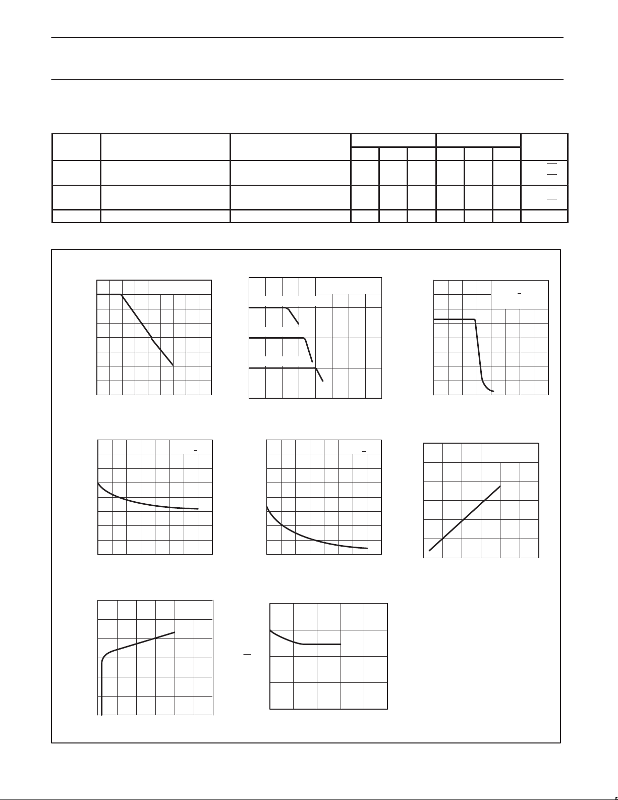
TYPICAL PERFORMANCE CHARACTERISTICS
Input noise voltage fO=30Hz 8 8 12 nV/√Hz
Input noise current fO=30Hz 2.7 2.7 pA/√Hz
Channel separation f=1kHz, RS=5kΩ 110 110 dB
Open-Loop Frequency
Response
120
80
40
GAIN (dB)
0
TYPICAL VALUES
60
40
20
GAIN (dB)
Closed-Loop Frequency
RF = 10kΩ; RE = 100Ω
RF = 9kΩ; RE = 1kΩ
RF = 1kΩ; RE = ∞
0
NE/SA/SE5532/5532A
NE/SE5532 NE/SA/SE5532A
Min Typ Max Min Typ Max
fO=1kHz 5 5 6 nV/√Hz
fO=1kHz 0.7 0.7 pA/√Hz
Response
TYPICAL VALUES
(V)
Vo(p-p)
Large-Signal Frequency
Response
40
VS = +15V
TYPICAL VALUES
30
20
10
-40
2103104105106107
10 10
f (Hz)
-20
3104105106107108
10
f (Hz)
Output Short-Circuit Current Input Bias Current
80
60
I
O
40
(mA)
20
0
-55 -25 0 25 50 75 100 +125 -55 -25 0 25 50 75 100 +125
(oC)
T
A
TYP
V
S
= +15V
Supply Current
6
IO = 0
TYP
I
P
I
N
(mA)
4
2
(nV
I
(mA)
1,4
1,2
I
0,8
0,4
0
Input Noise Voltage Density
–2
10
10
1
Hz
)
–1
10
TYP
TA (oC)
V
S
= +15V
0
2103104105106107
10
f (Hz)
Input Commom-Mode
Voltage Range
30
20
(V)
V
IN
10
0
01020
Vp; -V
(V)
N
TYPICAL VALUES
1997 Sept 29
0
0 10 20
Vp; -VN (V)
–2
10
10 10210310
4
f (Hz)
Figure 3. Typical Performance Characteristics
5
SL00334
Page 6
Philips Semiconductors Product specification
Internally-compensated dual low noise
operational amplifier
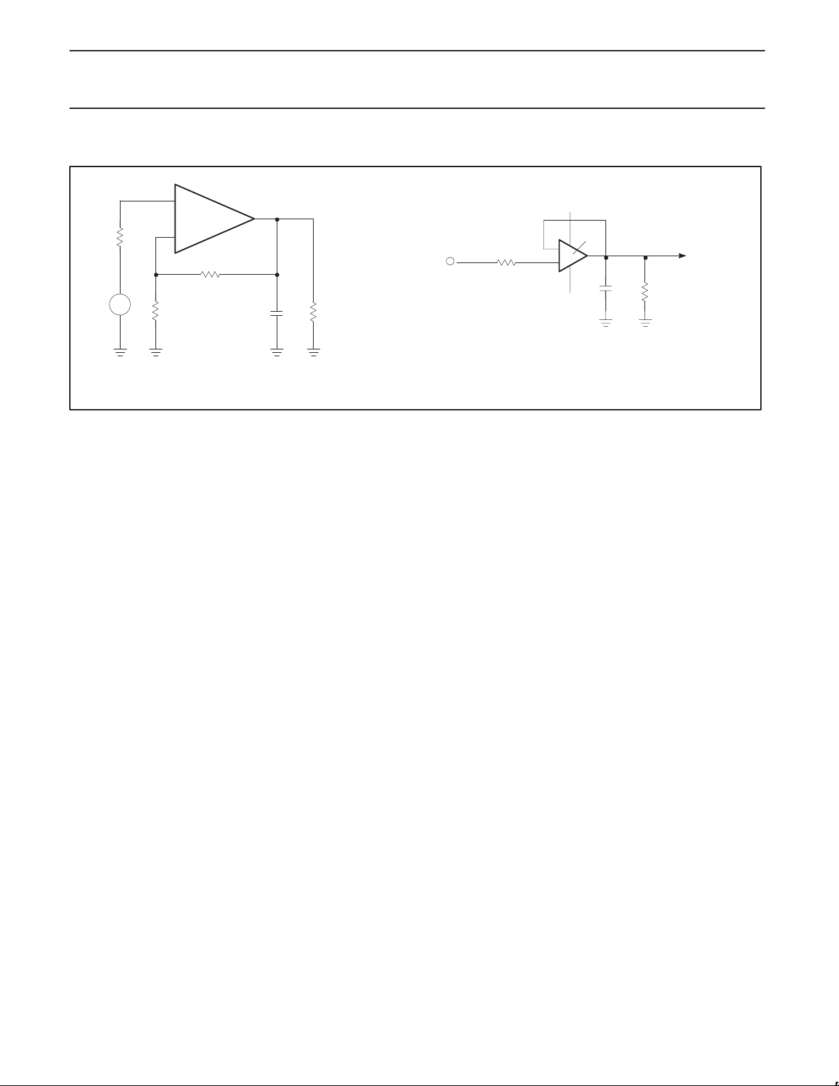
TEST CIRCUITS
+
R
E
5532 (1/2)
–
R
F
100pF
800Ω
Figure 4. Test Circuits
R
S
25Ω
V
I
Closed-Loop Frequency Response
NE/SA/SE5532/5532A
V+
5532
V
IN
1k
–
+
100pF
V–
Voltage-Follower
600Ω
V
OUT
SL00335
1997 Sept 29
6
Page 7
Philips Semiconductors Product specification
Internally-compensated dual low noise operational
amplifier
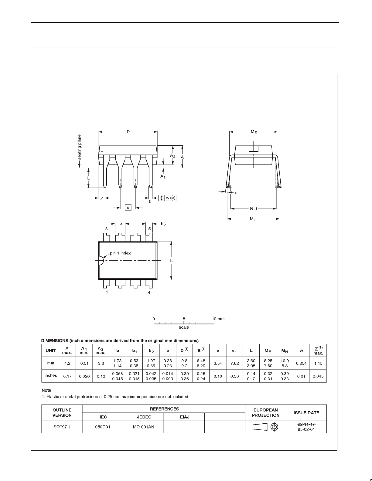
DIP8: plastic dual in-line package; 8 leads (300 mil) SOT97-1
NE/SA/SE5532/5532A
1997 Sept 29
7
Page 8
Philips Semiconductors Product specification
Internally-compensated dual low noise operational
amplifier
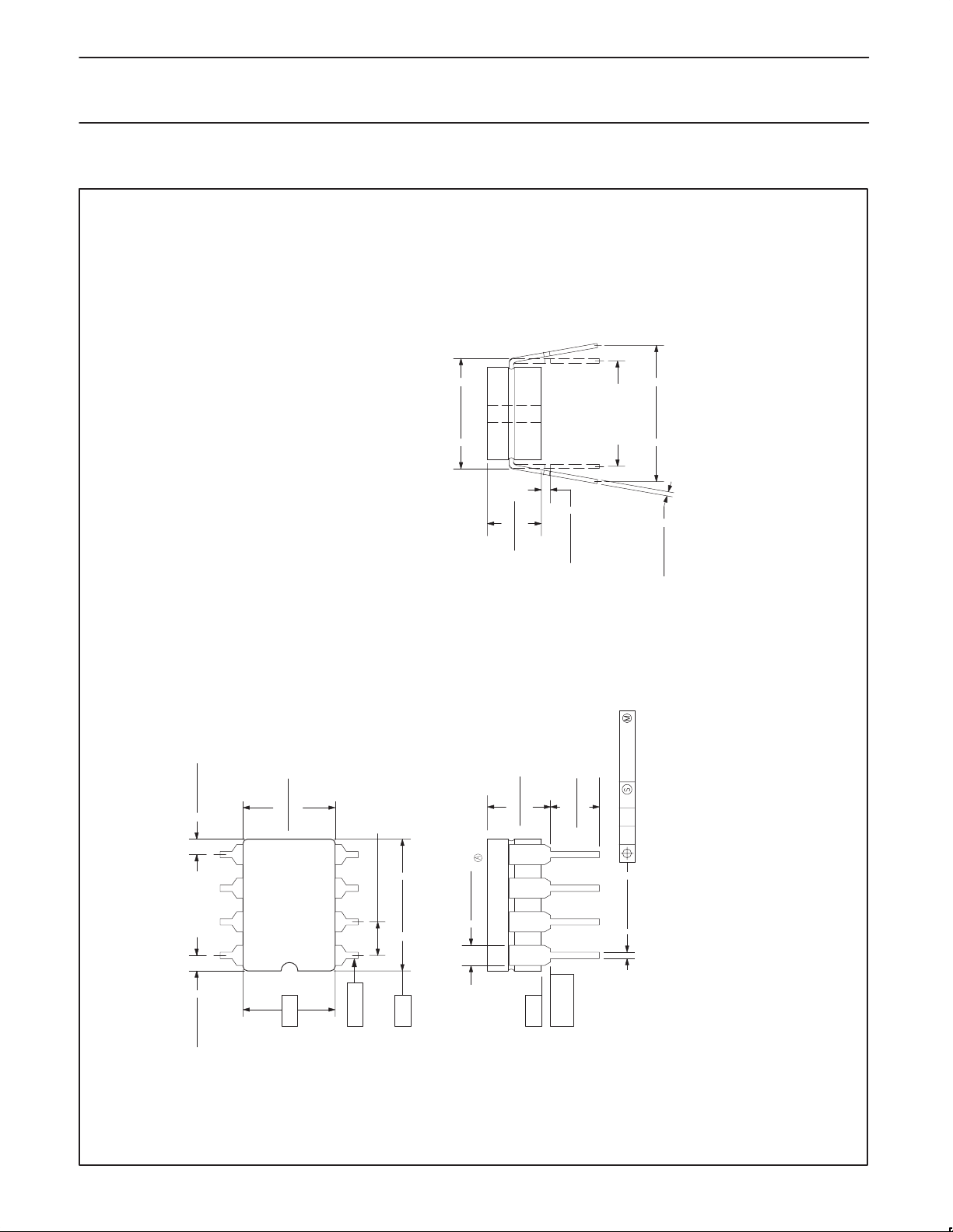
0580A 8-PIN (300 mils wide) CERAMIC DUAL IN-LINE (F) PACKAGE
(NOTE 4)
0.320 (8.13)
0.290 (7.37)
NE/SA/SE5532/5532A
BSC
(NOTE 4)
0.395 (10.03)
0.300 (7.62)
0.300 (7.62)
and include allowance for glass overrun and meniscus
on the seal line, and lid to base mismatch.
constrained to be perpendicular to plane T.
shown in parentheses.
NOTES:
1. Controlling dimension: Inches. Millimeters are
2. Dimension and tolerancing per ANSI Y14. 5M-1982.
3. “T”, “D”, and “E” are reference datums on the body
0.055 (1.40)
0.030 (0.76)
0.303 (7.70)
0.245 (6.22)
counterclockwise to Pin #8 when viewed
from the top.
4. These dimensions measured with the leads
5. Pin numbers start with Pin #1 and continue
0.100 (2.54) BSC
0.408 (10.36)
0.376 (9.55)
0.070 (1.78)
0.050 (1.27)
0.175 (4.45)
0.145 (3.68)
0.200 (5.08)
0.165 (4.19)
0.035 (0.89)
0.020 (0.51)
0.165 (4.19)
0.125 (3.18)
0.015 (0.38)
0.010 (0.254)TED
0.023 (0.58)
0.015 (0.38)
0.010 (0.25)
853–0580A 006688
1997 Sept 29
0.055 (1.40)
0.030 (0.76)
– E –
PIN # 1
– D –
PLANE
SEATING
– T –
8
Page 9
Philips Semiconductors Product specification
Internally-compensated dual low noise operational
amplifier
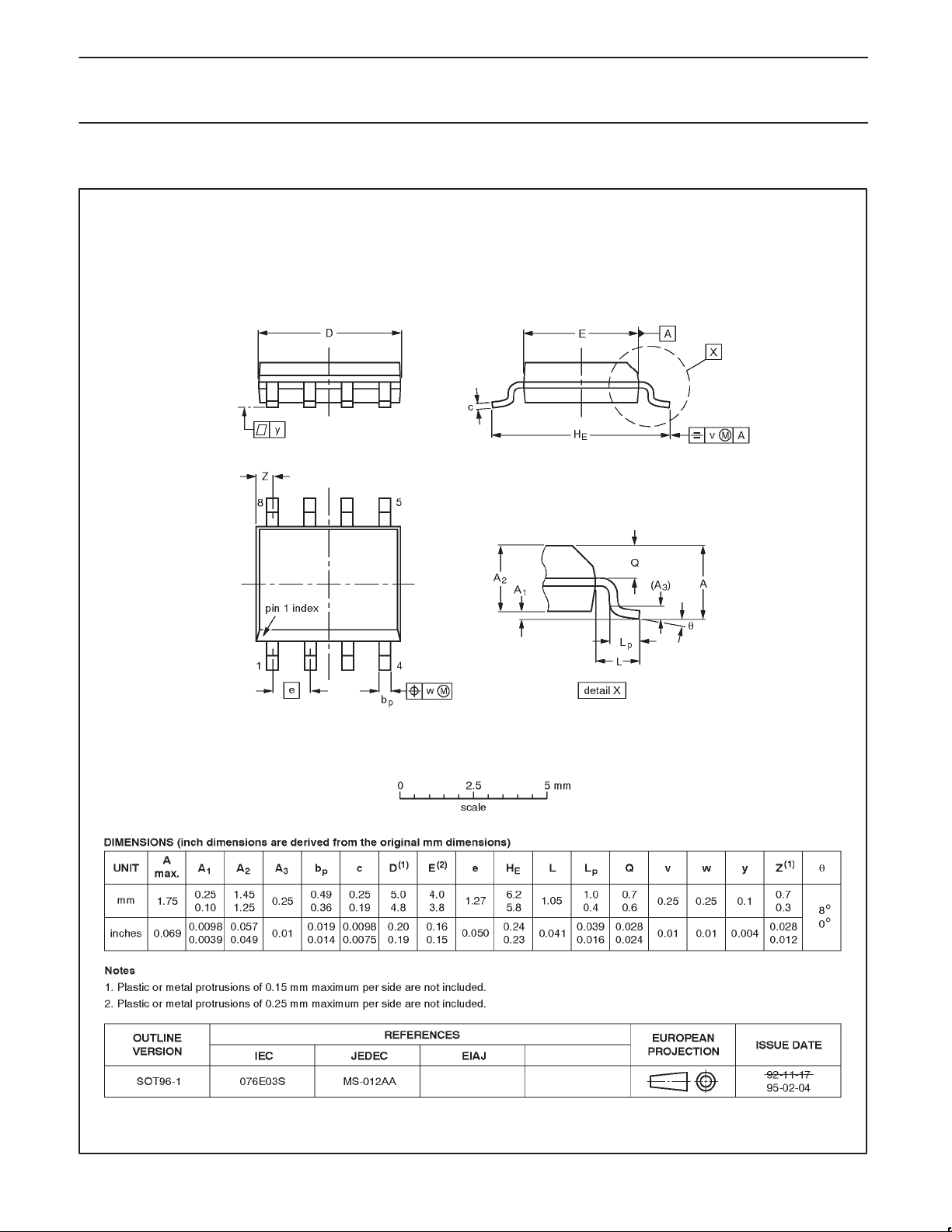
SO8: plastic small outline package; 8 leads; body width 3.9mm SOT96-1
NE/SA/SE5532/5532A
1997 Sept 29
9
Page 10
Philips Semiconductors Product specification
Internally-compensated dual low noise operational
amplifier
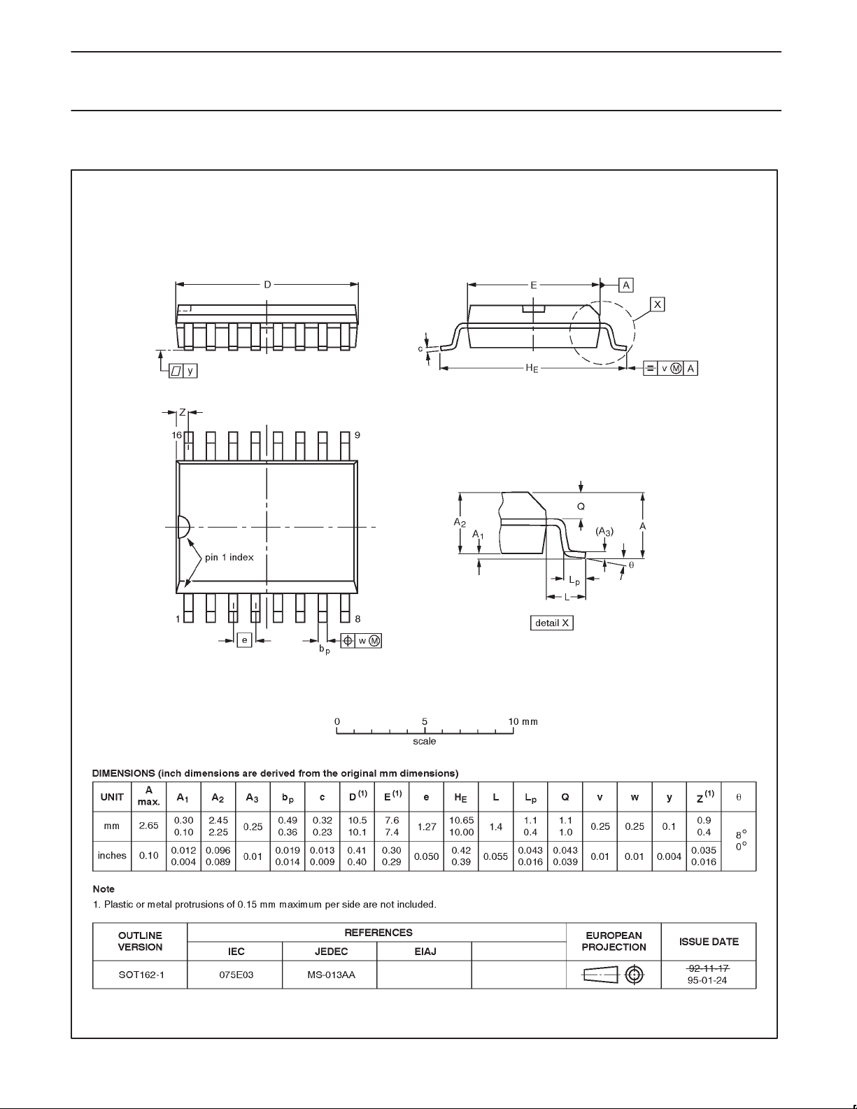
SO16: plastic small outline package; 16 leads; body width 7.5 mm SOT162-1
NE/SA/SE5532/5532A
1997 Sept 29
10
Page 11
Philips Semiconductors Product specification
Internally-compensated dual low noise operational
amplifier
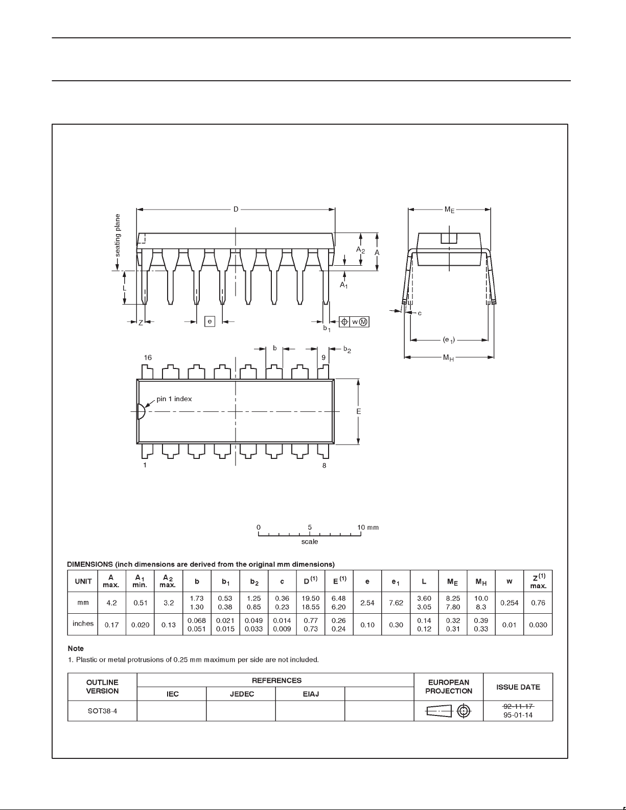
DIP16: plastic dual in-line package; 16 leads (300 mil) SOT38-4
NE/SA/SE5532/5532A
1997 Sept 29
11
Page 12

Philips Semiconductors Product specification
Internally-compensated dual low noise operational
amplifier
DEFINITIONS
NE/SA/SE5532/5532A
Data Sheet Identification Product Status Definition
Objective Specification
Preliminary Specification
Product Specification
Philips Semiconductors and Philips Electronics North America Corporation reserve the right to make changes, without notice, in the products,
including circuits, standard cells, and/or software, described or contained herein in order to improve design and/or performance. Philips
Semiconductors assumes no responsibility or liability for the use of any of these products, conveys no license or title under any patent, copyright,
or mask work right to these products, and makes no representations or warranties that these products are free from patent, copyright, or mask
work right infringement, unless otherwise specified. Applications that are described herein for any of these products are for illustrative purposes
only. Philips Semiconductors makes no representation or warranty that such applications will be suitable for the specified use without further testing
or modification.
LIFE SUPPORT APPLICA TIONS
Philips Semiconductors and Philips Electronics North America Corporation Products are not designed for use in life support appliances, devices,
or systems where malfunction of a Philips Semiconductors and Philips Electronics North America Corporation Product can reasonably be expected
to result in a personal injury. Philips Semiconductors and Philips Electronics North America Corporation customers using or selling Philips
Semiconductors and Philips Electronics North America Corporation Products for use in such applications do so at their own risk and agree to fully
indemnify Philips Semiconductors and Philips Electronics North America Corporation for any damages resulting from such improper use or sale.
Philips Semiconductors
811 East Arques Avenue
P.O. Box 3409
Sunnyvale, California 94088–3409
Telephone 800-234-7381
Formative or in Design
Preproduction Product
Full Production
This data sheet contains the design target or goal specifications for product development. Specifications
may change in any manner without notice.
This data sheet contains preliminary data, and supplementary data will be published at a later date. Philips
Semiconductors reserves the right to make changes at any time without notice in order to improve design
and supply the best possible product.
This data sheet contains Final Specifications. Philips Semiconductors reserves the right to make changes
at any time without notice, in order to improve design and supply the best possible product.
Copyright Philips Electronics North America Corporation 1997
print code Date of release: 04–96
Document order number: 9397 750 01699
All rights reserved. Printed in U.S.A.
1997 Sept 29
12
 Loading...