

Page 1
Philips Semiconductors Linear Products Product specification
NE/SE541010-Bit high-speed multiplying D/A converter
767
August 31, 1994 853-0945 13721
DESCRIPTION
The NE5410/SE5410 are 10-bit Multiplying Digital-to-Analog
Converters pin- and function-compatible with the industry-standard
MC3410, but with improved performance. These are capable of
high-speed performance, and are used as general-purpose building
blocks in cost effective D/A systems.
The NE/SE5410 provides complete 10-bit accuracy and differential
non-linearity over temperature, and a wide compliance voltage
range. Segmented current sources, in conjunction with an R/2R
DAC, provide the binary weighted currents. The output buffer
amplifier and voltage reference have been omitted to allow greater
speed, lower cost, and maximum user flexibility.
FEATURES
•Pin- and function-compatible with MC3410
•10-bit resolution and accuracy (±0.05%)
•Guaranteed differential non-linearity over temperature
•Wide compliance voltage range—-2.5 to +2.5V
•Fast settling time—250ns typical
•Digital inputs are TTL- and CMOS-compatible
•High-speed multiplying input slew rate—20mA/µs
•Reference amplifier internally-compensated
•Standard supply voltages +5V and -15V
APPLICATIONS
•Successive approximation A/D converters
•High-speed, automatic test equipment
•High-speed modems
•Waveform generators
•CRT displays
•Strip CHART and X-Y plotters
•Programmable power supplies
•Programmable gain and attenuation
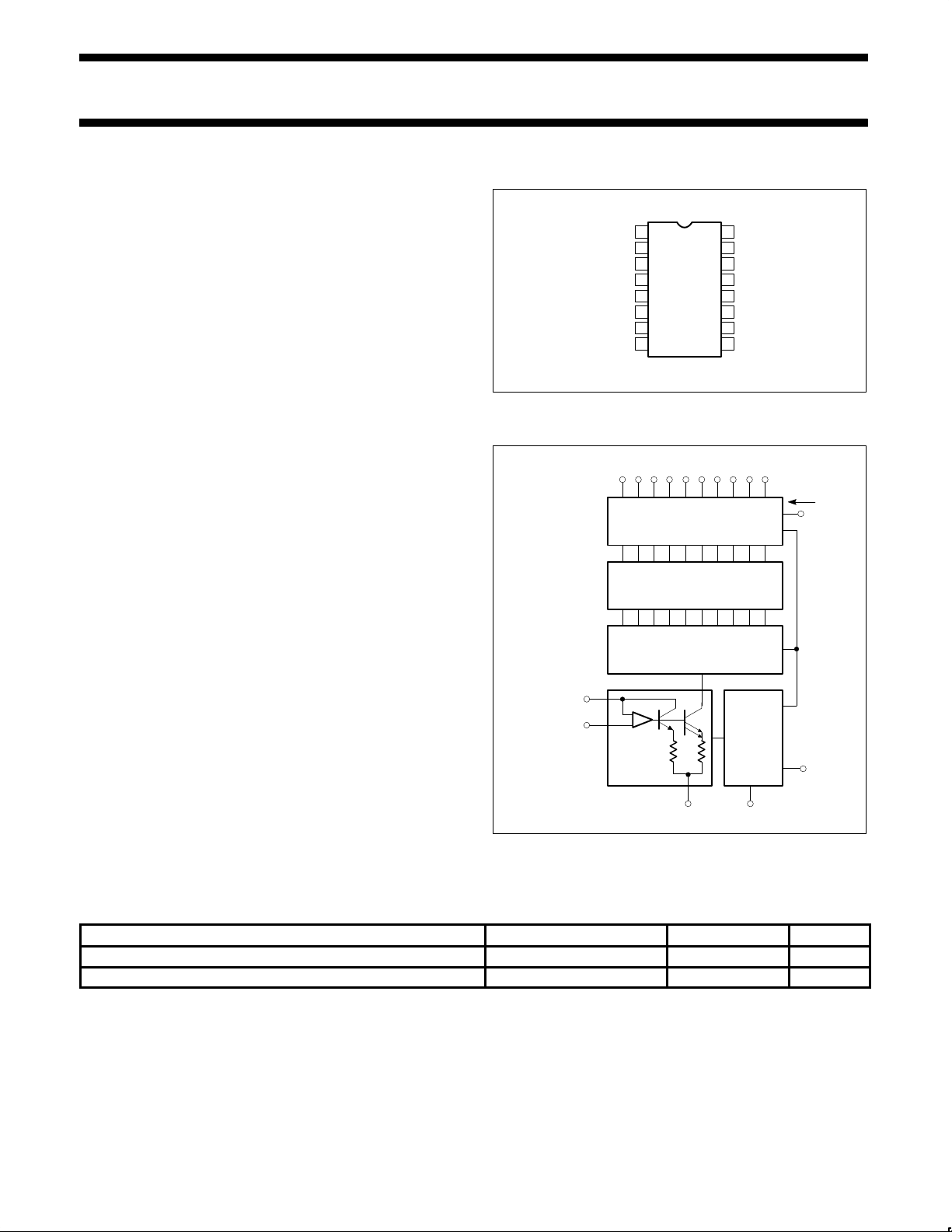
PIN CONFIGURATION
1
2
3
4
5
6
7
8
9
10
11
12
13
14
16
15
F Package
TOP VIEW
V
EE
GND
OUTPUT
D
1
(MSB)
D
2
D
3
D
4
D
5
V
REF
+
D
10
(LSB)
D
9
D
8
D
7
D
6
V
REF
–
V
CC
BLOCK DIAGRAM
MSB LSB
4 5 6 7 8 9 10 11 12 13
3
CURRENT SWITCHES
LADDER TERMINATORS
R-2R LADDER
BIAS
CIRCUITRY
REFERENCE
CURRENT
AMPLIFIER
GND
1 2
14
16
15
D
1D2D3D4D5D6D7D8D9
D
10
V
REF(+)
V
REF(–)
V
CC
I
O
V
EE
ORDERING INFORMATION
DESCRIPTION TEMPERATURE RANGE ORDER CODE DWG #
16-Pin Ceramic Dual In-Line Package (CERDIP) 0 to +70°C NE5410F 0582B
16-Pin Ceramic Dual In-Line Package (CERDIP) -55 to +125°C SE5410F 0582B
Page 2
Philips Semiconductors Linear Products Product specification
NE/SE541010-Bit high-speed multiplying D/A converter
August 31, 1994
768
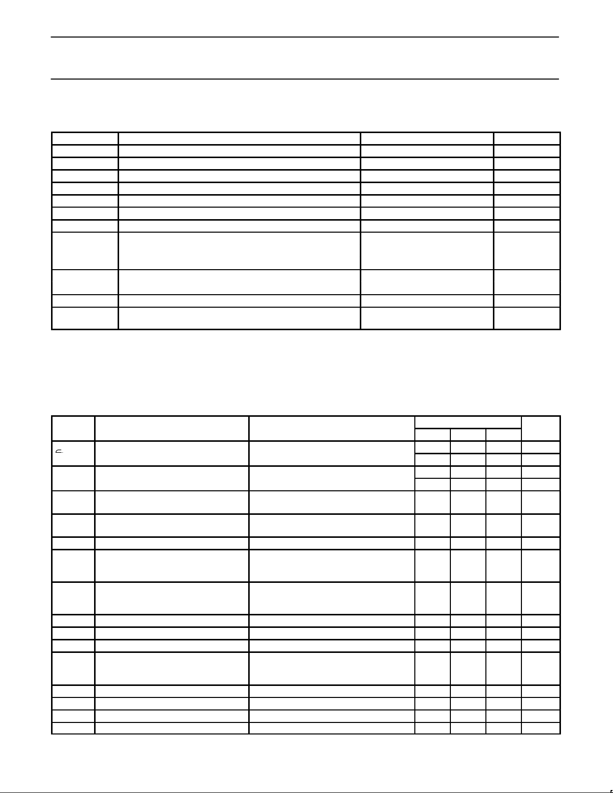
ABSOLUTE MAXIMUM RATINGS
TA=+25°C, unless otherwise specified.
SYMBOL
PARAMETER RATING UNIT
V
CC
Power supply +7.0 V
DC
V
EE
-18 V
DC
V
I
Digital input voltage +15 V
DC
V
O
Applied output voltage +4, -5.0 V
DC
I
REF(16)
Reference current 2.5 mA
V
REF
Reference amplifier inputs VCC, V
EE
V
DC
V
REF(D)
Reference amplifier differential inputs 0.7 V
DC
T
A
Operating temperature range
SE5410 -55 to +125 °C
NE5410 0 to +70 °C
T
J
Junction temperature
Ceramic package +150 °C
T
STG
Storage temperature -65 to +150 °C
P
D
Maximum power dissipation
T
A
=25°C (still-air)
1
1190 mW
NOTES:
1. Derate above 25°C at the following rate:
F package at 9.5mW/°C
DC ELECTRICAL CHARACTERISTICS (Continued)
VCC=+5.0VDC, VEE=-15VDC, I
REF
=2.0mA, all digital inputs at high logic level. SE5410: TA=-55°C to +125°C, NE5410 Series: TA=0°C to +70°C,
unless otherwise noted.
LIMITS
SYMBOL
PARAMETER
TEST CONDITIONS
Min Typ Max
UNIT
Relative accuracy Over Temperature ±0.025 ±0.05 %
∈
R
(Error relative to full scale IO) ±1/4 ±1/2 LSB
Differential non-linearity Over temperature ±0.025 ±0.05 %
±1/4 ±1/2 LSB
t
S
Settling time to within ±1/2 LSB
(all bits low to high)
TA = 25°C 250 ns
t
PLH
t
PHL
Propagation delay time TA = 25°C
35
20
ns
TCI
O
Output full-scale current drift 20 40 ppm/°C
V
IH
Digital input logic levels (all bits)
High level, Logic “1”
Low level, Logic “0”
2.0
0.8
V
DC
I
IH
I
IL
Digital input current (all bits)
High level, V
IH
= 5.5V
Low level, V
IL
= 0.8V
20
–20
µA
I
REF(15)
Reference input bias current (Pin 15) –1.0 –5.0 µA
I
OH
Output current (all bits high) V
REF
= 2.000V, R16 = 1000Ω 3.937 3.996 4.054 mA
I
OL
Output currents (all bits low) TA = 25°C 0 0.4 µA
V
O
Output voltage compliance
TA = 25°C
∈
R
< 0.050%
relative to full-scale
–2.5
+2.5
V
DC
SR I
REF
Reference amplifier slew rate 20 mA/µs
ST I
REF
Reference amplifier settling time 0 to 4.0mA, ±0.1% 2.0 µs
PSRR(–) Output current power supply sensitivity 0.003 0.01 %/%
C
O
Output capacitance VO = 0 25 pF
Page 3

Philips Semiconductors Linear Products Product specification
NE/SE541010-Bit high-speed multiplying D/A converter
August 31, 1994
769
DC ELECTRICAL CHARACTERISTICS
VCC=+5.0VDC, VEE=-15VDC, I
REF
=2.0mA, all digital inputs at high logic level. SE5410: TA=-55°C to +125°C, NE5410 Series: TA=0°C to +70°C,
unless otherwise noted.
LIMITS
SYMBOL
PARAMETER
TEST CONDITIONS
Min Typ Max
UNIT
C
I
Digital input capacitance (all bits high) 4.0 pF
I
CC
I
EE
Power supply current (all bits low)
+2
–12
+4
–18
mA
V
CC
V
EE
Power supply voltage range
TA = 25°C
V
O
= 0
+4.75
–14.25
+5.0
–15
+5.25
–15.75
V
DC
Power consumption 190 300 mW
COMPLIANCE VOLTAGE (VOLT)
Figure 1. Output Current vs Output Compliance Voltage
OUTPUT CURRENT (mA)
4.0
3.0
2.0
1.0
0
–1.0
–5 –3 –1 0 1 3 5
+VCC = +5V
–VEE = –15V
I
REF
= 2mA
TA = 25°C
OUTPUT COMPLIANCE VOLTAGE (VOLTS)
Figure 2. Maximum Output Compliance Voltage
vs Temperature
4.0
3.0
2.0
1.0
0
–1.0
–2.0
–3.0
–4.0
–75 –50 –25 0 25 50 75 100 125
T
A
(°C)
+VCC = +5V
–VEE = –15V
I
REF
= 2mA
CIRCUIT DESCRIPTION
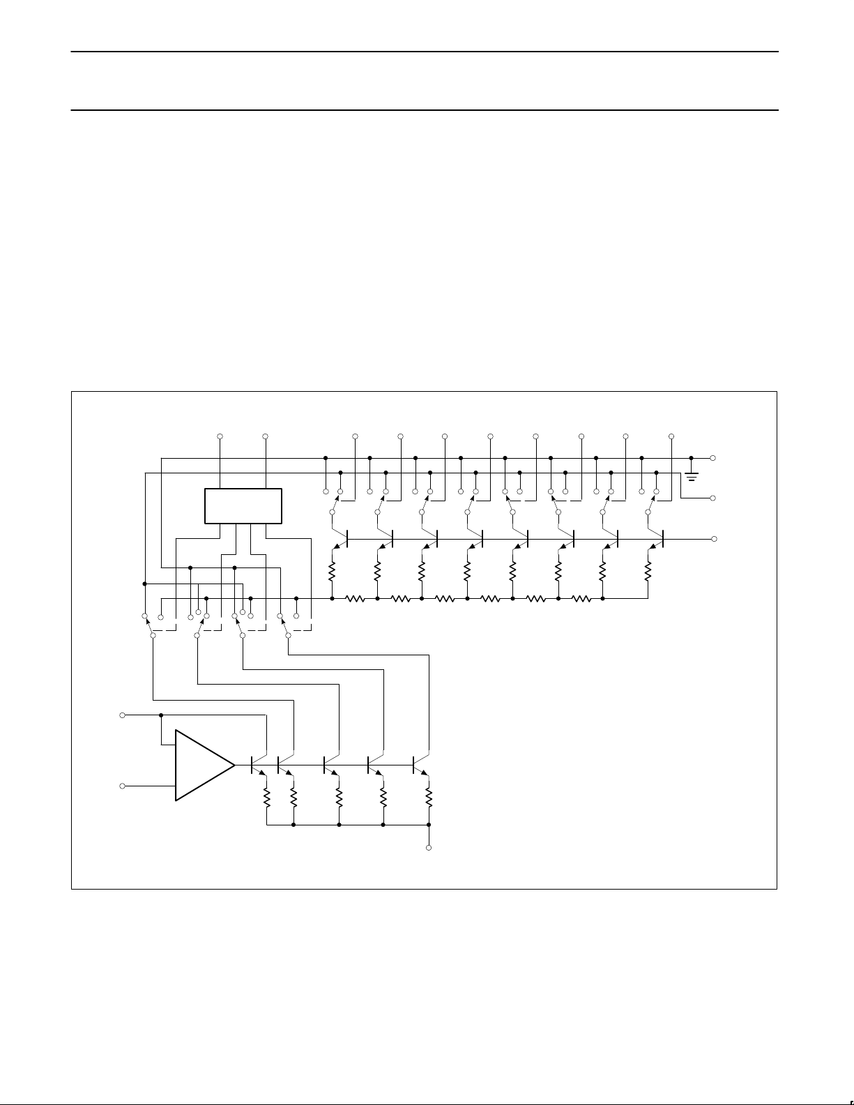
The NE5410 consists of four segment current sources which
generate the 2 Most Significant Bits (MSBs), and an R/2R DAC
implemented with ion-implanted resistors for scaling the remaining 8
Least Significant Bits (LSBs) (see Figure 5). This approach provides
complete 10-bit accuracy without trimming.
The individual bit currents are switched ON or OFF by
fully-differential current switches. The switches use current steering
for speed.
Figure 3. Power Supply Currents vs Temperature
POWER SUPPLY CURRENT (mA)
13
12
11
10
4
3
2
1
0
–75 –50 –25 0 25 50 75 100 125
T
A
(°C)
+VCC = +5V
–VEE = –15V
I
REF
= 2mA
I
EE
+I
CC
II
CC EE
Figure 4. Reference Amplifier Frequency Response
An on-chip high slew reference current amplifier drives the R/2R
ladder and segment decoder. The currents are scaled in such a way
that, with all bits on, the maximum output current is two times
1023/1024 of the reference amplifier current, or nominally 3.996mA
for a 2.000mA reference input current. The reference amplifier
allows the user to provide a voltage input: out-board resistor R16
(see Figure 6) converts this voltage to a usable current. A current
mirror doubles this reference current and feeds it to the segment
decoder and resistor ladder. Thus, for a reference voltage of 2.0V
and a 1kΩ resistor tied to Pin 16, the full-scale current is
Page 4
Philips Semiconductors Linear Products Product specification
NE/SE541010-Bit high-speed multiplying D/A converter
August 31, 1994
770
approximately 4.0mA. This relationship will remain regardless of the
reference voltage polarity.
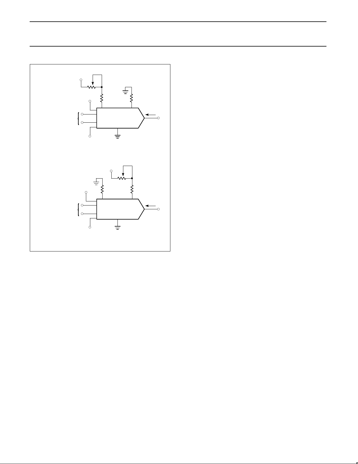
Connections for a positive reference voltage are shown in Figure 6a.
For negative reference voltage inputs, or for bipolar reference
voltage inputs in the multiplying mode, R15 can be tied to a negative
voltage corresponding to the minimum input level. For a negative
reference input, R16 should be grounded (Figure 6b). In addition,
the negative voltage reference must be at least 3V above the V
EE
supply voltage for best operation. Bipolar input signals may be
handled by connecting R16 to a positive voltage equal to the peak
positive input level at Pin 15.
When a DC reference voltage is used, capacitive bypass to ground
is recommended. The 5V logic supply is not recommended as a
reference voltage. If a well regulated 5.0V supply, which drives logic,
is to be used as the reference, R16 should be decoupled by
connecting it to the +5.0V logic supply through another resistor and
bypassing the junction of the two resistors with a 0.1µF capacitor to
ground.
The reference amplifier is internally-compensated with a 10pF
feed-forward capacitor, which gives it its high slew rate and fast
settling time. Proper phase margin is maintained with all possible
values of R16 and reference voltages which supply 2.0mA reference
current into Pin 16. The reference current can also be supplied by a
high impedance current source of 2.0mA. As R16 increases, the
bandwidth of the amplifier decreases slightly and settling time
increases. For a current source with a dynamic output impedance of
1.0MΩ, the bandwidth of the reference amplifier is approximately
half what it is in the case of R16=1.0kΩ, and settling time is ±10µs.
The reference amplifier phase margin decreases as the current
source value decreases in the case of a current source reference,
so that the minimum reference current supplied from a current
source is 0.5mA for stability.
CODE SELECTED 0111110011
Figure 5. NE5410 Equivalent Circuit
R
MSB
LSB
(4)
(5) (6) (7) (8) (9) (10) (11) (12)
(13)
GND
(2)
(3)
(INTERNAL)
2R
SEGMENT
DECODER
(15)
(16)
+
–
R
2R
R
2R
R
2R
R
2R
R
2R 2R 2R
2R
1
R
1
R
1
R
1
R
1
VEE (1)
V
REF
+
–
V
BIAS
I
OUT
D
1
D
2
D
3
D
4
D
5
D
6
D
7
D
8
D
9
D
10
Page 5
Philips Semiconductors Linear Products Product specification
NE/SE541010-Bit high-speed multiplying D/A converter
August 31, 1994
771
Figure 6. Basic Connections
a. Positive Reference Voltage
b. Negative Reference Voltage
NOTES:
R
16
+ RT = R15 = R
REF
RT < <R
16
IO F.S. = 2 IR = V
REF/RREF
NOTES:
R
15
+ RT = R
16
RT < <R
15
IV
REF
≥ R
VEE
+ 3V
14
16
15
3
2
1
5410
D
1
THROUGH D
10
VR (+)
V
CC
V
EE
R
T
R
15
R
16
I
O
15
13
2
1
5410
D1 THROUGH D
10
VR (–)
V
CC
V
EE
R
T
R
15
R
16
I
O
OUTPUT VOLTAGE COMPLIANCE
The output voltage compliance ranges from -2.5 to +2.5V. As shown
in Figure 2, this compliance range is nearly constant over
temperature. At the temperature extremes, however, the compliance
voltage may be reduced if V
EE
>-15V.
ACCURACY
Absolute accuracy is a measure of each output current level with
respect to its intended value. It is dependent upon relative accuracy
and full-scale current drift. Relative accuracy, or linearity, is the
measure of each output current with respect to its intended fraction
of the full-scale current. The relative accuracy of the NE5410 is fairly
constant over temperature due to the excellent temperature tracking,
of the implanted resistors. The full-scale current from the reference
amplifier may drift with temperature causing a change in the
absolute accuracy. However, the NE5410 has a low full-scale
current drift with temperature.
The SE5410 and the NE5410 are accurate to within ± LSB at 25°C
with a reference current of 2.0mA on Pin 16.
MONOTONICITY
The NE5410 and SE5410 are guaranteed monotonic over
temperature. This means that for every increase in the input digital
code, the output current either remains the same or increases but
never decreases. In the multiplying mode, where reference input
current will vary, monotonicity can be assured if the reference input
current remains above 0.5mA.
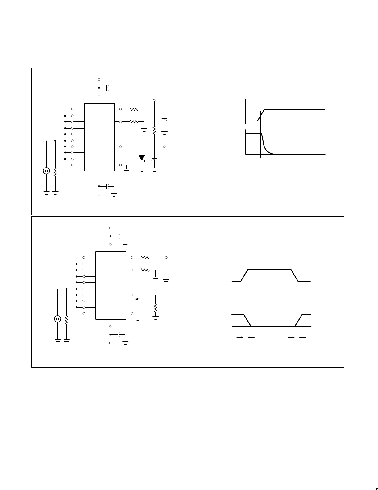
SETTLING TIME
The worst-case switching condition occurs when all bits are
switched “on,” which corresponds to a LOW-to-HIGH transition for
all bits. This time is typically 250ns for the output to settle to within ±
1/2LSB for 10-bit accuracy, and 200ns for 8-bit accuracy. The
turn-off time is typically 120ns. These times apply when the output
swing is limited to a small (<0.7V) swing and the external output
capacitance is under 25pF.
The major carry (MSB off-to-on, all others on-to-off) settles in
approximately the same time as when all bits are switched off-to-on.
If a load resistor of 625Ω is connected to ground, allowing the output
to swing to -2.5V, the settling time increases to 1.5µs.
Extra care must be taken in board layout as this is usually the
dominant factor in satisfactory test results when measuring settling
time. Short leads, 100µF supply bypassing, and minimum scope
lead length are all necessary.
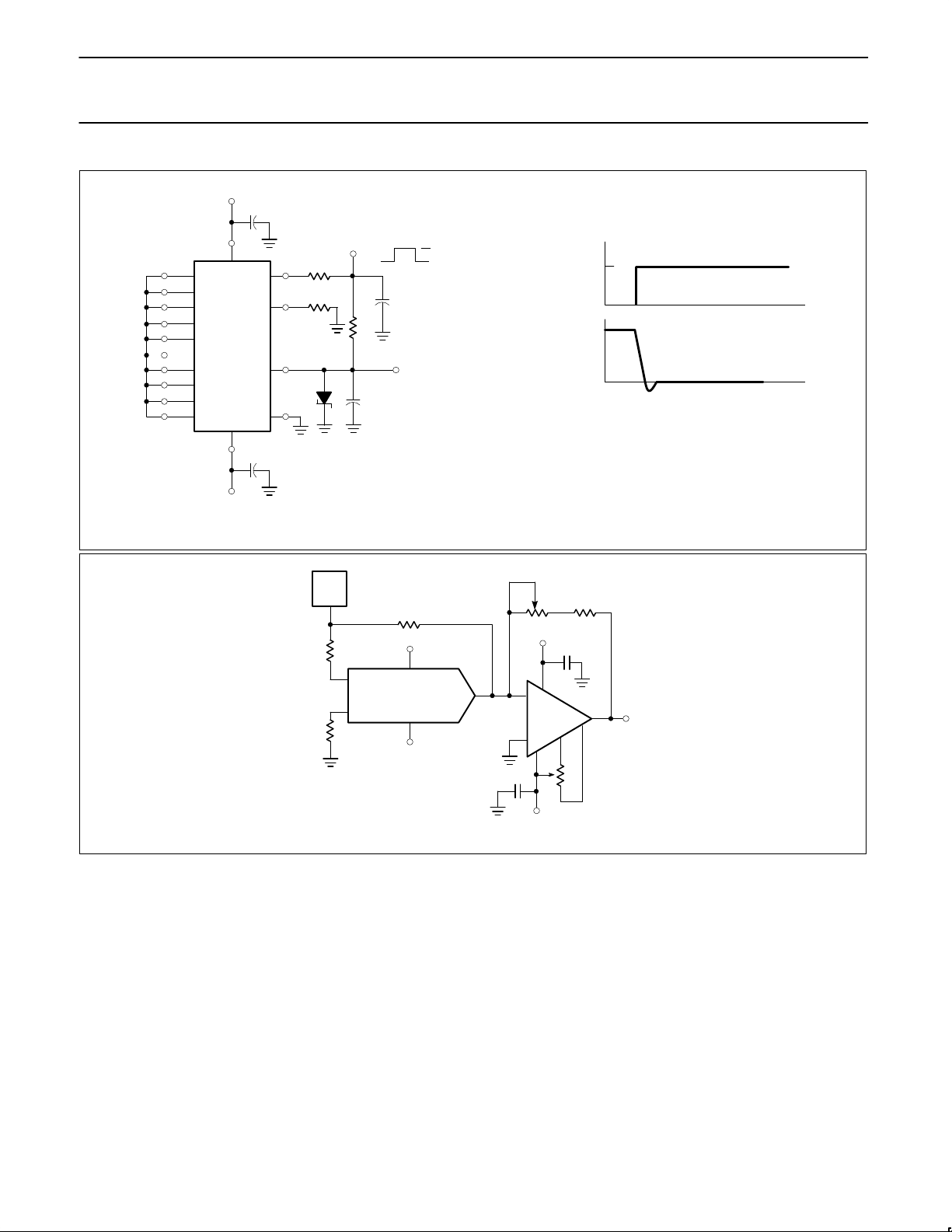
A typical test setup for measuring settling time is shown in Figure 7.
The same setup for the most part can be used to measure the slew
rate of the reference amplifier (Figure 9) by tying all data bits high,
pulsing the voltage reference input between 0 and 2V , and using a
500Ω load resistor R
L
.
Page 6
Philips Semiconductors Linear Products Product specification
NE/SE541010-Bit high-speed multiplying D/A converter
August 31, 1994
772
Figure 7. Settling Time
4
5
6
7
8
9
10
11
12
13
14
1
16
15
3
2
1k
1k
50
+2VDC
500
V
CC
V
EE
R
L
V
O
CO ≤ 25pF
NE5410
V
I
0.1µF
0.1µF
0.1µF
2.4V
0.4V
0.5V
0
t
S
— 250ns TYPICAL
TO ± 1/2 LSB
RISE AND FALL TIMES ≤ 10ns
V
O
V
I
Figure 8. Propagation Delay Time
4
5
6
7
8
9
10
11
12
13
14
1
16
15
3
2
1k
1k
50
+2VDC
20
V
CC
V
EE
R
L
V
O
NE5410
V
I
0.1µF
0.1µF
0.1µF
2.4V
0.4V
–80mV
0V
t
PLH
TO ± 1/2 LSB
RISE AND FALL TIMES ≤ 10ns
V
O
V
I
t
PHL
FOR PROPAGATION
DELAY TIME
Page 7
Philips Semiconductors Linear Products Product specification
NE/SE541010-Bit high-speed multiplying D/A converter
August 31, 1994
773
TO ±0.1%
Figure 9. Reference Amplifier Settling Time and Slew Rate
4
5
6
7
8
9
10
11
12
13
14
1
16
15
3
2
1k
1k
500
V
CC
V
EE
R
L
V
O
≤ 25pF
NE5410
0.1µF
0.1µF
0.1µF
V
REF
(+)
2V
0
2.0V
0
0
0.5V
V
O
V
REF
(+)
SLEW RATE
tS = 2µs TYPICAL
NOTE:
Use RL = 20Ω to GND for slew rate measurement.
Figure 10. Bipolar Voltage Output Circuits (-10V to +10V)
2.5k
5410
R
T
0.1µF
V
EE
V
CC
16
2.5k
R
REF
15
0
ADJ
–15V
10k
V
OUT
+15V
F.S. ADJ
R
F
5V
REF
2.5k
0.1µF
1/2 NE5535
Page 8
Philips Semiconductors Linear Products Product specification
NE/SE541010-Bit high-speed multiplying D/A converter
August 31, 1994
774
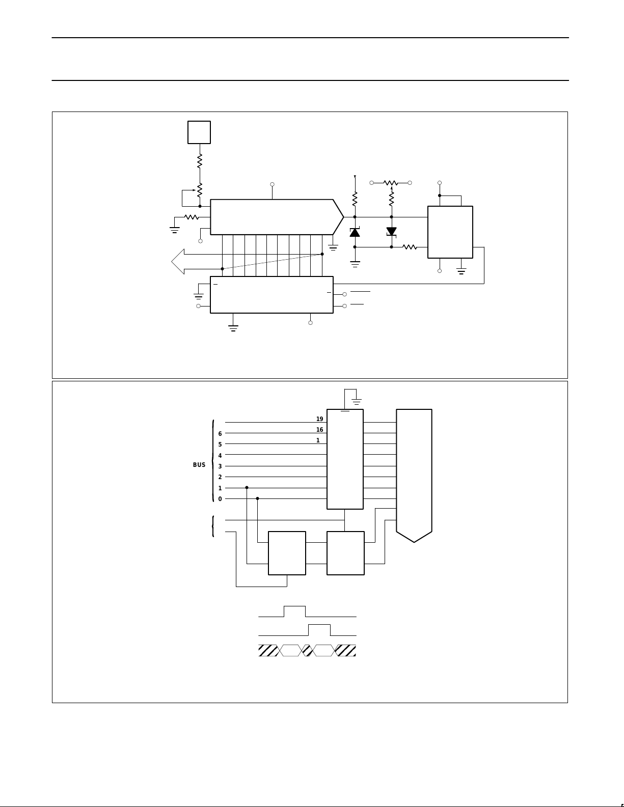
Figure 11. Successive Approximation A/D Converter
NOTES:
10-bit conversion time = 3.3µs with 3MHz clock.
This converter uses a 2504 12-bit successive approximation register in the short cycle operating mode where the end of conversion signal is taken from the first unused bit of the
SAR (Q
10
).
2.4k
F.S.
ADJ
16
2.5k
15
–15VDC
CLOCK CP
2504 SAR
NE5410
+5VDC
2.5k
3
D
+5VDC
ANALOG
INPUT
(0-10V)
–V
20k
ZERO
ADJ
500k
2.5k
3
4
+V
+5VDC
1 14
IN B OUT A
6
10
–10VDC
200Ω
D
OUT
V1+V
2+
Q
9
Q
0
Q
10
E
S
NE529
START
EOC
5V
REF
IN A
Figure 12. 8-Bit µP Bus Interface
NOTES:
With this double latch technique, valid data will be latched to the DAC until updated with the E
2
pulse. Timing will depend on the processor used.
NE5410
7
6
5
4
3
2
1
0
BUS
19
16
15
12
9
6
5
2
11
13
1
7
2
6
1/2 LS375
4
CONTROL
SIGNALS
TIMING SEQUENCE
DATA
LS373
1
FROM µP
µP
E
2
E
1
D
0
D
1
Q
0
Q
1
E
0,1
E
2,3
Q
2
Q
3
E
1
E
2
DB
0,1
DB
2-9
OE
1/2LS375
Page 9
Philips Semiconductors Linear Products Product specification
NE/SE541010-Bit high-speed multiplying D/A converter
August 31, 1994
775
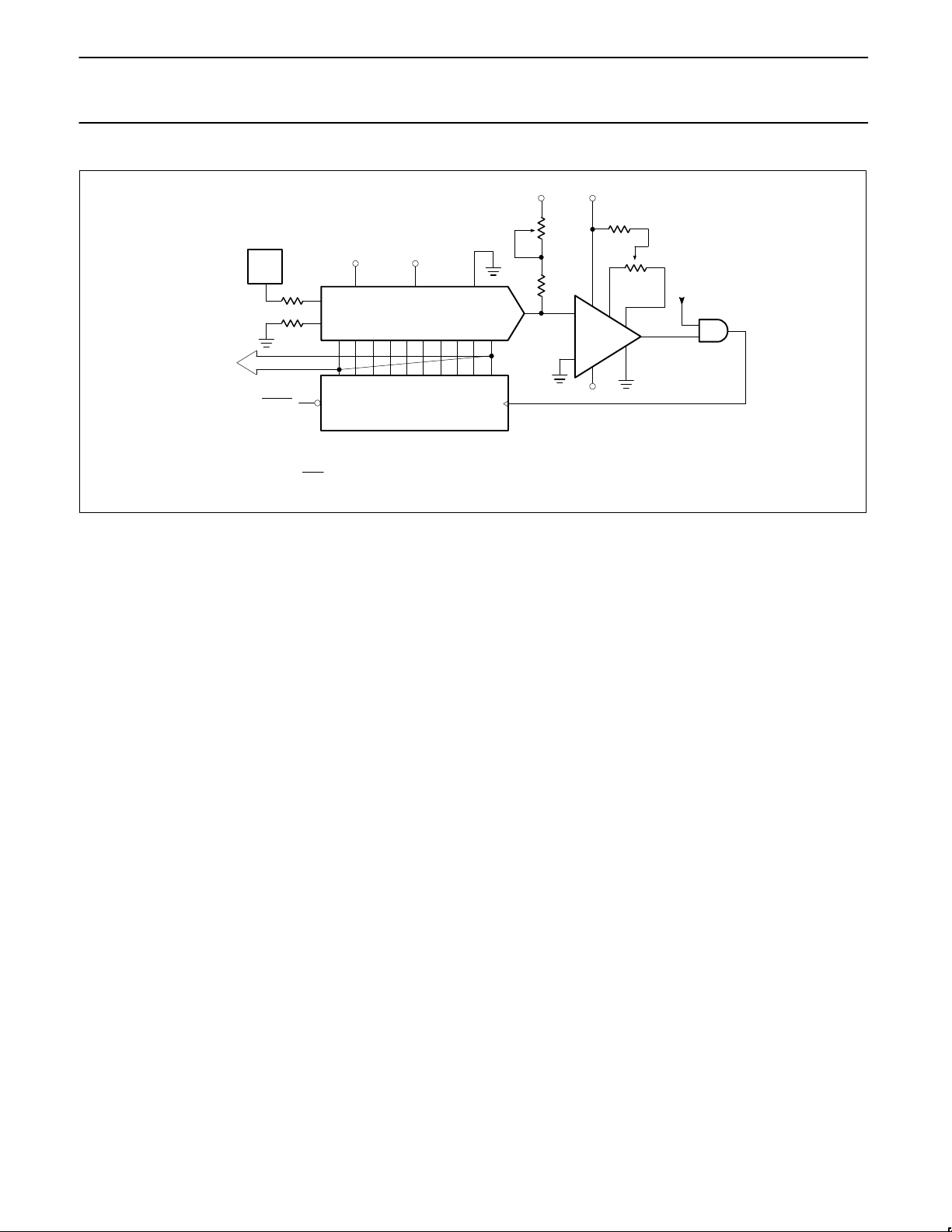
Figure 13. Staircase A/D
NOTE:
VINFULL SCALE 4mA (R1 RT)
1023
1024
15
13
RST
NE5410
3
TTL
–15
MSB
D
OUT
Q
0
Q
9
CP
START
5V
REF
LSB 12 11 10 9 8 7 6 5 4
CLOCK
ZERO
ADJ
3k
3k
+5V
14 1
16
2.5k
2.5k
COMP
+
–
R
T
R
I
V
IN
10-BIT COUNTER
2
V
CC
V
EE
 Loading...