

Page 1
Philips Semiconductors Linear Products Product specification
NE/SE521High-speed dual-differential comparator/sense amp
305
August 31, 1994 853-0900 13721
FEATURES
•12ns maximum guaranteed propagation delay
•20µA maximum input bias current
•TTL compatible strobes and outputs
•Large common-mode input voltage range
•Operates from standard supply voltages
•Military qualifications pending
APPLICATIONS
•MOS memory sense amp
•A-to-D conversion
•High-speed line receiver
PIN CONFIGURATION
1
2
3
4
5
6
7 8
14
13
12
11
10
9
D, F, N Packages
INPUT 1A
INPUT 1B
NC
OUTPUT 1Y
STROBE 1G
STROBE S
GND
V+
V–
INPUT 2A
INPUT 2B
NC
OUTPUT 2Y
STROBE 2G
TOP VIEW
ORDERING INFORMATION
DESCRIPTION TEMPERATURE RANGE ORDER CODE DWG #
14-Pin Plastic Dual In-Line Package (DIP) 0 to +70°C NE521N 0405B
14-Pin SO Package 0 to +70°C NE521D 0175D
14-Pin Ceramic Dual In-Line Package (CERDIP) 0 to +70°C NE521F 0581B
14-Pin Ceramic Dual In-Line Package (CERDIP) -55°C to +125°C SE521F 0581B
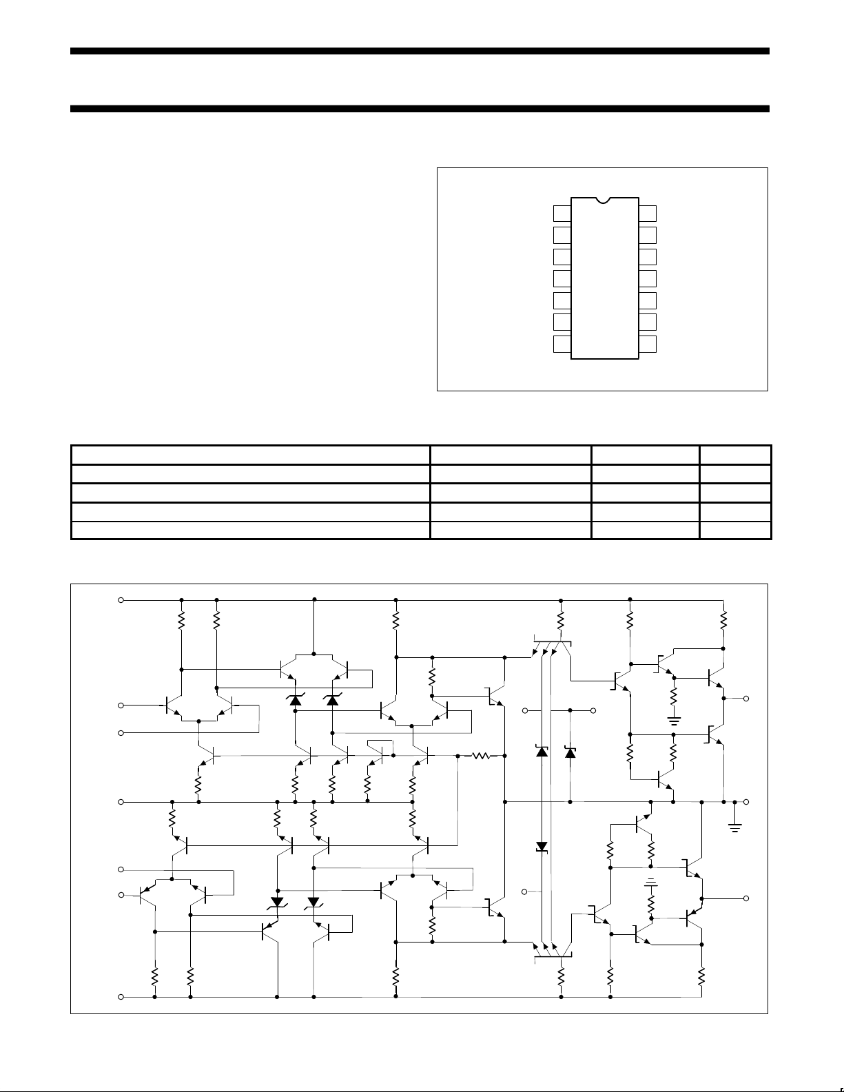
EQUIVALENT SCHEMATIC
Q11
V+
14
2
–
+
1
V–
13
R2 R1
Q2 Q1
Q4
Q3
D7
Q9
R4
Q10 Q8
R5 R3
D6
R17
Q6
R16
Q5
Q13
R15 R6
R9
Q19
Q7
R14
5
D2
Q25
R20
6
R21
Q26
Q30
R24
R23
Q27
Q29
Q28
R25
7
12
+
–
11
V+
R8
Q16
Q15 Q14
R12 R11
Q18
R10
Q17
D4
Q20
Q21
R7
D5
Q22 Q23
R18
R19
D3
8
Q24
Q31
R26
Q32
R27
R28
Q36
R29
R30
Q32
Q35
9
Q34
R34
R22
4
Page 2
Philips Semiconductors Linear Products Product specification
NE/SE521High-speed dual-differential comparator/sense amp
August 31, 1994
306
LOGIC FUNCTIONS
V
ID
A+, B
–
STROBE S STROBE G OUTPUT (Y)
VID≤-V
OS
H H L
-VOS<VID<V
OS
H H Undefined
VID≥V
OS
H H H
X L X H
X X L H
ABSOLUTE MAXIMUM RATINGS
SYMBOL PARAMETER RATING UNIT
Supply voltage
V+ Positive +7 V
V- Negative -7 V
V
IDR
Differential input voltage ±6 V
V
IN
Input voltage
Common mode ±5 V
Strobe/gate +5.25 V
P
D
Maximum power dissipation
1
TA= 25°C (still-air)
F package 1190 mW
N package 1420 mW
D package 1040 mW
T
A
Operating temperature range
NE521 0 to 70 °C
SE521 -55 to +125 °C
T
STG
Storage temperature range -65 to +150 °C
T
SOLD
Lead soldering temperature (10 sec. max) +300 °C
NOTES:
1. Derate above 25°C at the following rates:
F package at 9.5mW/°C
N package at 11.4mW/°C
D package at 8.3mW/°C
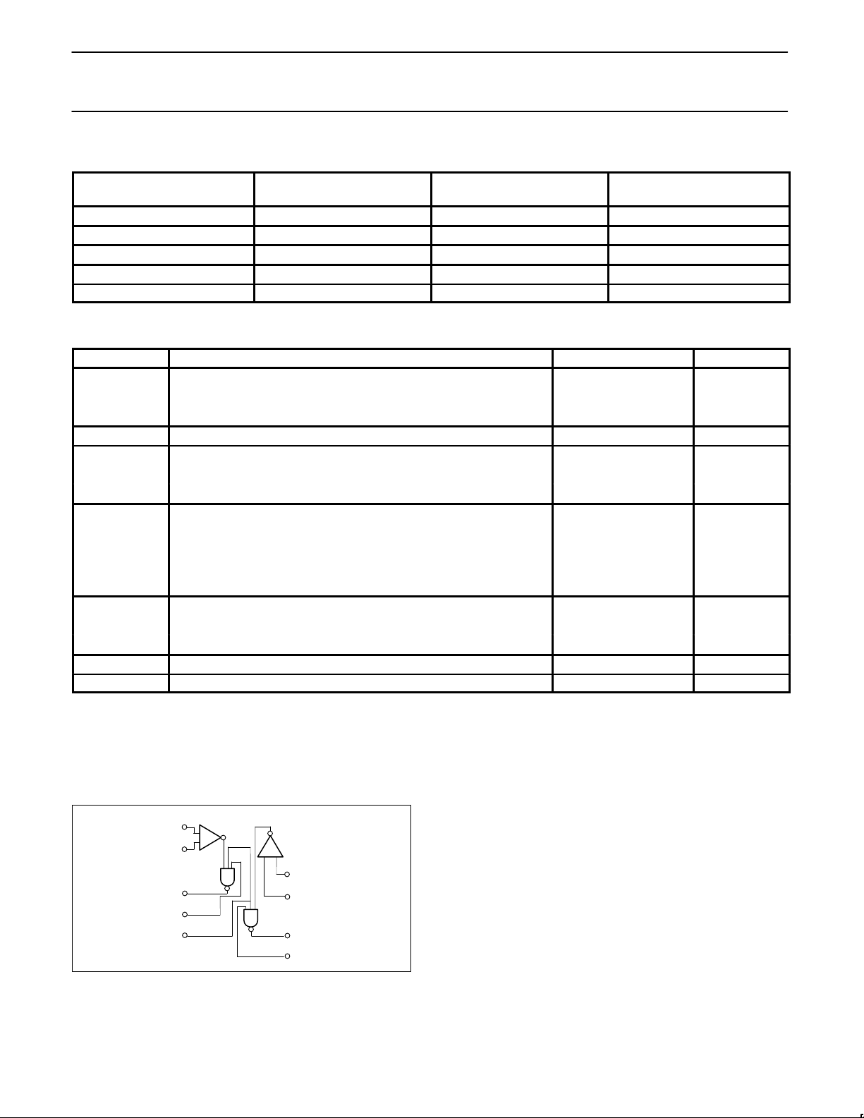
BLOCK DIAGRAM
(12)
INPUT 2A
(11)
INPUT 2B
(9)
OUTPUT 3Y
(8)
STROBE 2G
(1)
(2)
(4)
(5)
INPUT 1A
INPUT 1B
OUTPUT 1Y
STROBE 1G
(60
STROBE S
Page 3
Philips Semiconductors Linear Products Product specification
NE/SE521High-speed dual-differential comparator/sense amp
August 31, 1994
307
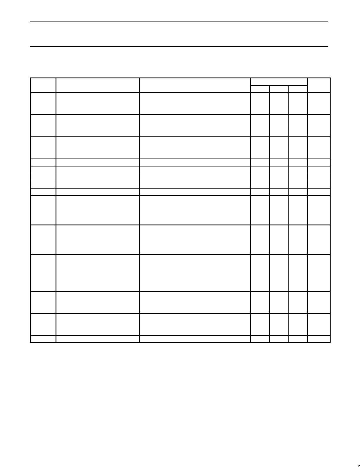
DC ELECTRICAL CHARACTERISTICS (SE521)
V+=+5V, V-=-5V, TA=-55°C to +125°C, unless otherwise specified.
LIMITS
SYMBOL
PARAMETER
TEST CONDITIONS
Min Typ Max
UNIT
V
OS
Input offset voltage V+=+4.5V, V-=-4.5V
At 25°C 6 7.5 mV
Over temperature range 15
I
BIAS
Input bias current V+=+5.5V, V-=-5.5V
At 25°C 7.5 20 µA
Over temperature range 40
I
OS
Input offset current V+=+5.5V, V-=-5.5V
At 25°C 1.0 5 µA
Over temperature range 12
V
CM
Common-mode voltage range V+=+4.5V, V-=-4.5V –3 +3 V
V
IL
Low level input voltage
At 25°C 0.8 V
Over temperature 0.7
V
IH
High level input voltage 2.0 V
Input current V+=+5.5V, V-=-5.5V
I
IH
High VIH=2.7V
1G or 2G strobe 50 µA
Common strobe S 100 µA
Input Current
I
IL
Low VIL=0.5V
1G or 2G strobe -2.0 mA
Common strobe S -4.0 mA
Output voltage V
I(S)
=2.0V
V
OH
High V+=+4.5V, V-=-4.5V, I
LOAD
=-1mA 2.5 3.4
V
V
OL
Low V+=+4.5V, V-=-4.5V, I
LOAD
=10mA 0.5
TA=25°C, I
LOAD
=20mA 0.5
Supply voltage
V+ Positive 4.5 5.0 5.5 V
V- Negative -4.5 -5.0 -5.5
Supply current V+=5.5V, V-=-5.5V, TA=25°C
I
CC+
Positive 27 35 mA
I
CC-
Negative -15 -28
I
SC
Short-circuit output current -35 -115 mA
Page 4
Philips Semiconductors Linear Products Product specification
NE/SE521High-speed dual-differential comparator/sense amp
August 31, 1994
308
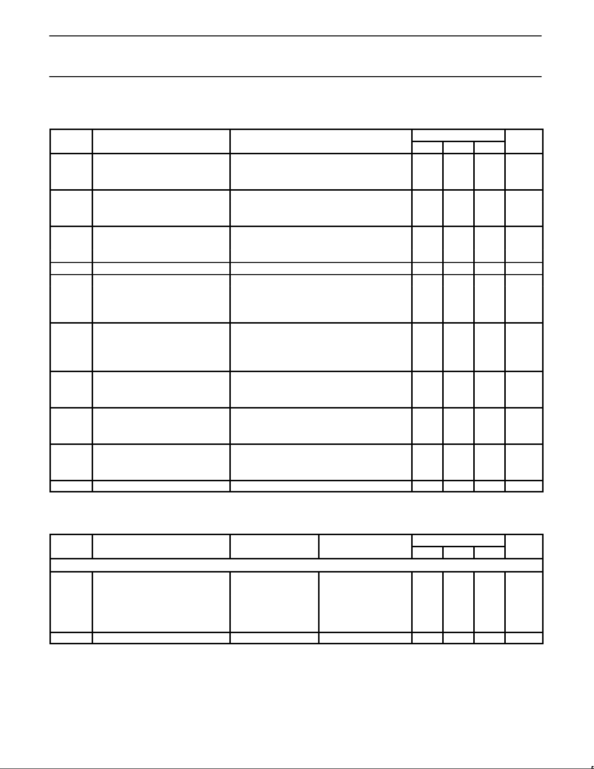
DC ELECTRICAL CHARACTERISTICS(NE521)
V+=+5V, V-=-5V, TA=0 to 70°C, unless otherwise specified.
LIMITS
SYMBOL
PARAMETER
TEST CONDITIONS
Min Typ Max
UNIT
V
OS
Input offset voltage V+=+4.75V, V-=-4.75V
At 25°C 6 7.5 mV
Over temperature range 10
I
BIAS
Input bias current V+=+5.25V, V-=-5.25V
At 25°C 7.5 20 µA
Over temperature range 40
I
OS
Input offset current V+=+5.25V, V-=-5.25V
At 25°C 1.0 5 µA
Over temperature range 12
V
CM
Common-mode voltage range V+=+4.75V, V-=-4.75V –3 +3 V
Input current V+=+5.25V, V-=-5.25V
I
IH
High VIH=2.7V
1G or 2G strobe 50 µA
Common strobe S 100 µA
Input Current
I
IL
Low VIL=0.5V
1G or 2G strobe -2.0 mA
Common strobe S -4.0 mA
Output voltage V
I(S)
=2.0V
V
OH
High V+=+4.75V, V-=-4.75V, I
LOAD
=-1mA 2.7 3.4 V
V
OL
Low V+=+5.25V, V-=-5.25V, I
LOAD
=20mA 0.5
Supply voltage
V+ Positive 4.75 5.0 5.25 V
V- Negative -4.75 -5.0 -5.25
Supply current V+=5.25V, V-=-5.25V, TA=25°C
I
CC+
Positive 27 35 mA
I
CC-
Negative -15 -28
I
SC
Short-circuit output current -40 -100 mA
AC ELECTRICAL CHARACTERISTICS
TA=25°C, RL=280W CL=15pF V+=5V V-=5V.
LIMITS
SYMBOL
PARAMETER
FROM INPUT
TO OUTPUT
Min Typ Max
UNIT
Large-signal switching speed
Propagation delay
t
PLH(D)
Low to high
1
Amp Output 8 12
t
PHL(D)
High to low
1
Amp Output 6 9 ns
t
PLH(S)
Low to high
2
Strobe Output 4.5 10
t
PHL(S)
High to low
2
Strobe Output 3.0 6
f
MAX
Max. operating frequency 40 55 MHz
NOTES:
1. Response time measured from 0V point of ±100mV
P-P
10MHz square wave to the 1.5V point of the output.
2. Response time measured from 1.5V point of input to 1.5V point of the output.
Page 5
Philips Semiconductors Linear Products Product specification
NE/SE521High-speed dual-differential comparator/sense amp
August 31, 1994
309
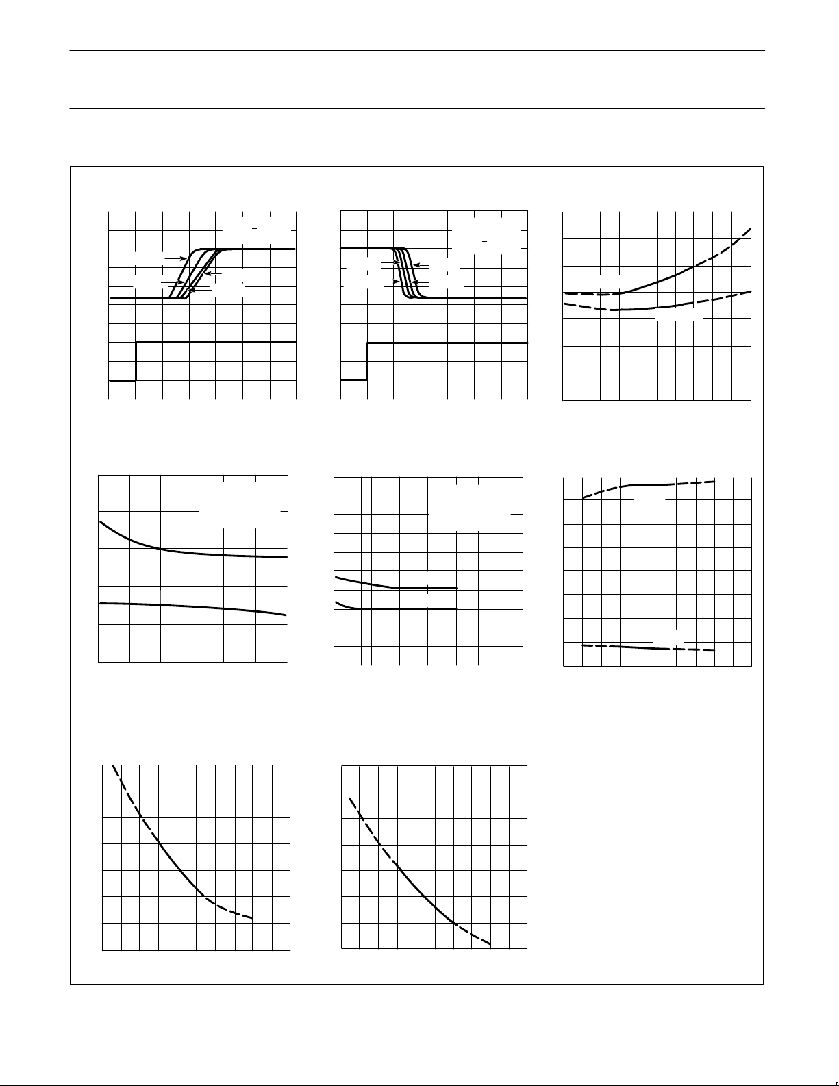
TYPICAL PERFORMANCE CHARACTERISTICS
20mV
5mV
10mV
Response Time for Various
Input Overdrives
Response Time for Various
Input Overdrives
Response Time vs Temperature
Propagation Delay for
Various Input Voltages
Propagation Delay for
Various Input Voltages
Output Voltage vs
Ambient Temperature
Input Bias Current vs
Ambient Temperature
Input Offset Current vs
Ambient Temperature
4
3
2
1
0
100
50
0
0 5 10 15 20 25 30
VS = +5V
T
A
= 25oC
100mV
TIME — nS
INPUT VOLTAGE (mV) OUTPUT VOLTAGE (V)
TA = 25oC
V
S
= +5V
5mV
10mV100mV
50mV
0 5 10 15 20 25 30
TIME — nS
INPUT VOLTAGE (mV) OUTPUT VOLTAGE (V)
4
3
2
1
0
100
50
0
12
10
8
6
4
2
60 20 –20 +60 +100 +140
TPD (LH)
TPD (HL)
AMBIENT TEMPERATURE (
o
C)
TESPONSE TIME (ns)
INPUT VOLTAGE (mVp–p)
PROPAGATION DELAY (ns)
VS = +5V
10MHz SQUARE
WAVE INPUT
T
A
= 25oC
TPD (LH)
TPD (HL)
10 20 30 40 50 60 70
12
10
8
6
20
18
16
14
12
10
8
6
4
2
100
1000
INPUT VOLTAGE (m Vp–p)
PROPAGATION DELAY (ns)
VS = +5V
10MHz SQUARE
WAVE INPUT
T
A
= 25oC
TPD (LH)
TPD (HL)
4.0
3.0
2.0
1.0
–75
–25
+25
+75 +125
V
OL
V
OH
AMBIENT TEMPERATURE (
o
C)
OUTPUT VOLTAGE (V)
–75 –25 +25 +75 +125
AMBIENT TEMPERATURE (oC)
12
11
10
9
8
7
6
INPT BIAS CURRENT ( A)
µ
1.1
1.0
0.9
0.8
0.7
0.6
0.5
–75 –25 +25 +75 +125
AMBIENT TEMPERATURES (
o
C)
INPUT OFSET CURRENT ( A)
µ
 Loading...