

Page 1
Philips Semiconductors Linear Products Product specification
NE/SE5018/50198-Bit µp-compatible D/A converter
751
August 31, 1994 853-0845 13721
DESCRIPTION
The NE/SE5018/19 is a complete 8-bit digital-to-analog converter
subsystem on one monolithic chip. The data inputs have input
latches which are controlled by a latch enable pin. The data and
latch enable inputs are ultra-low loading for easy interfacing with all
logic systems. The latches appear transparent when the LE
input is
in the low state. When LE
goes high, the input data present at the
moment of transition is latched and retained until LE
again goes low.
This feature allows easy compatibility with most microprocessors.
The chip also comprises a stable voltage reference (5V nominal)
and high slew rate buffer amplifier. The voltage reference may be
externally trimmed with a potentiometer for easy adjustment of
full-scale while maintaining a low temperature coefficient.
The output of the buffer amplifier may be offset so as to provide
bipolar as well as unipolar operation.
FEATURES
•8-bit resolution
•Input latches
•Low-loading data inputs
•On-chip voltage reference
•Output buffer amplifier
•Accurate to ± LSB (0.19%)
•Monotonic to 8 bits
•Amplifier and reference both short-circuit protected
•Compatible with 8085, 6800 and many other µPs
APPLICATIONS
•Precision 8-bit D/A converters
•A/D converters
•Programmable power supplies
•Test equipment
•Measuring instruments
•Analog-digital multiplication
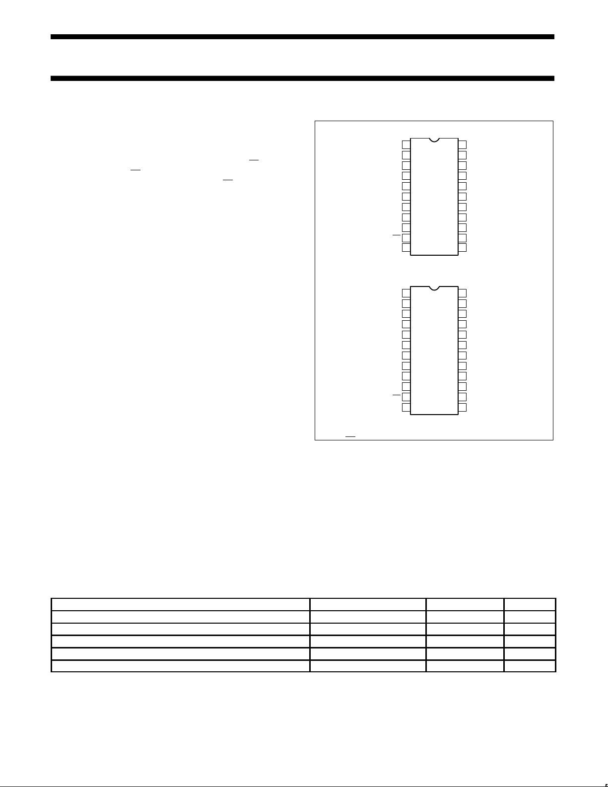
PIN CONFIGURATIONS
1
2
3
4
5
6
7
8
9
10
11
12
13
14
24
23
22
21
20
19
18
17
16
15
1
2
3
4
5
6
7
8
9
10
13
14
15
16
22
21
20
19
18
17
F, N Packages
D Package
1
NOTE:
1. SOL and
non-standard pinout
11
12
DIGITAL GND
DB0(LSB)
DB1
DB2
DB3
DB4
DB5
DB6
DB7(MSB)
NC
ANALOG GND
AMP COMP
SUM MODE
DAC COMP
BIPOLAR
OFFSET R
LE
V
CC+
V
OUT
V
CC–
V
REF
IN
V
REF
OUT
V
REF
ADJ
DIGITAL GND
DB0(LSB)
DB1
DB2
DB3
DB4
DB5
DB6
DB7(MSB)
NC
ANALOG GND
AMP COMP
SUM MODE
DAC COMP
BIPOLAR
OFFSET
LE
V
CC+
V
OUT
V
CC–
V
REF
IN
V
REF
OUT
V
REF
ADJ
NC
NC
ORDERING INFORMATION
DESCRIPTION TEMPERATURE RANGE ORDER CODE DWG #
22-Pin Ceramic Dual In-Line Package (CERDIP) 0 to +70°C NE5018/5019F 0585B
22-Pin Ceramic Dual In-Line Package (CERDIP) -55°C to +125°C SE5018/5019F 0585B
22-Pin Plastic Dual In-Line Package (DIP) 0 to +70°C NE5018/5019N 0409B
22-Pin Plastic Dual In-Line Package (DIP) -55°C to +125°C SE5018/5019N 0409B
24-Pin Small Outline Large (SOL) Package 0 to +70°C NE5018/5019D 0173D
Page 2
Philips Semiconductors Linear Products Product specification
NE/SE5018/50198-Bit µp-compatible D/A converter
August 31, 1994
752
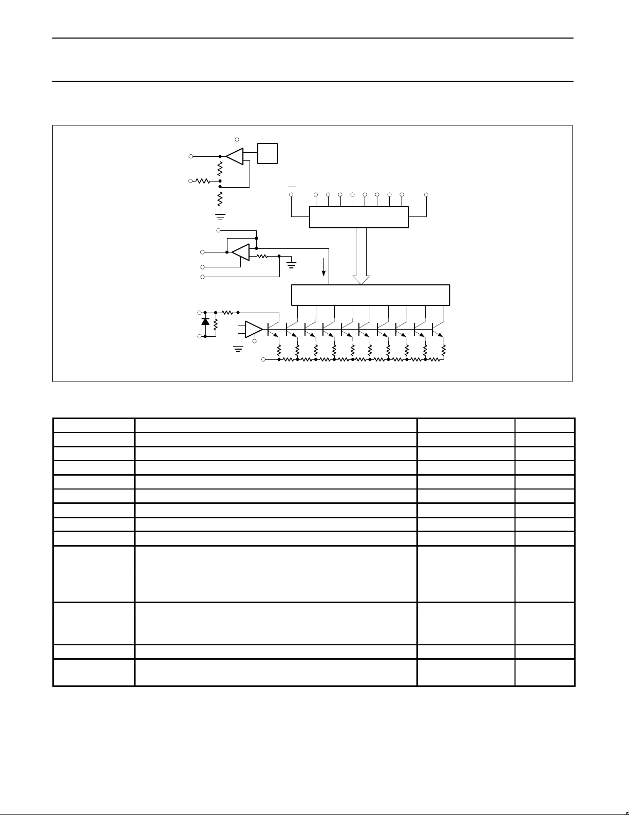
BLOCK DIAGRAM
(13)
(12)
(20)
(18)
(21)
(22)
(14)
(15)
BIPOLAR
OFFSET
V
REF
IN
ANALOG
GND
AMP
COMP
SUM
NODE
DAC CURRENT
OUTPUT
LATCHES AND
SWITCH DRIVERS
DAC SWITCHES
5k
5k
15k
(19)
(10)
MSB LSB
(1)
DIGITAL
GND5k
V
CC+
INT
V
REF
(9)
DB7
(8)
DB6
(7)
DB5
(6)
DB4
(5)
DB3
(4)
DB2
(3)
DB1
(2)
DB0
LE
V
CC–
(16)
V
OUT
5k
5k
+
–
+
–
+
–
DAC
COMP
V
REF
OUT
V
REF
ADJ
(17)
ABSOLUTE MAXIMUM RATINGS
SYMBOL PARAMETER RATING UNIT
VCC+ Positive supply voltage 18 V
VCC- Negative supply voltage -18 V
V
IN
Logic input voltage 0 to 18 V
V
REF IN
Voltage at V
REF
input 12 V
V
REF
ADJ Voltage at V
REF
adjust 0 to V
REF
V
V
SUM
Voltage at sum node 12 V
I
REF SC
Short-circuit current to ground at V
REF OUT
Continuous
I
OUTSC
Short-circuit current to ground or either supply at V
OUT
Continuous
P
D
Maximum power dissipation, TA=25°C (still-air)
1
F package 1740 mW
N package 2190 mW
D package 1600 mW
T
A
Operating temperature range
SE5018 -55 to +125 °C
NE5018 0 to +70 °C
T
STG
Storage temperature range -65 to +150 °C
T
SOLD
Lead soldering temperature
(10 seconds) 300 °C
NOTES:
1. Derate above 25°C at the following rates:
F package at 13.9mW/°C
N package at 17.5mW/°C
D package at 12.8mW/°C
Page 3
Philips Semiconductors Linear Products Product specification
NE/SE5018/50198-Bit µp-compatible D/A converter
August 31, 1994
753
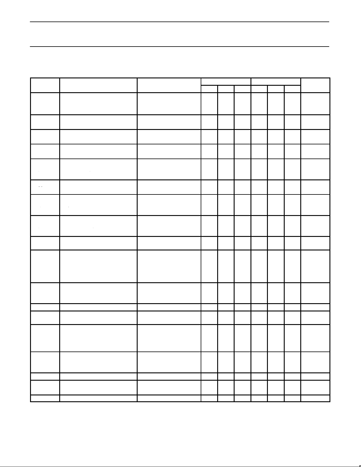
DC ELECTRICAL CHARACTERISTICS
VCC+=+15V, VCC-=-15V, SE5018. -55°C≤TA≤125°C, NE5018. 0°C≤TA≤70°C, unless otherwise specified.1 Typical values are specified at 25°C.
NE/SE5018 NE/SE5019
SYMBOL
PARAMETER
TEST CONDITIONS
Min Typ Max Min Typ Max
UNIT
Resolution 8 8 8 8 8 8 Bits
Monotonicity 8 8 8 8 8 8 Bits
Relative accuracy ±0.19 ±0.1 %FS
VCC+ Positive supply voltage 11.4 15 11.4 15 V
VCC- Negative supply voltage -11.4 -15 -11.4 -15 V
V
IN(1)
Logic “1” input voltage Pin 1=0V 2.0 2.0 V
V
IN(0)
Logic “0” input voltage Pin 1=0V 0.8 0.8 V
I
IN(1)
Logic “1” input current Pin 1=0V, 2V<VIN<18V 0.1 10 0.1 10 µA
I
IN(0)
Logic “0” input current Pin 1=0V, -5V<VIN<0.8V -2.0 -10 -2.0 -10 µA
Unipolar mode,
V
REF
=5.000V,
9.50 10.5 9.50 10.5 V
VFSFull-scale output
all bits high, TA=25°C
Bipolar mode, V
REF
=5.000V 4.75 5.25 4.75 5.25 V
+VFSFull-scale output
all bits high, TA=25°C
Bipolar mode,
V
REF
=5.000V,
-5.25
-4.75 -5.25 -4.75 V
-VFSNegative full scale
all bits low, TA=25°C
Unipolar mode,
V
REF
=5.000V
-30 +30 -30 +30 mV
VZSZero-scale Output
all bits low, TA=25°C
I
OS
Output short circuit current
TA=25°C
V
OUT
=0V
15 40 15 40 mA
PSR+
(OUT)
Output power supply
rejection (+)
V-=-15V, 13.5V≤V+≤16.5V,
external V
REF IN
=5.000V
0.001 0.01 0.001 0.01
%FS
%VS
PSR-
(OUT)
Output power supply
rejection (-)
V+=-15V, -13.5V≤V-≤-16.5V,
external V
REF IN
=5.000V
0.001 0.01 0.001 0.01
%FS
%VS
TC
FS
Full-scale temperature
coefficient
V
REF IN
=5.000V 20 20 ppm/°C
TC
ZS
Zero-scale temperature coefficient 5 5 ppm/°C
I
REF
Reference output current 3 3 mA
I
REFSC
Reference short circuit current
TA=25°C
V
REF OUT
=0V
15 30 15 30 mA
PSR+
(REF)
Reference power supply rejection
(+)
V-=-15V, 13.5V≤V+≤16.5V,
I
REF
=1.0mA
0.003 0.01 0.003 0.01 %VR/%VS
PSR-
(REF)
Reference power supply rejection
(-)
V+=-15V, -13.5V≤V-≤16.5V, 0.003 0.01 0.003 0.01 %VR/%VS
V
REF
Reference voltage I
REF
=1.0mA TA=25°C 4.9 5.0 5.25 4.9 5.0 5.25 V
TC
REF
Reference voltage temperature co-
efficient
I
REF
=1.0mA 60 60 ppm/°C
Z
IN
DAC V
REF IN
input impedance I
REF
=1.0mA, TA=25°C 4.15 5.0 5.85 4.15 5.0 5.85 kΩ
ICC+ Positive supply current VCC+=15V 7 14 7 14 mA
ICC- Negative supply current VCC-=-15V -10 -15 -10 -15 mA
P
D
Power dissipation I
REF
=1.0mA, VCC=±15V 255 435 255 435 mW
NOTES:
1. Refer to Figure 1.
V
FS
-V
FS
V
ZS
Full-scale output
Negative full scale
Zero-scale Output
Page 4
Philips Semiconductors Linear Products Product specification
NE/SE5018/50198-Bit µp-compatible D/A converter
August 31, 1994
754
AC ELECTRICAL CHARACTERISTICS
1
V
CC
= ±15V, T
A
= 25°C
NE/SE5018/19
SYMBOL
PARAMETER
TO
FROM
TEST CONDITIONS
Min Typ Max
UNIT
t
SLH
Settling time ±1/2LSB Input All bits low-to-high
2
1.8 µs
t
SHL
Settling time ±1/2LSB Input All bits high-to-low
3
2.3 µs
t
PLH
Propagation delay Output Input All bits switched low-to-high
2
300 ns
t
PHL
Propagation delay Output Input All bits switched high-to-low
3
150 ns
t
PLSB
Propagation delay Output Input 1 LSB change
2, 3
150 ns
t
PLH
Propagation delay Output LE Low-to-high transition
4
300 ns
t
PHL
Propagation delay Output LE High-to-low transition
5
150 ns
t
S
Setup time LE Input
1, 6
100 ns
t
H
Hold time Input LE
1, 6
50 ns
t
PW
Latch enable pulse width
1, 6
150 ns
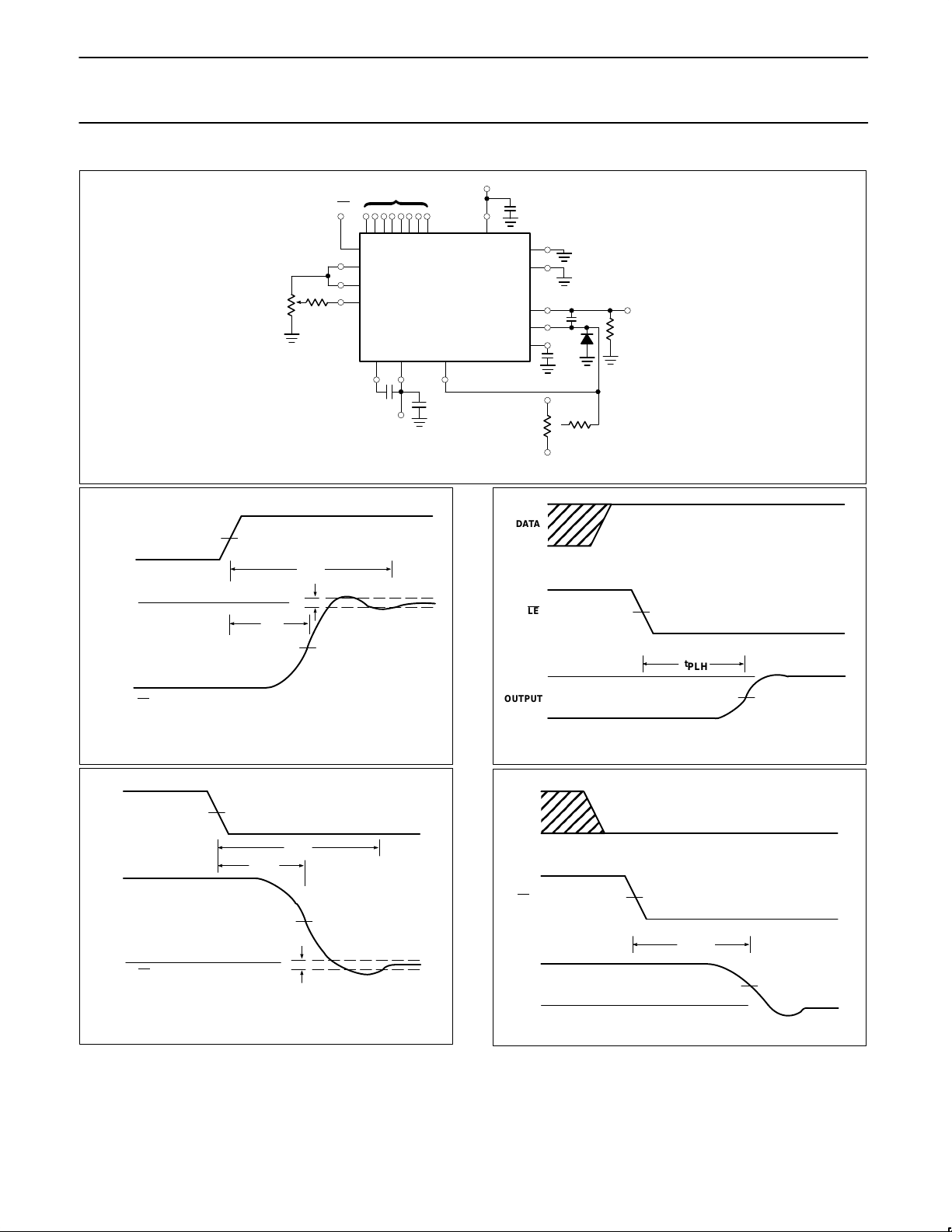
NOTES:
1. Refer to Figure 2.
2. See Figure 5.
3. See Figure 6.
4. See Figure 7.
5. See Figure 8.
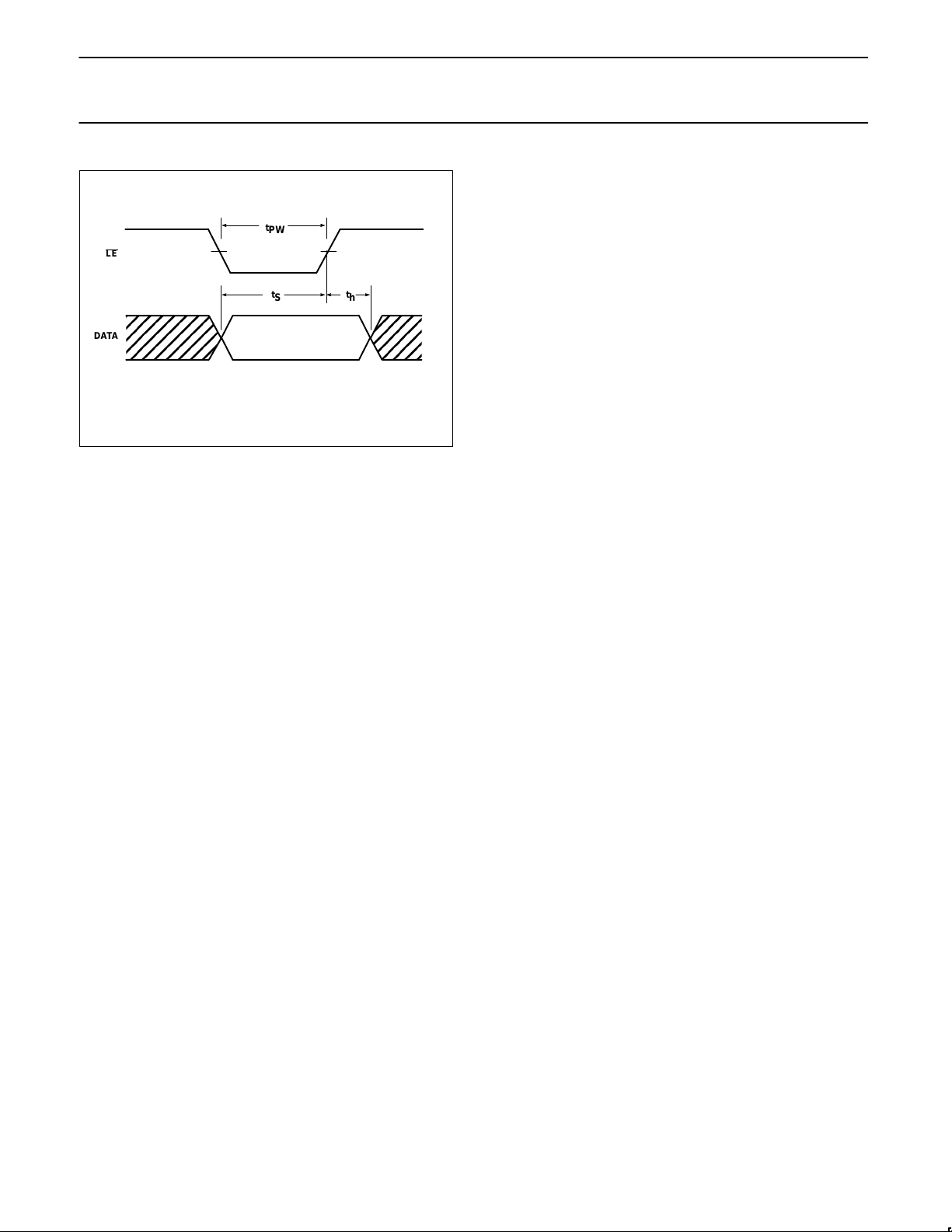
6. See Figure 9.
7. For reference currents>3mA, use of an external buffer is required.
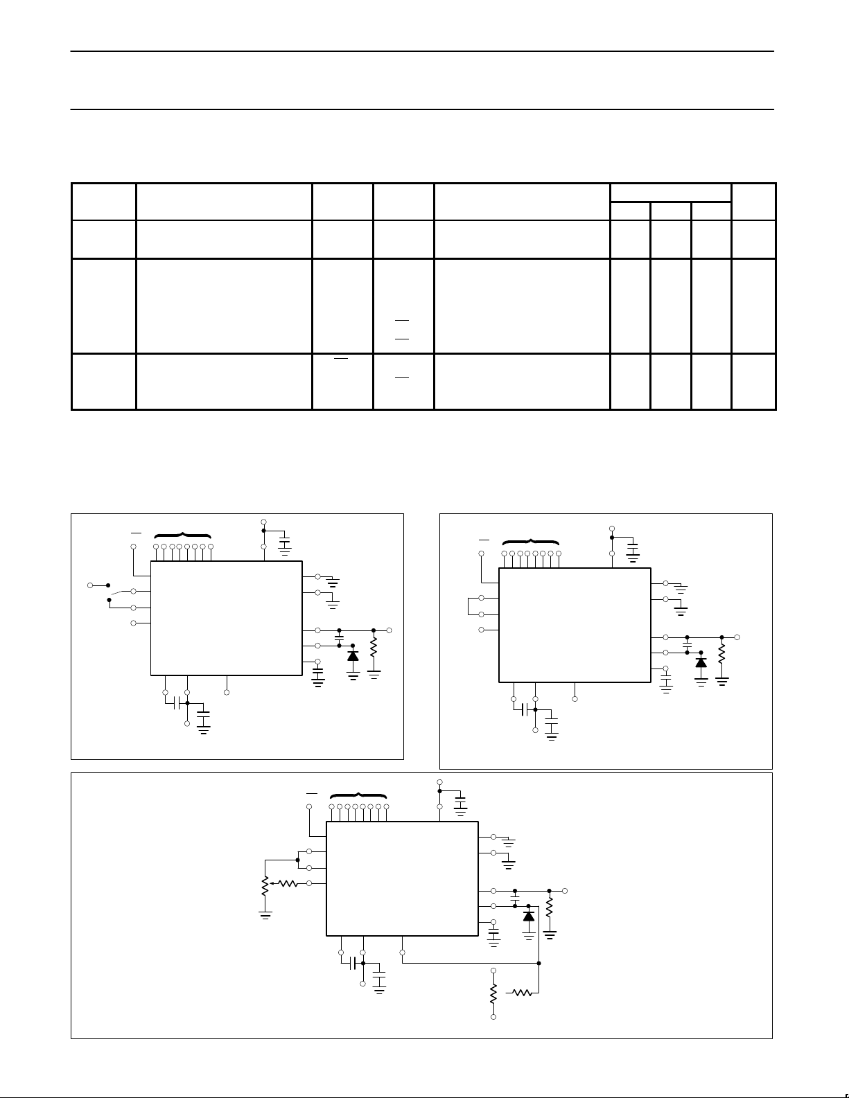
Figure 1. DC Parametric Test Configuration
0.47µF
MSB LSB
9 8 7 6 5 4 3 2 19
1
22
18
20
21
15
1716
12
13
14
10
DAC
COMP
5018
COMP
AMP
SUM
ANA GND
DIG GND
LE
V
REF
IN
V
REF
OUT
V
OUT
V
CC+
0.01µF
0.1µF
V
CC–
OUTPUT
2k
22pF
1N914
100pF
5.000V
Figure 2. AC Parametric Test Configuration
MSB LSB
9 8 7 6 5 4 3 2 19
1
22
18
20
21
15
1716
12
13
14
10
DAC
COMP
5018
COMP
AMP
SUM
ANA GND
DIG GND
OUTPUT
2k
22pF
1N914
100pF
0.47µF
LE
V
OUT
V
CC+
0.01µF
0.1µF
V
CC–
V
REF
IN
Figure 3. Full-/Zero-Scale Adjust — Unipolar Output (0–10V)
0.47µF
MSB LSB
10k
10T
80k
9 8 7 6 5 4 3 2 19
1
22
18
20
21
15
1716
12
13
14
10
DAC
COMP
5018
COMP
AMP
SUM
ANA GND
DIG GND
LE
V
REF
OUT
V
REF
ADJ
V
OUT
V
CC+
0.01µF
0.1µF
V
CC–
OUTPUT
2k
22pF
1N914
100pF
1M
V
CC+
20k
10T
ZERO SCALE
ADJUST
V
CC–
FULL SCALE
ADJUST
Page 5
Philips Semiconductors Linear Products Product specification
NE/SE5018/50198-Bit µp-compatible D/A converter
August 31, 1994
755
0.47µF
Figure 4. Bipolar Output Operation (–5 to +5V)
MSB LSB
10k
10T
80k
9 8 7 6 5 4 3 2 19
1
22
18
20
21
15
1716
12
13
14
10
DAC
COMP BIP OFFSET
5018
COMP
AMP
SUM
ANA GND
DIG GND
LE
V
REF
IN
V
REF
OUT
V
REF
ADJ
V
OUT
V
CC+
0.01µF
0.1µF
V
CC–
OUTPUT
2k
22pF
1N914
100pF
1M
V
CC+
20k
10T
ZERO SCALE
ADJUST
V
CC–
OUTPUT
Figure 5. Settling Time and Propagation Delay,
Low-to-High Data
t
SLH
t
PLH
1LSB
DATA
10V
0V
LE
= LOW
Figure 6. Settling Time and Propagation Delay,
High-to-Low Data
LE = LOW
t
SHL
OUTPUT
10V
0V
1LSB
t
PHL
DATA
Figure 7. Propagation Delay, Latch Enable to Output
LE
DATA
t
PLH
OUTPUT
10V
0V
Figure 8. Propagation Delay, Latch Enable to Output
LE
DATA
t
PHL
t
PHL
OUTPUT
10V
0V
Page 6
Philips Semiconductors Linear Products Product specification
NE/SE5018/50198-Bit µp-compatible D/A converter
August 31, 1994
756
Figure 9. Latch Pulse Width, Setup and Hold Times
LE
DATA
t
PW
t
S
t
h
 Loading...