

Page 1

INTEGRATED CIRCUITS
SCN68562
Dual universal serial communications
controller (DUSCC)
Product specification
IC19 Data Handbook
1995 May 01
Page 2

Philips Semiconductors Product specification
SCN68562Dual universal serial communications controller (DUSCC)
DESCRIPTION
The Philips Semiconductors SCN68562 Dual Universal Serial
Communications Controller (DUSCC) is a single-chip MOS-LSI
communications device that provides two independent,
multi-protocol, full-duplex receiver/transmitter channels in a single
package. It supports bit-oriented and character-oriented (byte count
and byte control) synchronous data link controls as well as
asynchronous protocols. The SCN68562 interfaces to the 68000
MPUs via asynchronous bus control signals and is capable of
program-polled, interrupt driven, block-move or DMA data transfers.
The operating mode and data format of each channel can be
programmed independently.
Each channel consists of a receiver, a transmitter, a 16-bit
multifunction counter/timer, a digital phase-locked loop (DPLL), a
parity/CRC generator and checker, and associated control circuits.
The two channels share a common bit rate generator (BRG),
operating directly from a crystal or an external clock, which provides
16 common bit rates simultaneously. The operating rate for the
receiver and transmitter of each channel can be independently
selected from the BRG, the DPLL, the counter/timer, or from an
external 1X or 16X clock, making the DUSCC well suited for
dual-speed channel applications. Data rates up to 4Mbits per
second are supported.
PIN CONFIGURATIONS
N PACKAGE
IACKN
RTxDAKBN/
GPI1BN
IRQN
RESETN
RTSBN/
SYNOUTBN
TRxCB
RTxCB
DCDBN/
SYNIBN
RxDB
TxDB
TxDAKBN/
GPI2BN
RTxDRQBN/
GPO1BN
TxDRQBN/
GPO2BN/RTSBN
CTSBN/LCBN
DTACKN
DTCN
GND
1
2
A3
3
A2
4
A1
5
6
7
8
9
10
11
12
13
14
15
16
17
18
D7
19
D6
20
D5
21
D4
22
23
24
DIP
48
V
DD
47
A4
46
A5
45
A6
RTxDAKAN/
44
GPI1AN
43
X1/CLK
42
X2/IDCN
RTSAN/
41
SYNOUTAN
40
TRxCA
39
RTxCA
DCDAN/
38
SYNIAN
37
Rxda
36
TxDA
TxDAKAN/
35
GPI2AN
RTxDRQAN/
34
GPO1AN
TxDRQAN/
33
GPO2AN/RTSAN
32
CTSAN/LCAN
31
D0
30
D1
29
D2
28
D3
27
DONEN
26
R/WN
25
CSN
The transmitter and receiver each contain a four-deep FIFO with
appended transmitter command and receiver status bits and a shift
register. This permits reading and writing of up to four characters at
a time, minimizing the potential of receiver overrun or transmitter
underrun, and reducing interrupt or DMA overhead. In addition, a
flow control capability is provided to disable a remote transmitter
when the FIFO of the local receiving device is full.
Two modem control inputs (DCD and CTS) and three modem
control outputs are provided. These inputs and outputs can be
optionally programmed for other functions.
FEA TURES
General Features
•Dual full-duplex synchronous/asynchronous receiver and
transmitter
•Multiprotocol operation
– BOP: HDLC/ADCCP, SDLC, SDLC loop, X.25 or X.75 link level,
etc.
– COP: BISYNC, DDCMP
– ASYNC: 5–8 bits plus optional parity
•Four character receiver and transmitter FIFOs
INDEX
CORNER
Pin Function Pin Function
1 IACKN 27 CSN
2 A3 28 R/WN
3 A2 29 DONEN
4A1 30D3
5 RTxDAKBN/ 31 D2
6 IRQN 33 D0
7NC 34NC
8 RESETN 35 CTSAN/LCAN
9 RTSBN/ 36 TxDRQAN/
10 TRxCB 37 RTxDRQAN/
11 RTxCB GPO1AN
12 DCDBN/ 38 TxDAKAN/
13 NC 39 TxDA
14 RxDB 40 RxDA
15 TxDB 41 NC
16 TxDAKBN/ 42 DCDAN/
17 RTxDRQBN/ 43 RTxCA
18 TxDRQBN/ 45 RTSAN/
19 CTSBN/LCBN 46 X2/IDCN
20 D7 47 X1/CLK
21 D6 48 RTxDAKAN/
22 D5 GPI1AN
23 D4 49 A6
24 DTACKN 50 A5
25 DTCN 51 A4
26 GND 52 V
A PACKAGE
7
8
PLCC
20
21
TOP VIEW
GPI1BN 32 D1
SYNOUTBN GPO2AN/RTSAN
SYNIBN GPI2AN
GPI2BN SYNIAN
GPO1BN 44 TRxCA
GPO2BN/RTSBN SYNOUTAN
47
1
46
34
33
DD
SD00222
Figure 1. Pin Configurations
1995 May 01 853-0831 15179
2
Page 3

Philips Semiconductors Product specification
SCN68562Dual universal serial communications controller (DUSCC)
•0 to 4MHz data rate
•Programmable bit rate for each receiver and transmitter selectable
from:
– 16 fixed rates: 50 to 38.4k baud
– One user-defined rate derived from programmable
counter/timer
– External 1X or 16X clock
– Digital phase-locked loop
•Parity and FCS (frame check sequence LRC or CRC) generation
and checking
•Programmable data encoding/decoding: NRZ, NRZI, FM0, FM1,
Manchester
•Programmable channel mode: full- and half-duplex, auto-echo, or
local loopback
•Programmable data transfer mode: polled, interrupt, DMA, wait
•DMA interface
– Compatible with the Philips Semiconductors SCB68430 Direct
Memory Access Interface (DMAI) and other DMA controllers
– Single- or dual-address dual transfers
– Half- or full-duplex operation
– Automatic frame termination on counter/timer terminal count or
DMA DONE
•Interrupt capabilities
– Daisy chain option
– Vector output (fixed or modified by status)
– Programmable internal priorities
– Maskable interrupt conditions
•Multi-function programmable 16-bit counter/timer
– Bit rate generator
– Event counter
– Count received or transmitted characters
– Delay generator
– Automatic bit length measurement
•Modem controls
– RTS, CTS, DCD, and up to four general I/O pins per channel
– CTS and DCD programmable autoenables for Tx and Rx
– Programmable interrupt on change of CTS or DCD
•On-chip oscillator for crystal
•TTL compatible
•Single +5V power supply
Asynchronous Mode Features
•Character length: 5 to 8 bits
•Odd or even parity, no parity, or force parity
•Up to two stop bits programmable in 1/16-bit increments
•1X or 16X Rx and Tx clock factors
•Parity, overrun, and framing error detection
•False start bit detection
•Start bit search 1/2-bit time after framing error detection
•Break generation with handshake for counting break characters
•Detection of start and end of received break
•Character compare with optional interrupt on match
•Transmits up to 4Mbs and receive up to 2Mbps data rates
Character-Oriented Protocol Features
•Character length: 5 to 8 bits
•Odd or even parity, no parity, or force parity
•LRC or CRC generation and checking
•Optional opening PAD transmission
•One or two SYN characters
•External sync capability
•SYN detection and optional stripping
•SYN or MARK line-fill on underrun
•Idle in MARK or SYNs
•Parity, FCS, overrun, and underrun error detection
BISYNC Features
– EBCDIC or ASCII header, text and control messages
– SYN, DLE stripping
– EOM (end of message) detection and transmission
– Auto transparent mode switching
– Auto hunt after receipt of EOM sequence (with closing PAD
check after EOT or NAK)
– Control character sequence detection for both transparent and
normal text
Bit-Oriented Protocol Features
•Character length: 5 to 8 bits
•Detection and transmission of residual character: 0–7 bits
•Automatic switch to programmed character length for 1 field
•Zero insertion and deletion
•Optional opening PAD transmission
•Detection and generation of FLAG, ABORT, and IDLE bit patterns
•Detection and generation of shared (single) FLAG between
frames
•Detection of overlapping (shared zero) FLAGs
•ABORT, ABORT-FLAGs, or FCS FLAGs line-fill on underrun
•Idle in MARK or FLAGs
•Secondary address recognition including group and global
address
•Single- or dual-octet secondary address
•Extended address and control fields
•Short frame rejection for receiver
•Detection and notification of received end of message
•CRC generation and checking
•SDLC loop mode capability
1995 May 01
3
Page 4

Philips Semiconductors Product specification
DESCRIPTION
DWG #
SCN68562Dual universal serial communications controller (DUSCC)
ORDERING INFORMATION
VCC = +5V +5%, TA = 0°C to +70°C
Serial Data Rate = 4Mbps Maximum
48-Pin Plastic Dual In-Line Package (DIP) SCN68562C4N48 SOT240-1
52-Pin Plastic Leaded Chip Carrier (PLCC) Package SCN68562C4A52 SOT238-3
NOTE: See SCN26562/SCN68562 User’s Guide for detailed description of all the features.
BLOCK DIAGRAM
DTACKN
RWN
A1-A6
CSN
RESETN
RTxDRQAN/GPO1AN
RTxDRQBN/GPO1BN
TxDRQAN/GPO2AN
TxDRQBN/GPO2BN
RTxDAKAN/GPI1AN
RTxDAKBN/GPI1BN
TxDAKAN/GPI2AN
TxDAKBN/GPI2BN
DTCN
DONEN
TRxCA/B
RTxCA/B
RTSBN/SYNOUTBN
RTSAN/SYNOUTAN
CTSA/BN
DCDBN/SYNIBN
DCDAN/SYNIAN
D0-D7
MPU
INTERFACE
DMA INTERFACE
SPECIAL
FUNCTION
PINS
BUS
BUFFER
INTERFACE/
OPERATION
CONTROL
ADDRESS
DECODE
R/W
DECODE
DMA
CONTROL
CCRA/B
PCRA/B
RSRA/B
TRSRA/B
ICTSRA/B
GSR
CMR1A/B
CMR2A/B
OMRA/B
CONTROL
INTERNAL BUS
CHANNEL MODE
AND TIMING A/B
DPLL CLK
MUX A/B
DPLL A/B
BRG
COUNTER/
TIMER A/B
C/T CLK
MUX A/B
CTCRA/B
CTPRHA/B
CTPRLA/B
CTHA/B
CTLA/B
TRANSMIT A/B
TRANS CLK
MUX
TPRA/B
TTRA/B
TX SHIFT
REG
TRANSMIT
4 DEEP
FIFO
CRC
GEN
SPEC CHAR
GEN LOGIC
TxD A/B
1995 May 01
IRQN
IACKN
X1/CLK
X2/IDCN
INTERRRUPT
CONTROL
ICRA/B
IERA/B
IVR
IVRM
OSCILLATOR
DUSCC
LOGIC
Figure 2. Block Diagram
4
RECEIVER A/B
RCVR CLK
MUX
RPRA/B
RTRA/B
S1RA/B
S2RA/B
RCVR
SHIFT REG
RECEIVER
4 DEEP
FIFO
CRC
ACCUM
BISYNC
COMPARE
LOGIC
RxD A/B
SD00223
Page 5

Philips Semiconductors Product specification
SCN68562Dual universal serial communications controller (DUSCC)
PIN DESCRIPTION
In this data sheet, signals are discussed using the terms ‘active’ and ‘inactive’ or ‘asserted’ and ‘negated’ independent of whether the signal is
active in the High (logic 1) or Low (logic 0) state. N at the end of a pin name signifies the signal associated with the pin is active-Low (see
individual pin description for the definition of the active level of each signal.) Pins which are provided for both channels are designated by A/B
after the name of the pin and the active-Low state indicator, N, if applicable. A similar method is used for registers provided for both channels:
these are designated by either an underline or by A/B after the name.
MNEMONIC
A1 – A6 4-2,
D0 – D7 31-28,
R/WN 26 I Read/Write: A High input indicates a read cycle and a Low input indicates a write cycle
CSN 25 I Chip Select: Active-Low input. When Low, data transfers between the CPU and the
DTACKN 22 O Data Transfer Acknowledge: Active-Low, 3-State. DTACKN is asserted on a write cycle
IRQN 6 O Interrupt Request: Active-Low, open-drain. This output is asserted upon occurrence of
IACKN 1 I Interrupt Acknowledge: Active-Low. When IACKN is asserted, the DUSCC responds by
X1/CLK 43 I Crystal or External Clock: When using the crystal oscillator, the crystal is connected
X2/IDCN 42 O Crystal or Interrupt Daisy Chain: When a crystal is used as the timing source, the
RESETN 7 I Master Reset: Active-Low. A low on this pin resets the transmitters and receivers and
RxDA, RxDB 37, 12 I Channel A (B) Receiver Serial Data Input: The least significant bit is received first. If
TxDA, TxDB 36, 13 O Channel A (B) Transmitter Serial Data Output: The least significant bit is transmitted
RTxCA, RTxCB 39, 10 I/O Channel A (B) Receiver/Transmitter Clock: As an input, it can be programmed to
DIP
PIN NO.
45-47
21-18
TYPE NAME AND FUNCTION
I Address Lines: Active-High. Address inputs which specify which of the internal registers
is accessed for read/write operation.
I/O Bidirectional Data Bus: Active High, 3-State. Bit 0 is the LSB and bit 7 is the MSB. All
data, command, and status transfers between the CPU and the DUSCC take place over
this bus. The data bus is enabled when CSN is Low, during interrupt acknowledge cycles
and single-address DMA acknowledge cycles.
when a cycle is initiated by assertion of the CSN input.
DUSCC are enabled on D0 – D7 as controlled by the R/WN and A1 – A6 inputs. When
CSN is High, the DUSCC is isolated from the data bus (except during interrupt
acknowledge cycles and single-address DMA transfers) and D0 – D7 are placed in the
3-State condition.
to indicate that the data on the bus has been latched, and on a read cycle or interrupt
acknowledge cycle to indicate valid data is on the bus. The signal is negated when
completion of the cycle is indicated by negation of the CSN or IACKN input, and returns to
the inactive state (3-State) a short period after it is negated. In a single address DMA
mode, data is latched with the falling edge of DTCN. DTACKN is negated when
completion of the cycle is indicated by the assertion of DTCN or negation of DMA
acknowledge inputs (whichever occurs first), and returns to the inactive state (3-State) a
short period after it is negated. When negated, DTACKN becomes an open-drain output
and requires an external pull-up resistor.
any enabled interrupting condition. The CPU can read the general status register to
determine the interrupting condition(s), or can respond with an interrupt acknowledge cycle
to cause the DUSCC to output an interrupt vector on the data bus.
placing the contents of the interrupt vector register (modified or unmodified by status) on
the data bus and asserting DTACKN. If no active interrupt is pending, DTACKN is not
asserted.
between pins X1 and X2. If a crystal is not used, and external clock is supplied at this
input. This clock is used to drive the internal bit rate generator, as an optional input to the
counter/timer or DPLL, and to provide other required clocking signals.
crystal is connected between pins X1 and X2. This pin can be programmed to provide and
interrupt daisy chain active-Low output which propagates the IACKN signal to lower priority
devices, if no active interrupt is pending. This pin should be grounded when an external
clock is used on X1 and X2, is not used as an interrupt daisy chain output.
resets the registers shown in Table 1 of the CDUSCC Users’ Guide. Reset in
asynchronous, i.e., no clock is required.
external receiver clock is specified for the channel, the input is sampled on the rising edge
of the clock.
first. This output is held in the marking (High) condition when the transmitter is disabled or
when the channel is operating in local loopback mode. If external transmitter clock is
specified for the channel, the data is shifted on the falling edge of the clock.
supply the receiver, transmitter, counter/timer, or DPLL clock. As an output, can supply the
counter/timer output, the transmitter shift clock (1X), or the receiver sampling clock (1X).
The maximum external receiver/transmitter clock frequency is 4MHz.
1995 May 01
5
Page 6

Philips Semiconductors Product specification
SCN68562Dual universal serial communications controller (DUSCC)
PIN DESCRIPTION (Continued)
MNEMONIC
TRxCA, TRxCB 40, 9 I/O Channel A (B) Transmitter/Receiver Clock: As an input, it can supply the receiver,
CTSA/BN, LCA/BN 32, 17 I/O Channel A (B) Clear-To-Send Input or Loop Control Output: Active-Low. The signal
DCDA/BN,
SYNIA/BN
RTxDRQA/BN,
GPO1A/BN
TxDRQA/BN,
GPO2A/BN,
RTSA/BN
RTxDAKA/BN,
GPI1A/BN
TxDAKA/BN,
GP12A/BN
DTCN 23 I Device Transfer Complete: Active-Low. DTCN is asserted by the DMA controller to
DONEN 27 I/O Done: Active-Low, open-drain. See Detailed Operation for a description of the function of
RTSA/BN,
SYNOUTA/BN
V
DD
GND 24 I Signal and power ground input.
DIP
PIN NO.
38, 11 I Channel A (B) Data Carrier Detected or External Sync Input: The function of this pin is
34, 15 O Channel A (B) Receiver/T ransmitter DMA Service Request or General Purpose
33, 16 O Channel A (B) Transmitter DMA Service Request, General Purpose Output, or
44, 5 I Channel A (B) Receiver/Transmitter DMA Acknowledge or General Purpose Input:
35, 14 I Channel A (B) Transmitter DMA Acknowledge or General Purpose Input: Active-Low.
41, 8 O Channel A (B) Sync Detect or Request-to-Send: Active-Low. If programmed as a sync
48 I +5V + 10% power input.
TYPE NAME AND FUNCTION
transmitter, counter/timer, or DPLL clock. As an output, it can supply the counter/timer
output, the DPLL output, the transmitter shift clock (1X), the receiver sampling clock (1X),
the transmitter BRG clock (16X), The receiver BRG clock (16X), or the internal system
clock (X1/2). The maximum external receiver/transmitter clock frequency is 4MHz.
can be programmed to act as an enable for the transmitter when not in loop mode. The
DUSCC detects logic level transitions on this input and can be programmed to generate an
interrupt when a transition occurs. When operating in the COP loop mode, this pin
becomes a loop control output which is asserted and negated by DUSCC commands.
This output provides the means of controlling external loop interface hardware to go on-line
and off-line without disturbing operation of the loop.
programmable. As a DCD active-Low input, it acts as an enable for the receiver or can be
used as a general purpose input for the DCD function, the DUSCC detects logic level
transitions on this input and can be programmed to generate an interrupt when a transition
occurs. As an active-Low external sync input, it is used in COP modes to obtain character
synchronization without receipt of a SYN character. This mode can be used in disc or
tape controller applications or for the optional byte timing lead in X.21.
Output: Active-Low. For half-duplex DMA operation, this output indicates to the DMA
controller that one or more characters are available in the receiver FIFO (when the
receiver is enabled) or that the transmit FIFO is not full (when the transmitter is enabled).
For full-duplex DMA operation, this output indicates to the DMA controller that data is
available in the receiver FIFO. In non-DMA mode, this pin is a general purpose output that
can be asserted and negated under program control.
Request-to-Send: Active-Low. For full-duplex DMA operation, this output indicates to the
DMA controller that the transmit FIFO is not full and can accept more data. When not in
full-duplex DMA mode, this pin can be programmed as a general purpose or a Request-to
-Send output, which can be asserted and negated under program control (see Detailed
Operation).
Active-Low. For half-duplex single address DMA operation, this input indicates to the
DUSCC that the DMA controller has acquired the bus and that the requested bus cycle
(read receiver FIFO or load transmitter FIFO) is beginning. For full-duplex single address
DMA operation, this input indicates to the DUSCC that the DMA controller has acquired
the bus and that the requested read receiver FIFO bus cycle is beginning. Because the
state of this input can be read under program control, it can be used as a general purpose
input when not in single address DMA mode.
When the channel is programmed for full-duplex single address DMA operation, this input
is asserted to indicate to the DUSCC that the DMA controller has acquired the bus and
that the requested load transmitter FIFO bus cycle is beginning. Because the state of this
input can be read under program control, it can be used as a general purpose input when
not in full-duplex single address DMA mode.
indicate that the requested data transfer is complete.
this pin.
output, it is asserted one bit time after the specified sync character (COP or BISYNC
modes) or a FLAG (BOP modes) is detected by the receiver. As a Request-to-Send
modem control signal, it functions as described previously for the TxDRQN/RTSN pin.
1995 May 01
6
Page 7
Philips Semiconductors Product specification
SYMBOL
PARAMETER
TEST CONDITIONS
UNIT
SCN68562Dual universal serial communications controller (DUSCC)
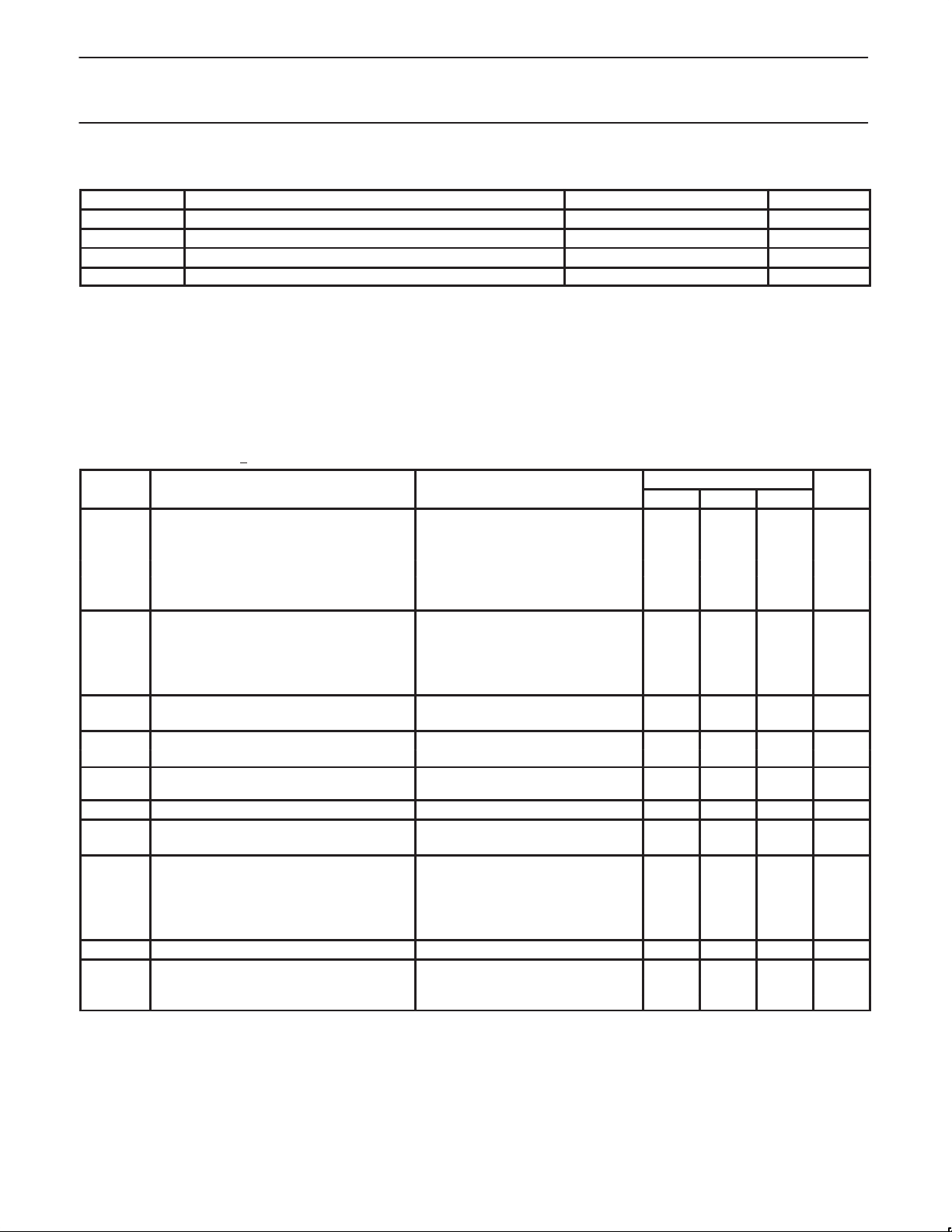
ABSOLUTE MAXIMUM RATINGS
SYMBOL
T
T
V
V
A
STG
CC
S
Operating ambient temperature
Storage Temperature -65 to +150 °C
Voltage from VCC to GND
Voltage from any pin to ground
1
PARAMETER RATING UNIT
2
3
3
0 to +70 °C
-0.5 to +7.0 V
-0.5 to VCC +0.5 V
NOTES:
1. Stresses above those listed under Absolute Maximum Ratings may cause permanent damage to the device. This is a stress rating only and
functional operation of the device at these or any other conditions above those indicated in the operation section of this specification is not
implied.
2. For operating at elevated temperatures, the device must be derated based on +150°C maximum junction temperature and thermal
resistance of 40°C/W for plastic DIP and 42°C/W for PLCC.
3. This product includes circuitry specifically designed for the protection of its internal devices from damaging effects of excessive static
charge. Nonetheless, it is suggested that conventional precautions be taken to avoid applying any voltages larger than the rated maxima.
DC ELECTRICAL CHARACTERISTICS
= 0 to +70°C, VCC = 5.0V + 5%
T
A
1, 4
LIMITS
Min Typ Max
V
IL
Input low voltage:
All except X1/CLK 0.8 V
X1/CLK 0.4 V
V
IH
Input high voltage:
All except X1/CLK 2.0 V
X1/CLK 2.4 V
V
OL
Output low voltage:
CC
V
All except IRQN, DONEN IOL = 5.3mA 0.5 V
IRQN, DONEN IOL = 8.8mA 0.5 V
V
OH
Output high voltage:
(Except open drain outputs) IOH = -400µA 2.4 V
I
ILX1
I
IHX1
I
ILX2
I
IHX2
I
IL
I
L
I
OZH
I
OZL
ODL
I
X1/CLK input low current
X1/CLK input high current
X2 input low current
X2 input high current
Input low current
DTCN, TxDAKA/BN, RTxDAKA/BN VIN = 0 -40 µA
Input leakage current VIN = 0 to V
Output off current high, 3-State data bus VIN = V
Output off current low , 3-State data bus VIN = 0 -5 µA
Open drain output low current in off VIN = 0
3
3
3
3
VIN = 0, X2 = GND -5.5 0.0 mA
VIN = VCC, X2 = GND 1.0 mA
VIN = 0, X1 = open -100 µA
VIN = VCC, X1 = open 100 µA
CC
CC
-5 5 µA
5 µA
state: DONEN -120 -25 µA
IRQN, DTACKN -5 µA
I
ODH
Open drain output high current in off VIN = V
CC
state: DONEN, IRQN, DTACKN 5 µA
I
C
C
C
CC
IN
OUT
I/O
Power supply current VO = 0 to V
Input capacitance
Output capacitance
Input/output capacitance
2
2
2
VCC = GND = 0 10 pF
VCC = GND = 0 15 pF
VCC = GND = 0 20 pF
CC
275 mA
NOTES:
1. Parameters are valid over specified temperature and voltage range.
2. These values were not explicitly tested; they are guaranteed by design and characterization data.
3. X1/CLK and X2 are not tested with a crystal installed.
4. This specification applies to revision D, revision E and later revisions.
1995 May 01
7
Page 8

Philips Semiconductors Product specification
NO.FIGURE
PARAMETER
UNIT
SCN68562Dual universal serial communications controller (DUSCC)
AC ELECTRICAL CHARACTERISTICS
1, 2, 3, 4
TA = -55 to +110°c, VCC = 5V + 10%
LIMITS
Min Typ Max
1 3 RESETN pulse width 1.2 µS
2 4,6 A1 - A6 set-up time to CSN Low 10 nS
3 4,6 A1 - A6 hold time from CSN High 0 nS
4 4,6 RWN set-up time to CSN Low 0 nS
5 4,6 RWN hold time to CSN High 0 nS
6 4,6 CSN High pulse width
4
160 nS
7 4,5 CSN or IACKN High from DTACKN Low 30 nS
7A 5 IACKN High to DTACKN High 200 nS
8 4,5 Data valid from CSN or IACKN Low 300 nS
9 4 Data bus floating from CSN High
10 6 Data hold time from DTACKN Low
7
5
0 nS
100 nS
11 4,6 DTACKN Low from read data ready 0 nS
12 4,6 DTACKN Low from CSN Low 560 nS
12A 6 CSN Low to write data valid 50 nS
13 4,6 DTACKN High from CSN High 150 nS
14 4,6 DTACKN high impedance from CSN High 185 nS
15 5 DTACKN Low from IACKN Low 550 nS
16 8 GPI input set-up time to CSN Low 20 nS
17 8 GPI input hold time from CSN Low 100 nS
18 8 GPO output valid from DTACKN Low 300 nS
19 9 IRQN High from:
Read RxFIFO (RxRDY interrupt) 450 nS
Write TxFIFO (TxRDY interrupt)
Write RSR (Rx condition interrupt)
Write TRSR (Rx/Tx interrupt)
Write ICTSR (port change and CT int.)
8
8
8
8
450 nS
400 nS
400 nS
400 nS
20 10 X1/CLK High or Low time 25 nS
X1/CLK frequency 2.0 14.7456 16 MHz
CTCLK High or Low time 100 nS
CTCLK frequency 0 4 MHz
RxC High or Low time 110 nS
RxC frequency (16X or 1X)
9
0 4 MHz
TxC High or Low time 110 nS
TxC frequency (16X or 1X) 0 4 MHz
21 11 TxD output from TxC input Low (1X)
(16X)
240
435
22 11 TxD output from TxC output Low 50 nS
23 12 RxD data set-up time to RxC High 50 nS
24 12 RxD data hold time from RxC High 50 nS
25 13 IACKN Low to daisy chain Low 200 nS
26 15 Data valid from receive DMA ACKN 300 nS
27 14,15 DTCN width 100 nS
28 14,15 RDYN Low to DTCN Low 80 nS
29 15 Data bus float from DTCN Low
7
200 nS
30 14,15 DMA ACKN Low to RDYN (DTACKN) Low 360 nS
31 14,15 RDYN High from DTCN Low 230 nS
32 14,15 RDYN High impedance from DTCN Low 250 nS
33 15 Receive DMA REQN High from DMA ACKN Low 325 nS
34 15 Receive DMA ACKN width 150 nS
35 14,15 Receive DMA ACKN Low to DONEN Low 250 nS
36 14 Data set-up to DTCN Low 50 nS
37 14 Data hold from DTCN Low
6
50 nS
38 14 Transmit DMA REQN High from ACKN Low 340 nS
39 14 Transmit DMA ACKN width 150 nS
40 14 Transmit DMA ACKN Low to DONEN Low output 250 nS
40A 14 DTCN Low DONEN output High 260 nS
41 16 CSN Low to transmit DONEN Low output 300 nS
nS
nS
1995 May 01
8
Page 9
Philips Semiconductors Product specification
SCN68562Dual universal serial communications controller (DUSCC)
NO. UNIT
NO. UNIT
PARAMETERFIGURE
PARAMETERFIGURE
LIMITS
MaxTypMin
42 16 CSN Low to transmit DMA REQ negated 400 nS
43 16 CSN Low to receive DONEN Low 300 nS
44 16 CSN Low to receive DMA REQ negated 400 nS
NOTES:
1. Parameters are valid over specified temperature range.
2. All voltage measurements are referenced to ground (GND). For DC and functional testing, all inputs except X1/CLK swing between 0.8V and
2.0V with a transition time of 20ns maximum. For X1/CLK, this swing is between 0.4V and 2.4V All time measurements are referenced at
input voltages of 0.4V and 2.4V for all inputs. Output levels are referenced at 1.2V and 2.0V, as appropriate.
3. Test conditions for outputs: C
= 150pF, except open-drain outputs. Test condition for open-drain outputs: C
L
= 50pF to GND, RL = 2.7kΩ to V
L
CC
except DTACKN whose RL = 820Ω to VCC and CL = 150pF to GND and DONEN which requires CL = 50pF to GND and RL = 1kΩ to VCC.
4. This specification will impose maximum 68000 CPU CLK to 6MHz. Higher CPU CLK can be used if repeating bus cycles are not performed.
5. Execution of the valid command (after it is latched) requires three falling edges of X1 (see Figure 14).
6. In single address DMA mode write operation, data is latched by the falling edge of DTCN.
7. These values were not explicitly tested, they are guaranteed by design and characterization data.
8. These timings are from the falling edge of DTACKN (not CSN rising).
9. X1/CLK frequency must be at least four times the receiver serial data rate.
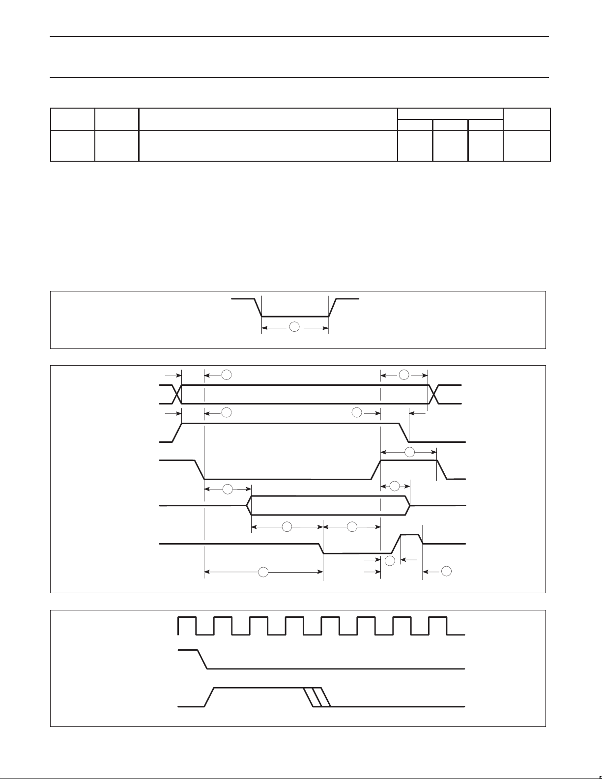
RESETN
1
SD00224
Figure 3. Reset Timing
2 3
A1–A6
R/WN
CSN
D0–D7
DTACKN
COMMAND
X1/CLK
DTACKN
VALID
8
11 7
12
Figure 4. Bus Timing (Read Cycle)
54
6
9
13
14
SD00225
1995 May 01
SD00226
Figure 5. Command Timing
9
Page 10
Philips Semiconductors Product specification
SCN68562Dual universal serial communications controller (DUSCC)
A1–A6
RWN
CSN
D0–D7
DTACKN
IRQN
12A
2
4
12
7
13
3
5
6
10
14
SD00228
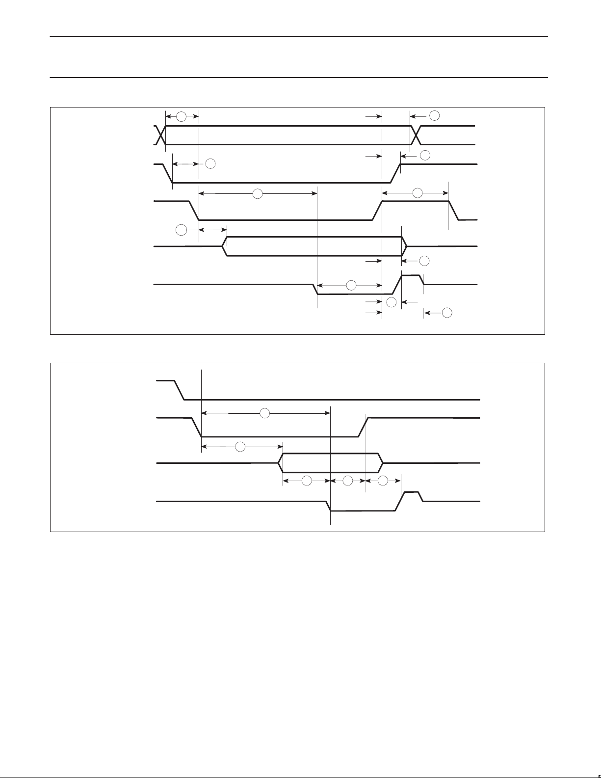
Figure 6. Bus Timing (Write Cycle)
IACKN
D0–D7
DTACKN
15
8
11 7 7A
SD00229
Figure 7. Interrupt Cycle Timing
1995 May 01
10
Page 11
Philips Semiconductors Product specification
SCN68562Dual universal serial communications controller (DUSCC)
RWN
CSN
GPI1N
AND/OR GPI2N
RWN
CSN
GPO1N
AND/OR GPO2N
16
OLD DATA
17
18
NEW DATA
X1/CLK
CTCLK
RxC
TxC
DTACK
SD00230
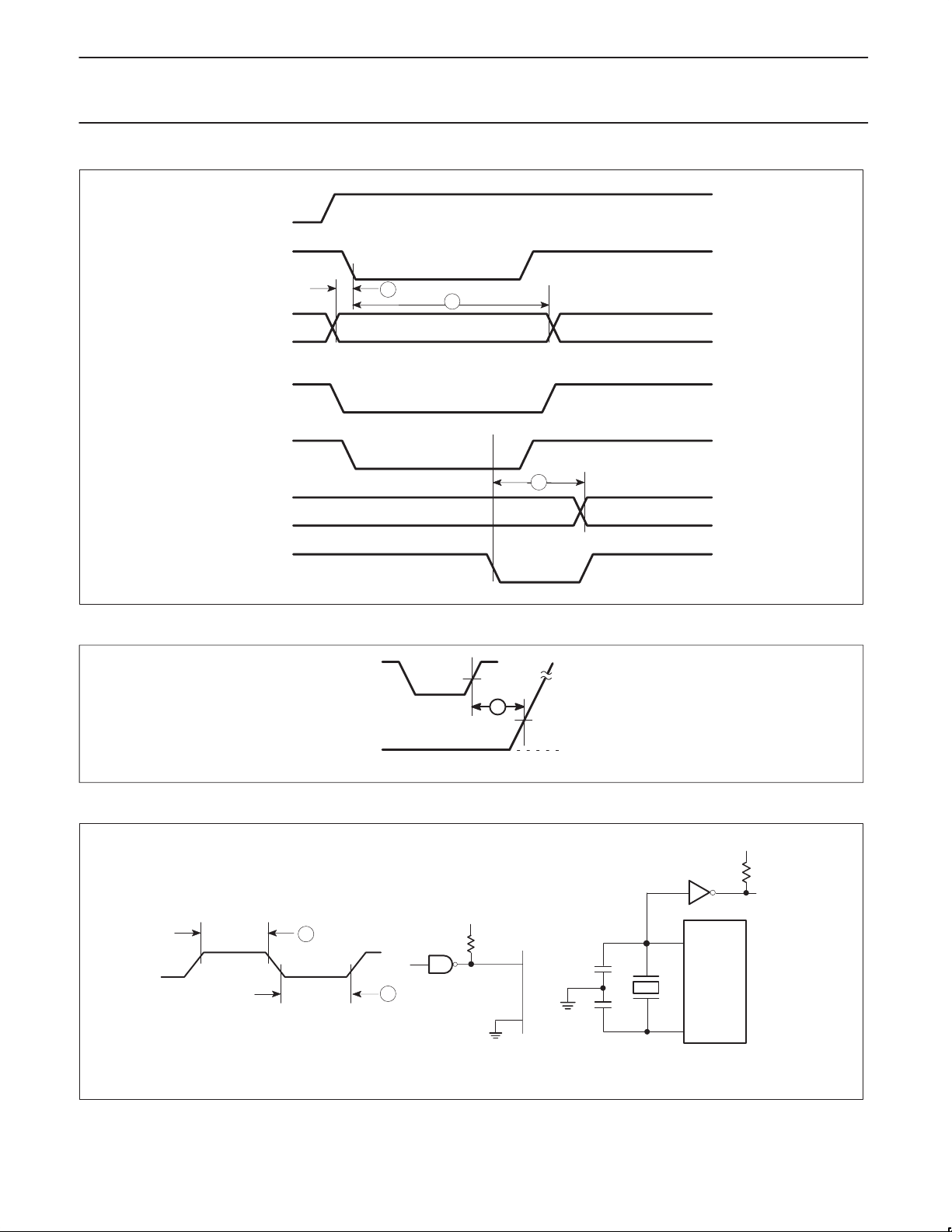
Figure 8. Port Timing
CSN
V
M
19
IRQN
V
+0.5V
OL
SD00231
V
OL
Figure 9. Interrupt Timing
+5V
C1 = C2: 0-5pF + (STRAY < 5pF)
DRIVING FROM
EXTERNAL
SOURCE
+5V
20
20
470Ω
X1
X2
C1
C2
14.7456 MHz
CRYSTAL SERIES RESISTANCE3 SHOULD
BE LESS THAN 180Ω
X1
DUSCC
X2
1K
CLOCK
TO OTHER
CHIPS
SD00232
Figure 10. Clock Timing
1995 May 01
11
Page 12
Philips Semiconductors Product specification
SCN68562Dual universal serial communications controller (DUSCC)
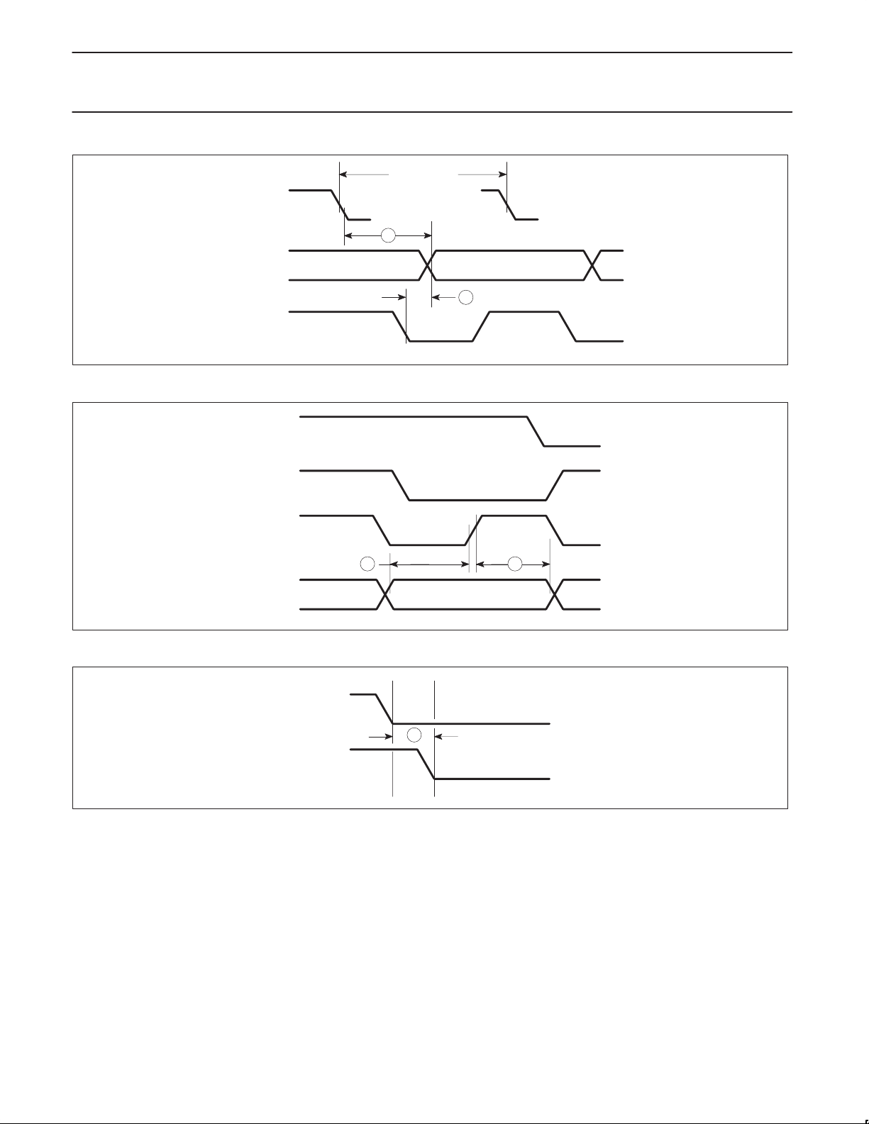
1 BIT TIME
(1 OR 16 CLOCKS)
TxC
(INPUT)
21
TxD
TxC
(1X OUTPUT)
SYNOUT
SYNIN
RxC (1x)
INPUT
22
SD00227
Figure 11. Transmit Timing
23 24
RxD
SD00233
Figure 12. Receive Timing
1995 May 01
IACKN
25
IDCN
SD00234
Figure 13. Interrupt Daisy Chain Timing
12
Page 13
Philips Semiconductors Product specification
SCN68562Dual universal serial communications controller (DUSCC)
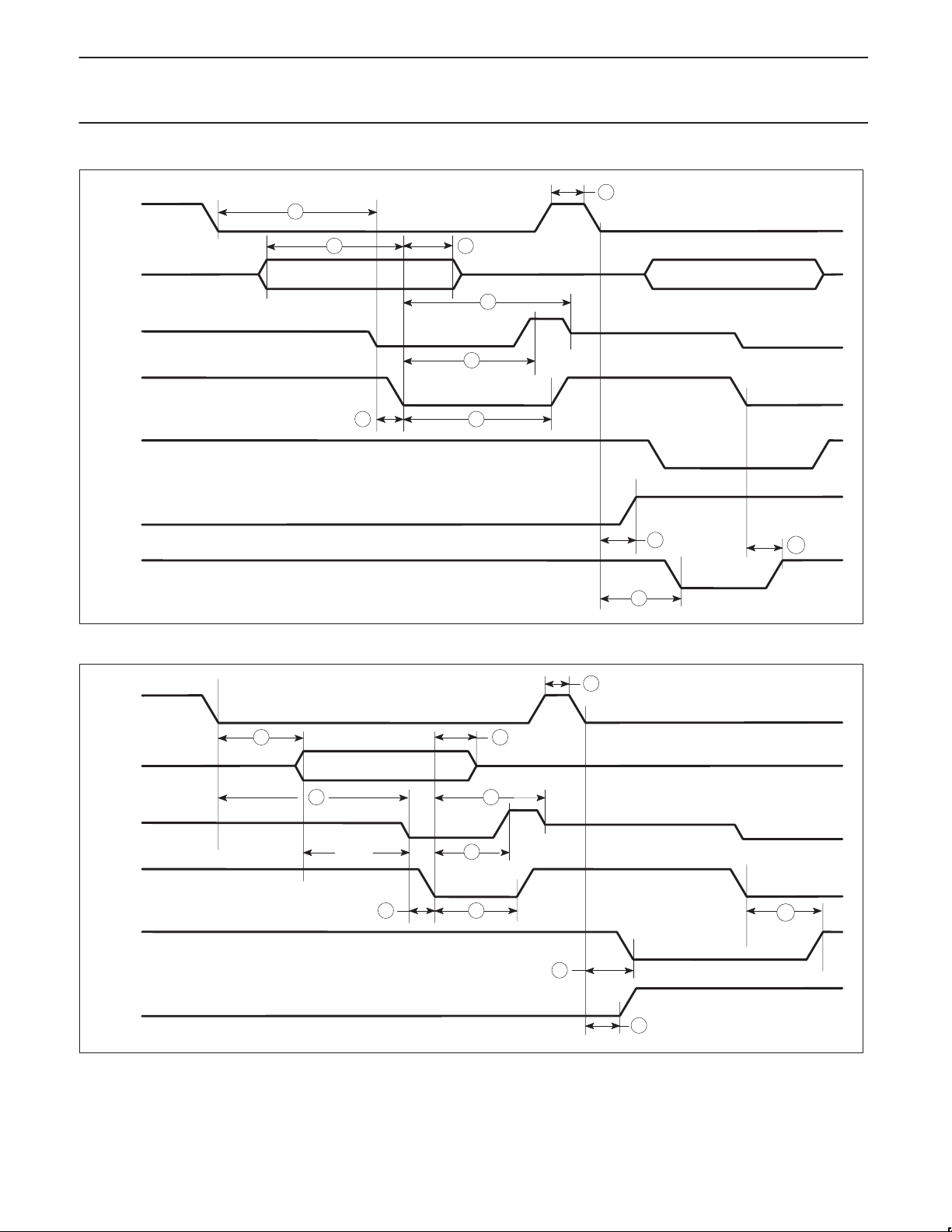
39
TxDAKN
D0–D7
RDYN
(DTACKN)
DTCN
DONEN
(INPUT)
30
36 37
32
31
28 27
TxDRQN
DONEN
(OUTPUT)
RTxDAKN
D0–D7
RDYN
(DTACKN)
DTCN
DONEN
(OUTPUT)
Figure 14. DMA Transmit W rite Timing—Single Address DMA Mode
34
26 29
30
28 27
32
31
35
38
40
40A
SD000235
40A
RTxDRQN
1995 May 01
33
SD00236
Figure 15. DMA Receive Read Timing—Single Address DMA Mode
13
Page 14
Philips Semiconductors Product specification
SCN68562Dual universal serial communications controller (DUSCC)
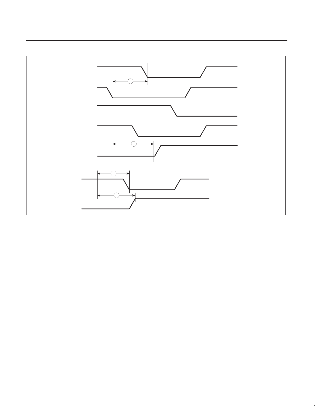
DONEN
(OUTPUT)
41
CSN
DTACKN
DONEN
(INPUT)
42
TxDRQN
DONEN (OUTPUT)
(EOM)
RTxDRQN
TRANSMIT DUAL ADDRESS DMA MODE
43
44
SD00237
Figure 16. Dual Address DMA Mode Timing
1995 May 01
14
Page 15
Philips Semiconductors Product specification
SCN68562Dual universal serial communications controller (DUSCC)
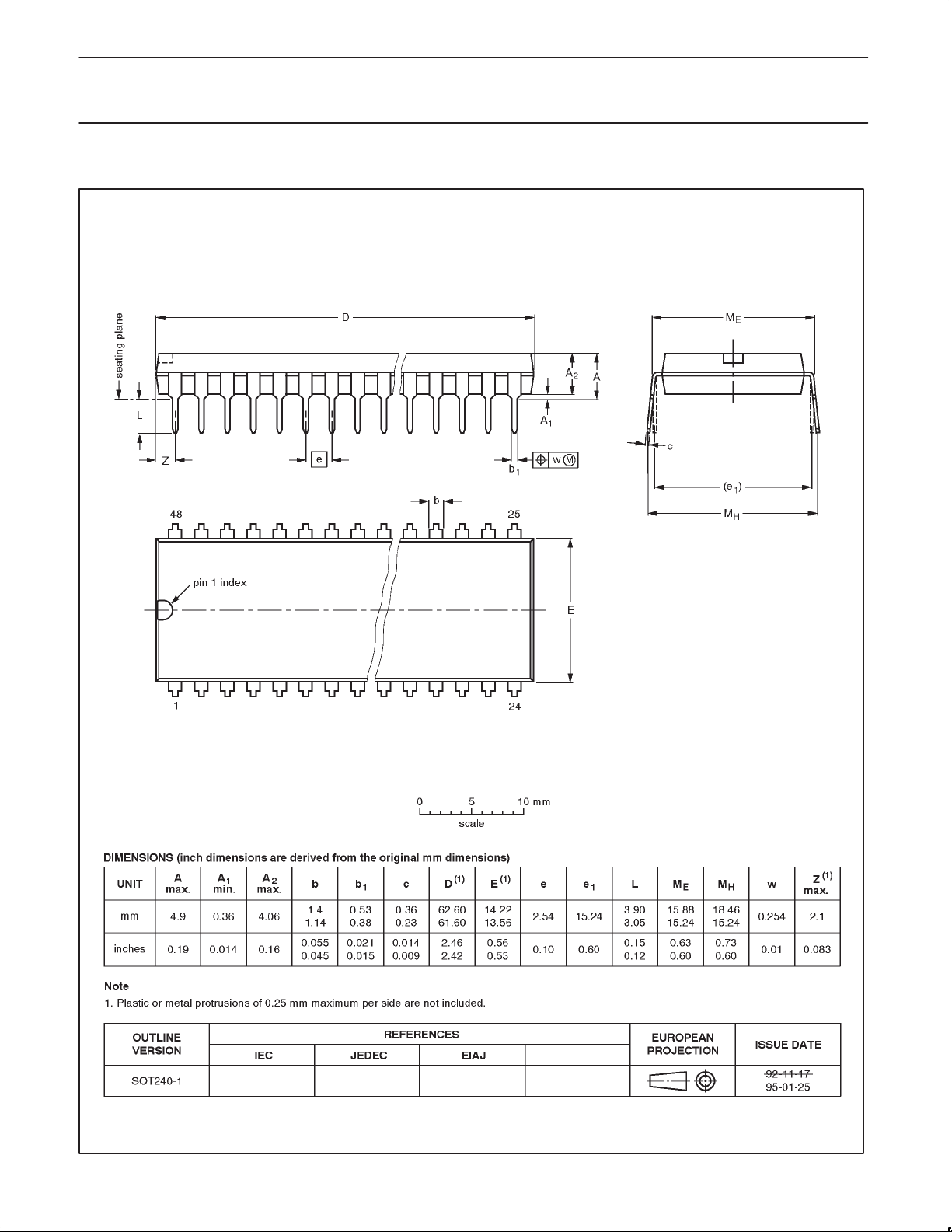
DIP48: plastic dual in-line package; 48 leads (600 mil) SOT240-1
1995 May 01
15
Page 16
Philips Semiconductors Product specification
SCN68562Dual universal serial communications controller (DUSCC)
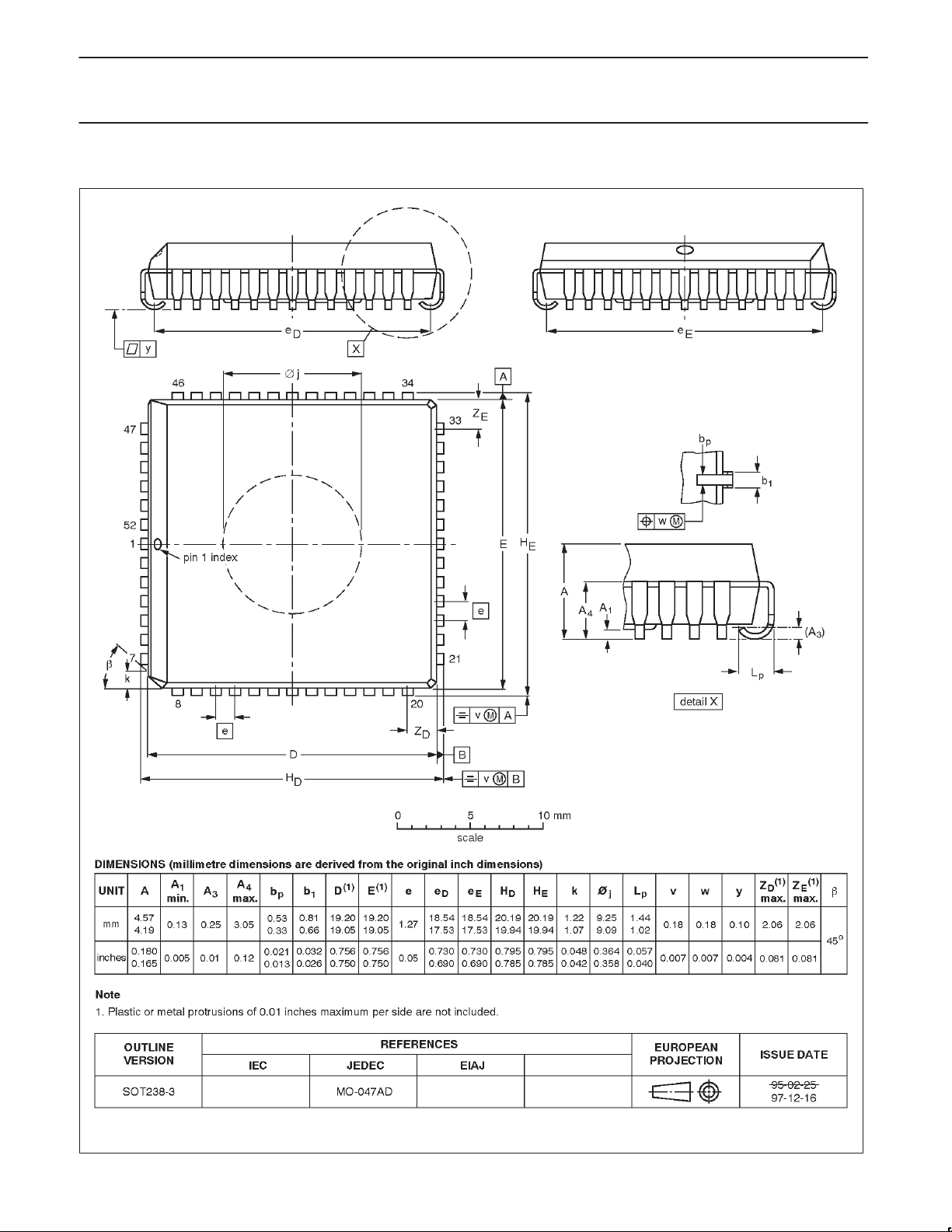
PLCC52: plastic leaded chip carrier; 52 leads; pedestal SOT238-3
1995 May 01
16
Page 17

Philips Semiconductors Product specification
SCN68562Dual universal serial communications controller (DUSCC)
NOTES
1995 May 01
17
Page 18

Philips Semiconductors Product specification
SCN68562Dual universal serial communications controller (DUSCC)
Data sheet status
Data sheet
status
Objective
specification
Preliminary
specification
Product
specification
Product
status
Development
Qualification
Production
Definition
This data sheet contains the design target or goal specifications for product development.
Specification may change in any manner without notice.
This data sheet contains preliminary data, and supplementary data will be published at a later date.
Philips Semiconductors reserves the right to make chages at any time without notice in order to
improve design and supply the best possible product.
This data sheet contains final specifications. Philips Semiconductors reserves the right to make
changes at any time without notice in order to improve design and supply the best possible product.
[1]
[1] Please consult the most recently issued datasheet before initiating or completing a design.
Definitions
Short-form specification — The data in a short-form specification is extracted from a full data sheet with the same type number and title. For
detailed information see the relevant data sheet or data handbook.
Limiting values definition — Limiting values given are in accordance with the Absolute Maximum Rating System (IEC 134). Stress above one
or more of the limiting values may cause permanent damage to the device. These are stress ratings only and operation of the device at these or
at any other conditions above those given in the Characteristics sections of the specification is not implied. Exposure to limiting values for extended
periods may affect device reliability.
Application information — Applications that are described herein for any of these products are for illustrative purposes only. Philips
Semiconductors make no representation or warranty that such applications will be suitable for the specified use without further testing or
modification.
Disclaimers
Life support — These products are not designed for use in life support appliances, devices or systems where malfunction of these products can
reasonably be expected to result in personal injury . Philips Semiconductors customers using or selling these products for use in such applications
do so at their own risk and agree to fully indemnify Philips Semiconductors for any damages resulting from such application.
Right to make changes — Philips Semiconductors reserves the right to make changes, without notice, in the products, including circuits, standard
cells, and/or software, described or contained herein in order to improve design and/or performance. Philips Semiconductors assumes no
responsibility or liability for the use of any of these products, conveys no license or title under any patent, copyright, or mask work right to these
products, and makes no representations or warranties that these products are free from patent, copyright, or mask work right infringement, unless
otherwise specified.
Philips Semiconductors
811 East Arques Avenue
P.O. Box 3409
Sunnyvale, California 94088–3409
Telephone 800-234-7381
Copyright Philips Electronics North America Corporation 2000
All rights reserved. Printed in U.S.A.
Date of release: 01-00
Document order number: 9397 750 06825
1995 May 01
18
 Loading...