

Page 1
Silan
Semiconductors
INFRARED REMOTE CONTROL
TRANSMITTER
DESCRIPTION
The SC7461 is a remote control transmitter utilizing CMOS
Technology specially designed for infrared applications. It is
capable of controlling 32 function keys and 3 double keys. SC7461 is
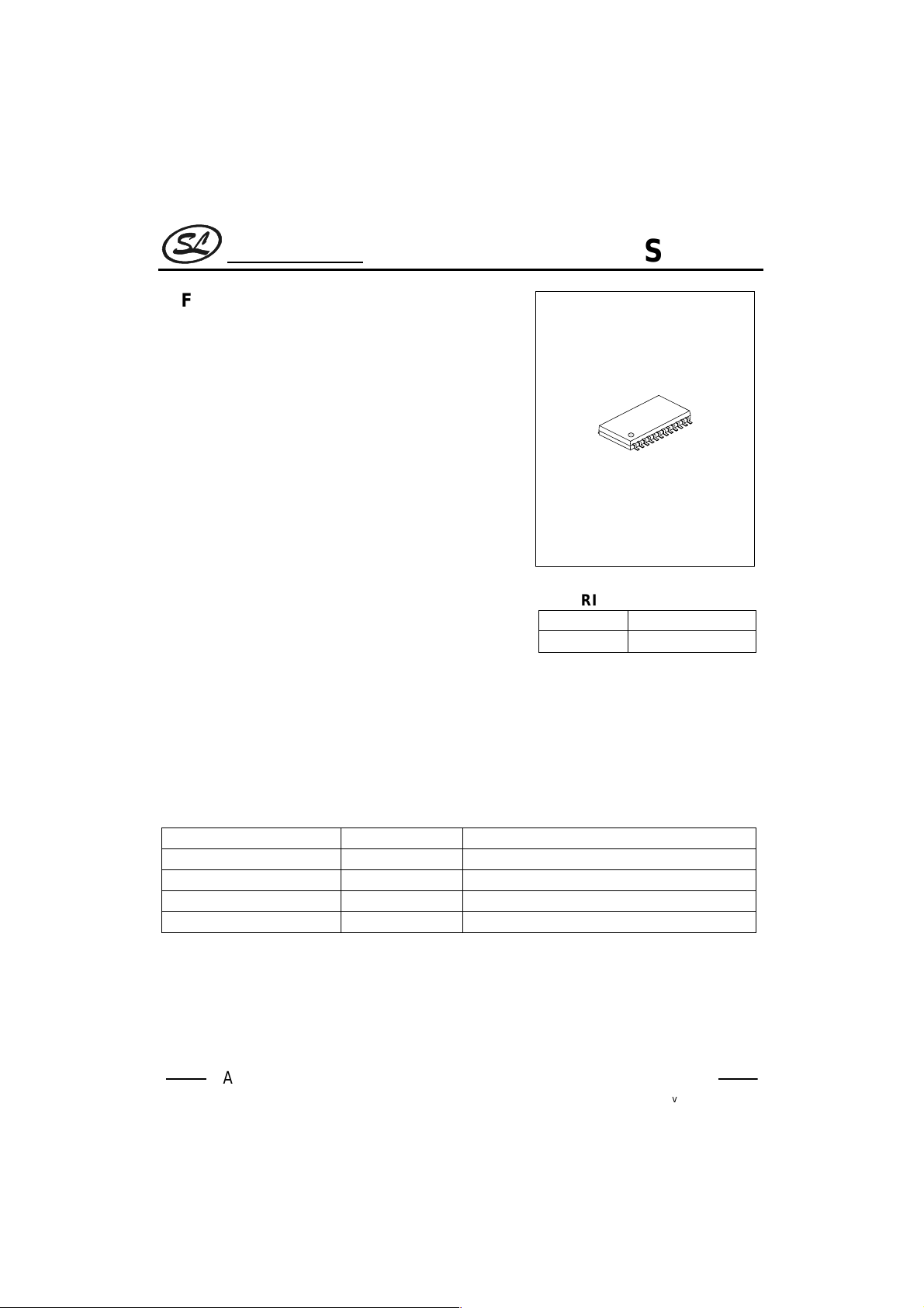
housed in 24 pins, SO Package and provides 13 bits Custom Code.
FEATURES
* CMOS Technology
* Low Power Consumption
* 32+3 Function Keys
* Least External Components
* Wide range of operating voltage: V
* Double key operation(No order of priority given)
* On-Chip Oscillator can be constructed using an externally
connected ceramic resonator
* Up to 64 Custom Codes may be selected externally for SC7461
APPLICATIONS
* TV and VCR
* Audio Equipment
ORDERING INFORMATION
Valid Part Number Package Custom Code in Mask ROM
SC7461-100 SOP-24 C6~C12=1000000
SC7461-101 SOP-24 C6~C12=0000000
SC7461-103 SOP-24 C6~C12=0010000
SC7461-104 SOP-24 C6~C12=1010000
HANGZHOU SILAN MICROELECTRONICS JOINT-STOCK CO.,LTD
=2.0~5.5V
DD
ORDERING INFORMATION
Part No. Package
SC7461 SOP-24-375-1.27
* Audio Cassette Deck
* Air Conditioner
* Multi-Media DVD Player
1
SC7461
SOP-24
Rev: 2.2 2002-02-28.
Page 2
Silan
Semiconductors
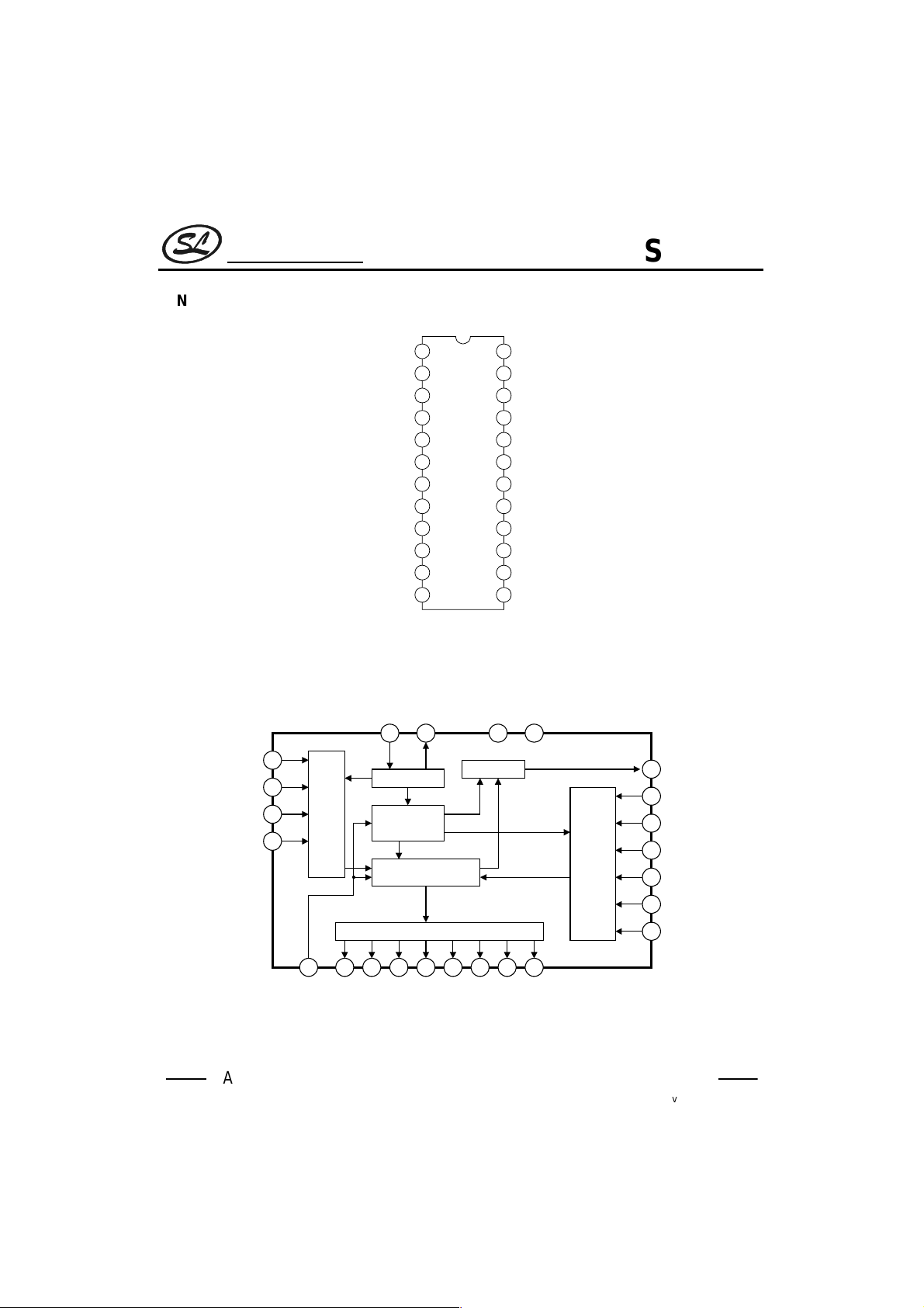
PIN CONFIGURATION
BLOCK DIAGRAM
KI0
1
KI1
2
KI2
KI3
3
4
Input
Scan
Circuit
KI0
KI1
KI2
KI3
C4
C5
OUT
V
DD
TEST
OSCI
OSCO
ss
V
OSCI OSCO V
OSC Circuit
Key
Timing
Generation
&Control Circuit
Code GenerationCircuit
Key OutputTiming SignalGenerator
1
2
3
4
5
6
SC7461
7
8
9
10
11
12
1110 8 12
Output Circuit
C3
24
C2
23
C1
22
C0
21
KO0
20
KO1
19
KO2
18
KO3
17
KO4
16
KO5
15
KO6
14
KO7
13
DDVSS
SC7461
OUT
7
C0
21
C1
22
Custom
Code
Register
23
24
C2
C3
C4
5
C5
6
1920 1718 1416 13149
TEST
KO0 KO1 KO2 KO3 KO4 KO5 KO6 KO7
HANGZHOU SILAN MICROELECTRONICS JOINT-STOCK CO.,LTD
Rev: 2.2 2002-02-28.
2
Page 3
Silan
Semiconductors
ABSOLUTE MAXIMUM RATING
Characteristic Symbol Description Value Unit
Maximum Supply Voltage V
Input Voltage V
Output Voltage V
Output Current I
Allowable Power Dissipation Pd
Storage Temperature T
Operating Temperature T
(Tamb=25°C, unless otherwise specified)
V
DD(max)
IN
OUT
OUT
(max)
stg
opr
DD
Each Input pin Vss-0.3~VDD+0.3 V
-- Vss-0.3~VDD+0.3 V
OUT -35 mA
Ta<=85°C
-- -40~+125
-- -10~+70
ELECTRICAL CHARACTERISTICS
Parameter Symbol Test conditions Min Typ Max Unit
Operating Supply Current I
Quiescent Supply Current I
High Level Output Current
High Level Output Voltage V
Low Level Output Voltage V
Output OFF-State Leakage Current I
Custom Code High Level Input Current I
Custom Code Low Level Input Current I
Input Floating Voltage V
Input Pull-Down Resistance R
(Tamb=25°C,VDD=3.0V,unless otherwise specified)
Key ON, Output: no load 1 mA
DD
All keys OFF, OSC stops 1
DS
I
OH1
I
OH2
OFF
OH
OL
IH
IL
VDD=1.8V, VOH=1.0V -8 mA
VDD=3.0V, VOH=2.0V -25 mA
IOH=1mA 2.4 V
IOL=1mA 0.2 V
-- 1
VIN=V
DD
VIN=V
SS
IF
IN
-- 0.1V
-- 75 100 125
-1
RECOMMENDED OPERATING CONDITIONS
(Tamb=25°C, fosc=455kHz,unless otherwise specified)
Characteristic Symbol Min. Typ. Max. Unit
Supply Voltage V
High Level Input Voltage V
Low Level Input Voltage V
Oscillation Frequency fosc 400 455 500 KHz
DD
IH
IL
2.0 3.0 3.3 V
0.7V
DD
Vss 0.3V
SC7461
Vss-0.3~10 V
150 mW
1
DD
V
DD
DD
°C
°C
V
V
µA
µA
µA
µA
V
kΩ
HANGZHOU SILAN MICROELECTRONICS JOINT-STOCK CO.,LTD
Rev: 2.2 2002-02-28.
3
Page 4
Silan
Semiconductors
PIN DESCRIPTION
Pin No. Symbol I/O Description
1~4 KI0~KI3 I Key Input Pins
7 OUT O Output Pins For Transit LED Drive
8VDD-- Power Supply
9 TEST I LSI Test Pin. This pin is normally set to High State or Floating.
10 OSCI I Oscillator Input Pin
11 OSCO O Oscillator Output Pin
12 V
13~20 KO7~KO0 O Key Scan Timing Signal Output Pins
21~24
5,6
SS
C0~C3
C4~C5
-- Power Supply Vss=GND
Custom Code Input Pins. Capable of externally setting 6 out of
I
13 bits for custom coding.
FUNCTIONAL DESCRIPTION
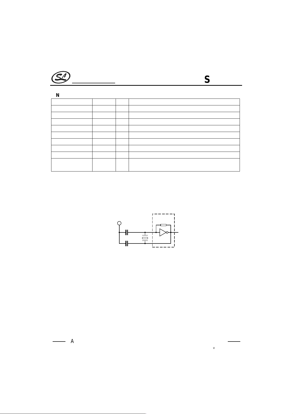
1.OSCILLATION CIRCUIT
A self-biased type amplifier is housed by a CMOS Inverter Method. Thus, an oscillation circuit can be
constructed by connecting a ceramic resonator. Please refer to Figure 4 for the oscillation circuit diagram.
SC7461
V
DD
100pF
455KHz
100pF
FIGURE 1. OSCILLATION CIRCUIT DIAGRAM
Unless the keys are being operated, the oscillation is normally stopped. Thus, power consumption is considerably
reduced.
2.KEY INPUT
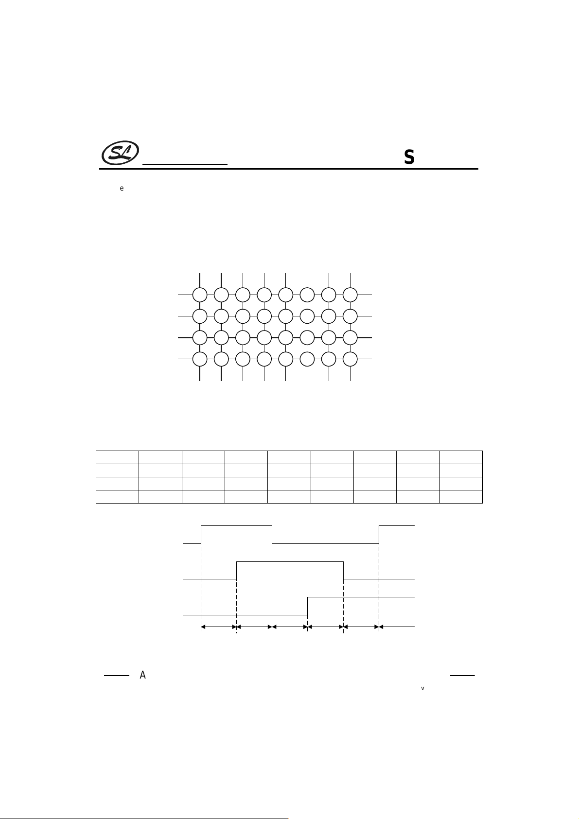
A total of 32 keys can be connected by Key Inputs--KI0~KI3 and Timing Signals--KO0~KO7. Double Key
Operation is possible for only Key No.20 in combination with the other keys connected to the KO5 line, namely: Key
No.21, 22 or 23. Thus, only the following key combinations may be used for the double key operation:
1).Key Nos.20 and 21
2).Key Nos.20 and 22
3).Key Nos.20 and 23
SC7461
HANGZHOU SILAN MICROELECTRONICS JOINT-STOCK CO.,LTD
Rev: 2.2 2002-02-28.
4
Page 5
Silan
Semiconductors
There is no order of priority given in key input. This means that keys designated for the double keying operation
may be pressed in any sequence. When two keys (designated for the double key operation) are pressed
simultaneously, a series of pulse is outputted according to each key input. Pressing other keys that are NOT
intended for the double key operation do NOT generate any output.
The Key Matrix is given in the following diagram.
KO0 KO1 KO2 KO3 KO4 KO5 KO6 KO7
SC7461
84 1612 24200 28
51 139 2117 2925
62 1410 2218 3026
73 1511 2319 3127
FIGURE 2. KEY MATRIX
3.DOUBLE KEY OPERATION
Double Key Operation is useful for tape deck recording operation. The following table shows the Key Data
corresponding to the double keys pressed. Also refer to the Key Input Section.
KI0
KI1
KI2
KI3
Key D0 D1 D2 D3 D4 D5 D6 D7
K20+K2110101100
K20+K2201101100
K20+K2311101100
NOTE: Key Data--D6 and D7 may be preset to "0", "1" by mask option.
Key 20
Key 21
(H=Key-ON)
Key 22
Key 20
Transmission
Key 20&21
Transmission
Data
FIGURE 3. TRANSMISSION DATA DI AGRAM
Data
Key 21
Transmission
Data
Transmission
Stops
Key 22
Transmission
Data
Key 20&22
Transmission
Data
HANGZHOU SILAN MICROELECTRONICS JOINT-STOCK CO.,LTD
Rev: 2.2 2002-02-28.
5
Page 6

Silan
Semiconductors
When any of the double key combinations (Key No.20&21, Key No.20&22 and Key No.20&23) are pressed:
1).D5 is set to "1"
2).No Key Input Sequence is needed to perform the Double Key Operation
4.SC7461 DATA FRAME
A SC7461 Data Frame consists of 42 bits, namely: 13 bits Custom Code (C0~C12), 8 bits Key Data (D0~D7),
and their respective Inverse Codes. Please refer to the figure below.
C0 C1 C2 C3 C5C4 C6 C8
Custom Code (13 bits) Custom Code (13bits) Key Data (8 bits) Key Data( 8 bits)
CUSTOM CODE
The Custom Code consists of 13 bits, namely: C0~C12. 7 bits--C6~C12-- are fixed by the on-chip ROM while 6
bits--C0~C5--are pin-settable. SC7461 provides up to 64 custom codes that may be selected externally without any
diode requirement. Please refer to the illustration below.
C9 C10 C11 C12
D0 D1 D2 D3 D4 D0 D1 D2 D3 D4 D5 D6 D7D5 D6 D7
C11C12C10C8C7C6C5C4C3C2C1C0
FIGURE 4. SC7461 DATA FRAME
SC7461
C0 C1 C2 C3 C5C4 C6 C8
Pin-Settable
6Bits
FIGURE 5. SC7461 CU STOM CODE
For example: Given the following setting,
C5
C4
C3
C2
SC7461
C1
C0
FIGURE 6. EXAMPLE CUSTOM CODE SETTING
then, the Custom Codes C0~C5 will have the following values:C0=0, C1=1, C2=1, C3=0, C4=0, C5=1.
Mask ROM
V-
6
5
24
23
22
21
C9 C10 C11C12
7Bits
HANGZHOU SILAN MICROELECTRONICS JOINT-STOCK CO.,LTD
6
Rev: 2.2 2002-02-28.
Page 7

Silan
Semiconductors
KEY DATA
The Key Data has 8 bits (D0~D7) and has the following Key Data Codes. D6 and D7 may be preset to "0", "1".
Key D0 D1 D2 D3 D4 D5 D6 D7
000000000
110000000
201000000
311000000
400100000
510100000
601100000
711100000
800010000
910010000
1001010000
1111010000
1200110000
1310110000
1401110000
1511110000
1600001000
1710001000
1801001000
1911001000
2000101000
2110101000
2201101000
2311101000
2400011000
2510011000
2601011000
2711011000
2800111000
2910111000
3001111000
3111111000
SC7461
HANGZHOU SILAN MICROELECTRONICS JOINT-STOCK CO.,LTD
Rev: 2.2 2002-02-28.
7
Page 8

Silan
Semiconductors
5.SC7461 TRANSMISSION CODE
The SC7461 transmission code consists of a leader code, 13 bits custom code, and 8 bits key data codes. The
inverse code of both the custom and key data codes are also sent simultaneously; thus, allowing an extremely low
error rate in the system configuration. Please refer to the following diagram.
SC7461
C0 C1 C2 C3 C5C4 C6 C8
Leader Code Custom Code (13 bits) Custom Code (13 bits) Key Data (8 bits) Key Data ( 8 bits)
The leader code consists of a 9ms carrier waveform followed by a 4.5ms OFF waveform. It is used as the leader
for the following codes (Custom, Data and their respective inverse codes). Thus, when the reception is configured by
a microcomputer, the time relationship between the reception detection and other processes can be managed
efficiently. The code uses the PPM (Pulse Position Modulation) Method, with "1" and "0" differentiated by the time
between pulses.
C9 C10 C11 C12
FIGURE 13. REM OUTPUT CODES
D0 D1 D2 D3 D4 D0 D1 D2 D3 D4 D5 D6 D7D5 D6 D7
C11C12C10C8C7C6C5C4C3C2C1C0
HANGZHOU SILAN MICROELECTRONICS JOINT-STOCK CO.,LTD
Rev: 2.2 2002-02-28.
8
Page 9

Silan
Semiconductors
6.SC7461 TRANSMISSION W AVEFORM
The SC7461 Transmission Waveform illustrated below were derived from the time period for fosc=455KHz.
84.4ms
108ms
9ms
4.5ms
13.5ms
Leader
Code
First Transmission
Custom Code
108ms
Go To Second
Transmission
13bits
43.9ms 27ms
84.4ms
Go To Second
Transmission and Onwards
Custom Code
13 bits
Key Data
8bits
SC7461
Key Data
8bits
1.125ms
0.56ms
0.56ms
1001
0 1 1
2.25ms
9ms 4.5ms
13.5ms
Second Transmission Onwards
9ms
13.5ms
4.5ms
(Transmission is available only when key input contimues)
Carrier Waveform
8.77µs
Carrier Frequency=1/12 fosc=38KHz
26.3µs
FIGURE 8. SC7461 TRANSMISSION WAVEFORM
HANGZHOU SILAN MICROELECTRONICS JOINT-STOCK CO.,LTD
Rev: 2.2 2002-02-28.
9
Page 10

Silan
Semiconductors
TYPICAL APPLICATION CIRCUITS
Note:1. Two capacitance connect with V
2. The line between two capacitance and V
KI3
4
KI2
3
KI1
2
KI0
1
V
DD
455KHz
11 10 689
KO7 OSCO
FIGURE 9. SC7461 APPLI CATION CIRCUI T DIAGRAM
100pF100pF
OSCI
TEST
SC7461
KO5
KO6
V
DD
DD
C5
V
KO4
V
DD
V
DD
2223245 21
C4
C3
C2
C1
C0
270
¡
7
OUT
1
Vss
KO0
KO1
KO2
KO3
DD should as near as possible.
19181716151413 20
DD and ground should as short as possible.
¡
12
C0=0
C1=1
C2=0
C3=1
C4=0
C5=1
SC7461
IR
LED
V
DD
0.1F47F
CHIP TOPOGRAPHY
21
22
23
24
1
HANGZHOU SILAN MICROELECTRONICS JOINT-STOCK CO.,LTD
20 19 18 17 16 15
Size: 1.84 x 1.46 mm
10
2
14
13
12
11
10
8765432
9
Rev: 2.2 2002-02-28.
Page 11

Silan
Semiconductors
PAD COORDINATES
No. Symbol X Y No. Symbol X Y
1 P1 -717.3 -273.5 13 P13 721.6 291.1
2 P2 -762.3 -532.3 14 P14 721.6 475.3
3 P3 -592.3 -532.3 15 P15 444.0 532.2
4 P4 -416.9 -532.3 16 P16 274.0 532.2
5 P5 -246.9 -532.3 17 P17 89.8 532.2
6 P6 -76.9 -532.3 18 P18 -80.2 532.2
7 P7 98.1 -532.3 19 P19 -264.4 532.2
8 P8 496.6 -532.3 20 P20 -434.4 532.2
9 P9 721.6 -569.3 21 P21 -717.3 407.0
10 P10 721.6 -399.3 22 P22 -717.3 237.0
11 P11 721.6 -223.9 23 P23 -717.3 67.0
12 P12 721.6 -53.9 24 P24 717.3 -103.0
Note: The original point of the coordinate is the die center.
(Unit: µm)
SC7461
HANGZHOU SILAN MICROELECTRONICS JOINT-STOCK CO.,LTD
Rev: 2.2 2002-02-28.
11
Page 12

Silan
Semiconductors
PCB WIRE LAYOUT SCHEMATIC:
SC7461
Transmitting tube output ground line
The transmitting tube ground line and IC ground line should
layout separated or overstriking ground line.
The above IC only use to hint, not to specified.
Note:
* In wire layout, the power filter capacitor should near to IC.
* In wire layout, should avoid power line and ground line too long.
* Recommended infrared transmit unit and IC ground line should layout separated, or overstriking lines.
* The emitter of triode connect 1
* Recommended triode use 9014.
resistor at least.
HANGZHOU SILAN MICROELECTRONICS JOINT-STOCK CO.,LTD
12
Rev: 2.2 2002-02-28.
Page 13

Silan
Semiconductors
PACKAGE OUTLINE
SOP-24-375-1.27 Unit: mm
1.27
15.34B0.25
13.97
0.40B0.1
HANGZHOU SILAN MICROELECTRONICS JOINT-STOCK CO.,LTD
13
SC7461
0.3
0.4
B
B
7.6
10.2
9.525(375)
0.25B0.05
3.10MAX
Rev: 2.2 2002-02-28.
Page 14

Silan
Attach
Semiconductors
SC7461
Revision History
Data REV Description Page
2000.12.31 2.0 Change name of company in page footer
2001.12.12 2.1
Add the “Ordering information”
Modify the “Features “
Modify the “Absolute maximum rating” and “Recommended operating
2002.02.28 2.2
conditions”
Modify the “Figure 6. example custom code setting”
Modify “Typical application circuit”
Add the “PCB wire layout schematic”
Modify the “Package outline”
1
1
3
6
10
12
13
HANGZHOU SILAN MICROELECTRONICS JOINT-STOCK CO.,LTD
Rev: 2.2 2002-02-28.
14
 Loading...