

Page 1
Silan
Semiconductors
RADIO DATA SYSTEM (RDS)
DEMODULATOR
DESCRIPTION
The integrated CMOS circuit SC6579 is an RDS demodulator. It
recovers the additional inaudible RDS information which is
transmitted by FM radio broadcasting.
The data signal RDDA and the clock signal RDCL are provided
as outputs for further processing by a suitable decoder
(microcomputer).
FEATURES
• Anti-aliasing filter (2nd order)
• Integrated 57 kHz band-pass filter (8th order)
• Reconstruction filter (2nd order)
• Clocked comparator with automatic offset compensation
• 57 kHz carrier regeneration
• Synchronous demodulator for 57 kHz modulated RDS signals
• Selectable 4.332/8.664 MHz crystal oscillator with variable
dividers
• Clock regeneration with lock on bi-phase data rate
• Bi-phase symbol decoder with integrate and dump functions
• Differential decoder
• Signal quality detector
• Subcarrier output.
SC6579
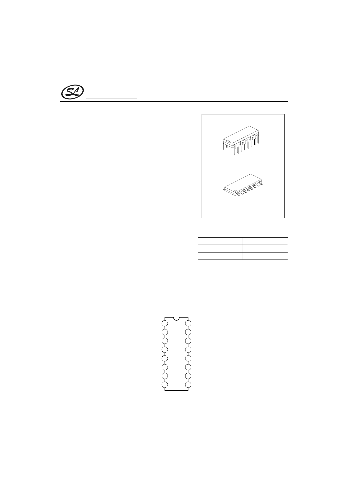
DIP-16
SOP-16
ORDERING INFORMATION
Device Package
SC6579 DIP16-300-2.54
SC6579S SOP-16-225-1.27
PIN CONFIGURATION
HANGZHOU SILAN MICROELECTRONICS JOINT-STOCK CO.,LTD
QUAL
RDDA
V
MUX
DDA
V
V
SSA
CIN
SCOUT
1
2
3
ref
4
5
6
7
8
SC6579
16
15
14
13
12
11
10
9
RDCL
T57
OSCO
OSCI
DDD
V
V
SSD
TEST
MODE
1
Rev: 1.0 2001.12.30
Page 2
Silan
Semiconductors
BLOCK DIAGRAM
SC6579
82pF
+5V
0.1F
DDD
V
121413
quality bit
generator
differential
decoder
SSD
MPX
signal
2.2
SCOUT
560pF
+5V V
0.1F
F
MUX
330pF
CIN
DDA
Vref
4
8
7
5
3
anti-
aliasing
filter
clocked
comparator
reference
voltage
6
47pF
4.332/8.664MHz
57kHz
bandpass
(8th order)
costas loop
variable and
fixed divider
P1
V
clock
regeneration
and sync
V
SSA
reconstruction
filter
SC6579
oscillator and
bi-phase
symbol
decoder
test logic and output
selector switch
91011
MODE TEST V
2.2K
OSCI OSCO
divider
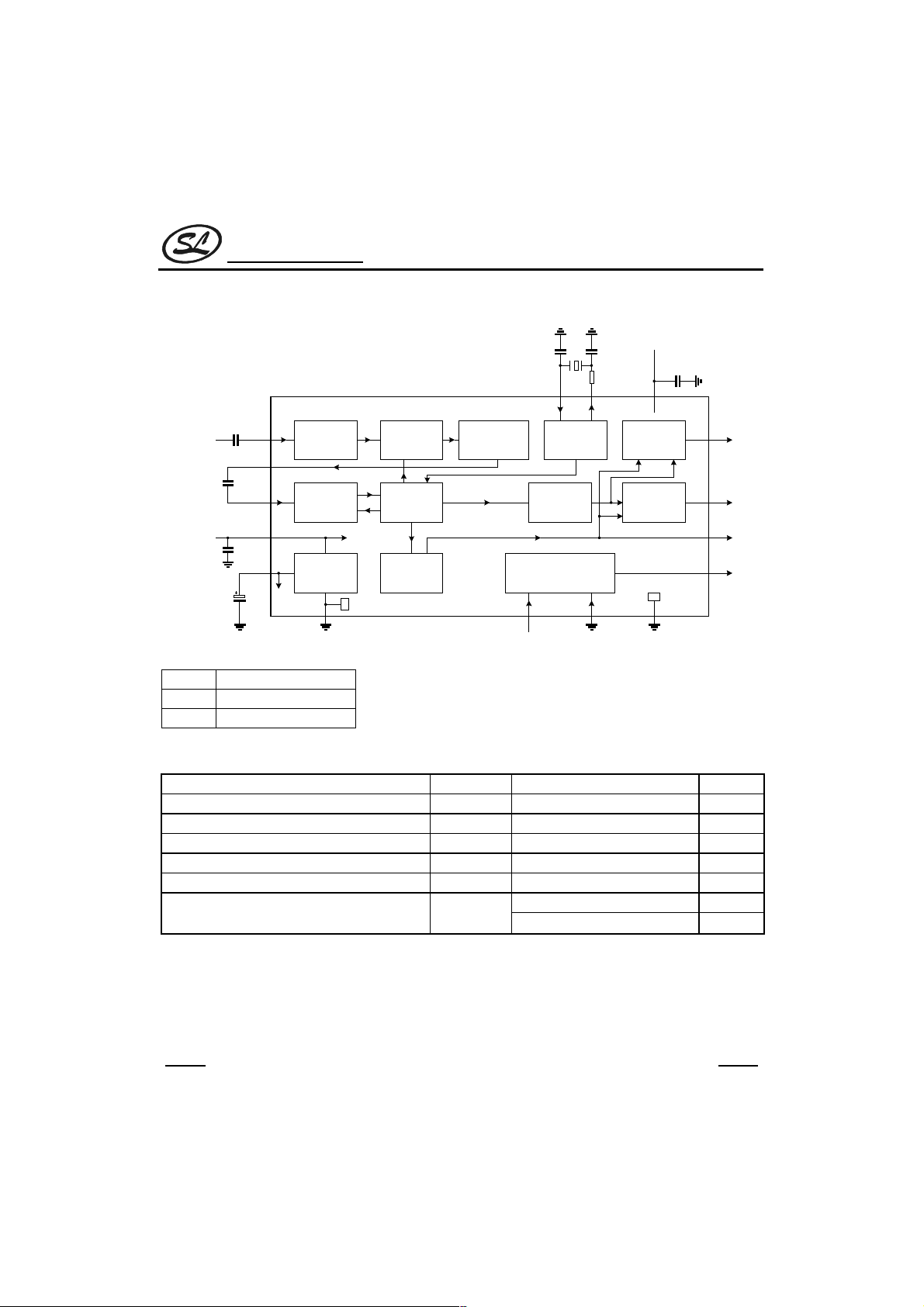
Via pin MODE two different crystal frequencies can be used.
MODE CRYSTAL CLOCK
LOW 4.332 MHz
HIGH 8.664 MHz
ABSOLUTE MAXIMUM RATINGS
Characteristic Symbol Value Unit
Analog Supply Voltage (pin 5) V
Digital Supply Voltage (pin 12) V
Voltage on All Pins; Grounds Excluded Vn -0.5 ~ V
Storage Temperature T
Operating Ambient Temperature T
Electrostatic Handling for All Pins Except
Pins 9 and 10
Notes1. Equivalent to discharging a 200 pF capacitor via a 0 Ω series resistor.
2. Equivalent to discharging a 100 pF capacitor via a 1.5 kΩ series resistor.
(Ta=25°C)
0~ 6 V
DDA
0~ 6 V
DDD
+ 0.5 V
DD
-40 ~+150 °C
stg
-40 ~+85 °C
amb
V
ESD
±300 note 1 V
+1500 ~-3000 note 2 V
QUAL
1
RDDA
2
RDCL
16
15 T57
HANGZHOU SILAN MICROELECTRONICS JOINT-STOCK CO.,LTD
2
Rev: 1.0 2001.12.30
Page 3
Silan
Semiconductors
ELECTRICAL CHARACTERISTICS
(V
=V
DDD
=5 V; T
DDA
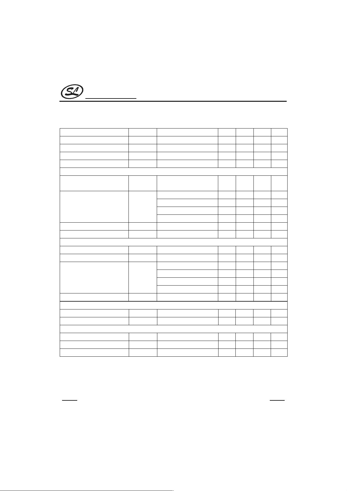
Parameter Symbol Test condition Min. Typ. Max. Unit
Analog Supply Voltage (pin 5) V
Digital Supply Voltage (pin 12) V
Total Supply Current I
Reference Voltage (pin 3) V
MPX input (signal before the capacitor on pin 4)
RDS Amplitude (RMS value) V
Maximum Input Signal Capability
(peak-to-peak value)
Input Resistance R4-6 f = 0 to 100kHz 40 -- -Signal Gain G8-4 f = 57 kHz 17 20 23 dB
57 kHz band-pass filter
Center Frequency fc T
-3 dB Bandwidth B 2.5 3.0 3.5 kHz
Stop Band Gain G
Output Resistance (pin 8) R
Comparator input (pin 7)
Minimum Input Level (RMS value) V
Input Resistance Ri 70 110 150
Oscillator input (pin 13)
HIGH-level Input Voltage VIH V
LOW-level Input Voltage VIL V
Input Current II V
=25°C and measurements taken in Fig.1; unless otherwise specified.)
amb
3.6 5.0 5.5 V
DDA
3.6 5.0 5.5 V
DDD
tot
ref
i MPX (rms)
V
i MPX (p-p)
o(8)
i(rms)
I
V
+I12 6 mA
5
= 5 V 2.5 V
DDA
∆f ±1.2 kHz RDS;
∆f ±3.5 kHz ARI; see Fig.5
f = 5±2 kHz 200 -- -- mV
f < 50 kHz 1.4 -- -- V
f < 15 kHz 2.8 -- -- V
f > 70 kHz 3.5 -- -- V
= -40 to +85 °C 56.5 57.0 57.5 kHz
amb
∆f =±7 kHz
f < 45 kHz 40 -- -- dB
f < 20 kHz 50 -- -- dB
f > 70 kHz 40 -- -- dB
f = 57 kHz -- 26 --
f = 57 kHz -- 1 10 mV
= 5.0 V 4.0 -- -- V
DDD
= 5.0 V -- -- 1.0 V
DDD
= 5.5 V -- -- ±
DDD
31 -- -- dB
SC6579
1 -- -- mV
kΩ
Ω
kΩ
µA
To be continued
HANGZHOU SILAN MICROELECTRONICS JOINT-STOCK CO.,LTD
3
Rev: 1.0 2001.12.30
Page 4
Silan
Semiconductors
(Continued)
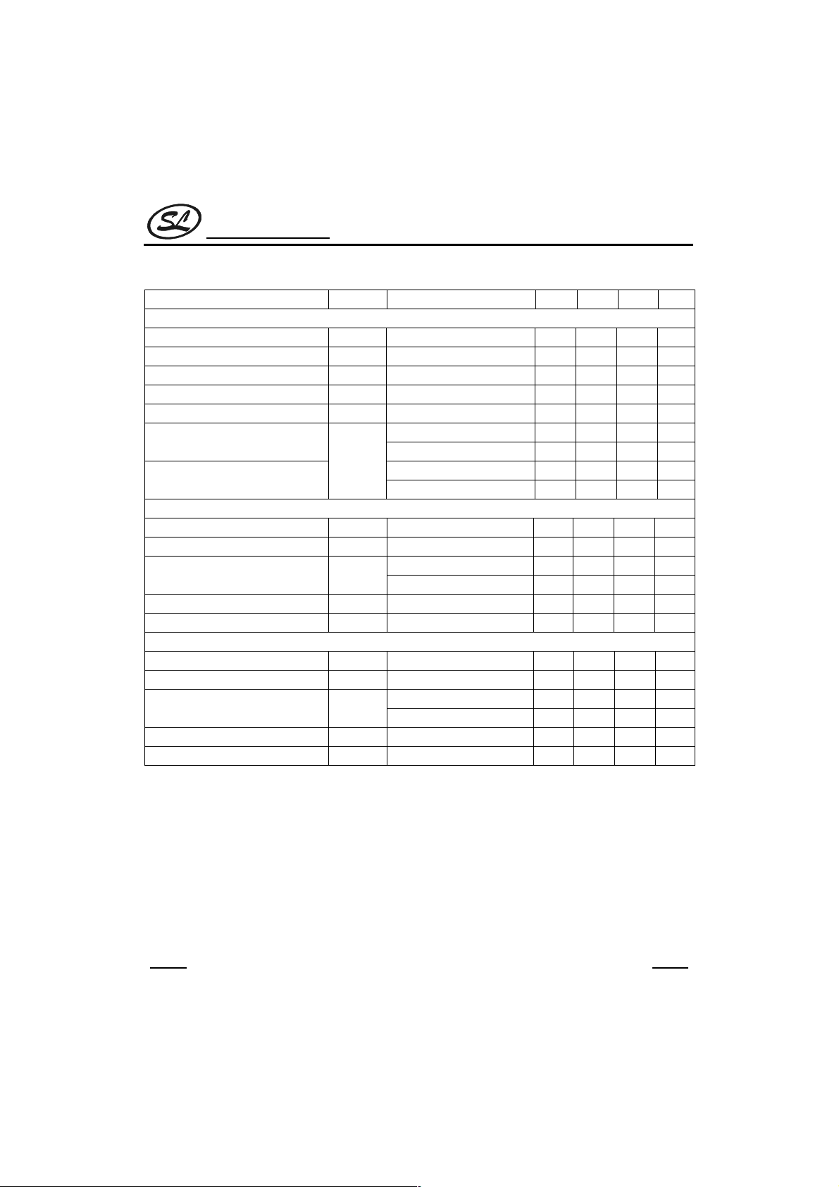
Parameter Symbol Test condition Min. Typ. Max. Unit
Digital demodulator and outputs QUAL, RDDA, T57, OSCO and RDCL (pins 1, 2, 14, 15 and 16)
HIGH-level output voltage VOH IQ = -20 mA; V
LOW-level output voltage VOL IQ = 3.2 mA; V
Nominal Clock Frequency RDCL f
Jitter of RDCL
Nominal Subcarrier Frequency T57 f
Output Current OSCO (pin 14)
RDCL (pins 1, 2, 15 and 16)
-- 1187.5 -- Hz
RDCL
∆
tRDCL
T57
I
-- -- 18
note 1 -- 57.0 -- kHz
V
= 4.5 V; V14 = 0.4 V 1.5 -- -- mA
DDD
V
= 4.5 V; V
DDD
O
V
= 4.5 V; VO = 0.4 V 5.9 -- -- mA Output Current QUAL, RDDA, T57,
DDD
V
= 4.5 V; VO = 4.1 V -5.3 -- -- mA
DDD
4.332 MHz crystal parameters
XTAL Frequency f0 -- 4.332 -- MHz
∆f
Maximum Permitted Tolerance
Adjustment Tolerance of f0
max
∆f
±50 10
T
=25°C -- -- ±20 10
amb
o
= -40 to +85 °C -- -- ±25 10
T
amb
Load Capacitance CL -- 30 -- pF
Resonance Resistance R
-- -- 60
xtal
8.664 MHz crystal parameters
XTAL Frequency f0 -- 8.664 -- MHz
∆f
Maximum Permitted Tolerance
Adjustment Tolerance of f0
max
∆f
-- ±50 -- 10
T
=25°C -- -- ±30 10
amb
o
T
= -40 to +85 °C -- -- ±30 10
amb
Load Capacitance CL -- 30 -- pF
Resonance Resistance R
-- -- 60
xtal
Note1. The signal T57 has a phase lead of 123° (±180°) relative to the ARI carrier at output SCOUT.
= 4.5 V 4.4 -- -- V
DDD
= 5.5 V -- -- 0.4 V
DDD
= 4.1 V -1.6 -- -- mA
14
SC6579
µs
-6
-6
-6
Ω
-6
-6
-6
Ω
HANGZHOU SILAN MICROELECTRONICS JOINT-STOCK CO.,LTD
4
Rev: 1.0 2001.12.30
Page 5
Silan
Semiconductors
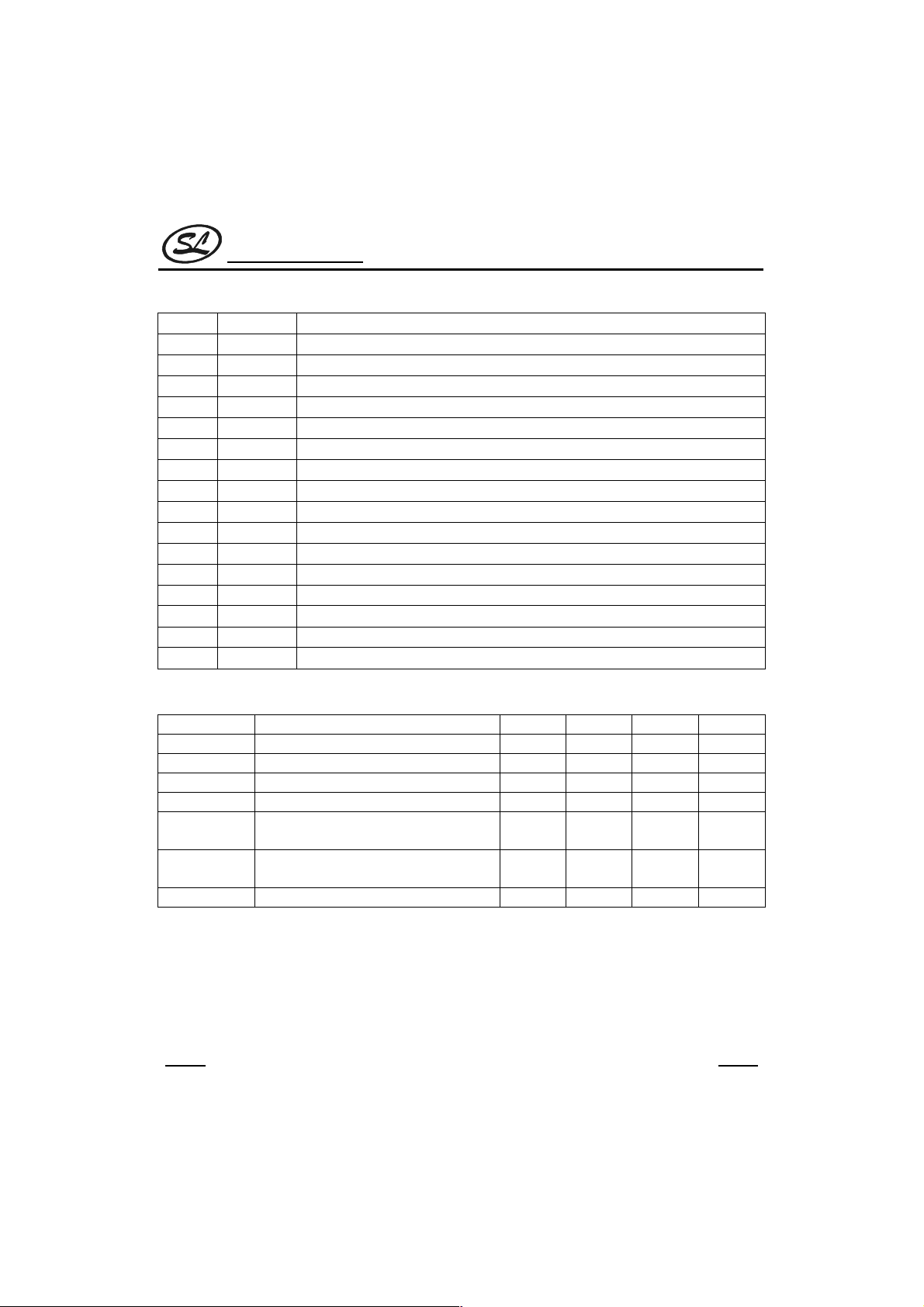
PIN DESCRIPTION
Pin no. Symbol Function
1 QUAL Quality indication output
2 RDDA RDS data output
3 Vref Reference voltage output (0.5 VDDA )
4 MUX Multiplex signal input
5 VDDA +5 V supply voltage for analog part
6 VSSA Ground for analog part (0V)
7 CIN Subcarrier input to comparator
8 SCOUT Subcarrier output of reconstruction filter
9 MODE Oscillator mode/test control input
10 TEST Test enable input
11 VSSD Ground for digital part (0V)
12 VDDD +5 V supply voltage for digital part
13 OSCI Oscillator input
14 OSCO Oscillator output
15 T57 57 kHz clock signal output
16 RDCL RDS clock output
QUICK REFERENCE DATA
SYMBOL PARAMETER MIN. TYP. MAX. UNIT
VDDA Analog Supply Voltage (pin 5) 3.6 5.0 5.5 V
VDDD Digital Supply Voltage (pin 12) 3.6 5.0 5.5 V
Itot Total Supply Current -- 6 -- mA
Vi(rms) RDS Input Amplitude (RMS value; pin 4) 1 -- -- mV
VOH HIGH-level Output Voltage for Signals
RDDA, RDCL, QUAL and T57
VOL LOW-level Output Voltage for Signals
RDDA, RDCL, QUAL and T57
Tamb Operating Ambient Temperature -40
4.4 -- -- V
-- -- 0.4 V
--
FUNCTION DESCRIPTION
The SC6579 is a demodulator circuit for RDS applications. It contains a 57 kHz bandpass filter and a digital
demodulator to regenerate the RDS data stream out of the multiplex signal (MPX).
SC6579
+85 °C
HANGZHOU SILAN MICROELECTRONICS JOINT-STOCK CO.,LTD
5
Rev: 1.0 2001.12.30
Page 6

Silan
Semiconductors
Filter part
The MUX signal is band-limited by a second-order anti-aliasing-filter and fed through a 57 kHz band-pass filter (8th
order band-pass filter with 3 kHz bandwidth) to separate the RDS signals. This filter uses switched capacitor
technique and is clocked by a clock frequency of 541.5 kHz derived from the 4.332/8.664 MHz crystal oscillator.
Then the signal is fed to the reconstruction filter to smooth the sampled and filtered RDS signal before it is output on
pin 8. The signal is AC-coupled to the comparator (pin 7). The comparator is clocked with a frequency of 228 kHz
(synchronized by the 57 kHz of the demodulator).
Digital part
The synchronous demodulator (Costa’s loop circuit) with carrier regeneration demodulates the internal coupled,
digitized signal. The suppressed carrier is recovered from the two sidebands (Costa’s loop). The demodulated signal
is low-pass-filtered in such a way that the overall pulse shape (transmitter and receiver) approaches a cosinusoidal
form in conjunction with the following Integrate and dump circuit.
The data-spectrum shaping is split into two equal parts and handled in the transmitter and in the receiver. Ideally,
the data filtering should be equal in both of these parts. The overall data-channel-spectrum shaping of the
transmitter and the receiver is approximately 100% roll-off. The integrate and dump circuit performs an integration
over a clock period. This results in a demodulated and valid RDS signal in form of bi-phase symbols being output
from the integrate and dump circuit. The final stages of RDS data processing are the bi-phase symbol decoding and
the differential decoding. After synchronization by data clock RDCL (pin 16) data appears on the RDDA output (pin
2). The output of the bi-phase symbol decoder is evaluated by a special circuit to provide an indication of good data
(QUAL = HIGH) or corrupt data (QUAL = LOW).
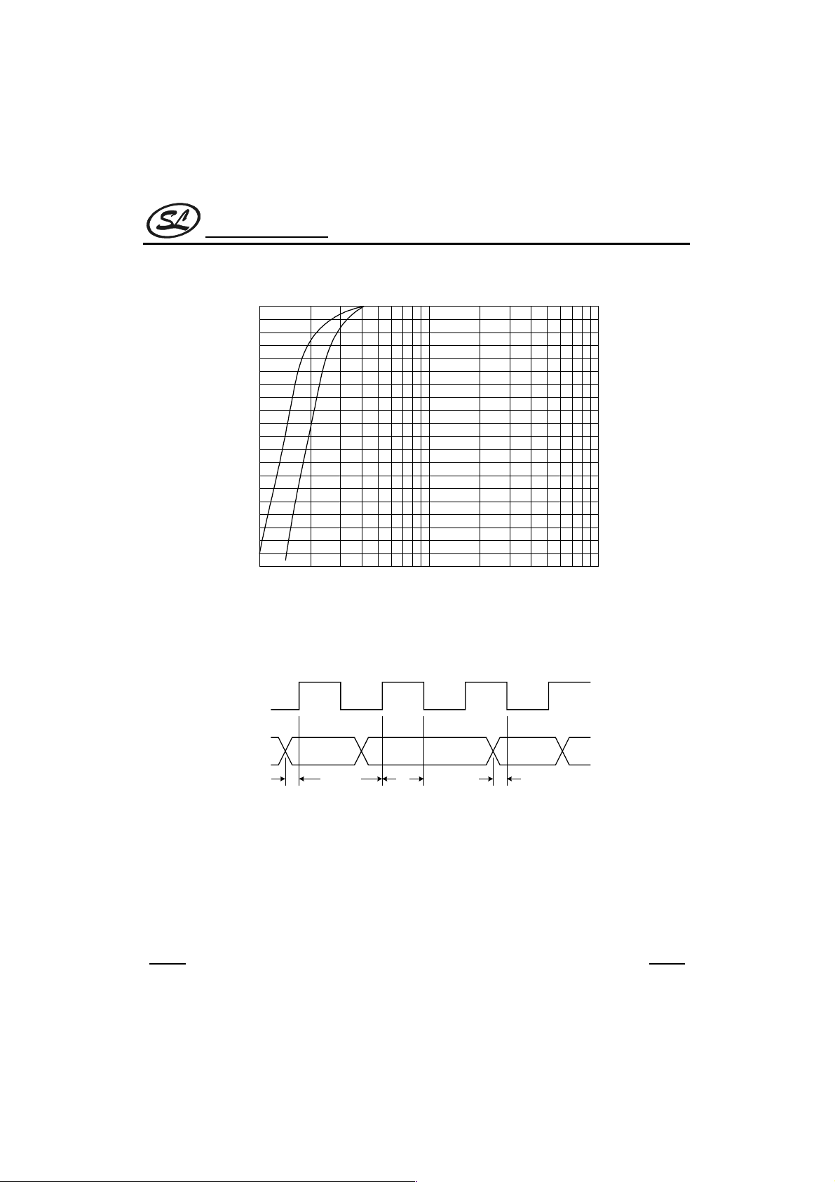
Timing
Fixed and variable dividers are applied to the 4.332/8.664 MHz crystal oscillator to generate the 1.1875 kHz RDS
clock RDCL, which is synchronized by the incoming data. Which ever clock edge is considered (positive or negative
going edge) the data will remain valid for 399 µs after the clock transition. The timing of data change is 4 µs before a
clock change. Which clock transition (positive or negative going clock) the data change occurs in, depends on the
lock conditions and is arbitrary (bit slip).
During poor reception it is possible that faults in phase occur, then the clock signal stays uninterrupted, and data is
constant for 1.5 clock periods. Normally, faults in phase do not occur on a cyclic basis. If however, faults in phase
occur in this way, the minimum spacing between two possible faults in phase depends on the data being transmitted.
The minimum spacing cannot be less than 16 clock periods. The quality bit changes only at the time of a data
change.
SC6579
HANGZHOU SILAN MICROELECTRONICS JOINT-STOCK CO.,LTD
6
Rev: 1.0 2001.12.30
Page 7
Silan
Semiconductors
TYPICAL RDS SENSITIVITY (BLOCK)
100
correct
blocks
(%)
75
SC6579
50
25
0
10
(1) RDS + ARI (BK)
(2) RDS only
TIMING DIAGRAM
RDCL
RDDA,
QUAL
(1)
-1
(2)
110
Vi(RDS signal, RMS value)
(mV)
842
s
4
s
421
s
4
s
MEH163
HANGZHOU SILAN MICROELECTRONICS JOINT-STOCK CO.,LTD
7
Rev: 1.0 2001.12.30
Page 8
Silan
Semiconductors
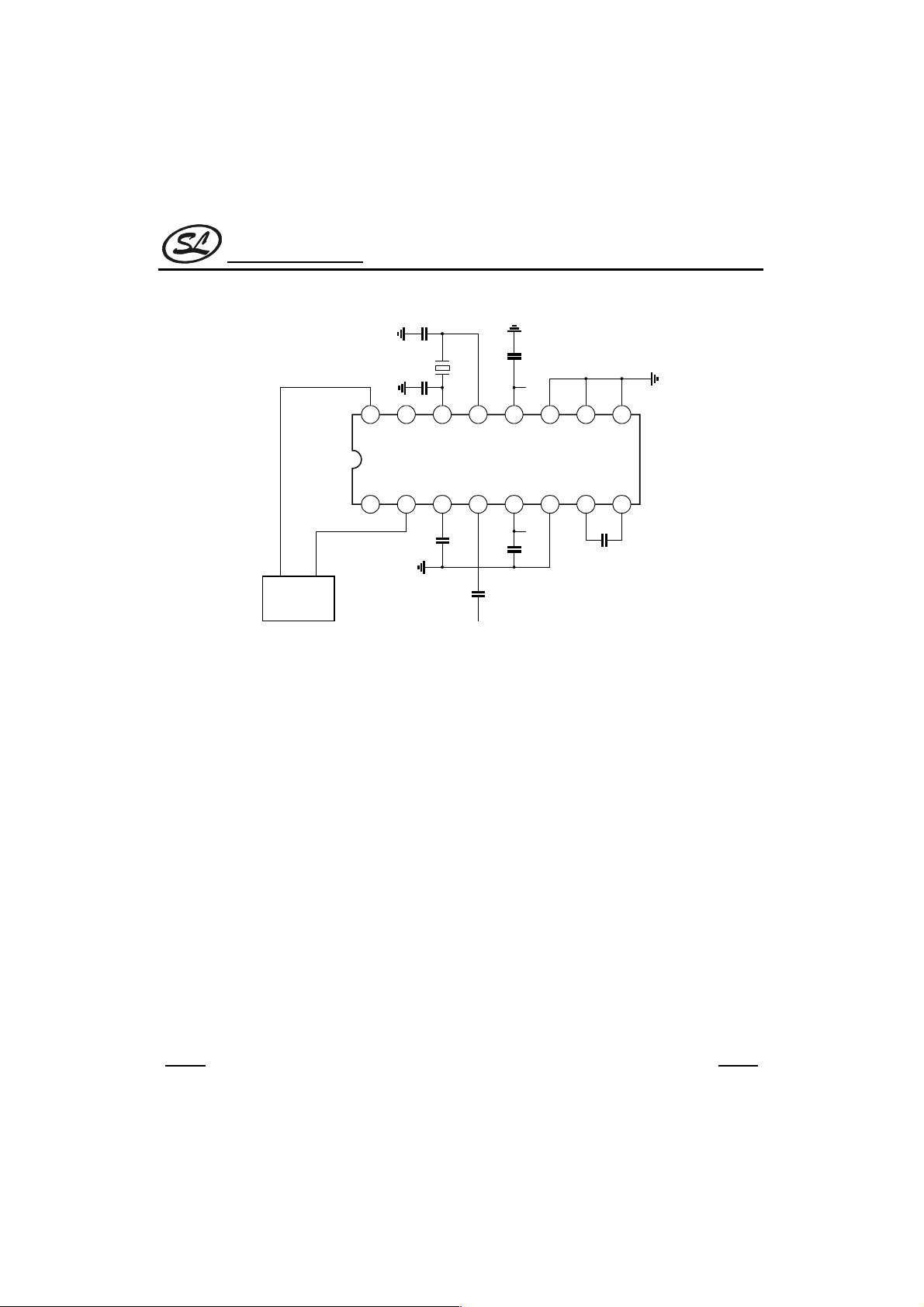
APPLICATION CIRCUIT
RDCL
RDDA
4.332/8.664MHz
47pF
82pF
16 15 14 13 12 11 10 9
SC6579
1 2 3 4 5 6 7 8
2.2F
0.1F
V
DDD
0.1F
V
DDA
560pF
SC6579
MPX signal
330pF
MCU
HANGZHOU SILAN MICROELECTRONICS JOINT-STOCK CO.,LTD
8
Rev: 1.0 2001.12.30
Page 9
Silan
Semiconductors
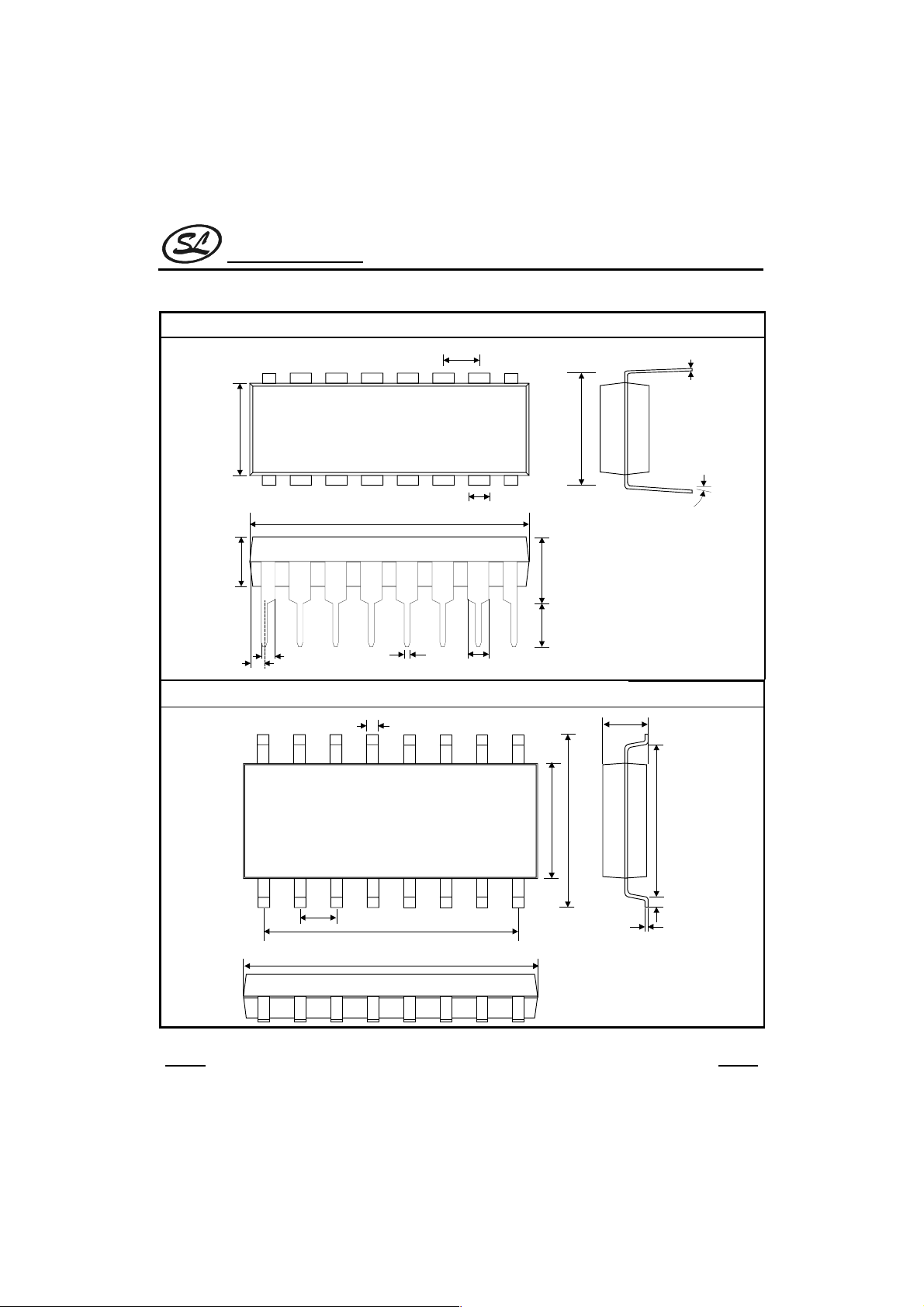
PACKAGE OUTLINE
DIP-16-300-2.54 UNIT: mm
2.54
SC6579
0.25B0.05
7.62
4.36 MAX
3.00 MIN
1.27 MAX
6.35B0.25
3.86
0.99
+0.3
-0
19.55
0.460.08
+0.2
-0.3
1.52
1.52
+0.3
-0
SOP-16-225-1.27 UNIT:mm
B
0.10
0.40
3.90B0. 3
1.80 MAX
-0.20
+0.40
6.0B0.4
5.0
1.27
10.15
8.89
+0.25
-0.20
0.20
+0.05
-0.02
0.50B0.20
HANGZHOU SILAN MICROELECTRONICS JOINT-STOCK CO.,LTD
9
Rev: 1.0 2001.12.30
 Loading...