

Page 1
Silan
a
Semiconductors
DIGITAL CONTROLLED STEREO
AUDIO PROCESSOR WITH LOUDNESS
DESCRIPTION
The SC7313 is a volume, tone (bass and treble), balance (left/
right) and fader(front/rear) processor for quality audio applications in
1
2
3
4
L
5
R
6
7
8
9
10
11
12
13
14
in and external
28
27
26
25
24
23
SC7313
22
21
20
19
18
17
16
15
car radio and Hi-Fi systems. Selectable input g
loudness function are provided. Control is accomplished by serial
2
C bus microprocessor interface. The AC signal settings is obtained
I
by resistor networks and switches combined with operational
amplifiers. Due to the Used BIPOLAR/CMOS technology, low
distortion, low noise andlow DC stepping are obtained.
FEATURES
* Input multiplexer:
--3 stereo inputs
--Selectable input gain for optimal adaptation to different
sources
* Four speaker attenuators:
--4 independent speakers control in 1.25dB steps for
balance and fader facilities
--Independent mute function
2
* All functions programmable via serial I
CBus
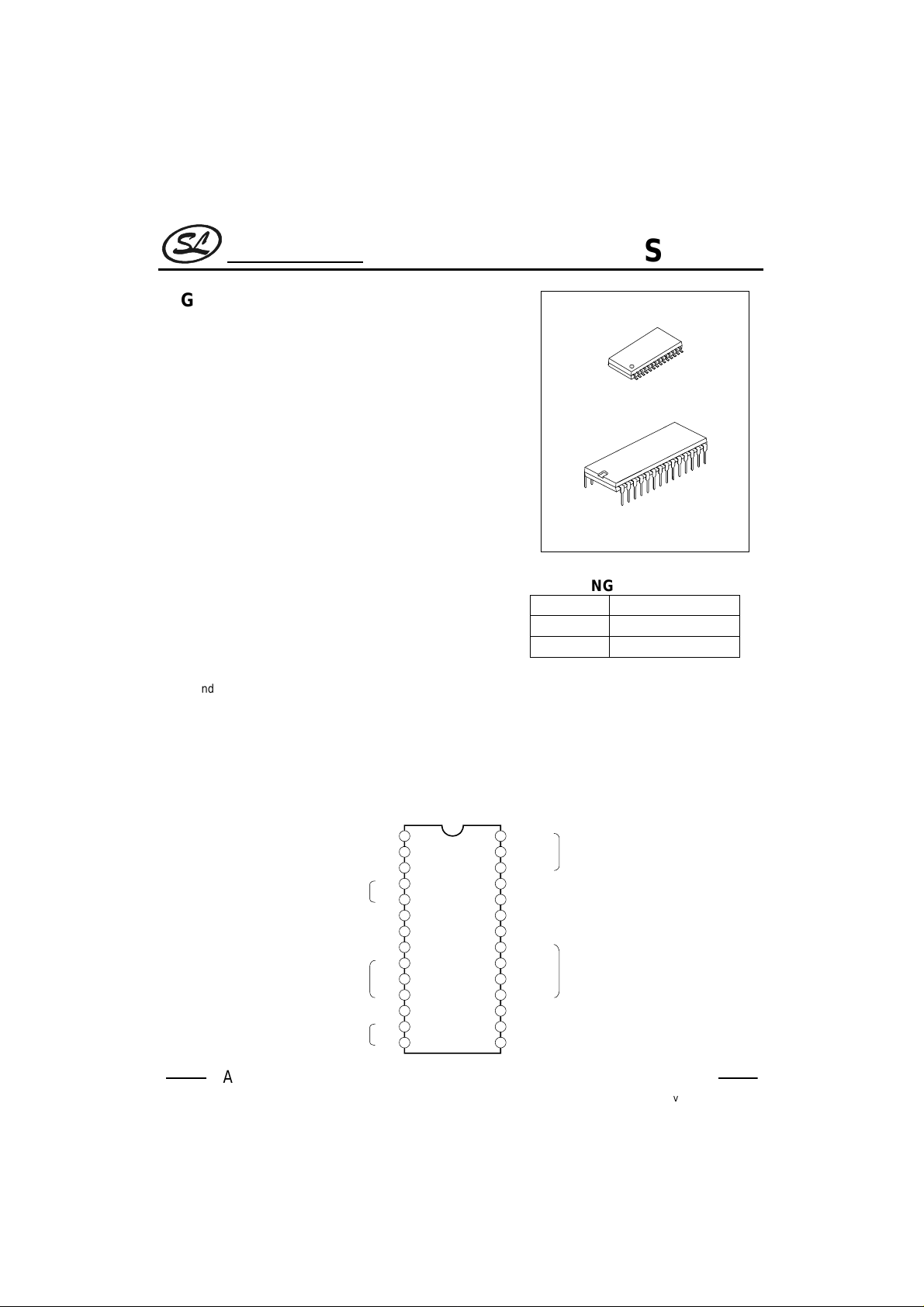
PIN CONFIGURATIONS
C
REF
DD
V
GND
TREBLE
IN(R)
OUT(R)
LOUD R
LEFT
R3
R2
R1
LOUD L
L3
L2
RIGHT
INPUTS
INPUTS
SC7313
SOP-28
DIP-28
ORDERING INFORMATION
Device Package
SC7313 DIP-28-600-2.54
SC7313S SOP-28-375-1.27
* Loudness function
* Volume control in 1.25dB steps
* Treble and bass control
* Input and output for external equalizer or
noise reduction system
SCL
SDA
DIG GND
OUT LF
OUT RF
OUT LR
OUT RR
BOUT(R)
BIN(R)
BOUT(L)
BIN(L)
OUT(L)
IN(L)
L1
BUS
INPUTS
BASS
) LEFT INPUTS
HANGZHOU SILAN MICROELECTRONICS JOINT-STOCK CO.,LTD
Rev: 1.1 2002.02.26
1
Page 2
Silan
Semiconductors
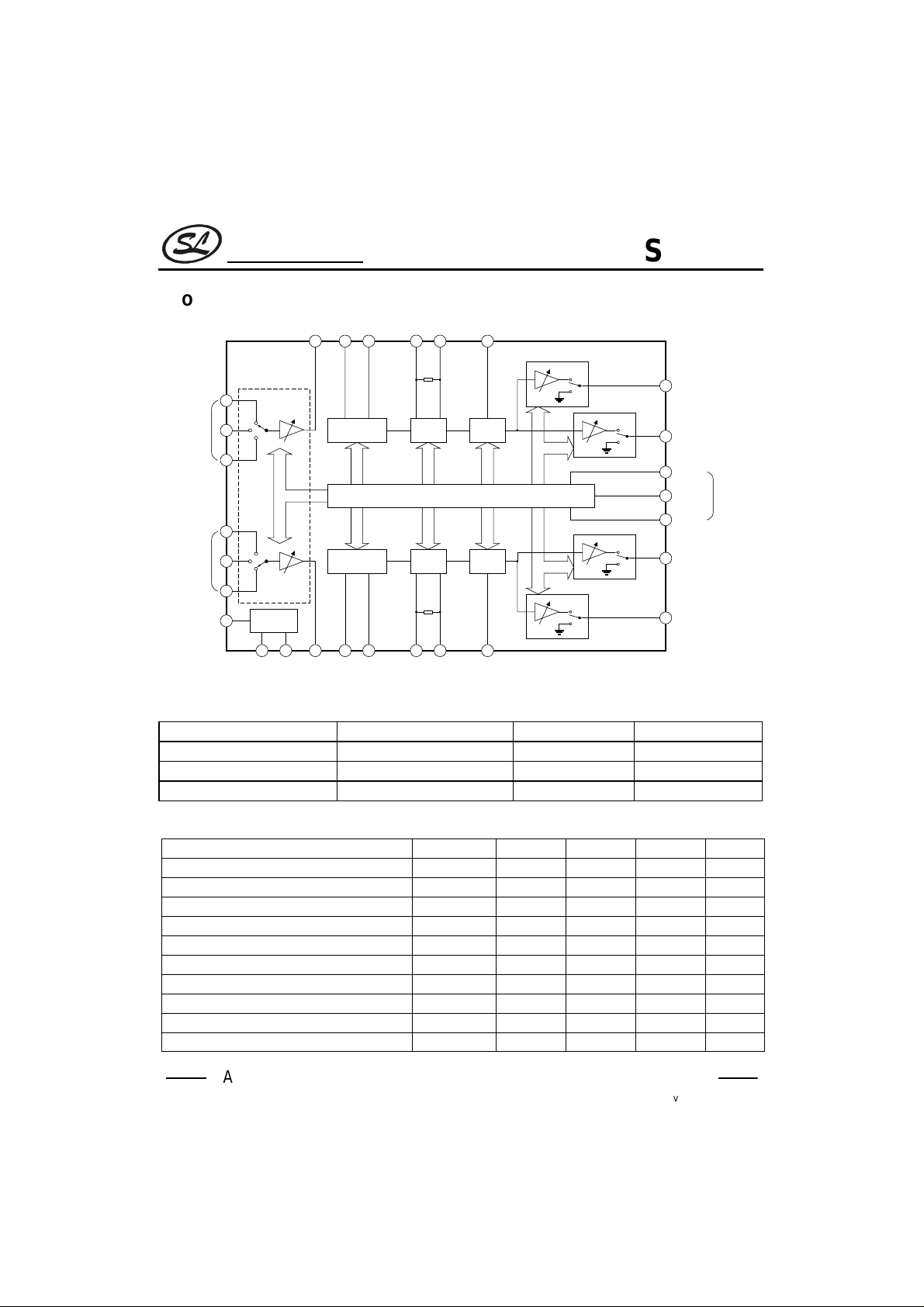
BLOCK DIAGRAM
B-OUT
(L)
(L)
(L)
BASS TREBLE
SERIALBUS DECODER +LATCHES
BASS TREBLE
B-IN
LOUDNESS
B-OUT
(R)
(R)
(R)
(L)
TREBLE
(R)
SPEAKER
ATT
MUTE
SPEAKER
ATT
MUTE
LEFT
INPUTS
RIGHT
INPUTS
CREF
INPUT SELECTION
& GAIN C ONTROL
15
14
13
9
10
11
SUPPLY1
2 3
VDD A-GND
LOUDNESS
IN
OUT
(L)
(L)
17 16 12 19 18 4
VOLUME
&LOUDNESS
VOLUME
&LOUDNESS
7 6 8 21 20 5
IN
OUT
(R)
(R)
TREBLE
B-IN
ABSOLUTE MAXIMUM RATINGS
Characteristic Symbol Value Unit
Supply Voltage V
S
10.2 V
Operating Temperature Tamb -40~ +85
Storage Temperature Tstg -55 ~ +150
QUICK REFERENCE DATA
Characteristic Symbol Min. Typ. Max. Unit
Supply Voltage Vs 6 9 10 V
Maximum input signal handling V
CL
Total harmonic distortion ,V=1Vrms, f=1kHz THD 0.01 0.1 %
Signal to noise ratio S/N 106 dB
Channel separation, f=1kHz Sc 103 dB
Volume control, 1.25dB step -78.75 0 dB
Bass and treble control, 2dB step -14 +14 dB
Fader and balance control, 1.25dB step -38.75 0 dB
Input gain, 3.75dB step 0 11.25 dB
Mute attenuation 100 dB
2Vrms
SC7313
25
SPEAKER
ATT
MUTE
SPEAKER
ATT
MUTE
23
28
27
26
24
22
LEFT
FRONT
OUT
LEFT
REAR
OUT
SCL
SDA
DIG-GND
RIGHT
FRONT
OUT
RIGHT
REAR
OUT
°C
°C
BUS
HANGZHOU SILAN MICROELECTRONICS JOINT-STOCK CO.,LTD
Rev: 1.1 2002.02.26
2
Page 3
Silan
Semiconductors
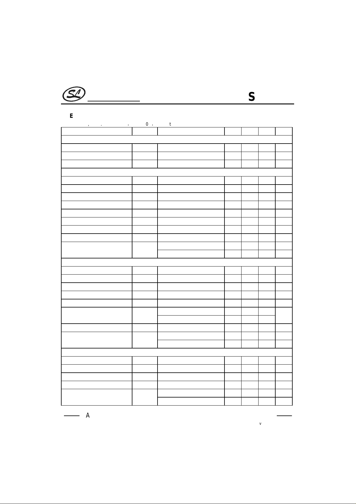
ELECTRICAL CHARACTERISTICS
(Refer to the test circuit)
(Tamb=25°CVS=9.0V,RL=10kΩRG=600Ωall controls flat(G=0), f=1kHz,Unless otherwise specified)
Parameter Symbol Test conditions Min Typ Max Unit
SUPPLY VOLTAGE
Operating Supply Voltage V
Operating Supply Current I
S
S
Ripple rejection of Supply Voltage SVR 60 80 dB
INPUTS SELECTORS
Input resistance R
Clipping Level V
Input Separation (note 2) S
Output load resistance R
Minimum input Gain G
Maximum input gain G
IN(MIN)
IN(MAX)
Step resolution G
Input noise e
DC steps V
Input 1,2,3 35 50 70
II
CL
IN
Pin7,17 4
L
STEP
G=11.25dB 2
IN
Adjacent gain steps 4 20 mV
DC
G=18.75 to MUTE 4 mV
VOLUME CONTROL
Input resistance R
IV
Control range Crange 70 75 80 dB
Minimum attenuation A
Maximum attenuation A
Step resolution A
Attenuation set error E
Tracking error E
DC steps V
V(min)
V(max)
STEP
A
T
DC
AV=0 to –20dB -1.25 0 1.25
AV=-20 to –60dB -3 2
Adjacent attenuation steps 0 3 mV
From 0dB to AVmax 0.5 7.5 mV
SPEAKER ATTENUATORS
Control Range Crange 35 37.5 40 dB
Step resolution S
Attenuation Set error E
Output Mute Attenuation A
DC steps V
STEP
A
MUTE
Adjacent attenuation steps 0 3 mV
DC
From 0dB to MUTE 1 10 mV
0.5 1.25 1.75 dB
0.5 1.25 1.75 dB
SC7313
6 9 10.0 V
20.0 35.0 mA
kΩ
22.5 Vrms
80 100 dB
kΩ
-1 0 1 dB
11.25 dB
3.75 dB
µV
20 33 50
-1 0 1 dB
70 75 80 dB
80 100 dB
kΩ
dB
2dB
1.5 dB
HANGZHOU SILAN MICROELECTRONICS JOINT-STOCK CO.,LTD
Rev: 1.1 2002.02.26
3
Page 4
Silan
Semiconductors
(continued)
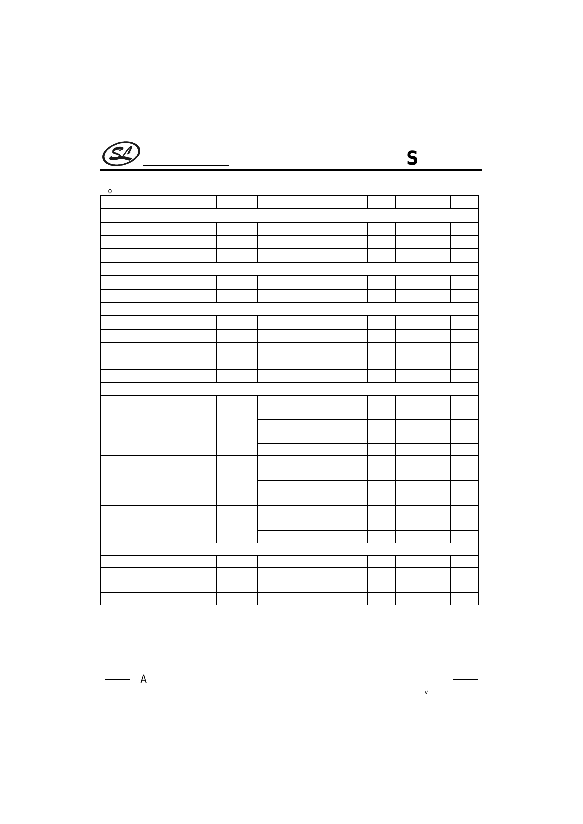
Parameter Symbol Test conditions Min Typ Max Unit
BASS CONTROL (note 1)
Control Range G
Step resolution B
Internal feedback resistance R
TREBLE CONTROL (note 1)
Control Range Gt Maximum boost/cut
Step resolution T
AUDIO OUTPUTS
Clipping level V
Output load resistance R
Output load capacitance C
Output resistance R
DC voltage level V
GENERAL
Output noise e
Signal to noise ratio S/N All gains=0dB; Vo=1Vrms 106 dB
Distortion d
Channel separation left/right Sc 80 103 dB
Total tracking error
BUS INPUTS
Input low voltage V
Input high voltage V
Input current I
Output voltage SDA acknowledge Vo Io=1.6mA 0.4 V
NOTES:
(1) Bass and treble response see Figure 16. The center frequency and quality of the response behavior can be
chosen by the external circuitry. A standard first order bass response can realized by a standard feedback
network.
(2) The selected input is grounded through the 2.2µF capacitor.
Maximum boost/cut
B
STEP
B
STEP
THD=0.3% 2 2.5 Vrms
OCL
L
L
OUT
OUT
BW=20 ~20kHz,flat
output muted
NO
BW=20 ~20kHz,flat
All gains=0dB
A curve, all gains =0 dB 3
Av=0,VIN=10mV 0.01 0.1 %
Av=-20dB, VIN=1Vrms 0.09 0.3 %
Av=-20dB,V
AV=0 to –20 dB 0 1 dB
AV=-20 to –60 dB 0 2 dB
IL
IH
IN
=0.3Vrms 0.04 %
IN
±12 ±14 ±16
±13 ±14 ±15
4.2 4.5 4.8 V
SC7313
dB
123dB
34 44 58
123dB
4
30 75 120
2.5
515
3V
-5 +5
kΩ
dB
kΩ
10 nF
Ω
µV
µV
µV
1V
µA
HANGZHOU SILAN MICROELECTRONICS JOINT-STOCK CO.,LTD
Rev: 1.1 2002.02.26
4
Page 5

Silan
Semiconductors
TYPICAL CHARACTERISTICS PERFORMANCE
Fig.1 Loudness vs. Volume
Attention
20
15
10
Loudness (dB)
5
0
01020304050
Volume Attention (dB)
Fig.2 Loudness vs. Frequency vs.
volume Attenuation
20
0
-20
Loudness (dB)
-40
-60
100 1k 10k
Frequency (Hz)
C
LOUD=
100nF
SC7313
Fig.3 Loudness vs. External
Capacitors
-10
56nF
10nF
100nF
Frequency (Hz)
OPEN
-20
220nF
-30
Loudness (dB)
Shortedto VREF
-40
10 100 1k 10k 100k
Fig.4 Noise vs.Volume/Gain
10
Noise (µV
3
1
-80 -60 -40 0-20
Fig.7 Distortion & Noise vs.
1
VIN=250mVrms
AV=0dB
All controls Flat
-1
10
-2
10
THD & Noise (%)
-3
10
100 1k 10k 100k10
settings
22Hz ~ 22kHz
ACurve
Volume (dB)
Frequency
Volume=-20dB
Volume=0dB
Frequency (dB)
Fig.5 Signal to Noise Ratio
vs.Volume settings
1V
100k
10k
1k
Noise (µV
100
10
1
-80
VIN=1V
S/N=106dB
-60 -40 -20 0 20
Volume (dB)
Fig.8 Distortion vs. Load
-1
10
Resistance
THD (%)
-2
10
0.1 1
Load Resistance (kΩ)
S/N=76dB
VIN=316V
Fig.6 Distortion &Noise vs.
VIN=1Vrms
AV=0dB
All controls Flat
100 1k 10k 100k10
Frequency
Volume=-20dB
Volume=0dB
1
-1
10
-2
10
THD & Noise (%)
-3
10
Frequency (dB)
Fig.9 Channel Separation(L→R) vs.
110
100
90
80
Frequency
VIN=1Vrms
AV=0dB
All controls Flat
Channel Separation(dB)
70
10110210
3
Frequency (Hz)
4
10
HANGZHOU SILAN MICROELECTRONICS JOINT-STOCK CO.,LTD
Rev: 1.1 2002.02.26
5
Page 6

Silan
Semiconductors
TYPICAL CHARACTERISTICS PERFORMANCE
Fig.10 Input Separation
(L1→L2,L3,L4) vs. Frequency
110
Fig.11 Supply Voltage Rejection
100
vs. Frequency
(continued)
SC7313
Fig.12 Output Clipping Level vs.
Supply Voltage
100
90
80
VIN=1Vrms
AV=0dB
All controls Flat
Channel Separation(dB)
70
2
10110
Fig.13 Quiescent current vs. Supply
8.0
6.0
Quiescent Current (mA)
4.0
2.0
46 810 12
10310
Frequency (Hz)
Voltage
Supply Voltage (V)
90
80
70
Channel Separation(dB)
60
4
9.0
8.5
8.0
7.5
Quiescent Current (mA)
7.0
6.5
15
10
5
0
-5
Tone Response (dB)
-10
-15
Vsvr=0.5Vrms
All Input toGND
AV=0dB
All controls Flat
()
k
10310
4
4
10110210310
Frequency (Hz)
Fig.14 Supply current vs.
Temperature
Vs=9V
-60 -30 0 30 60 90
Temperature
Fig.16 Typical Tone Response
(with the Extcomponents indicated
the test circuit)
AV=0dB
1
2
10
10
Frequency (Hz)
5.0
4.0
3.0
Output Clipping Level (v)
2.0
1.0
50
48
46
44
Bass Resistance (kΩ
42
40
RL=10kΩ
f=1kHz
THD=0.3%
46 810 12
Supply Voltage (V)
Fig.15 Bass resistance vs.
Temperature
-60 -30 0 30 60 90
Temperature
()
k
HANGZHOU SILAN MICROELECTRONICS JOINT-STOCK CO.,LTD
Rev: 1.1 2002.02.26
6
Page 7

Silan
Semiconductors
APPLICATION NOTES
1. I2C BUS INTERFACE
Data transmission from microprocessor to the SC7313 and viceversa takes place through the 2 wires I
interface, consisting of the two lines SDAand SCL(pull-up resistors to positive supply voltage must be connected).
2. DATA VALIDITY
As shown in Figure 17, the data of the SDA line must be stable during the high period of the clock. The HIGH
and LOW state of the dtat line can only change when the clock signal on the SCL line is LOW.
SDA
SCL
SC7313
2
CBUS
DATA LINE
STABLE, DATA
VALID
CHANGE
DATA
ALLOWED
2
Fig. 17 Data Validity on the I
CBUS
3. START AND STOP CONDITI O NS
As shown in Figure 18, a start condition is a HIGH to LOW transition of the SDA line while SCL is HIGH. The
stop condition is a LOW to HIGH transition of the SDA line while SCL is HIGH.
SCL
SDA
start stop
//
//
2
I
BUS
C
2
Fig. 18 Timing diagram of I
CBUS
4. BYTE FORMAT
Every byte transferred on the SDA line must obtain 8 bits. Each byte must be followed by the an acknowledge
bit. The MSB is transferred first.
HANGZHOU SILAN MICROELECTRONICS JOINT-STOCK CO.,LTD
Rev: 1.1 2002.02.26
7
Page 8

Silan
Semiconductors
5. ACKNOWLEDGE
The master(microprocessor) puts a resistive HIGH level on the SDA line during the acknowledge clock
pulse(see Figure 19). The peripheral(audioprocessor) that acknowledges has to pull-down(LOW) the SDA line
during the acknowledgeclock pulse, so that the SDA line is stable LOW during this clock pulse.
The audioprocessor which has been addressed has to generate an acknowledge after the reception of each
byte , otherwise the SDA line remain at the HIGH level during the ninth clock pulse time. In this case the master
transmitter can generate the STOPinformation in order to abort the transfer.
SC7313
SCL
SDA
start
6. TRANSMISSION WITHOUT ACKNOWLEDGE
Avoiding to detect the acknowledge of the audioprocessor, the microprocessor can use a simpler transmission:
simply it waits one clock without checking the slave acknowledgig, and sends the new data.
This approach of course is less protected from mis-working and decreases the noise immunity.
123789
MSB
Fig. 19 Acknowledge on the I
//
//
2
CBUS
Acknowledgment
from receiver
SOFTWARE SPECIFICATION
1. Interface protocol
The interface protocol comprises:
A start conditions
A chip address byte, containing the SC7313 address(the 8thbit of the bytes must be 0). The SC7313
must always acknowledge at the end of each transmitted byte.
A sequence of data(N-bytes + acknowledge)
A stop condition (P)
SC7313 address
MSB LSB
S 1 0 0 0 1 0 0 0 ACK DATA ACK DATA P
MSB LSB MSB LSB
ACK
ACK: Acknowledge
S: Start
P: Stop
Max clockspeed: 100kbits/sec
Data Transferred
(N-Bytes +Acknowledge)
HANGZHOU SILAN MICROELECTRONICS JOINT-STOCK CO.,LTD
Rev: 1.1 2002.02.26
8
Page 9

Silan
Semiconductors
2. Chipsaddress
1(MSB)0001000(LSB)
3. Data bytes
MSB LSB Function
0 0 B2 B1 B0 A2 A1 A0 Volume Control
1 1 0 B1 B0 A2 A1 A0 Speaker ATT LR
1 1 1 B1 B0 A2 A1 A0 Speaker ATT RR
1 0 0 B1 B0 A2 A1 A0 Speaker ATT LF
1 0 1 B1 B0 A2 A1 A0 Speaker ATT RF
0 1 0 G1G0S2S1S0Audioswitch
0 1 1 0 C3 C2 C1 C0 Bass control
0 1 1 1 C3 C2 C1 C0 Treble control
Note: Ax=1.25dB steps;Bx=10dB steps;Cx=2dB steps;Gx=3.75dB steps
DETAILED DESCRIPTION OF DATA B YTES
1. Volume
MSB LSB Function
0 0 B2 B1 B0 A2 A1 A0 Volume 1.25dB steps
000 0
001 -1.25
010 -2.5
011 -3.75
100 -5
101 -6.25
110 -7.5
111 -8.75
0 0 B2 B1 B0 A2 A1 A0 Volume 10dB steps
000 0
001 -10
010 -20
011 -30
100 -40
101 -50
110 -60
111 -70
For example, a volume of –45dB is given by: 00100100
SC7313
HANGZHOU SILAN MICROELECTRONICS JOINT-STOCK CO.,LTD
Rev: 1.1 2002.02.26
9
Page 10

Silan
Semiconductors
2. speaker attenuators
MSB LSB Function
1 0 0 B1 B0 A2 A1 A0 Speaker ATT LF
1 0 1 B1 B0 A2 A1 A0 Speaker ATT RF
1 1 0 B1 B0 A2 A1 A0 Speaker ATT LR
1 1 1 B1 B0 A2 A1 A0 Speaker ATT RR
000 0
001 -1.25
010 -2.5
011 -3.75
100 -5
101 -6.25
110 -7.5
111 -8.75
00 0
01 -10
10 -20
11 -30
11111 MUTE
For example, attenuation of 25dB on speaker RF is given by: 10110100
SC7313
4. Audioswitch
MSB LSB Function
0 1 0 G1G0S2S1S0 Audioswitch
0 0 Stereo 1
0 1 Stereo 2
1 0 Stereo 3
1 1 Stereo 4
0 Loudness ON
1 Loudness OFF
0 0 +11.25dB
0 1 +7.5dB
1 0 +3.75dB
1 1 0dB
For example, to select the stereo 2 input with a gain of +7.5dB Loudness ON the 8bit string is: 01001001
Note: Stereo4 is connected internally, but not available on pins.
HANGZHOU SILAN MICROELECTRONICS JOINT-STOCK CO.,LTD
Rev: 1.1 2002.02.26
10
Page 11

Silan
Semiconductors
5.Bass and treble
MSB LSB Function
0 1 1 0 C3 C2 C1 C0 Bass
0 1 1 1 C3 C2 C1 C0 Terble
0000 -14
0001 -12
0010 -10
0011 -8
0100 -6
0101 -4
0110 -2
0111 0
1111 0
1110 2
1101 4
1100 6
1011 8
1010 10
1001 12
1000 14
C3=Sign
For Example, bass at –10dB is obtained by the following 8bit string is: 01100010.
TEST AND TYPICAL APPLICATION CIRCUIT
SC7313
¡
5.6k
100
100nF100
nF
BOUT
(L)
(L)
BOUT
(R)
100
100
nF
nF
2.7nF
nF
BIN
TREBLE
(L)
(L)
2.7nF
10F
25
F
10
24
F
10
23
F
10
22
OUT LF
OUT RF
OUT LR
OUT LR
BIN
TREBLE
(R)
(R)
100
nF
5.6k
¡
AM/FM
TUNER
CD
PLAYER
TAPE
MCU
28 27 26
DGND SDA SCL
R1
11
2.2
F
L1
15
2.2
F
R2
10
2.2
F
L2
14
2.2
F
R3
9
2.2
F
L3
13
F
2.2
V
DD
VDDAGND C
2 3 1
2.2F
17 16 12 19 18 4
OUT(L) IN(L)
SC7313
REF
OUT(R) IN(R)
7 6 8 21 20 5
22F
F
2.2
LOUD
LOUD
(R)
HANGZHOU SILAN MICROELECTRONICS JOINT-STOCK CO.,LTD
Rev: 1.1 2002.02.26
11
Page 12

Silan
2
Semiconductors
PACKAGE OUTLINE
DIP-28-600-2.54 UNIT:mm
2.54
0.25
B
13.8
SC7313
0.05
B
0.25
15.24(600)
37.34B0.3
0.5MIN
0.46B0.08
1.52B0.5
4.96MAX
3.00MIN
.16MAX
15 degree
SOP-28-375-1.27 UNIT:mm
0.3
0.4
B
B
17.75B0.25
16.51
1.27
0.45
7.6
10.2
B
0.1
2.8 MAX
9.525(375)
0.15B0.05
HANGZHOU SILAN MICROELECTRONICS JOINT-STOCK CO.,LTD
Rev: 1.1 2002.02.26
12
Page 13
Silan
Attach
Semiconductors
SC7313
Revision History
Data REV Description Page
2000.12.31 1.0 Original
2002.02.26 1.1 Modify the “package outline” 12
HANGZHOU SILAN MICROELECTRONICS JOINT-STOCK CO.,LTD
Rev: 1.1 2002.02.26
13
 Loading...