

Page 1
Silan
Semiconductors
INFRARED REMOTE CONTROL
TRANSMITTER
DESCRIPTION
The SC6122 is a remote control transmitter utilizing CMOS
Technology specially designed for use on infrared remote control
applications. It is capable of controlling 64 function keys and 3
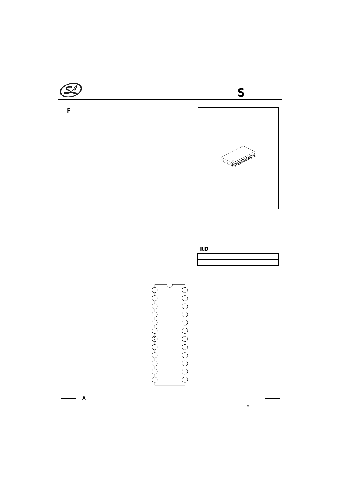
double keys. SC6122 is housed in a 24-pins SO package.
FEATURES
* CMOS Technology
* Low Operating Voltage (V
* Using SEL pin, SC6122 can support 128+6 function codes
* Customer Code can be selected
APPLICATIONS
* TV and VCR
* Audio Equipment
* Air Conditioner
* VCD and DVD ROM/Player
* Moniputer/Multi-Media Personal Computer System
PIN CONFIGURATION
=2.0~5.5V)
DD
KI2
KI3
KI4
KI5
KI6
KI7
REM
V
DD
SEL
OSCO
OSCI
V
ss
1
2
3
4
5
6
7
8
9
10
11
12
SC6122
24
23
22
21
20
19
18
17
16
15
14
13
SC6122
ORDERING INFORMATION
SC6122-001
SC6122-002
KI1
KI0
CCS
KI/O0
KI/O1
KI/O2
KI/O3
KI/O4
KI/O5
KI/O6
KI/O7
LMP
ROM Content=0
Custom Version
SOP-24
HANGZHOU SILAN MICROELECTRONICS JOINT-STOCK CO.,LTD
Rev: 2.2 2002-03-01
1
Page 2
Silan
Semiconductors
BLOCK DIAGRAM
KI0
23
KI1
24
OSCI OSCO V
1011 8 12
OSC Circuit
SC6122
DD
Vss
SEL
9
KI2
KI3
KI4
KI5
KI6
KI7
1
Key
2
3
Input
Scan
Circuit
4
5
6
Timing
Generation
&Control Circuit
Code Generation Circuit
Key Input/Output Scan Circuit
Optput
Control
Circuit
13
22
REM
7
LMP
CSS
2021 1819 1617 1415
KI/O0 KI/O1 KI/O2 KI/O3 KI/O4 KI/O5 KI/O6 KI/O7
ABSOLUTE MAXIMUM RATING
(Tamb=25°C, unless otherwise specified)
Characteristic Symbol Value Unit
Supply Voltage V
Input Voltage V
Power Dissipation Pd 250 mW
Storage Temperature T
Operating Temperature T
DD
IN
stg
opr
6.0 V
-0.3~VDD V
-40~+125
-20~+75
°C
°C
RECOMMENDED OPERATING CONDITIONS
(Tamb=25°C,unless otherwise specified)
Characteristic Symbol Min. Typ. Max. Unit
Supply Voltage V
Oscillation Frequency fosc 400 455 500 KHz
Input Voltage V
Custom Code Select Pull-Up
Resistance
DD
IN
Rup -- 100 --
2.0 3.0 3.3 V
0--VDDV
KΩ
HANGZHOU SILAN MICROELECTRONICS JOINT-STOCK CO.,LTD
Rev: 2.2 2002-03-01
2
Page 3
Silan
Semiconductors
ELECTRICAL CHARACTERISTICS
Parameter Symbol Test conditions Min Typ Max Unit
Supply Voltage V
Current Consumption 1 I
Current Consumption 2 I
REM High Level Output Current I
REM Low Level Output Current I
LMP High Level Output Current I
LMP Low Level Output Current I
KI High Level Input Current I
KI Low Level Input Current I
KI High Level Input Voltage V
KI Low Level Input Voltage V
KI/O High Level Input Voltage V
KI/O Low Level Input Voltage V
KI/O High Level Input Current I
KI/O Low Level Input Current I
KI/O High Level Output Current I
KI/O Low Level Output Current I
CCS Low Level Input Voltage V
CCS High Level Input Current I
CCS Low Level Input Current I
CCS High Level Input Current I
CCS Low Level Input Current I
PIN DESCRIPTION
Pin No. Symbol I/O Description
23,24,1~6 KI0~KI7 I Key Input Pin Nos. 0~7
7 REM O Data Output Pin
8VDD-- Power Supply
9 SEL I Select Pin
10 OSCO O Oscillator Pin
11 OSCI I Oscillator Pin
12 Vss -- Power Supply
13 LMP -- Output LED Indicator
21~14 KI/O0~KI/O7 I/O Key Input/Output Pin Nos.0~7
22 CCS I Custom Code Scan Input Pin
DD1
DD2
OH1
OL1
OH2
OL2
OH3
OL3
IH1
IL1
IH2
IL2
IH3
IL3
IH4
IL4
(Tamb=25°C,VDD=3.0V,unless otherwise specified)
DD
Fosc =455KHz 0.1 1.0 mA
Fosc =STOP 1.0
Vo=1.5V -5.0 -8.0 mA
Vo=0.3V 15 30
Vo=2.7V -15 -30
Vo=0.3V 1 1.5 mA
VIN=3.0V 5 30
VIN=0V -0.2
IH1
IL1
IH2
IL2
VIN=3.0V 2 7
VIN=0V -0.2
Vo=2.5V 0.5 1.5 mA
Vo=1.7V 1.5 2.5 mA
IH3
Pull Up VIN=3.0V 0.2
Pull Up VIN=0V -3 -15
Pull Down VIN=3.0V 5 30
Pull Down VIN=0V -0.2
SC6122
2.0 3.0 5.5 V
µA
µA
µA
µA
µA
0.7 V
DD
00.3V
0.7 V
DD
00.4V
1.1 V
V
V
DD
DD
DD
V
V
V
µA
µA
µA
µA
µA
µA
HANGZHOU SILAN MICROELECTRONICS JOINT-STOCK CO.,LTD
Rev: 2.2 2002-03-01
3
Page 4
Silan
Semiconductors
FUNCTIONAL DESCRIPTION
1. TRANSMISSION CODE
The transmission code consists of a leader code, 16-bits custom codes, and 8-bits data codes. The inverse
code of the data code is also sent simultaneously. The following diagram shows this one frame construction.
C0'
C0'
C0 C1 C2 C3 C5C4 C6 C7
Leader
Code
Custom Code
8bits
The leader codes consist of a 9ms carrier waveform followed by a 4.5ms OFF waveform. It is used as the leader
for the following code. Thus, when reception is configured by a microcomputer, the time relationship between the
reception detection and other processes can be managed efficiently. The code uses the PPM (Pulse Position
Modulation) Method, with "0" and "1" differentiated by the time between pulses. Each code consists of 8 bits, and
simultaneous transmission of the inverse code allows configuration of a system with an extremely low error rate.
2. KEY INPUT MATRIX
The Key Input Matrix of SC6122 if given below:
C0'C2C0'C3C0'C4C0'C5C0'C6C0'
C0
C1
Custom Code'
KI/O0
8bits
D0 D1 D2 D3 D4 D0 D1 D2 D3 D4 D5 D6 D7
C7
KI/O1
KI/O2
KI/O3
KI/O4
KI/O5
Key Data
8bits
KI/O6
D5 D6 D7
KI/O7
SC6122
Key Data
8bits
KI0
KI1
KI2
KI3
KI4
KI5
KI6
KI7
51 139 2117 2925
62 1410 2218 3026
73 1511 2319 3127
84 1612 2420 3228
3733 4541 5349 6157
3834 4642 5450 6258
3935 4743 5551 6359
4036 4844 5652 6460
3. KEY INPUT
A total of 64 keys can be connected by SC6122 Key Input Pins--KI0~KI7 and the Timing Signal Output Pins
KI/O0~KI/O7.
Double Key Operation is possible for only Key No.21 in combination with other keys connected to the KI/O5 line
namely: Key No.22,23 or 24.thus, only the following key combinations may be used for the double key operation:
1. Key Nos.21 and 22 ; 2. Key Nos.21 and 23 ; 3. Key Nos.21 and 24
HANGZHOU SILAN MICROELECTRONICS JOINT-STOCK CO.,LTD
Rev: 2.2 2002-03-01
4
Page 5

Silan
Semiconductors
Pull-down resistors are connected between the Key Input and Vss Pins. When more than one key (except the
double key combinations:K21+22, K21+23, K21+24) are pressed simultaneously, the transmission output stops.
Two key inputs are regarded as being pressed simultaneously when the time interval between these two key
entries is less than 36ms.
The order of priority given to two key inputs with a time interval of more than 36ms is on a First-Pressed-First-
Served or Longer-Pressed-First-Served Basis.
When a key is pressed, the custom and data codes are read. 36ms later, the Remote (REM) Output is activated.
When the key is kept depressed during this 36ms, one transmission is outputted. If the key is depressed for more
than 108ms, then the only the leader code is transmitted continuously.
4. DOUBLE KEY OPERATION
Double Key Operation is useful for operations such as tape deck recording. The following table shows the Key
Data corresponding to the double keys pressed. Also refer to the Key Input Section.
The Double Key operation forms are as follows:
Key D0 D1 D2 D3 D4 D5 D6 D7
K21+K2210101100/1
K21+K2301101100/1
K21+K2411101100/1
Note: D7=1 when SEL is connected to VSS, or D7=0 when SEL is connected to VDD.
SC6122
K21
D5+K22 to 24
Transmission
No Transmission
No Transmission
OPERATION
K21
push
NO OPERATION
K21
NO OPERATION
K21
NO OPERATION
K22 to 24
K21 Transmission
t >126ms
K22to24
push
K21 Transmission
36ms< t <126ms
K22to24
No Transmission
-36ms< t < 36ms
K22 to 24
t >126ms
K22 to 24 Transmission
HANGZHOU SILAN MICROELECTRONICS JOINT-STOCK CO.,LTD
Rev: 2.2 2002-03-01
5
Page 6

Silan
Semiconductors
5. REMOTE OUTPUT WAVEFORMS
The Remote Output Waveforms are given in the diagram below:
Key ON
1
Min.
36ms
Ex. fosc=455KHz
1
58.5 to 76.5ms
108ms
2 3
SC6122
108ms
9ms
13.5ms
Leader
Code
2
3
Custom Code
4.5ms
8bits
18ms to 36ms 27ms
9ms 4.5ms
13.5ms
9ms
11.25ms
Custom
Code
58.5ms to 76.5ms
1.125ms
2.25ms
0.56ms
Data Code
8bits
0.56ms
2.25ms
Data Code
8bits
000111
Carrier
8.77µs
26.3µs
CarrierFrequency---Fc=fosc/12=38KHz
9ms to 0.56ms
HANGZHOU SILAN MICROELECTRONICS JOINT-STOCK CO.,LTD
Rev: 2.2 2002-03-01
6
Page 7

Silan
Semiconductors
SC6122 KEYS DATA CODE
The Keys Data Code is given in the table below.
Connection Data Code Key
No.
KI0 KI1 KI2 KI3 KI/O D0 D1 D2 D3 D4 D5 D6 D7
K1
K2
K3
K4
K5
K6
K7
K8
K9
K10
K11
K12
K13
K14
K15
K16
K17
K18
K19
K20
K21
K22
K23
K24
K25
K26
K27
K28
K29
K30
K31
K32
•
•
•
•
•
•
•
•
•
•
•
•
•
•
•
•
•
•
•
•
•
•
•
•
•
•
•
•
•
•
•
•
KI/O0
KI/O1
KI/O2
KI/O3
KI/O4
KI/O5
KI/O6
KI/O7
SC6122
00000000/1
10000000/1
01000000/1
11000000/1
00100000/1
10100000/1
01100000/1
11100000/1
00010000/1
10010000/1
01010000/1
11010000/1
00110000/1
10110000/1
01110000/1
11110000/1
00001000/1
10001000/1
01001000/1
11001000/1
00101000/1
10101000/1
01101000/1
11101000/1
00011000/1
10011000/1
01011000/1
11011000/1
00111000/1
10111000/1
01111000/1
11111000/1
(to be continued)
HANGZHOU SILAN MICROELECTRONICS JOINT-STOCK CO.,LTD
Rev: 2.2 2002-03-01
7
Page 8

Silan
Semiconductors
(continued)
Connection Data Code Key
No.
KI4 KI5 KI6 KI7 KI/O D0 D1 D2 D3 D4 D5 D6 D7
K33
K34
K35
K36
K37
K38
K39
K40
K41
K42
K43
K44
K45
K46
K47
K48
K49
K50
K51
K52
K53
K54
K55
K56
K57
K58
K59
K60
K61
K62
K63
K64
Note: D7=1 when SEL is connected to VSS, or D7=0 when SEL is connected to VDD.
•
•
•
•
•
•
•
•
•
•
•
•
•
•
•
•
•
•
•
•
•
•
•
•
00000010/1
KI/O0
•
KI/O1
•
KI/O2
•
KI/O3
•
KI/O4
•
KI/O5
•
KI/O6
•
KI/O7
•
10000010/1
01000010/1
11000010/1
00100010/1
10100010/1
01100010/1
11100010/1
00010010/1
10010010/1
01010010/1
11010010/1
00110010/1
10110010/1
01110010/1
11110010/1
00001010/1
10001010/1
01001010/1
11001010/1
00101010/1
10101010/1
01101010/1
11101010/1
00011010/1
10011010/1
01011010/1
11011010/1
00111010/1
10111010/1
01111010/1
11111010/1
SC6122
HANGZHOU SILAN MICROELECTRONICS JOINT-STOCK CO.,LTD
Rev: 2.2 2002-03-01
8
Page 9

Silan
Semiconductors
TYPICAL APPLICATION CIRCUIT
VDD
F47F
0.1
11 10 8 13 7
KI0
23
KI1
24
KI2
1
KI3
2
KI4
3
KI5
4
KI6
5
KI7
KI/O0 KI/O2 KI/O3 KI/O4 KI/O5KI/O1 KI/O6 KI/O7
6
21 20 19 18 17 16 15 14
455KHz
200pF200pF
OSCOOSCI
SC6122
SC6122
DD
V
IR LED
470
¡
LED
270
¡
DD
REMLMPV
47F
1
¡
V
DD
SEL
9
SS
V
12
CCS
22
IN4148
IN4148
IN4148
IN4148
IN4148
IN4148
IN4148
For Custom
Code Selection
¡
100K¡100K¡100K¡100K¡100K¡100K¡100K
¡
100K
IN4148
DD
V
Note:1. Two capacitance connect with Vcc should as near as possible.
2. The line between two capacitance and Vcc and ground should as short as possible.
HANGZHOU SILAN MICROELECTRONICS JOINT-STOCK CO.,LTD
Rev: 2.2 2002-03-01
9
Page 10

Silan
Semiconductors
CHIP TOPOGRAPHY
SC6122
Size: 1.84 x 1.46 mm
2
PAD COORDINATES
No. Symbol X Y No. Symbol X Y
1 P1 -602.80 -322.10 13 P13 605.70 217.90
2 P2 -602.80 -452.10 14 P14 542.00 452.00
3 P3 -350.70 -452.10 15 P15 403.50 452.00
4 P4 -220.90 -452.10 16 P16 160.40 452.00
5 P5 -89.50 -452.10 17 P17 12.50 452.00
6 P6 41.00 -452.10 18 P18 -230.30 452.00
7 P7 171.40 -452.10 19 P19 -361.30 451.90
8 P8 347.90 -452.10 20 P20 -602.50 451.90
9 P9 477.80 -452.10 21 P21 -607.50 252.40
10 P10 608.00 -452.10 22 P22 -602.80 68.50
11 P11 607.20 -176.00 23 P23 -602.80 -61.20
12 P12 607.20 -44.60 24 P24 -602.80 -191.50
Note: The original point of the coordinate is the die center.
HANGZHOU SILAN MICROELECTRONICS JOINT-STOCK CO.,LTD
(Unit: µm)
Rev: 2.2 2002-03-01
10
Page 11
Silan
Semiconductors
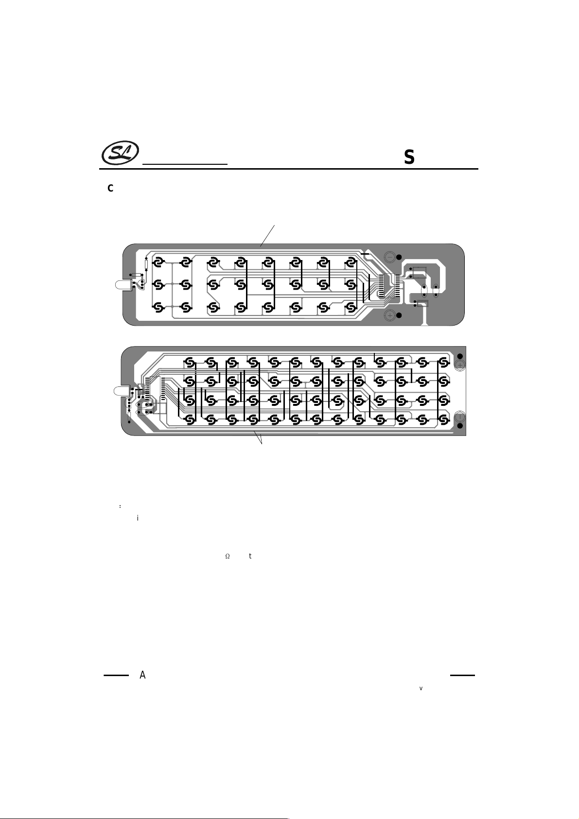
PCB WIRE LAYOUT SCHEMATIC:
SC6122
Transmitting tube output ground line
The transmitting tube ground line and IC ground line should
layout separated or overstriking ground line.
The above IC only use to hint, not to specified.
Note:
* In wire layout, the power filter capacitor should near to IC.
* In wire layout, should avoid power line and ground line too long.
* Recommended infrared transmit unit and IC ground line should layout separated, or overstriking lines.
* The emitter of triode connect 1
* Recommended triode use 9014.
resistor at least.
HANGZHOU SILAN MICROELECTRONICS JOINT-STOCK CO.,LTD
Rev: 2.2 2002-03-01
11
Page 12
Silan
Semiconductors
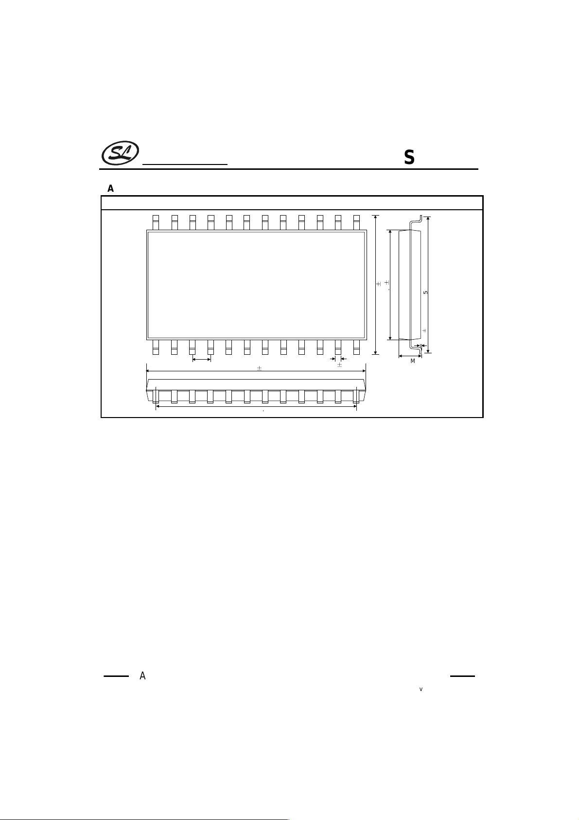
PACKAGE OUTLINE
SOP-24-375-1.27 Unit: mm
SC6122
0.3
0.4
B
B
7.6
10.2
9.525(375)
0.05
B
0.25
1.27
15.34B0.25
13.97
0.40
B
0.1
3.10MAX
HANGZHOU SILAN MICROELECTRONICS JOINT-STOCK CO.,LTD
Rev: 2.2 2002-03-01
12
Page 13

Silan
Attach
Semiconductors
SC6122
Revision History
Data REV Description Page
2000.12.31 2.0 Change name of company in page footer
2001.12.12 2.1
Modify the “Typical application circuit”
2002.03.01 2.2
Add the “PCB wire layout schematic”
Modify the “Package outline”
9
11
12
HANGZHOU SILAN MICROELECTRONICS JOINT-STOCK CO.,LTD
Rev: 2.2 2002-03-01
13
 Loading...