

Page 1

INTEGRATED CURCUITS
DATA SH EET
SC4000
Universal Timeslot Interchange
Preliminary specification
File under Integrated Curcuits
2000 Sep 07
Page 2

Philips Semiconductors Preliminary specification
Universal Timeslot Interchange SC4000
Features . . . . . . . . . . . . . . . . . . . . . . . . . . . . . . . . . . . . . . . . . . . . . . . . . . . . . . . . . . . . . . . . . . . . . . . . . . . . . . . . . . . . . . . . . . . . . . . . . . . . . . . . . . .1
Applications . . . . . . . . . . . . . . . . . . . . . . . . . . . . . . . . . . . . . . . . . . . . . . . . . . . . . . . . . . . . . . . . . . . . . . . . . . . . . . . . . . . . . . . . . . . . . . . . . . . . . . .1
Logic Pin Organization . . . . . . . . . . . . . . . . . . . . . . . . . . . . . . . . . . . . . . . . . . . . . . . . . . . . . . . . . . . . . . . . . . . . . . . . . . . . . . . . . . . . . . . . . . . . . . . .1
Block Diagram . . . . . . . . . . . . . . . . . . . . . . . . . . . . . . . . . . . . . . . . . . . . . . . . . . . . . . . . . . . . . . . . . . . . . . . . . . . . . . . . . . . . . . . . . . . . . . . . . . . . . .2
SC4000 100-Pin TQFP (top view) . . . . . . . . . . . . . . . . . . . . . . . . . . . . . . . . . . . . . . . . . . . . . . . . . . . . . . . . . . . . . . . . . . . . . . . . . . . . . . . . . . . . . . .2
SC4000 Physical Dimensions (all dimensions in millimeters) . . . . . . . . . . . . . . . . . . . . . . . . . . . . . . . . . . . . . . . . . . . . . . . . . . . . . . . . . . . . . . . . . .3
Pin Description . . . . . . . . . . . . . . . . . . . . . . . . . . . . . . . . . . . . . . . . . . . . . . . . . . . . . . . . . . . . . . . . . . . . . . . . . . . . . . . . . . . . . . . . . . . . . . . . . . . .4
Device Overview . . . . . . . . . . . . . . . . . . . . . . . . . . . . . . . . . . . . . . . . . . . . . . . . . . . . . . . . . . . . . . . . . . . . . . . . . . . . . . . . . . . . . . . . . . . . . . . . . . .6
Function Description . . . . . . . . . . . . . . . . . . . . . . . . . . . . . . . . . . . . . . . . . . . . . . . . . . . . . . . . . . . . . . . . . . . . . . . . . . . . . . . . . . . . . . . . . . . . . . .8
Switching . . . . . . . . . . . . . . . . . . . . . . . . . . . . . . . . . . . . . . . . . . . . . . . . . . . . . . . . . . . . . . . . . . . . . . . . . . . . . . . . . . . . . . . . . . . . . . . . . . . . . . . . . .8
PLL Timing and Clock Control . . . . . . . . . . . . . . . . . . . . . . . . . . . . . . . . . . . . . . . . . . . . . . . . . . . . . . . . . . . . . . . . . . . . . . . . . . . . . . . . . . . . . . . . . .8
Interrupts Control . . . . . . . . . . . . . . . . . . . . . . . . . . . . . . . . . . . . . . . . . . . . . . . . . . . . . . . . . . . . . . . . . . . . . . . . . . . . . . . . . . . . . . . . . . . . . . . . . . . .9
CLKFAIL Timing and Control . . . . . . . . . . . . . . . . . . . . . . . . . . . . . . . . . . . . . . . . . . . . . . . . . . . . . . . . . . . . . . . . . . . . . . . . . . . . . . . . . . . . . . . . . .11
Message Channel Interface . . . . . . . . . . . . . . . . . . . . . . . . . . . . . . . . . . . . . . . . . . . . . . . . . . . . . . . . . . . . . . . . . . . . . . . . . . . . . . . . . . . . . . . . . . .11
Operation Mode and Configuration Register Setup . . . . . . . . . . . . . . . . . . . . . . . . . . . . . . . . . . . . . . . . . . . . . . . . . . . . . . . . . . . . . . . . . . . . . . . . .11
Register Access Schemes . . . . . . . . . . . . . . . . . . . . . . . . . . . . . . . . . . . . . . . . . . . . . . . . . . . . . . . . . . . . . . . . . . . . . . . . . . . . . . . . . . . . . . . . . . . .16
Microprocessor Interface . . . . . . . . . . . . . . . . . . . . . . . . . . . . . . . . . . . . . . . . . . . . . . . . . . . . . . . . . . . . . . . . . . . . . . . . . . . . . . . . . . . . . . . . .17
I/O Address Map . . . . . . . . . . . . . . . . . . . . . . . . . . . . . . . . . . . . . . . . . . . . . . . . . . . . . . . . . . . . . . . . . . . . . . . . . . . . . . . . . . . . . . . . . . . . . . . . . . .17
Busy (D_0) (Read Only) . . . . . . . . . . . . . . . . . . . . . . . . . . . . . . . . . . . . . . . . . . . . . . . . . . . . . . . . . . . . . . . . . . . . . . . . . . . . . . . . . . . . . . . . . . . . . .17
Read (D_1) (Write only) . . . . . . . . . . . . . . . . . . . . . . . . . . . . . . . . . . . . . . . . . . . . . . . . . . . . . . . . . . . . . . . . . . . . . . . . . . . . . . . . . . . . . . . . . . . . . .17
Write (D_2) (Write only) . . . . . . . . . . . . . . . . . . . . . . . . . . . . . . . . . . . . . . . . . . . . . . . . . . . . . . . . . . . . . . . . . . . . . . . . . . . . . . . . . . . . . . . . . . . . .17
Terminate (D_3) (Read/Write) . . . . . . . . . . . . . . . . . . . . . . . . . . . . . . . . . . . . . . . . . . . . . . . . . . . . . . . . . . . . . . . . . . . . . . . . . . . . . . . . . . . . . . . . .17
Channel Bank Select Register [1:0] (D_[5:4]) (Read/Write) . . . . . . . . . . . . . . . . . . . . . . . . . . . . . . . . . . . . . . . . . . . . . . . . . . . . . . . . . . . . . . . . . . .17
Channel Bank Select Register Enable (D_6) (Write only) . . . . . . . . . . . . . . . . . . . . . . . . . . . . . . . . . . . . . . . . . . . . . . . . . . . . . . . . . . . . . . . . . . . . .17
Reset (D_7) (Read/Write) . . . . . . . . . . . . . . . . . . . . . . . . . . . . . . . . . . . . . . . . . . . . . . . . . . . . . . . . . . . . . . . . . . . . . . . . . . . . . . . . . . . . . . . . . . . . .18
Channel Specific Registers . . . . . . . . . . . . . . . . . . . . . . . . . . . . . . . . . . . . . . . . . . . . . . . . . . . . . . . . . . . . . . . . . . . . . . . . . . . . . . . . . . . . . . . . . . .19
Time-Slot Select [6:0] (Read/write) . . . . . . . . . . . . . . . . . . . . . . . . . . . . . . . . . . . . . . . . . . . . . . . . . . . . . . . . . . . . . . . . . . . . . . . . . . . . . . . . . . . . .20
Port Select [3:0] (Read/Write) . . . . . . . . . . . . . . . . . . . . . . . . . . . . . . . . . . . . . . . . . . . . . . . . . . . . . . . . . . . . . . . . . . . . . . . . . . . . . . . . . . . . . . . . .20
Parallel Access Enable (Read/Write) . . . . . . . . . . . . . . . . . . . . . . . . . . . . . . . . . . . . . . . . . . . . . . . . . . . . . . . . . . . . . . . . . . . . . . . . . . . . . . . . . . . .20
Switch Output Enable (Read/Write) . . . . . . . . . . . . . . . . . . . . . . . . . . . . . . . . . . . . . . . . . . . . . . . . . . . . . . . . . . . . . . . . . . . . . . . . . . . . . . . . . . . . .20
Time-Slot/Channel Select [6:0] (Read/Write) . . . . . . . . . . . . . . . . . . . . . . . . . . . . . . . . . . . . . . . . . . . . . . . . . . . . . . . . . . . . . . . . . . . . . . . . . . . . . .20
Port Select [3:0] (Read/Write) . . . . . . . . . . . . . . . . . . . . . . . . . . . . . . . . . . . . . . . . . . . . . . . . . . . . . . . . . . . . . . . . . . . . . . . . . . . . . . . . . . . . . . . . .20
Local Connect Enable (Read/Write) . . . . . . . . . . . . . . . . . . . . . . . . . . . . . . . . . . . . . . . . . . . . . . . . . . . . . . . . . . . . . . . . . . . . . . . . . . . . . . . . . . . . .20
Switch Output Enable (Read/Write) . . . . . . . . . . . . . . . . . . . . . . . . . . . . . . . . . . . . . . . . . . . . . . . . . . . . . . . . . . . . . . . . . . . . . . . . . . . . . . . . . . . . .20
Parallel Access . . . . . . . . . . . . . . . . . . . . . . . . . . . . . . . . . . . . . . . . . . . . . . . . . . . . . . . . . . . . . . . . . . . . . . . . . . . . . . . . . . . . . . . . . . . . . . . . . . . . .20
Serial Data [1:8] (Read/Write) . . . . . . . . . . . . . . . . . . . . . . . . . . . . . . . . . . . . . . . . . . . . . . . . . . . . . . . . . . . . . . . . . . . . . . . . . . . . . . . . . . . . . . . . .20
Source Parallel Access . . . . . . . . . . . . . . . . . . . . . . . . . . . . . . . . . . . . . . . . . . . . . . . . . . . . . . . . . . . . . . . . . . . . . . . . . . . . . . . . . . . . . . . . . . . . . . .20
Serial Data [1:8] (Read Only) . . . . . . . . . . . . . . . . . . . . . . . . . . . . . . . . . . . . . . . . . . . . . . . . . . . . . . . . . . . . . . . . . . . . . . . . . . . . . . . . . . . . . . . . . .20
2000 Sep 07 2
Page 3

Philips Semiconductors Preliminary specification
Universal Timeslot Interchange SC4000
Configuration Registers . . . . . . . . . . . . . . . . . . . . . . . . . . . . . . . . . . . . . . . . . . . . . . . . . . . . . . . . . . . . . . . . . . . . . . . . . . . . . . . . . . . . . . . . . . .21
SCbus Clock Master (C_0) (Read/Write) . . . . . . . . . . . . . . . . . . . . . . . . . . . . . . . . . . . . . . . . . . . . . . . . . . . . . . . . . . . . . . . . . . . . . . . . . . . . . . . . .21
SCbus Clock Master Arm (C_1) (Read/Write) . . . . . . . . . . . . . . . . . . . . . . . . . . . . . . . . . . . . . . . . . . . . . . . . . . . . . . . . . . . . . . . . . . . . . . . . . . . . .21
SCbus Primary/Alternate Select (C_2) (Read/Write) . . . . . . . . . . . . . . . . . . . . . . . . . . . . . . . . . . . . . . . . . . . . . . . . . . . . . . . . . . . . . . . . . . . . . . . .21
Diagnostic Mode Enable (C_3) (Read/Write) . . . . . . . . . . . . . . . . . . . . . . . . . . . . . . . . . . . . . . . . . . . . . . . . . . . . . . . . . . . . . . . . . . . . . . . . . . . . . .21
SCbus Framing Mode [1:0](C_[5:4]) (Read/Write) . . . . . . . . . . . . . . . . . . . . . . . . . . . . . . . . . . . . . . . . . . . . . . . . . . . . . . . . . . . . . . . . . . . . . . . . .21
Local bus Framing Mode [1:0](C_[7:6]) (Read/Write) . . . . . . . . . . . . . . . . . . . . . . . . . . . . . . . . . . . . . . . . . . . . . . . . . . . . . . . . . . . . . . . . . . . . . . .21
Master Clock Input Frequency Select [2:0] (C_[10:8]) (Read/Write) . . . . . . . . . . . . . . . . . . . . . . . . . . . . . . . . . . . . . . . . . . . . . . . . . . . . . . . . . . . .21
Direct R/W to Parallel Access Registers Enable (C_11) (Read/Write) . . . . . . . . . . . . . . . . . . . . . . . . . . . . . . . . . . . . . . . . . . . . . . . . . . . . . . . . . . . .21
Message Channel Registered TXD Enable (C_12) (Read/Write) . . . . . . . . . . . . . . . . . . . . . . . . . . . . . . . . . . . . . . . . . . . . . . . . . . . . . . . . . . . . . . . .21
Message Channel TXD_0 or TXD_1 Select (C_13) (Read/Write) . . . . . . . . . . . . . . . . . . . . . . . . . . . . . . . . . . . . . . . . . . . . . . . . . . . . . . . . . . . . . . .22
Message Channel Clock Duty Cycle Select (C_14) (Read/Write) . . . . . . . . . . . . . . . . . . . . . . . . . . . . . . . . . . . . . . . . . . . . . . . . . . . . . . . . . . . . . . .22
Message Channel Output Disable (W/ loopback) (C_15) (Read/Write) . . . . . . . . . . . . . . . . . . . . . . . . . . . . . . . . . . . . . . . . . . . . . . . . . . . . . . . . . .22
SCbus SD Sample Position (C_16) (Read/Write) . . . . . . . . . . . . . . . . . . . . . . . . . . . . . . . . . . . . . . . . . . . . . . . . . . . . . . . . . . . . . . . . . . . . . . . . . .22
Local Bus SI Sample Position (C_17) (Read/Write) . . . . . . . . . . . . . . . . . . . . . . . . . . . . . . . . . . . . . . . . . . . . . . . . . . . . . . . . . . . . . . . . . . . . . . . . .22
SCbus SD Output Delay Enable (C_18) (Read/Write) . . . . . . . . . . . . . . . . . . . . . . . . . . . . . . . . . . . . . . . . . . . . . . . . . . . . . . . . . . . . . . . . . . . . . . .22
Local bus SO Output Delay Enable (C_19) (Read/Write) . . . . . . . . . . . . . . . . . . . . . . . . . . . . . . . . . . . . . . . . . . . . . . . . . . . . . . . . . . . . . . . . . . . . .22
SCbus FSYNCN Sample Position (C_20) (Read/Write) . . . . . . . . . . . . . . . . . . . . . . . . . . . . . . . . . . . . . . . . . . . . . . . . . . . . . . . . . . . . . . . . . . . . . .22
SCbus FSYNCN Rate (C_21) (Read/Write) . . . . . . . . . . . . . . . . . . . . . . . . . . . . . . . . . . . . . . . . . . . . . . . . . . . . . . . . . . . . . . . . . . . . . . . . . . . . . . .22
SCbus SCLKX2N, SCLKX2NA Output Disable(C_22) (Read/Write) . . . . . . . . . . . . . . . . . . . . . . . . . . . . . . . . . . . . . . . . . . . . . . . . . . . . . . . . . . . . .22
SCbus Alternate (“A”) Signals Output Enable (C_23) (Read/Write) . . . . . . . . . . . . . . . . . . . . . . . . . . . . . . . . . . . . . . . . . . . . . . . . . . . . . . . . . . . . .23
Local bus L_CLK Polarity (C_24) (Read/Write) . . . . . . . . . . . . . . . . . . . . . . . . . . . . . . . . . . . . . . . . . . . . . . . . . . . . . . . . . . . . . . . . . . . . . . . . . . . .23
Local bus L_FS Polarity (C_25) (Read/Write) . . . . . . . . . . . . . . . . . . . . . . . . . . . . . . . . . . . . . . . . . . . . . . . . . . . . . . . . . . . . . . . . . . . . . . . . . . . . .23
Local bus L_FS Position (C_[27:26]) (Read/Write) . . . . . . . . . . . . . . . . . . . . . . . . . . . . . . . . . . . . . . . . . . . . . . . . . . . . . . . . . . . . . . . . . . . . . . . . .23
Local bus L_CLK & L_FS Rate (C_28) (Read/Write) . . . . . . . . . . . . . . . . . . . . . . . . . . . . . . . . . . . . . . . . . . . . . . . . . . . . . . . . . . . . . . . . . . . . . . . .23
Local bus L_CLK DPLL Enable (C_29) (Read/Write) . . . . . . . . . . . . . . . . . . . . . . . . . . . . . . . . . . . . . . . . . . . . . . . . . . . . . . . . . . . . . . . . . . . . . . . .23
Local bus L_CLK 8.192 MHz 62.5% Duty Cycle (C_30) (Read/Write) . . . . . . . . . . . . . . . . . . . . . . . . . . . . . . . . . . . . . . . . . . . . . . . . . . . . . . . . . .23
Version/Revision Status (C_[39:32]) . . . . . . . . . . . . . . . . . . . . . . . . . . . . . . . . . . . . . . . . . . . . . . . . . . . . . . . . . . . . . . . . . . . . . . . . . . . . . . . . . . . .23
Master PLL Reference Select [2:0] (C_[42:40]) (Read/Write) . . . . . . . . . . . . . . . . . . . . . . . . . . . . . . . . . . . . . . . . . . . . . . . . . . . . . . . . . . . . . . . . . .23
Internal/External Master PLL Select (C_43) (Read/Write) . . . . . . . . . . . . . . . . . . . . . . . . . . . . . . . . . . . . . . . . . . . . . . . . . . . . . . . . . . . . . . . . . . . .24
SCbus SREF_8K Source Select [1:0] (C_[45:44]) (Read/Write) . . . . . . . . . . . . . . . . . . . . . . . . . . . . . . . . . . . . . . . . . . . . . . . . . . . . . . . . . . . . . . .24
SCbus SREF_8K Output Enable (C_46) (Read/Write) . . . . . . . . . . . . . . . . . . . . . . . . . . . . . . . . . . . . . . . . . . . . . . . . . . . . . . . . . . . . . . . . . . . . . . .24
SCbus SCLK 8.192 MHz 62.5% Duty Cycle (C_47) (Read/Write) . . . . . . . . . . . . . . . . . . . . . . . . . . . . . . . . . . . . . . . . . . . . . . . . . . . . . . . . . . . . . .24
Clock Watchdog Enable (C_48) (Read/Write) . . . . . . . . . . . . . . . . . . . . . . . . . . . . . . . . . . . . . . . . . . . . . . . . . . . . . . . . . . . . . . . . . . . . . . . . . . . . .24
Microprocessor Watchdog Enable (C_49) (Read/Write) . . . . . . . . . . . . . . . . . . . . . . . . . . . . . . . . . . . . . . . . . . . . . . . . . . . . . . . . . . . . . . . . . . . . .24
SCbus CLKFAIL Latch Set Polarity Select (C_50) (Read/Write) . . . . . . . . . . . . . . . . . . . . . . . . . . . . . . . . . . . . . . . . . . . . . . . . . . . . . . . . . . . . . . . .24
SCbus CLKFAIL Latch Debounce Enable (C_51) (Read/Write) . . . . . . . . . . . . . . . . . . . . . . . . . . . . . . . . . . . . . . . . . . . . . . . . . . . . . . . . . . . . . . . .24
Frame Boundary Latch Set Delay Enable (C_52) (Read/Write) . . . . . . . . . . . . . . . . . . . . . . . . . . . . . . . . . . . . . . . . . . . . . . . . . . . . . . . . . . . . . . . . .25
INT_0 Mask_N (C_53) (Read/Write) . . . . . . . . . . . . . . . . . . . . . . . . . . . . . . . . . . . . . . . . . . . . . . . . . . . . . . . . . . . . . . . . . . . . . . . . . . . . . . . . . . . .25
INT_0 Output Polarity (C_54) (Read/Write) . . . . . . . . . . . . . . . . . . . . . . . . . . . . . . . . . . . . . . . . . . . . . . . . . . . . . . . . . . . . . . . . . . . . . . . . . . . . . . .25
INT_0 Output Driver (C_55) (Read/Write) . . . . . . . . . . . . . . . . . . . . . . . . . . . . . . . . . . . . . . . . . . . . . . . . . . . . . . . . . . . . . . . . . . . . . . . . . . . . . . . .25
SCbus CLKFAIL Latch (C_56) (Read Only) . . . . . . . . . . . . . . . . . . . . . . . . . . . . . . . . . . . . . . . . . . . . . . . . . . . . . . . . . . . . . . . . . . . . . . . . . . . . . . .25
Frame Boundary Latch (C_57) (Read only) . . . . . . . . . . . . . . . . . . . . . . . . . . . . . . . . . . . . . . . . . . . . . . . . . . . . . . . . . . . . . . . . . . . . . . . . . . . . . . .25
2000 Sep 07 3
Page 4

Philips Semiconductors Preliminary specification
Universal Timeslot Interchange SC4000
Internal Master PLL Error Latch (C_58) (Read Only) . . . . . . . . . . . . . . . . . . . . . . . . . . . . . . . . . . . . . . . . . . . . . . . . . . . . . . . . . . . . . . . . . . . . . . . .25
SCbus Error Indicator (C_59) (Read Only) . . . . . . . . . . . . . . . . . . . . . . . . . . . . . . . . . . . . . . . . . . . . . . . . . . . . . . . . . . . . . . . . . . . . . . . . . . . . . . . .25
SCbus CLKFAIL Latch Clear_N (C_60) (Read/Write) . . . . . . . . . . . . . . . . . . . . . . . . . . . . . . . . . . . . . . . . . . . . . . . . . . . . . . . . . . . . . . . . . . . . . . .25
Frame Boundary Latch Clear_N (C_61) (Read/Write) . . . . . . . . . . . . . . . . . . . . . . . . . . . . . . . . . . . . . . . . . . . . . . . . . . . . . . . . . . . . . . . . . . . . . . .25
Internal Master PLL Error Latch Clear_N (C_62) (Read/Write) . . . . . . . . . . . . . . . . . . . . . . . . . . . . . . . . . . . . . . . . . . . . . . . . . . . . . . . . . . . . . . . .25
SCbus SCLKX2N Error Latch (C_64) (Read Only) . . . . . . . . . . . . . . . . . . . . . . . . . . . . . . . . . . . . . . . . . . . . . . . . . . . . . . . . . . . . . . . . . . . . . . . . . .25
SCbus SCLKX2NA Error Latch (C_65) (Read only) . . . . . . . . . . . . . . . . . . . . . . . . . . . . . . . . . . . . . . . . . . . . . . . . . . . . . . . . . . . . . . . . . . . . . . . . .26
SCbus SCLK Error Latch (C_66) (Read only) . . . . . . . . . . . . . . . . . . . . . . . . . . . . . . . . . . . . . . . . . . . . . . . . . . . . . . . . . . . . . . . . . . . . . . . . . . . . .26
SCbus SCLKA Error Latch (C_67) (Read only) . . . . . . . . . . . . . . . . . . . . . . . . . . . . . . . . . . . . . . . . . . . . . . . . . . . . . . . . . . . . . . . . . . . . . . . . . . . .26
SCbus SCLKX2N Error Latch Clear_N (C_68) (Read/Write) . . . . . . . . . . . . . . . . . . . . . . . . . . . . . . . . . . . . . . . . . . . . . . . . . . . . . . . . . . . . . . . . . .26
SCbus SCLKX2NA Error Latch Clear_N (C_69) (Read/Write) . . . . . . . . . . . . . . . . . . . . . . . . . . . . . . . . . . . . . . . . . . . . . . . . . . . . . . . . . . . . . . . . .26
SCbus SCLK Error Latch Clear_N (C_70) (Read/Write) . . . . . . . . . . . . . . . . . . . . . . . . . . . . . . . . . . . . . . . . . . . . . . . . . . . . . . . . . . . . . . . . . . . . . .26
SCbus SCLKA Error Latch Clear_N(C_71) (Read/Write) . . . . . . . . . . . . . . . . . . . . . . . . . . . . . . . . . . . . . . . . . . . . . . . . . . . . . . . . . . . . . . . . . . . . .26
SCbus FSYNCN Error Latch (C_72) (Read Only) . . . . . . . . . . . . . . . . . . . . . . . . . . . . . . . . . . . . . . . . . . . . . . . . . . . . . . . . . . . . . . . . . . . . . . . . . . .26
SCbus FSYNCNA Error Latch (C_73) (Read Only) . . . . . . . . . . . . . . . . . . . . . . . . . . . . . . . . . . . . . . . . . . . . . . . . . . . . . . . . . . . . . . . . . . . . . . . . . .26
SCbus Clock Master Error Latch (C_74) (Read Only) . . . . . . . . . . . . . . . . . . . . . . . . . . . . . . . . . . . . . . . . . . . . . . . . . . . . . . . . . . . . . . . . . . . . . . .26
SCbus FSYNCN Error Latch Clear_N (C_76) (Read/Write) . . . . . . . . . . . . . . . . . . . . . . . . . . . . . . . . . . . . . . . . . . . . . . . . . . . . . . . . . . . . . . . . . . .26
SCbus FSYNCNA Error Latch Clear_N (C_77) (Read/Write) . . . . . . . . . . . . . . . . . . . . . . . . . . . . . . . . . . . . . . . . . . . . . . . . . . . . . . . . . . . . . . . . . .26
SCbus Clock Master Error Latch Clear_N (C_78) (Read/Write) . . . . . . . . . . . . . . . . . . . . . . . . . . . . . . . . . . . . . . . . . . . . . . . . . . . . . . . . . . . . . . . .26
SCbus SREF_8K NE SREF_8KA Error Latch (C_80) (Read only) . . . . . . . . . . . . . . . . . . . . . . . . . . . . . . . . . . . . . . . . . . . . . . . . . . . . . . . . . . . . . . .27
SCbus CLKFAIL NE CLKFAILA Error Latch (C_81) (Read only) . . . . . . . . . . . . . . . . . . . . . . . . . . . . . . . . . . . . . . . . . . . . . . . . . . . . . . . . . . . . . . . .27
SCbus MC NE MCA Error Latch (C_82) (Read only) . . . . . . . . . . . . . . . . . . . . . . . . . . . . . . . . . . . . . . . . . . . . . . . . . . . . . . . . . . . . . . . . . . . . . . . .27
SCbus SD Error Indicator (C_83) (Read only) . . . . . . . . . . . . . . . . . . . . . . . . . . . . . . . . . . . . . . . . . . . . . . . . . . . . . . . . . . . . . . . . . . . . . . . . . . . . .27
SCbus SREF_8K NE SREF_8KA Error Latch Clear_N (C_84) (Read/Write) . . . . . . . . . . . . . . . . . . . . . . . . . . . . . . . . . . . . . . . . . . . . . . . . . . . . . . .27
SCbus CLKFAIL NE CLKFAILA Error Latch Clear_N (C_85) (Read/write) . . . . . . . . . . . . . . . . . . . . . . . . . . . . . . . . . . . . . . . . . . . . . . . . . . . . . . . .27
SCbus MC NE MCA Error Latch Clear_N (C_86) (Read/Write) . . . . . . . . . . . . . . . . . . . . . . . . . . . . . . . . . . . . . . . . . . . . . . . . . . . . . . . . . . . . . . . .27
SCbus SD Error Latch Clear_N (C_87) (Read/Write) . . . . . . . . . . . . . . . . . . . . . . . . . . . . . . . . . . . . . . . . . . . . . . . . . . . . . . . . . . . . . . . . . . . . . . . .27
SCbus SD_[15:0] Error Latch (C_[103:88]) (Read only) . . . . . . . . . . . . . . . . . . . . . . . . . . . . . . . . . . . . . . . . . . . . . . . . . . . . . . . . . . . . . . . . . . . . .27
Summary of SC4000 Configuration Registers . . . . . . . . . . . . . . . . . . . . . . . . . . . . . . . . . . . . . . . . . . . . . . . . . . . . . . . . . . . . . . . . . . . . . .27
Miscellaneous . . . . . . . . . . . . . . . . . . . . . . . . . . . . . . . . . . . . . . . . . . . . . . . . . . . . . . . . . . . . . . . . . . . . . . . . . . . . . . . . . . . . . . . . . . . . . . . . . . . . .27
Master Clock/PLL . . . . . . . . . . . . . . . . . . . . . . . . . . . . . . . . . . . . . . . . . . . . . . . . . . . . . . . . . . . . . . . . . . . . . . . . . . . . . . . . . . . . . . . . . . . . . . . . . .27
SCbus (MVIP Bus) . . . . . . . . . . . . . . . . . . . . . . . . . . . . . . . . . . . . . . . . . . . . . . . . . . . . . . . . . . . . . . . . . . . . . . . . . . . . . . . . . . . . . . . . . . . . . . . . . .27
Local Bus . . . . . . . . . . . . . . . . . . . . . . . . . . . . . . . . . . . . . . . . . . . . . . . . . . . . . . . . . . . . . . . . . . . . . . . . . . . . . . . . . . . . . . . . . . . . . . . . . . . . . . . . .28
Message Channel . . . . . . . . . . . . . . . . . . . . . . . . . . . . . . . . . . . . . . . . . . . . . . . . . . . . . . . . . . . . . . . . . . . . . . . . . . . . . . . . . . . . . . . . . . . . . . . . . .28
Watchdog . . . . . . . . . . . . . . . . . . . . . . . . . . . . . . . . . . . . . . . . . . . . . . . . . . . . . . . . . . . . . . . . . . . . . . . . . . . . . . . . . . . . . . . . . . . . . . . . . . . . . . . . .28
Interrupt . . . . . . . . . . . . . . . . . . . . . . . . . . . . . . . . . . . . . . . . . . . . . . . . . . . . . . . . . . . . . . . . . . . . . . . . . . . . . . . . . . . . . . . . . . . . . . . . . . . . . . . . . .28
Reserved Bit . . . . . . . . . . . . . . . . . . . . . . . . . . . . . . . . . . . . . . . . . . . . . . . . . . . . . . . . . . . . . . . . . . . . . . . . . . . . . . . . . . . . . . . . . . . . . . . . . . . . . . .28
Typical Internal Register Access . . . . . . . . . . . . . . . . . . . . . . . . . . . . . . . . . . . . . . . . . . . . . . . . . . . . . . . . . . . . . . . . . . . . . . . . . . . . . . . . . .28
Typical Write Internal Register Access . . . . . . . . . . . . . . . . . . . . . . . . . . . . . . . . . . . . . . . . . . . . . . . . . . . . . . . . . . . . . . . . . . . . . . . . . . . . . . . . . . .28
Typical Read Internal Register Access . . . . . . . . . . . . . . . . . . . . . . . . . . . . . . . . . . . . . . . . . . . . . . . . . . . . . . . . . . . . . . . . . . . . . . . . . . . . . . . . . . .28
Test . . . . . . . . . . . . . . . . . . . . . . . . . . . . . . . . . . . . . . . . . . . . . . . . . . . . . . . . . . . . . . . . . . . . . . . . . . . . . . . . . . . . . . . . . . . . . . . . . . . . . . . . . . . . .29
Electrical Specifications . . . . . . . . . . . . . . . . . . . . . . . . . . . . . . . . . . . . . . . . . . . . . . . . . . . . . . . . . . . . . . . . . . . . . . . . . . . . . . . . . . . . . . . . . .30
AC Electrical Characteristics . . . . . . . . . . . . . . . . . . . . . . . . . . . . . . . . . . . . . . . . . . . . . . . . . . . . . . . . . . . . . . . . . . . . . . . . . . . . . . . . . . . . . .31
2000 Sep 07 4
Page 5

Philips Semiconductors Preliminary specification
Universal Timeslot Interchange SC4000
Table 1. Configuration Register Setup for SCbus Clock Slave . . . . . . . . . . . . . . . . . . . . . . . . . . . . . . . . . . . . . . . . . . . . . . . . . . . . . .11
Table 2. Configuration Register Setup for SCbus Clock Master. . . . . . . . . . . . . . . . . . . . . . . . . . . . . . . . . . . . . . . . . . . . . . . . . . . . . 12
Table 3. Configuration Register Setup for SCbus Armed Clock Master. . . . . . . . . . . . . . . . . . . . . . . . . . . . . . . . . . . . . . . . . . . . . . . 13
Table 4. Configuration Register Setup for MVIP Clock Master . . . . . . . . . . . . . . . . . . . . . . . . . . . . . . . . . . . . . . . . . . . . . . . . . . . . . 14
Table 5. Configuration Register Setup for MVIP Clock Slave. . . . . . . . . . . . . . . . . . . . . . . . . . . . . . . . . . . . . . . . . . . . . . . . . . . . . . . 14
Table 6. SCbus/MVIP Signals Cross Reference. . . . . . . . . . . . . . . . . . . . . . . . . . . . . . . . . . . . . . . . . . . . . . . . . . . . . . . . . . . . . . . . . 15
Table 7. Microprocessor Interface Timing - Intel Bus Mode . . . . . . . . . . . . . . . . . . . . . . . . . . . . . . . . . . . . . . . . . . . . . . . . . . . . . . . 31
Table 8. Microprocessor Interface Timing - Intel Bus Mode . . . . . . . . . . . . . . . . . . . . . . . . . . . . . . . . . . . . . . . . . . . . . . . . . . . . . . . 32
Table 9. Microprocessor Interface Timing - Multiplexed Address . . . . . . . . . . . . . . . . . . . . . . . . . . . . . . . . . . . . . . . . . . . . . . . . . . . 33
Table 10. Local Bus Timing, 1X L_CLK Mode (C_28=0) . . . . . . . . . . . . . . . . . . . . . . . . . . . . . . . . . . . . . . . . . . . . . . . . . . . . . . . . . . . 34
Table 11. Local Bus Timing, 2X L_CLK Mode (C_28=1) . . . . . . . . . . . . . . . . . . . . . . . . . . . . . . . . . . . . . . . . . . . . . . . . . . . . . . . . . . . 35
Table 12. SCbus Timing . . . . . . . . . . . . . . . . . . . . . . . . . . . . . . . . . . . . . . . . . . . . . . . . . . . . . . . . . . . . . . . . . . . . . . . . . . . . . . . . . . . .36
Table 13. SCbus Clock Master Timing . . . . . . . . . . . . . . . . . . . . . . . . . . . . . . . . . . . . . . . . . . . . . . . . . . . . . . . . . . . . . . . . . . . . . . . . . 38
Table 14. SCbus Clock Fail Timing . . . . . . . . . . . . . . . . . . . . . . . . . . . . . . . . . . . . . . . . . . . . . . . . . . . . . . . . . . . . . . . . . . . . . . . . . . . 39
Table 15. REF_8K_[3:0] and SREF_8K Timing . . . . . . . . . . . . . . . . . . . . . . . . . . . . . . . . . . . . . . . . . . . . . . . . . . . . . . . . . . . . . . . . . . 40
2000 Sep 07 5
Page 6

Philips Semiconductors Preliminary specification
Universal Timeslot Interchange SC4000
Figure 1.
Figure 2. Internal Master PLL (C_43 = 0) Function Block . . . . . . . . . . . . . . . . . . . . . . . . . . . . . . . . . . . . . . . . . . . . . . . . . . . . . . . . . . . . . . . . . . . . .8
Figure 3.
Figure 4. Internal PLL and Local Bus PLL Timing Function Block . . . . . . . . . . . . . . . . . . . . . . . . . . . . . . . . . . . . . . . . . . . . . . . . . . . . . . . . . . . . .10
Figure 5.
Figure 6.
Figure 7.
Figure 8.
Figure 9.
Figure 10.
Figure 11.
Figure 12.
Figure 13.
Figure 14.
Figure 15.
Destination and Source Switch Function Block . . . . . . . . . . . . . . . . . . . . . . . . . . . . . . . . . . . . . . . . . . . . . . . . . . . . . . . . . . . . . . . . . . . . .7
External Master PLL (C_43 = 1) Function Block . . . . . . . . . . . . . . . . . . . . . . . . . . . . . . . . . . . . . . . . . . . . . . . . . . . . . . . . . . . . . . . . . . . .9
Using Two Pins A_[1:0] for Address Bus Interface Scheme (C_11 = 0) . . . . . . . . . . . . . . . . . . . . . . . . . . . . . . . . . . . . . . . . . . . . . . . . .16
Using Nine Pins A_[8:0] for Address Bus Interface Scheme (C_11 = 1) . . . . . . . . . . . . . . . . . . . . . . . . . . . . . . . . . . . . . . . . . . . . . . . . .16
Microprocessor Interface Timing - Intel Bus Mode (Pin I_N = 0), Non-Multiplexed Address . . . . . . . . . . . . . . . . . . . . . . . . . . . . . . . . .31
Microprocessor Interface Timing - Motorola Bus Mode (Pin I_N = 1), Non-multiplexed Address . . . . . . . . . . . . . . . . . . . . . . . . . . . . . .32
Microprocessor Interface Timing - Multiplexed Address . . . . . . . . . . . . . . . . . . . . . . . . . . . . . . . . . . . . . . . . . . . . . . . . . . . . . . . . . . . . .33
Local Bus Timing, 1XL_CLK Mode (C_28=0) . . . . . . . . . . . . . . . . . . . . . . . . . . . . . . . . . . . . . . . . . . . . . . . . . . . . . . . . . . . . . . . . . . . . .34
Local Bus Timing, 2X L_CLK Mode (C_28=1) . . . . . . . . . . . . . . . . . . . . . . . . . . . . . . . . . . . . . . . . . . . . . . . . . . . . . . . . . . . . . . . . . . . .35
SCbus Timing . . . . . . . . . . . . . . . . . . . . . . . . . . . . . . . . . . . . . . . . . . . . . . . . . . . . . . . . . . . . . . . . . . . . . . . . . . . . . . . . . . . . . . . . . . . . .36
SCbus Clock Master Timing . . . . . . . . . . . . . . . . . . . . . . . . . . . . . . . . . . . . . . . . . . . . . . . . . . . . . . . . . . . . . . . . . . . . . . . . . . . . . . . . . .38
SCbus Clock Fail Timing . . . . . . . . . . . . . . . . . . . . . . . . . . . . . . . . . . . . . . . . . . . . . . . . . . . . . . . . . . . . . . . . . . . . . . . . . . . . . . . . . . . . .39
REF_8K_[3:0] and SREF_8K input mode Timing . . . . . . . . . . . . . . . . . . . . . . . . . . . . . . . . . . . . . . . . . . . . . . . . . . . . . . . . . . . . . . . . . .40
2000 Sep 07 6
Page 7

Philips Semiconductors Preliminary specification
Universal Timeslot Interchange SC4000
FEATURES
• Timeslot interchange between local
and expansion buses
• Architecture optimized for call processing environments: SCbus™,
MVIP® and ST-BUS Compatible
• Full switching between any of:
– 128 local bus input SI timeslots
– 128 local bus output SO timeslots
– up to 2048 expansion bus SD
timeslots
• Multiple local bus speeds and
formats:
– 2.048, 4.096 or 8.192 Mb/s
– PEB®, STbus or GCI
Logic Pin Organization
• Supports both Intel® and Motorola®
processor interfaces
• Serial or parallel access to expansion
bus
• Enhanced input hysteresis threshold
• Internal phased lock loop
• Fast response and support for SCbus
clock fallback
• Flexible local frame sync interface
• Supports hyper channel capability
(bundling)
• SCbus message bus interface and local
loopback control
• High availability and self-diagnostic
features
44
D_7
43
D_6
42
D_5
40
D_4
39
D_3
38
D_2
36
D_1
35
D_0
34
A_8
32
A_7
31
A_6
30
A_5
28
A_4
27
A_3
26
A_2
25
A_1
24
A_0
22
ALE
17
CS_1_N
16
CS_0_N
19
RD_N(STRB_N)
20
WR_N(R/W_N)
21
DACK_N
96
RESET
12
I_N(M)
2
X_IN
1
X_OUT
7
REF_8K_3(REF_8K_OUT)
6
REF_8K_2(CLK_IN)
5
REF_8K_1
4
REF_8K_0
95
SI_3
94
SI_2
92
SI_1
91
SI_0
9
TXD_0
98
TEST
(TEST_OUT_0)DRQ_R
(TEST_OUT_1)DRQ_T
SC4000
INT_1
INT_0
SCLKX2N
SCLKX2NA
SCLK
SCLKA
SREF_8K
SREF_8KA
FSYNCN
FSYNCNA
CLKFAIL
CLKFAILA
SD_0
SD_1
SD_2
SD_3
SD_4
SD_5
SD_6
SD_7
SD_8
SD_9
SD_10
SD_11
SD_12
SD_13
SD_14
SD_15
MC
MCA
L_CLK
L_FS
SO_3
SO_2
SO_1
SO_0
MC_CLK
RXD
• 5V CMOS technology
• 100-pin TQFP package
APPLICATIONS
• PC-based switching
• Small to medium size digital switch
matrices
• SCbus/MVIP interface functions
• Digital centralized voice processing
system
• Voice/Data multiplexer and exchange
• Computer telephony interface
15
14
99
100
46
47
49
50
51
52
54
55
56
58
59
60
62
63
64
66
67
68
70
71
72
74
75
76
77
79
80
81
83
84
90
88
87
86
11
10
2000 Sep 07 7
Page 8

Philips Semiconductors Preliminary specification
Universal Timeslot Interchange SC4000
Block Diagram
SI_[3:0]
SO_[3:0]
Local Bus Timing
CLK_IN
REF_8K_[3:0]
A_[8:0]
D_[7:0]
Control
SC4000 100-Pin TQFP (top view)
Micro
Processor
Interface
SD_12
SD_11
VSS
SD_10
SD_9
Control
Bus
SD_8
VSS
SD_7
SD_6
SD_5
Timing
DPLL
VDD
SD_4
SD_3
SD_2
VDD
SD_1
SD_0
128 x 2048
Destination
Switch
128 x 2176
Source
Switch
CLKFAILA
VSS
CLKFAIL
FSYNCNA
FSYNCN
VSS
SREF_8KA
SD_[15:0]
Local
Connect
SCbus Timing
SERF_8K
SD_13
SD_14
VDD
SD_15
MC
MCA
VSS
L_CLK
L_FS
VDD
SO_0
SO_1
SO_2
VDD
SO_3
SI_0
SI_1
VSS
SI_2
SI_3
RESET
VSS
TEST
DRQ_R
DRQ_T
75747372717069686766656463626160595857565554535251
76
77
78
79
80
81
82
83
84
85
86
87
88
89
90
91
92
93
94
95
96
97
98
99
100
1 2 3 4 5 6 7 8 9 10 11121314 15 16 17 1819 202122 23 24 25
VSS
X_IN
X_OUT
REF_8K_0
REF_8K_1
SC4000
100-PIN TQFP
(TOP VIEW)
I_N
VDD
RXD
VDD
INT_0
REF_8K_2
REF_8K_3
TXD_0
MC_CLK
INT_1
CS_0_N
VSS
SC_1_N
RD_N
WR_N
DACK_N
ALE
VSS
A_0
A_1
SCLKA
50
49
SCLK
48
VDD
SCLKX2NA
47
46
SCLKX2N
45
VSS
D_7
44
D_6
43
42
D_5
41
VSS
40
D_4
D_3
39
D_2
38
37
VDD
36
D_1
D_0
35
A_8
34
33
VSS
32
A_7
A_6
31
A_5
30
29
VDD
A_4
28
27
A_3
26
A_2
2000 Sep 07 8
Page 9

Philips Semiconductors Preliminary specification
Universal Timeslot Interchange SC4000
SC4000 Physical Dimensions (all dimensions in millimeters)
+
_
16.00 0.40
+
_
14.00 0.20
16.00 0.40
14.00 0.20
+
_
+
_
+
_
1.40 0.05
0.15
MAX
0.50
Typ
+
_
0.22 0.05
o
12 REF
o
12 REF
0.20
1.00 REF
0.14
0.25
00-
0.60
MIN
+
_
0.04
0
10
+
_
0.15
2000 Sep 07 9
Page 10
Philips Semiconductors Preliminary specification
Universal Timeslot Interchange SC4000
PIN DESCRIPTION
Pin Name Input/Output Pin Number Pin Description
D_[7:0] I/O 44,43,42,40,
A_[8:0] I 34,32,31,30,
ALE I 22 (TTL Input) Address Latch Enable. This input pin is tied to high in non-multiplexed mode. Otherwise, in multi-
CS_1_N I 17 (TTL Input) Chip Select 1. Reserved for future internal HDLC controller. If unused, this pin should be connected to
CS_0_N I 16 (TTL Input) Chip Select 0. This active low signal selects the SC4000
I_N
or
M
RD_N
or
STRB_N
WR_N
or
R/W_N
DACK_N I 21 (TTL Input, Pull up) DMA Acknowledge Reserved for future internal HDLC controller. If unused, this pin should be
RESET I 96 (TTL Input) Reset. This active high signal initializes the microprocessor interface, configuration, routing and paral-
X_IN I 2 (CMOS Input) Crystal Clock Input. This pin is a CMOS level input of either 2.048, 4.096, 8.192, 16.384, 32.768 or
X_OUT O 1 (CMOS Output) Crystal Clock Output.
REF_8K_3
or
REF_8K_OUT
REF_8K_2
or
CLK_IN
REF_8K_1 I 5 (TTL Input) Local 8 KHz Reference 1 Input.
I 12 (TTL Input) Microprocessor Bus Interface Mode Select.
I 19 (TTL Input) In Intel Bus Mode (RD_N), this active low input operates with CS_0_N to configure the data bus lines
I 20 (TTL Input) In Intel Bus Mode (WR_N), when CS_0_N is active, the rising edge of WR_N is used to latch an inter-
I
O
I 6 (TTL Input) Internal Master PLL (REF_8K_2). If configuration register bit C_43=0, this pin is a Local 8 KHz Refer-
39,38,36,35
28,27,26,25,24
7 (TTL Bi-Directional) Internal Master PLL (REF_8K_3). If configuration register bit C_43=0, this pin is a Local 8
(TTL Bi-directional) Microprocessor Data Bus. These bi-directional, tri-state lines allow the microprocessor to
access SC4000 internal registers as well as the source/destination routing memory and parallel access registers.
(TTL Input) Microprocessor Address Bus. These inputs select the internal registers used by a read or write operation. Normally these inputs are connected to Microprocessor address lines A[8:0].
plexed mode, the Microprocessor Address Bus is latched internally on the falling edge of this signal.
high.
for a microprocessor read or write operation.
When this input is low, Intel Bus Mode (I_N) is selected.
When this input is high, Motorola Bus (M) Mode is selected.
D_[7:0] as output. In Motorola Bus Mode (STRB_N), this active low input operates with CS_0_N to enable a read
or write operation.
nal data register with data provided via the data bus lines D_[7:0]. In Motorola Bus Mode (R/W_N), this R/W_N
input is used to distinguish between read or write during a microprocessor access.
left unconnected
lel access registers.
65.536 MHz. A crystal of 16.384 MHz from X_IN to X_OUT may also be used.
KHz Reference 3 Input.
External Master PLL (REF_8K_OUT). If configuration register bit C_43=1, this pin is an 8 KHz Reference Output.
ence 2 Input.
External Master PLL (CLK_IN). If configuration register bit C_43=1, this is a clock input from external master PLL.
REF_8K_0 I 4 (TTL Input) Local 8 KHz Reference 0 Input.
SI_[3:0] I 95,94,92,91 (TTL Input, Pull Up) Local Bus Serial Input Data Streams. This pin can be programmed to 2.048, 4.096 or 8.192
TXD_0 I 9 (TTL Input, Pull Up) Message Channel Transmit Data. This pin is for the SCbus Message channel transmit data
TEST I 98
INT_1 I/O 15 (TTL Bi-directional) Interrupt Request 1. Reserved for future internal HDLC controller. If unused, this pin should be
INT_0 I/O 14 (TTL Bi-directional) Interrupt Request 0. This pin will be asserted (controlled by C_[55:53]) if either SCbus Error,
Mb/s data rates.
input line.
(TTL Input) NAND Gate Test Mode Enable. When in test mode (TEST=1) each pin except VDD/VSS/X_OUT is
nanded with the preceding pin and output at both DRQ_R and DRQ_T pins.
left unconnected.
SCbus CLKFAIL, Frame Boundary or Internal Master PLL Error and INT_0 unmasked (C_53 = 1).
2000 Sep 07 10
Page 11

Philips Semiconductors Preliminary specification
Universal Timeslot Interchange SC4000
Pin Description (continued)
Pin Name Input/Output Pin Number Pin Description
DRQ_R
or
TEST_OUT_0
DRQ_T
or
TEST_OUT_1
SCLKX2N I/O 46 (SCbus Bi-directional) SCbus System clock x 2.
SCLKX2NA I/O 47 (SCbus Bi-directional) SCbus Alternate System clock x 2.
SCLK I/O 49 (SCbus Bi-directional) SCbus System clock. This can be programmed to either 2.048, 4.096 or 8.192 MHz.
SCLKA I/O 50 (SCbus Bi-directional) SCbus Alternate System clock.
SREF_8K I/O 51 (SCbus Bi-directional) SCbus 8 KHz Reference.
SREF_8KA I/O 52 (SCbus Bi-directional) SCbus 8 KHz Alternate Reference.
FSYNCN I/O 54 (SCbus Bi-directional) SCbus 8 KHz Frame Synchronization signal.
FSYNCNA I/O 55 (SCbus Bi-directional) SCbus 8 KHz Alternate Frame Synchronization signal.
CLKFAIL I/O 56 (SCbus Bi-directional) SCbus System Clock Fail signal.
CLKFAILA I/O 58 (SCbus Bi-directional) SCbus Alternate System Clock Fail signal.
O 99 (TTL Output) Receive DMA Request. This pin is reserved for a future internal HDLC controller. Otherwise, in Test
Mode (TEST=1), this is a NANDed gate test chain 0 output.
O 100 (TTL Output) Transmit DMA Request. This pin is reserved for a future internal HDLC controller. Otherwise, in Test
Mode (TEST=1), this is a NANDed gate test chain 1 output.
Set C_0 = 1 to enable the SCLK output driver as master mode.
Set C_0 = 0 to disable the SCLK output driver as slave mode.
If C_46 = 1, the SREF_8K output is enabled at SCbus
If C_46 = 0, the SREF_8K output is disabled at SCbus
Set C_0 = 1 to enable the FSYNCN output driver as master mode.
Set C_0 = 0 to disable the FSYNCN output driver as slave mode.
SD_[0:15] I/O 59,60,62,63,
64,66,67,68,
70,71,72,74,
75,76,77,79
MC I/O 80 (SCbus Bi-directional Open Collector) SCbus Message Channel.
MCA I/O 81 (SCbus Bi-directional Open Collector) SCbus Alternate Message Channel.
L_CLK I/O 83 (TTL Bi-directional) Local bus Clock Output. It can be programmed to: 2.048, 4.096 or 8.192 MHz if set C_28 = 0.
L_FS I/O 84 (TTL Bi-directional) Local bus 8 KHz Frame Synchronization Output.
S0_[3:0] I/O 90,88,87,86 (TTL Bi-directional) Local Bus Serial Output Data Streams. It can be programmed to 2.048, 4.096 or 8.192 Mb/s
MC_CLK I/O 11 (TTL Bi-directional) Message Channel Data Clock. This pin is a 2.048 MHz output. The clock duty cycle can be
RXD I/O 10 (TTL Bi-directional) Message Channel Receive Data. This pin is for the SCbus message channel receive data output
VDD Power 8,13,29,37,48,
61,65,78,85,89
VSS Power 3,18,23,33,41,
45,53,57,69,73,
82,93,97
Note: In Test mode (TEST=1), every pin except VDD/VSS/X_OUT/DRQ_R/DRQ_T is configured as input.
(SCbus Bi-directional) These are SCbus Serial Data Streams can be programmed to 2.048, 4.096 or 8.192 Mb/s
data rates.
4.096, 8.192 or 16.384 MHz if set C_28 = 1.
data rates.
programmed by C_14 bit.
line.
+5 Volt Power Supply.
Ground.
2000 Sep 07 11
Page 12

Philips Semiconductors Preliminary specification
Universal Timeslot Interchange SC4000
DEVICE OVERVIEW
The SC4000 Universal Timeslot Interchange is designed to provide the hardware interface to the SCbus. Its primary
function is exchanging digital data between the Local bus serial port and the
SCbus serial port. A microprocessor
interface allows the host controller to
specify the timeslots and serial lines for
this exchange. Both the SCbus and the
Local bus can be programmed to operate at either 2.048 Mb/s, 4.096 Mb/s or
8.192 Mb/s.
Local Bus Channels to Serial Ports SI and SO Time Slot Assignments
Framing mode SI_0 and SO_0 SI_1 and SO_1 SI_2 and SO_2 SI_3 and SO_3
2.048 Mb/s
4.096Mb/s ch[0:63] -> ts[0:63] ch[64:127] -> ts[0:63]
8.192 Mb/s ch[0:127] -> ts[0:127]
ch[0:31] -> ts[0:31] ch[32:63] -> ts[0:31] ch[64:95] -> ts[0:31] ch[96:127] -> ts[0:31]
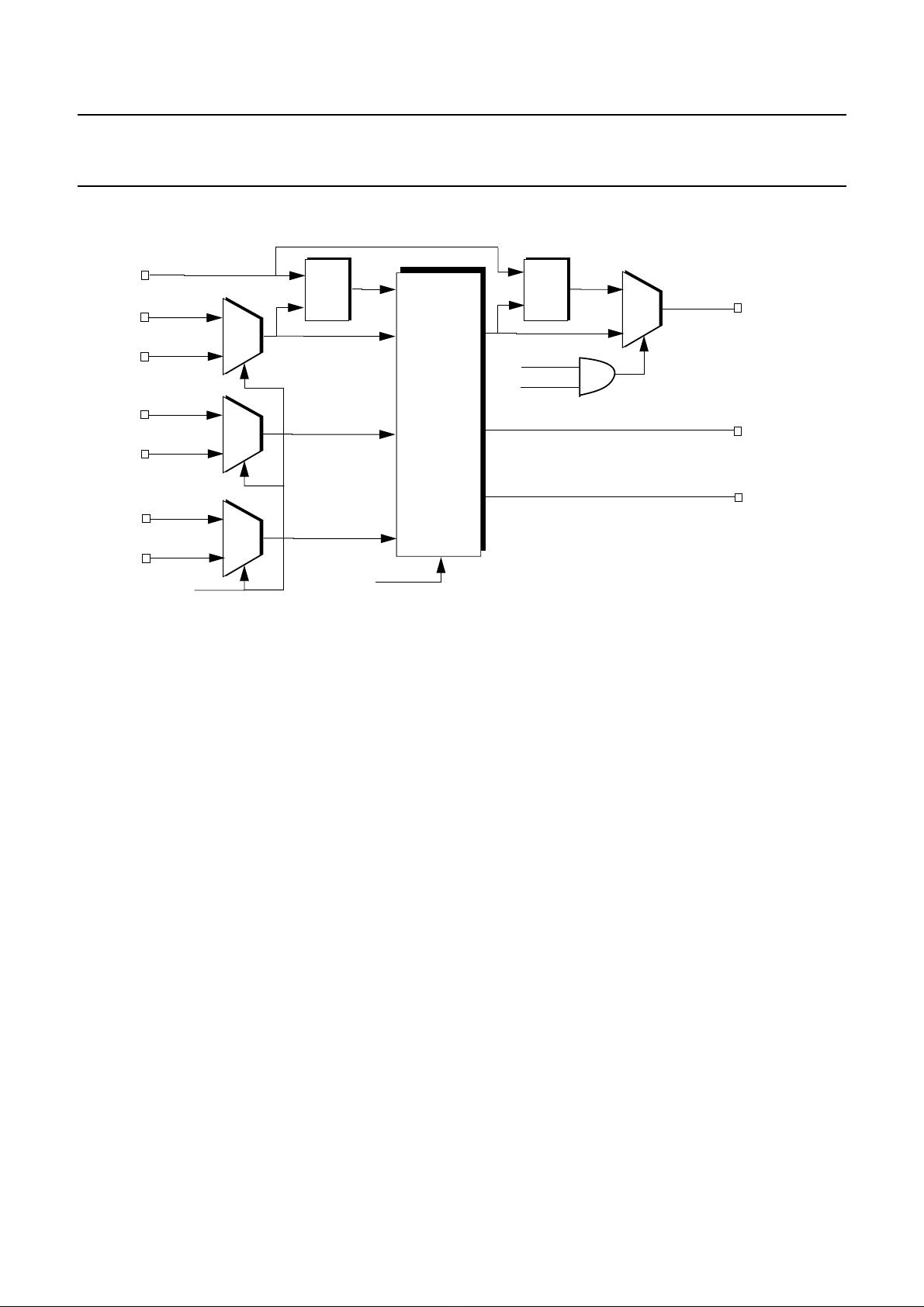
As shown in Figure 1 , the destination
routing memory defines the Local Bus to
SCbus switch connection. There are 128
destination routing memory locations
— one for each Local Bus input channel.
The data stored in the destination routing memory selects the timeslot and
SCbus serial port connection for the
Local Bus input channel. The source
routing memory defines the SCbus to
Local Bus switch connection. There are
128 source routing memory locations —
one for each Local Bus output channel.
The data stored in the source routing
memory selects the time slot and SCbus
serial port connection for the Local Bus
output channel.
2000 Sep 07 12
Page 13

Philips Semiconductors Preliminary specification
Universal Timeslot Interchange SC4000
Writing to the routing memory is synchronized with SCbus timing. So routing information can be changed only on
time slot boundaries. All input data is
buffered in holding registers. The entire
holding register is transferred to the output registers on a frame boundary basis.
All frame-bounded time slots incur a
one frame delay as they pass through the
switch. Switching data in this fashion
supports time slot bundling.
The SO outputs are tri-state controlled
on time slot boundaries by the Source
Routing Memory Switch Output Enable
Bit. This allows SO outputs from multiple devices to be connected to a common line. The data sample position of
both the SCbus and the Local bus can be
selected for either 50% or 75% of the bit
cell.
In addition to switching local bus serial
data to and from the SCbus, the SC4000
provides a means of switching parallel
data through the microprocessor interface to the SCbus. A frame boundary interrupt helps control the timing of
parallel data accesses. Direct reading and
writing of parallel access register contents makes for an efficient data transfer.
When using direct access, the controlling processor places the address of the
target channel on the address bus. In
this way, data can be read or written in a
single cycle. To avoid data corruption,
the application should not access the
channel for a time period defined as four
clocks before and four clocks after the
frame boundary.
The Source Routing Memory Local
Connect Enable mode allows the switching of any destination channel to
Figure 1. Destination and Source Switch Function Block
1 OF 128 DESTINATION SWITCH
SI_[3:0]
D_[7:0]
W/R_N
INPUT
HOLDING
REGISTER
PARALLEL
ACCESS
REGISTER
O
I
PARALLEL
ACCESS
ENABLE
OUTPUT
HOLDING REGISTER
any source channel without SCbus
intervention. This mode accommodates
either serial or parallel data transfer.
Since data passes through the switch
twice in this mode, there is a two-frame
delay from input to output.
Diagnostic mode electrically disconnects
the SC4000 from the SCbus but allows
access through the local bus. This mode
is particularly useful for running board
diagnostics without upsetting the
SCbus. A Master Clock source is
required to run this mode.
The SC4000 pinout anticipates a future
version of the chip that includes an internal HDLC controller for the message
channel. To remain compatible with this
and other subsequent versions of the
SC4000, applications must write 0 to
all “Reserved (read only)” configuration
registers.
SD_[15:0]
TIMESLOT & PORT
OUTPUT ENABLE
LOCAL CONNECT BUS
DESTINATION
ROUTING MEMORY
1 OF 128 SOURCE SWITCH
OUTPUT
HOLDING
REGISTER
HOLDING
REGISTER
SO_[3:0]
SOURCE
ROUTING MEMORY
INTERNAL PARALLEL
ACCESS
READ
OUTPUT
ENABLE
2000 Sep 07 13
INPUT
TIMESLOT,
PORT AND LOCAL
CONNECT ENABLE
Page 14

Philips Semiconductors Preliminary specification
Universal Timeslot Interchange SC4000
FUNCTION DESCRIPTION
Switching
The SC4000 allows data switching
through the microprocessor interface in
any of the following three directions:
• From any local bus serial channel (SI)
or parallel data bus D_[7:0] input to
any SCbus channel (SD) output
• From any SCbus channel (SD) input
to any output of the local bus serial
channel (SO) or parallel data bus
D_[7:0]
• From any of local bus serial channel
(SI) or parallel data bus D_[7:0] input
directly through an internal local
connect bus to any local bus serial
channel (SO) output
As shown in Figure 1, each input SI and
output SO channel is mapped to one of
128 unique locations in the destination
routing memory and source routing
memory, respectively. So data stored in
the destination or source routing memory selects the timeslot and serial port of
the SCbus. All data is buffered through
the input holding register, output holding register or parallel access register for
a switching matrix with one frame delay.
PLL Timing and Clock Control
The SC4000 provides the option of using the internal master PLL (C_43 = 0)
or an external master PLL (C_43 = 1).
As shown in Figure 2, the internal
master PLL generates a clock that is frequency-locked to an 8 KHz reference input of either SREF_8K or REF_8K[3:0].
When the SC4000 is enabled as SCbus
master (C_0 =1), a state machine inside
the SC4000 uses this clock to generate
Figure 2. Internal Master PLL (C_43 = 0) Function Block
EXTERNAL
CRYSTAL or OSC
REF_8K_[3:0]
4, 5, 6, 7
C_[42:40]
X_OUT
1
Master PLL
Reference
8 K Select
X_IN
2
65.536 MHz
SCbus
Clock
Master PLL
C_2
C_[10:8], C_[5:4]
Programmable
Divider
SCLK, SCLKX2N and a “free-running”
FSYNCN signal based on the speed of
the SCbus and the clock frequency. The
internal master PLL runs free when:
• Put into free run mode (ignoring
reference input changes) by control
C_[42:40]
• The 8 KHz reference input is static
“1” or “0”
• The input of X_IN is less than 65.536
MHz.
The internal master PLL can also generate an interrupt if it cannot lock the
selected 8 KHz reference input.
C_0, C_3, C_[23:22]
SCLKX2N
SCLKX2NA
46, 47
FSYNCN
FSYNCNA
54, 55
SCLK
SCLKA
49, 50
To Internal Watchdogs and
SCbus Error Detectors
Primary
or
Alternate
C_[45:44]
SCbus
SREF_8K
Source
Select
Select
C_3, C_23, C_46
2000 Sep 07 14
SREF_8K
SREF_8KA
51, 52
Page 15

Philips Semiconductors Preliminary specification
Universal Timeslot Interchange SC4000
Figure 3 shows an external master PLL
implementation. The SC4000 provides
the 8 KHz reference output signal
REF_8K_OUT (pin 7) to the external
PLL. This 8 KHz reference signal is
sourced from either REF_8K[1:0] or
SREF_8K. The output of the external
PLL is then routed back to the SC4000
via CLK_IN (pin 6). The master clock
input (CLK_IN) frequency select at
C_[10:8] would then be programmed
for the external PLL frequency.
As shown in Figure 4, the SC4000 also
provides an internal clock PLL and local
bus PLL timing control circuitry for
both SCbus master and slave operations.
The internal clock PLL is used to create
the 4.096 or 8.192 MHz timing slaved to
the SCbus when the local bus is running
faster than the SCbus (i.e., 2.048 MHz at
SCbus, 8.096 MHz at local bus). If the
SCbus is faster or equal to the local bus,
then the SCbus clocks serve as the internal clock and use to create the local bus
clocks as well as message channel clock.
The local bus clock PLL is used to create
a 2.048 MHz L_CLK when:
• Local bus framing mode C_[7:6] is set
to 2.048 Mb/s
• A 65.536 MHz clock is supplied on
X_IN
• The C_29 bit is set to one.
If SCLK stops transitionally such as
during a clock fail condition (CLKFAIL
= 1), then the local bus clock PLL runs
free to generate L_CLK clock. In addition, the local bus SO lines are tri-stated
so that the network interface can continue to run.
Interrupts Control
The SC4000 can interrupt the host CPU
with the interrupt request signal INT_0
Figure 3. External Master PLL (C_43 = 1) Function Block
REF_8K_OUT
External
PLL
7
REF_8K_[1:0]
4, 5
C_[42:40]
Master PLL
Reference
8 K Select
(pin 14). This signal is configured and
unmasked by configuration register bits
C_55, C_54 and C_53. The interrupt
sources are:
• C_56 SCbus CLKFAIL
• C_57 Frame Boundary
• C_58 Internal Master PLL Error
• C_59 SCbus Error Indicator (logical
“OR” of C_[67:64], C_[74:72], and
C_[83:80])
The interrupts are structured this way to
improve performance by allowing a single read operation (of configuration register byte 7) to determine whether the
SC4000 is the source of the interrupt.
Each of the SC4000 interrupt sources
can be individually masked.
C_0, C_3, C_[23:22]
SCLKX2N
SCLKX2NA
46, 47
FSYNCN
FSYNCNA
54, 55
SCLK
SCLKA
49, 50
C_2
C_[10:8], C_[5:4]
Programmable
Divider
To Internal Watchdogs and
SCbus Error Detectors
CLK_IN
6
Primary
or
Alternate
C_[45:44]
SCbus
SREF_8K
Source
Select
Select
C_3, C_23, C_46
2000 Sep 07 15
SREF_8K
SREF_8KA
51, 52
Page 16
Philips Semiconductors Preliminary specification
Universal Timeslot Interchange SC4000
Figure 4. Internal PLL and Local Bus PLL Timing Function Block
X_IN
2
SCLK
49
SCLKA
50
SCLKX2N
46
SCLKX2NA
47
FSYNCN
54
FSYNCNA
55
65.536 MHz
C_2
Primary
or
Alternate
Select
Primary
or
Alternate
Select
Primary
or
Alternate
Select
Internal
Clock
PLL
Internal
Timing
Control
State
Machine
C_[7:6], C_[5:4]
Local
Bus
Clock
PLL
C_[7:6]=0X (2.048 Mb/s)
C_29=1
2.048 MHz
1
0
L_CLK
83
L_FS
84
MC_CLK
11
2000 Sep 07 16
Page 17

Philips Semiconductors Preliminary specification
Universal Timeslot Interchange SC4000
CLKFAIL Timing and Control
When an SC4000 is enabled to be clock
master (C_0 = 1), the chip drives clock
and frame sync signals to the SCbus and
pulls the CLKFAIL line low. If the
SC4000 is then disabled as clock master,
the internal state machine waits for the
next frame boundary and then stops
driving clock and frame sync signals.
Instead, it drives the CLKFAIL line high
for one clock before tri-stating it (CLKFAIL is pulled up with 4.7K on every
board). An “armed” clock master (C_1
= 1) contains logic that monitors the
CLKFAIL line (C_51 must be set). If
CLKFAIL is sampled high for two consecutive clock periods, then the C_0 bit
is automatically set; the armed master
then begins driving clock and frame
sync signals and pulls CLKFAIL low.
Since the internal state machine was
using the clock and frame sync signals
driven by the previous master, the new
master takes over without any framing
error. It is as if one clock period had
been stretched, as shown in Figure 14.
Message Channel Interface
The SC4000 is designed for use with an
HDLC controller to implement the message channel interface. The interface between an HDLC controller and SC4000
consists of the 2.048 MHz MC_CLK
(pin 11), TXD_0 (pin 9) and RXD (pin
10) lines. Data read from the SCbus MC
(pin 80) line is passed straight through
the SC4000 to the RXD output. Data
read from TXD_0 can be passed straight
through the SC4000 to the MC output,
or be buffered internally through a
clocked register. Buffering output data is
controlled by C_12. When the Message
Table 1. Configuration Register Setup for SCbus Clock Slave
Operation Mode Conguration Register Bits Setup Function Description
SCbus Slave C_0 = 0 SCbus clock master disabled (Default)
C_1 = 0 SCbus clock master disarmed (Default)
C_2 SCbus Primary or Alternate Select
C_3 = 0 Diagnostic mode disabled (Note)
C_[5:4] SCbus Framing mode to select one of the following rate:
C_[7:6] Local bus Framing mode to select one of the following rate:
Note: Default of all configuration register bits except C_3 are 0
0: Primary SCbus signals selected (Default)
1: Alternate SCbus signals selected
0X = 2.048 Mb/s, 256 Bits/Frame, 32 Timeslots/Frame (Default)
10 = 4.096 Mb/s, 512 Bits/Frame, 64 Timeslots/Frame
11 = 8.192 Mb/s, 1024 Bits/Frame, 128 Timeslots/Frame
0X = 2.048 Mb/s, 256 Bits/Frame, 32 Timeslots/Frame (Default)
10 = 4.096 Mb/s, 512 Bits/Frame, 64 Timeslots/Frame
11 = 8.192 Mb/s, 1024 Bits/Frame, 128 Timeslots/Frame
Channel is Disabled (C_15 = 1), TXD_0
is looped back to the RXD to allow
diagnostics to be run on the HDLC
controller.
Operation Mode and Configuration Register Setup
The SC4000 can be configured to function in five different modes shown in the
tables below:
• SCbus Clock Slave (Table 1)
• SCbus Clock Master (Table 2)
• SCbus Armed Clock Master (Table 3)
• MVIP Clock Master (Table 4)
• MVIP Clock Slave (Table 5)
Table 6 shows signals that are cross
referenced by SCbus and MVIP.
2000 Sep 07 17
Page 18

Philips Semiconductors Preliminary specification
Universal Timeslot Interchange SC4000
Table 2. Configuration Register Setup for SCbus Clock Master
Operation Mode Conguration Register Bits Setup Function Description
SCbus Master C_0 = 1 SCbus clock master enabled
C_1 = 0 SCbus clock master disarmed (Default)
C_2 SCbus Primary or Alternate Select
C_3 = 0 Diagnostic mode disabled
C_[5:4] SCbus Framing mode to select one of the following rate:
C_[7:6] Local bus Framing mode to select one of the following rate:
C_[10:8] Master clock input frequency select:
C_21 = 0 SCbus FSYNCN rate to select one SCLK period (Default)
C_22 SCbus SCLKX2N and SCLKX2NA output enable control
C_23 SCbus Alternate signals output enable control
C_[43:40] (Internal/External
Master PLL reference 8K select)
0: Primary SCbus signals selected (Default)
1: Alternate SCbus signals selected
0X = 2.048 Mb/s, 256 Bits/Frame, 32 Timeslots/Frame (Default)
10 = 4.096 Mb/s, 512 Bits/Frame, 64 Timeslots/Frame
11 = 8.192 Mb/s, 1024 Bits/Frame, 128 Timeslots/Frame
0X = 2.048 Mb/s, 256 Bits/Frame, 32 Timeslots/Frame (Default)
10 = 4.096 Mb/s, 512 Bits/Frame, 64 Timeslots/Frame
11 = 8.192 Mb/s, 1024 Bits/Frame, 128 Timeslots/Frame
000 = 2.048 MHz (Default), 001 = 4.096 MHz, 010 = 8.192 MHz,
011 = 16.384 MHz, 100 = 32.768 MHz, 101= 65.536 MHz,
11X =Reserved
0: SCbus SCLKX2N and SCLKX2NA output enabled (Default)
1: SCbus SCLKX2N and SCLKX2NA output disabled
0: SCbus Alternate signals output disabled (Default)
1: SCbus Alternate signals output enabled
Internal/External Master PLL reference select:
If C_43 = 0 select the reference for the internal master PLL from C_[42:40]: 000 = Free-run (Default),
001/010 = Free-run,
011 = SREF_8K/SREF_8KA, 100 = REF_8K_0, 101 = REF_8K_1,
110 = REF_8K_2, 111 = REF_8K_3
(see Figure 2)
If C_43 = 1 select the reference for the external master PLL (output on REF_8K_OUT pin 7) from
C_[42:40]: 000 = Free-run (driven high) (Default), 001/010 = Free-run (driven high), 011 =
SREF_8K/SREF_8KA,
100 = REF_8K_0, 101 = REF_8K_1, 110/111 = Tri-state (Z)
(see Figure 3)
C_51 = 1 SCbus CLKFAIL latch debounce enabled
2000 Sep 07 18
Page 19

Philips Semiconductors Preliminary specification
Universal Timeslot Interchange SC4000
Table 3. Configuration Register Setup for SCbus Armed Clock Master
Operation Mode Conguration Register Bits Setup Function Description
SCbus Armed Master C_0 = 0 SCbus clock master disabled initially
C_1 = 1 SCbus clock master armed. When CLKFAIL goes high, C_0 bit will be automatically set and SC4000
C_2 SCbus Primary or Alternate Select
C_3 = 0 Diagnostic mode disabled
C_[5:4] SCbus Framing mode to select one of the following rate:
C_[7:6] Local bus Framing mode to select one of the following rate:
C_[10:8] Master clock input frequency select:
C_21 = 0 SCbus FSYNCN rate to select one SCLK period (Default)
C_22 SCbus SCLKX2N and SCLKX2NA output enable control
C_23 SCbus Alternate signals output enable control
C_[43:40] (Internal/External
Master PLL reference 8K select)
becomes clock master
0: Primary SCbus signals selected (Default)
1: Alternate SCbus signals selected
0X = 2.048 Mb/s, 256 Bits/Frame, 32 Timeslots/Frame (Default)
10 = 4.096 Mb/s, 512 Bits/Frame, 64 Timeslots/Frame
11 = 8.192 Mb/s, 1024 Bits/Frame, 128 Timeslots/Frame
0X = 2.048 Mb/s, 256 Bits/Frame, 32 Timeslots/Frame (Default)
10 = 4.096 Mb/s, 512 Bits/Frame, 64 Timeslots/Frame
11 = 8.192 Mb/s, 1024 Bits/Frame, 128 Timeslots/Frame
000 = 2.048 MHz (Default), 001 = 4.096 MHz, 010 = 8.192 MHz,
011 = 16.384 MHz, 100 = 32.768 MHz, 101= 65.536 MHz,
11X =Reserved
0: SCbus SCLKX2N and SCLKX2NA output enabled (Default)
1: SCbus SCLKX2N and SCLKX2NA output disabled
0: SCbus Alternate signals output disabled (Default)
1: SCbus Alternate signals output enabled
Internal/External Master PLL reference select:
If C_43 = 0 select the reference for the internal master PLL from C_[42:40]: 000 = Free-run (Default),
001/010 = Free-run,
011 = SREF_8K/SREF_8KA, 100 = REF_8K_0, 101 = REF_8K_1,
110 = REF_8K_2, 111 = REF_8K_3
(see Figure 2)
If C_43 = 1 select the reference for the external master PLL (output on REF_8K_OUT pin 7) from
C_[42:40]: 000 = Free-run (driven high) (Default), 001/010 = Free-run (driven high), 011 =
SREF_8K/SREF_8KA,
100 = REF_8K_0, 101 = REF_8K_1, 110/111 = Tri-state (Z)
(see Figure 3)
C_51 = 1 SCbus CLKFAIL latch debounce enabled
2000 Sep 07 19
Page 20

Philips Semiconductors Preliminary specification
Universal Timeslot Interchange SC4000
Table 4. Configuration Register Setup for MVIP Clock Master
Operation Mode Conguration Register Bits Setup Function Description
MVIP Master C_0 = 1 MVIP clock master enabled
C_1 = 0 MVIP clock master disarmed (Default)
C_2 = 0 Primary SCbus signals selected (Default)
C_3 = 0 Diagnostic mode disabled (Note 1)
C_[5:4] =00 MVIP Framing mode to select only one rate:
C_[7:6] Local bus Framing mode to select one of the following rate:
C_[10:8] Master clock input frequency select:
C_21 = 1 MVIP F0/ rate to select one C4/ period
C_22 = 0 MVIP C4/ output enabled (Default)
C_23 =0 SCbus Alternate signals output disabled (Default)
C_[43:40] (Internal/External
Master PLL reference 8K select)
0X = 2.048 Mb/s, 256 Bits/Frame, 32 Timeslots/Frame (Default)
0X = 2.048 Mb/s, 256 Bits/Frame, 32 Timeslots/Frame (Default)
10 = 4.096 Mb/s, 512 Bits/Frame, 64 Timeslots/Frame
11 = 8.192 Mb/s, 1024 Bits/Frame, 128 Timeslots/Frame
000 = 2.048 MHz (Default), 001 = 4.096 MHz, 010 = 8.192 MHz,
011 = 16.384 MHz, 100 = 32.768 MHz, 101= 65.536 MHz,
11X =Reserved
Internal/External Master PLL reference select:
If C_43 = 0 select the reference for the internal master PLL from C_[42:40]: 000 = Free-run (Default),
001/010 = Free-run,
011 = SEC_8K, 100 = REF_8K_0, 101 = REF_8K_1,
110 = REF_8K_2, 111 = REF_8K_3
(see Figure 2)
If C_43 = 1 select the reference for the external master PLL (output on REF_8K_OUT pin 7) from
C_[42:40]: 000 = Free-run (driven high) (Default), 001/010 = Free-run (driven high), 011 = SEC_8K,
100 = REF_8K_0, 101 = REF_8K_1, 110/111 = Tri-state (Z)
(see Figure 3)
Table 5. Configuration Register Setup for MVIP Clock Slave
Operation Mode Conguration Register Bits Setup Function Description
MVIP Slave C_0 = 0 MVIP clock master disabled (Default)
C_1 = 0 MVIP clock master disarmed (Default)
C_2 = 0 Primary SCbus signals selected (Default)
C_3 = 0 Diagnostic mode disabled
C_[5:4] = 00 MVIP Framing mode to select only one rate:
C_[7:6] Local bus Framing mode to select one of the following rate:
0X = 2.048 Mb/s, 256 Bits/Frame, 32 Timeslots/Frame (Default)
0X = 2.048 Mb/s, 256 Bits/Frame, 32 Timeslots/Frame (Default)
10 = 4.096 Mb/s, 512 Bits/Frame, 64 Timeslots/Frame
11 = 8.192 Mb/s, 1024 Bits/Frame, 128 Timeslots/Frame
2000 Sep 07 20
Page 21

Philips Semiconductors Preliminary specification
Universal Timeslot Interchange SC4000
Table 6. SCbus/MVIP Signals Cross Reference
SCbus 26-Pin Connector SCbus Signal MVIP Signal MVIP 40-Pin Connector
1 SCLKX2N C4/ 31
2 GND GND 30, 32
3 SCLK C2 35
4 SREF_8K SEC_8K 37
5 FSYNCN F0/ 33
6 CLKFAIL N/A N/A
7 SD_0 DSi0 8
8 GND GND 34
9 SD_1 DSo0 7
10 SD_2 DSi1 10
11 SD_3 DSo1 9
12 SD_4 DSi2 12
13 SD_5 DSo2 11
14 SD_6 DSi3 14
15 GND GND 36
16 SD_7 DSo3 13
17 SD_8 DSi4 16
18 SD_9 DSo4 15
19 SD_10 DSi5 18
20 SD_11 DSo5 17
21 GND GND 38
22 SD_12 DSi6 20
23 SD_13 DSo6 19
24 SD_14 DSi7 22
25 SD_15 DSo7 21
26 MC N/A N/A
2000 Sep 07 21
Page 22

Philips Semiconductors Preliminary specification
Universal Timeslot Interchange SC4000
Register Access Schemes
The SC4000 features two address access
schemes. One is an indirect access
scheme (C_11 = 0) to reduce the number of pins required for the micropro-
cessor address bus interface from nine to
two (A_[1:0]), as shown in Figure 5. The
other is a combination of both indirect
and direct parallel access schemes (C_11
= 1). Using the combination requires
Figure 5. Using Two Pins A_[1:0] for Address Bus Interface Scheme (C_11 = 0)
Address Data
03h High Byte Data Register (HBDR)
02h Low Byte Data Register (LBDR)
01h Internal Address Register (IAR)
00h Command/Status Register (CSR)
A_[1:0] D_[7:0]
FFh - E0h Source Parallel Access (31 - 0)
DFh - C0h Destination Parallel Access (31 - 0)
BFh - A0h Source Routing Memory (31 - 0)
9Fh - 80h Destination Routing Memory (31 - 0)
7Fh - 0Dh Reserved
0Ch - 00h Configuration Register (12 - 0)
Note: See bit 5 and 4 of CSR to select
the bank of channels
Microprocessor
Figure 6. Using Nine Pins A_[8:0] for Address Bus Interface Scheme (C_11 = 1)
Address Data
1FFh - 180h Source Parallel Access (127 - 0)
17Fh - 100h Destination Parallel Access (127 - 0)
FFh - 04h Reserved
03h High Byte Data Register (HBDR)
02h Low Byte Data Register (LBDR)
01h Internal Address Register (IAR)
00h Command/Status Register (CSR)
A_[8:0] D_[7:0]
FF - E0 Source Parallel Access (31 - 0)
DF - C0 Destination Parallel Access (31 - 0)
BF - A0 Source Routing Memory (31 - 0)
9F - 80 Destination Routing Memory (31 - 0)
7F - 0D Reserved
0C - 00 Configuration Register (12 - 0)
Note: See bit 5 and 4 of CSR to select
the bank of channels
that all nine microprocessor address
pins (A_[8:0]) be used, as shown in
Figure 6.
Microprocessor
2000 Sep 07 22
Page 23

Philips Semiconductors Preliminary specification
Universal Timeslot Interchange SC4000
MICROPROCESSOR INTERFACE
I/O Address Map
With Direct R/W to Parallel Access
Registers Disabled (C_11=0) (default)
A_[1:0] REGISTER
3h High Byte Data Register (HBDR)
2h Low Byte Data Register (LBDR)
1h Internal Address Register (IAR)
0h Command / Status Register
With direct R/W to Parallel Access
Register Enable (C_11=1)
A_[8:0] REGISTER
1FFh:180h Source Parallel Access Register
Ch. 127:0
17Fh:100h Destination Parallel Access Register
Ch. 127:0
0FFh:004h Reserved
003h High Byte Data Register (HBDR)
002h Low Byte Data Register (LBDR)
001h Internal Address Register (IAR)
000h Command / Status Register
Command / Status Register (Address = 0h)
D_[7:0] Definition
0 Busy (Read only)
1 Read Command (Write only)
2 Write Command (Write only)
3 Terminate Command (Read/Write)
[5:4] Channel Bank Select Register [1:0]
(Read/Write)
6 Channel Bank Select Register Enable
(Write only)
7 Reset (Read/Write)
Note: Setting more than one command
(Read, Write, Terminate or Reset) during an access to the Command/Status
register is not recommended.
Busy (D_0) (Read Only)
This bit is set (“1”) when a command
that requires synchronization with the
SC4000’s internal state machine has
been initiated. This bit clears (“0”)
when the command is completed.
The following commands require
synchronization:
• Destination Routing Memory
Write command
• Source Routing Memory Write
command
• Indirect Parallel Access Destination
Write command
• Indirect Parallel Access Source
Read command
Read (D_1) (Write only)
Setting this bit (“1”) initiates a read of
the register pointed to by the Internal
Address Register. When the Busy bit is
clear (“0”), the contents of the register
to be read are available by reading the
Low byte & HighByte Data register. It is
not necessary to clear (“0”) this bit after
it has been set (“1”).
Note: Set this bit for an Indirect Parallel
Access Source Read (this is the only
“READ” requiring synchronization).
For reads which do not require synchronization, the data registers can be read
immediately after writing the internal
address register.
Write (D_2) (Write only)
Setting this bit (“1”) initiates a write
to the register selected by the Internal
Address Register. When the Busy bit is
clear (“0”), the contents of the target
register have been updated using the
data stored in the Low Byte & High Byte
Data Register. It is not necessary to clear
(“0”) this bit after it has been set (“1”).
Terminate (D_3) (Read/Write)
Setting this bit (“1”) terminates a command that requires synchronization
with the SC4000’s internal state machine. This is necessary to complete a
command when the SC4000’s internal
state machine has stopped running (no
SCLK). The command in process is
completed asynchronously and the
Busy bit is cleared. It is necessary to clear
(“0”) this bit after it has been set (“1”).
Note: A new command (Read or Write)
should not be issued until after the
Terminate bit is cleared (“0”).
Channel Bank Select Register
[1:0] (D_[5:4]) (Read/Write)
This field determines the bank of channels that a command will affect. The
Channel Bank Select Register field is
combined with the Internal
Address Register to provide access to the
channel specific registers (routing and
parallel access). D_[5:4]) selects the
bank of channels to be accessed. This
field is cleared (“00”) on reset.
D_[5:4] = 00 -> Ch. 0 - 31
D_[5:4] = 01 -> Ch.32 - 63
D_[5:4] = 10 -> Ch.64 - 95
D_[5:4] = 11 -> Ch.96 - 127
Channel Bank Select Register Enable
(D_6) (Write only)
Writing to the command register with
this bit set (“1”) enables the Channel
bank select field to be changed. Writing
to the command register with this bit
cleared (“0”) causes the Channel Bank
Select Register field to retain its previous
value.
Note 1: The Channel Bank Select Register may be changed during a write cycle
which also initiates a Read or Write
command. The Read or Write command affects the register pointed to by
the new value written into the Channel
Bank Select Register.
Note 2: The Channel Bank Select Register should not be changed if the microprocessor interface is busy.
Note 3: The Channel Bank Select Register should not be changed during a write
cycle that either sets (0->1) or clears
(1->0) the Terminate command.
2000 Sep 07 23
Page 24

Philips Semiconductors Preliminary specification
Reset (D_7) (Read/Write)
Internal Address Register Map Low Byte Data Register (Address = 02h)
Universal Timeslot Interchange SC4000
Setting this bit (“1”) puts the SC4000 in
reset and initializes the Configuration,
Routing and Parallel Access Registers.
This command is analogous to the function of the RESET pin. Clearing this bit
(“0”) returns the SC4000 to normal operation, ready for configuration.
Internal Address Registerr (Address = 01h)
D_[7:0] Definition
7:0 Internal Address Register (IAR_[7:0])
IAR_
[7:0]
FFh:80h Channel Spe-
7Fh:0Dh Reserved
0Ch:00h Configuration
Register IAR_
[7:0]
FFh:E0h Source
cific Registers
DFh:C0h Destination
BFh:A0h Source
9Fh:80h Destination
Registers
Register
Parallel
Access
Parallel
Access
Routing
Memory
Routing
Memory
D_[7:0] Definition
7:0 Low byte Data Register (LBDR_[7:0])
High Byte Data Register (Address = 03h)
D_[7:0] Definition
7:0 High byte Data Register (HBDR_[7:0])
2000 Sep 07 24
Page 25

Philips Semiconductors Preliminary specification
Universal Timeslot Interchange SC4000
Channel Specific Registers
The Channel Specific Registers are
divided into four groups. A group is selected by bits 5 through 7 of theinternal
address register.
Channel Specific Registers Map
IAR[7:0] CBSR_[1:0] = 00 CBSR_[1:0] = 01 CBSR_[1:0] = 10 CBSR_[1:0] = 11
IAR_[7:5]
FFh - E0h
Source
Parallel
Access
IAR_[7:5]
DFh - C0h
Destination
Parallel
Access
IAR_[7:5]
BFh - A0h
Source
Routing
Memory
IAR_[7:5]
9Fh - 80h
Destination
Routing
Memory
IAR_[4:0] = 1Fh Ch. 31 Ch. 63 Ch. 95 Ch. 127
IAR_[4:0] = 1Eh Ch. 30 Ch. 62 Ch. 94 Ch. 126
. . . . .
. . . . .
IAR_[4:0] = 01h Ch. 1 Ch. 33 Ch. 65 Ch. 97
IAR_[4:0] = 00h Ch. 0 Ch. 32 Ch. 64 Ch. 96
IAR_[4:0] = 1Fh Ch. 31 Ch. 63 Ch. 95 Ch. 127
IAR_[4:0] = 1Eh Ch. 30 Ch. 62 Ch. 94 Ch. 126
. . . . .
. . . . .
IAR_[4:0] = 01h Ch. 1 Ch. 33 Ch. 65 Ch. 97
IAR_[4:0] = 00h Ch. 0 Ch. 32 Ch. 64 Ch. 96
IAR_[4:0] = 1Fh Ch. 31 Ch. 63 Ch. 95 Ch. 127
IAR_[4:0] = 1Eh Ch. 30 Ch. 62 Ch. 94 Ch. 126
. . . . .
. . . . .
IAR_[4:0] = 01h Ch. 1 Ch. 33 Ch. 65 Ch. 97
IAR_[4:0] = 00h Ch. 0 Ch. 32 Ch. 64 Ch. 96
IAR_[4:0] = 1Fh Ch. 31 Ch. 63 Ch. 95 Ch. 127
IAR_[4:0] = 1Eh Ch. 30 Ch. 62 Ch. 94 Ch. 126
. . . . .
. . . . .
IAR_[4:0] = 01h Ch. 1 Ch. 33 Ch. 65 Ch. 97
IAR_[4:0] = 00h Ch. 0 Ch. 32 Ch. 64 Ch. 96
IAR_[7:5]
100 -> Destination Routing Memory
101 -> Source Routing Memory
110 -> Destination Parallel Access
111 -> Source Parallel Access
D_[5:4] of Command/Status Register (D_6 = 1)
Channels within these groups are selected by bits 4 through 0 (IAR_[4:0]) of
the Internal Address Register and bits 1
and 0 (D_[5:4] Command/Status Register) of the Channel Bank Select Register
(CBSR)
2000 Sep 07 25
Page 26

Philips Semiconductors Preliminary specification
Universal Timeslot Interchange SC4000
Destination Routing Memory—Low Byte
LBDR_[7:0] Definition
[6:0] Time-slot Select [6:0]
7 Reserved
Time-Slot Select [6:0] (Read/write)
This field selects the SCbus Time-Slot
that a Destination Channel is routed to.
00h -> SCbus Time-Slot 0 (Default)
01h -> SCbus Time-Slot 1
02h -> SCbus Time-Slot 2
.
.
7Eh -> SCbus Time-Slot 126
7Fh -> SCbus Time-Slot 127
Destination Routing Memory— High Byte
HBDR_[7:0] Definition
[3:0] Port Select [3:0]
[5:4] Reserved
6 Parallel Access Enable
7 Switch Output Enable
Port Select [3:0] (Read/Write)
This field selects the SCbus Port that a
Destination Channel is routed to.
0h -> SCbus SD_0 (Default)
1h -> SCbus SD_1
2h -> SCbus SD_2
.
.
Eh -> SCbus SD_14
Fh -> SCbus SD_15
Parallel Access Enable (Read/Write)
This bit enables the Destination Parallel
Access channel to be output in place of
the SI Local Bus serial stream.
0 -> Parallel Access Disabled (Default)
1 -> Parallel Access Enabled
Switch Output Enable (Read/Write)
This bit enables the Switch Output to
the SCbus.
0 -> Output Disabled (Default)
1 -> Output Enabled
Source Routing Memory— Low Byte
LBDR_[7:0] Definition
[6:0] Time-Slot/Channel Select [6:0]
7 Reserved
Time-Slot/Channel Select [6:0] (Read/Write)
If Local Connect is disabled (default)
this field selects the SCbus Time-Slot
that is routed to a Source Channel.
00h -> SCbus Time-Slot 0 (Default)
01h -> SCbus Time-Slot 1
02h -> SCbus Time-Slot 2
.
.
7Eh -> SCbus Time-Slot 126
7Fh -> SCbus Time-Slot 127
If Local Connect is enabled this field
selects the Destination Channel that
is routed to a Source Channel.
00h -> Destination Channel 0 (Default)
01h -> Destination Channel 1
02h -> Destination Channel 2
.
.
7Eh -> Destination Channel 126
7Fh -> Destination Channel 127
Source Routing Memory—High byte
HDBR_[7:0] Definition
[3:0] Port Select [3:0]
[5:4] Reserved
6 Local Connect Enable
7 Switch Output Enable
Port Select [3:0] (Read/Write)
This field selects the SCbus Port that is
routed to a Source Channel.
0h -> SCbus SD_0 (Default)
1h -> SCbus SD_1
2h -> SCbus SD_2
.
.
Eh -> SCbus SD_14
Fh -> SCbus SD_15
If Local Connect is enabled this field is
don’t care.
Local Connect Enable (Read/Write)
This bit enables the Local Connection
of a Destination Channel to a Source
Channel.
0 -> Local Connect Disabled (Default)
1 -> Local Connect Enabled
Switch Output Enable (Read/Write)
This bit enables the Switch Output to
the Local Bus.
0 -> Output Disabled (Default)
1 -> Output Enabled
Parallel Access
The parallel access channels can be accessed two ways: Indirect and Direct.
Destination Parallel Access
LBDR_[7:0] Definition
[7:0] Serial Data Bit [1:8]
Serial Data [1:8] (Read/Write)
This register contains the byte to be
transmitted when Destination Routing
Memory Parallel Access is enabled
Note: When converted from parallel
to serial, bit 1 is transmitted first.
Note: This register is cleared (“00”)
on Reset.
Source Parallel Access
LBDR_[7:0] Definition
[7:0] Serial Data Bit [1:8]
Serial Data [1:8] (Read Only)
This register contains the byte received
from the Source Channel selected by the
Source Routing Memory.
Note: When converted from serial to
parallel, bit 1 is received first.
2000 Sep 07 26
Page 27

Philips Semiconductors Preliminary specification
SCbus Primary/Alternate Select (C_2)
Configuration Register Byte 1, IAR = 01H
Universal Timeslot Interchange SC4000
CONFIGURATION REGISTERS
Configuration Register Byte 0, IAR = 00H
LBDR_[7:0] C_[7:0] Definition
0 0 SCbus Clock Master
1 1 SCbus Clock Master
2 2 SCbus Primary/
3 3 Diagnostic Mode
[5:4] [5:4] SCbus Framing Mode
[7:6] [7:6] Local Bus Framing
Arm
Alternate Select
Enable
[1:0]
Mode [1:0]
SCbus Clock Master (C_0) (Read/Write)
This bit is synchronized with the Master
Clock Input enables the SC4000 to start
and stop being SCbus Clock Master.
0-> SCbus Clock Master Disabled
(Default)
1-> SCbus Clock Master Enabled
Note: With IAR=00H and LBDR D_0=0
issue Terminate command to asynchronously stop being SCbus Clock Master
when no Master Clock Input is present
(i.e dead clock)
SCbus Clock Master Arm (C_1) (Read/Write)
The process of becoming SCbus Clock
Master can be sped up by arming the
SC4000 which is intended to become
clock master in the event of a clock failure. When a SC4000 is armed and CLKFAIL=1 the C_0 bit is automatically set.
The SC4000 begins driving the SCbus
within 4 clocks of CLKFAIL going high.
0-> SCbus Clock Master Disarmed
(Default)
1-> SCbus Clock Master Armed
Note: C_51 SCbus CLKFAIL Debounce
Enable must be set to use this feature.
(Read/Write)
The SC4000 provides Alternate SCbus
signals for fault tolerance. This bit controls internal signal selection.
0->Primary SCbus signals selected
(Default)
1->Alternate SCbus Signals selected
Diagnostic Mode Enable (C_3) (Read/Write)
In Diagnostic Mode the SC4000’s SCbus
output drivers and receivers are electrically disconnected from the SCbus. Internally, the SCbus outputs are looped
back to their corresponding inputs. This
creates a virtual SCbus within the
SC4000 that can be used to test thoroughly the SC4000 without disrupting
normal SCbus traffic.
0->Diagnostic Mode Disabled
1->Diagnostic Mode Enabled (default)
Note 1: Diagnostic Mode is Enabled
when the SC4000 is reset.
Note 2: A clock must be present at the
Master Clock input to use this mode.
SCbus Framing Mode [1:0](C_[5:4])
(Read/Write)
0x -> 2.048 Mb/s, 256 Bits/Frame, 32
Timeslots/Frame (Default)
10 -> 4.096 Mb/s, 512 Bits/Frame, 64
Timeslots/frame
11 -> 8.192 Mb/s, 1024 Bits/Frame, 128
Timeslots/Frame
Local bus Framing Mode [1:0](C_[7:6])
(Read/Write)
0x -> 2.048 Mb/s, 256 Bits/Frame, 32
Timeslots/Frame (Default)
10 -> 4.096 Mb/s, 512 Bits/Frame, 64
Timeslots/frame
11 -> 8.192 Mb/s, 1024 Bits/Frame,
128 Timeslots/Frame
Note: If the Local Bus framing mode
selection is for a higher data rate than
that of the SCbus framing mode, then a
65.536 MHz clock must be provided on
X_IN.
LBDR_[7:0] C_[15:8] Definition
[2:0] [10:8] Master Clock Input
Frequency Select [2:0]
3 11 Direct R/W to Parallel
Access Registers
Enable
4 12 Message Channel
Registered TXD Enable
5 13 Message Channel
TXD_0 or TXD_1
(internal HDLC) Select
6 14 Message Channel
Clock Duty Cycle
Select
7 15 Message Channel
Output Disable
(w/Loopback)
Master Clock Input Frequency Select
[2:0] (C_[10:8]) (Read/Write)
000-> 2.048 MHz (Default)
001-> 4.096 MHz
010-> 8.192 MHz
011->16.384 MHz
100-> 32.768 MHz
101-> 65.536 MHz
110-> Reserved
111-> Reserved
Note: The Master Clock Input may be
sourced from either X_IN or CLK_IN
(see C_43).
Direct R/W to Parallel Access Registers
Enable (C_11) (Read/Write)
0-> Direct R/W Disabled (Default)
1-> Direct R/W Enabled
Note: When Disabled A_[8:2] is don’t
care. When Enabled address setup to
falling edge of WR_N or STRB_N is
required.
Message Channel Registered TXD Enable
(C_12) (Read/Write)
0-> TXD Passed Through onto MC
(Default)
1-> TXD Registered onto MC
2000 Sep 07 27
Page 28

Philips Semiconductors Preliminary specification
Universal Timeslot Interchange SC4000
Note: When C_12=0 the HDLC Controller must be programmed to output
TXD on the Rising edge of MC_CLK.
When C_12=1 the HDLC controller
must be programmed to output TXD on
the falling edge of MC_CLK.
Message Channel TXD_0 or TXD_1 Select
(C_13) (Read/Write)
0-> TXD_0 External HDLC Controller
(Default)
1-> TXD_1 Future Internal HDLC
Controller
Note: If TXD_1 is selected on an SC4000
without an Internal HDLC Controller
all 1’s will be output on MC (idle).
Message Channel Clock Duty Cycle Select
(C_14) (Read/Write)
0-> 50% (Default)
1-> 75% (2 &4 Mb/s SCbus modes),
62.5% (8 Mb/s SCbus)
Note: SCLKX2N must be present to
select 75% when SCbus is 2 Mb/s.
Message Channel Output Disable
(W/ loopback) (C_15) (Read/Write)
0-> Message Channel Output Enabled
(Default)
1-> Message Channel Output Disabled
Note: When the Message Channel is Dis-
abled, TXD is looped back to the RXD to
allow diagnostics runs on the HDLC
Controller.
Configuration Register Byte 2, IAR = 02H
LBDR_[7:0] C_[23:16] Definition
0 16 SCbus SD Sample
Position
1 17 Local bus SI Sample
Position
2 18 SCbus SD Output
Delay Enable
3 19 Local bus SO Output
Delay Enable
4 20 SCbus FSYNCN
Sample position
5 21 SCbus FSYNCN Rate
6 22 SCbus SCLKX2N,
SCLKX2NA Output
Disable
7 23 SCbus Alternate (A)
Signals Output Enable
SCbus SD Sample Position (C_16)
(Read/Write)
0-> Sample at 50% of Bit Cell (Default)
1-> Sample at 75% of Bit Cell
Note: SCLKX2N must be present to
select 75% sample.
Local Bus SI Sample Position (C_17)
(Read/Write)
0-> Sample at 50% of Bit Cell (Default)
1-> Sample at 75% of Bit Cell
Note 1: To select 75% sample,SCLKX2N
must be present or the local bus framing
mode must be set to a data rate that is either higher or lower than the SCbus
framing mode.
Note 2: To select 75% sample (C_17=1),
it is not necessary to select the L_CLK
rate equal to 2X (C_28=1)
SCbus SD Output Delay Enable (C_18)
(Read/Write)
To avoid bus contention, enabled SCbus
SD outputs are delayed when coming
out of tri-state.
0-> SCbus SD Output Delay Disabled
(Default)
1-> SCbus SD Output Delay Enabled
Local bus SO Output Delay Enable (C_19)
(Read/Write)
To avoid bus contention, enabled local
bus SO outputs are delayed when coming out of tri-state.
0-> Local bus SO Output Delay Disabled (Default)
1-> Local bus SO Output Delay Enabled
SCbus FSYNCN Sample Position (C_20)
(Read/Write)
0-> Sample at rising edge of SCLK
(Default)
1-> Sample at rising edge of SCLKX2N
with SCLK high.
SCbus FSYNCN Rate (C_21) (Read/Write)
This bit determines the clock by which
the FSYNCN signal is generated.
0 -> 1 SCLK period (Default)
1 -> 1 SCLKX2N period
Note: This mode is provided for MVIP
compatibility.
SCbus SCLKX2N, SCLKX2NA Output
Disable(C_22) (Read/Write)
This bit disables the SCLKX2N and
SCLKX2NA outputs when they are not
required. When disabled, the outputs
are tri-stated.
0-> SCLKX2N and SCLKX2NA Outputs
Enabled (Default)
1-> SCLKX2N and SCLKX2NA Outputs
Disabled
2000 Sep 07 28
Page 29

Philips Semiconductors Preliminary specification
SCbus Alternate (A) Signals Output Enable
Local bus L_CLK & L_FS Rate (C_28)
Configuration Register Byte 4, IAR = 04H
Universal Timeslot Interchange SC4000
(C_23) (Read/Write)
This bit enables the SCbus Alternate
(“A”) Signals Output (when required).
When disabled, the outputs are
tri-stated.
0-> SCbus Alternate (“A”) Signals
Output Disabled (Default)
1-> SCbus Alternate (“A”) Signals
Output Enabled
Configuration Register Byte 3, IAR = 03H
LBDR_[7:0] C_[31:24] Definition
0 24 Local bus L_CLK
1 25 Local bus L_FS
[3:2] [27:26] Local bus L_FS
4 28 Local bus L_CLK
5 29 Local bus L_CLK
6 30 Local bus L_CLK
7 31 Reserved (0)
Local bus L_CLK Polarity (C_24)
(Read/Write)
0- > L_CLK Non-Inverted (Default)
1- > L_CLK Inverted
Local bus L_FS Polarity (C_25) (Read/Write)
0- > L_FS Non-Inverted (Default)
1- > L_FS Inverted
Local bus L_FS Position (C_[27:26])
(Read/Write)
00 -> L_FS occurs during the last clock
period of the frame (Default)
01 -> L_FS straddles the frame
boundary
10 -> L_FS occurs during the first clock
period of the frame
11 -> Reserved
Polarity
Polarity
Position [1:0]
and L_FS Rate
DPLL Enable
8.192 MHz 62.5%
duty cycle Enable
(Read only)
(Read/Write)
0 -> L_CLK & L_FS equal to the Local
bus data rate (Default)
1 -> L_CLK & L_FS equal to 2 times
the Local bus data rate
Note: To select the 2x rate, SCLKX2N
must be present or the Local bus framing mode must be set to a data rate that
is either higher or lower than the SCbus
framing mode.
Local bus L_CLK DPLL Enable (C_29)
(Read/Write)
This mode is provided to maintain a
continuous L_CLK for network interfaces during a Clock Fail condition.
0->L_CLK DPLL Disabled (Default)
1->L_CLK DPLL Enabled
Note 1: The Local bus Framing Mode
(C_[7:6]) must be set to 2.048 Mb/s and
a 65.536MHz Clock must be supplied on
X_IN.
Note 2: When Enabled L_CLK will run
free during an SCbus Clock Fail
condition.
Note 3: When the DPLL enters the freerun, the Local bus SO lines are tri-stated.
Local bus L_CLK 8.192 MHz 62.5% Duty
Cycle (C_30) (Read/Write)
0 -> L_CLK 8.192 MHz 62.5% Duty
Cycle Disabled (Default)
1 -> L_CLK 8.192 MHz 62.5% Duty
Cycle Enabled
Note: To enable L_CLK 8.192 MHz
62.5% Duty Cycle, the Local bus Framing Mode (C_[7:6]) must be set to 8.192
Mb/s and the SCbus Framing Mode
(C_[5:4]) must be set to 4.096 Mb/s or
2.048 Mb/s. C_28 must be set to 0.
LBDR_[7:0] C_[39:32] Definition
[3:0] [35:32] Revision field (read
only)
[7:4] [39:36] Version field (SC4000
= 1H, SC2000 = 0H)
(Read only)
Version/Revision Status (C_[39:32])
The Version/Revision Register is a read
only register. It is intended for use to
identify SCxxxx devices.
This field may be changed in future
SCxxxx designs. It is recommended that
a test of this field be included in all versions of firmware interface code.
The initial release of the SC4000 will be
Version/Revision = 10H
Configuration Register 5,IAR = 05H
LBDR_[7:0] C_[47:40] Definition
[2:0] [42:40] Master PLL Reference
Select [2:0]
3 43 Internal/External
Master PLL Select
[5:4] [45:44] SCbus SREF_8K
Source Select [1:0]
6 46 SCbus SREF_8K
Output Enable
7 47 SCbus SCLK 8.192
MHz 62.5% duty
cycle enable
Master PLL Reference Select [2:0]
(C_[42:40]) (Read/Write)
When C_43=0 this field selects the reference for the Internal Master PLL.
000 -> Free-run (Default)
001 -> Free-run
010 -> Free-run
011 -> SREF_8K
100 -> REF_8K_0
101 -> REF_8K_1
110 -> REF_8K_2
111 -> REF_8K_3
2000 Sep 07 29
Page 30

Philips Semiconductors Preliminary specification
Universal Timeslot Interchange SC4000
When C_43=1 this field selects the reference for the External Master PLL which
is output on REF_8K_OUT pin7.
000 ->Free-run (driven high) (Default)
001 ->Free-run (driven high)
010 ->Free-run (driven high)
011 -> SREF_8K
100 -> REF_8K_0
101 -> REF_8K_1
110 -> tri-state (Z)
111 -> tri-state (Z)
Internal/External Master PLL Select (C_43)
(Read/Write)
This bit selects the Master PLL to be
either Internal or External.
0 -> Internal Master PLL (Default)
1 -> External Master PLL
SCbus SREF_8K Source Select [1:0]
(C_[45:44]) (Read/Write)
00 -> REF_8K_0 (Default)
01 -> REF_8K_1
10 -> REF_8K_2
11 -> REF_8K_3
SCbus SREF_8K Output Enable (C_46)
(Read/Write)
0 -> SCbus SREF_8K Disabled (Z)
(Default)
1 -> SCbus SREF_8K Enabled
SCbus SCLK 8.192 MHz 62.5% Duty Cycle
(C_47) (Read/Write)
0 -> SCLK 8.192 MHz 62.5% Duty
Cycle Disabled (Default)
1 -> SCLK 8.192 MHz 62.5% Duty
Cycle Enabled
Note: The SCbus Framing Mode
(C_[5:4]) must be set to 8.192 Mb/s to
enable SCLK 8.192 MHz 62.5% duty
cycle. If Enable (C_22=0) SCLKX2N
will be driven high.
Configuration Register Byte 6, IAR = 06H
LBDR_[7:0] C_[55:48] Definition
0 48 Clock Watchdog
Enable
1 49 Microprocessor
Watchdog Enable
2 50 SCbus CLKFAIL
Latch Set Polarity
Select
3 51 SCbus CLKFAIL
Latch Debounce
Enable
4 52 Frame Boundary
Latch Set Delay Enable
5 53 INT_0 Mask_n
6 54 INT_0 Polarity
7 55 INT_0 Output Driver
Configuration
Clock Watchdog Enable (C_48) (Read/Write)
This bit enables the Clock Watchdog.
0 -> Clock Watchdog Disabled (Default)
1 -> Clock Watchdog Enabled
Note: When enabled, C_48 is read back a
1 until the Master PLL clocks for 125us
(+/- 50%); then it reads back a 0. This
mode is provided to allow detection of a
missing PLL clock. This information can
then be used to take a master off the bus
or to remove a secondary clock master
from the fallback list. The Clock Watchdog must be re-armed after each test. To
re-arm, the Clock Watchdog C_48 must
be cleared to “0” and then set to “1”.
Microprocessor Watchdog Enable (C_49)
(Read/Write)
This bit enables the Microprocessor
Watchdog.
0 -> Microprocessor Watchdog Disabled (Default)
1 -> Microprocessor Watchdog Enabled
Note: When enabled the SC4000 will be
put into reset after the Master PLL
clocks for 256 ms (+/-50%).
This mode is provided to force an
SC4000 off the SCbus when it’s controlling microprocessor fail to reset the
watchdog. Each time C_49 is cleared
“0” and the set “1” the watchdog count
is reset.
SCbus CLKFAIL Latch Set Polarity Select
(C_50) (Read/Write)
This bit selects the polarity of the SCbus
CLKFAIL signal that will set the
CLKFAIL latch.
0 -> CLKFAIL latch set when
CLKFAIL = 0 (Default)
1 -> CLKFAIL latch set when
CLKFAIL = 1
Note 1: The CLKFAIL polarity bit can be
used to generate interrupts on both ends
of a CLKFAIL transition. The CLKFAIL
= 0 interrupt is used by the new primary
clock source to determine that the transition from secondary to primary has
been made. The CLKFAIL = 1 interrupt
is used by a secondary clock source to
determine that the primary clock source
has given up the bus. A third module
(neither primary or secondary) could
use this interrupt to monitor the CLKFAIL transition and act as a system
watchdog.
Note 2: Only change CLKFAIL polarity
when CLKFAIL Latch Clear_N
(C_60) = 0.
SCbus CLKFAIL Latch Debounce Enable (C_51)
(Read/Write)
0 -> CLKFAIL Latch Debounce Disabled
(Default)
1 -> CLKFAIL Latch Debounce Enabled
Note 1: A clock must be present from the
Master PLL to enable this feature.
Note 2: The debounce logic requires that
the CLKFAIL signal be sampled with the
same value for two consecutive Master
PLL clocks before it can set the CLKFAIL Latch.
2000 Sep 07 30
Page 31

Philips Semiconductors Preliminary specification
Frame Boundary Latch Set Delay Enable
Configuration Register Byte 7, IAR = 07H
SCbus CLKFAIL Latch Clear_N (C_60)
Universal Timeslot Interchange SC4000
(C_52) (Read/Write)
0 -> Frame Boundary Latch Set at frame
boundary - no delay (Default)
1 -> Frame Boundary Latch Set is
delayed until after the input buffer to
output buffer transfer is complete (4
internal clocks after frame boundary).
Note 1: With direct W/R to Parallel Access Register Enabled (C_11=1), using
the delayed frame boundary interrupt
indicates that it is now safe to read from
and write to the Parallel Access Registers. To avoid data corruption, all access
must be completed 8 internal clocks
prior to the next delayed frame boundary interrupt.
Note 2: The internal clock is equal to
either the SCbus data rate or the Local
bus data rate whichever is faster.
INT_0 Mask_N (C_53) (Read/Write)
Clearing this bit(“0”) masks INT_0.
INT_0 is the logical OR of CLKFAIL
(C_56), Frame Boundary (C_57), Internal Master PLL Error (C_58) Latches
and SCbus Error (C_59) Indicator.
0 -> INT_0 Masked (Default)
1 -> INT_0 Enabled
Note: The INT_0 Mask bit can be used
to globally disable interrupt generation
while the state of the latches can continue to be polled through the microprocessor interface. This bit can also be
used to create edge-triggered interrupts.
INT_0 Output Polarity (C_54) (Read/Write)
0 -> INT_0 Active Low (Default)
1 -> INT_0 Active High
INT_0 Output Driver (C_55) (Read/Write)
0 -> Open Collector INT_0 Output
Driver (Default)
1 -> Totem-Pole INT_0 Output Driver
LBDR_[7:0] C_[63:56] Definition
0 56 SCbus CLKFAIL Latch
1 57 Frame Boundary
2 58 Internal Master PLL
3 59 SCbus Error Indicator
4 60 SCbus CLKFAIL Latch
5 61 Frame Boundary
6 62 Internal Master PLL
7 63 Reserved (0)
SCbus CLKFAIL Latch (C_56) (Read Only)
0 -> SCbus CLKFAIL Latch Clear
1 -> SCbus CLKFAIL Latch Set
Frame Boundary Latch (C_57) (Read only)
0 -> Frame Boundary Latch Clear
1 -> Frame Boundary Latch Set
Internal Master PLL Error Latch (C_58)
(Read Only)
This latch is set when the Internal Master PLL is not “locked” to its selected reference.
0 -> Internal Master PLL Error Latch
Clear
1 -> Internal Master PLL Error Latch Set
SCbus Error Indicator (C_59) (Read Only)
C_59 is the logical OR of C_[67:64],
C_[74:72] and C_[83:80].
0 -> All SCbus Error Latches Clear
1 -> one or more SCbus Error Latches
Set
(Read/Write)
0 -> SCbus CLKFAIL Latch held clear
(Default)
(Read only)
Latch (Read only)
1 -> SCbus CLKFAIL Latch enabled
Frame Boundary Latch Clear_N (C_61)
(Read/Write)
Error Latch
(Read only)
0 -> Frame Boundary Latch held clear
(Default)
1 -> Frame Boundary Latch enabled
(Read only)
Clear_n
Latch Clear_n
Internal Master PLL Error Latch Clear_N
(C_62) (Read/Write)
0 -> Internal Master PLL Error Latch
held clear (Default)
1 -> Internal Master PLL Error Latch
Error Latch Clear_n
enabled
Configuration Register Byte 8, IAR = 08H
(Read only)
LBDR_[7:0] C_[71:64] Definition
0 64 SCbus SCLKX2N
1 65 SCbus SCLKX2NA
2 66 SCbus SCLK Error
3 67 SCbus SCLKA Error
4 68 SCbus SCLKX2N
5 69 SCbus SCLKX2NA
6 70 SCbus SCLK Error
7 71 SCbus SCLKA Error
SCbus SCLKX2N Error Latch (C_64)
(Read Only)
The SCbus SCLKX2N Error Latch is
set when SCLKX2N does not transition
during the equivalent Master PLL clock
period.
0 -> SCbus SCLKX2N Error Latch Clear
1 -> SCbus SCLKX2N Error Latch Set
Error Latch
(Read only)
Error Latch
(Read only)
Latch (Read only)
Latch (Read only)
Error Latch Clear_n
Error Latch Clear_n
Latch Clear_n
Latch Clear_n
2000 Sep 07 31
Page 32

Philips Semiconductors Preliminary specification
Universal Timeslot Interchange SC4000
SCbus SCLKX2NA Error Latch (C_65)
(Read only)
The SCbus SCLKX2NA Error Latch is
set when SCLKX2NA does not transition during the equivalent Master PLL
clock period.
0 -> SCbus SCLKX2NA Error Latch
Clear
1 -> SCbus SCLKX2NA Error Latch Set
SCbus SCLK Error Latch (C_66) (Read only)
The SCbus SCLK Error Latch is set when
SCLK does not transition during the
equivalent Master PLL clock period.
0 -> SCbus SCLK Error Latch Clear
1 -> SCbus SCLK Error Latch Set
SCbus SCLKA Error Latch (C_67) (Read only)
The SCbus SCLKA Error Latch is set
when SCLKA does not transition during
the equivalent Master PLL clock period.
0 -> SCbus SCLKA Error Latch Clear
1 -> SCbus SCLKA Error Latch Set
SCbus SCLKX2N Error Latch Clear_N (C_68)
(Read/Write)
0 ->SCbus SCLKX2N Error Latch held
clear (Default)
1 ->SCbus SCLKX2N Error Latch
enabled
SCbus SCLKX2NA Error Latch Clear_N
(C_69) (Read/Write)
0 ->SCbus SCLKX2NA Error Latch held
clear (Default)
1 ->SCbus SCLKX2NA Error Latch
enabled
SCbus SCLK Error Latch Clear_N (C_70)
(Read/Write)
0 ->SCbus SCLK Error Latch held clear
(Default)
1 ->SCbus SCLK Error Latch enabled
SCbus SCLKA Error Latch Clear_N(C_71)
(Read/Write)
0 ->SCbus SCLKA Error Latch held
clear (Default)
1 ->SCbus SCLKA Error Latch enabled
Configuration Register Byte 9, IAR = 09H
LBDR_[7:0] C_[79:72] Definition
0 72 SCbus FSYNCN
Error Latch
(Read Only)
1 73 SCbus FSYNCNA
Error Latch
(Read Only)
2 74 SCbus Clock Mas-
ter Error Latch (Read
Only)
3 75 Reserved (0)
(Read Only)
4 76 SCbus FSYNCN
Error Latch Clear_n
5 77 SCbus FSYNCNA
Error Latch Clear_n
6 78 SCbus Clock
Master Error Latch
Clear_n
7 79 Reserved (0)
(Read Only)
SCbus FSYNCN Error Latch (C_72)
(Read Only)
The SCbus FSYNCN Error Latch is set
when FSYNCN does not transition
during the equivalent Master PLL clock
period.
0 ->SCbus FSYNCN Error Latch Clear
1 ->SCbus FSYNCN Error Latch Set
SCbus FSYNCNA Error Latch (C_73)
(Read Only)
The SCbus FSYNCNA Error Latch is set
when FSYNCNA does not transition
during the equivalent Master PLL clock
period.
0 ->SCbus FSYNCNA Error Latch Clear
1 ->SCbus FSYNCNA Error Latch Set
SCbus Clock Master Error Latch (C_74)
(Read Only)
The SCbus Clock Master Error Latch is
set when the SC4000 is configured to be
Clock Master and the internally generated frame sync signal and SCbus
FSYNCN are not equal. This feature is
provided to detect when more than one
SCbus device is enabled as Clock Master
(i.e. two device driving FSYNCN).
0 ->SCbus Clock Master Error Latch
Clear
1 ->SCbus Clock Master Error Latch Set
SCbus FSYNCN Error Latch Clear_N (C_76)
(Read/Write)
0 ->SCbus FSYNCN Error Latch held
clear (Default)
1 ->SCbus FSYNCN Error Latch
enabled
SCbus FSYNCNA Error Latch Clear_N (C_77)
(Read/Write)
0 ->SCbus FSYNCNA Error Latch held
clear
1 ->SCbus FSYNCNA Error Latch
enabled
SCbus Clock Master Error Latch Clear_N
(C_78) (Read/Write)
0 ->SCbus Clock Master Error Latch
held clear (Default)
1 ->SCbus Clock Master Error Latch
enabled
Configuration Register Byte 10, IAR = 0AH
LBDR_[7:0] C_[87:80] Definition
0 80 SCbus SREF_8K NE
SREF_8KA Error
Latch (Read only)
1 81 SCbus CLKFAIL NE
CLKFAILA Error
Latch (Read only)
2 82 SCbus MC NE MCA
Error Latch
(Read only)
3 83 SCbus SD Error Indi-
cator (Read only)
4 84 SCbus SREF_8K NE
SREF_8KA Error
Latch Clear_n
5 85 SCbus CLKFAIL NE
CLKFAILA Error
Latch Clear_n
6 86 SCbus MC NE MCA
Error Latch Clear_n
7 87 SCbus SD Error Latch
Clear_n
NE: Not Equal
2000 Sep 07 32
Page 33

Philips Semiconductors Preliminary specification
SCbus SREF_8K NE SREF_8KA Error Latch
SCbus MC NE MCA Error Latch Clear_N
Universal Timeslot Interchange SC4000
(C_80)(Read only)
The SCbus SREF_8K NE SREF_8KA
Error Latch is set when SREF_8K and
SREF_8KA are not equal for three
consecutive Master PLL clocks.
0 ->SCbus SREF_8K NE SREF_8KA
Error Latch Clear
1 ->SCbus SREF_8K NE SREF_8KA
Error Latch Set
SCbus CLKFAIL NE CLKFAILA Error Latch
(C_81)(Read only)
The SCbus CLKFAIL NE CLKFAILA
Error Latch is set when CLKFAIL and
CLKFAILA are not equal for three
consecutive Master PLL clocks.
0 ->SCbus CLKFAIL NE CLKFAILA
Error Latch Clear
1 ->SCbus CLKFAIL NE CLKFAILA
Error Latch Set
SCbus MC NE MCA Error Latch (C_82)
(Read only)
The SCbus MC NE MCA Error Latch
is set when MC and MCA are not
equal. MC_CLK is used to sample
the comparison.
0 ->SCbus MC NE MCA Error Latch
Clear
1 ->SCbus MC NE MCA Error Latch Set
SCbus SD Error Indicator (C_83) (Read only)
C_83 is the logical OR of C_[103:88]
0 -> All SCbus SD Error Latches Clear
1 -> One or more SCbus SD Error Latch
Set
SCbus SREF_8K NE SREF_8KA Error Latch
Clear_N (C_84)(Read/Write)
0 ->SCbus SREF_8K NE SREF_8KA
Error Latch held clear (Default)
1 ->SCbus SREF_8K NE SREF_8KA
Error Latch enabled
SCbus CLKFAIL NE CLKFAILA Error Latch
Clear_N (C_85)(Read/write)
0 ->SCbus CLKFAIL NE CLKFAILA
Error Latch held clear (Default)
1 ->SCbus CLKFAIL NE CLKFAILA
Error Latch enabled
(C_86)(Read/Write)
0 ->SCbus MC NE MCA Error Latch
held clear (Default)
1 ->SCbus MC NE MCA Error Latch
enabled
SCbus SD Error Latch Clear_N
(C_87)(Read/Write)
0 ->SCbus SD Error Latch held clear
(Default)
1 ->SCbus SD Error Latch enabled
Note: C_87 controls all 16 SD Error
latches.
Configuration Register Byte 11, IAR = 0BH
LBDR_[7:0] C_[95:88] Definition
[7:0] [95:88] SCbus SD_[7:0]
Configuration Register Byte 12, IAR = 0CH
LBDR_[7:0] C_[103:96] Definition
[7:0] [103:96] SCbus SD_[15:8]
SCbus SD_[15:0] Error Latch (C_[103:88])
(Read only)
An SCbus SD Error Latch is set when an
SD output timeslot is enabled and the
internally generated SD signal and
SCbus are not equal. This feature is
provided to detect when more than one
SCbus device is enabled on the same
timeslot. All SCbus SD Error Latches
are enabled and cleared by C_87.
Note: If multiple destination channels
within the same SC4000 are enabled
onto the same timeslot anerror will not
occur. Bus contention is prevented by
logically “ANDing” the internal SD
signals before they are output onto the
SCbus SD.
Error Latch (Read
only)
Error Latch
(Read only)
SUMMARY OF SC4000
CONFIGURATION REGISTERS
Miscellaneous
Diagnostic Mode Enable (C_3)
(Read/Write)
Direct R/W to Parallel Access Registers
Enable (C_11) (Read/Write)
SC4000 Revision/Version Register
(C_[39:32]) (Read only)
Master Clock/PLL
Master Clock Input Frequency Select
[2:0] (C_[10:8]) (Read/Write)
Master PLL Reference Select [2:0]
(C_[42:40]) (Read/Write)
Internal/External Master PLL Select
(C_43) (Read/Write)
SCbus (MVIP Bus)
SCbus Clock Master (C_0)
(Read/Write)
Scbus Clock Master Arm (C_1)
(Read/Write)
SCbus Primary/Alternate Select (C_2)
(Read/Write
SCbus Framing Mode [1:0](C_[5:4])
(Read/Write)
SCbus SD Sample Position (C_16)
(Read/Write)
SCbus SD Output Delay Enable (C_18)
(Read/Write)
SCbus FSYNCN Sample Position
(C_20) (Read/Write)
SCbus FSYNCN Rate (C_21)
(Read/Write)
SCbus SCLKX2N, SCLKX2NA Output
Disable (C_22) (Read/Write)
SCbus Alternate (“A”) Signals Output
Enable (C_23) (Read/Write)
SCbus SREF_8K Source Select [1:0]
(C_[45:44]) (Read/Write
SCbus SREF_8K Output Enable (C_46)
(Read/Write)
SCbus SCLK 8.192 MHz 62.5% Duty
Cycle (C_47) (Read/Write)
2000 Sep 07 33
Page 34

Philips Semiconductors Preliminary specification
Universal Timeslot Interchange SC4000
Local Bus
Local bus Framing Mode [1:0] (C_[7:6])
(Read/Write)
Local Bus SI Sample Position (C_17)
(Read/Write)
Local bus SO Output Delay Enable
(C_19) (Read/Write)
Local bus L_CLK Polarity (C_24)
(Read/Write)
Local bus L_FS Polarity (C_25)
(Read/Write)
Local bus L_FS Position (C_[27:26])
(Read/Write)
Local bus L_CLK & L_FS Rate (C_28)
(Read/Write)
Local bus L_CLK DPLL Enable (C_29)
(Read/Write)
Local bus L_CLK 8.192 MHz 62.5%
Duty Cycle (C_30) (Read/Write)
Message Channel
Message Channel Registered TXD
Enable (C_12) (Read/Write)
Message Channel TXD_0 or TXD_1
Select (C_13) (Read/Write)
Message Channel Clock Duty Cycle
Select (C_14) (Read/Write)
Message Channel Output Disable
(W/ loopback) (C_15) (Read/Write)
Watchdog
Clock Watchdog Enable (C_48)
(Read/Write)
Microprocessor Watchdog Enable
(C_49) (Read/Write)
Interrupt
SCbus CLKFAIL Latch Set Polarity
Select (C_50) (Read/Write)
SCbus CLKFAIL Latch Debounce
Enable (C_51) (Read/Write)
Frame Boundary Latch Set Delay Enable
(C_52) (Read/Write)
INT_0 Mask_N (C_53) (Read/Write)
INT_0 Output Polarity (C_54)
(Read/Write)
INT_0 Output Driver (C_55)
(Read/Write)
SCbus CLKFAIL Latch (C_56)
(Read Only)
Frame Boundary Latch (C_57)
(Read only)
Internal Master PLL Error Latch (C_58)
(Read Only)
SCbus Error Indicator (C_59)
(Read Only)
SCbus CLKFAIL Latch Clear_N (C_60)
(Read/Write)
Frame Boundary Latch Clear_N (C_61)
(Read/Write)
Internal Master PLL Error Latch
Clear_N (C_62) (Read/Write)
SCbus SCLKX2N Error Latch (C_64)
(Read Only)
SCbus SCLKX2NA Error Latch (C_65)
(Read only)
SCbus SCLK Error Latch (C_66)
(Read only)
SCbus SCLKA Error Latch (C_67)
(Read only)
SCbus SCLKX2N Error Latch Clear_N
(C_68) (Read/Write)
SCbus SCLKX2NA Error Latch Clear_N
(C_69) (Read/Write)
SCbus SCLK Error Latch Clear_N
(C_70) (Read/Write)
SCbus SCLKA Error Latch
Clear_N(C_71) (Read/Write
SCbus FSYNCN Error Latch (C_72)
(Read Only)
SCbus FSYNCNA Error Latch (C_73)
(Read Only)
SCbus Clock Master Error Latch (C_74)
(Read Only)
SCbus FSYNCN Error Latch Clear_N
(C_76) (Read/Write)
SCbus FSYNCNA Error Latch Clear_N
(C_77) (Read/Write)
SCbus Clock Master Error Latch
Clear_N (C_78) (Read/Write)
SCbus SREF_8K NE SREF_8KA Error
Latch (C_80)(Read only)
SCbus CLKFAIL NE CLKFAILA Error
Latch (C_81)(Read only)
SCbus MC NE MCA Error Latch
(C_82)(Read only)
SCbus SD Error Indicator (C_83)
(Read only)
SCbus SREF_8K NE SREF_8KA Error
Latch Clear_N (C_84)(Read/Write)
SCbus CLKFAIL NE CLKFAILA Error
Latch Clear_N (C_85)(Read/write)
SCbus MC NE MCA Error Latch
Clear_N (C_86)(Read/Write)
SCbus SD Error Latch Clear_N
(C_87)(Read/Write)
SCbus SD_[15:0] Error Latch
(C_[103:88]) (Read only)
Reserved Bit
No use Bit (C_31) (Read only)
No use Bit (C_63) (Read only)
No use Bit (C_75) (Read only)
No use Bit (C_79) (Read only)
TYPICAL INTERNAL REGISTER ACCESS
Typical Write Internal Register Access
1. Read Command/Status register and
test for NOT BUSY. (Note1)
2. Write Data into Internal Address register, Low Byte Data register, and
High Byte Data register as required.
3. Write a “1” to the WRITE Command
bit in the Command/Status register.
(Note 4)
4. Read Command/Status register and
test for NOT BUSY. (Note 2)
Typical Read Internal Register Access
1. Read Command/Status register and
test for NOT BUSY. (Note 1)
2. Write Data into Internal Address
register.
3. Write a “1” to the READ Command
bit in the Command/Status register.
(Note 3 & 4)
2000 Sep 07 34
Page 35

Philips Semiconductors Preliminary specification
Universal Timeslot Interchange SC4000
4. Read Command/Status register and
test for NOT BUSY. (Note2)
5. Read contents of Low Byte Data register and High Byte Data register as
required.
Note 1: It is not necessary to test for
NOT BUSY in this step if the protocol
used to access the SC4000 does not allow
the previous command to be completed
until the Command/Status register indicates NOT BUSY.
Note 2: It is not necessary to test for
NOT BUSY in this step if the Command
given does not require synchronization
or if the protocol used to access the
SC4000 allows a command to be completed while the Command/Status register indicates BUSY.
Note 3: It is not necessary to execute this
step if the Command given does not require synchronization.
Note 4: The Channel Bank Select field
may be changed during the same write
cycle which issues a command. The
command will effect the register pointed
to by the new value in the Channel Bank
Select Field.
Test
The Nand gate test chain is enabled by
forcing the TEST pin “high”. When in
test mode each pin is “nanded” with the
preceding pin and output at the end of
chain.
X_IN D_0
REF_8K_0 D_1
REF_8K_1 D_2
REF_8K_2 D_3
REF_8K_3 D_4
TXD_0 D_5
RXD D_6
MC_CLK D_7
I_N SCLKX2N
INT_0 SCLKX2NA
INT_1 SCLK
CS_0_N SCLKA
CS_1_N SREF_8K
RD_N SREF_8KA
WR_N FSYNCN
DACK_N FSYNCNA
ALE CLKFAIL
A_0 CLKFAILA
A_1 SD_0
A_2 SD_1
A_3 SD_2
A_4 SD_3
A_5 SD_4
A_6 SD_5
A_7 SD_6
A_8 SD_7
↓ SD_8
DRQ_R SD_9
SD_10
SD_11
SD_12
SD_13
SD_14
SD_15
MC
MCA
L_CLK
L_FS
SO_0
SO_1
SO_2
SO_3
SI_0
SI_1
SI_2
SI_3
RESET
↓
DRQ_T
2000 Sep 07 35
Page 36

Philips Semiconductors Preliminary specification
ELECTRICAL SPECIFICATIONS
Universal Timeslot Interchange SC4000
Absolute Maximum Ratings
Symbol Parameter Test Condition Min Max Unit
T
s
V
i
P
D
Recommended Operating Conditions
Symbol Parameter Test Condition Min Max Unit
T
A
V
DD
DC Electrical Characteristic
Symbol Parameter Test Condition Min Max Unit
I
DD
V
IH-SCbus
V
IL-SCbus
V
HYS-SCbus
V
IH-TTL
V
IL-TTL
V
IH-CMOS
V
IL-CMOS
V
OH-SCbus
V
OL-SCbus
V
OH-TTL
V
OL-TTL
V
OH-CMOS
V
OL-CMOS
I
P-SCbus
I
P-TTL
I
LI/O
C
I-TTL
C
I-CMOS
C
IO-SCbus
C
IO-TTL
CO-CMOS Output Capacitance - CMOS
Storage Temperature -65 150
Input Voltage -0.5 7
Package Power Dissipation 1
Ambient Temperature 0 70
Supply Voltage 4.75 5.25
Supply Current 100
Input High Voltage - SCbus
Input Low Voltage - SCbus
Input Hysteresis Voltage-SCbus
Input High Voltage -TTL
Input Low Voltage -TTL
Input High Voltage -CMOS
Input Low Voltage -CMOS
Output High Voltage -SCbus
Output Low Voltage -SCbus
Output High Voltage-TTL
Output Low Voltage-TTL
Output High Voltage-CMOS
Output Low Voltage-CMOS
Pull-up Current - SCbus
Pull-up Current - TTL
I/O Leakage Current
Input Capacitance-TTL
Input Capacitance-CMOS
I/O Capacitance-SCbus
Output or I/O Capacitance - TT
I
= -24mA
OH
IOL = 24mA
IOH = -8mA
IOL = 8mA
IOH = -0.8mA
IOL = 0.8mA
V
= 0V
PAD
V
= 0V
PAD
V
= VDD or V
I/O
2.6
-0.5 1.65
+/- 0.3
2.0
-0.5 0.8
0.7 x V
DD
-0.5 0.3 x V
3
2.4
VDD - 0.1V
-20 -50
-130 -400
SS
VDD +0.5
VDD +0.5
VDD +0.5
0.4
0.4
VSS + 0.1 V
+/- 10
6pF
7pF
12 pF
7pF
6pF
DD
o
V
W
o
V
mA
V
V
V
V
V
V
V
V
V
V
V
V
V
µA
µA
µA
C
C
2000 Sep 07 36
Page 37

Philips Semiconductors Preliminary specification
AC ELECTRICAL CHARACTERISTICS
Universal Timeslot Interchange SC4000
Figure 7. Microprocessor Interface Timing - Intel Bus Mode (Pin I_N = 0), Non-Multiplexed Address
t1
CS_0_N
RD_N
WR_N
A_[8:0]
D_[7:0]
Table 7. Microprocessor Interface Timing - Intel Bus Mode
Symbol Parameter Min Typ Max Unit
t1 CS_0_N setup to WR_N ↑ 40
t2 WR_N pulse width
t3 A_[8:0] setup to WR_N ↓ (C_11 = 1)
t4 A_[1:0] setup to WR_N ↑ (C_11 = 0)
t5 A_[8:0] hold from WR_N ↑
t6 D_[7:0] setup to WR_N ↑ 40
t7 D_[7:0] hold from WR_N ↑
t8 D_[7:0] float to valid delay from CS_0_N, RD_N
t9 D_[7:0] valid to float delay from CS_0_N or RD_N
Notes 1. Timing measured with 100 pF load on D_[7:0].
and A_[8:0]
2. Write cycle may be controlled by CS_0_N or WR_N.
3. ALE = 1.
t2
t3
t4
t5
t7
t6
40
5
40
5
5
0
020
t8
t9
ns
ns
ns
ns
ns
ns
ns
ns50
ns
2000 Sep 07 37
Page 38

Philips Semiconductors Preliminary specification
Figure 8. Microprocessor Interface Timing - Motorola Bus Mode (Pin I_N = 1), Non-multiplexed Address
Universal Timeslot Interchange SC4000
t1
CS_0_N
t2
STRB_N
R/W_N
t3
t5
t6
A_[8:0]
t8
D_[7:0]
Table 8. Microprocessor Interface Timing - Intel Bus Mode
Symbol Parameter Min Typ Max Unit
t1 CS_0_N setup to STRB_N ↑
t2 STRB_N pulse width
t3 R/W_N setup to STRB_N ↓
t4 R/W_N hold from STRB_N ↑
t5 A_[8:0] setup to STRB_N ↓ (C_11 = 1)
t6 A_[1:0] setup to STRB_N ↑ (C_11 = 0)
t7 A_[8:0] hold from STRB_N ↑
t8 D_[7:0] setup to STRB_N ↑
t9 D_[7:0] hold from STRB_N ↑
t10 D_[7:0] float to valid delay from CS_0_N,
t11 D_[7:0] valid to float delay from CS_0_N or STRB_N
Notes 1. Timing measured with 100 pF load on D_[7:0].
STRB_N and A_[8:0]
2. Write cycle may be controlled by CS_0_N or STRB_N.
3. ALE = 1.
t4
t7
t9
t11
t4
ns
ns
ns
ns
ns
ns
ns
ns
ns
50
ns
ns
t3
t10
40
40
5
5
5
40
5
40
5
0
020
2000 Sep 07 38
Page 39

Philips Semiconductors Preliminary specification
Universal Timeslot Interchange SC4000
Figure 9. Microprocessor Interface T iming - Multiplexed Address
t1
ALE
t2
A_[8:0]
Table 9. Microprocessor Interface Timing - Multiplexed Address
Symbol Parameter Min Typ Max Unit
t1 ALE pulse width
t2 A_[8:0] setup to ALE ↓
t3 A_[8:0] hold from ALE ↓
t3
20 ns
5ns
5ns
2000 Sep 07 39
Page 40

Philips Semiconductors Preliminary specification
Figure 10. Local Bus Timing, 1XL_CLK Mode (C_28 = 0)
Universal Timeslot Interchange SC4000
L_CLK
(C_[27:26]=00)
(C_[27:26]=01)
(C_[27:26]=10)
L_FS
L_FS
L_FS
SO
SI
Frame Boundary
t1
t2
t2
t2
t2
t2
t3
t6
t7
t2
t4
t5
Table 10. Local Bus Timing, 1X L_CLK Mode (C_28 = 0)
Symbol Parameter Min Typ Max Unit
t1a L_CLK Period (C_[7:6] = 0X)
t1b L_CLK Period (C_[7:6] = 10)
t1c L_CLK Period (C_[7:6] = 11)
t2a L_FS delay from L_CLK (C_29 = 0)
t2b L_FS delay from L_CLK (C_[7:6] = 0X, C_29 = 1)
t3a SO_[3:0] float to valid delay from L_CLK ↑ (C_19 = 0, C_29 = 0)
t3b SO_[3:0] float to valid delay from L_CLK ↑ (C_19 = 0, C_[7:6] = 0X, C_29 = 1)
t3c SO_[3:0] float to valid delay from L_CLK ↑ (C_19 = 1, C_[7:6] = 0X, C_29 = 0)
t3d SO_[3:0] float to valid delay from L_CLK ↑ (C_19 = 1, C_[7:6] = 0X, C_29 = 1)
t3e SO_[3:0] float to valid delay from L_CLK ↑ (C_19 = 1, C_[7:6] = 10)
t3f SO_[3:0] float to valid delay from L_CLK ↑ (C_19 = 1, C_[7:6] = 11)
t4a SO_[3:0] valid to valid delay from L_CLK ↑ (C_29 = 0)
t4b SO_[3:0] valid to valid delay from L_CLK ↑ (C_[7:6] = 0X, C_29 = 1)
t5a SO_[3:0] valid to float delay from L_CLK ↑ (C_29 = 0)
t5b SO_[3:0] valid to float delay from L_CLK ↑ (C_[7:6] = 0X, C_29 = 1)
t6a SI_[3:0] setup to L_CLK ↓ (C_17 = 0, C_29 = 0)
t6b SI_[3:0] setup to L_CLK ↓ (C_17 = 0, C_[7:6] = 0X, C_29 = 1)
t7a SI_[3:0] hold from L_CLK ↓ (C_17 = 0, C_29 = 0)
t7b SI_[3:0] hold from L_CLK ↓ (C_17 = 0, C_[7:6] = 0X, C_29 = 1)
Notes 1. Timing measured with 100 pF load on all Local Bus outputs.
2. L_CLK and L_FS shown with positive polarity, timing is equivalent when signals are inverted.
010ns
-15 25 ns
010ns
-15 25 ns
25 60 ns
10 75 ns
25 60 ns
10 30 ns
010ns
-15 25 ns
010ns
-15 25 ns
10 ns
25 ns
10 ns
25 ns
488 ns
244 ns
122 ns
2000 Sep 07 40
Page 41

Philips Semiconductors Preliminary specification
Figure 11. Local Bus Timing, 2X L_CLK Mode (C_28=1)
Universal Timeslot Interchange SC4000
L_CLK
(C_[27:26]=00)
(C_[27:26]=01)
(C_[27:26]=10)
Table 11. Local Bus Timing, 2X L_CLK Mode (C_28 = 1)
Symbol Parameter Min Typ Max Unit
t1a L_CLK Period (C_[7:6] = 0X) 244 ns
t1b L_CLK Period (C_[7:6] = 10) 122 ns
t1c L_CLK Period (C_[7:6] = 11) 61 ns
t2a L_FS delay from L_CLK ↑ (C_29 = 0)
t2b L_FS delay from L_CLK ↑ (C_[7:6] = 0X, C_29 = 1)
t3a SO_[3:0] float to valid delay from L_CLK ↑ (C_19 = 0, C_29 = 0)
t3b SO_[3:0] float to valid delay from L_CLK ↑ (C_19 = 0, C_[7:6] = 0X, C_29 = 1)
t3c SO_[3:0] float to valid delay from L_CLK ↑ (C_19 = 1, C_[7:6] = 0X, C_29 = 0)
t3d SO_[3:0] float to valid delay from L_CLK ↑ (C_19 = 1, C_[7:6] = 0X, C_29 = 1)
t3e SO_[3:0] float to valid delay from L_CLK ↑ (C_19 = 1, C_[7:6] = 10)
t3f SO_[3:0] float to valid delay from L_CLK ↑ (C_19 = 1, C_[7:6] = 11)
t4a SO_[3:0] valid to valid delay from L_CLK ↑ (C_29 = 0)
t4b SO_[3:0] valid to valid delay from L_CLK ↑ (C_[7:6] = 0X, C_29 = 1)
t5a SO_[3:0] valid to float delay from L_CLK ↑ (C_29 = 0)
t5b SO_[3:0] valid to float delay from L_CLK ↑ (C_[7:6] = 0X, C_29 = 1)
t6a SI_[3:0] setup to L_CLK ↑ (C_17 = 0, C_29 = 0)
t6b SI_[3:0] setup to L_CLK ↑ (C_17 = 0, C_[7:6] = 0X, C_29 = 1)
t7a SI_[3:0] hold from L_CLK ↑ (C_17 = 0,C_29 = 0)
t7b SI_[3:0] hold from L_CLK ↑ (C_17 = 0, C_[7:6] = 0X, C_29 = 1)
t8a SI_[3:0] setup to L_CLK ↓ (C_17 = 1, C_29 = 0)
t8b SI_[3:0] setup to L_CLK ↓ (C_17 = 1, C_[7:6] = 0X, C_29 = 1)
t9a SI_[3:0] hold from L_CLK ↓ (C_17 = 1, C_29 = 0)
t9b SI_[3:0] hold from L_CLK ↓ (C_17 = 1, C_[7:6] = 0X, C_29 = 1)
Notes 1. Timing measured with 100 pF load on all Local Bus outputs.
L_FS
L_FS
L_FS
SO
SI
2. L_CLK and L_FS shown with positive polarity, timing is equivalent when signals are inverted.
Frame Boundary
t1
t2
t2
t2
t2
t2
t3
t2
t4
t7
t6
010ns
-15 25 ns
010ns
-15 25 ns
25 60 ns
10 75 ns
25 60 ns
10 30 ns
010ns
-15 25 ns
010ns
-15 25 ns
10 ns
25 ns
10 ns
25 ns
10 ns
25 ns
10 ns
25 ns
t8
t5
t9
2000 Sep 07 41
Page 42

Philips Semiconductors Preliminary specification
Figure 12. SCbus Timing
Universal Timeslot Interchange SC4000
Table 12. SCbus Timing
Symbol Parameter Min Typ Max Unit
t1a SCLKX2N Period (C_[5:4] = 0X)
t1b SCLKX2N Period (C_[5:4] = 10)
t1c SCLKX2N Period (C_[5:4] = 11)
t2a SCLK Period (C_[5:4] = 0X)
t2b SCLK Period (C_[5:4] = 10)
t2c SCLK Period (C_[5:4] = 11)
t3 FSYNCN setup to SCLK ↑ (C_20 = 0)
t4 FSYNCN hold from SCLK ↑ (C_20 = 0)
t5 FSYNCN setup to SCLKX2N ↑ (C_20 = 1)
t6 FSYNCN hold from SCLKX2N ↑ (C_20 = 1)
t7a SD_[15:0] float to valid delay from SCLK ↑ (C_18 = 0)
t7b SD_[15:0] float to valid delay from SCLK ↑ (C_18 = 1, C_[5:4] = 0X)
t7c SD_[15:0] float to valid delay from SCLK ↑ (C_18 = 1, C_[5:4] = 10)
t7d SD_[15:0] float to valid delay from SCLK ↑ (C_18 = 1, C_[5:4] = 11)
t8 SD_[15:0] valid to valid delay from SCLK ↑
t9 SD_[15:0] valid to float delay from SCLK ↑
SCLKX2N
SCLK
FSYNCN
SD_[15:0]
(Output)
SD_[15:0]
(Input)
MC_CLK
TXD
MC
RXD
t1
Frame Boundary
t2
t5
t3
t6
t4
t7
t10
t11
t8
t12 t13
t9
t14
t15
t16
t17 t18
t19
244 ns
122 ns
61 ns
488 ns
244 ns
122 ns
10 ns
10 ns
10 ns
10 ns
015ns
25 60 ns
25 60 ns
10 30 ns
015ns
015ns
2000 Sep 07 42
Page 43

Philips Semiconductors Preliminary specification
Universal Timeslot Interchange SC4000
Symbol Parameter Min Typ Max Unit
t10 SD_[15:0] setup to SCLK ↓ (C_16 = 0)
t11 SD_[15:0] hold from SCLK ↓ (C_16 = 0)
t12 SD_[15:0] setup to SCLKX2N ↑ (C_16 = 1)
t13 SD_[15:0] hold from to SCLKX2N ↑ (C_16 = 1)
t14 MC_CLK delay from SCLK
t15 TXD setup to MC_CLK ↑ (C_12 = 1)
t16 TXD hold from MC_CLK ↑ (C_12 = 1)
t17 MC delay from MC_CLK ↑ (C_12 = 1)
t18 MC delay from TXD (C_12 = 0)
t19 RXD delay from MC
Notes 1. Timing measured with 100 pF load on all Local Bus outputs, 200 pF load on all SCbus outputs.
2. MC timing measured with 200 pF, 470 Ω pull-up (4.7 kΩ/10). Open collector low to high transitions include 15 ns + 60 ns delay from hi-Z to 3 V.
3. Timing is equivalent when Alternate SCbus signals are selected (C_2=1).
10 ns
10 ns
10 ns
10 ns
015ns
10 ns
10 ns
075ns
075ns
015ns
2000 Sep 07 43
Page 44

Philips Semiconductors Preliminary specification
Figure 13. SCbus Clock Master Timing
Universal Timeslot Interchange SC4000
SCLKX2N
Table 13. SCbus Clock Master Timing
Symbol Parameter Min Typ Max Unit
t1 SCLK to SCLKX2N Skew
t2 FSYNCN delay from SCLK ↓ (C_21 = 0)
t3 FSYNCN delay from SCLKX2N ↑ (C_21 = 1)
Note 1. Timing measured with 200 pF load on all SCbus outputs.
SCLK
FSYNCN
Frame Boundary
t3
t2
t2
t3
-5 5 ns
010ns
010ns
t1
t1
2000 Sep 07 44
Page 45

Philips Semiconductors Preliminary specification
Figure 14. SCbus Clock Fail Timing
Universal Timeslot Interchange SC4000
SCLKX2N
FSYNCN
CLKFAIL
SCLK
Frame Boundary
t1
t2
t3
t3
t3
t4
t4
t4
SD_[15:0]
Bit 8
Bit 1
Bit 2
MC
Table 14. SCbus Clock Fail Timing
Symbol Parameter Min Typ Max Unit
t1 CLKFAIL delay from SCLK ↑ -5 5
t2a CLKFAIL period (C_[5:4] = 0X)
t2b CLKFAIL period (C_[5:4] = 10)
t2c CLKFAIL period (C_[5:4] = 11)
t3 SCLKX2N, SCLK, FSYNCN float delay from CLKFAIL float
t4 SCLKX2N, SCLK, FSYNCN valid delay from CLKFAIL ↓ 10
Note 1. Timing measured with 200 pF load on all SCbus outputs.
488
244
122
15
ns
ns
ns
ns
ns
ns
2000 Sep 07 45
Page 46

Philips Semiconductors Preliminary specification
Figure 15. REF_8K_[3:0] and SREF_8K input mode Timing
Universal Timeslot Interchange SC4000
REF_8K_[3:0]
SREF_8K
Table 15. REF_8K_[3:0] and SREF_8K Timing
Symbol Parameter Min Typ Max Unit
t1 REF_8K_[3:0] or SREF_8K period
t2 REF_8K_[3:0] or SREF_8K high time
t3 REF_8K_[3:0] or SREF_8K low time
Note 1. Timing measured with 200 pF load on all SCbus outputs.
t1
t3t2
µs125
100 ns
100 ns
2000 Sep 07 46
Page 47

Philips Semiconductors Preliminary specification
Universal Timeslot Interchange SC4000
SOLDERING
Introduction to soldering surface mount packages
Thistext givesavery briefinsightto acomplextechnology.
A more in-depth account of soldering ICs can be found in
our
“Data Handbook IC26; Integrated Circuit Packages”
(document order number 9398 652 90011).
There is no soldering method that is ideal for all surface
mount IC packages. Wave soldering can still be used for
certainsurface mountICs,but itis notsuitable for finepitch
SMDs. In these situations reflow soldering is
recommended.
Reflow soldering
Reflow soldering requires solder paste (a suspension of
fine solder particles, flux and binding agent) to be applied
tothe printed-circuitboard byscreenprinting, stencillingor
pressure-syringe dispensing before package placement.
Several methods exist for reflowing; for example,
convection or convection/infrared heating in a conveyor
type oven. Throughput times (preheating, soldering and
cooling) vary between 100 and 200 seconds depending
on heating method.
Typical reflow peak temperatures range from
215 to 250 °C. The top-surface temperature of the
packages should preferable be kept below 220 °C for
thick/large packages, and below 235 °C for small/thin
packages.
Wave soldering
Conventional single wave soldering is not recommended
forsurface mountdevices(SMDs) orprinted-circuit boards
with a high component density, as solder bridging and
non-wetting can present major problems.
To overcome these problems the double-wave soldering
method was specifically developed.
If wave soldering isused the following conditions must be
observed for optimal results:
• Use a double-wave soldering method comprising a
turbulent wavewith high upward pressure followed by a
smooth laminar wave.
• For packages with leads on two sides and a pitch (e):
– larger than or equal to 1.27 mm, the footprint
longitudinal axis is preferred to be parallel to the
transport direction of the printed-circuit board;
– smaller than 1.27 mm, the footprint longitudinal axis
must be parallel to the transport direction of the
printed-circuit board.
The footprint must incorporate solder thieves at the
downstream end.
• Forpackageswith leadsonfour sides,thefootprint must
be placedat a 45° angleto the transport direction of the
printed-circuit board. The footprint must incorporate
solder thieves downstream and at the side corners.
During placement and beforesoldering, thepackage must
be fixed with a droplet of adhesive. The adhesive can be
applied by screen printing, pin transfer or syringe
dispensing. The package can be soldered after the
adhesive is cured.
Typical dwell time is 4 seconds at 250 °C.
A mildly-activated flux will eliminate the need for removal
of corrosive residues in most applications.
Manual soldering
Fix the component by first soldering two
diagonally-opposite end leads. Use a low voltage (24 V or
less) soldering iron applied to the flat part of the lead.
Contact time must be limited to 10 seconds at up to
300 °C.
When using a dedicated tool, all other leads can be
soldered in one operation within 2 to 5 seconds between
270 and 320 °C.
2000 Sep 07 47
Page 48

Philips Semiconductors Preliminary specification
Universal Timeslot Interchange SC4000
Suitability of surface mount IC packages for wave and reflow soldering methods
PACKAGE
WAVE REFLOW
(1)
BGA, LFBGA, SQFP, TFBGA not suitable suitable
SOLDERING METHOD
HBCC, HLQFP, HSQFP, HSOP, HTQFP, HTSSOP, SMS not suitable
(3)
PLCC
, SO, SOJ suitable suitable
LQFP, QFP, TQFP not recommended
SSOP, TSSOP, VSO not recommended
(2)
(3)(4)
(5)
suitable
suitable
suitable
Notes
1. All surface mount (SMD) packages are moisture sensitive. Depending upon the moisture content, the maximum
temperature (with respect to time) and body size of the package, there is a risk that internal or external package
cracks may occur due to vaporization of the moisture in them (the so called popcorn effect). For details, refer to the
Drypack information in the
“Data Handbook IC26; Integrated Circuit Packages; Section: Packing Methods”
.
2. These packages are not suitable for wave soldering as a solder joint between theprinted-circuit board and heatsink
(at bottom version) can not be achieved, and as solder may stick to the heatsink (on top version).
3. If wave soldering is considered, then the package must be placed at a 45° angle to the solder wave direction.
The package footprint must incorporate solder thieves downstream and at the side corners.
4. Wave soldering is only suitable for LQFP, TQFP and QFP packages with a pitch (e) equal to or larger than 0.8 mm;
it is definitely not suitable for packages with a pitch (e) equal to or smaller than 0.65 mm.
5. Wave solderingis only suitable for SSOPand TSSOP packageswith a pitch (e) equalto or largerthan 0.65 mm; it is
definitely not suitable for packages with a pitch (e) equal to or smaller than 0.5 mm.
2000 Sep 07 48
Page 49

Philips Semiconductors Preliminary specification
Universal Timeslot Interchange SC4000
DATA SHEET STATUS
DATA SHEET STATUS
Objective specification Development This data sheet contains the design target or goal specifications for
Preliminary specification Qualification This data sheetcontains preliminary data, and supplementary data will be
Product specification Production This data sheet contains final specifications. Philips Semiconductors
Note
1. Please consult the most recently issued data sheet before initiating or completing a design.
DEFINITIONS
Short-form specification The data in a short-form
specification is extracted from a full data sheet with the
same type number and title. For detailed information see
the relevant data sheet or data handbook.
Limiting valuesdefinition Limiting values givenare in
accordance with the Absolute Maximum Rating System
(IEC 60134). Stress above one or more of the limiting
values may cause permanent damage to the device.
These are stress ratings only and operation of the device
atthese oratany otherconditions above thosegiven inthe
Characteristics sectionsof the specification isnot implied.
Exposure to limiting values for extended periods may
affect device reliability.
Application information Applications that are
described herein for any of these products are for
illustrative purposes only. Philips Semiconductors make
norepresentation orwarranty thatsuchapplications willbe
suitable for the specified use without further testing or
modification.
PRODUCT
STATUS
DEFINITIONS
product development. Specification may change in any manner without
notice.
published at a later date. Philips Semiconductors reserves the right to
make changes at any time without notice in order to improve design and
supply the best possible product.
reserves the right to make changes at any time without notice in order to
improve design and supply the best possible product.
DISCLAIMERS
Life support applications These products are not
designed for use in life support appliances, devices, or
systems where malfunction of these products can
reasonably be expected to result in personal injury. Philips
Semiconductorscustomers usingor sellingtheseproducts
for use in such applications do so at their own risk and
agree to fully indemnify Philips Semiconductors for any
damages resulting from such application.
Right to make changes Philips Semiconductors
reserves the right to make changes, without notice, in the
products, including circuits, standard cells, and/or
software, described or contained herein in order to
improve design and/or performance. Philips
Semiconductors assumes no responsibility or liability for
theuse ofanyof theseproducts, conveysno licence ortitle
under any patent, copyright, or mask work right to these
products,and makesno representations orwarranties that
these products are free from patent, copyright, or mask
work right infringement, unless otherwise specified.
(1)
2000 Sep 07 49
Page 50

Philips Semiconductors Preliminary specification
Universal Timeslot Interchange SC4000
NOTES
2000 Sep 07 50
Page 51

Philips Semiconductors Preliminary specification
Universal Timeslot Interchange SC4000
NOTES
2000 Sep 07 51
Page 52

Philips Semiconductors – a w orldwide compan y
Argentina: see South America
Australia: 3 Figtree Drive, HOMEBUSH, NSW 2140,
Tel. +61 2 9704 8141, Fax. +61 2 9704 8139
Austria: Computerstr. 6, A-1101 WIEN, P.O. Box 213,
Tel. +43 1 60 101 1248, Fax. +43 1 60 101 1210
Belarus: Hotel Minsk Business Center, Bld. 3, r. 1211, Volodarski Str. 6,
220050 MINSK, Tel. +375 172 20 0733, Fax. +375 172 20 0773
Belgium: see The Netherlands
Brazil: see South America
Bulgaria: Philips Bulgaria Ltd., Energoproject, 15th floor,
51 James Bourchier Blvd., 1407 SOFIA,
Tel. +359 2 68 9211, Fax. +359 2 68 9102
Canada: PHILIPS SEMICONDUCTORS/COMPONENTS,
Tel. +1 800 234 7381, Fax. +1 800 943 0087
China/Hong Kong: 501 Hong Kong Industrial Technology Centre,
72 Tat Chee Avenue, Kowloon Tong, HONG KONG,
Tel. +852 2319 7888, Fax. +852 2319 7700
Colombia: see South America
Czech Republic: see Austria
Denmark: Sydhavnsgade 23, 1780 COPENHAGEN V,
Tel. +45 33 29 3333, Fax. +45 33 29 3905
Finland: Sinikalliontie 3, FIN-02630 ESPOO,
Tel. +358 9 615 800, Fax. +358 9 6158 0920
France: 51 Rue Carnot, BP317, 92156 SURESNES Cedex,
Tel. +33 1 4099 6161, Fax. +33 1 4099 6427
Germany: Hammerbrookstraße 69, D-20097 HAMBURG,
Tel. +49 40 2353 60, Fax. +49 40 2353 6300
Hungary: see Austria
India: Philips INDIA Ltd, Band Box Building, 2nd floor,
254-D, Dr. Annie Besant Road, Worli, MUMBAI 400 025,
Tel. +91 22 493 8541, Fax. +91 22 493 0966
Indonesia: PTPhilipsDevelopmentCorporation,SemiconductorsDivision,
Gedung Philips, Jl. Buncit Raya Kav.99-100, JAKARTA 12510,
Tel. +62 21 794 0040 ext. 2501, Fax. +62 21 794 0080
Ireland: Newstead, Clonskeagh, DUBLIN 14,
Tel. +353 1 7640 000, Fax. +353 1 7640 200
Israel: RAPAC Electronics, 7 Kehilat Saloniki St, PO Box 18053,
TEL AVIV 61180, Tel. +972 3 645 0444, Fax. +972 3 649 1007
Italy: PHILIPS SEMICONDUCTORS, ViaCasati, 23 - 20052MONZA (MI),
Tel. +39 039 203 6838, Fax +39 039 203 6800
Japan: Philips Bldg 13-37, Kohnan 2-chome, Minato-ku,
TOKYO 108-8507, Tel. +81 3 3740 5130, Fax. +81 3 3740 5057
Korea: Philips House, 260-199 Itaewon-dong, Yongsan-ku, SEOUL,
Tel. +82 2 709 1412, Fax. +82 2 709 1415
Malaysia: No. 76 Jalan Universiti, 46200 PETALING JAYA, SELANGOR,
Tel. +60 3 750 5214, Fax. +60 3 757 4880
Mexico: 5900 Gateway East, Suite 200, EL PASO, TEXAS 79905,
Tel. +9-5 800 234 7381, Fax +9-5 800 943 0087
Middle East: see Italy
Netherlands: Postbus 90050, 5600 PB EINDHOVEN, Bldg. VB,
Tel. +31 40 27 82785, Fax. +31 40 27 88399
New Zealand: 2 Wagener Place, C.P.O. Box 1041, AUCKLAND,
Tel. +64 9 849 4160, Fax. +64 9 849 7811
Norway: Box 1, Manglerud 0612, OSLO,
Tel. +47 22 74 8000, Fax. +47 22 74 8341
Pakistan: see Singapore
Philippines: Philips Semiconductors Philippines Inc.,
106 Valero St. Salcedo Village, P.O. Box 2108 MCC, MAKATI,
Metro MANILA, Tel. +63 2 816 6380, Fax. +63 2 817 3474
Poland: Al.Jerozolimskie 195 B, 02-222 WARSAW,
Tel. +48 22 5710 000, Fax. +48 22 5710 001
Portugal: see Spain
Romania: see Italy
Russia: Philips Russia, Ul. Usatcheva 35A, 119048 MOSCOW,
Tel. +7 095 755 6918, Fax. +7 095 755 6919
Singapore: Lorong 1, Toa Payoh, SINGAPORE 319762,
Tel. +65 350 2538, Fax. +65 251 6500
Slovakia: see Austria
Slovenia: see Italy
South Africa: S.A. PHILIPS Pty Ltd., 195-215 Main Road Martindale,
2092 JOHANNESBURG, P.O. Box 58088 Newville 2114,
Tel. +27 11 471 5401, Fax. +27 11 471 5398
South America: Al. Vicente Pinzon, 173, 6th floor,
04547-130 SÃO PAULO, SP, Brazil,
Tel. +55 11 821 2333, Fax. +55 11 821 2382
Spain: Balmes 22, 08007 BARCELONA,
Tel. +34 93 301 6312, Fax. +34 93 301 4107
Sweden: Kottbygatan 7, Akalla, S-16485 STOCKHOLM,
Tel. +46 8 5985 2000, Fax. +46 8 5985 2745
Switzerland: Allmendstrasse 140, CH-8027 ZÜRICH,
Tel. +41 1 488 2741 Fax. +41 1 488 3263
Taiwan: Philips Semiconductors, 5F, No. 96, Chien Kuo N. Rd., Sec. 1,
TAIPEI, Taiwan Tel. +886 2 2134 2451, Fax. +886 2 2134 2874
Thailand: PHILIPS ELECTRONICS (THAILAND) Ltd.,
60/14 MOO 11, Bangna Trad Road KM. 3, Bagna, BANGKOK 10260,
Tel. +66 2 361 7910, Fax. +66 2 398 3447
Turkey: Yukari Dudullu, Org. San. Blg., 2.Cad. Nr. 28 81260 Umraniye,
ISTANBUL, Tel. +90 216 522 1500, Fax. +90 216 522 1813
Ukraine: PHILIPS UKRAINE, 4 Patrice Lumumba str., Building B, Floor 7,
252042 KIEV, Tel. +380 44 264 2776, Fax. +380 44 268 0461
United Kingdom: Philips Semiconductors Ltd., 276 Bath Road, Hayes,
MIDDLESEX UB3 5BX, Tel. +44 208 730 5000, Fax. +44 208 754 8421
United States: 811 East Arques Avenue, SUNNYVALE, CA 94088-3409,
Tel. +1 800 234 7381, Fax. +1 800 943 0087
Uruguay: see South America
Vietnam: see Singapore
Yugoslavia: PHILIPS, Trg N. Pasica 5/v, 11000 BEOGRAD,
Tel. +381 11 3341 299, Fax.+381 11 3342 553
For all other countries apply to: Philips Semiconductors,
Marketing Communications, Building BE-p, P.O. Box 218, 5600 MD EINDHOVEN,
The Netherlands, Fax. +31 40 27 24825
© Philips Electronics N.V. SCA
All rights are reserved. Reproduction in whole or in part is prohibited without the prior written consent of the copyright owner.
The information presented in this document does not form part of any quotationor contract, is believed to be accurate and reliable and may be changed
without notice. No liability will be accepted by the publisher for any consequence of its use. Publication thereof does not convey nor imply any license
under patent- or other industrial or intellectual property rights.
2000
Internet: http://www.semiconductors.philips.com
70
Printed in The Netherlands 02/pp52 Date of release: 2000 Sep 07 Document order number: 9397 750 07434
 Loading...