

Page 1
Silan
Semiconductors
SC3414
HANGZHOU SILAN MICROELECTRONICS JOINT-STOCK CO.,LTD
Rev: 1.0 2000.12.31
1
10/12 DIGIT CALCULATOR
DESCRIPTION
The SC3414 is a single-chip LSI CMOS calculator with 12-digits
2-memory or 10-digits 2-memory. SC3414 can drive the liquid crystal
display (LCD) with single power supply. Single power supply
operation, wide operating voltage and lower power consumption
make it suitable for 1.5V solar battery operated calculator. Beside
SC3414 can be selected as Auto Power OFF or Manual Power OFF
with Lock Key. It also can be selected as Memory Hold or Clear at
Power OFF.
FEATURES
* Display: 12-digit or 10-digit (selectable with a pin programmable)
of data, 1-digits of sign, error, memory load symbol.
* Algebraic mode
* Standard 4 function (addition, subtraction, multiplication,
division).
* Memory and Grand total calculation.
* Accumulating GT memory register with count up (down) item
counter.
* Automatic percentage operation with add-on discount.
* Automatic deltapercentage, mark-up and markdown operations.
* Square root.
* Constant calculation.
* Chain calculation.
* Change sign.
* Floating point (selectable with a sw itch).
* Fixed point ("0", "1", "2", "3", "4", or "6" selectable with a switch).
* Adding point mode (selectable with a switch).
* Rounding switch (rounding up, down and off).
* Trailing zero suppression.
* Function on display,commas for thousands.
* Memory and GT memory contents indicator, turned with nonzero
in the memory and GT memory.
SC3414 chip topography
50 49 48 47 46 45 44 43 42 41 40 39 38 37 36 35
34
33
32
31
30
29
28
27
26
25
24
23
22
21
20
18
17161514131211109
9
8
76
5
43
2
1
64
63
62
61
60
59
58
57
56
55
54
53
52
* Complementary output buffer for direct
driving of liquid crystal display
* Mem ory overf lows indicat ing.
* Result overflow, indicating during
calculation (most function key are
locked as it happened).
* Keyboard encoding internal to chip.
* Automatic power on clear.
* Wide supply voltage range (1.1 to 1.8V)
* Very low power consumption.
* Floating minus.
* Key roll over function (2 keys).
* Oscillator/clock generator internal to
chip.
* Registration overflow, indicating too
many digits are entered (the most
significant digit is protected).
Page 2
Silan
Semiconductors
SC3414
HANGZHOU SILAN MICROELECTRONICS JOINT-STOCK CO.,LTD
Rev: 1.0 2000.12.31
2
PAD ASSIGNMENT
RESET
VA
GND
S2
S1
C12
VEE
VDD
C10
A11
B11
C11
A12
B12
VB
TS1
A5
C4
B4
C3
B3
A3
B10
B7
A8
C7
B8
B9
C9
A10
A9
C8
K1
K10
K8
K9
K7
K4
K3
K2
K5
K6
K11
K12
K13
K14
A7
C6
B6
A6
C5
B5
A4
C2
B2
A2
C1
B1
A1
COM3
COM2
COM1
36 3542 40 39
38 37
32
18
17
4344454647484950
52
53
1312111098
7
6
5
4
3
2
14
15
16
41
55
54
56
58
57
59
60
61
62
63
64
SC3414
20
21
22
23
24
25
26
27
28
29
30
31
33
34
1
Note: The IC substrate should be connected to GNDin the PCB layout artwork.
ABSOLUTE MAXIMUM RATING
Characteristic Symbol Value Unit
Supply Voltage V
DD -VSS
-0.3 ~ +2.0 V
Input Voltage V
IN
-0.3~VDD+0.3 V
Storage temperature T
STG
-55 ~ +125 °C
Operating Temperature T
OPT
0~+50 °C
ELECTRICAL CHARACTERISTICS
(VDD=1.5V±0.2V, GND=0V,TA=25°C, VEE=3.0±0.4V)
Parameter Symbol Conditions Min Typ Max Unit
Operating Voltage V
DD
1.1 1.5 1.8 V
K3~K10, RESET Input High Voltage VIH(1) VDD-0.4 -- V
DD
V
K11~K14Input Low Voltage VIH(2) VEE-0.4- -- V
EE
V
K3~K10, RESET Input Low Voltage V
IL
0--0.4V
SEGMENT, COM1~3 Output High Voltage VOH(1) VEE-0.2 -- V
EE
V
SEGMENT COM1~3 Output Low Voltage VOL(1) 0 -- 0.20 V
COM1~3 Output Middle Voltage V
OM
VDD-0.2 -- VDD+0.2 V
(To be continued)
Page 3
Silan
Semiconductors
SC3414
HANGZHOU SILAN MICROELECTRONICS JOINT-STOCK CO.,LTD
Rev: 1.0 2000.12.31
3
(Continued)
Parameter Symbol Conditions Min Typ Max Unit
K1~K10 Output High Voltage VOH(2) VDD-0.2 -- V
DD
V
K1~K14 Output LowVoltage VOL(2) 0 -- 0.2 V
SEGMENT, COM1~3 Output High Resistance R
OHVOUT=VEE
-0.5V -- -- 70 kΩ
SEGMENT, COM1~3 Output Low Resistance R
OLVOUT
=0.5V -- -- 70 kΩ
K1~K10 Pull Down Resistance R
KEYL
(1) VOUT =V DD 240 -- 650 kΩ
K1~K10 Pull Up Resistance R
KEYH
(2) V
OUT
=0.5V -- -- 10 kΩ
RESET Pull UpResistance R
KEYH
(2) V
OUT
=0.5V 50 -- 370 kΩ
Oscillating (WAIT) f0
WAIT
VDD =1.5V 10.8 18 25.2 kH
Z
Frequency (OPERATE) f0
OP
VDD =1.5V 57.6 96.0 134.4 kH
Z
SEGMENT, COM1~3 Frame Frequency f
F
VDD =1.5V 56.3 93.8 131 H
Z
I
DDWAIT
(WAIT) -- 2.2 3.4 µA
I
DDOP
(OPERATE) -- 7.0 11.0 µA
Supply Current
I
DDOFF
(OFF) -- -- 1.0 µA
Power off Timer Times T VDD =1.5V 429 600 1001 SEC
PIN DESCRIPTION
Pin No. Symbol I/O Description
1 K1 O Key output strobe signal to key
2 RESET O System reset
3TS1 OTestpin
4 VDD O Power supply
5 VEE O Connected to capacitor
6 VB I Connected as voltage doubler
7 VA I Connected as voltage doubler
8 GND I Ground
9 S2 O Output Signal to LCD
10 S1 I Output Signal to LCD
11 C12 O Output Signal to LCD
12 B12 O Output Signal to LCD
13 A12 O Output Signal to LCD
14 C11 O Output Signalto LCD
15 B11 O Output Signal to LCD
16 A11 O Output Signal to LCD
(To be continued)
Page 4
Silan
Semiconductors
SC3414
HANGZHOU SILAN MICROELECTRONICS JOINT-STOCK CO.,LTD
Rev: 1.0 2000.12.31
4
(Continued)
Pin No. Symbol I/O Description
17 C10 O Output Signal to LCD
18 B10 O Output Signal to LCD
20 A10 O Output Signal to LCD
21 C9 O Output Signal to LCD
22 B9 O Output Signal to LCD
23 A9 O Output Signal to LCD
24 C8 O Output Signal to LCD
25 B8 O Output Signal to LCD
26 A8 O Output Signal to LCD
27 C7 O Output Signal to LCD
28 B7 O Output Signal to LCD
29 A7 O Output Signal to LCD
30 C6 O Output Signal to LCD
31 B6 O Output Signal to LCD
32 A6 O Output Signal to LCD
33 C5 O Output Signal to LCD
34 B5 O Output Signal to LCD
35 A5 O Output Signal to LCD
36 C4 O Output Signal to LCD
37 B4 O Output Signal to LCD
38 A4 O Output Signal to LCD and Output strobe to lock key
39 C3 O Output Signal to LCD and Output strobe to lock key
40 B3 O Output Signal to LCD and Output strobe to lock key
41 A3 O Output Signal to LCD and Output strobe to lock key
42 C2 O Output Signal to LCD and Output strobe to lock key
43 B2 O Output Signal to LCD and Output strobe to lock key
44 A2 O Output Signal to LCD and Output strobe to lock key
45 C1 O Output Signal to LCD and Output strobe to lock key
46 B1 O Output Signal to LCD and Output strobe to lock key
47 A1 O Output Signal to LCD and Output strobe to lock key
48 COM3 O Common 3to LCD
49 COM2 O Common 2to LCD
50 COM1 O Common 1to LCD
52 K14 I Key input signal
(To be continued)
Page 5
Silan
Semiconductors
SC3414
HANGZHOU SILAN MICROELECTRONICS JOINT-STOCK CO.,LTD
Rev: 1.0 2000.12.31
5
(Continued)
Pin No. Symbol I/O Description
53 K13 I Key input signal
54 K12 I Key input signal
55 K11 I Key input signal
56 K10 I Key input signal
57 K9 I Key input signal
58 K8 I/O Key output strobe signal and key input signal
59 K7 I/O Key output strobe signal and key input signal
60 K6 I/O Key output strobe signal and key input signal
61 K5 I/O Key output strobe signal and key input signal
62 K4 I/O Key output strobe signal and key input signal
63 K3 I/O Key output strobe signal and key input signal
64 K2 O Key output strobe signal to key
FUNCTIONAL DESCRIPTION
A). Operation Characteristics
a).Constant Operation
The SC3414 has implied constant mode on +, -, X,H &%operations. The constant is performed automatically
by the "="key, "%" key, or "%"key without a constant for addition, subtraction and division while the first
operand is the constant for multiplication.
b).Number Entry
Numbericals can be entered up to 12-digit.
c).Memory Protection
In any error detection, the memory contents present before the error detection are protected.
d).Memory Indication
If the memory contents are a number other than zero, "M" is indicated in the sign-digit position.
e).Auto Power Off
If no key is depressed for a specific periodof time, the power supplywill automatically turn off (pin option). This
time interval up to power-off is 600 sec.
Page 6
Silan
Semiconductors
SC3414
HANGZHOU SILAN MICROELECTRONICS JOINT-STOCK CO.,LTD
Rev: 1.0 2000.12.31
6
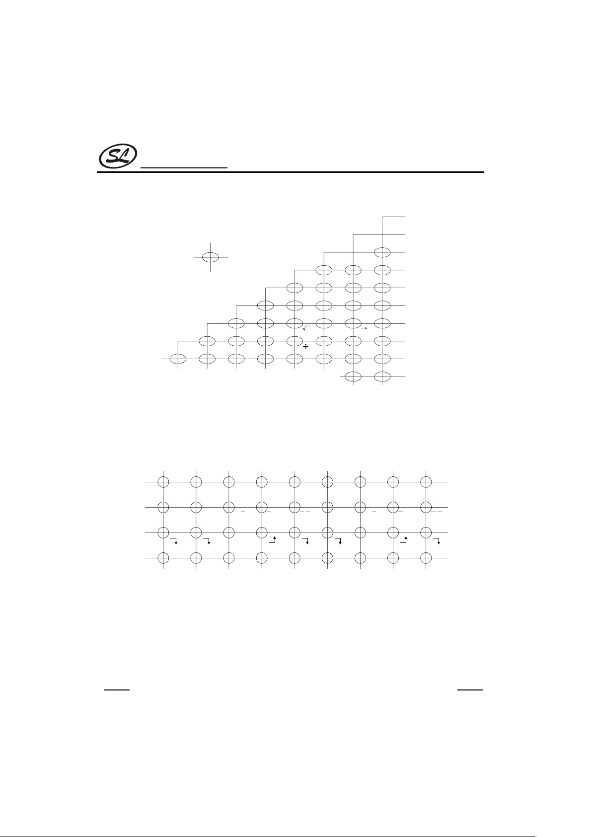
f).Key Definition
i).Touch Key Constitution
OFF
GT+
6
M+
CE
+
.
C
ON
GT-
7
M-
-
00
CE/C
ON
8
IC
X
R
C
GT
R
C
M
01
RM
9
CM
+/-
=
23
%
EX
MU
45
AC
RESET
GND
K1
K2
K3
K4
K5
K6
K7
K8
K9
K10
ii).Lock Key Constitution
10-digit
MH,GTK
10-digit
MH,GTH
12-digit
MH,GTK
12-digit
MH,GTH
10-digit
MK,GTK
10-digit
MK,GTH
12-digit
MK,GTK
12-digit
MK,GTH
A,
A,
A,
A,
A,
A,
A,
A,
5/4 5/4
10ADD432FF 6
OPEN B3 A3 C2 B2 A2 C1 B1 A1
K14
K13
K12
K11
K14: Select withCalculated Digits and Memory Hold Status, MH (Memory Hold), MK (Memory Kill), GTH
(GT Memory Hold) and GTX (GT Memory Kill) at Auto Power OFF or OFF key.
K13: Select withAuto PowerOFF mode and Total switch.
K12: Rounding switches.
K11: Select with Fixed point or Floating mode.
Page 7

Silan
Semiconductors
SC3414
HANGZHOU SILAN MICROELECTRONICS JOINT-STOCK CO.,LTD
Rev: 1.0 2000.12.31
7
B). Keyboard Description
a).Equal Key (=)
i).Performs Keyed-in operation and maintains that operation for possible use.
ii).Establishes power/reciprocation calculation.
b).Multiplication Key (×)
i).Enters multiplicand.
ii).Performs previous operation and displays result.
c).Division Key (H)
i).Enters dividend.
ii).Performs previous operation and displays result.
d).Addition Key (+)
i).Conditions machine for an addition.
ii).Performs previous operation and displays result.
e).Subtraction Key (-)
i).Conditions machine for a subtraction.
ii).Performs previous operation and displays result.
f).Percent Key (%)
The purpose of the percent key is to allow for calculation of add-on and discount. Determination of add-on
requires the principal amount to be the first entry followed by the "+" or "X" key, with the percentage being the
second entry. Depression of the percent key yields the amountto add on, such as tax or interest. Depression of
the "=" keyadds this amount to the principal.
g).Change Sign Key (+/-)
Pushing the "+/-" key twice in succession causes the corresponding sign to appear and disappear. During digit
entry, this function changes he sign of the entered factor.
h).Power On/All Clear Key (ON/AC)
i).First push power-ondisplays "0".
ii).In the middle of a digit entry, a second push will clear all operating register).
i)Clear Entry/Clear Key (CE/C)
i).During the digit entry,the first depression will clear the entry register.And display the previous enter number
again.
ii).The second push will clear all registers.
j).Clear Entry Key (CE)
During the digit entry will clear the entry register and display number "0".
k).Square Root Key (Ö )
Extracts the square root of a positive number displayed in the entry register.
l).Memory Plus Key (M+)
i). Adds the current display to the contents of memory.
ii). It willterminate a number entry.
Page 8

Silan
Semiconductors
SC3414
HANGZHOU SILAN MICROELECTRONICS JOINT-STOCK CO.,LTD
Rev: 1.0 2000.12.31
8
m).Memory Minus Key (M-)
i).Subtracts the current display from the contents of memory
ii).It will terminate a number entry.
n).memory Recall and Clear Key (RCM)
i).First push, as RM key, transfers the contents of the memory register into the display register.
ii).Second push, as CM key, clears the memory.
o).Number, Decimal Key ("00", "0 - 9", "•")
The first number key in a sequence will clear the display and enter the digit in the display. Successive entries
will shift the display left and enters the data in display register. The first decimal point entered is effective. An
attempted entry of more than 12 digits or 11decimal places will be ignored.
p).GT Memory Recall and Clear Key (RC GT)
i).First push, as RGT key, transfers the contents of the GT memory register into the display register.
ii).Second push, as CGT key, clears the GT memory.
q).Exchange Key (EX)
Exchange two operand between the operator. For example, key in "a-b", and then key in "EX" will exchange a
andbto"b-a".
r).Shift Key (→)
Delete the rightest digit and others will shift to right.
s).Item Counter Key (IC)
i).The "+" and "=" key will increase the counter's contents by one.
ii).The "-" will decrease it by two.
iii).The others operator key and number key will not change it.
t).Grand Total Plus(GT+)
Ands the current display to the content of grand total memory.
u).Grand Total Minus (GT-)
Subtracts the current display from the content of grand total memory.
GT- will terminate a number entry.
C). Error Conditions
a).Error Detection
System errors occur when :
i).The integral part of any calculation result exceeds 12 digits.
ii).The integral part of any memory calculation result exceeds 12-digit or when the integral part of any addend
or subtrahend to memory exceeds 12-digit.
iii).The integral part of a mark-up and mark-down calculation result exceeds 12-digit.
v).A division by zero is attempted.
iv).An extraction of the square root of a negative number is attempted.
Page 9
Silan
Semiconductors
SC3414
HANGZHOU SILAN MICROELECTRONICS JOINT-STOCK CO.,LTD
Rev: 1.0 2000.12.31
9
b).Error Indication
i).System error :
a)."0" is indicated in the first-digit position and "E" in the sign-digit position.
b).The high-order 12-digit of a calculation result is indicated together with "E". The location of the decimal
point corresponds to the result of calculation times le-12, and no zero shift is performed.
c).Error Release
i).System error :
A system error can be released by depressing ON/AC key or CE/C key. However the calculation result is
not cleared by CE/C key but is retained.
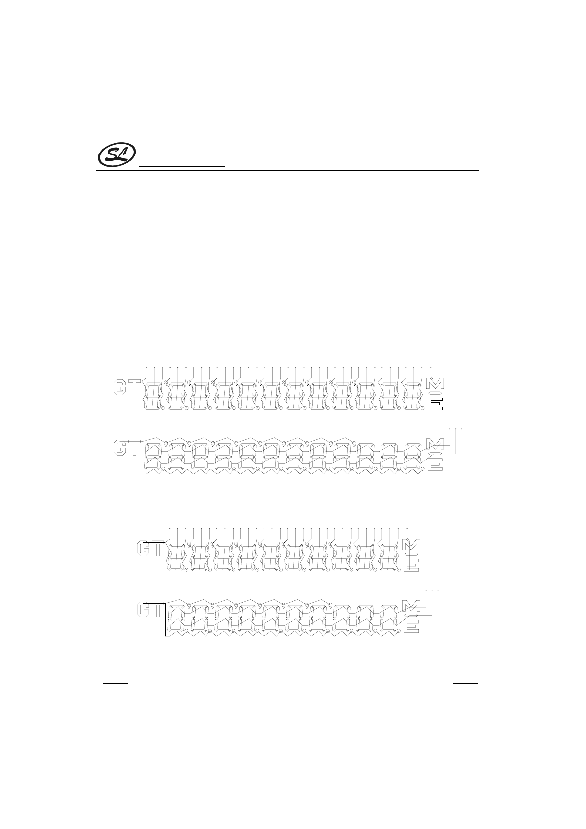
D). LCD Display
a).Inter Connection of LCD
i).Select of 10-digits
C8 B8 A8 C7 B7 A7 C6 B6 A6 C5 B5 A5 C4 B4 A4 C3 B3 A3 C2 B2 A2 C1 B1 A1
S1
COM 1 23
SEGMENT
COMMON
C9 B9 A9C12 B12 A12C11 B11A11C10 B10 A10
ii).Select of 12-digits
C10 B10 A10 C9 B9 A9 C8 B8 A8 C7 B7 A7 C6 B6 A6 C5 B5 A5 C4 B4 A4 C3 B3 A3 C2 B2 A2 C1 B1 A1
S1
COM 1 23
SEGMENT
COMMON
Page 10
Silan
Semiconductors
SC3414
HANGZHOU SILAN MICROELECTRONICS JOINT-STOCK CO.,LTD
Rev: 1.0 2000.12.31
10
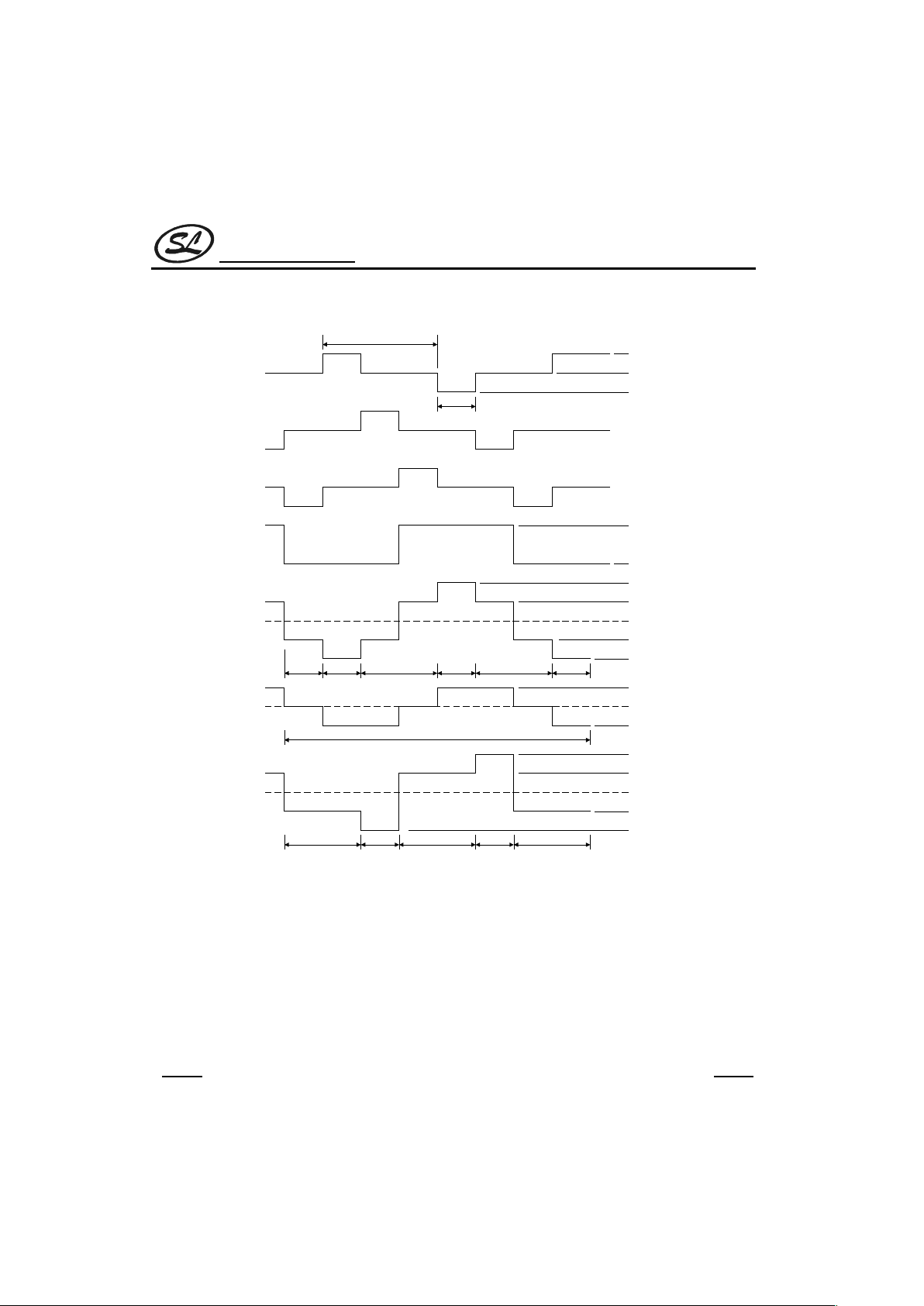
E). Waveforms for Display
VEE=3V
V
DD
=1.5V
GND
V
EE
=3V
GND
+3.0V
+1.5V
0V
-1.5V
-3.0V
+1.5V
0V
-1.5V
+3.0V
+1.5V
0V
-1.5V
-3.0V
T
T1
OFF ON OFF ON OFF ON
OFF
OFF ON OFF ON OFF
When f0=18kHz
T=1/93.8Hz T1=3.56ms
COM3
COM1
COM2
SEGMENT
A1
A1-COM3
(ON)
A1-COM2
(OFF)
A1-COM1
(ON)
Page 11
Silan
Semiconductors
SC3414
HANGZHOU SILAN MICROELECTRONICS JOINT-STOCK CO.,LTD
Rev: 1.0 2000.12.31
11
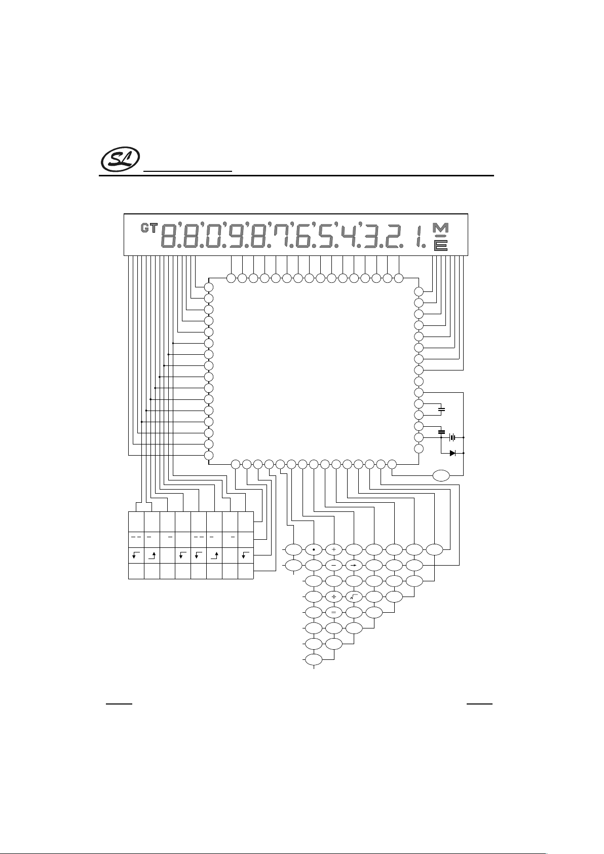
APPLICATION CIRCUITS
C
ON
A3
B3
C3
A4
B4
C4
A5
COM3
A1
B1
C1
A2
B2
C2
COM1
COM2
C12
B12
A12
C11
B11
A11
C10
VDD
VEE
VB
VA
GND
S2
S1
TS1
B7
A7
C6
C6
A6
C5
B5
C9
B9
A9
C8
B8
A8
C7
B10
A10
K8
K9
K10
K11
K12
K13
K14
K1
K2
K3
K4
K5
K6
K7
RESET
SC3414
12
MK
GTH
A,
ADD
12
MK
GTK
A,
0
10
MK
GTH
A,
1
10
MK
GTK
A,
2
12
MH
GTH
A,
3
12
MH
GTK
A,
4
10
MH
GTH
A,
6
10
MH
GTK
A,
F
5/4 5/4
AC
CE M+ 6 GT+ OFF
C/CE
ON
00 M- 7 GT-
0
X
IC 8
1 RM 9
2 +/- CM
3 % EX
4 MU
5
R
C
GT
R
C
M
Page 12
Silan
Semiconductors
SC3414
HANGZHOU SILAN MICROELECTRONICS JOINT-STOCK CO.,LTD
Rev: 1.0 2000.12.31
12
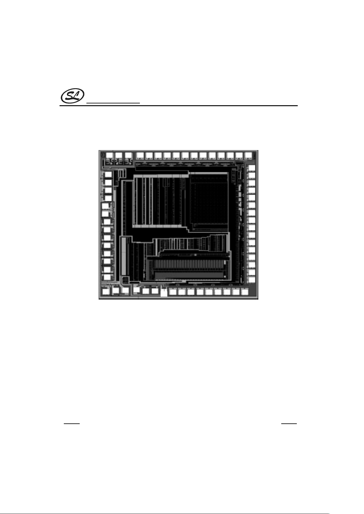
CHIP TOPOGRAPHY
50 49 48 47 46 45 44 43 42 41 40 39 38 37 36 35
34
33
32
31
30
29
28
27
26
25
24
23
22
21
20
18
17161514131211109
9
8
76
5
43
2
1
64
63
62
61
60
59
58
57
56
55
54
53
52
K1
K2
K4
K3
K5
K6
K7
K8
K9
K10
K11
K12
K13
K14
COM1
COM2
COM3A1B1
C1
A2
B2
C2
A3
B3
C3
A4
B4
C4
A5
B5
C5
A6
B6
C6
A7
B7
C7
A8
B8
C8
A9
B9
C9
A10
B10
C10
A11
B11
C11
A12
B12
C12
S1
S2
GND
VA
VB
VEE
VDD
TS1
RESET
Chip Size : 2.780 x 2.510 (mm2)
Page 13
Silan
Semiconductors
SC3414
HANGZHOU SILAN MICROELECTRONICS JOINT-STOCK CO.,LTD
Rev: 1.0 2000.12.31
13
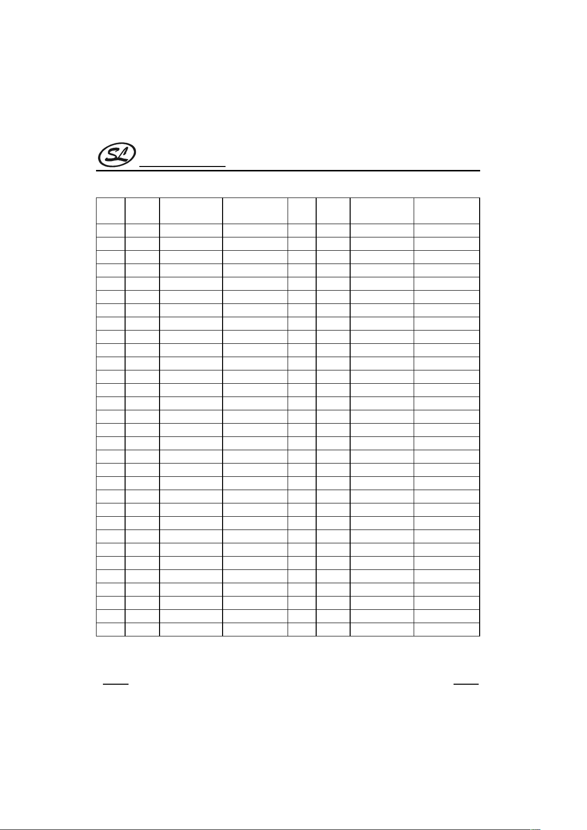
PAD COORDINATES
(Unit: µm)
Pin
No.
Symbol X Y
Pin
No.
Symbol X Y
1K1
-1065 -995
33 C5
1100 875
2 RESET
-1085 -1230
34 B5
1100 1010
3TS1
-940 -1205
35 A5
1050 1240
4VDD
-790 -1200
36 C4
920 1240
5 VEE
-625 -1200
37 B4
780 1240
6VB
-490 -1220
38 A4
645 1240
7VA
-350 -1215
39 C3
510 1240
8GND
-215 -1230
40 B3
375 1240
9S2
-80 -1235
41 A3
240 1240
10 S1
55 -1235
42 C2
105 1240
11 C12
190 -1235
43 B2
-30 1240
12 B12
325 -1235
44 A2
-165 1240
13 A12
460 -1235
45 C1
-300 1240
14 C11
595 -1235
46 B1
-435 1240
15 B11
730 -1235
47 A1
-570 1240
16 A11
865 -1235
48 COM3
-750 1240
17 C10
1000 -1235
49 COM2
-890 1240
18 B10
1100 -1015
50 COM1
-1030 1240
20 A10
1100 -880
52 K14
-1050 895
21 C9
1100 -745
53 K13
-1050 745
22 B9
1100 -610
54 K12
-1050 605
23 A9
1100 -475
55 K11
-1050 455
24 C8
1100 -340
56 K10
-1100 320
25 B8
1100 -205
57 K9 -1100 175
26 A8
1100 -70
58 K8 -1065 35
27 C7
1100 65
59 K7 -1065 -110
28 B7
1100 200
60 K6 -1065 -255
29 A7
1100 335
61 K5 -1065 -390
30 C6
1100 470
62 K4 -1065 -545
31 B6
1100 605
63 K3 -1065 -675
32 A6
1100 740
64 K2 -1065 -830
Note: The original point of the coordinate is the die center.
 Loading...