

Page 1

INTEGRATED CIRCUITS
SC28L92
Dual Universal Asynchronous
Receiver/Transmitter (DUART)
Preliminary specification
IC19 Data Handbook
1998 Oct 05
Page 2

Philips Semiconductors Preliminary specification
Dual Universal Asynchronous
Receiver/Transmitter (DUART)
DESCRIPTION
The SC28L92 is a pin and function replacement for the SCC2692
and SC26C92 operating at 3.3 or 5 volts supply with added features
and deeper FIFOs. Its configuration on power up is that of the 2692.
Its differences from the 2692 are: 16 character receiver, 16
character transmit FIFOs, watch dog timer for each receiver, mode
register 0 is added, extended baud rate and overall faster speeds,
programmable receiver and transmitter interrupts. (Neither the
SC26C92 nor The SCC2692 is being discontinued.)
Pin programming will allow the device to operate with either the
Motorola or Intel bus interface The bit 3 of the MR0a register allows
the device to operate in an 8 byte FIFO mode if strict compliance
with the SC26C92 FIFO structure is required
The Philips Semiconductors SC28L92 Dual Universal Asynchronous
Receiver/Transmitter (DUART) is a single-chip CMOS-LSI
communications device that provides two full-duplex asynchronous
receiver/transmitter channels in a single package. It interfaces
directly with microprocessors and may be used in a polled or
interrupt driven system.
The operating mode and data format of each channel can be
programmed independently. Additionally , each receiver and
transmitter can select its operating speed as one of eighteen fixed
baud rates; a 16X clock derived from a programmable counter/timer,
or an external 1X or 16X clock. The baud rate generator and
counter/timer can operate directly from a crystal or from external
clock inputs. The ability to independently program the operating
speed of the receiver and transmitter make the DUART particularly
attractive for dual-speed channel applications such as clustered
terminal systems.
Each receiver and transmitter is buffered by 8 or 16 character FIFOs
to minimize the potential of receiver overrun, transmitter underpin
and to reduce interrupt overhead in interrupt driven systems. In
addition, a flow control capability is provided to disable a remote
transmitter when the receiver buffer is full.
Also provided on the SC28L92 are a multipurpose 7-bit input port
and a multipurpose 8-bit output port. These can be used as general
purpose I/O ports or can be assigned specific functions (such as
clock inputs or status/interrupt outputs) under program control.
The SC28L92 is available in two package versions: a 44-pin PLCC
and 44-pin plastic quad flat pack (PQFP).
FEATURES
•3.3 or 5.0 volt operation
•Dual full-duplex independent asynchronous receiver/transmitters
•16 character FIFOs for each receiver and transmitter
•Pin programming for 68K or 80xxx bus interface
•Programmable data format
– 5 to 8 data bits plus parity
– Odd, even, no parity or force parity
SC28L92
– - 1, 1.5 or 2 stop bits programmable in 1/16-bit increments
•16-bit programmable Counter/Timer
•Programmable baud rate for each receiver and transmitter
selectable from:
– 23 fixed rates: 50 to 230.4k baud
– Other baud rates to MHz at 16X
– Programmable user-defined rates derived from a programmable
counter/timer
– External 1X or 16X clock
•Parity, framing, and overrun error detection
•False start bit detection
•Line break detection and generation
•Programmable channel mode
– Normal (full-duplex)
– Automatic echo
– Local loop back
– Remote loop back
– Multi-drop mode (also called ‘wake-up’ or ‘9-bit’)
•Multi-function 7-bit input port
– Can serve as clock or control inputs
– Change of state detection on four inputs
– Inputs have typically >100k pull-up resistors
•Multi-function 8-bit output port
– Individual bit set/reset capability
– Outputs can be programmed to be status/interrupt signals
•Versatile interrupt system
– Single interrupt output with eight maskable interrupting
conditions
– Output port can be configured to provide a total of up to six
separate interrupt outputs that may be wire ORed.
– Each FIFO can be programmed for four different interrupt levels
– Watch dog timer for each receiver
•Maximum data transfer rates:
1X – 1Mb/sec, 16X – 1Mb/sec
•Automatic wake-up mode for multi-drop applications
•Start-end break interrupt/status
•Detects break which originates in the middle of a character
•On-chip crystal oscillator
•Power down mode
•Receiver time-out mode
•Single +3.3V or +5V power supply
•Powers up to emulate SCC2692 and S26C92
1998 Oct 05
2
Page 3
Philips Semiconductors Preliminary specification
Dual Universal Asynchronous
Receiver/Transmitter (DUART)
ORDERING INFORMATION
DESCRIPTION
44-Pin Plastic Leaded Chip Carrier (PLCC)
44-Pin Plastic Quad Flat Pack (PQFP)
INDUSTRIAL
VCC = +3.3 +5V ±10%,
TA = –40 to +85°C
SC28L92A1A
SC28L92A1B
SC28L92
DRAWING NUMBER
SOT187–2
SOT307-2
1998 Oct 05
3
Page 4

Philips Semiconductors Preliminary specification
Dual Universal Asynchronous
Receiver/Transmitter (DUART)
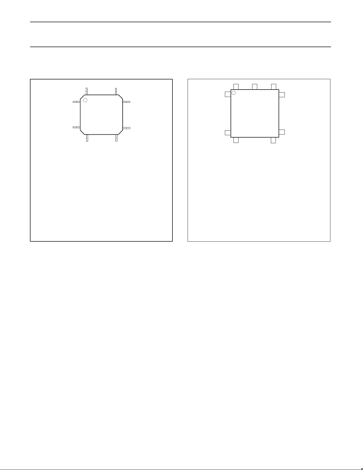
PIN CONFIGURATION DIAGRAM 80XXX PIN CONFIGURA TION
44 34
1
PQFP
11
12 22
Pin Function
1A3
2 IP0
3 WRN
4 RDN
5 RxDB
6 TxDB
7 OP1
8 OP3
9 OP5
10 OP7
11 I/M
12 D1
13 D3
14 D5
15 D7
Pin Function
16 GND
17 GND
18 INTRN
19 D6
20 D4
21 D2
22 D0
23 NC
24 OP6
25 OP4
26 OP2
27 OP0
28 TxDA
29 RxDA
30 x1/clk
Pin Function
31 x2
32 RESET
33 CEN
34 IP2
35 IP6
36 IP5
37 IP4
38 V
39 V
40 A0
41 IP3
42 A1
43 IP1
44 A2
SC28L92
6
7
33
23
Pin Function
1NC
2A0
3 IP3
4A1
5 IP1
6A2
CC
CC
SD00671
7A3
8 IP0
9 WRN
10 RDN
11 RxDB
12 I/M
13 TxDB
14 OP1
15 OP3
17
18
1
PLCC
Pin Function
16 OP5
17 OP7
18 D1
19 D3
20 D5
21 D7
22 V
23 NC
24 INTRN
25 D6
26 D4
27 D2
28 D0
29 OP6
30 OP4
40
39
29
28
Pin Function
31 OP2
32 OP0
33 TxDA
34 NC
35 RxDA
36 X1/CLK
SS
37 X2
38 RESET
39 CEN
40 IP2
41 IP6
42 IP5
43 IP4
44 V
CC
SD00672
1998 Oct 05
4
Page 5
Philips Semiconductors Preliminary specification
Dual Universal Asynchronous
Receiver/Transmitter (DUART)
PIN CONFIGURATION DIAGRAM 68XXX PIN CONFIGURA TION
44 34
1
PQFP
11
12 22
Pin Function
1A3
2 IP0
3 R/WN
4 DACKN
5 RxDB
6 TxDB
7 OP1
8 OP3
9 OP5
10 OP7
11 I/M
12 D1
13 D3
14 D5
15 D7
Pin Function
16 GND
17 GND
18 INTRN
19 D6
20 D4
21 D2
22 D0
23 NC
24 OP6
25 OP4
26 OP2
27 OP0
28 TxDA
29 RxDA
30 x1/clk
Pin Function
31 x2
32 RESETN
33 CSN
34 IP2
35 IACKN
36 IP5
37 IP4
38 V
39 V
40 A0
41 IP3
42 A1
43 IP1
44 A2
SC28L92
6
7
33
23
Pin Function
1NC
2A0
3 IP3
4A1
5 IP1
6A2
CC
CC
SD00673
7A3
8 IP0
9 R/WN
10 DACKN
11 RxDB
12 I/M
13 TxDB
14 OP1
15 OP3
17
18
1
PLCC
Pin Function
16 OP5
17 OP7
18 D1
19 D3
20 D5
21 D7
22 V
23 NC
24 INTRN
25 D6
26 D4
27 D2
28 D0
29 OP6
30 OP4
40
39
29
28
Pin Function
31 OP2
32 OP0
33 TxDA
34 NC
35 RxDA
36 X1/CLK
SS
37 X2
38 RESETN
39 CEN
40 IP2
41 IACKN
42 IP5
43 IP4
44 V
CC
SD00674
1998 Oct 05
5
Page 6
Philips Semiconductors Preliminary specification
Dual Universal Asynchronous
Receiver/Transmitter (DUART)
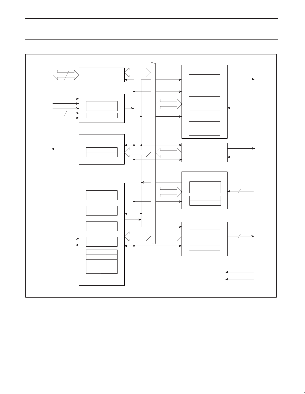
8
D0–D7
RDN
WRN
CEN
A0–A3
RESET
INTRN
4
BUS BUFFER
OPERATION CONTROL
ADDRESS
DECODE
R/W CONTROL
INTERRUPT CONTROL
IMR
ISR
CHANNEL A
8 BYTE TRANSMIT
FIFO
TRANSMIT
SHIFT REGISTER
8 BYTE RECEIVE
FIFO
WATCH DOG TIMER
RECEIVE SHIFT
REGISTER
MRA0, 1, 2
CRA
SRA
CHANNEL B
(AS ABOVE)
SC28L92
TxDA
RxDA
TxDB
RxDB
X1/CLK
INPUT PORT
TIMING
BAUD RATE
GENERATOR
CLOCK
SELECTORS
COUNTER/
TIMER
X2
XTAL OSC
CSRA
CSRB
ACR
U
CTPL
CTPL
CONTROL
TIMING
INTERNAL DATABUS
CHANGE OF
STATE
DETECTORS (4)
IPCR
ACR
OUTPUT PORT
FUNCTION
SELECT LOGIC
OPCR
OPR
7
8
IP0-IP6
OP0-OP7
V
CC
V
SS
SD00153
Figure 1. Block Diagram
1998 Oct 05
6
Page 7
Philips Semiconductors Preliminary specification
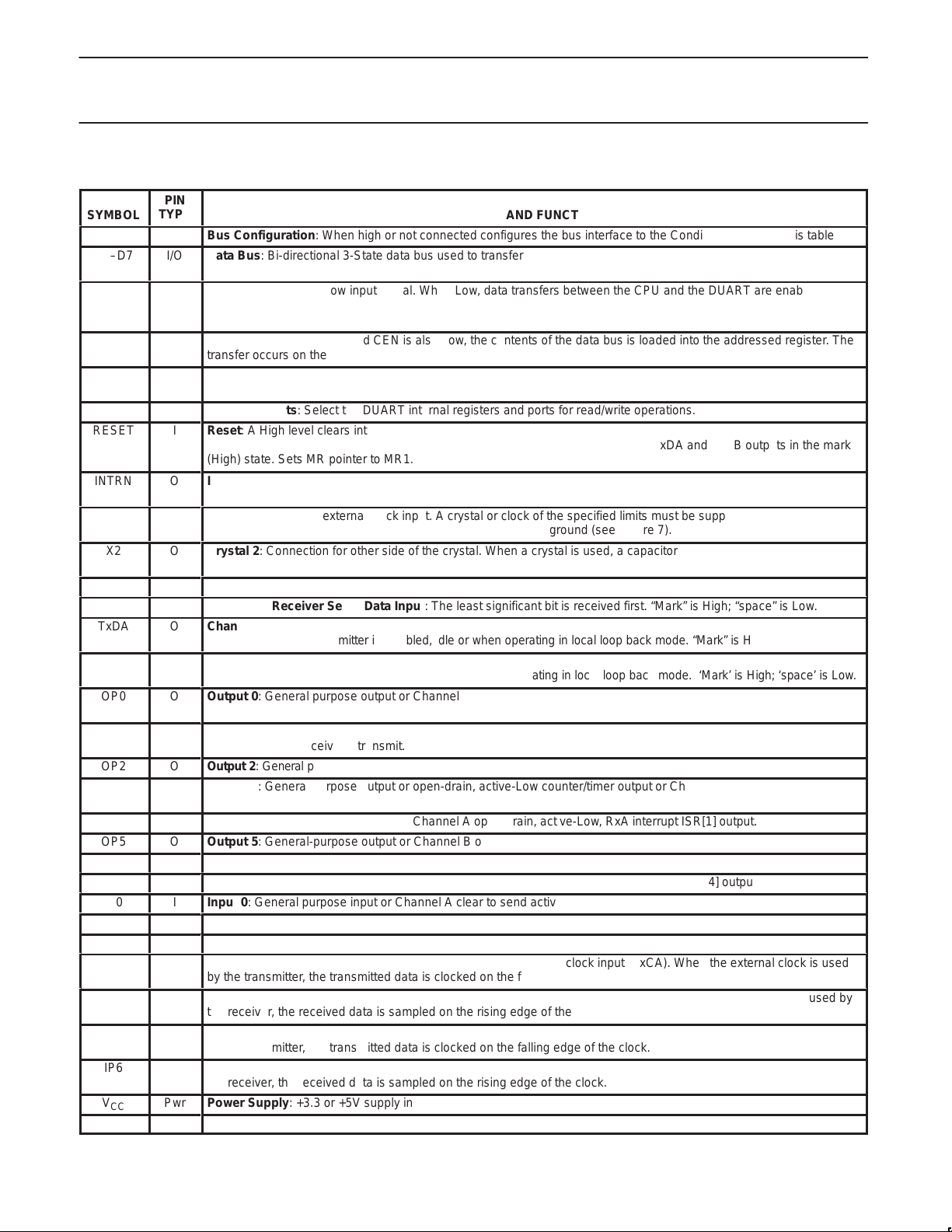
Á
Á
Á
Á
Á
Á
Á
Á
Á
Á
Á
Á
Á
Á
Á
Á
Á
Á
Á
Á
Á
Á
Á
Á
Á
Á
Á
Á
Á
Á
Á
Á
Á
Dual Universal Asynchronous
Receiver/Transmitter (DUART)
PIN CONFIGURATION FOR 80XXX BUS INTERFACE (INTEL)
ÁÁ
SYMBOL
I/M
D0–D7
CEN
ÁÁ
WRN
ÁÁ
RDN
A0–A3
RESET
ÁÁ
INTRN
ÁÁ
X1/CLK
X2
ÁÁ
RxDA
RxDB
TxDA
ÁÁ
TxDB
OP0
ÁÁ
OP1
OP2
OP3
ÁÁ
OP4
OP5
OP6
OP7
IP0
IP1
IP2
IP3
ÁÁ
IP4
IP5
ÁÁ
IP6
V
CC
GND
PIN
Á
TYPE
I
I/O
I
Á
I
Á
I
I
I
Á
O
Á
I
O
Á
I
I
O
Á
O
O
Á
O
O
O
Á
O
O
O
O
I
I
I
I
Á
I
I
Á
I
Pwr
Pwr
БББББББББББББББББББББББББББ
NAME AND FUNCTION
Bus Configuration: When high or not connected configures the bus interface to the Conditions shown in this table.
Data Bus: Bi-directional 3-State data bus used to transfer commands, data and status between the DUART and the
CPU. D0 is the least significant bit.
Chip Enable: Active-Low input signal. When Low, data transfers between the CPU and the DUART are enabled on
D0–D7 as controlled by the WRN, RDN and A0–A3 inputs. When High, places the D0–D7 lines in the 3-State
БББББББББББББББББББББББББББ
condition.
Write Strobe: When Low and CEN is also Low, the contents of the data bus is loaded into the addressed register. The
БББББББББББББББББББББББББББ
transfer occurs on the rising edge of the signal.
Read Strobe: When Low and CEN is also Low, causes the contents of the addressed register to be presented on the
data bus. The read cycle begins on the falling edge of RDN.
Address Inputs: Select the DUART internal registers and ports for read/write operations.
Reset: A High level clears internal registers (SRA, SRB, IMR, ISR, OPR, OPCR), puts OP0–OP7 in the High state,
stops the counter/timer, and puts Channels A and B in the inactive state, with the TxDA and TxDB outputs in the mark
БББББББББББББББББББББББББББ
(High) state. Sets MR pointer to MR1.
Interrupt Request: Active-Low, open-drain, output which signals the CPU that one or more of the eight maskable
interrupting conditions are true.
БББББББББББББББББББББББББББ
Crystal 1: Crystal or external clock input. A crystal or clock of the specified limits must be supplied at all times. When a
crystal is used, a capacitor must be connected from this pin to ground (see Figure 7).
Crystal 2: Connection for other side of the crystal. When a crystal is used, a capacitor must be connected from this pin
to ground (see Figure 7). If X1/CLK is driven from an external source, this pin must be left open.
БББББББББББББББББББББББББББ
Channel A Receiver Serial Data Input: The least significant bit is received first. “Mark” is High; “space” is Low.
Channel B Receiver Serial Data Input: The least significant bit is received first. “Mark” is High; “space” is Low.
Channel A Transmitter Serial Data Output: The least significant bit is transmitted first. This output is held in the “mark”
БББББББББББББББББББББББББББ
condition when the transmitter is disabled, idle or when operating in local loop back mode. “Mark” is High; “space” is Low.
Channel B Transmitter Serial Data Output: The least significant bit is transmitted first. This output is held in the ‘mark’
condition when the transmitter is disabled, idle, or when operating in local loop back mode. ‘Mark’ is High; ‘space’ is Low.
Output 0: General purpose output or Channel A request to send (RTSAN, active-Low). Can be deactivated
automatically on receive or transmit.
БББББББББББББББББББББББББББ
Output 1: General-purpose output or Channel B request to send (RTSBN, active-Low). Can be deactivated
automatically on receive or transmit.
Output 2: General purpose output, or Channel A transmitter 1X or 16X clock output, or Channel A receiver 1X clock output.
Output 3: General purpose output or open-drain, active-Low counter/timer output or Channel B transmitter 1X clock
output, or Channel B receiver 1X clock output.
БББББББББББББББББББББББББББ
Output 4: General purpose output or Channel A open-drain, active-Low, RxA interrupt ISR[1] output.
Output 5: General-purpose output or Channel B open-drain, active-Low, RxB interrupt ISR[5] output.
Output 6: General purpose output or Channel A open-drain, active-Low, TxA interrupt ISR[0] output.
Output 7: General-purpose output, or Channel B open-drain, active-Low, TxB interrupt ISR[4] output.
Input 0: General purpose input or Channel A clear to send active-Low input (CTSAN).
Input 1: General purpose input or Channel B clear to send active-Low input (CTSBN).
Input 2: General-purpose input or counter/timer external clock input.
Input 3: General purpose input or Channel A transmitter external clock input (TxCA). When the external clock is used
БББББББББББББББББББББББББББ
by the transmitter, the transmitted data is clocked on the falling edge of the clock.
Input 4: General purpose input or Channel A receiver external clock input (RxCA). When the external clock is used by
the receiver, the received data is sampled on the rising edge of the clock.
Input 5: General purpose input or Channel B transmitter external clock input (TxCB). When the external clock is used
БББББББББББББББББББББББББББ
by the transmitter, the transmitted data is clocked on the falling edge of the clock.
Input 6: General purpose input or Channel B receiver external clock input (RxCB). When the external clock is used by
the receiver, the received data is sampled on the rising edge of the clock.
Power Supply: +3.3 or +5V supply input ±10%
Ground
SC28L92
1998 Oct 05
7
Page 8
Philips Semiconductors Preliminary specification
Á
Á
Á
Á
Á
Á
Á
Á
Á
Á
Á
Á
Á
Á
Á
Á
Á
Á
Á
Á
Á
Á
Á
Á
Á
Á
Á
Á
Á
Á
Dual Universal Asynchronous
Receiver/Transmitter (DUART)
PIN CONFIGURATION FOR 68XXX BUS INTERFACE (MOTOROLA)
ÁÁ
SYMBOL
I/M
D0–D7
CSN
ÁÁ
R/WN
IACKN
DACKN
ÁÁ
A0–A3
RESETN
ÁÁ
INTRN
X1/CLK
ÁÁ
X2
RxDA
RxDB
TxDA
ÁÁ
TxDB
OP0
ÁÁ
OP1
OP2
ÁÁ
OP3
OP4
OP5
OP6
OP7
IP0
IP1
IP2
IP3
ÁÁ
IP4
IP5
ÁÁ
V
CC
GND
PIN
Á
TYPE
I
I/O
I
Á
I
I
O
Á
I
I
Á
O
I
Á
O
I
I
O
Á
O
O
Á
O
O
Á
O
O
O
O
O
I
I
I
I
Á
I
I
Á
Pwr
Pwr
БББББББББББББББББББББББББББ
NAME AND FUNCTION
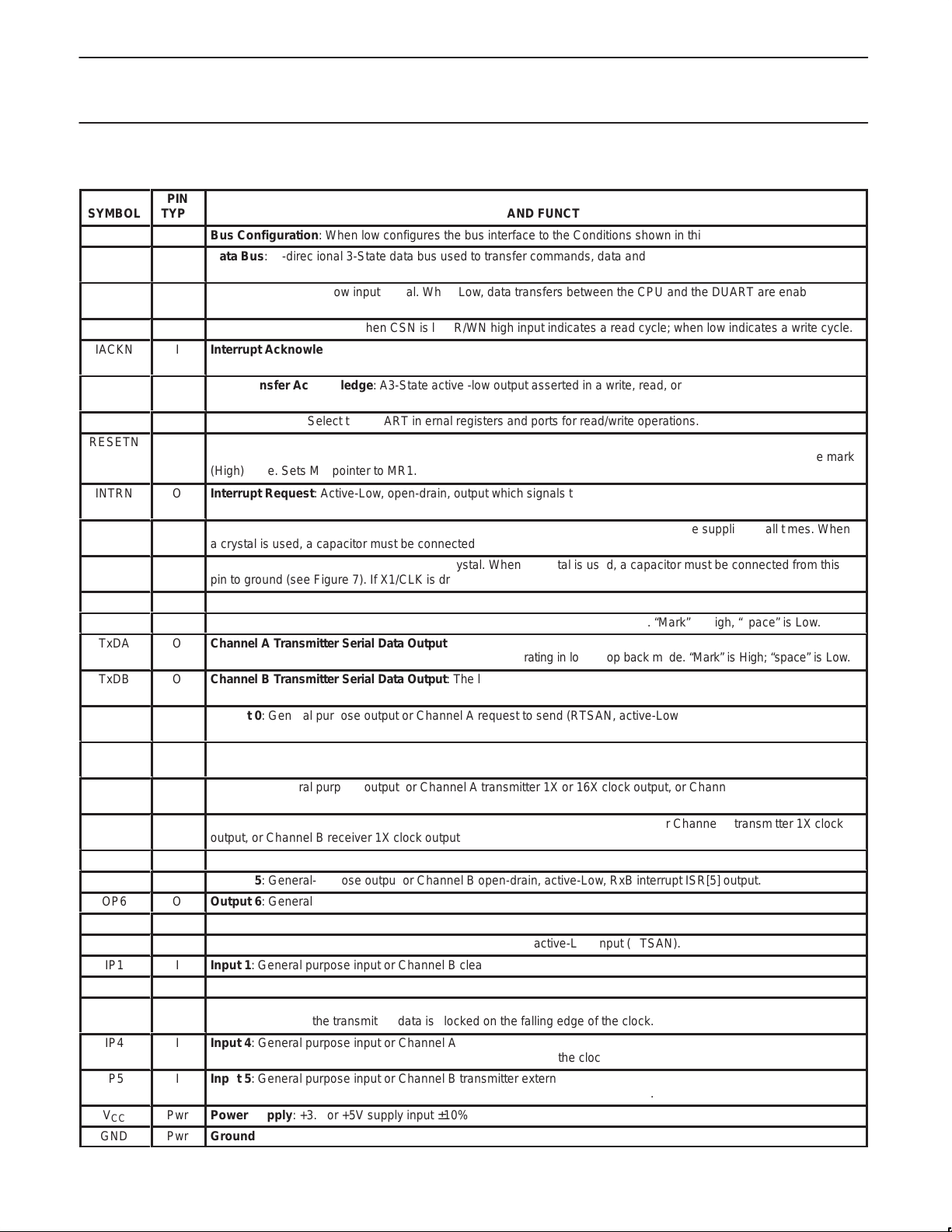
Bus Configuration: When low configures the bus interface to the Conditions shown in this table.
Data Bus: Bi-directional 3-State data bus used to transfer commands, data and status between the DUART and the
CPU. D0 is the least significant bit.
Chip Enable: Active-Low input signal. When Low, data transfers between the CPU and the DUART are enabled on
БББББББББББББББББББББББББББ
D0–D7 as controlled by the R/WN and A0–A3 inputs. When High, places the D0–D7 lines in the 3-State condition.
Read/Write: Input Signal. When CSN is low R/WN high input indicates a read cycle; when low indicates a write cycle.
Interrupt Acknowledge: Active low input indicating an interrupt acknowledge cycle. Usually asserted by the CPU in
response to an interrupt request. When asserted places the interrupt vector on the bus and asserts DACKN.
Data Transfer Acknowledge: A3-State active -low output asserted in a write, read, or interrupt acknowledge cycle to
indicate proper transfer of data between the CPU and the DUART.
БББББББББББББББББББББББББББ
Address Inputs: Select the DUART internal registers and ports for read/write operations.
Reset: A low level clears internal registers (SRA, SRB, IMR, ISR, OPR, OPCR), puts OP0–OP7 in the High state,
stops the counter/timer, and puts Channels A and B in the inactive state, with the TxDA and TxDB outputs in the mark
(High) state. Sets MR pointer to MR1.
БББББББББББББББББББББББББББ
Interrupt Request: Active-Low, open-drain, output which signals the CPU that one or more of the eight maskable
interrupting conditions are true.
Crystal 1: Crystal or external clock input. A crystal or clock of the specified limits must be supplied at all times. When
a crystal is used, a capacitor must be connected from this pin to ground (see Figure 7).
БББББББББББББББББББББББББББ
Crystal 2: Connection for other side of the crystal. When a crystal is used, a capacitor must be connected from this
pin to ground (see Figure 7). If X1/CLK is driven from an external source, this pin must be left open.
Channel A Receiver Serial Data Input: The least significant bit is received first. “Mark” is High, “space” is Low.
Channel B Receiver Serial Data Input: The least significant bit is received first. “Mark” is High, “space” is Low.
Channel A Transmitter Serial Data Output: The least significant bit is transmitted first. This output is held in the “mark”
condition when the transmitter is disabled, idle or when operating in local loop back mode. “Mark” is High; “space” is Low.
БББББББББББББББББББББББББББ
Channel B Transmitter Serial Data Output: The least significant bit is transmitted first. This output is held in the ‘mark’
condition when the transmitter is disabled, idle, or when operating in local loop back mode. ‘Mark’ is High; ‘space’ is Low.
Output 0: General purpose output or Channel A request to send (RTSAN, active-Low). Can be deactivated
automatically on receive or transmit.
БББББББББББББББББББББББББББ
Output 1: General-purpose output or Channel B request to send (RTSBN, active-Low). Can be deactivated
automatically on receive or transmit.
Output 2: General purpose output, or Channel A transmitter 1X or 16X clock output, or Channel A receiver 1X clock
output.
БББББББББББББББББББББББББББ
Output 3: General purpose output or open-drain, active-Low counter/timer output or Channel B transmitter 1X clock
output, or Channel B receiver 1X clock output.
Output 4: General purpose output or Channel A open-drain, active-Low, RxA interrupt ISR [1] output.
Output 5: General-purpose output or Channel B open-drain, active-Low, RxB interrupt ISR[5] output.
Output 6: General purpose output or Channel A open-drain, active-Low, TxA interrupt ISR[0] output.
Output 7: General-purpose output, or Channel B open-drain, active-Low, TxB interrupt ISR[4] output.
Input 0: General purpose input or Channel A clear to send active-Low input (CTSAN).
Input 1: General purpose input or Channel B clear to send active-Low input (CTSBN).
Input 2: General-purpose input or counter/timer external clock input.
Input 3: General purpose input or Channel A transmitter external clock input (TxCA). When the external clock is used
by the transmitter, the transmitted data is clocked on the falling edge of the clock.
БББББББББББББББББББББББББББ
Input 4: General purpose input or Channel A receiver external clock input (RxCA). When the external clock is used by
the receiver, the received data is sampled on the rising edge of the clock.
Input 5: General purpose input or Channel B transmitter external clock input (TxCB). When the external clock is used
by the transmitter, the transmitted data is clocked on the falling edge of the clock.
БББББББББББББББББББББББББББ
Power Supply: +3.3 or +5V supply input ±10%
Ground
SC28L92
1998 Oct 05
8
Page 9
Philips Semiconductors Preliminary specification
V
VIHIn ut high voltage (exce t X1/CLK)
Dual Universal Asynchronous
Receiver/Transmitter (DUART)
ABSOLUTE MAXIMUM RATINGS
SYMBOL
T
T
V
V
P
P
A
STG
CC
S
D
D
Operating ambient temperature range
Storage temperature range -65 to +150 °C
Voltage from VCC to GND
Voltage from any pin to GND
Package power dissipation (PLCC44) 2.4 W
Package power dissipation (PQFP44) 1.78 W
Derating factor above 25C (PLCC44)
Derating factor above 25C (PQFP44)
NOTES:
1. Stresses above those listed under Absolute Maximum Ratings may cause permanent damage to the device. This is a stress rating only and
functional operation of the device at these or any other condition above those indicated in the operation section of this specification is not
implied.
2. For operating at elevated temperatures, the device must be derated based on +150°C maximum junction temperature.
3. This product includes circuitry specifically designed for the protection of its internal devices from damaging effects of excessive static
charge. Nonetheless, it is suggested that conventional precautions be taken to avoid applying any voltages larger than the rated maxima.
4. Parameters are valid over specified temperature range.
DC ELECTRICAL CHARACTERISTICS
VCC = 5V ± 10%, T
SYMBOL PARAMETER TEST CONDITIONS Min Typ Max UNIT
V
IL
V
IH
V
OL
V
OH
I
IX1PD
I
ILX1
I
IHX1
I
I
I
OZH
I
OZL
I
ODL
I
ODH
I
CC
NOTES:
1. Parameters are valid over specified temperature range.
2. Typical values are at +25°C, typical supply voltages, and typical processing parameters.
3. Test conditions for outputs: C
4. All outputs are disconnected. Inputs are switching between CMOS levels of VCC -0.2V and VSS + 0.2V.
5. See UART application note for power down currents of 5µA or less.
= –40C to 85C, unless otherwise specified.
A
Input low voltage 0.8
p
Input high voltage (X1/CLK) 0.8 V
Output low voltage
Output high voltage (except OD outputs)
X1/CLK input current - power down
X1/CLK input low current - operating
X1/CLK input high current - operating
Input leakage current:
All except input port pins
Input port pins
Output off current high, 3-State data bus
Output off current low , 3-State data bus
Open-drain output low current in off-state
Open-drain output high current in off-state
Power supply current
Operating mode
Power down mode
= 150pF, except interrupt outputs. Test conditions for interrupt outputs: CL = 50pF, R
L
1
PARAMETER RATING UNIT
2
3
3
Note 4 °C
-0.5 to +7.0 V
-0.5 to VCC +0.5 V
19
14
1, 2
LIMITS
p
3
4
5
0 to +70°C 2.4
–40 to +85°C 2.5 V
CC
I
= 2.4mA
OL
= -400µA
I
OH
V
= 0 to V
IN
CC
VIN = 0
V
= V
IN
CC
VIN = 0 to V
VIN = 0 to V
VIN = V
VIN = 0V –1
CC
CC
CC
VIN = 0
V
= V
IN
CC
V
CC
-100
-10
–1
-1
-1
0
-0.5
CMOS input levels
CMOS input levels
2
SC28L92
mW/C
mW/C
0.4 V
+1
0
100
+1
+10
1 µA
1
25
10.0
= 2.7KΩ to VCC.
L
V
V
µA
µA
µA
µA
µA
µA
µA
µA
mA
A
1998 Oct 05
9
Page 10
Philips Semiconductors Preliminary specification
Dual Universal Asynchronous
Receiver/Transmitter (DUART)
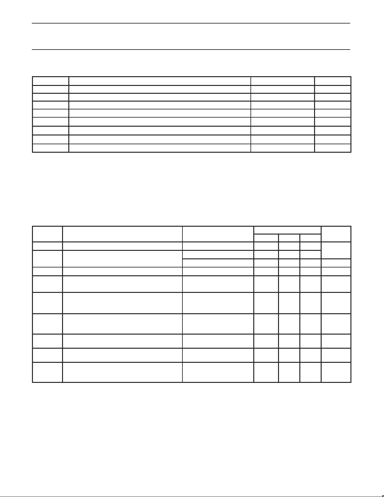
AC CHARACTERISTICS (80XXX MODE)
= 5.0V ± 10%, T
V
CC
SYMBOL
Reset Timing (See Figure 2)
t
RES
Bus Timing5 (See Figure 3)
t
*AS
t
*AH
t
*CS
t
*CH
t
*RW
t
*DD
t
*DA
t
*DF
t
*DI
t
*DS
t
*DH
t
*RWD
Port Timing5 (See Figure 8)
t
*PS
t
*PH
t
*PD
Interrupt Timing (See Figure 10)
t
*IR
Clock Timing (See Figure 7)
t
*CLK
f
*CLK
f
*CTC
f
*CTC
t
*RX
f
*RX
t
*TX
f
*TX
= –40C to 85C, unless otherwise specified.
A
PARAMETER
Reset pulse width
A0–A3 setup time to RDN, WRN Low
A0–A3 hold time from RDN, WRN low
CEN setup time to RDN, WRN low
CEN Hold time from RDN. WRN low
WRN, RDN pulse width (Low time)
Data valid after RDN low
RDN low to data bus active
6
Data bus floating after RDN or CEN high
RDN or CEN high to data bus invalid
Data bus setup time before WRN or CEN high (write cycle)
Data hold time after WRN high
High time between read and/or write cycles
Port in setup time before RDN low (Read IP ports cycle)
Port in hold time after RDN high
OP port valid after WRN or CEN high (OPR write cycle)
INTRN (or OP3–OP7 when used as interrupts) negated from:
Read RxFIFO (RxRDY/FFULL interrupt)
Write TxFIFO (TxRDY interrupt)
Reset Command (delta break change interrupt)
Stop C/T command (Counter/timer interrupt
Read IPCR (delta input port change interrupt)
Write IMR (Clear of change interrupt mask bit(s))
X1/CLK high or low time
X1/CLK frequency
8
C/T Clk (IP2) high or low time (C/T external clock input)
C/T Clk (IP2) frequency
8
RxC high or low time (16X)
RxC Frequency (16X)
RxC Frequency (1x)
8, 9
TxC High or low time (16X)
TxC frequency (16X)
TxC frequency (1X)
8, 9
1, 2, 3
7
5, 7
Min
200
10
45
0
0
110
0
0
75
8
55
0
0
80
0.1
55
0
30
0
0
30
0
LIMITS
Typ
3.686
SC28L92
Max
90
30
110
100
100
100
100
100
100
4
8
16
1
16
1
UNIT
MHz
MHz
MHz
MHz
MHz
MHz
ns
ns
ns
ns
ns
ns
ns
ns
ns
ns
ns
ns
ns
ns
ns
ns
ns
ns
ns
ns
ns
ns
ns
ns
ns
ns
1998 Oct 05
10
Page 11
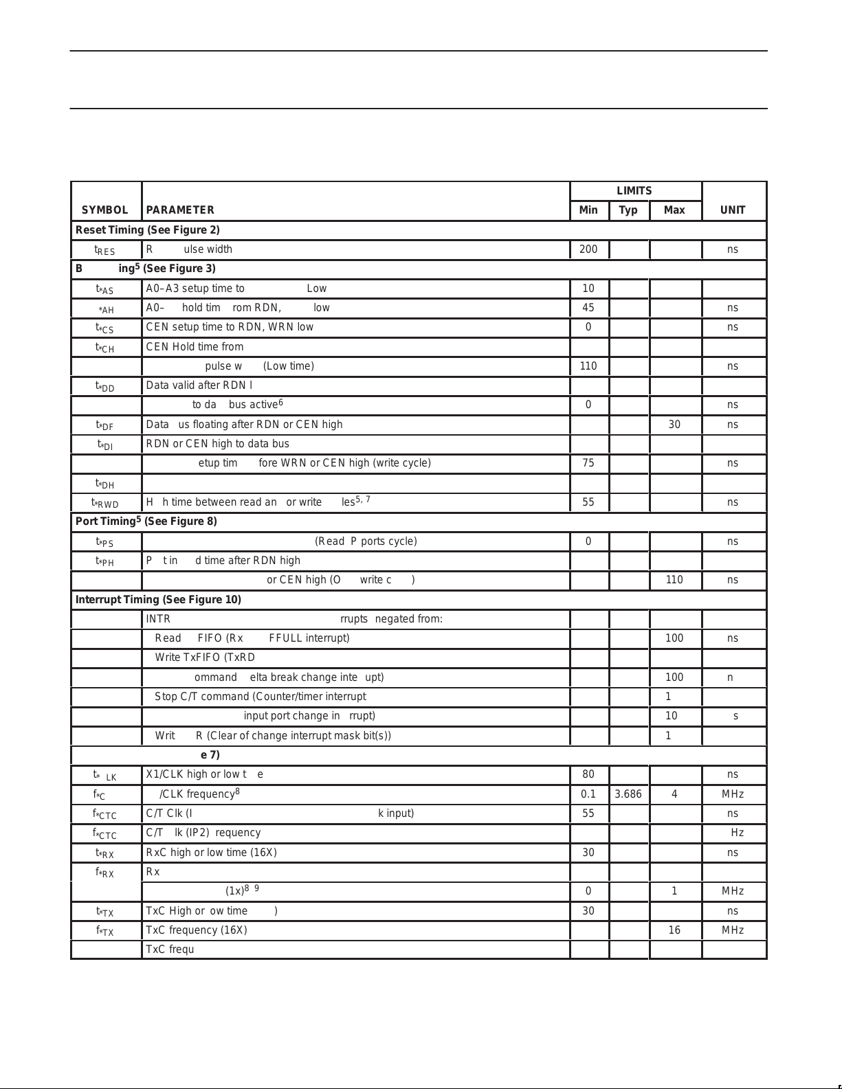
Philips Semiconductors Preliminary specification
Dual Universal Asynchronous
Receiver/Transmitter (DUART)
LIMITS
SYMBOL
SYMBOL
Transmitter Timing, external clock (See Figure 11)
t
*TXD
t
*TCS
Receiver Timing, external clock (See Figure 12)
t
*RXS
t
*RXH
NOTES:
1. Parameters are valid over specified temperature range.
2. All voltage measurements are referenced to ground (GND). For testing, all inputs swing between 0.4 V and 3.0 V with a transition time of
5 ns maximum. For X1/CLK this swing is between 0.4 V and 4.4 V . All time measurements are referenced at input voltages of 0.8 V and
2.0 V and output voltages of 0.8 V and 2.0 V , as appropriate.
3. Test conditions for outputs: CL = 150 pF, except interrupt outputs. Test conditions for interrupt outputs: CL = 50 pF , RL = 2.7 Kohm to V
Number 3 use 4.
4. Typical values are at +25C, typical supply voltages, and typical processing parameters.
5. Timing is illustrated and referenced to the WRN and RDN Inputs. Also, CEN may be the “strobing” input. CEN and RDN (also CEN and
WRN) are ORed internally. The signal asserted last initiates the cycle and the signal negated first terminates the cycle.
6. Guaranteed by characterization of sample units.
7. If CEN is used as the “strobing” input, the parameter defines the minimum High times between one CEN and the next. The RDN signal must
be negated for tRWD to guarantee that any status register changes are valid.
8. Minimum frequencies are not tested but are guaranteed by design.
9. Clocks for 1X mode should be symmetrical.
PARAMETER
PARAMETER
TxD output delay from TxC low (TxC input pin)
Output delay from TxC output pin low to TxD data output
RxD data setup time to RxC high
RxD data hold time from RxC high
Min
–30
100
100
Typ
SC28L92
UNIT
Max
120
30
UNIT
ns
ns
ns
ns
CC
.
1998 Oct 05
11
Page 12

Philips Semiconductors Preliminary specification
SYMBOL
FIGURE
PARAMETER
UNIT
10
Dual Universal Asynchronous
3
SC28L92
Max
16
16
1
1
MHz
MHz
MHz
MHz
Receiver/Transmitter (DUART)
(1X)
(1X)
1, 2, 3
LIMITS
Min Typ
0.1
100
0
0
AC CHARACTERISTICS (68XXX MODE)
= 5V ± 10%, T
V
CC
Reset Timing
t
RES
Bus Timing5
t
AS
t
AH
t
RWS
t
RWH
8
t
CSW
9
t
CSD
t
DD
8
t
DA
8
t
DF
8
t
DI
t
DS
t
DH
t
DAL
t
DCR
t
DCW
t
DAH
I
DAT
7
t
CSC
Port Timing
t
PS
t
PH
t
PD
Interrupt Timing
t
IR
Clock Timing
t
CLK
11
f
CLK
t
CTC
9
f
CTC
t
RX
9
f
RX
t
TX
9
f
TX
Transmitter Timing
t
TXD
t
TCS
Receiver Timing
t
RXS
t
RXH
NOTES:
1. Parameters are valid over specified temperature range.
2. All voltage measurements are referenced to ground (GND). For testing, all inputs swing between 0.4V and 2.4V with a transition time of 5ns
maximum. For X1/CLK this swing is between 0.4V and 4.4V . All time measurements are referenced at input voltages of 0.8V and 2.0V and
output voltages of 0.8V and 2.0V , as appropriate.
= –40C to 85C, unless otherwise specified.
A
4 RESET pulse width 200 ns
5,6,7 A1–A4 setup time to CSN Low 10 ns
5,6,7 A1–A4 hold time from CSN Low 45 ns
5,6,7 RWN setup time to CSN High 0 ns
5,6,7 RWN holdup time to CSN High 0 ns
5,6,7 CSN High pulse width 110 ns
5,6,7 CSN or IACKN High from DTACKN Low 20 ns
5,6,7 Data valid from CSN or IACKN Low 175 ns
5 RDN Low to data bus active 15 ns
5,6,7 Data bus floating from CSN or IACKN High 125 ns
5 RDN High to data bus invalid 20 ns
5,6,7 Data setup time to CLK High 100 ns
5,6,7 Data hold time from CSN High 0 ns
5,6,7 DTACKN Low from read data valid 0 ns
5,6,7 DTACKN Low (read cycle) from CLK High 125 ns
5,6,7 DTACKN Low (write cycle) form CLK High 125 ns
5,6,7 DTACKN High from CSN or IACKN High 100 ns
5,6,7 DTACKN High impedance from CSN or IACKN High 125 ns
5,6,7 CSN or IACKN setup time to clock High 90 ns
5
8 Port input setup time to CSN Low 0 ns
8 Port input hold time from CSN High 0 ns
8 Port output valid from CSN High 400 ns
7
INTRN (or OP3–OP7 when used as interrupts) negated from:
Read RHR (RxRDY/FFULL interrupt) 100 ns
Write THR (TxRDY interrupt) 100 ns
Reset command (break interrupt) 100 ns
Stop C/T command (counter interrupt) 100 ns
Read IPCR (input port change interrupt) 100 ns
Write IMR (clear of interrupt mask bit) 100 ns
10 X1/CLK High or Low time 80 ns
10 X1/CLK frequency 0 3.6864 4 MHz
10 CTCLK (IP2) High or Low time 55 ns
10 CTCLK (IP2) frequency 100 4 MHz
10 RxC High or Low time 50 ns
10
RxC frequency (16X)
10 TxC High or Low time 50 ns
10
TxC frequency (16X)
11 TxD output delay from TxC external clock input on IP pin 350 ns
11 Output delay from TxC low at OP pin to TxD data output 150 ns
12 RxD data setup time before RxC high at external clock input on IP pin 240 ns
12 RxD data hold time after RxC high at external clock input on IP pin 200 ns
1998 Oct 05
12
Page 13

Philips Semiconductors Preliminary specification
Dual Universal Asynchronous
Receiver/Transmitter (DUART)
3. Typical values are at +25°C, typical supply voltages, and typical processing parameters.
4. Test conditions for outputs: C
5. This specification will impose maximum 68000 CPU CLK to 6MHz. Higher CPU CLK can be used if repeating bus reads are not performed.
Consecutive write operations to the same command register require at least three edges of the X1 clock between writes.
6. This specification imposes a lower bound on CSN and IACKN Low, guaranteeing that it will be Low for at least 1 CLK period. This
requirement is made on CSN only to insure assertion of DTACKN and not to guarantee operation of the part.
7. This specification is made only to insure that DTACKN is asserted with respect to the rising edge of the X1/CLK pin as shown in the timing
diagram, not to guarantee operation of the part. If the setup time is violated, DTACKN may be asserted as shown, or may be asserted one
clock cycle later.
8. Guaranteed by characterization of sample units.
9. Minimum frequencies are not tested but are guaranteed by design.
10.325ns maximum for T
11.Operation to 0MHz is assured by design. Minimum test frequency is 2.0MHz.
12.See UART application note for power down currents less than 5µA.
= 150pF, except interrupt outputs. Test condition for interrupt outputs: CL = 50pF, R
L
> 70°C.
A
SC28L92
= 2.7kΩ to VCC.
L
1998 Oct 05
13
Page 14

Philips Semiconductors Preliminary specification
Dual Universal Asynchronous
Receiver/Transmitter (DUART)
Block Diagram
The SC28L92 DUART consists of the following eight major sections:
data bus buffer, operation control, interrupt control, timing,
communications Channels A and B, input port and output port. Refer
to the Block Diagram.
Data Bus Buffer
The data bus buffer provides the interface between the external and
internal data buses. It is controlled by the operation control block to
allow read and write operations to take place between the controlling
CPU and the DUART.
Operation Control
The operation control logic receives operation commands from the
CPU and generates appropriate signals to internal sections to
control device operation. It contains address decoding and read and
write circuits to permit communications with the microprocessor via
the data bus buffer.
Interrupt Control
A single active-Low interrupt output (INTRN) is provided which is
activated upon the occurrence of any of eight internal events.
Associated with the interrupt system are the Interrupt Mask Register
(IMR) and the Interrupt Status Register (ISR). The IMR can be
programmed to select only certain conditions to cause INTRN to be
asserted. The ISR can be read by the CPU to determine all currently
active interrupting conditions. Outputs OP3–OP7 can be
programmed to provide discrete interrupt outputs for the transmitter,
receivers, and counter/timer. When OP3 to OP7 are programmed as
interrupts, their output buffers are changed to the open drain active
low configuration.
FIFO Configuration
Each receiver and transmitter has a 16 byte FIFO. These FIFOs
may be configured to operate at a fill capacity of either 8 or 16 bytes.
This feature may be used if it is desired to operate the 28L92 in strict
compliance with the 26C92. The 8 byte/16 byte mode is controlled
by the MR0[3] bit. A 0 value for this bit sets the 8 bit mode ( the
default); a 1 sets the 16 byte mode.
The FIFO fill interrupt level automatically follow the programming of
the MR0[3] bit. See tables 3 and 4.
TIMING CIRCUITS
Crystal Clock
The timing block consists of a crystal oscillator, a baud rate
generator, a programmable 16-bit counter/timer, and four clock
selectors. The crystal oscillator operates directly from a crystal
connected across the X1/CLK and X2 inputs. If an external clock of
the appropriate frequency is available, it may be connected to
X1/CLK. The clock serves as the basic timing reference for the Baud
Rate Generator (BRG), the counter/timer, and other internal circuits.
A clock signal within the limits specified in the specifications section
of this data sheet must always be supplied to the DUART. If an
external is used instead of a crystal, X1 should be driven using a
configuration similar to the one in Figure 7.
BRG
The baud rate generator operates from the oscillator or external
clock input and is capable of generating 18 commonly used data
communications baud rates ranging from 50 to 38.4K baud.
SC28L92
Programming bit 0 of MR0 to a “1” gives additional baud rates of
57.6kB, 115.2kB and 230.4kB. These will be in the 16X mode. A
3.6864 MHz crystal or external clock must be used to get the
standard baud rate. The clock outputs from the BRG are at 16X the
actual baud rate. The counter/timer can be used as a timer to
produce a 16X clock for any other baud rate by counting down the
crystal clock or an external clock. The four clock selectors allow the
independent selection, for each receiver and transmitter, of any of
these baud rates or external timing signal.
Counter/Timer (C/T)
The counter timer is a 16-bit programmable divider that operates in
one of three modes: counter, timer, time out. In the timer mode it
generates a square wave. In the counter mode it generates a time
delay. In the time out mode it monitors the time between received
characters. The C/T uses the numbers loaded into the
Counter/Timer Lower Register (CTLR) and the Counter/T imer Upper
Register (CTUR) as its divisor. The counter timer is controlled with
six commands: Start/Stop C/T, Read/Write Counter/Timer lower
register and Read/Write Counter/Timer upper register. These
commands have slight differences depending on the mode of
operation. Please see the detail of the commands under the
CTLR/CTUR Register descriptions.
Communications Channels A and B
Each communications channel of the SC28L92 comprises a
full-duplex asynchronous receiver/transmitter (UART). The operating
frequency for each receiver and transmitter can be selected
independently from the baud rate generator, the counter/timer, or
from an external input. The transmitter accepts parallel data from the
CPU, converts it to a serial bit stream, inserts the appropriate start,
stop, and optional parity bits and outputs a composite serial stream
of data on the TxD output pin. The receiver accepts serial data on
the RxD pin, converts this serial input to parallel format, checks for
start bit, stop bit, parity bit (if any), or break condition and sends an
assembled character to the CPU via the receive FIFO. Three status
bits (Break, Framing and Parity Errors) are also FIFOed with each
data character.
Input Port
The inputs to this unlatched 7-bit (6-bit for 68xxx mode) port can be
read by the CPU by performing a read operation at address H’D’. A
High input results in a logic 1 while a Low input results in a logic 0.
D7 will always read as a logic 1. The pins of this port can also serve
as auxiliary inputs to certain portions of the DUART logic.
Four change-of-state detectors are provided which are associated
with inputs IP3, IP2, IP1 and IP0. A High-to-Low or Low-to-High
transition of these inputs, lasting longer than 25–50 ms, will set the
corresponding bit in the input port change register. The bits are
cleared when the register is read by the CPU. Any change-of-state
can also be programmed to generate an interrupt to the CPU.
The input port pulse detection circuitry uses a 38.4 KHz sampling
clock derived from one of the baud rate generator taps. This results in
a sampling period of slightly more than 25 ms (this assumes that the
clock input is 3.6864 MHz). The detection circuitry, in order to
guarantee that a true change in level has occurred, requires two
successive samples at the new logic level be observed. As a
consequence, the minimum duration of the signal change is 25 ms if
the transition occurs “coincident with the first sample pulse”. The
50 s time refers to the situation in which the change-of-state is “just
missed” and the first change-of-state is not detected until 25 ms later.
1998 Oct 05
14
Page 15

Philips Semiconductors Preliminary specification
Dual Universal Asynchronous
Receiver/Transmitter (DUART)
Output Port
The output port pins may be controlled by the OPR, OPCR, MR and
CR registers. Via appropriate programming they may be just another
parallel port to external circuits, or they may represent many internal
conditions of the UART. When this 8-bit port is used as a general
purpose output port, the output port pins drive a state which is the
(pg. 9 start) complement of the Output Port Register (OPR). The
OPR register is set and reset by writing to the SOPR and ROPR
addresses. (See the description of the SOPR and ROPR registers).
The output pins will drive the inverse data polarity of the OPR
registers. The OPCR register conditions these output pins to be
controlled by the OPR or by other signals in the chip. Output ports
are driven high on hardware reset.
OPERATION
Transmitter
The SC28L92 is conditioned to transmit data when the transmitter is
enabled through the command register. The SC28L92 indicates to
the CPU that it is ready to accept a character by setting the TxRDY
bit in the status register. This condition can be programmed to
generate an interrupt request at OP6 or OP7 and INTRN. When the
transmitter is initially enabled the TxRDY and TxEMPT bits will be
set in the status register. When a character is loaded to the transmit
FIFO the TxEMPT bit will be reset. The TxEMPT will not set until: 1)
the transmit FIFO is empty and the transmit shift register has
finished transmitting the stop bit of the last character written to the
transmit FIFO, or 2) the transmitter is disabled and then re-enabled.
The TxRDY bit is set whenever the transmitter is enabled and the
TxFIFO is not full. Data is transferred from the holding register to
transmit shift register when it is idle or has completed transmission
of the previous character. Characters cannot be loaded into the
TxFIFO while the transmitter is disabled.
The transmitter converts the parallel data from the CPU to a serial
bit stream on the TxD output pin. It automatically sends a start bit
followed by the programmed number of data bits, an optional parity
bit, and the programmed number of stop bits. The least significant
bit is sent first. Following the transmission of the stop bits, if a new
character is not available in the TxFIFO, the TxD output remains
High and the TxEMT bit in the Status Register (SR) will be set to 1.
Transmission resumes and the TxEMT bit is cleared when the CPU
loads a new character into the TxFIFO.
If the transmitter is disabled, it continues operating until the
character currently being transmitted is completely sent out. The
transmitter can be forced to send a continuous Low condition by
issuing a send break command. The transmitter can be reset
through a software command. If it is reset, operation ceases
immediately and the transmitter must be enabled through the
command register before resuming operation. If CTS option is
enabled (MR2[4] = 1), the CTS input at IP0 or IP1 must be Low in
order for the character to be transmitted. The transmitter will check
the state of the CTS input at the beginning of each character
transmitted. If it is found to be High, the transmitter will delay the
transmission of any following characters until the CTS has returned
to the low state. CTS going high during the serialization of a
character will not affect that character.
The transmitter can also control the RTSN outputs, OP0 or OP1 via
MR2[5]. When this mode of operation is set, the meaning of the OP0
or OP1 signals will usually be ‘end of message’. See description of
the MR2[5] bit for more detail.
SC28L92
Receiver
The SC28L92 is conditioned to receive data when enabled through
the command register. The receiver looks for a High-to-Low
(mark-to-space) transition of the start bit on the RxD input pin. If a
transition is detected, the state of the RxD pin is sampled each 16X
clock for 7-1/2 clocks (16X clock mode) or at the next rising edge of
the bit time clock (1X clock mode). If RxD is sampled High, the start
bit is invalid and the search for a valid start bit begins again. If RxD
is still Low, a valid start bit is assumed and the receiver continues to
sample the input at one bit time intervals at the theoretical center of
the bit, until the proper number of data bits and parity bit (if any)
have been assembled, and one stop bit has been detected. The
least significant bit is received first. The data is then transferred to
the Receive FIFO and the RxRDY bit in the SR is set to a 1. This
condition can be programmed to generate an interrupt at OP4 or
OP5 and INTRN. If the character length is less than 8 bits, the most
significant unused bits in the RxFIFO are set to zero.
After the stop bit is detected, the receiver will immediately look for
the next start bit. However, if a non-zero character was received
without a stop bit (framing error) and RxD remains Low for one half
of the bit period after the stop bit was sampled, then the receiver
operates as if a new start bit transition had been detected at that
point (one-half bit time after the stop bit was sampled).
The parity error, framing error, and overrun error (if any) are strobed
into the SR at the received character boundary, before the RxRDY
status bit is set. If a break condition is detected (RxD is Low for the
entire character including the stop bit), a character consisting of all
zeros will be loaded into the RxFIFO and the received break bit in
the SR is set to 1. The RxD input must return to high for two (2)
clock edges of the X1 crystal clock for the receiver to recognize the
end of the break condition and begin the search for a start bit.
This will usually require a high time of one X1 clock period or 3
X1 edges since the clock of the controller is not synchronous
to the X1 clock.
Receiver FIFO
The RxFIFO consists of a First-In-First-Out (FIFO) stack with a
capacity of 8 or 16 characters. Data is loaded from the receive shift
register into the topmost empty position of the FIFO. The RxRDY bit
in the status register is set whenever one or more characters are
available to be read, and a FFULL status bit is set if all 8 or 16 stack
positions are filled with data. Either of these bits can be selected to
cause an interrupt. A read of the RxFIFO outputs the data at the top
of the FIFO. After the read cycle, the data FIFO and its associated
status bits (see below) are ‘popped’ thus emptying a FIFO position
for new data.
Receiver Status Bits
In addition to the data word, three status bits (parity error, framing
error, and received break) are also appended to each data character
in the FIFO (overrun is not). Status can be provided in two ways, as
programmed by the error mode control bit in the mode register. In
the ‘character’ mode, status is provided on a character-by-character
basis; the status applies only to the character at the top of the FIFO.
In the ‘block’ mode, the status provided in the SR for these three bits
is the logical-OR of the status for all characters coming to the top of
the FIFO since the last ‘reset error’ command was issued. In either
mode reading the SR does not affect the FIFO. The FIFO is
‘popped’ only when the RxFIFO is read. Therefore the status
register should be read prior to reading the FIFO.
1998 Oct 05
15
Page 16

Philips Semiconductors Preliminary specification
Dual Universal Asynchronous
Receiver/Transmitter (DUART)
If the FIFO is full when a new character is received, that character is
held in the receive shift register until a FIFO position is available. If
an additional character is received while this state exits, the
contents of the FIFO are not affected; the character previously in the
shift register is lost and the overrun error status bit (SR[4] will be
set-upon receipt of the start bit of the new (overrunning) character).
The receiver can control the deactivation of RTS. If programmed to
operate in this mode, the RTSN output will be negated when a valid
start bit was received and the FIFO is full. When a FIFO position
becomes available, the RTSN output will be re-asserted
automatically. This feature can be used to prevent an overrun, in the
receiver, by connecting the RTSN output to the CTSN input of the
transmitting device.
If the receiver is disabled, the FIFO characters can be read.
However, no additional characters can be received until the receiver
is enabled again. If the receiver is reset, the FIFO and all of the
receiver status, and the corresponding output ports and interrupt are
reset. No additional characters can be received until the receiver is
enabled again.
Receiver Reset and Disable
Receiver disable stops the receiver immediately—data being
assembled in the receiver shift register is lost. Data and status in the
FIFO is preserved and may be read. A re-enable of the receiver
after a disable will cause the receiver to begin assembling
characters at the next start bit detected. A receiver reset will discard
the present shift register date, reset the receiver ready bit (RxRDY),
clear the status of the byte at the top of the FIFO and re-align the
FIFO read/write pointers.
A ‘watchdog timer’ is associated with each receiver. Its interrupt is
enabled by MR0[7]. The purpose of this timer is to alert the control
processor that characters are in the RxFIFO which have not been
read and/or the data stream has stopped. This situation may occur
at the end of a transmission when the last few characters received
are not sufficient to cause an interrupt.
This counter times out after 64 bit times. It is reset each time a
character is transferred from the receiver shift register to the
RxFIFO or a read of the RxFIFO is executed.
Receiver Time-out Mode
In addition to the watch dog timer described in the receiver section,
the counter/timer may be used for a similar function. Its
programmability, of course, allows much greater precision of time
out intervals.
The time-out mode uses the received data stream to control the
counter. Each time a received character is transferred from the shift
register to the RxFIFO, the counter is restarted. If a new character is
not received before the counter reaches zero count, the counter
ready bit is set, and an interrupt can be generated. This mode can
be used to indicate when data has been left in the RxFIFO for more
than the programmed time limit. Otherwise, if the receiver has been
programmed to interrupt the CPU when the receive FIFO is full, and
the message ends before the FIFO is full, the CPU may not know
there is data left in the FIFO. The CTU and CTL value would be
programmed for just over one character time, so that the CPU would
be interrupted as soon as it has stopped receiving continuous data.
This mode can also be used to indicate when the serial line has
been marking for longer than the programmed time limit. In this
case, the CPU has read all of the characters from the FIFO, but the
last character received has started the count. If there is no new data
SC28L92
during the programmed time interval, the counter ready bit will get
set, and an interrupt can be generated.
The time-out mode is enabled by writing the appropriate command
to the command register . Writing an ‘Ax’ to CRA or CRB will invoke
the time-out mode for that channel. Writing a ‘Cx’ to CRA or CRB
will disable the time-out mode. The time-out mode should only be
used by one channel at once, since it uses the C/T. If, however, the
time-out mode is enabled from both receivers, the time-out will occur
only when both receivers have stopped receiving data for the
time-out period. CTU and CTL must be loaded with a value greater
than the normal receive character period. The time-out mode
disables the regular STAR T/STOP Counter commands and puts the
ca/T into counter mode under the control of the received data
stream. Each time a received character is transferred from the shift
register to the RxFIFO, the C/T is stopped after 1 C/T clock,
reloaded with the value in CTU and CTL and then restarted on the
next C/T clock. If the C/T is allowed to end the count before a new
character has been received, the counter ready bit, ISR[3], will be
set. If IMR[3] is set, this will generate an interrupt. Receiving a
character after the C/T has timed out will clear the counter ready bit,
ISR[3], and the interrupt. Invoking the ‘Set Time-out Mode On’
command, CRx = ‘Ax’, will also clear the counter ready bit and stop
the counter until the next character is received.
Time Out Mode Caution
When operating in the special time out mode, it is possible to
generate what appears to be a “false interrupt”, i.e., an interrupt
without a cause. This may result when a time-out interrupt occurs
and then, BEFORE the interrupt is serviced, another character is
received, i.e., the data stream has started again. (The interrupt
latency is longer than the pause in the data stream.) In this case,
when a new character has been receiver, the counter/timer will be
restarted by the receiver, thereby withdrawing its interrupt. If, at this
time, the interrupt service begins for the previously seen interrupt, a
read of the ISR will show the “Counter Ready” bit not set. If nothing
else is interrupting, this read of the ISR will return a x’00 character.
Multi-drop Mode (9-bit or Wake-Up)
The DUART is equipped with a wake up mode for multi-drop
applications. This mode is selected by programming bits
MR1A[4:3]or MR1B[4:3] to ‘11’ for Channels A and B, respectively.
In this mode of operation, a ‘master’ station transmits an address
character followed by data characters for the addressed ‘slave’
station. The slave stations, with receivers that are normally disabled,
examine the received data stream and ‘wakeup’ the CPU (by setting
RxRDY)only upon receipt of an address character. The CPU
compares the received address to its station address and enables
the receiver if it wishes to receive the subsequent data characters.
Upon receipt of another address character, the CPU may disable the
receiver to initiate the process again.
A transmitted character consists of a start bit, the programmed
number of data bits, and Address/Data (A/D) bit, and the
programmed number of stop bits. The polarity of the transmitted A/D
bit is selected by the CPU by programming bit MR1A[2]/MR1B[2].
MR1A[2]/MR1B[2] = 0 transmits a zero in the A/D bit position, which
identifies the corresponding data bits as data while
MR1A[2]/MR1B[2] = 1 transmits a one in the A/D bit position, which
identifies the corresponding data bits as an address. The CPU
should program the mode register prior to loading the corresponding
data bits into the TxFIFO.
1998 Oct 05
16
Page 17
Philips Semiconductors Preliminary specification
Á
Dual Universal Asynchronous
Receiver/Transmitter (DUART)
In this mode, the receiver continuously looks at the received data
stream, whether it is enabled or disabled. If disabled, it sets the
RxRDY status bit and loads the character into the RxFIFO if the
received A/D bit is a one (address tag), but discards the received
character if the received A/D bit is a zero (data tag). If enabled, all
received characters are transferred to the CPU via the RxFIFO. In
either case, the data bits are loaded into the data FIFO while the
A/D bit is loaded into the status FIFO position normally used for
parity error (SRA[5] or SRB[5]). Framing error, overrun error, and
break detect operate normally whether or not the receive is enabled.
PROGRAMMING
The operation of the DUART is programmed by writing control words
into the appropriate registers. Operational feedback is provided via
status registers which can be read by the CPU. The addressing of
the registers is described in Table 1.
The contents of certain control registers are initialized to zero on
RESET. Care should be exercised if the contents of a register are
changed during operation, since certain changes may cause
operational problems.
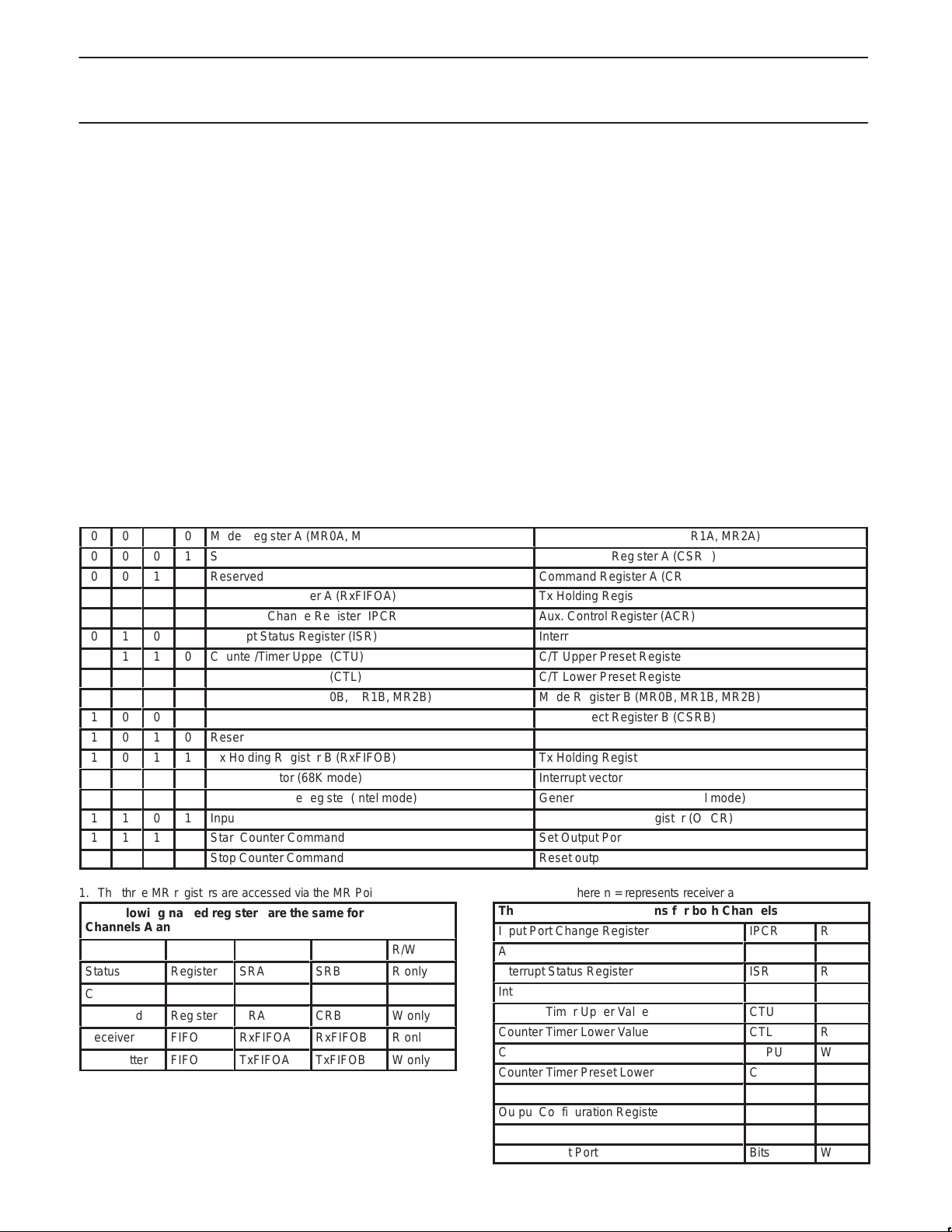
Table 1. SC28L92 register addressing READ (RDN = 0), WRITE (WRN = 0)
0
0
0
0
Mode Register A (MR0A, MR1A, MR2A)
0
0
0
1
Status Register A (SRA)
0
0
1
0
Reserved
0
0
1
1
Rx Holding Register A (RxFIFOA)
0
1
0
0
Input Port Change Register (IPCR)
0
1
0
1
Interrupt Status Register (ISR)
0
1
1
0
Counter/Timer Upper (CTU)
0
1
1
1
Counter/Timer Lower (CTL)
1
0
0
0
Mode Register B (MR0B, MR1B, MR2B)
1
0
0
1
Status Register B (SRB)
1
0
1
0
Reserved
1
0
1
1
Rx Holding Register B (RxFIFOB)
1
1
0
0
Interrupt vector (68K mode)
1
1
0
0
General purpose register (Intel mode)
1
1
0
1
Input Port (IPR)
1
1
1
0
Start Counter Command
1
1
1
1
Stop Counter Command
NOTE:
1. The three MR registers are accessed via the MR Pointer and Commands 0x1n and 0xBn (where n = represents receiver and transmitter enable bits)
The following named registers are the same for
БББББББББББББББ
Channels A and B
Mode
Status
Clock
Command
Receiver
Transmitter
Register
Register
Select
Register
FIFO
FIFO
MRnA
SRA
CSRA
CRA
RxFIFOA
TxFIFOA
MRnB
SRB
CSRB
CRB
RxFIFOB
TxFIFOB
R/W
R only
W only
W only
R only
W only
For example, changing the number of bits per character while the
transmitter is active may cause the transmission of an incorrect
character. In general, the contents of the MR, the CSR, and the
OPCR should only be changed while the receiver(s) and
transmitter(s) are not enabled, and certain changes to the ACR
should only be made while the C/T is stopped.
Each channel has 3 mode registers (MR0, 1, 2) which control the
basic configuration of the channel. Access to these registers is
controlled by independent MR address pointers. These pointers are
set to 0 or 1 by MR control commands in the command register
“Miscellaneous Commands”. Each time the MR registers are
accessed the MR pointer increments, stopping at MR2. It remains
pointing to MR2 until set to 0 or 1 via the miscellaneous commands
of the command register. The pointer is set to 1 on reset for
compatibility with previous Philips Semiconductors UART software.
Mode, command, clock select, and status registers are duplicated
for each channel to provide total independent operation and control.
Refer to Table 2 for register bit descriptions. The reserved registers
at addresses H‘02’ and H‘0A’ should never be read during normal
operation since they are reserved for internal diagnostics.
Mode Register A (MR0A, MR1A, MR2A)
Clock Select Register A (CSRA)
Command Register A (CRA)
Tx Holding Register A (TxFIFOA)
Aux. Control Register (ACR)
Interrupt Mask Register (IMR)
C/T Upper Preset Register (CTPU)
C/T Lower Preset Register (CTPL)
Mode Register B (MR0B, MR1B, MR2B)
Clock Select Register B (CSRB)
Command Register B (CRB)
Tx Holding Register B (TxFIFOB)
Interrupt vector (68K mode)
General purpose register (Intel mode)
Output Port Conf. Register (OPCR)
Set Output Port Bits Command (SOPR)
Reset output Port Bits Command (ROPR)
These are support functions for both Channels
Input Port Change Register
Auxiliary Control Register
Interrupt Status Register
Interrupt Mask Register
Counter Timer Upper Value
Counter Timer Lower Value
Counter Timer Preset Upper
Counter Timer Preset Lower
Input Port Register
Output Configuration Register
Set Output Port
Reset Output Port
SC28L92
IPCR
ACR
ISR
IMR
CTU
CTL
CTPU
CTPL
IPR
OPCR
Bits
Bits
R
W
R
W
R
R
W
W
R
W
W
W
1998 Oct 05
17
Page 18
Philips Semiconductors Preliminary specification
Á
Á
Á
Á
Á
Á
Á
Á
БББББ
БББББ
Dual Universal Asynchronous
Receiver/Transmitter (DUART)
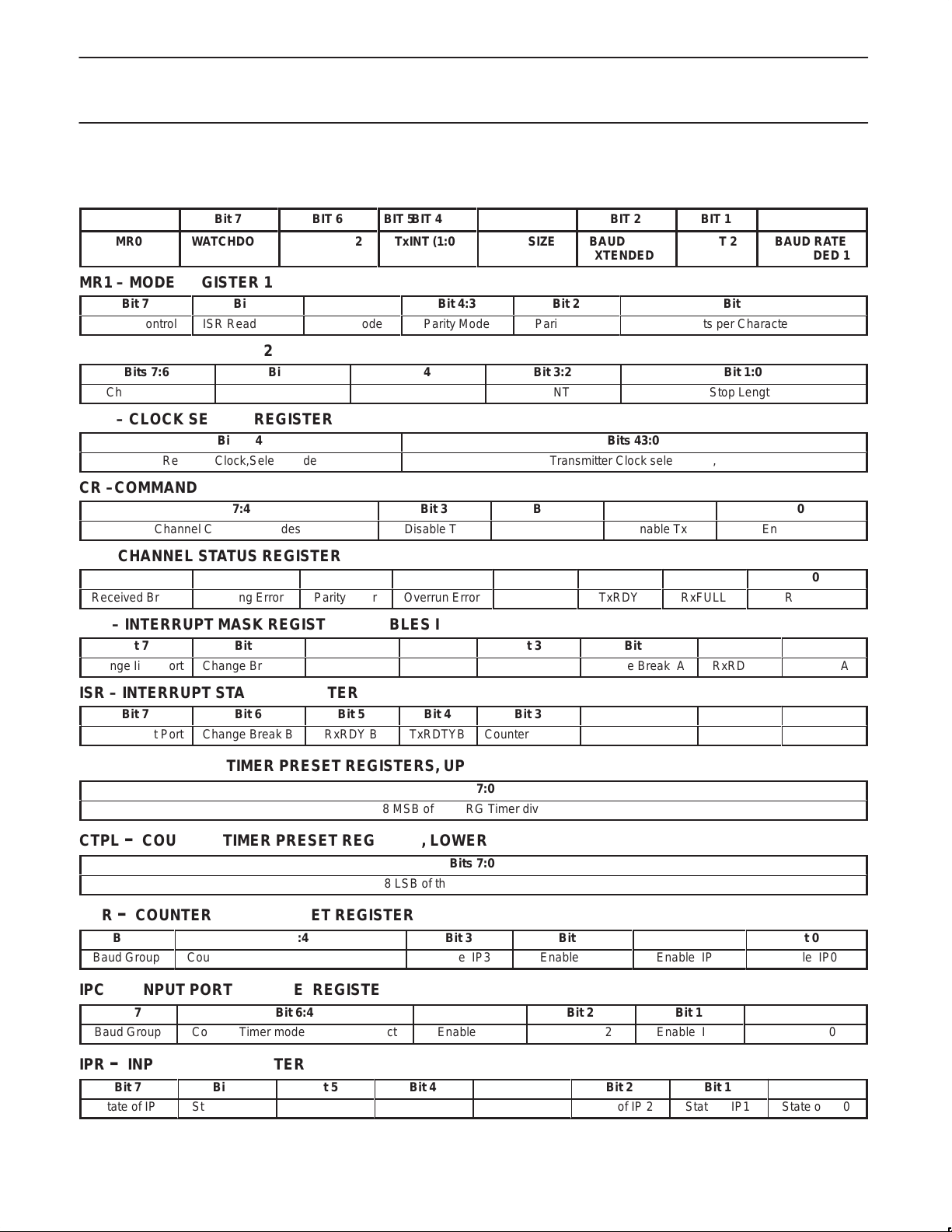
Table 2. Register bit formats
MR0 – MODE REGISTER 0
Bit 7
MR0
ÁÁÁ
WATCHDOG
ÁÁÁ
MR1 – MODE REGISTER 1
Bit 7
RxRTS Control
Bit 6
ISR Read Mode
MR2 – MODE REGISTER 2
Bits 7:6
Channel Mode
TxRTS Control
CSR – CLOCK SELECT REGISTER
Bits 7:4
Receiver Clock,Select Code
CR –COMMAND REGISTER
Bits 7:4
Channel Command codes
BIT 6
RxINT BIT 2
ÁÁÁ
Bit 5
Error Mode
Bit 5
BIT 5BIT 4
TxINT (1:0)
ÁÁÁ
Bit 4:3
Parity Mode
Bit 4
CTSN Enable Tx
Bit 3
Disable Tx
BIT 3
FIFO SIZE
ÁÁÁÁ
Bit 2
Parity Type
Bit 3:2
RxINT
Transmitter Clock select code,
Bit 2
Enable Tx
BIT 2
BAUD RATE
EXTENDED II
ÁÁÁ
Bits 43:0
Bit 1
Enable Tx
SC28L92
BIT 1
TEST 2
ÁÁ
Bit 1:0
Bits per Character
Bit 1:0
Stop Length
BAUD RATE
EXTENDED 1
ÁÁÁÁ
Bit 0
Enable Rx
BIT 0
SR – CHANNEL STATUS REGISTER
Bit 7
Received Break
Bit 6
Framing Error
Bit 5
Parity Error
Bit 4
Overrun Error
Bit 3
TxEMT
IMR – INTERRUPT MASK REGISTER (ENABLES INTERRUPTS)
Bit 7
Change Iiput Port
Bit 6
Change Break B
Bit 5
RxRDY B
Bit 4
TxRDTYB
Bit 3
Counter Ready
ISR – INTERRUPT STATUS REGISTER
Bit 7
Change Iiput Port
Bit 6
Change Break B
Bit 5
RxRDY B
Bit 4
TxRDTYB
Bit 3
Counter Ready
CTPU – COUNTER TIMER PRESET REGISTERS, UPPER
Bits 7:0
8 MSB of the BRG Timer divisor.
CTPL – COUNTER TIMER PRESET REGISTER, LOWER
Bits 7:0
8 LSB of the BRG Timer divisor.
ACR – COUNTER TIMER PRESET REGISTER
Bit 7
Baud Group
Counter Timer mode and clock select
Bit 6:4
Bit 3
Enable IP3
IPCR – INPUT PORT CHANGE REGISTER
Bit 7
Baud Group
Counter Timer mode and clock select
Bit 6:4
Bit 3
Enable IP3
Change Break A
Change Break A
Bit 2
Enable IP2
Bit 2
Enable IP2
Bit 2
TxRDY
Bit 2
Bit 2
Bit 1
RxFULL
Bit 1
Enable IP1
Bit 1
Enable IP1
Bit 1
RxRDY A
Bit 1
RxRDY A
Bit 0
RxRDY
Bit 0
TxRDY A
Bit 0
TxRDY A
Bit 0
Enable IP0
Bit 0
Enable IP0
IPR – INPUT PORT REGISTER
State of IP
1998 Oct 05
Bit 7
Bit 6
State of IP 6
Bit 5
State of IP 5
Bit 4
State of IP 4
State of IP 3
18
Bit 3
Bit 2
State of IP 2
Bit 1
State of IP1
Bit 0
State of IP 0
Page 19
Philips Semiconductors Preliminary specification
Á
Á
Á
Á
Á
Á
Á
Á
Á
Á
Á
Á
Á
Á
Á
Á
Dual Universal Asynchronous
Receiver/Transmitter (DUART)
REGISTER DESCRIPTIONS Mode Registers
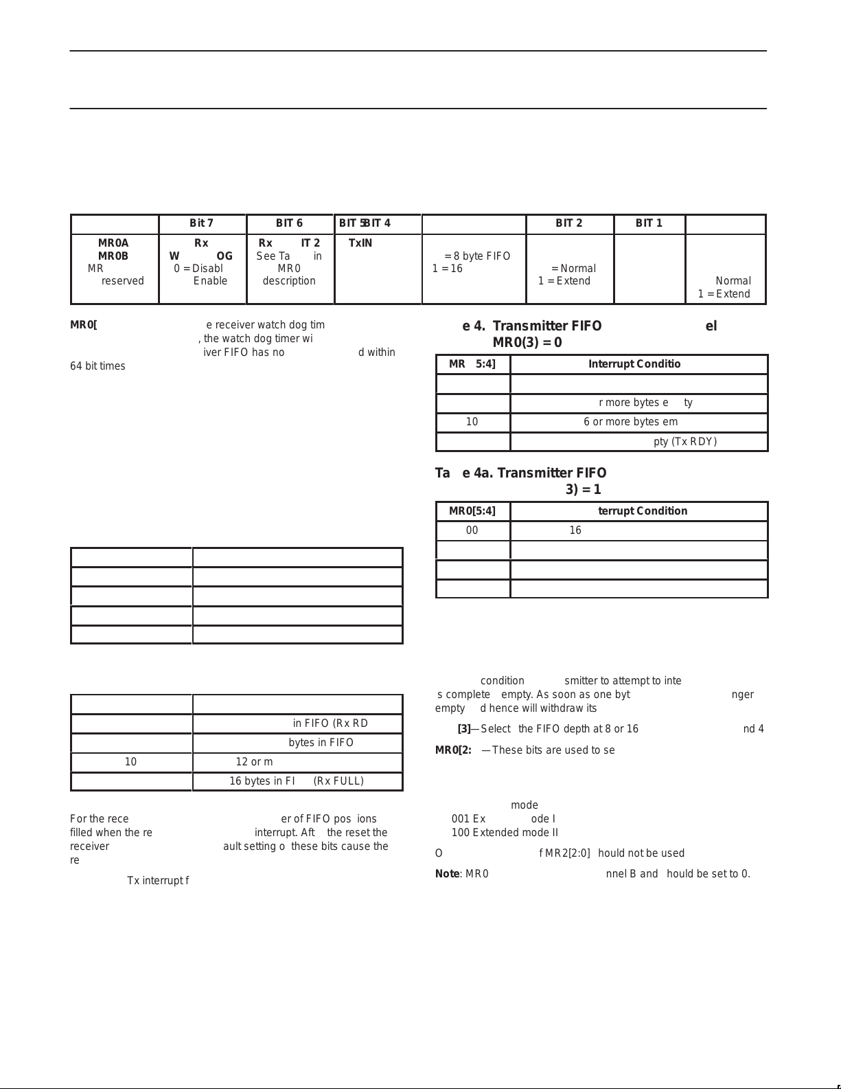
MR0a
MR0 Mode Register 0 MR0 is accessed by setting the MR pointer to 0 via the command register command B.
Bit 7
MR0A
MR0B
MR0B[3:0]
ÁÁÁ
are reserved
ÁÁÁ
Rx
WATCHDOG
0 = Disable
ÁÁÁ
1 = Enable
ÁÁÁ
MR0[7]—This bit controls the receiver watch dog timer. 0 = disable, 1 = enable. When enabled, the watch dog timer will generate a receiver interrupt if the receiver FIFO has not been accessed within 64 bit times of the receiver 1X clock. This is used to alert the control processor that data is in the RxFIFO that has not been read. This situation may occur when the byte count of the last part of a message is not large enough to generate an interrupt.
MR0[6]—Bit 2 of receiver FIFO interrupt level. This bit along with Bit 6 of MR1 sets the fill level of the FIFO that generates the receiver interrupt.
MR0[6] MR1[6] Note that this control is split between MR0 and
MR1. This is for backward compatibility to the SC2692 and
SCN2681.
Table 3. Receiver FIFO interrupt fill level
(MR0(3) = 0
MR0[6] MR1[6]
00
1 or more bytes in FIFO (Rx RDY)
01
10
11
8 bytes in FIFO (Rx FULL)
Table 3a. Receiver FIFO interrupt fill
level(MR0(3)=1
MR0[6] MR1[6]
00
01
10
11
For the receiver these bits control the number of FIFO positions
filled when the receiver will attempt to interrupt. After the reset the
receiver FIFO is empty. The default setting of these bits cause the
receiver to attempt to interrupt when it has one or more bytes in it.
MR0[5:4]—Tx interrupt fill level.
1 or more bytes in FIFO (Rx RDY)
16 bytes in FIFO (Rx FULL)
BIT 6
BIT 5BIT 4
RxINT BIT 2
See Tables in
MR0
ÁÁÁ
description
ÁÁÁ
See table #4
ÁÁÁ
ÁÁÁ
Interrupt Condition
3 or more bytes in FIFO
6 or more bytes in FIFO
Interrupt Condition
8 or more bytes in FIFO
12 or more bytes in FIFO
TxINT (1:0)
BIT 3
FIFO SIZE
0 = 8 byte FIFO
1 = 16 byte FIFO
ÁÁÁÁ
ÁÁÁÁ
BIT 2
BAUD RATE
EXTENDED II
0 = Normal
ÁÁÁÁ
1 = Extend II
ÁÁÁÁ
Table 4. Transmitter FIFO interrupt fill level
MR0(3) = 0
MR0[5:4]
00
01
10
11
Interrupt Condition
8 bytes empty (Tx EMPTY)
4 or more bytes empty
6 or more bytes empty
1 or more bytes empty (Tx RDY)
Table 4a. Transmitter FIFO interrupt fill
level MR0(3) = 1
MR0[5:4]
00
01
10
11
For the transmitter these bits control the number of FIFO positions
empty when the transmitter will attempt to interrupt. After the reset
the transmit FIFO has 8 bytes empty. It will then attempt to interrupt
as soon as the transmitter is enabled. The default setting of the MR0
bits (5:4) condition the transmitter to attempt to interrupt only when it
is completely empty . As soon as one byte is loaded, it is no longer
empty and hence will withdraw its interrupt request.
MR0[3]—Selects the FIFO depth at 8 or 16 bytes. See Tables 3 and 4 MR0[2:0]—These bits are used to select one of the six baud rate
groups.
See Table 5 for the group organization.
000 Normal mode
001 Extended mode I
100 Extended mode II
Other combinations of MR2[2:0] should not be used
Note: MR0[3:0] are not used in channel B and should be set to 0.
Interrupt Condition
16 bytes empty (Tx EMPTY)
8 or more bytes empty
12 or more bytes empty
1 or more bytes empty (Tx RDY)
BIT 1
TEST 2
Set to 0
ÁÁ
ÁÁ
SC28L92
BIT 0
BAUD RATE
EXTENDED
1
ÁÁÁ
0 = Normal
ÁÁÁ
1 = Extend
1998 Oct 05
19
Page 20
Philips Semiconductors Preliminary specification
Á
Á
Á
Á
Á
Á
Á
Á
Á
Á
Á
Á
Á
MR2B
Dual Universal Asynchronous
Receiver/Transmitter (DUART)
MR1A
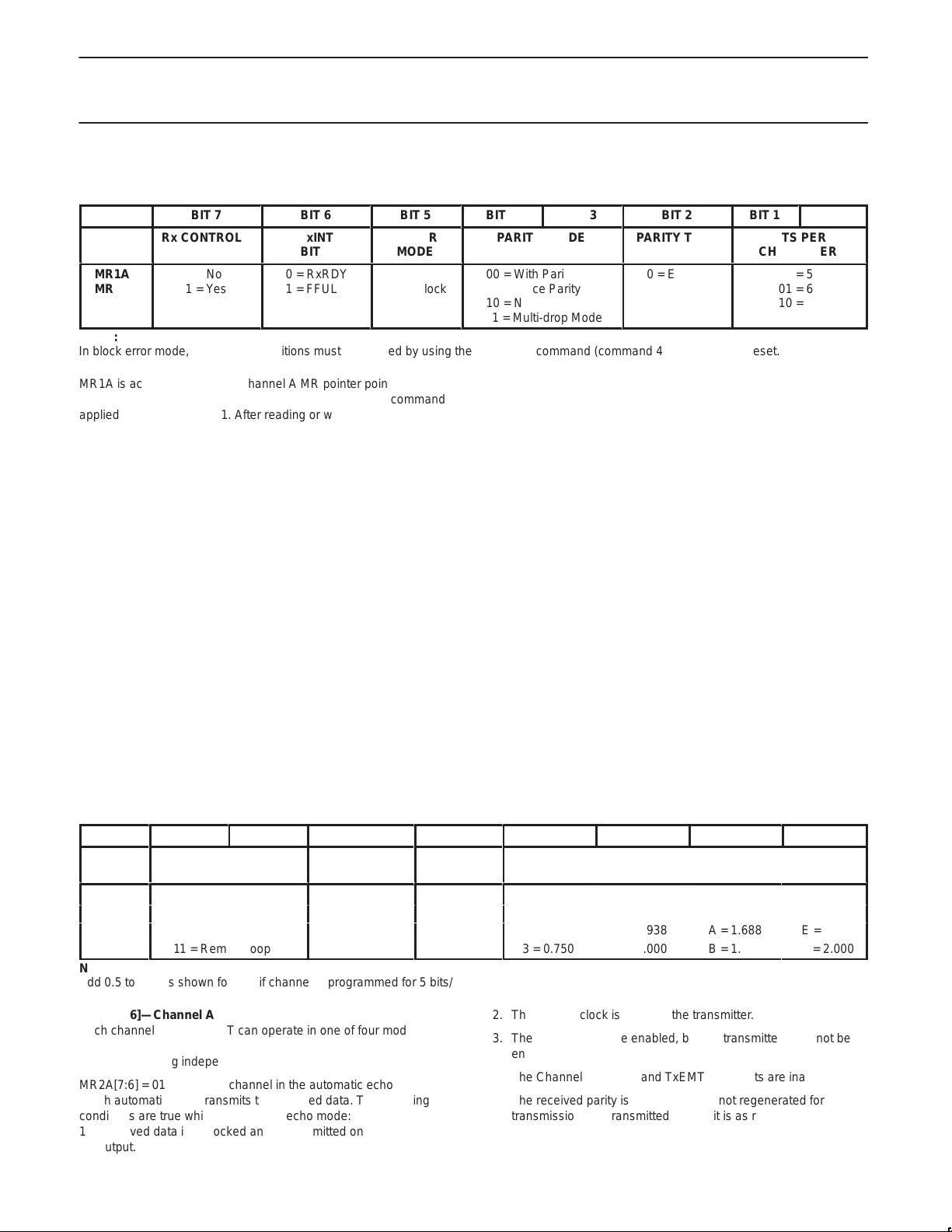
MR1 Mode Register 1
BIT 7
Rx CONTROLS
ÁÁÁÁÁÁ
MR1A
MR1B
ÁÁ
RTS
0 = No
1 = Yes
ÁÁÁ
NOTE:
In block error mode, block error conditions must be cleared by using the error reset command (command 4x) or a receiver reset.
MR1A is accessed when the Channel A MR pointer points to MR1.
The pointer is set to MR1 by RESET or by a ‘set pointer’ command
applied via CR command 1. After reading or writing MR1A, the
pointer will point to MR2A.
MR1A[7]—Channel A Receiver Request-to-Send Control
(Flow Control)
This bit controls the deactivation of the RTSAN output (OP0) by the
receiver. This output is normally asserted by setting OPR[0] and
negated by resetting OPR[0].
MR1A[7] = 1 causes RTSAN to be negated (OP0 is driven to a ‘1’
[V
]) upon receipt of a valid start bit if the Channel A FIFO is full.
CC
This is the beginning of the reception of the ninth byte. If the FIFO is
not read before the start of the tenth byte, an overrun condition will
occur and the tenth byte will be lost. However, the bit in OPR[0] is
not reset and RTSAN will be asserted again when an empty FIFO
position is available. This feature can be used for flow control to
prevent overrun in the receiver by using the RTSAN output signal to
control the CTSN input of the transmitting device.
MR1[6]—Bit 1 of the receiver interrupt control. See description under MR0[6].
MR1A[5]—Channel A Error Mode Select
This bit select the operating mode of the three FIFOed status bits
(FE, PE, received break) for Channel A. In the ‘character’ mode,
status is provided on a character-by-character basis; the status
applies only to the character at the top of the FIFO. In the ‘block’
MR2 MODE REGISTER 2
Bit 7
CHANNEL MODE
MR2A
00 = Normal
01 = Auto-Echo
10 = Local loop
11 = Remote loop
NOTE:
Add 0.5 to values shown for 0–7 if channel is programmed for 5 bits/char.
BIT 6
BIT 6
RxINT
BIT 1
ÁÁÁÁ
0 = RxRDY
1 = FFULL
ÁÁÁÁ
BIT 5
Tx CONTROLS
0 = No
1 = Yes
RTS
BIT 5
ERROR
MODE
ÁÁÁ
0 = Char
1 = Block
ÁÁÁ
ENABLE Tx
0 = No
1 = Yes
BIT 4
PARITY MODE
ББББББ
00 = With Parity
01 = Force Parity
10 = No Parity
ББББББ
11 = Multi-drop Mode
mode, the status provided in the SR for these bits is the
accumulation (logical-OR) of the status for all characters coming to
the top of the FIFO since the last ‘reset error’ command for
Channel A was issued.
MR1A[4:3|—Channel A Parity Mode Select
If ‘with parity’ or ‘force parity’ is selected a parity bit is added to the
transmitted character and the receiver performs a parity check on
incoming data MR1A[4:3] = 11 selects Channel A to operate in the
special multi-drop mode described in the Operation section.
MR1A[2]—Channel A Parity Type Select
This bit selects the parity type (odd or even) if the ‘with parity’ mode
is programmed by MR1A[4:3], and the polarity of the forced parity bit
if the ‘force parity’ mode is programmed. It has no effect if the ‘no
parity’ mode is programmed. In the special multi-drop mode it
selects the polarity of the A/D bit.
MR1A[1:0]—Channel A Bits Per Character Select
This field selects the number of data bits per character to be
transmitted and received. The character length does not include the
start, parity, and stop bits.
MR2A—Channel A Mode Register 2
MR2A is accessed when the Channel A MR pointer points to MR2,
which occurs after any access to MR1A. Accesses to MR2A do not
change the pointer.
BIT 4
CTS
BIT 3
NOTE: Add 0.5 to binary codes 0–7 for 5 bit character lengths.
0 = 0.563
1 = 0.625
2 = 0.688
3 = 0.750
BIT 3
BIT 2
PARITY TYPE
ÁÁÁ
0 = Even
1 = Odd
ÁÁÁ
BIT 2
STOP BIT LENGTH
4 = 0.813
5 = 0.875
6 = 0.938
7 = 1.000
8 = 1.563
9 = 1.625
A = 1.688
B = 1.750
SC28L92
BIT 1
CHARACTER
БББББ
БББББ
BIT 1
BIT 0
BITS PER
00 = 5
01 = 6
10 = 7
11 = 8
BIT 0
C = 1.813
D = 1.875
E = 1.938
F = 2.000
MR2A[7:6]—Channel A Mode Select
Each channel of the DUART can operate in one of four modes.
MR2A[7:6] = 00 is the normal mode, with the transmitter and
receiver operating independently.
MR2A[7:6] = 01 places the channel in the automatic echo mode,
which automatically retransmits the received data. The following
conditions are true while in automatic echo mode:
1. Received data is reclocked and retransmitted on the TxDA
output.
1998 Oct 05
2. The receive clock is used for the transmitter.
3. The receiver must be enabled, but the transmitter need not be
enabled.
4. The Channel A TxRDY and TxEMT status bits are inactive.
5. The received parity is checked, but is not regenerated for
transmission, i.e. transmitted parity bit is as received.
20
Page 21

Philips Semiconductors Preliminary specification
Dual Universal Asynchronous
Receiver/Transmitter (DUART)
6. Character framing is checked, but the stop bits are retransmitted
as received.
7. A received break is echoed as received until the next valid start
bit is detected.
8. CPU to receiver communication continues normally, but the CPU
to transmitter link is disabled.
Two diagnostic modes can also be configured. MR2A[7:6] = 10
selects local loop back mode. In this mode:
1. The transmitter output is internally connected to the receiver
input.
2. The transmit clock is used for the receiver.
3. The TxDA output is held High.
4. The RxDA input is ignored.
5. The transmitter must be enabled, but the receiver need not be
enabled.
6. CPU to transmitter and receiver communications continue
normally .
The second diagnostic mode is the remote loop back mode,
selected by MR2A[7:6] = 11. In this mode:
1. Received data is reclocked and retransmitted on the TxDA
out-put.
2. The receive clock is used for the transmitter.
3. Received data is not sent to the local CPU, and the error status
conditions are inactive.
4. The received parity is not checked and is not regenerated for
transmission, i.e., transmitted parity is as received.
5. The receiver must be enabled.
6. Character framing is not checked, and the stop bits are
retransmitted as received.
7. A received break is echoed as received until the next valid start
bit is detected.
The user must exercise care when switching into and out of the
various modes. The selected mode will be activated immediately
upon mode selection, even if this occurs in the middle of a received
or transmitted character. Likewise, if a mode is deselected the
device will switch out of the mode immediately. An exception to this
is switching out of auto echo or remote loop back modes: if the
de-selection occurs just after the receiver has sampled the stop bit
(indicated in auto echo by assertion of RxRDY), and the transmitter
is enabled, the transmitter will remain in auto echo mode until the
entire stop has been re-transmitted.
MR2A[5]—Channel A Transmitter Request-to-Send Control This bit
controls the deactivation of the RTSAN output (OP0) by the
transmitter. This output is normally asserted by setting OPR[0] and
negated by resetting OPR[0]. MR2A[5] = 1 caused OPR[0] to be
reset automatically one bit time after the characters in the Channel A
transmit shift register and in the TxFIFO, if any, are completely
transmitted including the programmed number of stop bits, if the
transmitter is not enabled.
This feature can be used to automatically terminate the transmission
of a message as follows:
SC28L92
1. Program auto-reset mode: MR2A[5] = 1.
2. Enable transmitter.
3. Asset RTSAN: OPR[0] = 1.
4. Send message.
5. Disable transmitter after the last character is loaded into the
Channel A TxFIFO.
6. The last character will be transmitted and OPR[0] will be reset one
bit time after the last stop bit, causing RTSAN to be negated.
MR2A[4]—Channel A Clear-to-Send Control If this bit is 0, CTSAN
has no effect on the transmitter. If this bit is a 1, the transmitter
checks the state of CTSAN (IPO) each time it is ready to send a
character. If IPO is asserted (Low), the character is transmitted. If it
is negated (High), the TxDA output remains in the marking state and
the transmission is delayed until CTSAN goes low. Changes in
CTSAN while a character is being transmitted do not affect the
transmission of that character..
MR2A[3:0]—Channel A Stop Bit Length Select This field programs
the length of the stop bit appended to the transmitted character.
Stop bit lengths of 9/16 to 1 and 1-9/16 to 2 bits, in increments of
1/16 bit, can be programmed for character lengths of 6, 7, and 8
bits. For a character lengths of 5 bits, 1-1/16 to 2 stop bits can be
programmed in increments of 1/16 bit. In all cases, the receiver only
checks for a ‘mark’ condition at the center of the stop bit position
(one bit time after the last data bit, or after the parity bit if enabled is
sampled).
If an external 1X clock is used for the transmitter,
MR2A[3] = 0 selects one stop bit and MR2A[3] = 1 selects two stop
bits to be transmitted.
MR0B—Channel B Mode Register 0
MR0B is accessed when the Channel B MR pointer points to MR1.
The pointer is set to MR0 by RESET or by a ‘set pointer’ command
applied via CRB. After reading or writing MR0B, the pointer will point
to MR1B.
The bit definitions for this register are identical to MR0A, except that
all control actions apply to the Channel B receiver and transmitter
and the corresponding inputs and outputs. MR0B[3:0] are reserved.
MR1B—Channel B Mode Register 1
MR1B is accessed when the Channel B MR pointer points to MR1.
The pointer is set to MR1 by RESET or by a ‘set pointer’ command
applied via CRB. After reading or writing MR1B, the pointer will point
to MR2B.
The bit definitions for this register are identical to MR1A, except that
all control actions apply to the Channel B receiver and transmitter
and the corresponding inputs and outputs.
MR2B—Channel B Mode Register 2
MR2B is accessed when the Channel B MR pointer points to MR2,
which occurs after any access to MR1B. Accesses to MR2B do not
change the pointer.
The bit definitions for mode register are identical to the bit definitions
for MR2A, except that all control actions apply to the Channel B
receiver and transmitter and the corresponding inputs and outputs.
1998 Oct 05
21
Page 22
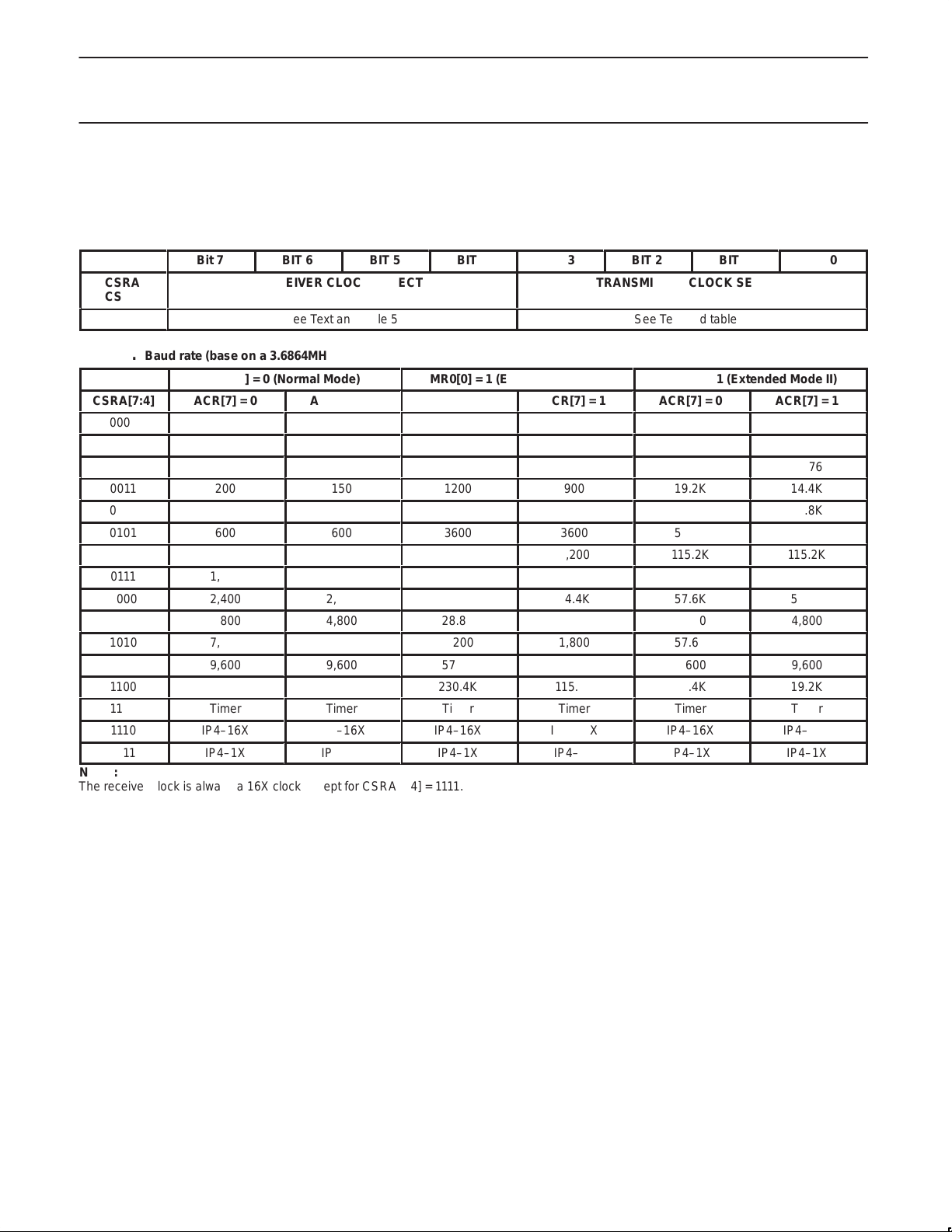
Philips Semiconductors Preliminary specification
Dual Universal Asynchronous
Receiver/Transmitter (DUART)
CSRA—Channel A Clock Select Register
CSRA[7:4]—Channel A Receiver Clock Select
This field selects the baud rate clock for the Channel A receiver. The field definition is shown in Table 5.
CSR CLOCK SELECT REGISTER
Bit 7
CSRA
CSRB
Table 5. Baud rate (base on a 3.6864MHz crystal clock)
MR0[0] = 0 (Normal Mode)
CSRA[7:4]
0000
0001
0010
0011
0100
0101
0110
0111
1000
1001
1010
1011
1100
1101
1110
1111
NOTE:
The receiver clock is always a 16X clock except for CSRA[7:4] = 1111.
ACR[7] = 0
50
110
134.5
200
300
600
1,200
1,050
2,400
4,800
7,200
9,600
38.4K
Timer
IP4–16X
IP4–1X
BIT 6
RECEIVER CLOCK SELECT
See Text and table 5
ACR[7] = 1
IP4–16X
IP4–1X
BIT 5
75
110
134.5
150
300
600
1,200
2,000
2,400
4,800
1,800
9,600
19.2K
Timer
BIT 4
MR0[0] = 1 (Extended Mode I)
ACR[7] = 0
300
110
134.5
1200
1800
3600
7200
1,050
14.4K
28.8K
7,200
57.6K
230.4K
Timer
IP4–16X
IP4–1X
BIT 3
ACR[7] = 1
450
110
134.5
900
1800
3600
7,200
2,000
14.4K
28.8K
1,800
57.6K
115.2K
Timer
IP4–16X
IP4–1X
BIT 2
TRANSMITTER CLOCK SELECT
SC28L92
BIT 1
See Text and table 5
MR0[2] = 1 (Extended Mode II)
ACR[7] = 0
4,800
880
1,076
19.2K
28.8K
57.6K
115.2K
1,050
57.6K
4,800
57.6K
9,600
38.4K
Timer
IP4–16X
IP4–1X
BIT 0
ACR[7] = 1
7,200
880
1,076
14.4K
28.8K
57.6K
115.2K
2,000
57.6K
4,800
14.4K
9,600
19.2K
Timer
IP4–16X
IP4–1X
1998 Oct 05
22
Page 23
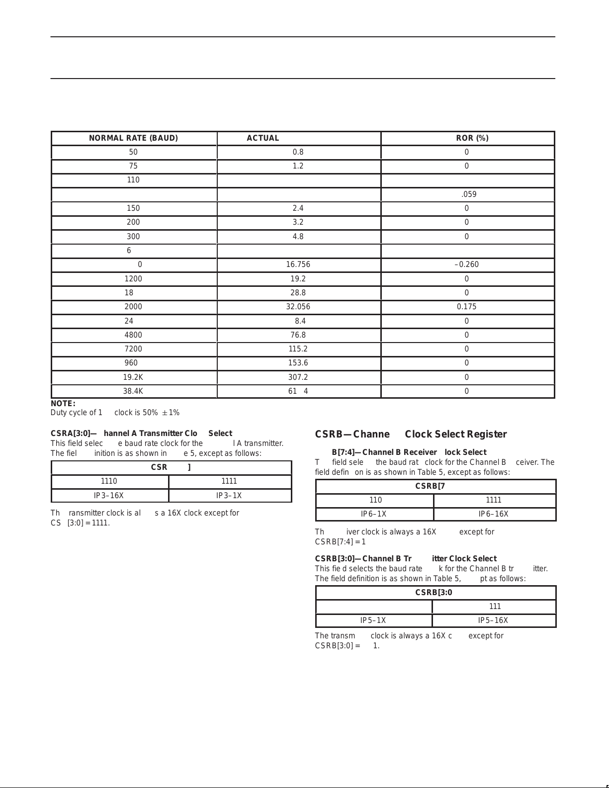
Philips Semiconductors Preliminary specification
БББББББББ
Dual Universal Asynchronous
Receiver/Transmitter (DUART)
Table 6. Bit rate generator characteristics
Crystal or Clock = 3.6864MHz
NORMAL RATE (BAUD)
50
75
110
134.5
150
200
300
600
1050
1200
1800
2000
2400
4800
7200
9600
19.2K
38.4K
NOTE:
Duty cycle of 16X clock is 50% 1%
ACTUAL 16X CLOCK (KHz)
0.8
1.2
1.759
2.153
2.4
3.2
4.8
9.6
16.756
19.2
28.8
32.056
38.4
76.8
115.2
153.6
307.2
614.4
SC28L92
ERROR (%)
0
0
–0.069
0.059
0
0
0
0
–0.260
0
0
0.175
0
0
0
0
0
0
CSRA[3:0]—Channel A Transmitter Clock Select
This field selects the baud rate clock for the Channel A transmitter.
The field definition is as shown in Table 5, except as follows:
CSRA[3:0]
1110
IP3–16X
The transmitter clock is always a 16X clock except for
CSR[3:0] = 1111.
1111
IP3–1X
CSRB—Channel B Clock Select Register
CSRB[7:4]—Channel B Receiver Clock Select
This field selects the baud rate clock for the Channel B receiver. The
field definition is as shown in Table 5, except as follows:
CSRB[7:4]
1110
IP6–1X
The receiver clock is always a 16X clock except for
CSRB[7:4] = 1111.
CSRB[3:0]—Channel B Transmitter Clock Select
This field selects the baud rate clock for the Channel B transmitter.
The field definition is as shown in Table 5, except as follows:
CSRB[3:0]
1110
IP5–1X
The transmitter clock is always a 16X clock except for
CSRB[3:0] = 1111.
1111
IP6–16X
1111
IP5–16X
1998 Oct 05
23
Page 24
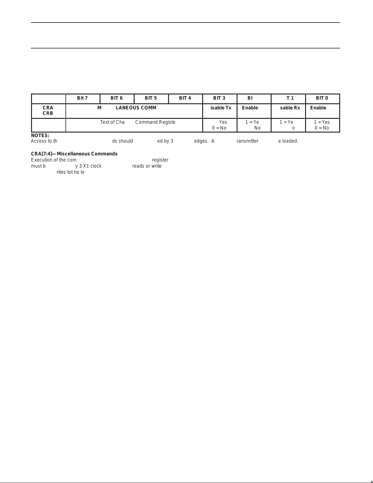
Philips Semiconductors Preliminary specification
Á
Á
Á
Á
Á
Á
Á
Á
Á
Á
Á
Á
Á
Dual Universal Asynchronous
BIT 1
0 = No
SC28L92
BIT 0
ÁÁÁ
Enable Rx
1 = Yes
0 = No
ÁÁÁ
or VDD.
SS
Receiver/Transmitter (DUART)
CRA—Channel A Command Register
CRA is a register used to supply commands to Channel A. Multiple commands can be specified in a single write to CRA as long as the
commands are non-conflicting, e.g., the ‘enable transmitter’ and ‘reset transmitter’ commands cannot be specified in a single command word.
CR COMMAND REGISTER
ÁÁÁÁÁÁ
Bit 7
CRA
CRB
See Text of Channel Command Register
ÁÁÁББББББББББББББ
NOTES:
Access to the miscellaneous commands should be separated by 3 X1 clock edges. A disabled transmitter cannot be loaded.
CRA[7:4]—Miscellaneous Commands
Execution of the commands in the upper four bits of this register
must be separated by 3 X1 clock edges. Other reads or writes
(including writes tot he lower four bits) may be inserted to achieve
this separation.
CRA[7:4]—Commands
0000 No command.
0001 Reset MR pointer. Causes the Channel A MR pointer to
point to MR1.
0010 Reset receiver. Resets the Channel A receiver as if a
hardware reset had been applied. The receiver is
disabled and the FIFO is flushed.
0011 Reset transmitter. Resets the Channel A transmitter as
if a hardware reset had been applied.
0100 Reset error status. Clears the Channel A Received
Break, Parity Error, and Overrun Error bits in the status
register (SRA[7:4]). Used in character mode to clear OE
status (although RB, PE and FE bits will also be
cleared) and in block mode to clear all error status after
a block of data has been received.
0101 Reset Channel A break change interrupt. Causes the
Channel A break detect change bit in the interrupt
status register (ISR[2]) to be cleared to zero
0110 Start break. Forces the TxDA output Low (spacing). If
the transmitter is empty the start of the break condition
will be delayed up to two bit times. If the transmitter is
active the break begins when transmission of the
character is completed. If a character is in the TxFIFO,
the start of the break will be delayed until that character,
or any other loaded subsequently are transmitted. The
transmitter must be enabled for this command to be
accepted.
0111 Stop break. The TxDA line will go High (marking) within
two bit times. TxDA will remain High for one bit time
before the next character, if any, is transmitted.
1000 Assert RTSN. Causes the RTSN output to be asserted
(Low).
1001 Negate RTSN. Causes the RTSN output to be negated
(High)
BIT 6
ÁÁÁ
BIT 5
ÁÁ
MISCELLANEOUS COMMANDS
BIT 4
ÁÁÁ
BIT 3
ÁÁÁ
Disable Tx
1 = Yes
0 = No
ÁÁÁ
BIT 2
ÁÁ
Enable Tx
1 = Yes
0 = No
ÁÁ
ÁÁÁ
Disable Rx
1 = Yes
ÁÁÁ
1010 Set Timeout Mode On. The receiver in this channel will
restart the C/T as each receive character is transferred
from the shift register to the RxFIFO. The C/T is placed
in the counter mode, the STAR T/STOP counter
commands are disabled, the counter is stopped, and
the Counter Ready Bit, ISR[3], is reset. (See also
Watchdog timer description in the receiver section.)
1011 Set MR pointer to ‘0’
1100 Disable Timeout Mode. This command returns control
of the C/T to the regular STAR T/STOP counter
commands. It does not stop the counter, or clear any
pending interrupts. After disabling the timeout mode, a
‘Stop Counter’ command should be issued to force a
reset of the ISR(3) bit
1101 Not used.
1110 Power Down Mode On. In this mode, the DUART
oscillator is stopped and all functions requiring this
clock are suspended. The execution of commands
other than disable power down mode (111 1) requires a
X1/CLK. While in the power down mode, do not issue
any commands to the CR except the disable power
down mode command. The contents of all registers will
be saved while in this mode. . It is recommended that
the transmitter and receiver be disabled prior to placing
the DUART into power down mode. This command is in
CRA only.
1111 Disable Power Down Mode. This command restarts the
oscillator. After invoking this command, wait for the
oscillator to start up before writing further commands to
the CR. This command is in CRA only. For maximum
power reduction input pins should be at V
CRA[3]—Disable Channel A Transmitter
This command terminates transmitter operation and reset the
TxDRY and TxEMT status bits. However, if a character is being
transmitted or if a character is in the TxFIFO when the transmitter is
disabled, the transmission of the character(s) is completed before
assuming the inactive state.
CRA[2]—Enable Channel A Transmitter
Enables operation of the Channel A transmitter. The TxRDY and
TxEMT status bits will be asserted if the transmitter is idle.
1998 Oct 05
24
Page 25

Philips Semiconductors Preliminary specification
Dual Universal Asynchronous
Receiver/Transmitter (DUART)
CRA[1]—Disable Channel A Receiver
This command terminates operation of the receiver immediately—a
character being received will be lost. The command has no effect on
the receiver status bits or any other control registers. If the special
multi-drop mode is programmed, the receiver operates even if it is
disabled. See Operation section.
CRA[0]—Enable Channel A Receiver
Enables operation of the Channel A receiver. If not in the special
wakeup mode, this also forces the receiver into the search for
start-bit state.
SC28L92
CRB—Channel B Command Register
CRB is a register used to supply commands to Channel B. Multiple
commands can be specified in a single write to CRB as long as the
commands are non-conflicting, e.g., the ‘enable transmitter’ and
‘reset transmitter’ commands cannot be specified in a single
command word.
The bit definitions for this register are identical to the bit definitions
for CRA, with the exception of commands “Ex” and “Fx” which are
used for power down mode. These two commands are not used in
CRB. All other control actions that apply to CRA also apply to CRB.
1998 Oct 05
25
Page 26
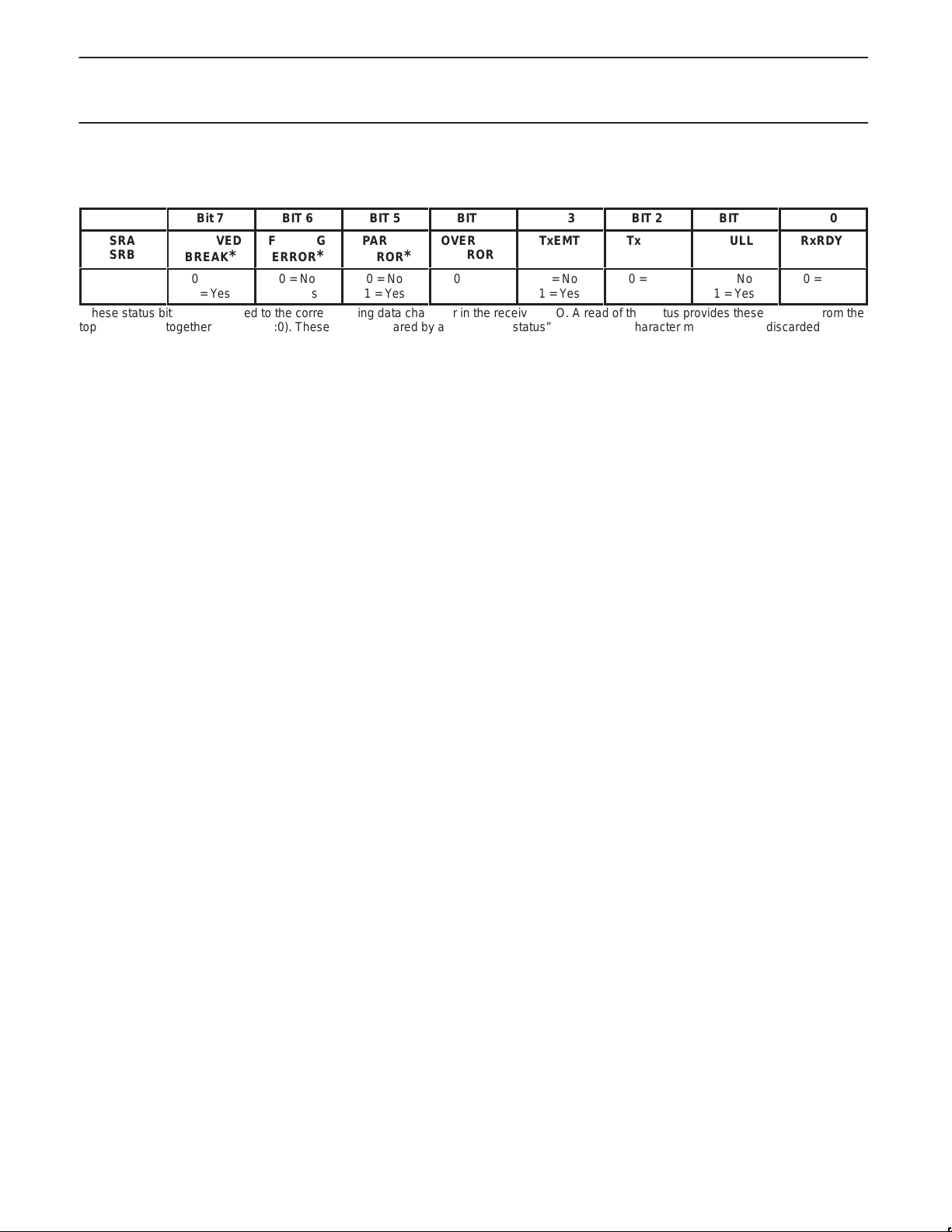
Philips Semiconductors Preliminary specification
Á
Á
Á
Á
Á
Á
Á
Á
Á
Dual Universal Asynchronous
BIT 1
0 = No
SC28L92
BIT 0
RxRDY
ÁÁÁ
0 = No
1 = Yes
Receiver/Transmitter (DUART)
SRA—Channel A Status Register
SR STATUS REGISTER
Bit 7
SRA
SRB
ÁÁ
RECEIVED
BREAK
ÁÁÁ
*
0 = No
1 = Yes
*These status bits are appended to the corresponding data character in the receive FIFO. A read of the status provides these bits (7:5) from the
top of the FIFO together with bits (4:0). These bits are cleared by a “reset error status” command. In character mode they are discarded when
the corresponding data character is read from the FIFO. In block error mode, the error-reset command (command 4x or receiver reset )must
used to clear block error conditions
SRA[7]—Channel A Received Break This bit indicates that an all zero character of the programmed length has been received without a stop bit. Only a single FIFO position is occupied when a break is received: further entries to the FIFO are inhibited until the RxDA line returns to the marking state for at least one-half a bit time two successive edges of the internal or external 1X clock. This will
usually require a high time of one X1 clock period or 3 X1
edges since the clock of the controller is not synchronous to
the X1 clock.
When this bit is set, the Channel A ‘change in break’ bit in the ISR
(ISR[2]) is set. ISR[2] is also set when the end of the break
condition, as defined above, is detected.
The break detect circuitry can detect breaks that originate in the
middle of a received character. However, if a break begins in the
middle of a character, it must persist until at least the end of the next
character time in order for it to be detected.
This bit is reset by command 4 (0100) written to the command
register or by receiver reset.
SRA[6]—Channel A Framing Error
This bit, when set, indicates that a stop bit was not detected when
the corresponding data character in the FIFO was received. The
stop bit check is made in the middle of the first stop bit position.
SRA[5]—Channel A Parity Error
This bit is set when the ‘with parity’ or ‘force parity’ mode is
programmed and the corresponding character in the FIFO was
received with incorrect parity.
In the special multi-drop mode the parity error bit stores the receive
A/D (Address/Data) bit.
SRA[4]—Channel A Overrun Error
This bit, when set, indicates that one or more characters in the
received data stream have been lost. It is set upon receipt of a new
character when the FIFO is full and a character is already in the
receive shift register waiting for an empty FIFO position. When this
occurs, the character in the receive shift register (and its break
detect, parity error and framing error status, if any) is lost.
This bit is cleared by a ‘reset error status’ command.
BIT 6
FRAMING
*
ERROR
ÁÁÁ
0 = No
1 = Yes
BIT 5
PARITY
ERROR
ÁÁ
0 = No
1 = Yes
*
ÁÁÁ
BIT 4
OVERRUN
ERROR
0 = No
1 = Yes
BIT 3
TxEMT
ÁÁÁ
0 = No
1 = Yes
BIT 2
TxRDY
ÁÁ
0 = No
1 = Yes
FFULL
ÁÁÁ
1 = Yes
SRA[3]—Channel A Transmitter Empty (TxEMTA)
This bit will be set when the transmitter under runs, i.e., both the
TxEMT and TxRDY bits are set. This bit and TxRDY are set when
the transmitter is first enabled and at any time it is re-enabled after
either (a) reset, or (b) the transmitter has assumed the disabled
state. It is always set after transmission of the last stop bit of a
character if no character is in the THR awaiting transmission.
It is reset when the THR is loaded by the CPU, a pending
transmitter disable is executed, the transmitter is reset, or the
transmitter is disabled while in the under run condition.
SRA[2]—Channel A Transmitter Ready (TxRDYA)
This bit, when set, indicates that the transmit FIFO is not full and
ready to be loaded with another character. This bit is cleared when
the transmit FIFO is loaded by the CPU and there are (after this
load) no more empty locations in the FIFO. It is set when a
character is transferred to the transmit shift register. TxRDYA is
reset when the transmitter is disabled and is set when the
transmitter is first enabled. Characters loaded to the TxFIFO while
this bit is 0 will be lost. This bit has different meaning from ISR[0].
SRA[1]—Channel A FIFO Full (FFULLA)
This bit is set when a character is transferred from the receive shift
register to the receive FIFO and the transfer causes the FIFO to
become full, i.e., all eight FIFO positions are occupied. It is reset
when the CPU reads the receive FIFO. If a character is waiting in
the receive shift register because the FIFO is full, FFULLA will not
be reset when the CPU reads the receive FIFO. This bit has
different meaning from ISR1 when MR1 6 is programmed to a ‘1’.
SRA[0]—Channel A Receiver Ready (RxRDY A)
This bit indicates that a character has been received and is waiting
in the FIFO to be read by the CPU. It is set when the character is
transferred from the receive shift register to the FIFO and reset
when the CPU reads the receive FIFO, only if (after this read) there
are no more characters in the FIFO.
SRB—Channel B Status Register
The bit definitions for this register are identical to the bit definitions
for SRA, except that all status applies to the Channel B receiver and
transmitter and the corresponding inputs and outputs.
1998 Oct 05
26
Page 27

Philips Semiconductors Preliminary specification
Dual Universal Asynchronous
Receiver/Transmitter (DUART)
OPCR—Output Port Configuration Register
OPCR OUTPUT PORT CONFIGURA TION REGISTER
Bit 7
OP7
0 = OPR[7]
1 = TxRDY B
OPCR[7]—OP7 Output Select
This bit programs the OP7 output to provide one of the following:
0 The complement of OPR[7].
1 The Channel B transmitter interrupt output which is the
complement of ISR[4]. When in this mode OP7 acts as an
open-drain output. Note that this output is not masked by the
contents of the IMR.
OPCR[6]—OP6 Output Select
This bit programs the OP6 output to provide one of the following:
0 The complement of OPR[6].
1 The Channel A transmitter interrupt output which is the
complement of ISR[0]. When in this mode OP6 acts as an
open-drain output. Note that this output is not masked by the
contents of the IMR.
OPCR[5]—OP5 Output Select
This bit programs the OP5 output to provide one of the following:
0 The complement of OPR[5].
1 The Channel B receiver interrupt output which is the
complement of ISR[5]. When in this mode OP5 acts as an
open-drain output. Note that this output is not masked by the
contents of the IMR.
OPCR[4]—OP4 Output Select
This field programs the OP4 output to provide one of the following:
0 The complement of OPR[4].
1 The Channel A receiver interrupt output which is the
complement of ISR[1]. When in this mode OP4 acts as an
open-drain output. Note that this output is not masked by the
contents of the IMR.
BIT 6
OP6
0 = OPR[6]
1 = TxRDY A
BIT 5
OP5
0 = OPR[5]
1 = RxRDY/FFULL B
1 = RxRDY/FFULL A
BIT 4
OP4
0 = OPR[4]
OPCR[3:2]—OP3 Output Select
This bit programs the OP3 output to provide one of the following:
00 The complement of OPR[3].
01 The counter/timer output, in which case OP3 acts as an
open-drain output. In the timer mode, this output is a square
wave at the programmed frequency. In the counter mode,
the output remains High until terminal count is reached, at
which time it goes Low. The output returns to the High state
when the counter is stopped by a stop counter command.
Note that this output is not masked by the contents of the
IMR.
10 The 1X clock for the Channel B transmitter, which is the
clock that shifts the transmitted data. If data is not being
transmitted, a free running 1X clock is output.
11 The 1X clock for the Channel B receiver, which is the clock
that samples the received data. If data is not being received,
a free running 1X clock is output.
OPCR[1:0]—OP2 Output Select
This field programs the OP2 output to provide one of the following:
00 The complement of OPR[2].
01 The 16X clock for the Channel A transmitter. This is the
clock selected by CSRA[3:0], and will be a 1X clock if
CSRA[3:0] = 1111.
10 The 1X clock for the Channel A transmitter, which is the
clock that shifts the transmitted data. If data is not being
transmitted, a free running 1X clock is output.
11 The 1X clock for the Channel A receiver, which is the clock
that samples the received data. If data is not being received,
a free running 1X clock is output.
BIT 3
OP3
00 = OPR[3]
01 = C/T OUTPUT
10 = TxCB(1X)
11 = RxCB(1X)
BIT 2
OP2
BIT 1
OP1
00 = OPR[2]
01 = TxCA(16X)
10 = TxCA(1X)
11 = RxCA(1X)
SC28L92
BIT 0
OP0
1998 Oct 05
27
Page 28

Philips Semiconductors Preliminary specification
Á
Á
Á
Á
Á
Á
Á
Á
Á
Dual Universal Asynchronous
BIT 1
OP 1
0 = no
BIT 1
OP 1
1=reset bit
0 = no
change
SC28L92
BIT 0
OP 0
1=set bit
ÁÁÁ
0 = no
change
BIT 0
OP 0
1=reset bit
0 = no
change
Receiver/Transmitter (DUART)
SOPR—Set the Output Port Bits (OPR)
SOPR[7:0]—Ones in the byte written to this register will cause the corresponding bit positions in the OPR to set to 1. Zeros have no effect. This
allows software to set individual bits with our keeping a copy of the OPR bit configuration.
Bit 7
OP 7
Set OPR
Bits
ÁÁ
1=set bit
ÁÁÁ
0 = no
change
ROPR—Reset Output Port Bits (OPR)
ROPR[7:0]—Ones in the byte written to the ROPR will cause the corresponding bit positions in the OPR to set to 0. Zeros have no effect. This
allows software to reset individual bits with our keeping a copy of the OPR bit configuration.
Bit 7
OP 7
Reset OPR
Bits
1=reset bit
0 = no
change
BIT 6
OP 6
1=set bit
ÁÁÁ
0 = no
change
BIT 6
OP 6
1=reset bit
0 = no
change
BIT 5
OP 5
1=set bit
ÁÁ
0 = no
change
BIT 5
OP 5
1=reset bit
0 = no
change
BIT 4
OP 4
1=set bit
ÁÁÁ
0 = no
change
BIT 4
OP 4
1=reset bit
0 = no
change
BIT 3
OP 3
1=set bit
ÁÁÁ
0 = no
change
BIT 3
OP 3
1=reset bit
0 = no
change
BIT 2
OP 2
1=set bit
ÁÁ
0 = no
change
BIT 2
OP 2
1=reset bit
0 = no
change
1=set bit
ÁÁÁ
change
OPR Output Port Register
The output pins (OP pins) drive the compliment of the data written to this register.
OPR
Bit 7
OP 7
0 = Pin High
1 = Pin Low
BIT 6
OP 6
0 = Pin High
1 = Pin Low
BIT 5
OP 5
0 = Pin High
1 = Pin Low
BIT 4
OP 4
0 = Pin High
1 = Pin Low
ACR Auxiliary Control Register
ACR
Bit 7
BRG SET
Select
0 = set 1
1 = set 2
BIT 6
BIT 5
Counter Timer Mode
Mode and clock sour select
See table 7
BIT 4
BIT 3
OP 3
0 = Pin High
1 = Pin Low
BIT 3
Delta IP3 int
enable
0 = off
1 = enabled
BIT 2
OP 2
0 = Pin High
1 = Pin Low
BIT 2
Delta IP3 int
enable
0 = off
1 = enabled
BIT 1
OP 1
0 = Pin High
1 = Pin Low
BIT 1
Delta IP3 int
enable
0 = off
1 = enabled
BIT 0
OP 0
0 = Pin High
1 = Pin Low
BIT 0
Delta IP3 int
enable
0 = off
1 = enabled
1998 Oct 05
28
Page 29

Philips Semiconductors Preliminary specification
Dual Universal Asynchronous
Receiver/Transmitter (DUART)
ACR—Auxiliary Control Register
ACR[7]—Baud Rate Generator Set Select
This bit selects one of two sets of baud rates to be generated by the
BRG (see Table 5).
The selected set of rates is available for use by the Channel A and
B receivers and transmitters as described in CSRA and CSRB.
Baud rate generator characteristics are given in Table 6.
ACR[6:4]—Counter/Timer Mode And Clock Source Select
This field selects the operating mode of the counter/timer and its
clock source as shown in Table 7
SC28L92
ACR [3:0]—IP3, IP2, IP1, IP0 Change-of-State Interrupt Enable
This field selects which bits of the input port change register (IPCR)
cause the input change bit in the interrupt status register (ISR [7]) to
be set. If a bit is in the ‘on’ state the setting of the corresponding bit
in the IPCR will also result in the setting of ISR [7], which results in
the generation of an interrupt output if IMR [7] = 1. If a bit is in the
‘off’ state, the setting of that bit in the IPCR has no effect on ISR [7].
1998 Oct 05
29
Page 30

Philips Semiconductors Preliminary specification
Á
Á
Á
Á
Á
Á
Á
Á
Á
Á
Á
Á
Á
Á
Á
Á
Á
Á
Á
Á
Á
Á
Dual Universal Asynchronous
Receiver/Transmitter (DUART)
Table 7. ACR 6:4 field definition
ACR
Á
6:4
000
001
010
011
100
101
110
111
Á
NOTE:
The timer mode generates a square wave
IPCR INPUT PORT CONFIGURATION REGISTER
ÁÁÁÁÁÁ
ÁÁÁÁÁÁ
IPCR
MODE
ÁÁ
Counter
Counter
Counter
Counter
Timer
Timer
Timer
Timer
ÁÁ
Delta IP3
1 = change
ББББББББББ
CLOCK SOURCE
External (IP2)
TxCA - 1X clock of Channel A transmitter
TxCB - 1X clock of Channel B transmitter
Crystal or external clock (X1/CLK) divided
by 16
External (IP2)
External (IP2) divided by 16
Crystal or external clock (X1/CLK)
Crystal or external clock (X1/CLK) divided
by 16
ББББББББББ
Bit 7
0 = no
change
BIT 6
ÁÁÁ
Delta IP3
0 = no
ÁÁÁ
change
1 = change
BIT 5
ÁÁ
Delta IP3
0 = no
ÁÁ
change
1 = change
BIT 4
ÁÁÁ
Delta IP3
0 = no
ÁÁÁ
change
1 = change
BIT 3
ÁÁÁ
IP 3
0 = low
ÁÁÁ
1 = High
BIT 2
ÁÁ
IP 2
0 = low
ÁÁ
1 = High
BIT 1
ÁÁÁ
IP 1
0 = low
ÁÁÁ
1 = High
SC28L92
BIT 0
ÁÁÁ
IP 0
0 = low
ÁÁÁ
1 = High
IPCR [7:4]—IP3, IP2, IP1, IP0 Change-of-State
These bits are set when a change-of-state, as defined in the input
port section of this data sheet, occurs at the respective input pins.
They are cleared when the IPCR is read by the CPU. A read of the
IPCR also clears ISR [7], the input change bit in the interrupt status
register. The setting of these bits can be programmed to generate
an interrupt to the CPU.
IPCR [3:0]—IP3, IP2, IP1, IP0 Change-of-State
These bits provide the current state of the respective inputs. The
information is unlatched and reflects the state of the input pins at the
time the IPCR is read.
1998 Oct 05
30
Page 31

Philips Semiconductors Preliminary specification
Á
Á
Á
Á
Á
Á
Á
Á
Á
Á
Á
Á
Á
Á
Á
Á
Á
Dual Universal Asynchronous
BIT 1
RxRDY/
FFULL A
ÁÁ
0 = not
enabled
ÁÁ
SC28L92
BIT 0
TxRDY A
ÁÁÁ
0 = not
enabled
ÁÁÁ
1 = enabled
Receiver/Transmitter (DUART)
ISR—Interrupt Status Register
This register provides the status of all potential interrupt sources. The contents of this register are masked by the Interrupt Mask Register (IMR).
If a bit in the ISR is a ‘1’ and the corresponding bit in the IMR is also a ‘1’, the INTRN output will be asserted (Low). If the corresponding bit in
the IMR is a zero, the state of the bit in the ISR has no effect on the INTRN output. Note that the IMR does not mask the reading of the ISR - the
true status will be provided regardless of the contents of the IMR. The contents of this register are initialized to H‘00’ when the DUART is reset.
ISR INTERRUPT STATUS REGISTER
Bit 7
ISR
ÁÁÁ
INPPUT
PORT
ÁÁ
CHANGE
0 = not
ÁÁÁÁÁÁ
enabled
1 = enabled
ISR[7]—Input Port Change Status
This bit is a ‘1’ when a change-of-state has occurred at the IP0, IP1,
IP2, or IP3 inputs and that event has been selected to cause an
interrupt by the programming of ACR[3:0]. The bit is cleared when
the CPU reads the IPCR.
ISR[6]—Channel B Change In Break
This bit, when set, indicates that the Channel B receiver has
detected the beginning or the end of a received break. It is reset
when the CPU issues a Channel B ‘reset break change interrupt’
command.
ISR[5]—RxB Interrupt
This bit indicates that the channel B receiver is interrupting
according to the fill level programmed by the MR0 and MR1
registers. This bit has a different meaning than the receiver
ready/full bit in the status register.
ISR[4]—TxB Interrupt
This bit indicates that the channel B transmitter is interrupting
according to the interrupt level programmed in the MR0[5:4] bits.
This bit has a different meaning than the Tx RDY bit in the status
register.
ISR[3]—Counter Ready.
In the counter mode, this bit is set when the counter reaches
terminal count and is reset when the counter is stopped by a stop
counter command.
BIT 6
DELTA
Break B
ÁÁÁ
0 = not
enabled
ÁÁÁ
1 = enabled
BIT 5
RxRDY/
FFULL B
ÁÁÁ
0 = not
enabled
ÁÁÁ
1 = enabled
BIT 4
TxRDY B
ÁÁ
0 = not
enabled
ÁÁ
1 = enabled
In the timer mode, this bit is set once each cycle of the generated
square wave (every other time that the counter/timer reaches zero
count). The bit is reset by a stop counter command. The command,
however, does not stop the counter/timer.
ISR[2]—Channel A Change in Break
This bit, when set, indicates that the Channel A receiver has
detected the beginning or the end of a received break. It is reset
when the CPU issues a Channel A ‘reset break change interrupt’
command.
ISR[1]—RxA Interrupt
This bit indicates that the channel A receiver is interrupting
according to the fill level programmed by the MR0 and MR1
registers. This bit has a different meaning than the receiver
ready/full bit in the status register.
ISR[0]—TxA Interrupt
This bit indicates that the channel A transmitter is interrupting
according to the interrupt level programmed in the MR0[5:4] bits.
This bit has a different meaning than the Tx RDY bit in the status
register.
BIT 3
Counter
Ready
ÁÁÁ
0 = not
enabled
ÁÁÁ
1 = enabled
BIT 2
Delta
Break A
ÁÁÁ
0 = not
enabled
ÁÁÁ
1 = enabled
1 = enabled
1998 Oct 05
31
Page 32

Philips Semiconductors Preliminary specification
Á
Á
Á
Á
Á
Á
Á
Á
Á
Á
Á
Á
Á
Á
Á
Á
Á
Á
Dual Universal Asynchronous
BIT 1
0 = not
BIT 1
SC28L92
BIT 0
TxRDY
A
ÁÁÁ
0 = not
enabled
ÁÁÁ
1 = enabled
BIT 0
Receiver/Transmitter (DUART)
IMR—Interrupt Mask Register
The programming of this register selects which bits in the ISR causes an interrupt output. If a bit in the ISR is a ‘1’ and the corresponding bit in
the IMR is also a ‘1’ the INTRN output will be asserted. If the corresponding bit in the IMR is a zero, the state of the bit in the ISR has no effect
on the INTRN output. Note that the IMR does not mask the programmable interrupt outputs OP3–OP7 or the reading of the ISR.
IMR INTERRUPT MASK REGISTER
Bit 7
IMR
ÁÁ
INTERRUPT
ÁÁ
INPPUT
PORT
ÁÁÁ
CHANGE
0 = not
enabled
ÁÁÁ
1 = enabled
CTPU and CTPL – Counter/Timer Registers
CTPU COUNTER TIMER PRESET UPPER
Bit 7
CTPU
CTPL COUNTER -TIMER PRESET LOW
Bit 7
CTPL
BIT 6
Delta
Break B
ÁÁÁ
0 = not
enabled
ÁÁÁ
1 = enabled
BIT 6
BIT 5
RxRDY/
FFULL B
ÁÁ
0 = not
enabled
ÁÁ
1 = enabled
BIT 5
BIT 4
TxRDY B
ÁÁÁ
0 = not
enabled
ÁÁÁ
1 = enabled
BIT 4
BIT 3
Counter
Ready
ÁÁÁ
0 = not
enabled
ÁÁÁ
1 = enabled
BIT 3
The lower eight (8) bits for the 16 bit counter timer preset register
BIT 6
BIT 5
BIT 4
BIT 3
BIT 2
The Upper eight (8) bits for the 16 bit counter timer preset register
BIT 2
Delta
Break A
ÁÁ
0 = not
enabled
ÁÁ
1 = enabled
BIT 2
BIT 1
RxRDY/
FFULL A
ÁÁÁ
enabled
ÁÁÁ
1 = enabled
BIT 0
The CTPU and CTPL hold the eight MSBs and eight LSBs,
respectively, of the value to be used by the counter/timer in either
the counter or timer modes of operation. The minimum value which
may be loaded into the CTPU/CTPL registers is H‘0002’. Note that
these registers are write-only and cannot be read by the CPU.
In the timer mode, the C/T generates a square wave whose period is
twice the value (in C/T clock periods) of the CTPU and CTPL. The
waveform so generated is often used for a data clock. The formula
for calculating the divisor n to load to the CTPU and CTPL for a
particular 1X data clock is shown below.
n = (C/T Clock Frequency) divided by (2 x 16 x Baud rate desired)
n = (C/T Clock Frequency)/ (2 x 16 x Baud rate desired)
Often this division will result in a non-integer number; 26.3, for
example. One can only program integer numbers in a digital divider.
Therefore, 26 would be chosen. This gives a baud rate error of
0.3/26.3 which is 1.14%; well within the ability asynchronous mode
of operation.
If the value in CTPU and CTPL is changed, the current half-period
will not be affected, but subsequent half periods will be. The C/T will
not be running until it receives an initial ‘Start Counter’ command
(read at address A3–A0 = 1110). After this, while in timer mode, the
C/T will run continuously. Receipt of a start counter command (read
with A3–A0 = 1110) causes the counter to terminate the current
timing cycle and to begin a new cycle using the values in CTPU and
CTPL.
The counter ready status bit (ISR[3]) is set once each cycle of the
square wave. The bit is reset by a stop counter command (read with
A3–A0 = H’F’). The command however, does not stop the C/T. The
generated square wave is output on OP3 if it is programmed to be
the C/T output. In the counter mode, the value C/T loaded into
CTPU and CTPL by the CPU is counted down to 0.. Counting
begins upon receipt of a start counter command. Upon reaching
terminal count H‘0000’, the counter ready interrupt bit (ISR[3]) is set.
The counter continues counting past the terminal count until stopped
by the CPU. If OP3 is programmed to be the output of the C/T, the
output remains High until terminal count is reached, at which time it
goes Low. The output returns to the High state and ISR[3] is cleared
when the counter is stopped by a stop counter command. The CPU
may change the values of CTPU and CTPL at any time, but the new
count becomes effective only on the next start counter commands. If
new values have not been loaded, the previous count values are
preserved and used for the next count cycle.
In the counter mode, the current value of the upper and lower 8 bits
of the counter (CTU, CTL) may be read by the CPU. It is
recommended that the counter be stopped when reading to prevent
potential problems which may occur if a carry from the lower 8 bits
to the upper 8 bits occurs between the times that both halves of the
counter are read. However, note that a subsequent start counter
command will cause the counter to begin a new count cycle using
the values in CTPU and CTPL.
When the C/T clock divided by 16 is selected, the maximum divisor
becomes 1,048,575.
Output Port Notes
The output ports are controlled from four places: the OPCR
register,the OPR register, the MR registers and the command
register (except the 2681 and 68681) The OPCR register controls
the source of the data for the output ports OP2 through OP7. The
data source for output ports OP0 and OP1 is controlled by the MR
and CR registers. When the OPR is the source of the data for the
output ports, the data at the ports is inverted from that in the OPR
register. The content of the OPR register is controlled by the “Set
Output Port Bits Command” and the “Reset Output Bits Command”.
These commands are at E and F, respectively. When these
commands are used, action takes place only at the bit locations
where ones exist. For example, a one in bit location 5 of the data
word used with the “Set Output Port Bits” command will result in
OPR5 being set to one. The OP5 would then be set to zero (V
SS ).
1998 Oct 05
32
Page 33

Philips Semiconductors Preliminary specification
Dual Universal Asynchronous
Receiver/Transmitter (DUART)
Similarly , a one in bit position 5 of the data word associated with the
“Reset Output Ports Bits” command would set OPR5 to zero and,
hence, the pin OP5 to a one (V
The CTS, RTS, CTS Enable Tx signals
CTS (Clear To Send) is usually meant to be a signal to the
transmitter meaning that it may transmit data to the receiver. The
CTS input is on pin IP0 for TxA and on IP1 for TxB. The CTS signal
is active low; thus, it is called CTSAN for TxA and CTSBN for TxB.
RTS is usually meant to be a signal from the receiver indicating that
the receiver is ready to receive data. It is also active low and is,
thus, called RTSAN for RxA and RTSBN for RxB. RTSAN is on pin
OP0 and RTSBN is on OP1. A receiver’s RTS output will usually be
connected to the CTS input of the associated transmitter. Therefore,
one could say that RTS and CTS are different ends of the same
wire!
DD
).
RESETN
Figure 2. Reset Timing (80XXX mode)
SC28L92
MR2(4) is the bit that allows the transmitter to be controlled by the
CTS pin (IP0 or IP1). When this bit is set to one AND the CTS input
is driven high, the transmitter will stop sending data at the end of the
present character being serialized. It is usually the RTS output of
the receiver that will be connected to the transmitter’s CTS input.
The receiver will set RTS high when the receiver FIFO is full AND
the start bit of the ninth character is sensed. Transmission then
stops with nine valid characters in the receiver. When MR2(4) is set
to one, CTSN must be at zero for the transmitter to operate. If
MR2(4) is set to zero, the IP pin will have no effect on the operation
of the transmitter. MR1(7) is the bit that allows the receiver to
control OP0. When OP0 (or OP1) is controlled by the receiver, the
meaning of that pin will be.
t
RES
SD00133
A0–A3
CEN
RDN
D0–D7
(READ)
WDN
D0–D7
(WRITE)
t
AS
t
AH
t
CS
t
RW
t
DD
FLOAT FLOATVALID
NOT
VALID
t
DS
VALID
Figure 3. Bus Timing (80XXX mode)
t
CH
t
RWD
t
DF
t
RWD
t
DH
SD00087
1998 Oct 05
33
Page 34

Philips Semiconductors Preliminary specification
Dual Universal Asynchronous
Receiver/Transmitter (DUART)
RESETN
t
RES
SD00109
Figure 4. Reset Timing (68XXX mode)
X1/CLK
A1–A4
RWN
CSN
D0–D7
DTACKN
t
DA
t
AS
t
t
RWS
t
DD
NOT
VALID
CSC
t
AH
t
DAL
DATA VALID
t
DCR
t
CSD
t
DAT
t
CSW
t
RWH
t
DF
t
DAH
SC28L92
NOTE: DACKN low requires two rising edges of X1 clock after CSN is low.
Figure 5. Bus Timing (Read Cycle) (68XXX mode)
t
CSC
X1/CLK
A1–A4
RWN
CSN
D0–D7
DTACKN
NOTE: DACKN low requires two rising edges of X1 clock after CSN is low.
t
AS
t
RWS
t
DS
Figure 6. Bus Timing (Write Cycle) (68XXX mode)
SD00147
t
RWH
t
t
DAT
CSW
t
DH
t
DAH
SD00148
t
AH
t
CSD
t
DCW
1998 Oct 05
34
Page 35

Philips Semiconductors Preliminary specification
Dual Universal Asynchronous
Receiver/Transmitter (DUART)
t
X1/CLK
INTRN
IACKN
D0–D7
DTACKN
NOTE: DACKN low requires two rising edges of X1 clock after CSN is low.
Figure 7. Interrupt Cycle Timing (68XXX mode)
CSC
t
DD
t
DAL
t
DCR
t
CSD
t
DAH
t
DAT
SC28L92
t
DF
SD00149
RDN
IP0–IP6
(a) INPUT PINS
WRN
OP0–OP7
(b) OUTPUT PINS
t
PS
OLD DATA NEW DATA
t
PH
t
PD
SD00135
Figure 8. Port Timing
1998 Oct 05
35
Page 36

Philips Semiconductors Preliminary specification
Dual Universal Asynchronous
Receiver/Transmitter (DUART)
V
WRN
OUTPUT
RDN
OUTPUT
1
V
M
1
INTERRUPT
INTERRUPT
NOTES:
1. INTRN or OP3-OP7 when used as interrupt outputs.
2. The test for open-drain outputs is intended to guarantee switching of the output transistor. Measurement of this response is referenced from the midpoint of the switching
, to a point 0.5V above VOL. This point represents noise margin that assures true switching has occurred. Beyond this level, the effects of external circuitry and
signal, V
M
test environment are pronounced and can greatly affect the resultant measurement.
Figure 9. Interrupt Timing (80xxx mode)
M
t
IR
V
+0.5V
OL
V
OL
t
IR
V
+0.5V
OL
V
OL
SC28L92
SD00136
t
CLK
t
CTC
t
Rx
t
X1/CLK
CTCLK
RxC
TxC
C1 = C2 ∼ 24pF FOR CL = 20pF
C1 and C2 should be chosen according to the crystal manufacturer’s specification.
C1 and C2 values will include any parasitic capacitance of the wiring and X1 X2 pins.
Gain at 3.6864MHz: 9 to 13 dB
Phase at 3.6864MHz: 272 to 276 degrees.
Package capacitance approximately 4pF.
Tx
t
CLK
t
CTC
t
Rx
t
Tx
X1
3pF
3pF
C1
C2
X2
3.6864MHz
2pF
4pF
Figure 10. Clock Timing
+5V
NOTE:
RESISTOR REQUIRED
FOR TTL INPUT.
CLK
*NOTE: X2 MUST BE LEFT OPEN.
SC26C92
50kΩ
to
100kΩ
470Ω
X1
X2*
TO UART
CIRCUIT
SD00154
1998 Oct 05
36
Page 37

Philips Semiconductors Preliminary specification
Dual Universal Asynchronous
Receiver/Transmitter (DUART)
TxC
(INPUT)
TxD
TxC
(1X OUTPUT)
Figure 11. Transmitter External Clocks
1 BIT TIME
(1 OR 16 CLOCKS)
t
TXD
t
TCS
SC28L92
SD00138
TxD D1 D2 D3 D4 D6BREAK
TRANSMITTER
ENABLED
TxRDY
(SR2)
WRN
1
CTSN
(IP0)
2
RTSN
(OP0)
NOTES:
1. Timing shown for MR2(4) = 1.
2. Timing shown for MR2(5) = 1.
RxC
(1X INPUT)
RxD
t
RXS
t
RXH
SD00139
Figure 12. Receiver External Clock
D1 D8 D9 D10 D12START
OPR(0) = 1 OPR(0) = 1
BREAK
STOP
BREAK
D11 WILL
NOT BE
WRITTEN TO
THE TxFIFO
Figure 13. Transmitter Timing
SD00155
1998 Oct 05
37
Page 38

Philips Semiconductors Preliminary specification
Dual Universal Asynchronous
Receiver/Transmitter (DUART)
RxD
RECEIVER
ENABLED
RxRDY
(SR0)
FFULL
(SR1)
RxRDY/
FFULL
2
(OP5)
RDN
OVERRUN
(SR4) RESET BY COMMAND
1
RTS
(OP0)
NOTES:
1. Timing shown for MR1(7) = 1.
2. Shown for OPCR(4) = 1 and MR(6) = 0.
D1 D2 D8 D9 D10 D11 D12 D13
STATUS DATA
D1
OPR(0) = 1
D11 WILL BE LOST
DUE TO OVERRUN
Figure 14. Receiver Timing
D12, D13 WILL BE LOST
DUE TO RECEIVER DISABLE.
STATUS DATAD2STATUS DATAD3STATUS DATA
D10
SC28L92
SD00156
TxD
TRANSMITTER
ENABLED
TxRDY
(SR2)
WRN
RxD
RECEIVER
ENABLED
RxRDY
(SR0)
RDN/WRN
MASTER STATION
MR1(4–3) = 11
MR1(2) = 1
PERIPHERAL STATION
MR1(4–3) = 11
BIT 9
1
ADD#1
ADD#1MR1(2) = 0 D0 MR1(2) = 1 ADD#2
BIT 9
0
BIT 9
ADD#1 1
D0 0
ADD#1
BIT 9
BIT 9
D0 0
STATUS DATA
D0
Figure 15. Wake-Up Mode
ADD#2 1
ADD#2 1
BIT 9
BIT 9
BIT 9
0
STATUS DATA
ADD#2
SD00096
1998 Oct 05
38
Page 39

Philips Semiconductors Preliminary specification
Dual Universal Asynchronous
Receiver/Transmitter (DUART)
INTRN
D0–D7
TxDA/B
OP0–OP7
50pF
150pF
Figure 16. Test Conditions on Outputs
2.7K
+5V
I = 2.4mA V
I = 400µA V
OL
OH
SC28L92
+5V
SD00157
1998 Oct 05
39
Page 40

Philips Semiconductors Preliminary specification
Dual Universal Asynchronous
Receiver/Transmitter (DUART)
PLCC44: plastic leaded chip carrier; 44 leads SOT187-2
SC28L92
1998 Oct 05
40
Page 41

Philips Semiconductors Preliminary specification
Dual Universal Asynchronous
Receiver/Transmitter (DUART)
QFP44: plastic quad flat package; 44 leads (lead length 1.3 mm); body 10 x 10 x 1.75 mm SOT307-2
SC28L92
1998 Oct 05
41
Page 42

Philips Semiconductors Preliminary specification
Dual Universal Asynchronous
Receiver/Transmitter (DUART)
Data sheet status
Data sheet
status
Objective
specification
Preliminary
specification
Product
specification
Product
status
Development
Qualification
Production
Definition
This data sheet contains the design target or goal specifications for product development.
Specification may change in any manner without notice.
This data sheet contains preliminary data, and supplementary data will be published at a later date.
Philips Semiconductors reserves the right to make chages at any time without notice in order to
improve design and supply the best possible product.
This data sheet contains final specifications. Philips Semiconductors reserves the right to make
changes at any time without notice in order to improve design and supply the best possible product.
[1]
SC28L92
[1] Please consult the most recently issued datasheet before initiating or completing a design.
Definitions
Short-form specification — The data in a short-form specification is extracted from a full data sheet with the same type number and title. For
detailed information see the relevant data sheet or data handbook.
Limiting values definition — Limiting values given are in accordance with the Absolute Maximum Rating System (IEC 134). Stress above one
or more of the limiting values may cause permanent damage to the device. These are stress ratings only and operation of the device at these or
at any other conditions above those given in the Characteristics sections of the specification is not implied. Exposure to limiting values for extended
periods may affect device reliability.
Application information — Applications that are described herein for any of these products are for illustrative purposes only. Philips
Semiconductors make no representation or warranty that such applications will be suitable for the specified use without further testing or
modification.
Disclaimers
Life support — These products are not designed for use in life support appliances, devices or systems where malfunction of these products can
reasonably be expected to result in personal injury . Philips Semiconductors customers using or selling these products for use in such applications
do so at their own risk and agree to fully indemnify Philips Semiconductors for any damages resulting from such application.
Right to make changes — Philips Semiconductors reserves the right to make changes, without notice, in the products, including circuits, standard
cells, and/or software, described or contained herein in order to improve design and/or performance. Philips Semiconductors assumes no
responsibility or liability for the use of any of these products, conveys no license or title under any patent, copyright, or mask work right to these
products, and makes no representations or warranties that these products are free from patent, copyright, or mask work right infringement, unless
otherwise specified.
Philips Semiconductors
811 East Arques Avenue
P.O. Box 3409
Sunnyvale, California 94088–3409
Telephone 800-234-7381
Copyright Philips Electronics North America Corporation 1998
All rights reserved. Printed in U.S.A.
Date of release: 10-98
Document order number: 9397 750 04465
1998 Oct 05
42
Page 43

INTEGRATED CIRCUITS
SC28L92
Dual Universal Asynchronous
Receiver/Transmitter (DUART)
Preliminary specification
IC19 Data Handbook
1998 Oct 05
Page 44

Philips Semiconductors Preliminary specification
Dual Universal Asynchronous
Receiver/Transmitter (DUART)
DESCRIPTION
The SC28L92 is a pin and function replacement for the SCC2692
and SC26C92 operating at 3.3 or 5 volts supply with added features
and deeper FIFOs. Its configuration on power up is that of the 2692.
Its differences from the 2692 are: 16 character receiver, 16
character transmit FIFOs, watch dog timer for each receiver, mode
register 0 is added, extended baud rate and overall faster speeds,
programmable receiver and transmitter interrupts. (Neither the
SC26C92 nor The SCC2692 is being discontinued.)
Pin programming will allow the device to operate with either the
Motorola or Intel bus interface The bit 3 of the MR0a register allows
the device to operate in an 8 byte FIFO mode if strict compliance
with the SC26C92 FIFO structure is required
The Philips Semiconductors SC28L92 Dual Universal Asynchronous
Receiver/Transmitter (DUART) is a single-chip CMOS-LSI
communications device that provides two full-duplex asynchronous
receiver/transmitter channels in a single package. It interfaces
directly with microprocessors and may be used in a polled or
interrupt driven system.
The operating mode and data format of each channel can be
programmed independently. Additionally , each receiver and
transmitter can select its operating speed as one of eighteen fixed
baud rates; a 16X clock derived from a programmable counter/timer,
or an external 1X or 16X clock. The baud rate generator and
counter/timer can operate directly from a crystal or from external
clock inputs. The ability to independently program the operating
speed of the receiver and transmitter make the DUART particularly
attractive for dual-speed channel applications such as clustered
terminal systems.
Each receiver and transmitter is buffered by 8 or 16 character FIFOs
to minimize the potential of receiver overrun, transmitter underpin
and to reduce interrupt overhead in interrupt driven systems. In
addition, a flow control capability is provided to disable a remote
transmitter when the receiver buffer is full.
Also provided on the SC28L92 are a multipurpose 7-bit input port
and a multipurpose 8-bit output port. These can be used as general
purpose I/O ports or can be assigned specific functions (such as
clock inputs or status/interrupt outputs) under program control.
The SC28L92 is available in two package versions: a 44-pin PLCC
and 44-pin plastic quad flat pack (PQFP).
FEATURES
•3.3 or 5.0 volt operation
•Dual full-duplex independent asynchronous receiver/transmitters
•16 character FIFOs for each receiver and transmitter
•Pin programming for 68K or 80xxx bus interface
•Programmable data format
– 5 to 8 data bits plus parity
– Odd, even, no parity or force parity
SC28L92
– - 1, 1.5 or 2 stop bits programmable in 1/16-bit increments
•16-bit programmable Counter/Timer
•Programmable baud rate for each receiver and transmitter
selectable from:
– 23 fixed rates: 50 to 230.4k baud
– Other baud rates to MHz at 16X
– Programmable user-defined rates derived from a programmable
counter/timer
– External 1X or 16X clock
•Parity, framing, and overrun error detection
•False start bit detection
•Line break detection and generation
•Programmable channel mode
– Normal (full-duplex)
– Automatic echo
– Local loop back
– Remote loop back
– Multi-drop mode (also called ‘wake-up’ or ‘9-bit’)
•Multi-function 7-bit input port
– Can serve as clock or control inputs
– Change of state detection on four inputs
– Inputs have typically >100k pull-up resistors
•Multi-function 8-bit output port
– Individual bit set/reset capability
– Outputs can be programmed to be status/interrupt signals
•Versatile interrupt system
– Single interrupt output with eight maskable interrupting
conditions
– Output port can be configured to provide a total of up to six
separate interrupt outputs that may be wire ORed.
– Each FIFO can be programmed for four different interrupt levels
– Watch dog timer for each receiver
•Maximum data transfer rates:
1X – 1Mb/sec, 16X – 1Mb/sec
•Automatic wake-up mode for multi-drop applications
•Start-end break interrupt/status
•Detects break which originates in the middle of a character
•On-chip crystal oscillator
•Power down mode
•Receiver time-out mode
•Single +3.3V or +5V power supply
•Powers up to emulate SCC2692 and S26C92
1998 Oct 05
2
Page 45

Philips Semiconductors Preliminary specification
Dual Universal Asynchronous
Receiver/Transmitter (DUART)
ORDERING INFORMATION
DESCRIPTION
44-Pin Plastic Leaded Chip Carrier (PLCC)
44-Pin Plastic Quad Flat Pack (PQFP)
INDUSTRIAL
VCC = +3.3 +5V ±10%,
TA = –40 to +85°C
SC28L92A1A
SC28L92A1B
SC28L92
DRAWING NUMBER
SOT187–2
SOT307-2
1998 Oct 05
3
Page 46

Philips Semiconductors Preliminary specification
Dual Universal Asynchronous
Receiver/Transmitter (DUART)
PIN CONFIGURATION DIAGRAM
80XXX PIN CONFIGURA TION
44 34
1
PQFP
11
12 22
Pin Function
1A3
2 IP0
3 WRN
4 RDN
5 RxDB
6 TxDB
7 OP1
8 OP3
9 OP5
10 OP7
11 I/M
12 D1
13 D3
14 D5
15 D7
Pin Function
16 GND
17 GND
18 INTRN
19 D6
20 D4
21 D2
22 D0
23 NC
24 OP6
25 OP4
26 OP2
27 OP0
28 TxDA
29 RxDA
30 x1/clk
Pin Function
31 x2
32 RESET
33 CEN
34 IP2
35 IP6
36 IP5
37 IP4
38 V
39 V
40 A0
41 IP3
42 A1
43 IP1
44 A2
SC28L92
6
7
33
23
Pin Function
1NC
2A0
3 IP3
4A1
5 IP1
6A2
CC
CC
SD00671
7A3
8 IP0
9 WRN
10 RDN
11 RxDB
12 I/M
13 TxDB
14 OP1
15 OP3
17
18
1
PLCC
Pin Function
16 OP5
17 OP7
18 D1
19 D3
20 D5
21 D7
22 V
23 NC
24 INTRN
25 D6
26 D4
27 D2
28 D0
29 OP6
30 OP4
40
39
29
28
Pin Function
31 OP2
32 OP0
33 TxDA
34 NC
35 RxDA
36 X1/CLK
SS
37 X2
38 RESET
39 CEN
40 IP2
41 IP6
42 IP5
43 IP4
44 V
CC
SD00672
1998 Oct 05
4
Page 47

Philips Semiconductors Preliminary specification
Dual Universal Asynchronous
Receiver/Transmitter (DUART)
PIN CONFIGURATION DIAGRAM
68XXX PIN CONFIGURA TION
44 34
1
PQFP
11
12 22
Pin Function
1A3
2 IP0
3 R/WN
4 DACKN
5 RxDB
6 TxDB
7 OP1
8 OP3
9 OP5
10 OP7
11 I/M
12 D1
13 D3
14 D5
15 D7
Pin Function
16 GND
17 GND
18 INTRN
19 D6
20 D4
21 D2
22 D0
23 NC
24 OP6
25 OP4
26 OP2
27 OP0
28 TxDA
29 RxDA
30 x1/clk
Pin Function
31 x2
32 RESETN
33 CSN
34 IP2
35 IACKN
36 IP5
37 IP4
38 V
39 V
40 A0
41 IP3
42 A1
43 IP1
44 A2
SC28L92
6
7
33
23
Pin Function
1NC
2A0
3 IP3
4A1
5 IP1
6A2
CC
CC
SD00673
7A3
8 IP0
9 R/WN
10 DACKN
11 RxDB
12 I/M
13 TxDB
14 OP1
15 OP3
17
18
1
PLCC
Pin Function
16 OP5
17 OP7
18 D1
19 D3
20 D5
21 D7
22 V
23 NC
24 INTRN
25 D6
26 D4
27 D2
28 D0
29 OP6
30 OP4
40
39
29
28
Pin Function
31 OP2
32 OP0
33 TxDA
34 NC
35 RxDA
36 X1/CLK
SS
37 X2
38 RESETN
39 CEN
40 IP2
41 IACKN
42 IP5
43 IP4
44 V
CC
SD00674
1998 Oct 05
5
Page 48

Philips Semiconductors Preliminary specification
Dual Universal Asynchronous
Receiver/Transmitter (DUART)
8
D0–D7
RDN
WRN
CEN
A0–A3
RESET
INTRN
4
BUS BUFFER
OPERATION CONTROL
ADDRESS
DECODE
R/W CONTROL
INTERRUPT CONTROL
IMR
ISR
CHANNEL A
8 BYTE TRANSMIT
FIFO
TRANSMIT
SHIFT REGISTER
8 BYTE RECEIVE
FIFO
WATCH DOG TIMER
RECEIVE SHIFT
REGISTER
MRA0, 1, 2
CRA
SRA
CHANNEL B
(AS ABOVE)
SC28L92
TxDA
RxDA
TxDB
RxDB
X1/CLK
INPUT PORT
TIMING
BAUD RATE
GENERATOR
CLOCK
SELECTORS
COUNTER/
TIMER
X2
XTAL OSC
CSRA
CSRB
ACR
U
CTPL
CTPL
CONTROL
TIMING
INTERNAL DATABUS
CHANGE OF
STATE
DETECTORS (4)
IPCR
ACR
OUTPUT PORT
FUNCTION
SELECT LOGIC
OPCR
OPR
7
8
IP0-IP6
OP0-OP7
V
CC
V
SS
SD00153
Figure 1. Block Diagram
1998 Oct 05
6
Page 49

Philips Semiconductors Preliminary specification
Á
Á
Á
Á
Á
Á
Á
Á
Á
Á
Á
Á
Á
Á
Á
Á
Á
Á
Á
Á
Á
Á
Á
Á
Á
Á
Á
Á
Á
Á
Á
Á
Á
Dual Universal Asynchronous
Receiver/Transmitter (DUART)
PIN CONFIGURATION FOR 80XXX BUS INTERFACE (INTEL)
ÁÁ
SYMBOL
I/M
D0–D7
CEN
ÁÁ
WRN
ÁÁ
RDN
A0–A3
RESET
ÁÁ
INTRN
ÁÁ
X1/CLK
X2
ÁÁ
RxDA
RxDB
TxDA
ÁÁ
TxDB
OP0
ÁÁ
OP1
OP2
OP3
ÁÁ
OP4
OP5
OP6
OP7
IP0
IP1
IP2
IP3
ÁÁ
IP4
IP5
ÁÁ
IP6
V
CC
GND
PIN
Á
TYPE
I
I/O
I
Á
I
Á
I
I
I
Á
O
Á
I
O
Á
I
I
O
Á
O
O
Á
O
O
O
Á
O
O
O
O
I
I
I
I
Á
I
I
Á
I
Pwr
Pwr
БББББББББББББББББББББББББББ
NAME AND FUNCTION
Bus Configuration: When high or not connected configures the bus interface to the Conditions shown in this table.
Data Bus: Bi-directional 3-State data bus used to transfer commands, data and status between the DUART and the
CPU. D0 is the least significant bit.
Chip Enable: Active-Low input signal. When Low, data transfers between the CPU and the DUART are enabled on
D0–D7 as controlled by the WRN, RDN and A0–A3 inputs. When High, places the D0–D7 lines in the 3-State
БББББББББББББББББББББББББББ
condition.
Write Strobe: When Low and CEN is also Low, the contents of the data bus is loaded into the addressed register. The
БББББББББББББББББББББББББББ
transfer occurs on the rising edge of the signal.
Read Strobe: When Low and CEN is also Low, causes the contents of the addressed register to be presented on the
data bus. The read cycle begins on the falling edge of RDN.
Address Inputs: Select the DUART internal registers and ports for read/write operations.
Reset: A High level clears internal registers (SRA, SRB, IMR, ISR, OPR, OPCR), puts OP0–OP7 in the High state,
stops the counter/timer, and puts Channels A and B in the inactive state, with the TxDA and TxDB outputs in the mark
БББББББББББББББББББББББББББ
(High) state. Sets MR pointer to MR1.
Interrupt Request: Active-Low, open-drain, output which signals the CPU that one or more of the eight maskable
interrupting conditions are true.
БББББББББББББББББББББББББББ
Crystal 1: Crystal or external clock input. A crystal or clock of the specified limits must be supplied at all times. When a
crystal is used, a capacitor must be connected from this pin to ground (see Figure 7).
Crystal 2: Connection for other side of the crystal. When a crystal is used, a capacitor must be connected from this pin
to ground (see Figure 7). If X1/CLK is driven from an external source, this pin must be left open.
БББББББББББББББББББББББББББ
Channel A Receiver Serial Data Input: The least significant bit is received first. “Mark” is High; “space” is Low.
Channel B Receiver Serial Data Input: The least significant bit is received first. “Mark” is High; “space” is Low.
Channel A Transmitter Serial Data Output: The least significant bit is transmitted first. This output is held in the “mark”
БББББББББББББББББББББББББББ
condition when the transmitter is disabled, idle or when operating in local loop back mode. “Mark” is High; “space” is Low.
Channel B Transmitter Serial Data Output: The least significant bit is transmitted first. This output is held in the ‘mark’
condition when the transmitter is disabled, idle, or when operating in local loop back mode. ‘Mark’ is High; ‘space’ is Low.
Output 0: General purpose output or Channel A request to send (RTSAN, active-Low). Can be deactivated
automatically on receive or transmit.
БББББББББББББББББББББББББББ
Output 1: General-purpose output or Channel B request to send (RTSBN, active-Low). Can be deactivated
automatically on receive or transmit.
Output 2: General purpose output, or Channel A transmitter 1X or 16X clock output, or Channel A receiver 1X clock output.
Output 3: General purpose output or open-drain, active-Low counter/timer output or Channel B transmitter 1X clock
output, or Channel B receiver 1X clock output.
БББББББББББББББББББББББББББ
Output 4: General purpose output or Channel A open-drain, active-Low, RxA interrupt ISR[1] output.
Output 5: General-purpose output or Channel B open-drain, active-Low, RxB interrupt ISR[5] output.
Output 6: General purpose output or Channel A open-drain, active-Low, TxA interrupt ISR[0] output.
Output 7: General-purpose output, or Channel B open-drain, active-Low, TxB interrupt ISR[4] output.
Input 0: General purpose input or Channel A clear to send active-Low input (CTSAN).
Input 1: General purpose input or Channel B clear to send active-Low input (CTSBN).
Input 2: General-purpose input or counter/timer external clock input.
Input 3: General purpose input or Channel A transmitter external clock input (TxCA). When the external clock is used
БББББББББББББББББББББББББББ
by the transmitter, the transmitted data is clocked on the falling edge of the clock.
Input 4: General purpose input or Channel A receiver external clock input (RxCA). When the external clock is used by
the receiver, the received data is sampled on the rising edge of the clock.
Input 5: General purpose input or Channel B transmitter external clock input (TxCB). When the external clock is used
БББББББББББББББББББББББББББ
by the transmitter, the transmitted data is clocked on the falling edge of the clock.
Input 6: General purpose input or Channel B receiver external clock input (RxCB). When the external clock is used by
the receiver, the received data is sampled on the rising edge of the clock.
Power Supply: +3.3 or +5V supply input ±10%
Ground
SC28L92
1998 Oct 05
7
Page 50

Philips Semiconductors Preliminary specification
Á
Á
Á
Á
Á
Á
Á
Á
Á
Á
Á
Á
Á
Á
Á
Á
Á
Á
Á
Á
Á
Á
Á
Á
Á
Á
Á
Á
Á
Á
Dual Universal Asynchronous
Receiver/Transmitter (DUART)
PIN CONFIGURATION FOR 68XXX BUS INTERFACE (MOTOROLA)
ÁÁ
SYMBOL
I/M
D0–D7
CSN
ÁÁ
R/WN
IACKN
DACKN
ÁÁ
A0–A3
RESETN
ÁÁ
INTRN
X1/CLK
ÁÁ
X2
RxDA
RxDB
TxDA
ÁÁ
TxDB
OP0
ÁÁ
OP1
OP2
ÁÁ
OP3
OP4
OP5
OP6
OP7
IP0
IP1
IP2
IP3
ÁÁ
IP4
IP5
ÁÁ
V
CC
GND
PIN
Á
TYPE
I
I/O
I
Á
I
I
O
Á
I
I
Á
O
I
Á
O
I
I
O
Á
O
O
Á
O
O
Á
O
O
O
O
O
I
I
I
I
Á
I
I
Á
Pwr
Pwr
БББББББББББББББББББББББББББ
NAME AND FUNCTION
Bus Configuration: When low configures the bus interface to the Conditions shown in this table.
Data Bus: Bi-directional 3-State data bus used to transfer commands, data and status between the DUART and the
CPU. D0 is the least significant bit.
Chip Enable: Active-Low input signal. When Low, data transfers between the CPU and the DUART are enabled on
БББББББББББББББББББББББББББ
D0–D7 as controlled by the R/WN and A0–A3 inputs. When High, places the D0–D7 lines in the 3-State condition.
Read/Write: Input Signal. When CSN is low R/WN high input indicates a read cycle; when low indicates a write cycle.
Interrupt Acknowledge: Active low input indicating an interrupt acknowledge cycle. Usually asserted by the CPU in
response to an interrupt request. When asserted places the interrupt vector on the bus and asserts DACKN.
Data Transfer Acknowledge: A3-State active -low output asserted in a write, read, or interrupt acknowledge cycle to
indicate proper transfer of data between the CPU and the DUART.
БББББББББББББББББББББББББББ
Address Inputs: Select the DUART internal registers and ports for read/write operations.
Reset: A low level clears internal registers (SRA, SRB, IMR, ISR, OPR, OPCR), puts OP0–OP7 in the High state,
stops the counter/timer, and puts Channels A and B in the inactive state, with the TxDA and TxDB outputs in the mark
(High) state. Sets MR pointer to MR1.
БББББББББББББББББББББББББББ
Interrupt Request: Active-Low, open-drain, output which signals the CPU that one or more of the eight maskable
interrupting conditions are true.
Crystal 1: Crystal or external clock input. A crystal or clock of the specified limits must be supplied at all times. When
a crystal is used, a capacitor must be connected from this pin to ground (see Figure 7).
БББББББББББББББББББББББББББ
Crystal 2: Connection for other side of the crystal. When a crystal is used, a capacitor must be connected from this
pin to ground (see Figure 7). If X1/CLK is driven from an external source, this pin must be left open.
Channel A Receiver Serial Data Input: The least significant bit is received first. “Mark” is High, “space” is Low.
Channel B Receiver Serial Data Input: The least significant bit is received first. “Mark” is High, “space” is Low.
Channel A Transmitter Serial Data Output: The least significant bit is transmitted first. This output is held in the “mark”
condition when the transmitter is disabled, idle or when operating in local loop back mode. “Mark” is High; “space” is Low.
БББББББББББББББББББББББББББ
Channel B Transmitter Serial Data Output: The least significant bit is transmitted first. This output is held in the ‘mark’
condition when the transmitter is disabled, idle, or when operating in local loop back mode. ‘Mark’ is High; ‘space’ is Low.
Output 0: General purpose output or Channel A request to send (RTSAN, active-Low). Can be deactivated
automatically on receive or transmit.
БББББББББББББББББББББББББББ
Output 1: General-purpose output or Channel B request to send (RTSBN, active-Low). Can be deactivated
automatically on receive or transmit.
Output 2: General purpose output, or Channel A transmitter 1X or 16X clock output, or Channel A receiver 1X clock
output.
БББББББББББББББББББББББББББ
Output 3: General purpose output or open-drain, active-Low counter/timer output or Channel B transmitter 1X clock
output, or Channel B receiver 1X clock output.
Output 4: General purpose output or Channel A open-drain, active-Low, RxA interrupt ISR [1] output.
Output 5: General-purpose output or Channel B open-drain, active-Low, RxB interrupt ISR[5] output.
Output 6: General purpose output or Channel A open-drain, active-Low, TxA interrupt ISR[0] output.
Output 7: General-purpose output, or Channel B open-drain, active-Low, TxB interrupt ISR[4] output.
Input 0: General purpose input or Channel A clear to send active-Low input (CTSAN).
Input 1: General purpose input or Channel B clear to send active-Low input (CTSBN).
Input 2: General-purpose input or counter/timer external clock input.
Input 3: General purpose input or Channel A transmitter external clock input (TxCA). When the external clock is used
by the transmitter, the transmitted data is clocked on the falling edge of the clock.
БББББББББББББББББББББББББББ
Input 4: General purpose input or Channel A receiver external clock input (RxCA). When the external clock is used by
the receiver, the received data is sampled on the rising edge of the clock.
Input 5: General purpose input or Channel B transmitter external clock input (TxCB). When the external clock is used
by the transmitter, the transmitted data is clocked on the falling edge of the clock.
БББББББББББББББББББББББББББ
Power Supply: +3.3 or +5V supply input ±10%
Ground
SC28L92
1998 Oct 05
8
Page 51

Philips Semiconductors Preliminary specification
V
VIHIn ut high voltage (exce t X1/CLK)
Dual Universal Asynchronous
Receiver/Transmitter (DUART)
ABSOLUTE MAXIMUM RATINGS
SYMBOL
T
T
V
V
P
P
A
STG
CC
S
D
D
Operating ambient temperature range
Storage temperature range -65 to +150 °C
Voltage from VCC to GND
Voltage from any pin to GND
Package power dissipation (PLCC44) 2.4 W
Package power dissipation (PQFP44) 1.78 W
Derating factor above 25C (PLCC44)
Derating factor above 25C (PQFP44)
NOTES:
1. Stresses above those listed under Absolute Maximum Ratings may cause permanent damage to the device. This is a stress rating only and
functional operation of the device at these or any other condition above those indicated in the operation section of this specification is not
implied.
2. For operating at elevated temperatures, the device must be derated based on +150°C maximum junction temperature.
3. This product includes circuitry specifically designed for the protection of its internal devices from damaging effects of excessive static
charge. Nonetheless, it is suggested that conventional precautions be taken to avoid applying any voltages larger than the rated maxima.
4. Parameters are valid over specified temperature range.
DC ELECTRICAL CHARACTERISTICS
VCC = 5V ± 10%, T
SYMBOL PARAMETER TEST CONDITIONS Min Typ Max UNIT
V
IL
V
IH
V
OL
V
OH
I
IX1PD
I
ILX1
I
IHX1
I
I
I
OZH
I
OZL
I
ODL
I
ODH
I
CC
NOTES:
1. Parameters are valid over specified temperature range.
2. Typical values are at +25°C, typical supply voltages, and typical processing parameters.
3. Test conditions for outputs: C
4. All outputs are disconnected. Inputs are switching between CMOS levels of VCC -0.2V and VSS + 0.2V.
5. See UART application note for power down currents of 5µA or less.
= –40C to 85C, unless otherwise specified.
A
Input low voltage 0.8
p
Input high voltage (X1/CLK) 0.8 V
Output low voltage
Output high voltage (except OD outputs)
X1/CLK input current - power down
X1/CLK input low current - operating
X1/CLK input high current - operating
Input leakage current:
All except input port pins
Input port pins
Output off current high, 3-State data bus
Output off current low , 3-State data bus
Open-drain output low current in off-state
Open-drain output high current in off-state
Power supply current
Operating mode
Power down mode
= 150pF, except interrupt outputs. Test conditions for interrupt outputs: CL = 50pF, R
L
1
PARAMETER RATING UNIT
2
3
3
Note 4 °C
-0.5 to +7.0 V
-0.5 to VCC +0.5 V
19
14
1, 2
LIMITS
p
3
4
5
0 to +70°C 2.4
–40 to +85°C 2.5 V
CC
I
= 2.4mA
OL
= -400µA
I
OH
V
= 0 to V
IN
CC
VIN = 0
V
= V
IN
CC
VIN = 0 to V
VIN = 0 to V
VIN = V
VIN = 0V –1
CC
CC
CC
VIN = 0
V
= V
IN
CC
V
CC
-100
-10
–1
-1
-1
0
-0.5
CMOS input levels
CMOS input levels
2
SC28L92
mW/C
mW/C
0.4 V
+1
0
100
+1
+10
1 µA
1
25
10.0
= 2.7KΩ to VCC.
L
V
V
µA
µA
µA
µA
µA
µA
µA
µA
mA
A
1998 Oct 05
9
Page 52

Philips Semiconductors Preliminary specification
Dual Universal Asynchronous
Receiver/Transmitter (DUART)
AC CHARACTERISTICS (80XXX MODE)
= 5.0V ± 10%, T
V
CC
SYMBOL
Reset Timing (See Figure 2)
t
RES
Bus Timing5 (See Figure 3)
t
*AS
t
*AH
t
*CS
t
*CH
t
*RW
t
*DD
t
*DA
t
*DF
t
*DI
t
*DS
t
*DH
t
*RWD
Port Timing5 (See Figure 8)
t
*PS
t
*PH
t
*PD
Interrupt Timing (See Figure 10)
t
*IR
Clock Timing (See Figure 7)
t
*CLK
f
*CLK
f
*CTC
f
*CTC
t
*RX
f
*RX
t
*TX
f
*TX
= –40C to 85C, unless otherwise specified.
A
PARAMETER
Reset pulse width
A0–A3 setup time to RDN, WRN Low
A0–A3 hold time from RDN, WRN low
CEN setup time to RDN, WRN low
CEN Hold time from RDN. WRN low
WRN, RDN pulse width (Low time)
Data valid after RDN low
RDN low to data bus active
6
Data bus floating after RDN or CEN high
RDN or CEN high to data bus invalid
Data bus setup time before WRN or CEN high (write cycle)
Data hold time after WRN high
High time between read and/or write cycles
Port in setup time before RDN low (Read IP ports cycle)
Port in hold time after RDN high
OP port valid after WRN or CEN high (OPR write cycle)
INTRN (or OP3–OP7 when used as interrupts) negated from:
Read RxFIFO (RxRDY/FFULL interrupt)
Write TxFIFO (TxRDY interrupt)
Reset Command (delta break change interrupt)
Stop C/T command (Counter/timer interrupt
Read IPCR (delta input port change interrupt)
Write IMR (Clear of change interrupt mask bit(s))
X1/CLK high or low time
X1/CLK frequency
8
C/T Clk (IP2) high or low time (C/T external clock input)
C/T Clk (IP2) frequency
8
RxC high or low time (16X)
RxC Frequency (16X)
RxC Frequency (1x)
8, 9
TxC High or low time (16X)
TxC frequency (16X)
TxC frequency (1X)
8, 9
1, 2, 3
7
5, 7
Min
200
10
45
0
0
110
0
0
75
8
55
0
0
80
0.1
55
0
30
0
0
30
0
LIMITS
Typ
3.686
SC28L92
Max
90
30
110
100
100
100
100
100
100
4
8
16
1
16
1
UNIT
MHz
MHz
MHz
MHz
MHz
MHz
ns
ns
ns
ns
ns
ns
ns
ns
ns
ns
ns
ns
ns
ns
ns
ns
ns
ns
ns
ns
ns
ns
ns
ns
ns
ns
1998 Oct 05
10
Page 53

Philips Semiconductors Preliminary specification
Dual Universal Asynchronous
Receiver/Transmitter (DUART)
LIMITS
SYMBOL
SYMBOL
Transmitter Timing, external clock (See Figure 11)
t
*TXD
t
*TCS
Receiver Timing, external clock (See Figure 12)
t
*RXS
t
*RXH
NOTES:
1. Parameters are valid over specified temperature range.
2. All voltage measurements are referenced to ground (GND). For testing, all inputs swing between 0.4 V and 3.0 V with a transition time of
5 ns maximum. For X1/CLK this swing is between 0.4 V and 4.4 V . All time measurements are referenced at input voltages of 0.8 V and
2.0 V and output voltages of 0.8 V and 2.0 V , as appropriate.
3. Test conditions for outputs: CL = 150 pF, except interrupt outputs. Test conditions for interrupt outputs: CL = 50 pF , RL = 2.7 Kohm to V
Number 3 use 4.
4. Typical values are at +25C, typical supply voltages, and typical processing parameters.
5. Timing is illustrated and referenced to the WRN and RDN Inputs. Also, CEN may be the “strobing” input. CEN and RDN (also CEN and
WRN) are ORed internally. The signal asserted last initiates the cycle and the signal negated first terminates the cycle.
6. Guaranteed by characterization of sample units.
7. If CEN is used as the “strobing” input, the parameter defines the minimum High times between one CEN and the next. The RDN signal must
be negated for tRWD to guarantee that any status register changes are valid.
8. Minimum frequencies are not tested but are guaranteed by design.
9. Clocks for 1X mode should be symmetrical.
PARAMETER
PARAMETER
TxD output delay from TxC low (TxC input pin)
Output delay from TxC output pin low to TxD data output
RxD data setup time to RxC high
RxD data hold time from RxC high
Min
–30
100
100
Typ
SC28L92
UNIT
Max
120
30
UNIT
ns
ns
ns
ns
CC
.
1998 Oct 05
11
Page 54

Philips Semiconductors Preliminary specification
SYMBOL
FIGURE
PARAMETER
UNIT
10
Dual Universal Asynchronous
3
SC28L92
Max
16
16
1
1
MHz
MHz
MHz
MHz
Receiver/Transmitter (DUART)
(1X)
(1X)
1, 2, 3
LIMITS
Min Typ
0.1
100
0
0
AC CHARACTERISTICS (68XXX MODE)
= 5V ± 10%, T
V
CC
Reset Timing
t
RES
Bus Timing5
t
AS
t
AH
t
RWS
t
RWH
8
t
CSW
9
t
CSD
t
DD
8
t
DA
8
t
DF
8
t
DI
t
DS
t
DH
t
DAL
t
DCR
t
DCW
t
DAH
I
DAT
7
t
CSC
Port Timing
t
PS
t
PH
t
PD
Interrupt Timing
t
IR
Clock Timing
t
CLK
11
f
CLK
t
CTC
9
f
CTC
t
RX
9
f
RX
t
TX
9
f
TX
Transmitter Timing
t
TXD
t
TCS
Receiver Timing
t
RXS
t
RXH
NOTES:
1. Parameters are valid over specified temperature range.
2. All voltage measurements are referenced to ground (GND). For testing, all inputs swing between 0.4V and 2.4V with a transition time of 5ns
maximum. For X1/CLK this swing is between 0.4V and 4.4V . All time measurements are referenced at input voltages of 0.8V and 2.0V and
output voltages of 0.8V and 2.0V , as appropriate.
= –40C to 85C, unless otherwise specified.
A
4 RESET pulse width 200 ns
5,6,7 A1–A4 setup time to CSN Low 10 ns
5,6,7 A1–A4 hold time from CSN Low 45 ns
5,6,7 RWN setup time to CSN High 0 ns
5,6,7 RWN holdup time to CSN High 0 ns
5,6,7 CSN High pulse width 110 ns
5,6,7 CSN or IACKN High from DTACKN Low 20 ns
5,6,7 Data valid from CSN or IACKN Low 175 ns
5 RDN Low to data bus active 15 ns
5,6,7 Data bus floating from CSN or IACKN High 125 ns
5 RDN High to data bus invalid 20 ns
5,6,7 Data setup time to CLK High 100 ns
5,6,7 Data hold time from CSN High 0 ns
5,6,7 DTACKN Low from read data valid 0 ns
5,6,7 DTACKN Low (read cycle) from CLK High 125 ns
5,6,7 DTACKN Low (write cycle) form CLK High 125 ns
5,6,7 DTACKN High from CSN or IACKN High 100 ns
5,6,7 DTACKN High impedance from CSN or IACKN High 125 ns
5,6,7 CSN or IACKN setup time to clock High 90 ns
5
8 Port input setup time to CSN Low 0 ns
8 Port input hold time from CSN High 0 ns
8 Port output valid from CSN High 400 ns
7
INTRN (or OP3–OP7 when used as interrupts) negated from:
Read RHR (RxRDY/FFULL interrupt) 100 ns
Write THR (TxRDY interrupt) 100 ns
Reset command (break interrupt) 100 ns
Stop C/T command (counter interrupt) 100 ns
Read IPCR (input port change interrupt) 100 ns
Write IMR (clear of interrupt mask bit) 100 ns
10 X1/CLK High or Low time 80 ns
10 X1/CLK frequency 0 3.6864 4 MHz
10 CTCLK (IP2) High or Low time 55 ns
10 CTCLK (IP2) frequency 100 4 MHz
10 RxC High or Low time 50 ns
10
RxC frequency (16X)
10 TxC High or Low time 50 ns
10
TxC frequency (16X)
11 TxD output delay from TxC external clock input on IP pin 350 ns
11 Output delay from TxC low at OP pin to TxD data output 150 ns
12 RxD data setup time before RxC high at external clock input on IP pin 240 ns
12 RxD data hold time after RxC high at external clock input on IP pin 200 ns
1998 Oct 05
12
Page 55

Philips Semiconductors Preliminary specification
Dual Universal Asynchronous
Receiver/Transmitter (DUART)
3. Typical values are at +25°C, typical supply voltages, and typical processing parameters.
4. Test conditions for outputs: C
5. This specification will impose maximum 68000 CPU CLK to 6MHz. Higher CPU CLK can be used if repeating bus reads are not performed.
Consecutive write operations to the same command register require at least three edges of the X1 clock between writes.
6. This specification imposes a lower bound on CSN and IACKN Low, guaranteeing that it will be Low for at least 1 CLK period. This
requirement is made on CSN only to insure assertion of DTACKN and not to guarantee operation of the part.
7. This specification is made only to insure that DTACKN is asserted with respect to the rising edge of the X1/CLK pin as shown in the timing
diagram, not to guarantee operation of the part. If the setup time is violated, DTACKN may be asserted as shown, or may be asserted one
clock cycle later.
8. Guaranteed by characterization of sample units.
9. Minimum frequencies are not tested but are guaranteed by design.
10.325ns maximum for T
11.Operation to 0MHz is assured by design. Minimum test frequency is 2.0MHz.
12.See UART application note for power down currents less than 5µA.
= 150pF, except interrupt outputs. Test condition for interrupt outputs: CL = 50pF, R
L
> 70°C.
A
SC28L92
= 2.7kΩ to VCC.
L
1998 Oct 05
13
Page 56

Philips Semiconductors Preliminary specification
Dual Universal Asynchronous
Receiver/Transmitter (DUART)
Block Diagram
The SC28L92 DUART consists of the following eight major sections:
data bus buffer, operation control, interrupt control, timing,
communications Channels A and B, input port and output port. Refer
to the Block Diagram.
Data Bus Buffer
The data bus buffer provides the interface between the external and
internal data buses. It is controlled by the operation control block to
allow read and write operations to take place between the controlling
CPU and the DUART.
Operation Control
The operation control logic receives operation commands from the
CPU and generates appropriate signals to internal sections to
control device operation. It contains address decoding and read and
write circuits to permit communications with the microprocessor via
the data bus buffer.
Interrupt Control
A single active-Low interrupt output (INTRN) is provided which is
activated upon the occurrence of any of eight internal events.
Associated with the interrupt system are the Interrupt Mask Register
(IMR) and the Interrupt Status Register (ISR). The IMR can be
programmed to select only certain conditions to cause INTRN to be
asserted. The ISR can be read by the CPU to determine all currently
active interrupting conditions. Outputs OP3–OP7 can be
programmed to provide discrete interrupt outputs for the transmitter,
receivers, and counter/timer. When OP3 to OP7 are programmed as
interrupts, their output buffers are changed to the open drain active
low configuration.
FIFO Configuration
Each receiver and transmitter has a 16 byte FIFO. These FIFOs
may be configured to operate at a fill capacity of either 8 or 16 bytes.
This feature may be used if it is desired to operate the 28L92 in strict
compliance with the 26C92. The 8 byte/16 byte mode is controlled
by the MR0[3] bit. A 0 value for this bit sets the 8 bit mode ( the
default); a 1 sets the 16 byte mode.
The FIFO fill interrupt level automatically follow the programming of
the MR0[3] bit. See tables 3 and 4.
TIMING CIRCUITS
Crystal Clock
The timing block consists of a crystal oscillator, a baud rate
generator, a programmable 16-bit counter/timer, and four clock
selectors. The crystal oscillator operates directly from a crystal
connected across the X1/CLK and X2 inputs. If an external clock of
the appropriate frequency is available, it may be connected to
X1/CLK. The clock serves as the basic timing reference for the Baud
Rate Generator (BRG), the counter/timer, and other internal circuits.
A clock signal within the limits specified in the specifications section
of this data sheet must always be supplied to the DUART. If an
external is used instead of a crystal, X1 should be driven using a
configuration similar to the one in Figure 7.
BRG
The baud rate generator operates from the oscillator or external
clock input and is capable of generating 18 commonly used data
communications baud rates ranging from 50 to 38.4K baud.
SC28L92
Programming bit 0 of MR0 to a “1” gives additional baud rates of
57.6kB, 115.2kB and 230.4kB. These will be in the 16X mode. A
3.6864 MHz crystal or external clock must be used to get the
standard baud rate. The clock outputs from the BRG are at 16X the
actual baud rate. The counter/timer can be used as a timer to
produce a 16X clock for any other baud rate by counting down the
crystal clock or an external clock. The four clock selectors allow the
independent selection, for each receiver and transmitter, of any of
these baud rates or external timing signal.
Counter/Timer (C/T)
The counter timer is a 16-bit programmable divider that operates in
one of three modes: counter, timer, time out. In the timer mode it
generates a square wave. In the counter mode it generates a time
delay. In the time out mode it monitors the time between received
characters. The C/T uses the numbers loaded into the
Counter/Timer Lower Register (CTLR) and the Counter/T imer Upper
Register (CTUR) as its divisor. The counter timer is controlled with
six commands: Start/Stop C/T, Read/Write Counter/Timer lower
register and Read/Write Counter/Timer upper register. These
commands have slight differences depending on the mode of
operation. Please see the detail of the commands under the
CTLR/CTUR Register descriptions.
Communications Channels A and B
Each communications channel of the SC28L92 comprises a
full-duplex asynchronous receiver/transmitter (UART). The operating
frequency for each receiver and transmitter can be selected
independently from the baud rate generator, the counter/timer, or
from an external input. The transmitter accepts parallel data from the
CPU, converts it to a serial bit stream, inserts the appropriate start,
stop, and optional parity bits and outputs a composite serial stream
of data on the TxD output pin. The receiver accepts serial data on
the RxD pin, converts this serial input to parallel format, checks for
start bit, stop bit, parity bit (if any), or break condition and sends an
assembled character to the CPU via the receive FIFO. Three status
bits (Break, Framing and Parity Errors) are also FIFOed with each
data character.
Input Port
The inputs to this unlatched 7-bit (6-bit for 68xxx mode) port can be
read by the CPU by performing a read operation at address H’D’. A
High input results in a logic 1 while a Low input results in a logic 0.
D7 will always read as a logic 1. The pins of this port can also serve
as auxiliary inputs to certain portions of the DUART logic.
Four change-of-state detectors are provided which are associated
with inputs IP3, IP2, IP1 and IP0. A High-to-Low or Low-to-High
transition of these inputs, lasting longer than 25–50 ms, will set the
corresponding bit in the input port change register. The bits are
cleared when the register is read by the CPU. Any change-of-state
can also be programmed to generate an interrupt to the CPU.
The input port pulse detection circuitry uses a 38.4 KHz sampling
clock derived from one of the baud rate generator taps. This results in
a sampling period of slightly more than 25 ms (this assumes that the
clock input is 3.6864 MHz). The detection circuitry, in order to
guarantee that a true change in level has occurred, requires two
successive samples at the new logic level be observed. As a
consequence, the minimum duration of the signal change is 25 ms if
the transition occurs “coincident with the first sample pulse”. The
50 s time refers to the situation in which the change-of-state is “just
missed” and the first change-of-state is not detected until 25 ms later.
1998 Oct 05
14
Page 57

Philips Semiconductors Preliminary specification
Dual Universal Asynchronous
Receiver/Transmitter (DUART)
Output Port
The output port pins may be controlled by the OPR, OPCR, MR and
CR registers. Via appropriate programming they may be just another
parallel port to external circuits, or they may represent many internal
conditions of the UART. When this 8-bit port is used as a general
purpose output port, the output port pins drive a state which is the
(pg. 9 start) complement of the Output Port Register (OPR). The
OPR register is set and reset by writing to the SOPR and ROPR
addresses. (See the description of the SOPR and ROPR registers).
The output pins will drive the inverse data polarity of the OPR
registers. The OPCR register conditions these output pins to be
controlled by the OPR or by other signals in the chip. Output ports
are driven high on hardware reset.
OPERATION
Transmitter
The SC28L92 is conditioned to transmit data when the transmitter is
enabled through the command register. The SC28L92 indicates to
the CPU that it is ready to accept a character by setting the TxRDY
bit in the status register. This condition can be programmed to
generate an interrupt request at OP6 or OP7 and INTRN. When the
transmitter is initially enabled the TxRDY and TxEMPT bits will be
set in the status register. When a character is loaded to the transmit
FIFO the TxEMPT bit will be reset. The TxEMPT will not set until: 1)
the transmit FIFO is empty and the transmit shift register has
finished transmitting the stop bit of the last character written to the
transmit FIFO, or 2) the transmitter is disabled and then re-enabled.
The TxRDY bit is set whenever the transmitter is enabled and the
TxFIFO is not full. Data is transferred from the holding register to
transmit shift register when it is idle or has completed transmission
of the previous character. Characters cannot be loaded into the
TxFIFO while the transmitter is disabled.
The transmitter converts the parallel data from the CPU to a serial
bit stream on the TxD output pin. It automatically sends a start bit
followed by the programmed number of data bits, an optional parity
bit, and the programmed number of stop bits. The least significant
bit is sent first. Following the transmission of the stop bits, if a new
character is not available in the TxFIFO, the TxD output remains
High and the TxEMT bit in the Status Register (SR) will be set to 1.
Transmission resumes and the TxEMT bit is cleared when the CPU
loads a new character into the TxFIFO.
If the transmitter is disabled, it continues operating until the
character currently being transmitted is completely sent out. The
transmitter can be forced to send a continuous Low condition by
issuing a send break command. The transmitter can be reset
through a software command. If it is reset, operation ceases
immediately and the transmitter must be enabled through the
command register before resuming operation. If CTS option is
enabled (MR2[4] = 1), the CTS input at IP0 or IP1 must be Low in
order for the character to be transmitted. The transmitter will check
the state of the CTS input at the beginning of each character
transmitted. If it is found to be High, the transmitter will delay the
transmission of any following characters until the CTS has returned
to the low state. CTS going high during the serialization of a
character will not affect that character.
The transmitter can also control the RTSN outputs, OP0 or OP1 via
MR2[5]. When this mode of operation is set, the meaning of the OP0
or OP1 signals will usually be ‘end of message’. See description of
the MR2[5] bit for more detail.
SC28L92
Receiver
The SC28L92 is conditioned to receive data when enabled through
the command register. The receiver looks for a High-to-Low
(mark-to-space) transition of the start bit on the RxD input pin. If a
transition is detected, the state of the RxD pin is sampled each 16X
clock for 7-1/2 clocks (16X clock mode) or at the next rising edge of
the bit time clock (1X clock mode). If RxD is sampled High, the start
bit is invalid and the search for a valid start bit begins again. If RxD
is still Low, a valid start bit is assumed and the receiver continues to
sample the input at one bit time intervals at the theoretical center of
the bit, until the proper number of data bits and parity bit (if any)
have been assembled, and one stop bit has been detected. The
least significant bit is received first. The data is then transferred to
the Receive FIFO and the RxRDY bit in the SR is set to a 1. This
condition can be programmed to generate an interrupt at OP4 or
OP5 and INTRN. If the character length is less than 8 bits, the most
significant unused bits in the RxFIFO are set to zero.
After the stop bit is detected, the receiver will immediately look for
the next start bit. However, if a non-zero character was received
without a stop bit (framing error) and RxD remains Low for one half
of the bit period after the stop bit was sampled, then the receiver
operates as if a new start bit transition had been detected at that
point (one-half bit time after the stop bit was sampled).
The parity error, framing error, and overrun error (if any) are strobed
into the SR at the received character boundary, before the RxRDY
status bit is set. If a break condition is detected (RxD is Low for the
entire character including the stop bit), a character consisting of all
zeros will be loaded into the RxFIFO and the received break bit in
the SR is set to 1. The RxD input must return to high for two (2)
clock edges of the X1 crystal clock for the receiver to recognize the
end of the break condition and begin the search for a start bit.
This will usually require a high time of one X1 clock period or 3
X1 edges since the clock of the controller is not synchronous
to the X1 clock.
Receiver FIFO
The RxFIFO consists of a First-In-First-Out (FIFO) stack with a
capacity of 8 or 16 characters. Data is loaded from the receive shift
register into the topmost empty position of the FIFO. The RxRDY bit
in the status register is set whenever one or more characters are
available to be read, and a FFULL status bit is set if all 8 or 16 stack
positions are filled with data. Either of these bits can be selected to
cause an interrupt. A read of the RxFIFO outputs the data at the top
of the FIFO. After the read cycle, the data FIFO and its associated
status bits (see below) are ‘popped’ thus emptying a FIFO position
for new data.
Receiver Status Bits
In addition to the data word, three status bits (parity error, framing
error, and received break) are also appended to each data character
in the FIFO (overrun is not). Status can be provided in two ways, as
programmed by the error mode control bit in the mode register. In
the ‘character’ mode, status is provided on a character-by-character
basis; the status applies only to the character at the top of the FIFO.
In the ‘block’ mode, the status provided in the SR for these three bits
is the logical-OR of the status for all characters coming to the top of
the FIFO since the last ‘reset error’ command was issued. In either
mode reading the SR does not affect the FIFO. The FIFO is
‘popped’ only when the RxFIFO is read. Therefore the status
register should be read prior to reading the FIFO.
1998 Oct 05
15
Page 58

Philips Semiconductors Preliminary specification
Dual Universal Asynchronous
Receiver/Transmitter (DUART)
If the FIFO is full when a new character is received, that character is
held in the receive shift register until a FIFO position is available. If
an additional character is received while this state exits, the
contents of the FIFO are not affected; the character previously in the
shift register is lost and the overrun error status bit (SR[4] will be
set-upon receipt of the start bit of the new (overrunning) character).
The receiver can control the deactivation of RTS. If programmed to
operate in this mode, the RTSN output will be negated when a valid
start bit was received and the FIFO is full. When a FIFO position
becomes available, the RTSN output will be re-asserted
automatically. This feature can be used to prevent an overrun, in the
receiver, by connecting the RTSN output to the CTSN input of the
transmitting device.
If the receiver is disabled, the FIFO characters can be read.
However, no additional characters can be received until the receiver
is enabled again. If the receiver is reset, the FIFO and all of the
receiver status, and the corresponding output ports and interrupt are
reset. No additional characters can be received until the receiver is
enabled again.
Receiver Reset and Disable
Receiver disable stops the receiver immediately—data being
assembled in the receiver shift register is lost. Data and status in the
FIFO is preserved and may be read. A re-enable of the receiver
after a disable will cause the receiver to begin assembling
characters at the next start bit detected. A receiver reset will discard
the present shift register date, reset the receiver ready bit (RxRDY),
clear the status of the byte at the top of the FIFO and re-align the
FIFO read/write pointers.
A ‘watchdog timer’ is associated with each receiver. Its interrupt is
enabled by MR0[7]. The purpose of this timer is to alert the control
processor that characters are in the RxFIFO which have not been
read and/or the data stream has stopped. This situation may occur
at the end of a transmission when the last few characters received
are not sufficient to cause an interrupt.
This counter times out after 64 bit times. It is reset each time a
character is transferred from the receiver shift register to the
RxFIFO or a read of the RxFIFO is executed.
Receiver Time-out Mode
In addition to the watch dog timer described in the receiver section,
the counter/timer may be used for a similar function. Its
programmability, of course, allows much greater precision of time
out intervals.
The time-out mode uses the received data stream to control the
counter. Each time a received character is transferred from the shift
register to the RxFIFO, the counter is restarted. If a new character is
not received before the counter reaches zero count, the counter
ready bit is set, and an interrupt can be generated. This mode can
be used to indicate when data has been left in the RxFIFO for more
than the programmed time limit. Otherwise, if the receiver has been
programmed to interrupt the CPU when the receive FIFO is full, and
the message ends before the FIFO is full, the CPU may not know
there is data left in the FIFO. The CTU and CTL value would be
programmed for just over one character time, so that the CPU would
be interrupted as soon as it has stopped receiving continuous data.
This mode can also be used to indicate when the serial line has
been marking for longer than the programmed time limit. In this
case, the CPU has read all of the characters from the FIFO, but the
last character received has started the count. If there is no new data
SC28L92
during the programmed time interval, the counter ready bit will get
set, and an interrupt can be generated.
The time-out mode is enabled by writing the appropriate command
to the command register . Writing an ‘Ax’ to CRA or CRB will invoke
the time-out mode for that channel. Writing a ‘Cx’ to CRA or CRB
will disable the time-out mode. The time-out mode should only be
used by one channel at once, since it uses the C/T. If, however, the
time-out mode is enabled from both receivers, the time-out will occur
only when both receivers have stopped receiving data for the
time-out period. CTU and CTL must be loaded with a value greater
than the normal receive character period. The time-out mode
disables the regular STAR T/STOP Counter commands and puts the
ca/T into counter mode under the control of the received data
stream. Each time a received character is transferred from the shift
register to the RxFIFO, the C/T is stopped after 1 C/T clock,
reloaded with the value in CTU and CTL and then restarted on the
next C/T clock. If the C/T is allowed to end the count before a new
character has been received, the counter ready bit, ISR[3], will be
set. If IMR[3] is set, this will generate an interrupt. Receiving a
character after the C/T has timed out will clear the counter ready bit,
ISR[3], and the interrupt. Invoking the ‘Set Time-out Mode On’
command, CRx = ‘Ax’, will also clear the counter ready bit and stop
the counter until the next character is received.
Time Out Mode Caution
When operating in the special time out mode, it is possible to
generate what appears to be a “false interrupt”, i.e., an interrupt
without a cause. This may result when a time-out interrupt occurs
and then, BEFORE the interrupt is serviced, another character is
received, i.e., the data stream has started again. (The interrupt
latency is longer than the pause in the data stream.) In this case,
when a new character has been receiver, the counter/timer will be
restarted by the receiver, thereby withdrawing its interrupt. If, at this
time, the interrupt service begins for the previously seen interrupt, a
read of the ISR will show the “Counter Ready” bit not set. If nothing
else is interrupting, this read of the ISR will return a x’00 character.
Multi-drop Mode (9-bit or Wake-Up)
The DUART is equipped with a wake up mode for multi-drop
applications. This mode is selected by programming bits
MR1A[4:3]or MR1B[4:3] to ‘11’ for Channels A and B, respectively.
In this mode of operation, a ‘master’ station transmits an address
character followed by data characters for the addressed ‘slave’
station. The slave stations, with receivers that are normally disabled,
examine the received data stream and ‘wakeup’ the CPU (by setting
RxRDY)only upon receipt of an address character. The CPU
compares the received address to its station address and enables
the receiver if it wishes to receive the subsequent data characters.
Upon receipt of another address character, the CPU may disable the
receiver to initiate the process again.
A transmitted character consists of a start bit, the programmed
number of data bits, and Address/Data (A/D) bit, and the
programmed number of stop bits. The polarity of the transmitted A/D
bit is selected by the CPU by programming bit MR1A[2]/MR1B[2].
MR1A[2]/MR1B[2] = 0 transmits a zero in the A/D bit position, which
identifies the corresponding data bits as data while
MR1A[2]/MR1B[2] = 1 transmits a one in the A/D bit position, which
identifies the corresponding data bits as an address. The CPU
should program the mode register prior to loading the corresponding
data bits into the TxFIFO.
1998 Oct 05
16
Page 59

Philips Semiconductors Preliminary specification
Á
Dual Universal Asynchronous
Receiver/Transmitter (DUART)
In this mode, the receiver continuously looks at the received data
stream, whether it is enabled or disabled. If disabled, it sets the
RxRDY status bit and loads the character into the RxFIFO if the
received A/D bit is a one (address tag), but discards the received
character if the received A/D bit is a zero (data tag). If enabled, all
received characters are transferred to the CPU via the RxFIFO. In
either case, the data bits are loaded into the data FIFO while the
A/D bit is loaded into the status FIFO position normally used for
parity error (SRA[5] or SRB[5]). Framing error, overrun error, and
break detect operate normally whether or not the receive is enabled.
PROGRAMMING
The operation of the DUART is programmed by writing control words
into the appropriate registers. Operational feedback is provided via
status registers which can be read by the CPU. The addressing of
the registers is described in Table 1.
The contents of certain control registers are initialized to zero on
RESET. Care should be exercised if the contents of a register are
changed during operation, since certain changes may cause
operational problems.
Table 1. SC28L92 register addressing READ (RDN = 0), WRITE (WRN = 0)
0
0
0
0
Mode Register A (MR0A, MR1A, MR2A)
0
0
0
1
Status Register A (SRA)
0
0
1
0
Reserved
0
0
1
1
Rx Holding Register A (RxFIFOA)
0
1
0
0
Input Port Change Register (IPCR)
0
1
0
1
Interrupt Status Register (ISR)
0
1
1
0
Counter/Timer Upper (CTU)
0
1
1
1
Counter/Timer Lower (CTL)
1
0
0
0
Mode Register B (MR0B, MR1B, MR2B)
1
0
0
1
Status Register B (SRB)
1
0
1
0
Reserved
1
0
1
1
Rx Holding Register B (RxFIFOB)
1
1
0
0
Interrupt vector (68K mode)
1
1
0
0
General purpose register (Intel mode)
1
1
0
1
Input Port (IPR)
1
1
1
0
Start Counter Command
1
1
1
1
Stop Counter Command
NOTE:
1. The three MR registers are accessed via the MR Pointer and Commands 0x1n and 0xBn (where n = represents receiver and transmitter enable bits)
The following named registers are the same for
БББББББББББББББ
Channels A and B
Mode
Status
Clock
Command
Receiver
Transmitter
Register
Register
Select
Register
FIFO
FIFO
MRnA
SRA
CSRA
CRA
RxFIFOA
TxFIFOA
MRnB
SRB
CSRB
CRB
RxFIFOB
TxFIFOB
R/W
R only
W only
W only
R only
W only
For example, changing the number of bits per character while the
transmitter is active may cause the transmission of an incorrect
character. In general, the contents of the MR, the CSR, and the
OPCR should only be changed while the receiver(s) and
transmitter(s) are not enabled, and certain changes to the ACR
should only be made while the C/T is stopped.
Each channel has 3 mode registers (MR0, 1, 2) which control the
basic configuration of the channel. Access to these registers is
controlled by independent MR address pointers. These pointers are
set to 0 or 1 by MR control commands in the command register
“Miscellaneous Commands”. Each time the MR registers are
accessed the MR pointer increments, stopping at MR2. It remains
pointing to MR2 until set to 0 or 1 via the miscellaneous commands
of the command register. The pointer is set to 1 on reset for
compatibility with previous Philips Semiconductors UART software.
Mode, command, clock select, and status registers are duplicated
for each channel to provide total independent operation and control.
Refer to Table 2 for register bit descriptions. The reserved registers
at addresses H‘02’ and H‘0A’ should never be read during normal
operation since they are reserved for internal diagnostics.
Mode Register A (MR0A, MR1A, MR2A)
Clock Select Register A (CSRA)
Command Register A (CRA)
Tx Holding Register A (TxFIFOA)
Aux. Control Register (ACR)
Interrupt Mask Register (IMR)
C/T Upper Preset Register (CTPU)
C/T Lower Preset Register (CTPL)
Mode Register B (MR0B, MR1B, MR2B)
Clock Select Register B (CSRB)
Command Register B (CRB)
Tx Holding Register B (TxFIFOB)
Interrupt vector (68K mode)
General purpose register (Intel mode)
Output Port Conf. Register (OPCR)
Set Output Port Bits Command (SOPR)
Reset output Port Bits Command (ROPR)
These are support functions for both Channels
Input Port Change Register
Auxiliary Control Register
Interrupt Status Register
Interrupt Mask Register
Counter Timer Upper Value
Counter Timer Lower Value
Counter Timer Preset Upper
Counter Timer Preset Lower
Input Port Register
Output Configuration Register
Set Output Port
Reset Output Port
SC28L92
IPCR
ACR
ISR
IMR
CTU
CTL
CTPU
CTPL
IPR
OPCR
Bits
Bits
R
W
R
W
R
R
W
W
R
W
W
W
1998 Oct 05
17
Page 60

Philips Semiconductors Preliminary specification
Á
Á
Á
Á
Á
Á
Á
Á
Dual Universal Asynchronous
Receiver/Transmitter (DUART)
Table 2. Register bit formats
MR0 – MODE REGISTER 0
Bit 7
MR0
ÁÁÁ
WATCHDOG
ÁÁÁ
MR1 – MODE REGISTER 1
Bit 7
RxRTS Control
Bit 6
ISR Read Mode
MR2 – MODE REGISTER 2
Bits 7:6
Channel Mode
TxRTS Control
CSR – CLOCK SELECT REGISTER
Bits 7:4
Receiver Clock,Select Code
CR –COMMAND REGISTER
Bits 7:4
Channel Command codes
BIT 6
RxINT BIT 2
ÁÁÁ
Bit 5
Error Mode
Bit 5
BIT 5BIT 4
TxINT (1:0)
ÁÁÁ
Bit 4:3
Parity Mode
Bit 4
CTSN Enable Tx
Bit 3
Disable Tx
BIT 3
FIFO SIZE
ÁÁÁÁ
Bit 2
Parity Type
Bit 3:2
RxINT
Transmitter Clock select code,
Bit 2
Enable Tx
BIT 2
BAUD RATE
EXTENDED II
ÁÁÁ
Bits 43:0
Bit 1
Enable Tx
SC28L92
BIT 1
TEST 2
ÁÁ
Bit 1:0
Bits per Character
Bit 1:0
Stop Length
BAUD RATE
EXTENDED 1
ÁÁÁÁ
Bit 0
Enable Rx
BIT 0
SR – CHANNEL STATUS REGISTER
Bit 7
Received Break
Bit 6
Framing Error
Bit 5
Parity Error
Bit 4
Overrun Error
Bit 3
TxEMT
IMR – INTERRUPT MASK REGISTER (ENABLES INTERRUPTS)
Bit 7
Change Iiput Port
Bit 6
Change Break B
Bit 5
RxRDY B
Bit 4
TxRDTYB
Bit 3
Counter Ready
ISR – INTERRUPT STATUS REGISTER
Bit 7
Change Iiput Port
Bit 6
Change Break B
Bit 5
RxRDY B
Bit 4
TxRDTYB
Bit 3
Counter Ready
CTPU – COUNTER TIMER PRESET REGISTERS, UPPER
Bits 7:0
8 MSB of the BRG Timer divisor.
CTPL – COUNTER TIMER PRESET REGISTER, LOWER
Bits 7:0
8 LSB of the BRG Timer divisor.
ACR – COUNTER TIMER PRESET REGISTER
Bit 7
Baud Group
Counter Timer mode and clock select
Bit 6:4
Bit 3
Enable IP3
IPCR – INPUT PORT CHANGE REGISTER
Bit 7
Baud Group
Counter Timer mode and clock select
Bit 6:4
Bit 3
Enable IP3
Change Break A
Change Break A
Bit 2
Enable IP2
Bit 2
Enable IP2
Bit 2
TxRDY
Bit 2
Bit 2
Bit 1
RxFULL
Bit 1
Enable IP1
Bit 1
Enable IP1
Bit 1
RxRDY A
Bit 1
RxRDY A
Bit 0
RxRDY
Bit 0
TxRDY A
Bit 0
TxRDY A
Bit 0
Enable IP0
Bit 0
Enable IP0
IPR – INPUT PORT REGISTER
State of IP
1998 Oct 05
Bit 7
Bit 6
State of IP 6
Bit 5
State of IP 5
Bit 4
State of IP 4
State of IP 3
18
Bit 3
Bit 2
State of IP 2
Bit 1
State of IP1
Bit 0
State of IP 0
Page 61

Philips Semiconductors Preliminary specification
Á
Á
Á
Á
Á
Á
Á
Á
Á
Á
Á
Á
Á
Á
Á
Á
Dual Universal Asynchronous
Receiver/Transmitter (DUART)
REGISTER DESCRIPTIONS Mode Registers
MR0a
MR0 Mode Register 0 MR0 is accessed by setting the MR pointer to 0 via the command register command B.
Bit 7
MR0A
MR0B
MR0B[3:0]
ÁÁÁ
are reserved
ÁÁÁ
Rx
WATCHDOG
0 = Disable
ÁÁÁ
1 = Enable
ÁÁÁ
MR0[7]—This bit controls the receiver watch dog timer. 0 = disable,
1 = enable. When enabled, the watch dog timer will generate a
receiver interrupt if the receiver FIFO has not been accessed within
64 bit times of the receiver 1X clock. This is used to alert the control
processor that data is in the RxFIFO that has not been read. This
situation may occur when the byte count of the last part of a
message is not large enough to generate an interrupt.
MR0[6]—Bit 2 of receiver FIFO interrupt level. This bit along with Bit
6 of MR1 sets the fill level of the FIFO that generates the receiver
interrupt.
MR0[6] MR1[6] Note that this control is split between MR0 and
MR1. This is for backward compatibility to the SC2692 and
SCN2681.
Table 3. Receiver FIFO interrupt fill level
(MR0(3) = 0
MR0[6] MR1[6]
00
1 or more bytes in FIFO (Rx RDY)
01
10
11
8 bytes in FIFO (Rx FULL)
Table 3a. Receiver FIFO interrupt fill
level(MR0(3)=1
MR0[6] MR1[6]
00
01
10
11
For the receiver these bits control the number of FIFO positions
filled when the receiver will attempt to interrupt. After the reset the
receiver FIFO is empty. The default setting of these bits cause the
receiver to attempt to interrupt when it has one or more bytes in it.
MR0[5:4]—Tx interrupt fill level.
1 or more bytes in FIFO (Rx RDY)
16 bytes in FIFO (Rx FULL)
BIT 6
BIT 5BIT 4
RxINT BIT 2
See Tables in
MR0
ÁÁÁ
description
ÁÁÁ
See table #4
ÁÁÁ
ÁÁÁ
Interrupt Condition
3 or more bytes in FIFO
6 or more bytes in FIFO
Interrupt Condition
8 or more bytes in FIFO
12 or more bytes in FIFO
TxINT (1:0)
BIT 3
FIFO SIZE
0 = 8 byte FIFO
1 = 16 byte FIFO
ÁÁÁÁ
ÁÁÁÁ
BIT 2
BAUD RATE
EXTENDED II
0 = Normal
ÁÁÁÁ
1 = Extend II
ÁÁÁÁ
Table 4. Transmitter FIFO interrupt fill level
MR0(3) = 0
MR0[5:4]
00
01
10
11
Interrupt Condition
8 bytes empty (Tx EMPTY)
4 or more bytes empty
6 or more bytes empty
1 or more bytes empty (Tx RDY)
Table 4a. Transmitter FIFO interrupt fill
level MR0(3) = 1
MR0[5:4]
00
01
10
11
For the transmitter these bits control the number of FIFO positions
empty when the transmitter will attempt to interrupt. After the reset
the transmit FIFO has 8 bytes empty. It will then attempt to interrupt
as soon as the transmitter is enabled. The default setting of the MR0
bits (5:4) condition the transmitter to attempt to interrupt only when it
is completely empty . As soon as one byte is loaded, it is no longer
empty and hence will withdraw its interrupt request.
MR0[3]—Selects the FIFO depth at 8 or 16 bytes. See Tables 3 and 4
MR0[2:0]—These bits are used to select one of the six baud rate
groups.
See Table 5 for the group organization.
000 Normal mode
001 Extended mode I
100 Extended mode II
Other combinations of MR2[2:0] should not be used
Note: MR0[3:0] are not used in channel B and should be set to 0.
Interrupt Condition
16 bytes empty (Tx EMPTY)
8 or more bytes empty
12 or more bytes empty
1 or more bytes empty (Tx RDY)
BIT 1
TEST 2
Set to 0
ÁÁ
ÁÁ
SC28L92
BIT 0
BAUD RATE
EXTENDED
1
ÁÁÁ
0 = Normal
ÁÁÁ
1 = Extend
1998 Oct 05
19
Page 62

Philips Semiconductors Preliminary specification
Á
Á
Á
Á
Á
Á
Á
Á
Á
Á
Á
Á
Á
MR2B
Dual Universal Asynchronous
Receiver/Transmitter (DUART)
MR1A
MR1 Mode Register 1
BIT 7
Rx CONTROLS
ÁÁÁÁÁÁ
MR1A
MR1B
ÁÁ
RTS
0 = No
1 = Yes
ÁÁÁ
NOTE:
In block error mode, block error conditions must be cleared by using the error reset command (command 4x) or a receiver reset.
MR1A is accessed when the Channel A MR pointer points to MR1.
The pointer is set to MR1 by RESET or by a ‘set pointer’ command
applied via CR command 1. After reading or writing MR1A, the
pointer will point to MR2A.
MR1A[7]—Channel A Receiver Request-to-Send Control
(Flow Control)
This bit controls the deactivation of the RTSAN output (OP0) by the
receiver. This output is normally asserted by setting OPR[0] and
negated by resetting OPR[0].
MR1A[7] = 1 causes RTSAN to be negated (OP0 is driven to a ‘1’
[V
]) upon receipt of a valid start bit if the Channel A FIFO is full.
CC
This is the beginning of the reception of the ninth byte. If the FIFO is
not read before the start of the tenth byte, an overrun condition will
occur and the tenth byte will be lost. However, the bit in OPR[0] is
not reset and RTSAN will be asserted again when an empty FIFO
position is available. This feature can be used for flow control to
prevent overrun in the receiver by using the RTSAN output signal to
control the CTSN input of the transmitting device.
MR1[6]—Bit 1 of the receiver interrupt control. See description
under MR0[6].
MR1A[5]—Channel A Error Mode Select
This bit select the operating mode of the three FIFOed status bits
(FE, PE, received break) for Channel A. In the ‘character’ mode,
status is provided on a character-by-character basis; the status
applies only to the character at the top of the FIFO. In the ‘block’
MR2 MODE REGISTER 2
Bit 7
CHANNEL MODE
MR2A
00 = Normal
01 = Auto-Echo
10 = Local loop
11 = Remote loop
NOTE:
Add 0.5 to values shown for 0–7 if channel is programmed for 5 bits/char.
BIT 6
BIT 6
RxINT
BIT 1
ÁÁÁÁ
0 = RxRDY
1 = FFULL
ÁÁÁÁ
BIT 5
Tx CONTROLS
0 = No
1 = Yes
RTS
BIT 5
ERROR
MODE
ÁÁÁ
0 = Char
1 = Block
ÁÁÁ
ENABLE Tx
0 = No
1 = Yes
BIT 4
PARITY MODE
ББББББ
00 = With Parity
01 = Force Parity
10 = No Parity
ББББББ
11 = Multi-drop Mode
mode, the status provided in the SR for these bits is the
accumulation (logical-OR) of the status for all characters coming to
the top of the FIFO since the last ‘reset error’ command for
Channel A was issued.
MR1A[4:3|—Channel A Parity Mode Select
If ‘with parity’ or ‘force parity’ is selected a parity bit is added to the
transmitted character and the receiver performs a parity check on
incoming data MR1A[4:3] = 11 selects Channel A to operate in the
special multi-drop mode described in the Operation section.
MR1A[2]—Channel A Parity Type Select
This bit selects the parity type (odd or even) if the ‘with parity’ mode
is programmed by MR1A[4:3], and the polarity of the forced parity bit
if the ‘force parity’ mode is programmed. It has no effect if the ‘no
parity’ mode is programmed. In the special multi-drop mode it
selects the polarity of the A/D bit.
MR1A[1:0]—Channel A Bits Per Character Select
This field selects the number of data bits per character to be
transmitted and received. The character length does not include the
start, parity, and stop bits.
MR2A—Channel A Mode Register 2
MR2A is accessed when the Channel A MR pointer points to MR2,
which occurs after any access to MR1A. Accesses to MR2A do not
change the pointer.
BIT 4
CTS
BIT 3
NOTE: Add 0.5 to binary codes 0–7 for 5 bit character lengths.
0 = 0.563
1 = 0.625
2 = 0.688
3 = 0.750
BIT 3
BIT 2
PARITY TYPE
ÁÁÁ
0 = Even
1 = Odd
ÁÁÁ
BIT 2
STOP BIT LENGTH
4 = 0.813
5 = 0.875
6 = 0.938
7 = 1.000
8 = 1.563
9 = 1.625
A = 1.688
B = 1.750
SC28L92
BIT 1
CHARACTER
БББББ
БББББ
BIT 1
BIT 0
BITS PER
00 = 5
01 = 6
10 = 7
11 = 8
BIT 0
C = 1.813
D = 1.875
E = 1.938
F = 2.000
MR2A[7:6]—Channel A Mode Select
Each channel of the DUART can operate in one of four modes.
MR2A[7:6] = 00 is the normal mode, with the transmitter and
receiver operating independently.
MR2A[7:6] = 01 places the channel in the automatic echo mode,
which automatically retransmits the received data. The following
conditions are true while in automatic echo mode:
1. Received data is reclocked and retransmitted on the TxDA
output.
1998 Oct 05
2. The receive clock is used for the transmitter.
3. The receiver must be enabled, but the transmitter need not be
enabled.
4. The Channel A TxRDY and TxEMT status bits are inactive.
5. The received parity is checked, but is not regenerated for
transmission, i.e. transmitted parity bit is as received.
20
Page 63

Philips Semiconductors Preliminary specification
Dual Universal Asynchronous
Receiver/Transmitter (DUART)
6. Character framing is checked, but the stop bits are retransmitted
as received.
7. A received break is echoed as received until the next valid start
bit is detected.
8. CPU to receiver communication continues normally, but the CPU
to transmitter link is disabled.
Two diagnostic modes can also be configured. MR2A[7:6] = 10
selects local loop back mode. In this mode:
1. The transmitter output is internally connected to the receiver
input.
2. The transmit clock is used for the receiver.
3. The TxDA output is held High.
4. The RxDA input is ignored.
5. The transmitter must be enabled, but the receiver need not be
enabled.
6. CPU to transmitter and receiver communications continue
normally .
The second diagnostic mode is the remote loop back mode,
selected by MR2A[7:6] = 11. In this mode:
1. Received data is reclocked and retransmitted on the TxDA
out-put.
2. The receive clock is used for the transmitter.
3. Received data is not sent to the local CPU, and the error status
conditions are inactive.
4. The received parity is not checked and is not regenerated for
transmission, i.e., transmitted parity is as received.
5. The receiver must be enabled.
6. Character framing is not checked, and the stop bits are
retransmitted as received.
7. A received break is echoed as received until the next valid start
bit is detected.
The user must exercise care when switching into and out of the
various modes. The selected mode will be activated immediately
upon mode selection, even if this occurs in the middle of a received
or transmitted character. Likewise, if a mode is deselected the
device will switch out of the mode immediately. An exception to this
is switching out of auto echo or remote loop back modes: if the
de-selection occurs just after the receiver has sampled the stop bit
(indicated in auto echo by assertion of RxRDY), and the transmitter
is enabled, the transmitter will remain in auto echo mode until the
entire stop has been re-transmitted.
MR2A[5]—Channel A Transmitter Request-to-Send Control This bit
controls the deactivation of the RTSAN output (OP0) by the
transmitter. This output is normally asserted by setting OPR[0] and
negated by resetting OPR[0]. MR2A[5] = 1 caused OPR[0] to be
reset automatically one bit time after the characters in the Channel A
transmit shift register and in the TxFIFO, if any, are completely
transmitted including the programmed number of stop bits, if the
transmitter is not enabled.
This feature can be used to automatically terminate the transmission
of a message as follows:
SC28L92
1. Program auto-reset mode: MR2A[5] = 1.
2. Enable transmitter.
3. Asset RTSAN: OPR[0] = 1.
4. Send message.
5. Disable transmitter after the last character is loaded into the
Channel A TxFIFO.
6. The last character will be transmitted and OPR[0] will be reset one
bit time after the last stop bit, causing RTSAN to be negated.
MR2A[4]—Channel A Clear-to-Send Control If this bit is 0, CTSAN
has no effect on the transmitter. If this bit is a 1, the transmitter
checks the state of CTSAN (IPO) each time it is ready to send a
character. If IPO is asserted (Low), the character is transmitted. If it
is negated (High), the TxDA output remains in the marking state and
the transmission is delayed until CTSAN goes low. Changes in
CTSAN while a character is being transmitted do not affect the
transmission of that character..
MR2A[3:0]—Channel A Stop Bit Length Select This field programs
the length of the stop bit appended to the transmitted character.
Stop bit lengths of 9/16 to 1 and 1-9/16 to 2 bits, in increments of
1/16 bit, can be programmed for character lengths of 6, 7, and 8
bits. For a character lengths of 5 bits, 1-1/16 to 2 stop bits can be
programmed in increments of 1/16 bit. In all cases, the receiver only
checks for a ‘mark’ condition at the center of the stop bit position
(one bit time after the last data bit, or after the parity bit if enabled is
sampled).
If an external 1X clock is used for the transmitter,
MR2A[3] = 0 selects one stop bit and MR2A[3] = 1 selects two stop
bits to be transmitted.
MR0B—Channel B Mode Register 0
MR0B is accessed when the Channel B MR pointer points to MR1.
The pointer is set to MR0 by RESET or by a ‘set pointer’ command
applied via CRB. After reading or writing MR0B, the pointer will point
to MR1B.
The bit definitions for this register are identical to MR0A, except that
all control actions apply to the Channel B receiver and transmitter
and the corresponding inputs and outputs. MR0B[3:0] are reserved.
MR1B—Channel B Mode Register 1
MR1B is accessed when the Channel B MR pointer points to MR1.
The pointer is set to MR1 by RESET or by a ‘set pointer’ command
applied via CRB. After reading or writing MR1B, the pointer will point
to MR2B.
The bit definitions for this register are identical to MR1A, except that
all control actions apply to the Channel B receiver and transmitter
and the corresponding inputs and outputs.
MR2B—Channel B Mode Register 2
MR2B is accessed when the Channel B MR pointer points to MR2,
which occurs after any access to MR1B. Accesses to MR2B do not
change the pointer.
The bit definitions for mode register are identical to the bit definitions
for MR2A, except that all control actions apply to the Channel B
receiver and transmitter and the corresponding inputs and outputs.
1998 Oct 05
21
Page 64

Philips Semiconductors Preliminary specification
Dual Universal Asynchronous
Receiver/Transmitter (DUART)
CSRA—Channel A Clock Select Register
CSRA[7:4]—Channel A Receiver Clock Select
This field selects the baud rate clock for the Channel A receiver. The field definition is shown in Table 5.
CSR CLOCK SELECT REGISTER
Bit 7
CSRA
CSRB
Table 5. Baud rate (base on a 3.6864MHz crystal clock)
MR0[0] = 0 (Normal Mode)
CSRA[7:4]
0000
0001
0010
0011
0100
0101
0110
0111
1000
1001
1010
1011
1100
1101
1110
1111
NOTE:
The receiver clock is always a 16X clock except for CSRA[7:4] = 1111.
ACR[7] = 0
50
110
134.5
200
300
600
1,200
1,050
2,400
4,800
7,200
9,600
38.4K
Timer
IP4–16X
IP4–1X
BIT 6
RECEIVER CLOCK SELECT
See Text and table 5
ACR[7] = 1
IP4–16X
IP4–1X
BIT 5
75
110
134.5
150
300
600
1,200
2,000
2,400
4,800
1,800
9,600
19.2K
Timer
BIT 4
MR0[0] = 1 (Extended Mode I)
ACR[7] = 0
300
110
134.5
1200
1800
3600
7200
1,050
14.4K
28.8K
7,200
57.6K
230.4K
Timer
IP4–16X
IP4–1X
BIT 3
ACR[7] = 1
450
110
134.5
900
1800
3600
7,200
2,000
14.4K
28.8K
1,800
57.6K
115.2K
Timer
IP4–16X
IP4–1X
BIT 2
TRANSMITTER CLOCK SELECT
SC28L92
BIT 1
See Text and table 5
MR0[2] = 1 (Extended Mode II)
ACR[7] = 0
4,800
880
1,076
19.2K
28.8K
57.6K
115.2K
1,050
57.6K
4,800
57.6K
9,600
38.4K
Timer
IP4–16X
IP4–1X
BIT 0
ACR[7] = 1
7,200
880
1,076
14.4K
28.8K
57.6K
115.2K
2,000
57.6K
4,800
14.4K
9,600
19.2K
Timer
IP4–16X
IP4–1X
1998 Oct 05
22
Page 65

Philips Semiconductors Preliminary specification
БББББББББ
Dual Universal Asynchronous
Receiver/Transmitter (DUART)
Table 6. Bit rate generator characteristics
Crystal or Clock = 3.6864MHz
NORMAL RATE (BAUD)
50
75
110
134.5
150
200
300
600
1050
1200
1800
2000
2400
4800
7200
9600
19.2K
38.4K
NOTE:
Duty cycle of 16X clock is 50% 1%
ACTUAL 16X CLOCK (KHz)
0.8
1.2
1.759
2.153
2.4
3.2
4.8
9.6
16.756
19.2
28.8
32.056
38.4
76.8
115.2
153.6
307.2
614.4
SC28L92
ERROR (%)
0
0
–0.069
0.059
0
0
0
0
–0.260
0
0
0.175
0
0
0
0
0
0
CSRA[3:0]—Channel A Transmitter Clock Select
This field selects the baud rate clock for the Channel A transmitter.
The field definition is as shown in Table 5, except as follows:
CSRA[3:0]
1110
IP3–16X
The transmitter clock is always a 16X clock except for
CSR[3:0] = 1111.
1111
IP3–1X
CSRB—Channel B Clock Select Register
CSRB[7:4]—Channel B Receiver Clock Select
This field selects the baud rate clock for the Channel B receiver. The
field definition is as shown in Table 5, except as follows:
CSRB[7:4]
1110
IP6–1X
The receiver clock is always a 16X clock except for
CSRB[7:4] = 1111.
CSRB[3:0]—Channel B Transmitter Clock Select
This field selects the baud rate clock for the Channel B transmitter.
The field definition is as shown in Table 5, except as follows:
CSRB[3:0]
1110
IP5–1X
The transmitter clock is always a 16X clock except for
CSRB[3:0] = 1111.
1111
IP6–16X
1111
IP5–16X
1998 Oct 05
23
Page 66

Philips Semiconductors Preliminary specification
Á
Á
Á
Á
Á
Á
Á
Á
Á
Á
Á
Á
Á
Dual Universal Asynchronous
BIT 1
0 = No
SC28L92
BIT 0
ÁÁÁ
Enable Rx
1 = Yes
0 = No
ÁÁÁ
or VDD.
SS
Receiver/Transmitter (DUART)
CRA—Channel A Command Register
CRA is a register used to supply commands to Channel A. Multiple commands can be specified in a single write to CRA as long as the
commands are non-conflicting, e.g., the ‘enable transmitter’ and ‘reset transmitter’ commands cannot be specified in a single command word.
CR COMMAND REGISTER
ÁÁÁÁÁÁ
Bit 7
CRA
CRB
See Text of Channel Command Register
ÁÁÁББББББББББББББ
NOTES:
Access to the miscellaneous commands should be separated by 3 X1 clock edges. A disabled transmitter cannot be loaded.
CRA[7:4]—Miscellaneous Commands
Execution of the commands in the upper four bits of this register
must be separated by 3 X1 clock edges. Other reads or writes
(including writes tot he lower four bits) may be inserted to achieve
this separation.
CRA[7:4]—Commands
0000 No command.
0001 Reset MR pointer. Causes the Channel A MR pointer to
point to MR1.
0010 Reset receiver. Resets the Channel A receiver as if a
hardware reset had been applied. The receiver is
disabled and the FIFO is flushed.
0011 Reset transmitter. Resets the Channel A transmitter as
if a hardware reset had been applied.
0100 Reset error status. Clears the Channel A Received
Break, Parity Error, and Overrun Error bits in the status
register (SRA[7:4]). Used in character mode to clear OE
status (although RB, PE and FE bits will also be
cleared) and in block mode to clear all error status after
a block of data has been received.
0101 Reset Channel A break change interrupt. Causes the
Channel A break detect change bit in the interrupt
status register (ISR[2]) to be cleared to zero
0110 Start break. Forces the TxDA output Low (spacing). If
the transmitter is empty the start of the break condition
will be delayed up to two bit times. If the transmitter is
active the break begins when transmission of the
character is completed. If a character is in the TxFIFO,
the start of the break will be delayed until that character,
or any other loaded subsequently are transmitted. The
transmitter must be enabled for this command to be
accepted.
0111 Stop break. The TxDA line will go High (marking) within
two bit times. TxDA will remain High for one bit time
before the next character, if any, is transmitted.
1000 Assert RTSN. Causes the RTSN output to be asserted
(Low).
1001 Negate RTSN. Causes the RTSN output to be negated
(High)
BIT 6
ÁÁÁ
BIT 5
ÁÁ
MISCELLANEOUS COMMANDS
BIT 4
ÁÁÁ
BIT 3
ÁÁÁ
Disable Tx
1 = Yes
0 = No
ÁÁÁ
BIT 2
ÁÁ
Enable Tx
1 = Yes
0 = No
ÁÁ
ÁÁÁ
Disable Rx
1 = Yes
ÁÁÁ
1010 Set Timeout Mode On. The receiver in this channel will
restart the C/T as each receive character is transferred
from the shift register to the RxFIFO. The C/T is placed
in the counter mode, the STAR T/STOP counter
commands are disabled, the counter is stopped, and
the Counter Ready Bit, ISR[3], is reset. (See also
Watchdog timer description in the receiver section.)
1011 Set MR pointer to ‘0’
1100 Disable Timeout Mode. This command returns control
of the C/T to the regular STAR T/STOP counter
commands. It does not stop the counter, or clear any
pending interrupts. After disabling the timeout mode, a
‘Stop Counter’ command should be issued to force a
reset of the ISR(3) bit
1101 Not used.
1110 Power Down Mode On. In this mode, the DUART
oscillator is stopped and all functions requiring this
clock are suspended. The execution of commands
other than disable power down mode (111 1) requires a
X1/CLK. While in the power down mode, do not issue
any commands to the CR except the disable power
down mode command. The contents of all registers will
be saved while in this mode. . It is recommended that
the transmitter and receiver be disabled prior to placing
the DUART into power down mode. This command is in
CRA only.
1111 Disable Power Down Mode. This command restarts the
oscillator. After invoking this command, wait for the
oscillator to start up before writing further commands to
the CR. This command is in CRA only. For maximum
power reduction input pins should be at V
CRA[3]—Disable Channel A Transmitter
This command terminates transmitter operation and reset the
TxDRY and TxEMT status bits. However, if a character is being
transmitted or if a character is in the TxFIFO when the transmitter is
disabled, the transmission of the character(s) is completed before
assuming the inactive state.
CRA[2]—Enable Channel A Transmitter
Enables operation of the Channel A transmitter. The TxRDY and
TxEMT status bits will be asserted if the transmitter is idle.
1998 Oct 05
24
Page 67

Philips Semiconductors Preliminary specification
Dual Universal Asynchronous
Receiver/Transmitter (DUART)
CRA[1]—Disable Channel A Receiver
This command terminates operation of the receiver immediately—a
character being received will be lost. The command has no effect on
the receiver status bits or any other control registers. If the special
multi-drop mode is programmed, the receiver operates even if it is
disabled. See Operation section.
CRA[0]—Enable Channel A Receiver
Enables operation of the Channel A receiver. If not in the special
wakeup mode, this also forces the receiver into the search for
start-bit state.
SC28L92
CRB—Channel B Command Register
CRB is a register used to supply commands to Channel B. Multiple
commands can be specified in a single write to CRB as long as the
commands are non-conflicting, e.g., the ‘enable transmitter’ and
‘reset transmitter’ commands cannot be specified in a single
command word.
The bit definitions for this register are identical to the bit definitions
for CRA, with the exception of commands “Ex” and “Fx” which are
used for power down mode. These two commands are not used in
CRB. All other control actions that apply to CRA also apply to CRB.
1998 Oct 05
25
Page 68

Philips Semiconductors Preliminary specification
Á
Á
Á
Á
Á
Á
Á
Á
Á
Dual Universal Asynchronous
BIT 1
0 = No
SC28L92
BIT 0
RxRDY
ÁÁÁ
0 = No
1 = Yes
Receiver/Transmitter (DUART)
SRA—Channel A Status Register
SR STATUS REGISTER
Bit 7
SRA
SRB
ÁÁ
RECEIVED
BREAK
ÁÁÁ
*
0 = No
1 = Yes
*These status bits are appended to the corresponding data character in the receive FIFO. A read of the status provides these bits (7:5) from the
top of the FIFO together with bits (4:0). These bits are cleared by a “reset error status” command. In character mode they are discarded when
the corresponding data character is read from the FIFO. In block error mode, the error-reset command (command 4x or receiver reset )must
used to clear block error conditions
SRA[7]—Channel A Received Break This bit indicates that an all
zero character of the programmed length has been received without
a stop bit. Only a single FIFO position is occupied when a break is
received: further entries to the FIFO are inhibited until the RxDA line
returns to the marking state for at least one-half a bit time two
successive edges of the internal or external 1X clock. This will
usually require a high time of one X1 clock period or 3 X1
edges since the clock of the controller is not synchronous to
the X1 clock.
When this bit is set, the Channel A ‘change in break’ bit in the ISR
(ISR[2]) is set. ISR[2] is also set when the end of the break
condition, as defined above, is detected.
The break detect circuitry can detect breaks that originate in the
middle of a received character. However, if a break begins in the
middle of a character, it must persist until at least the end of the next
character time in order for it to be detected.
This bit is reset by command 4 (0100) written to the command
register or by receiver reset.
SRA[6]—Channel A Framing Error
This bit, when set, indicates that a stop bit was not detected when
the corresponding data character in the FIFO was received. The
stop bit check is made in the middle of the first stop bit position.
SRA[5]—Channel A Parity Error
This bit is set when the ‘with parity’ or ‘force parity’ mode is
programmed and the corresponding character in the FIFO was
received with incorrect parity.
In the special multi-drop mode the parity error bit stores the receive
A/D (Address/Data) bit.
SRA[4]—Channel A Overrun Error
This bit, when set, indicates that one or more characters in the
received data stream have been lost. It is set upon receipt of a new
character when the FIFO is full and a character is already in the
receive shift register waiting for an empty FIFO position. When this
occurs, the character in the receive shift register (and its break
detect, parity error and framing error status, if any) is lost.
This bit is cleared by a ‘reset error status’ command.
BIT 6
FRAMING
*
ERROR
ÁÁÁ
0 = No
1 = Yes
BIT 5
PARITY
ERROR
ÁÁ
0 = No
1 = Yes
*
ÁÁÁ
BIT 4
OVERRUN
ERROR
0 = No
1 = Yes
BIT 3
TxEMT
ÁÁÁ
0 = No
1 = Yes
BIT 2
TxRDY
ÁÁ
0 = No
1 = Yes
FFULL
ÁÁÁ
1 = Yes
SRA[3]—Channel A Transmitter Empty (TxEMTA)
This bit will be set when the transmitter under runs, i.e., both the
TxEMT and TxRDY bits are set. This bit and TxRDY are set when
the transmitter is first enabled and at any time it is re-enabled after
either (a) reset, or (b) the transmitter has assumed the disabled
state. It is always set after transmission of the last stop bit of a
character if no character is in the THR awaiting transmission.
It is reset when the THR is loaded by the CPU, a pending
transmitter disable is executed, the transmitter is reset, or the
transmitter is disabled while in the under run condition.
SRA[2]—Channel A Transmitter Ready (TxRDYA)
This bit, when set, indicates that the transmit FIFO is not full and
ready to be loaded with another character. This bit is cleared when
the transmit FIFO is loaded by the CPU and there are (after this
load) no more empty locations in the FIFO. It is set when a
character is transferred to the transmit shift register. TxRDYA is
reset when the transmitter is disabled and is set when the
transmitter is first enabled. Characters loaded to the TxFIFO while
this bit is 0 will be lost. This bit has different meaning from ISR[0].
SRA[1]—Channel A FIFO Full (FFULLA)
This bit is set when a character is transferred from the receive shift
register to the receive FIFO and the transfer causes the FIFO to
become full, i.e., all eight FIFO positions are occupied. It is reset
when the CPU reads the receive FIFO. If a character is waiting in
the receive shift register because the FIFO is full, FFULLA will not
be reset when the CPU reads the receive FIFO. This bit has
different meaning from ISR1 when MR1 6 is programmed to a ‘1’.
SRA[0]—Channel A Receiver Ready (RxRDY A)
This bit indicates that a character has been received and is waiting
in the FIFO to be read by the CPU. It is set when the character is
transferred from the receive shift register to the FIFO and reset
when the CPU reads the receive FIFO, only if (after this read) there
are no more characters in the FIFO.
SRB—Channel B Status Register
The bit definitions for this register are identical to the bit definitions
for SRA, except that all status applies to the Channel B receiver and
transmitter and the corresponding inputs and outputs.
1998 Oct 05
26
Page 69

Philips Semiconductors Preliminary specification
Dual Universal Asynchronous
Receiver/Transmitter (DUART)
OPCR—Output Port Configuration Register
OPCR OUTPUT PORT CONFIGURA TION REGISTER
Bit 7
OP7
0 = OPR[7]
1 = TxRDY B
OPCR[7]—OP7 Output Select
This bit programs the OP7 output to provide one of the following:
0 The complement of OPR[7].
1 The Channel B transmitter interrupt output which is the
complement of ISR[4]. When in this mode OP7 acts as an
open-drain output. Note that this output is not masked by the
contents of the IMR.
OPCR[6]—OP6 Output Select
This bit programs the OP6 output to provide one of the following:
0 The complement of OPR[6].
1 The Channel A transmitter interrupt output which is the
complement of ISR[0]. When in this mode OP6 acts as an
open-drain output. Note that this output is not masked by the
contents of the IMR.
OPCR[5]—OP5 Output Select
This bit programs the OP5 output to provide one of the following:
0 The complement of OPR[5].
1 The Channel B receiver interrupt output which is the
complement of ISR[5]. When in this mode OP5 acts as an
open-drain output. Note that this output is not masked by the
contents of the IMR.
OPCR[4]—OP4 Output Select
This field programs the OP4 output to provide one of the following:
0 The complement of OPR[4].
1 The Channel A receiver interrupt output which is the
complement of ISR[1]. When in this mode OP4 acts as an
open-drain output. Note that this output is not masked by the
contents of the IMR.
BIT 6
OP6
0 = OPR[6]
1 = TxRDY A
BIT 5
OP5
0 = OPR[5]
1 = RxRDY/FFULL B
1 = RxRDY/FFULL A
BIT 4
OP4
0 = OPR[4]
OPCR[3:2]—OP3 Output Select
This bit programs the OP3 output to provide one of the following:
00 The complement of OPR[3].
01 The counter/timer output, in which case OP3 acts as an
open-drain output. In the timer mode, this output is a square
wave at the programmed frequency. In the counter mode,
the output remains High until terminal count is reached, at
which time it goes Low. The output returns to the High state
when the counter is stopped by a stop counter command.
Note that this output is not masked by the contents of the
IMR.
10 The 1X clock for the Channel B transmitter, which is the
clock that shifts the transmitted data. If data is not being
transmitted, a free running 1X clock is output.
11 The 1X clock for the Channel B receiver, which is the clock
that samples the received data. If data is not being received,
a free running 1X clock is output.
OPCR[1:0]—OP2 Output Select
This field programs the OP2 output to provide one of the following:
00 The complement of OPR[2].
01 The 16X clock for the Channel A transmitter. This is the
clock selected by CSRA[3:0], and will be a 1X clock if
CSRA[3:0] = 1111.
10 The 1X clock for the Channel A transmitter, which is the
clock that shifts the transmitted data. If data is not being
transmitted, a free running 1X clock is output.
11 The 1X clock for the Channel A receiver, which is the clock
that samples the received data. If data is not being received,
a free running 1X clock is output.
BIT 3
OP3
00 = OPR[3]
01 = C/T OUTPUT
10 = TxCB(1X)
11 = RxCB(1X)
BIT 2
OP2
BIT 1
OP1
00 = OPR[2]
01 = TxCA(16X)
10 = TxCA(1X)
11 = RxCA(1X)
SC28L92
BIT 0
OP0
1998 Oct 05
27
Page 70

Philips Semiconductors Preliminary specification
Á
Á
Á
Á
Á
Á
Á
Á
Á
Dual Universal Asynchronous
BIT 1
OP 1
0 = no
BIT 1
OP 1
1=reset bit
0 = no
change
SC28L92
BIT 0
OP 0
1=set bit
ÁÁÁ
0 = no
change
BIT 0
OP 0
1=reset bit
0 = no
change
Receiver/Transmitter (DUART)
SOPR—Set the Output Port Bits (OPR)
SOPR[7:0]—Ones in the byte written to this register will cause the corresponding bit positions in the OPR to set to 1. Zeros have no effect. This
allows software to set individual bits with our keeping a copy of the OPR bit configuration.
Bit 7
OP 7
Set OPR
Bits
ÁÁ
1=set bit
ÁÁÁ
0 = no
change
ROPR—Reset Output Port Bits (OPR)
ROPR[7:0]—Ones in the byte written to the ROPR will cause the corresponding bit positions in the OPR to set to 0. Zeros have no effect. This
allows software to reset individual bits with our keeping a copy of the OPR bit configuration.
Bit 7
OP 7
Reset OPR
Bits
1=reset bit
0 = no
change
BIT 6
OP 6
1=set bit
ÁÁÁ
0 = no
change
BIT 6
OP 6
1=reset bit
0 = no
change
BIT 5
OP 5
1=set bit
ÁÁ
0 = no
change
BIT 5
OP 5
1=reset bit
0 = no
change
BIT 4
OP 4
1=set bit
ÁÁÁ
0 = no
change
BIT 4
OP 4
1=reset bit
0 = no
change
BIT 3
OP 3
1=set bit
ÁÁÁ
0 = no
change
BIT 3
OP 3
1=reset bit
0 = no
change
BIT 2
OP 2
1=set bit
ÁÁ
0 = no
change
BIT 2
OP 2
1=reset bit
0 = no
change
1=set bit
ÁÁÁ
change
OPR Output Port Register
The output pins (OP pins) drive the compliment of the data written to this register.
OPR
Bit 7
OP 7
0 = Pin High
1 = Pin Low
BIT 6
OP 6
0 = Pin High
1 = Pin Low
BIT 5
OP 5
0 = Pin High
1 = Pin Low
BIT 4
OP 4
0 = Pin High
1 = Pin Low
ACR Auxiliary Control Register
ACR
Bit 7
BRG SET
Select
0 = set 1
1 = set 2
BIT 6
BIT 5
Counter Timer Mode
Mode and clock sour select
See table 7
BIT 4
BIT 3
OP 3
0 = Pin High
1 = Pin Low
BIT 3
Delta IP3 int
enable
0 = off
1 = enabled
BIT 2
OP 2
0 = Pin High
1 = Pin Low
BIT 2
Delta IP3 int
enable
0 = off
1 = enabled
BIT 1
OP 1
0 = Pin High
1 = Pin Low
BIT 1
Delta IP3 int
enable
0 = off
1 = enabled
BIT 0
OP 0
0 = Pin High
1 = Pin Low
BIT 0
Delta IP3 int
enable
0 = off
1 = enabled
1998 Oct 05
28
Page 71

Philips Semiconductors Preliminary specification
Dual Universal Asynchronous
Receiver/Transmitter (DUART)
ACR—Auxiliary Control Register
ACR[7]—Baud Rate Generator Set Select
This bit selects one of two sets of baud rates to be generated by the
BRG (see Table 5).
The selected set of rates is available for use by the Channel A and
B receivers and transmitters as described in CSRA and CSRB.
Baud rate generator characteristics are given in Table 6.
ACR[6:4]—Counter/Timer Mode And Clock Source Select
This field selects the operating mode of the counter/timer and its
clock source as shown in Table 7
SC28L92
ACR [3:0]—IP3, IP2, IP1, IP0 Change-of-State Interrupt Enable
This field selects which bits of the input port change register (IPCR)
cause the input change bit in the interrupt status register (ISR [7]) to
be set. If a bit is in the ‘on’ state the setting of the corresponding bit
in the IPCR will also result in the setting of ISR [7], which results in
the generation of an interrupt output if IMR [7] = 1. If a bit is in the
‘off’ state, the setting of that bit in the IPCR has no effect on ISR [7].
1998 Oct 05
29
Page 72

Philips Semiconductors Preliminary specification
Á
Á
Á
Á
Á
Á
Á
Á
Á
Á
Á
Á
Á
Á
Á
Á
Á
Á
Á
Á
Á
Á
Dual Universal Asynchronous
Receiver/Transmitter (DUART)
Table 7. ACR 6:4 field definition
ACR
Á
6:4
000
001
010
011
100
101
110
111
Á
NOTE:
The timer mode generates a square wave
IPCR INPUT PORT CONFIGURATION REGISTER
ÁÁÁÁÁÁ
ÁÁÁÁÁÁ
IPCR
MODE
ÁÁ
Counter
Counter
Counter
Counter
Timer
Timer
Timer
Timer
ÁÁ
Delta IP3
1 = change
ББББББББББ
CLOCK SOURCE
External (IP2)
TxCA - 1X clock of Channel A transmitter
TxCB - 1X clock of Channel B transmitter
Crystal or external clock (X1/CLK) divided
by 16
External (IP2)
External (IP2) divided by 16
Crystal or external clock (X1/CLK)
Crystal or external clock (X1/CLK) divided
by 16
ББББББББББ
Bit 7
0 = no
change
BIT 6
ÁÁÁ
Delta IP3
0 = no
ÁÁÁ
change
1 = change
BIT 5
ÁÁ
Delta IP3
0 = no
ÁÁ
change
1 = change
BIT 4
ÁÁÁ
Delta IP3
0 = no
ÁÁÁ
change
1 = change
BIT 3
ÁÁÁ
IP 3
0 = low
ÁÁÁ
1 = High
BIT 2
ÁÁ
IP 2
0 = low
ÁÁ
1 = High
BIT 1
ÁÁÁ
IP 1
0 = low
ÁÁÁ
1 = High
SC28L92
BIT 0
ÁÁÁ
IP 0
0 = low
ÁÁÁ
1 = High
IPCR [7:4]—IP3, IP2, IP1, IP0 Change-of-State
These bits are set when a change-of-state, as defined in the input
port section of this data sheet, occurs at the respective input pins.
They are cleared when the IPCR is read by the CPU. A read of the
IPCR also clears ISR [7], the input change bit in the interrupt status
register. The setting of these bits can be programmed to generate
an interrupt to the CPU.
IPCR [3:0]—IP3, IP2, IP1, IP0 Change-of-State
These bits provide the current state of the respective inputs. The
information is unlatched and reflects the state of the input pins at the
time the IPCR is read.
1998 Oct 05
30
Page 73

Philips Semiconductors Preliminary specification
Á
Á
Á
Á
Á
Á
Á
Á
Á
Á
Á
Á
Á
Á
Á
Á
Á
Dual Universal Asynchronous
BIT 1
RxRDY/
FFULL A
ÁÁ
0 = not
enabled
ÁÁ
SC28L92
BIT 0
TxRDY A
ÁÁÁ
0 = not
enabled
ÁÁÁ
1 = enabled
Receiver/Transmitter (DUART)
ISR—Interrupt Status Register
This register provides the status of all potential interrupt sources. The contents of this register are masked by the Interrupt Mask Register (IMR).
If a bit in the ISR is a ‘1’ and the corresponding bit in the IMR is also a ‘1’, the INTRN output will be asserted (Low). If the corresponding bit in
the IMR is a zero, the state of the bit in the ISR has no effect on the INTRN output. Note that the IMR does not mask the reading of the ISR - the
true status will be provided regardless of the contents of the IMR. The contents of this register are initialized to H‘00’ when the DUART is reset.
ISR INTERRUPT STATUS REGISTER
Bit 7
ISR
ÁÁÁ
INPPUT
PORT
ÁÁ
CHANGE
0 = not
ÁÁÁÁÁÁ
enabled
1 = enabled
ISR[7]—Input Port Change Status
This bit is a ‘1’ when a change-of-state has occurred at the IP0, IP1,
IP2, or IP3 inputs and that event has been selected to cause an
interrupt by the programming of ACR[3:0]. The bit is cleared when
the CPU reads the IPCR.
ISR[6]—Channel B Change In Break
This bit, when set, indicates that the Channel B receiver has
detected the beginning or the end of a received break. It is reset
when the CPU issues a Channel B ‘reset break change interrupt’
command.
ISR[5]—RxB Interrupt
This bit indicates that the channel B receiver is interrupting
according to the fill level programmed by the MR0 and MR1
registers. This bit has a different meaning than the receiver
ready/full bit in the status register.
ISR[4]—TxB Interrupt
This bit indicates that the channel B transmitter is interrupting
according to the interrupt level programmed in the MR0[5:4] bits.
This bit has a different meaning than the Tx RDY bit in the status
register.
ISR[3]—Counter Ready.
In the counter mode, this bit is set when the counter reaches
terminal count and is reset when the counter is stopped by a stop
counter command.
BIT 6
DELTA
Break B
ÁÁÁ
0 = not
enabled
ÁÁÁ
1 = enabled
BIT 5
RxRDY/
FFULL B
ÁÁÁ
0 = not
enabled
ÁÁÁ
1 = enabled
BIT 4
TxRDY B
ÁÁ
0 = not
enabled
ÁÁ
1 = enabled
In the timer mode, this bit is set once each cycle of the generated
square wave (every other time that the counter/timer reaches zero
count). The bit is reset by a stop counter command. The command,
however, does not stop the counter/timer.
ISR[2]—Channel A Change in Break
This bit, when set, indicates that the Channel A receiver has
detected the beginning or the end of a received break. It is reset
when the CPU issues a Channel A ‘reset break change interrupt’
command.
ISR[1]—RxA Interrupt
This bit indicates that the channel A receiver is interrupting
according to the fill level programmed by the MR0 and MR1
registers. This bit has a different meaning than the receiver
ready/full bit in the status register.
ISR[0]—TxA Interrupt
This bit indicates that the channel A transmitter is interrupting
according to the interrupt level programmed in the MR0[5:4] bits.
This bit has a different meaning than the Tx RDY bit in the status
register.
BIT 3
Counter
Ready
ÁÁÁ
0 = not
enabled
ÁÁÁ
1 = enabled
BIT 2
Delta
Break A
ÁÁÁ
0 = not
enabled
ÁÁÁ
1 = enabled
1 = enabled
1998 Oct 05
31
Page 74

Philips Semiconductors Preliminary specification
Á
Á
Á
Á
Á
Á
Á
Á
Á
Á
Á
Á
Á
Á
Á
Á
Á
Á
Dual Universal Asynchronous
BIT 1
0 = not
BIT 1
SC28L92
BIT 0
TxRDY
A
ÁÁÁ
0 = not
enabled
ÁÁÁ
1 = enabled
BIT 0
Receiver/Transmitter (DUART)
IMR—Interrupt Mask Register
The programming of this register selects which bits in the ISR causes an interrupt output. If a bit in the ISR is a ‘1’ and the corresponding bit in
the IMR is also a ‘1’ the INTRN output will be asserted. If the corresponding bit in the IMR is a zero, the state of the bit in the ISR has no effect
on the INTRN output. Note that the IMR does not mask the programmable interrupt outputs OP3–OP7 or the reading of the ISR.
IMR INTERRUPT MASK REGISTER
Bit 7
IMR
ÁÁ
INTERRUPT
ÁÁ
INPPUT
PORT
ÁÁÁ
CHANGE
0 = not
enabled
ÁÁÁ
1 = enabled
CTPU and CTPL – Counter/Timer Registers
CTPU COUNTER TIMER PRESET UPPER
Bit 7
CTPU
CTPL COUNTER -TIMER PRESET LOW
Bit 7
CTPL
BIT 6
Delta
Break B
ÁÁÁ
0 = not
enabled
ÁÁÁ
1 = enabled
BIT 6
BIT 5
RxRDY/
FFULL B
ÁÁ
0 = not
enabled
ÁÁ
1 = enabled
BIT 5
BIT 4
TxRDY B
ÁÁÁ
0 = not
enabled
ÁÁÁ
1 = enabled
BIT 4
BIT 3
Counter
Ready
ÁÁÁ
0 = not
enabled
ÁÁÁ
1 = enabled
BIT 3
The lower eight (8) bits for the 16 bit counter timer preset register
BIT 6
BIT 5
BIT 4
BIT 3
BIT 2
The Upper eight (8) bits for the 16 bit counter timer preset register
BIT 2
Delta
Break A
ÁÁ
0 = not
enabled
ÁÁ
1 = enabled
BIT 2
BIT 1
RxRDY/
FFULL A
ÁÁÁ
enabled
ÁÁÁ
1 = enabled
BIT 0
The CTPU and CTPL hold the eight MSBs and eight LSBs,
respectively, of the value to be used by the counter/timer in either
the counter or timer modes of operation. The minimum value which
may be loaded into the CTPU/CTPL registers is H‘0002’. Note that
these registers are write-only and cannot be read by the CPU.
In the timer mode, the C/T generates a square wave whose period is
twice the value (in C/T clock periods) of the CTPU and CTPL. The
waveform so generated is often used for a data clock. The formula
for calculating the divisor n to load to the CTPU and CTPL for a
particular 1X data clock is shown below.
n = (C/T Clock Frequency) divided by (2 x 16 x Baud rate desired)
n = (C/T Clock Frequency)/ (2 x 16 x Baud rate desired)
Often this division will result in a non-integer number; 26.3, for
example. One can only program integer numbers in a digital divider.
Therefore, 26 would be chosen. This gives a baud rate error of
0.3/26.3 which is 1.14%; well within the ability asynchronous mode
of operation.
If the value in CTPU and CTPL is changed, the current half-period
will not be affected, but subsequent half periods will be. The C/T will
not be running until it receives an initial ‘Start Counter’ command
(read at address A3–A0 = 1110). After this, while in timer mode, the
C/T will run continuously. Receipt of a start counter command (read
with A3–A0 = 1110) causes the counter to terminate the current
timing cycle and to begin a new cycle using the values in CTPU and
CTPL.
The counter ready status bit (ISR[3]) is set once each cycle of the
square wave. The bit is reset by a stop counter command (read with
A3–A0 = H’F’). The command however, does not stop the C/T. The
generated square wave is output on OP3 if it is programmed to be
the C/T output. In the counter mode, the value C/T loaded into
CTPU and CTPL by the CPU is counted down to 0.. Counting
begins upon receipt of a start counter command. Upon reaching
terminal count H‘0000’, the counter ready interrupt bit (ISR[3]) is set.
The counter continues counting past the terminal count until stopped
by the CPU. If OP3 is programmed to be the output of the C/T, the
output remains High until terminal count is reached, at which time it
goes Low. The output returns to the High state and ISR[3] is cleared
when the counter is stopped by a stop counter command. The CPU
may change the values of CTPU and CTPL at any time, but the new
count becomes effective only on the next start counter commands. If
new values have not been loaded, the previous count values are
preserved and used for the next count cycle.
In the counter mode, the current value of the upper and lower 8 bits
of the counter (CTU, CTL) may be read by the CPU. It is
recommended that the counter be stopped when reading to prevent
potential problems which may occur if a carry from the lower 8 bits
to the upper 8 bits occurs between the times that both halves of the
counter are read. However, note that a subsequent start counter
command will cause the counter to begin a new count cycle using
the values in CTPU and CTPL.
When the C/T clock divided by 16 is selected, the maximum divisor
becomes 1,048,575.
Output Port Notes
The output ports are controlled from four places: the OPCR
register,the OPR register, the MR registers and the command
register (except the 2681 and 68681) The OPCR register controls
the source of the data for the output ports OP2 through OP7. The
data source for output ports OP0 and OP1 is controlled by the MR
and CR registers. When the OPR is the source of the data for the
output ports, the data at the ports is inverted from that in the OPR
register. The content of the OPR register is controlled by the “Set
Output Port Bits Command” and the “Reset Output Bits Command”.
These commands are at E and F, respectively. When these
commands are used, action takes place only at the bit locations
where ones exist. For example, a one in bit location 5 of the data
word used with the “Set Output Port Bits” command will result in
OPR5 being set to one. The OP5 would then be set to zero (V
SS ).
1998 Oct 05
32
Page 75

Philips Semiconductors Preliminary specification
Dual Universal Asynchronous
Receiver/Transmitter (DUART)
Similarly , a one in bit position 5 of the data word associated with the
“Reset Output Ports Bits” command would set OPR5 to zero and,
hence, the pin OP5 to a one (V
The CTS, RTS, CTS Enable Tx signals
CTS (Clear To Send) is usually meant to be a signal to the
transmitter meaning that it may transmit data to the receiver. The
CTS input is on pin IP0 for TxA and on IP1 for TxB. The CTS signal
is active low; thus, it is called CTSAN for TxA and CTSBN for TxB.
RTS is usually meant to be a signal from the receiver indicating that
the receiver is ready to receive data. It is also active low and is,
thus, called RTSAN for RxA and RTSBN for RxB. RTSAN is on pin
OP0 and RTSBN is on OP1. A receiver’s RTS output will usually be
connected to the CTS input of the associated transmitter. Therefore,
one could say that RTS and CTS are different ends of the same
wire!
DD
).
RESETN
Figure 2. Reset Timing (80XXX mode)
SC28L92
MR2(4) is the bit that allows the transmitter to be controlled by the
CTS pin (IP0 or IP1). When this bit is set to one AND the CTS input
is driven high, the transmitter will stop sending data at the end of the
present character being serialized. It is usually the RTS output of
the receiver that will be connected to the transmitter’s CTS input.
The receiver will set RTS high when the receiver FIFO is full AND
the start bit of the ninth character is sensed. Transmission then
stops with nine valid characters in the receiver. When MR2(4) is set
to one, CTSN must be at zero for the transmitter to operate. If
MR2(4) is set to zero, the IP pin will have no effect on the operation
of the transmitter. MR1(7) is the bit that allows the receiver to
control OP0. When OP0 (or OP1) is controlled by the receiver, the
meaning of that pin will be.
t
RES
SD00133
A0–A3
CEN
RDN
D0–D7
(READ)
WDN
D0–D7
(WRITE)
t
AS
t
AH
t
CS
t
RW
t
DD
FLOAT FLOATVALID
NOT
VALID
t
DS
VALID
Figure 3. Bus Timing (80XXX mode)
t
CH
t
RWD
t
DF
t
RWD
t
DH
SD00087
1998 Oct 05
33
Page 76

Philips Semiconductors Preliminary specification
Dual Universal Asynchronous
Receiver/Transmitter (DUART)
RESETN
t
RES
SD00109
Figure 4. Reset Timing (68XXX mode)
X1/CLK
A1–A4
RWN
CSN
D0–D7
DTACKN
t
DA
t
AS
t
t
RWS
t
DD
NOT
VALID
CSC
t
AH
t
DAL
DATA VALID
t
DCR
t
CSD
t
DAT
t
CSW
t
RWH
t
DF
t
DAH
SC28L92
NOTE: DACKN low requires two rising edges of X1 clock after CSN is low.
Figure 5. Bus Timing (Read Cycle) (68XXX mode)
t
CSC
X1/CLK
A1–A4
RWN
CSN
D0–D7
DTACKN
NOTE: DACKN low requires two rising edges of X1 clock after CSN is low.
t
AS
t
RWS
t
DS
Figure 6. Bus Timing (Write Cycle) (68XXX mode)
SD00147
t
RWH
t
t
DAT
CSW
t
DH
t
DAH
SD00148
t
AH
t
CSD
t
DCW
1998 Oct 05
34
Page 77

Philips Semiconductors Preliminary specification
Dual Universal Asynchronous
Receiver/Transmitter (DUART)
t
X1/CLK
INTRN
IACKN
D0–D7
DTACKN
NOTE: DACKN low requires two rising edges of X1 clock after CSN is low.
Figure 7. Interrupt Cycle Timing (68XXX mode)
CSC
t
DD
t
DAL
t
DCR
t
CSD
t
DAH
t
DAT
SC28L92
t
DF
SD00149
RDN
IP0–IP6
(a) INPUT PINS
WRN
OP0–OP7
(b) OUTPUT PINS
t
PS
OLD DATA NEW DATA
t
PH
t
PD
SD00135
Figure 8. Port Timing
1998 Oct 05
35
Page 78

Philips Semiconductors Preliminary specification
Dual Universal Asynchronous
Receiver/Transmitter (DUART)
V
WRN
OUTPUT
RDN
OUTPUT
1
V
M
1
INTERRUPT
INTERRUPT
NOTES:
1. INTRN or OP3-OP7 when used as interrupt outputs.
2. The test for open-drain outputs is intended to guarantee switching of the output transistor. Measurement of this response is referenced from the midpoint of the switching
, to a point 0.5V above VOL. This point represents noise margin that assures true switching has occurred. Beyond this level, the effects of external circuitry and
signal, V
M
test environment are pronounced and can greatly affect the resultant measurement.
Figure 9. Interrupt Timing (80xxx mode)
M
t
IR
V
+0.5V
OL
V
OL
t
IR
V
+0.5V
OL
V
OL
SC28L92
SD00136
t
CLK
t
CTC
t
Rx
t
X1/CLK
CTCLK
RxC
TxC
C1 = C2 ∼ 24pF FOR CL = 20pF
C1 and C2 should be chosen according to the crystal manufacturer’s specification.
C1 and C2 values will include any parasitic capacitance of the wiring and X1 X2 pins.
Gain at 3.6864MHz: 9 to 13 dB
Phase at 3.6864MHz: 272 to 276 degrees.
Package capacitance approximately 4pF.
Tx
t
CLK
t
CTC
t
Rx
t
Tx
X1
3pF
3pF
C1
C2
X2
3.6864MHz
2pF
4pF
Figure 10. Clock Timing
+5V
NOTE:
RESISTOR REQUIRED
FOR TTL INPUT.
CLK
*NOTE: X2 MUST BE LEFT OPEN.
SC26C92
50kΩ
to
100kΩ
470Ω
X1
X2*
TO UART
CIRCUIT
SD00154
1998 Oct 05
36
Page 79

Philips Semiconductors Preliminary specification
Dual Universal Asynchronous
Receiver/Transmitter (DUART)
TxC
(INPUT)
TxD
TxC
(1X OUTPUT)
Figure 11. Transmitter External Clocks
1 BIT TIME
(1 OR 16 CLOCKS)
t
TXD
t
TCS
SC28L92
SD00138
TxD D1 D2 D3 D4 D6BREAK
TRANSMITTER
ENABLED
TxRDY
(SR2)
WRN
1
CTSN
(IP0)
2
RTSN
(OP0)
NOTES:
1. Timing shown for MR2(4) = 1.
2. Timing shown for MR2(5) = 1.
RxC
(1X INPUT)
RxD
t
RXS
t
RXH
SD00139
Figure 12. Receiver External Clock
D1 D8 D9 D10 D12START
OPR(0) = 1 OPR(0) = 1
BREAK
STOP
BREAK
D11 WILL
NOT BE
WRITTEN TO
THE TxFIFO
Figure 13. Transmitter Timing
SD00155
1998 Oct 05
37
Page 80

Philips Semiconductors Preliminary specification
Dual Universal Asynchronous
Receiver/Transmitter (DUART)
RxD
RECEIVER
ENABLED
RxRDY
(SR0)
FFULL
(SR1)
RxRDY/
FFULL
2
(OP5)
RDN
OVERRUN
(SR4) RESET BY COMMAND
1
RTS
(OP0)
NOTES:
1. Timing shown for MR1(7) = 1.
2. Shown for OPCR(4) = 1 and MR(6) = 0.
D1 D2 D8 D9 D10 D11 D12 D13
STATUS DATA
D1
OPR(0) = 1
D11 WILL BE LOST
DUE TO OVERRUN
Figure 14. Receiver Timing
D12, D13 WILL BE LOST
DUE TO RECEIVER DISABLE.
STATUS DATAD2STATUS DATAD3STATUS DATA
D10
SC28L92
SD00156
TxD
TRANSMITTER
ENABLED
TxRDY
(SR2)
WRN
RxD
RECEIVER
ENABLED
RxRDY
(SR0)
RDN/WRN
MASTER STATION
MR1(4–3) = 11
MR1(2) = 1
PERIPHERAL STATION
MR1(4–3) = 11
BIT 9
1
ADD#1
ADD#1MR1(2) = 0 D0 MR1(2) = 1 ADD#2
BIT 9
0
BIT 9
ADD#1 1
D0 0
ADD#1
BIT 9
BIT 9
D0 0
STATUS DATA
D0
Figure 15. Wake-Up Mode
ADD#2 1
ADD#2 1
BIT 9
BIT 9
BIT 9
0
STATUS DATA
ADD#2
SD00096
1998 Oct 05
38
Page 81

Philips Semiconductors Preliminary specification
Dual Universal Asynchronous
Receiver/Transmitter (DUART)
INTRN
D0–D7
TxDA/B
OP0–OP7
50pF
150pF
Figure 16. Test Conditions on Outputs
2.7K
+5V
I = 2.4mA V
I = 400µA V
OL
OH
SC28L92
+5V
SD00157
1998 Oct 05
39
Page 82

Philips Semiconductors Preliminary specification
Dual Universal Asynchronous
Receiver/Transmitter (DUART)
PLCC44: plastic leaded chip carrier; 44 leads SOT187-2
SC28L92
1998 Oct 05
40
Page 83

Philips Semiconductors Preliminary specification
Dual Universal Asynchronous
Receiver/Transmitter (DUART)
QFP44: plastic quad flat package; 44 leads (lead length 1.3 mm); body 10 x 10 x 1.75 mm SOT307-2
SC28L92
1998 Oct 05
41
Page 84

Philips Semiconductors Preliminary specification
Dual Universal Asynchronous
Receiver/Transmitter (DUART)
Data sheet status
Data sheet
status
Objective
specification
Preliminary
specification
Product
specification
Product
status
Development
Qualification
Production
Definition
This data sheet contains the design target or goal specifications for product development.
Specification may change in any manner without notice.
This data sheet contains preliminary data, and supplementary data will be published at a later date.
Philips Semiconductors reserves the right to make chages at any time without notice in order to
improve design and supply the best possible product.
This data sheet contains final specifications. Philips Semiconductors reserves the right to make
changes at any time without notice in order to improve design and supply the best possible product.
[1]
SC28L92
[1] Please consult the most recently issued datasheet before initiating or completing a design.
Definitions
Short-form specification — The data in a short-form specification is extracted from a full data sheet with the same type number and title. For
detailed information see the relevant data sheet or data handbook.
Limiting values definition — Limiting values given are in accordance with the Absolute Maximum Rating System (IEC 134). Stress above one
or more of the limiting values may cause permanent damage to the device. These are stress ratings only and operation of the device at these or
at any other conditions above those given in the Characteristics sections of the specification is not implied. Exposure to limiting values for extended
periods may affect device reliability.
Application information — Applications that are described herein for any of these products are for illustrative purposes only. Philips
Semiconductors make no representation or warranty that such applications will be suitable for the specified use without further testing or
modification.
Disclaimers
Life support — These products are not designed for use in life support appliances, devices or systems where malfunction of these products can
reasonably be expected to result in personal injury . Philips Semiconductors customers using or selling these products for use in such applications
do so at their own risk and agree to fully indemnify Philips Semiconductors for any damages resulting from such application.
Right to make changes — Philips Semiconductors reserves the right to make changes, without notice, in the products, including circuits, standard
cells, and/or software, described or contained herein in order to improve design and/or performance. Philips Semiconductors assumes no
responsibility or liability for the use of any of these products, conveys no license or title under any patent, copyright, or mask work right to these
products, and makes no representations or warranties that these products are free from patent, copyright, or mask work right infringement, unless
otherwise specified.
Philips Semiconductors
811 East Arques Avenue
P.O. Box 3409
Sunnyvale, California 94088–3409
Telephone 800-234-7381
Copyright Philips Electronics North America Corporation 1998
All rights reserved. Printed in U.S.A.
Date of release: 10-98
Document order number: 9397 750 04465
1998 Oct 05
42
 Loading...