

Page 1

INTEGRATED CIRCUITS
SC28L194
Quad UART for 3.3V and 5V supply
voltage
Preliminary specification
Supersedes data of 1995 Dec 14
IC19 Data Handbook
1998 Sep 21
Page 2

Philips Semiconductors Preliminary specification
SC28L194Quad UART for 3.3V and 5V supply voltage
DESCRIPTION
The Philips 28L194 Quad UART is a single chip CMOS-LSI
communications device that provides 4 full-duplex asynchronous
channels with significantly deeper 16 byte FIFOs, Automatic in-band
flow control using Xon/Xoff characters defined by the user and
address recognition in the Wake-up mode. Synchronous bus
interface is used for all communication between host and QUART. It
is fabricated in Philips state of the art CMOS technology that
combines the benefits of low cost, high density and low power
consumption.
The operating speed of each receiver and transmitter can be
selected independently from one of 22 fixed baud rates, a 16X clock
derived from one of two programmable baud rate counters or one of
three external 16X clocks (1 available at 1x clock rate). The baud
rate generator and counter can operate directly from a crystal or
from seven other external or internal clock inputs. The ability to
independently program the operating speed of the receiver and
transmitter makes the Quad UART particularly attractive for dual
speed full duplex channel applications such as clustered terminal
systems. The receivers and transmitters are buffered with FIFOs of
16 characters to minimize the potential for receiver overrun and to
reduce interrupt overhead. In addition, a handshaking capability and
in-band flow control are provided to disable a remote UART
transmitter when the receiver buffer is full or nearly so.
To minimize interrupt overhead an interrupt arbitration system is
included which reports the context of the interrupting UART via
direct access or through the modification of the interrupt vector. The
context of the interrupt is reported as channel number, type of
device interrupting (receiver COS etc.) and, for transmitters or
receivers, the fill level of the FIFO.
The Quad UART provides a power down mode in which the
oscillator is stopped but the register contents are maintained. This
results in reduced power consumption of several orders of
magnitudes. The Quad UART is fully TTL compatible when
operating from a single +5V or 3.3V power supply. Operation at 3.3V
or 5.0V is maintained with CMOS interface levels.
Uses
• Statistical Multiplexers
• Data Concentrators
– Packet-switching networks
– Process Control
– Building or Plant Control
– Laboratory data gathering
– ISDN front ends
– Computer Networks
– Point-of-Sale terminals
• Automotive, cab and engine controls
• Entertainment systems
– MIDDI keyboard control music systems
– Theater lighting control
• Terminal Servers
– Computer-Printer/Plotter links
FEA TURES
• Single 3.3V and 5.0V power supply
• Four Philips industry standard full duplex UART channels
• Sixteen byte receiver FIFOs for each UART
• Sixteen byte transmit FIFOs for each UART
• In band flow control using programmable Xon/Xoff characters
• Flow control using CTSN RTSN hardware handshaking
• Automatic address detection in multi-drop mode
• Three byte general purpose character recognition
• Fast data bus, 15 ns data bus release time, 125 ns bus cycle time
• Programmable interrupt priorities
• Automatic identification of highest priority interrupt pending
• Global interrupt and control registers ease setup and interrupt
handling
• Vectored interrupts with programmable interrupt vector formats
– Interrupt vector modified with channel number
– Interrupt vector modified with channel number and channel type
– Interrupt vector not modified
•IACKN and DACKN signal pins
• Watch dog timer for each receiver (64 receive clock counts)
• Programmable Data Formats:
– 5 to 8 data bits plus parity
– Odd, even force or no parity
– 1, 1.5 or 2 stop bits
• Flexible baud rate selection for receivers and transmitters:
– 22 fixed rates; 50 - 230.4K baud or 100 to 460.8K baud
– Additional non-standard rates to 500K baud with internal
generators
– Two reload-counters provide additional programmable baud
rate generation
– External 1x or 16x clock inputs
– Simplified baud rate selection
• 1 MHz 1x and 16x data rates full duplex all channels.
• Parity, framing and overrun error detection
• False start bit detection
• Line break detection and generation
• Programmable channel mode
– Normal(full duplex)
– Diagnostic modes
automatic echo
local loop back
emote loop back
• Four I/O ports per UART for modem controls, clocks, RTSN, I/O,
etc.
– All I/O ports equipped with “Change of State Detectors”
• Two global inputs and two global outputs for general purpose I/O
• Power down mode
• On chip crystal oscillator, 2-8 MHz
• TTL input levels. Outputs switch between full V
• High speed CMOS technology
• 80-pin Low Profile Quad Flat Pack LQFP and 68-pin PLCC
CC
and V
SS
1998 Sep 21
2
Page 3
Philips Semiconductors Preliminary specification
Industrial
Industrial
ÁÁÁÁ
ÁÁÁÁ
ÁÁÁÁ
ÁÁÁÁ
ÁÁÁÁ
ÁÁÁÁ
ÁÁÁÁ
ÁÁÁÁ
ÁÁÁÁ
ÁÁÁÁ
ÁÁÁÁ
ÁÁÁÁ
ÁÁÁÁ
ÁÁÁÁ
ÁÁÁÁ
ÁÁÁÁ
ÁÁÁÁ
ÁÁÁÁ
ÁÁÁÁ
ÁÁÁÁ
SC28L194Quad UART for 3.3V and 5V supply voltage
ORDERING CODE
VCC = 3.3V ±10% VCC = 5V ±10%
PACKAGES
Industrial Industrial
-40°C to +85°C
-40°C to +85°C
68-Pin Plastic Leaded Chip Carrier (PLCC) SC28L194A1A SC28L194A1A SOT188-3
80-Pin Plastic Low Profile Quad Flat Pack (LQFP) SC28L194A1BE SC28L194A1BE SOT315-1
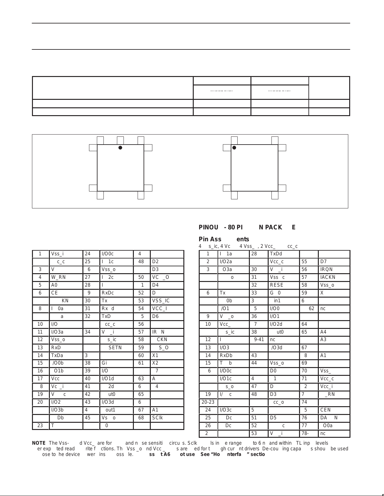
PIN CONFIGURATIONS
9
10
161
60
80
1
61
60
DWG #
68-Pin PLCC
TOP VIEW
26
27 43
44
80-Pin LQFP
TOP VIEW
20
21 40
41
SD00544
Figure 1. Pin Configurations
PINOUT - 68 PIN PACKAGE
Pin Assignments
4 Vss_ic, 4 Vcc_i, 4 Vss_o, 2 Vcc_o, 2Vcc_c
1
10
12
13
14
15
16
17
18
19
20
21
22
23
Vss_ic
2
Vcc_c
3
Vcc_i
4
W_RN
5
A0
6
CEN
7
DACKN
8
I/O0a
9
I/O1a
I/O2a
11
I/O3a
Vss_o
RxDa
TxDa
I/O0b
I/O1b
Vcc_o
Vcc_i
Vss_ic
I/O2b
I/O3b
RxDb
TxDb
24
25
26
27
28
29
30
31
32
33
34
35
36
37
38
39
40
41
42
43
44
45
46
I/O0c
I/O1c
Vss_o
I/O2c
I/O3c
RxDc
TxDc
RxDd
TxDd
Vcc_c
Vcc_i
Vss_ic
RESETN
Gin0
Gin1
I/O0d
I/O1d
I/O2d
Gout0
I/O3d
Gout1
Vss_o
D0
47
48
49
50
51
52
53
54
55
56
57
58
59
60
61
62
63
64
65
66
67
68
D1
D2
D3
VCC_O
D4
D5
VSS_IC
VCC_I
D6
D7
IRQN
IACKN
VSS_O
X1
X2
A7
A5
A4
A3
A2
A1
SClk
PINOUT - 80 PIN THIN PACKAGE
Pin Assignments
4 Vss_ic, 4 Vcc_i, 4 Vss_o, 2 Vcc_o, 2Vcc_c
1
2
3
4
5
6
7
8
9
10
11
12
13
14
15
16
17
18
19
20-23
24
25
26
27
I/O1a
I/O2a
I/O3a
Vss_o
RxDa
TxDa
I/O0b
I/O1b
Vcc_o
Vcc_i
Vss_ic
I/O2b
I/O3b
RxDb
TxDb
I/O0c
I/O1c
Vss_o
I/O2c
nc
I/O3c
RxDc
TxDc
RxDd
28
29
30
31
32
33
34
35
36
37
38
39-41
42
43
44
45
46
47
48
49
50
51
52
53
TxDd
Vcc_c
Vcc_i
Vss_ic
RESETN
Gin0
Gin1
I/O0d
I/O1d
I/O2d
Gout0
nc
I/O3d
Gout1
Vss_o
D0
D1
D2
D3
Vcc_o
D4
D5
Vss_ic
Vcc_i
54
55
56
57
58
59
60
61-62
63
64
65
66
67
68
69
70
71
72
73
74
75
76
77
78-80
D6
D7
IRQN
IACKN
Vss_o
X1
X2
nc
A7
A5
A4
A3
A2
A1
SClk
Vss_ic
Vcc_c
Vcc_i
W_RN
A0
CEN
DACKN
I/O0a
nc
NOTE: The Vss-ic and Vcc_i are for input and noise sensitive circuits. Sclk signals in the range of 3 to 6 ns and within TTL input levels may
alter expected read or write functions. The Vss _o and Vcc _o pins are used for the high current drivers. De-coupling capacitors should be used
as close to the device power pins as possible. Address bit A6 is not used. See “Host Interface” section.
1998 Sep 21
3
Page 4
Philips Semiconductors Preliminary specification
ÁÁÁ
ÁÁÁ
Á
Á
ÁÁÁ
ÁÁÁ
ÁÁÁ
ÁÁÁ
Á
Á
ÁÁÁ
ÁÁÁ
Á
Á
ÁÁÁ
ÁÁÁ
ÁÁÁ
ÁÁÁ
ÁÁÁ
ÁÁÁ
ÁÁÁ
ÁÁÁ
ÁÁÁ
ÁÁÁ
ÁÁÁ
Á
Á
ÁÁÁ
SC28L194Quad UART for 3.3V and 5V supply voltage
Pin Description
MNEMONIC
SClk
ÁÁÁÁ
CEN
A(7:0)
D(7:0)
W_RN
ÁÁÁÁ
DACKN
IRQN
ÁÁÁÁ
IACKN
TD(a-d)
RD(a-d)
I/O0(a-d)
I/O1(a-d)
I/O2(a-d)
I/O3(a-d)
Gin(1:0)
Gout(1:0)
RESETN
X1/CCLK
X2
ÁÁÁÁ
Power Supplies
NOTE:
1. Many output pins will have very fast edges, especially when lightly loaded (less than 20 pf). These edges may move as fast as 1 to 3 ns fall
or rise time. The user must be aware of the possible generation of ringing and reflections on improperly terminated interconnections. See
previous note on Sclk noise under pin assignments.
TYPE
I
ÁÁ
I
I
I/O
I
ÁÁ
O
O
ÁÁ
I
O
I
I/O
I/O
I/O
I/O
I
O
I
I
O
ÁÁ
I
DESCRIPTION
Host system clock. Used to time operations in the Host Interface and clock internal logic. Must be greater than
twice the frequency of highest X1, Counter/Timer, TxC (1x) or RxC (1x) input frequency.
БББББББББББББББББББББББББ
Chip select: Active low. When asserted, allows I/O access to QUART registers by host CPU. W_RN signal
indicates direction. (Must not be active in IACKN cycle)
Address lines (A[6] is NOT used. See “Host Interface” )
8-bit bi-directional data bus. Carries command and status information between 28L194 and the host CPU.
Used to convey parallel data for serial I/O between the host CPU and the 28L194
Write Read not control: When high indicates that the host CPU will write to a 28L194 register or transmit FIFO.
БББББББББББББББББББББББББ
When low, indicates a read cycle. 0 = Read; 1 = W rite
Data Acknowledge: Active low. When asserted, it signals that the last transfer of the D lines is complete.
Open drain requires a pull-up device.
Interrupt Request: Active low. When asserted, indicates that the 28L194 requires service for pending
interrupt(s). Open drain requires a pull-up device.
БББББББББББББББББББББББББ
Interrupt Acknowledge: Active low. When asserted, indicates that the host CPU has initiated an interrupt
acknowledge cycle. (Do not use CEN in an IACKN cycle)
Transmit Data: Serial outputs from the 4 UARTs.
Receive Data: Serial inputs to the 4 UARTs
Input/Output 0: Multi-use input or output pin for the UART.
Input/Output 1: Multi-use input or output pin for the UART.
Input/Output 2: Multi-use input or output pin for the UART.
Input/Output 3: Multi-use input or output pin for the UART.
Global general purpose inputs, available to any/all channels.
Global general purpose outputs, available from any channel.
Master reset: Active Low. Must be asserted at power up and may be asserted at other times to reset and
restart the system. See “Reset Conditions” at end of register map. Minimum width 10 SCLK.
Crystal 1 or Communication Clock: This pin may be connected to one side of a 2-8 MHz crystal. It may
alternatively be driven by an external clock in this frequency range. Standard frequency = 3.6864 MHz
Crystal 2: If a crystal is used, this is the connection to the second terminal. If a clock signal drives X1, this pin
БББББББББББББББББББББББББ
must be left unconnected.
16 pins total 8 pins for Vss, 8 pins for Vcc
ABSOLUTE MAXIMUM RATINGS
SYMBOL
T
T
V
V
PD
PD
amb
stg
CC
SS
Operating ambient temperature range
Storage temperature range
Voltage from VDD to V
Voltage from any pin to V
Package Power Dissipation (PLCC)
Package Power Dissipation (LQFP)
Derating factor above 25°C (PLCC package)
Derating factor above 25°C (LQFP package)
1
PARAMETER
4
SS
SS
RATING
2
See Note 3
-65 to +150
-0.5 to +7.0
-0.5 to VCC + 0.5
2.87
2
23
16
UNIT
°C
°C
V
V
W
W
mW/°C
mW/°C
NOTES:
1. Stresses above those listed under Absolute Maximum Ratings may cause permanent damage to the device. This is a stress rating only and
the functional operation of the device at these or any other conditions above those indicated in the Operation Section of this specification is
not implied.
2. For operating at elevated temperatures, the device must be derated based on +150°C maximum junction temperature.
3. Parameters are valid over specified temperature range. See Ordering Information table for applicable temperature range and operating
supply range.
4. This product includes circuitry specifically designed for the protewction of its internal devices from damaging effects of excessive static
charge.
1998 Sep 21
4
Page 5
Philips Semiconductors Preliminary specification
SC28L194Quad UART for 3.3V and 5V supply voltage
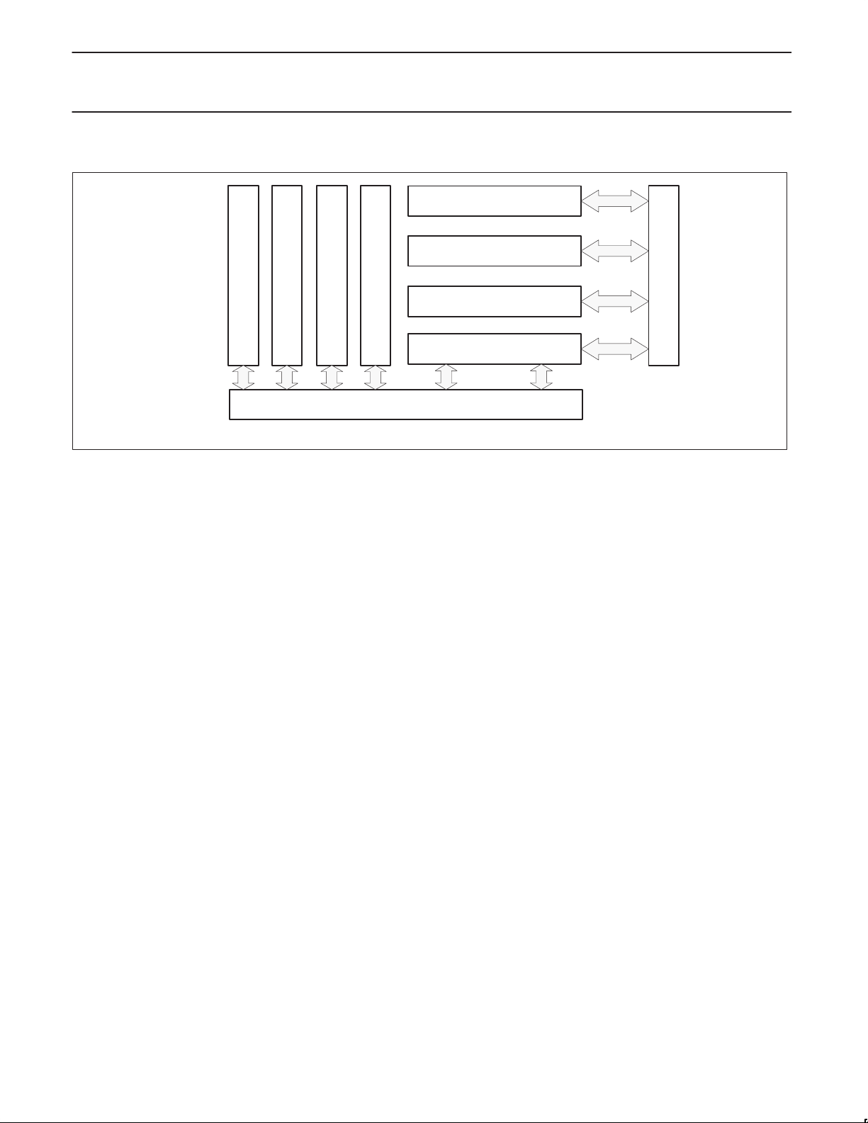
BLOCK DIAGRAM
FULL DUPLEX UART CHANNEL
FULL DUPLEX UART CHANNEL
HOST INTERFACE
As shown in the block diagram, the Quad UART consists of an
interrupt arbiter, host interface, timing blocks and four UART channel
blocks. The four channels blocks operate independently, interacting
only with the timing, host I/F and interrupt blocks.
GENERATOR
TIMING AND BAUD RATE
INTERRUPT ARBITRATION
INPUT BUFFERS AND OUTPUT DRIVERS
INTERFACE
I/O PORT TIMING AND
Block Diagram SC28L194
Figure 2. Block Diagram
FUNCTIONAL DESCRIPTION
The SC28L194 is composed of several functional blocks:
• Synchronous host interface block
• A timing block consisting of a common baud rate generator
making 22 industry standard baud rates and 2 16-bit counters
used for non-standard baud rate generation
• 4 identical independent full duplex UART channel blocks
• Interrupt arbitration system evaluating 24 contenders
• I/O port control section and change of state detectors.
CONCEPTUAL OVERVIEW
Host Interface
The Host interface is comprised of the signal pins CEN, W/RN,
IACKN, DACKN, IRQN Sclk and provides all the control for data
transfer between the external and internal data buses of the host
and the QUART. The host interface operates in a synchronous mode
with the system (Sclk) which has been designed for a nominal
operating frequency of 33 MHz. The interface operates in either of
two modes; synchronous or asynchronous to the Sclk However
the bus cycle within the QUART always takes place in four Sclk
cycles after CEN is recognized. These four cycles are the C1, C2,
C3, C4 periods shown in the timing diagrams. DACKN always
occurs in the C4 time and occurs approximately 18 ns after the
rising edge of C4.
Addressing of the various functions of the QUART is through the
address bus A(7:0). T o maintain upward compatibility with the
SC28L/C198 Octart the 8 bit address is still defined as such.
However A(6) is NOT used and is internally connected to Vss
(ground). The pin is, therefore, not included in the pin diagram. The
address space is controlled by A(5:0) and A(7). A[7], in a general
sense, is used to separate the data portion of the circuit from the
control portion.
FULL DUPLEX UART CHANNEL
FULL DUPLEX UART CHANNEL
Asynchronous bus cycle
The asynchronous mode requires one bus cycle of the chip select
(CEN) for each read or write to the chip. No more action will occur
on the bus after the C4 time until CEN is returned high.
Synchronous bus cycle
In the synchronous mode a read or write will be done every four
cycles of the Sclk. CEN does not require cycling but must remain
low to keep the synchronous accesses active. This provides a burst
mode of access to the chip.
In both cases each read or write operation(s) will be completed in
four (4) Sclk cycles. The difference in the two modes is only that the
asynchronous mode will not begin another bus cycle if the CEN
remains active after the four internal Sclk have completed. Internally
the asynchronous cycle will terminate after the four periods of Sclk
regardless of how long CEN is held active
In all cases the internal action will terminate at the withdrawal of
CEN. Synchronous CEN cycles shorter than multiples of four Sclk
cycles minus 1 Sclk and asynchronous CEN cycles shorter than four
Sclk cycles may cause short read or write cycles and produce
corrupted data transfers.
DATA DRIVERS AND MODEM INTERFACE
SD00524
Timing Circuits
The timing block consists of a crystal oscillator, a fixed baud rate
generator (BRG), a pair of programmable 16 bit register based
counters. A buffer for the System Clock generates internal timing for
processes not directly concerned with serial data flow.
Crystal Oscillator
The crystal oscillator operates directly from a crystal, tuned between
1.0 and 8.0 MHz, connected across the X1/CCLK and X2 inputs with
a minimum of external components. BRG values listed for the clock
select registers correspond to a 3.6864 MHz crystal frequency. Use
of a 7.3728 MHz crystal will double the Communication Clock
frequencies.
An external clock in the 100 KHz to 10 MHz frequency range may
be connected to X1/CCLK. If an external clock is used instead of a
crystal, X1/CCLK must be driven and X2 left floating. The X1 clock
serves as the basic timing reference for the baud rate generator
(BRG) and is available to the BRG timers. The X1 oscillator input
1998 Sep 21
5
Page 6

Philips Semiconductors Preliminary specification
SC28L194Quad UART for 3.3V and 5V supply voltage
may be left unused if the internal BRG is not used and the X1 signal
is not selected for any counter input.
Sclk - System Clock
A clock frequency, within the limits specified in the electrical
specifications, must be supplied for the system clock Sclk. To
ensure the proper operation of internal controllers, the Sclk
frequency provided, must be strictly greater than twice the frequency
of X1 crystal clock, or any external 1x data clock input. The system
clock serves as the basic timing reference for the host interface and
other internal circuits.
Baud Rate Generator BRG
The baud rate generator operates from the oscillator or external
X1/CCLK clock input and is capable of generating 22 commonly
used data communications baud rates ranging from 50 to 230.4K
baud. These common rates may be doubled (up to 460.8 and 500K
baud) when faster clocks are used on the X1/X2 clock inputs. (See
Receiver and Transmitter Clock Select Register descriptions.) All of
these are available simultaneously for use by any receiver or
transmitter. The clock outputs from the BRG are at 16X the actual
baud rate.
BRG Counters (Used for random baud rate generation)
The two BRG Timers are programmable 16 bit dividers that are used
for generating miscellaneous clocks. These clocks may be used by
any or all of the receivers and transmitters in the Octart or output on
the general purpose output pin GPO.
Each timer unit has eight different clock sources available to it as
described in the BRG Timer Control Register. (BRGTCR). Note that
the timer run and stop controls are also contained in this register.
The BRG Timers generate a symmetrical square wave whose half
period is equal in time to the division of the selected BRG Timer
clock source by the number loaded to the BRG Timer Reload
Registers ( BRGTRU and BRGTRL). Thus, the output frequency will
be the clock source frequency divided by twice the value loaded to
the BRGTRU and BRGTRL registers. This is the result of counting
down once for the high portion of the output wave and once for the
low portion.
Whenever the these timers are selected via the receiver or
transmitter Clock Select register their output will be configured as a
16x clock for the respective receiver or transmitter. Therefore one
needs to program the timers to generate a clock 16 times faster than
the data rate. The formula for calculating ’n’, the number loaded to
the BRGTRU and BRGTRL registers, is shown below.
BRG Timer Input frequency
n
2 16 desired baud rate
Note: ’n’ may assume values of 0 and 1. In previous Philips data
communications controllers these values were not allowed.
The BRG timer input frequency is controlled by the BRG Timer
control register (BRGTCR)
The frequency generated from the above formula will be at a rate 16
times faster than the desired baud rate. The transmitter and receiver
state machines include divide by 16 circuits which provide the final
frequency and provide various timing edges used in the qualifying
the serial data bit stream. Often this division will result in a
non-integer value; 26.3 for example. One may only program integer
numbers to a digital divider. There for 26 would be chosen. If 26.7
–1
was the result of the division then 27 would be chosen. This gives a
baud rate error of 0.3/26.3 or 0.3/26.7. which yields a percentage
error of 1.14% or 1.12% respectively; well within the ability of the
asynchronous mode of operation.
One should be cautious about the assumed benign effects of small
errors since the other receiver or transmitter with which one is
communicating may also have a small error in the precise baud rate.
In a “clean” communications environment using one start bit, eight
data bits and one stop bit the total difference allowed between the
transmitter and receiver frequency is approximately 4.6%. Less than
eight data bits will increase this percentage.
Channel Blocks
There are four channel blocks, each containing an I/O port control, a
data format control, and a single full duplex UART channel
consisting of a receiver and a transmitter with their associated 16
byte FIFOs. Each block has its own status register, interrupt status
and interrupt mask registers and their interface to the interrupt
arbitration system.
A highly programmable character recognition system is also
included in each block. This system is used for the Xon/Xoff flow
control and the multi-drop (”9 bit mode”) address character
recognition. It may also be used for general purpose character
recognition.
Four I/O pins are provided for each channel. These pins are
configured individually to be inputs or outputs. As inputs they may
be used to bring external data to the bus, as clocks for internal
functions or external control signals. Each I/O pin has a “Change of
State” detector. The change detectors are used to signal a change in
the signal level at the pin (Either 0 to 1 or 1 to 0) The level change
on these pins must be stable for 25 to 50 Us (two edges of the 38.4
KHz baud rate clock) before the detectors will signal a valid change.
These are typically used for interface signals from modems to the
QUART and from there to the host. See the description of the
“UART channel” under detailed descriptions below.
Character Recognition
Character recognition is specific to each of the four UARTs. Three
programmable characters are provided for the character recognition
for each channel. The three are general purpose in nature and may
be set to only cause an interrupt or to initiate some rather complex
operations specific to “Multi-drop” address recognition or in-band
Xon/Xoff flow control.
Character recognition is accomplished via CAM memory. The
Content Addressable Memory continually examines the incoming
data stream. Upon the recognition of a control character appropriate
bits are set in the Xon/Xoff Interrupt Status Register (XISR) and
Interrupt Status Register (ISR). The setting of these bit(s) will initiate
any of the automatic sequences or and/or an interrupt that may have
enabled via the MR0 register.
The characters of the recognition system are not controlled by the
software or hardware reset. They do not have a pre-defined “reset
value”. They may, however, be loaded by a “Gang White” or “Gang
Load” command as described in the “Xon Xoff Characters”
paragraph.
Note: Character recognition is further described in the
of Operation.
Minor Modes
1998 Sep 21
6
Page 7

Philips Semiconductors Preliminary specification
SC28L194Quad UART for 3.3V and 5V supply voltage
Interrupt Control
The interrupt system determines when an interrupt should be
asserted thorough an arbitration (or bidding) system. This arbitration
is exercised over the several systems within the QUART that may
generate an interrupt. These will be referred to as “interrupt
sources”. There are 64 in all. In general the arbitration is based on
the fill level of the receiver FIFO or the empty level of the transmitter
FIFO. The FIFO levels are encoded into a four bit number which is
concatenated to the channel number and source identification code.
All of this is compared (via the bidding or arbitration process) to a
user defined “threshold”. When ever a source exceeds the
numerical value of the threshold the interrupt will be generated.
At the time of interrupt acknowledge (IACKN) the source which has
the highest bid (not necessarily the source that caused the interrupt
to be generated) will be captured in a “Current Interrupt Register”
(CIR). This register will contain the complete definition of the
interrupting source: channel, type of interrupt (receiver, transmitter,
change of state, etc.), and FIFO fill level. The value of the bits in the
CIR are used to drive the interrupt vector and global registers such
that controlling processor may be steered directly to the proper
service routine. A single read operation to the CIR provides all the
information needed to qualify and quantify the most common
interrupt sources.
The interrupt sources for each channel are listed below.
• Transmit FIFO empty level for each channel
• Receive FIFO Fill level for each channel
• Change in break received status for each channel
• Receiver with error for each channel
• Change of state on channel input pins
• Receiver Watch-dog Time out Event
• Xon/Xoff character recognition
• Address character recognition
Associated with the interrupt system are the interrupt mask register
(IMR) and the interrupt status register (ISR) resident in each UART.
Programming of the IMR selects which of the above sources may
enter the arbitration process. Only the bidders in the ISR whose
associated bit in the IMR is set to one (1) will be permitted to enter
the arbitration process. The ISR can be read by the host CPU to
determine all currently active interrupting conditions. For
convenience the bits of the ISR may be masked by the bits of the
IMR. Whether the ISR is read unmasked or masked is controlled by
the setting of bit 6 in MR1.
Global Registers
The “Global Registers”, 19 in all, are driven by the interrupt system.
These are not real hardware devices. They are defined by the
content of the CIR (Current Interrupt Register) as a result of an
interrupt arbitration. In other words they are indirect registers
contained in the Current Interrupt Register (CIR) which the CIR uses
to point to the source and context of the QUART sub circuit
presently causing an interrupt. The principle purpose of these
“registers” is improving the efficiency of the interrupt service.
The global registers and the CIR update procedure are further
described in the
I/O Ports
Each of the four UART blocks contains an I/O section of four ports.
These ports function as a general purpose post section which
services the particular UART they are associated with. External
clocks are input and internal clocks are output through these ports.
Interrupt Arbitration
system
Each of the four pins has a change of state detector which will signal
a change (0 to 1 or 1 to 0) at the pin. The change of state detectors
are individually enabled and may be set to cause and interrupt.
These pins will normally be used for flow control hand-shaking and
the interface to a modem. Their control is further described in
section and the I/OPCR register.
Ports
I/O
DET AILED DESCRIPTIONS
RECEIVER AND TRANSMITTER
The Quad UART has four full duplex asynchronous
receiver/transmitters. The operating frequency for the receiver and
transmitter can be selected independently from the baud rate
generator, the counter , or from an external input. Registers that are
central to basic full-duplex operation are the mode registers (MR0,
MR1 and MR2), the clock select registers (RxCSR and TxCSR), the
command register (CR), the status register (SR), the transmit
holding register (TxFIFO), and the receive holding register
(RxFIFO).
Transmitter
The transmitter accepts parallel data from the CPU and converts it
to a serial bit stream on the TxD output pin. It automatically sends a
start bit followed by the programmed number of data bits, an
optional parity bit, and the programmed number of stop bits. The
least significant bit is sent first. Each character is always “framed” by
a single start bit and a stop bit that is 9/16 bit time or longer. If a new
character is not available in the TxFIFO, the TxD output remains
high, the “marking” position, and the TxEMT bit in the SR is set to 1.
Transmitter Status Bits
The SR (Status Register, one per UART) contains two bits that show
the condition of the transmitter FIFO. These bits are TxRDY and
TxEMT. TxRDY means the TxFIFO has space available for one or
more bytes; TxEMT means The TxFIFO is completely empty and
the last stop bit has been completed. TxEMT can not be active
without TxRDY also being active. These two bits will go active upon
initial enabling of the transmitter . They will extinguish on the disable
or reset of the transmitter.
Transmission resumes and the TxEMT bit is cleared when the CPU
loads at least one new character into the TxFIFO. The TxRDY will
not extinguish until the TxFIFO is completely full. The TxRDY bit will
always be active when the transmitter is enabled and there is at
lease one open position in the TxFIFO.
The transmitter is disabled by reset or by a bit in the command
register (CR). The transmitter must be explicitly enabled via the CR
before transmission can begin. Note that characters cannot be
loaded into the TxFIFO while the transmitter is disabled, hence it is
necessary to enable the transmitter and then load the TxFIFO. It is
not possible to load the TxFIFO and then enable the transmission.
Note the difference between transmitter disable and transmitter
reset. The reset is affected by either software or hardware. When
reset, the transmitter stops transmission immediately. The transmit
data output will be driven high, transmitter status bits set to zero and
any data remaining in the TxFIFO will be discarded.
The transmitter disable is controlled by the Tx Enable bit in the
command register. Setting this bit to zero will not stop the transmitter
immediately, but will allow it to complete any tasks presently
underway. It is only when the last character in the TxFIFO and its
stop bit(s) have been transmitted that the transmitter will go to its
disabled state. While the transmitter enable/disable bit in the
command register is at zero, the TxFIFO will not accept any
additional characters.
1998 Sep 21
7
Page 8

Philips Semiconductors Preliminary specification
SC28L194Quad UART for 3.3V and 5V supply voltage
Transmission of “Break”
Transmission of a break character is often needed as a
synchronizing condition in a data stream. The “break” is defined as a
start bit followed by all zero data bits by a zero parity bit (if parity is
enabled) and a zero in the stop bit position. The forgoing is the
minimum time to define a break. The transmitter can be forced to
send a break (continuous low condition) by issuing a start break
command via the CR. This command does not have any timing
associated with it. Once issued the TxD output will be driven low
(the spacing condition) and remain there until the host issues a
command to “stop break” via the CR or the transmitter is issued a
software or hardware reset. In normal operation the break is usually
much longer than one character time.
1x and 16x modes, Transmitter
The transmitter clocking has two modes: 16x and 1x. Data is always
sent at the 1x rate. However the logic of the transmitter may be
operated with a clock that is 16 times faster than the data rate or at
the same rate as the data i.e. 1x. All clocks selected internally for
the transmitter (and the receiver) will be 16x clocks. Only when an
external clock is selected may the transmitter logic and state
machine operate in the 1x mode. The 1x or 16x clocking makes little
difference in transmitter operation. (this is not true in the receiver) In
the 16X clock mode the transmitter will recognize a byte in the
TxFIFO within 1/16 to 2/16 bit time and thus begin transmission of
the start bit; in the 1x mode this delay may be up to 2 bit times.
Transmitter FIFO
The transmitter buffer memory is a 16 byte by 8 bit ripple FIFO. The
host writes characters to this buffer. This buffer accepts data only
when the transmitter is enabled. The transmitter state machine
reads them out in the order they were received and presents them to
the transmitter shift register for serialization. The transmitter adds
the required start, parity and stop bits as required the MR2 register
programming. The start bit (always one bit time in length) is sent first
followed by the least significant bit (LSB) to the most significant bit
(MSB) of the character, the parity bit (if used) and the required stop
bit(s).
Logic associated with the FIFO encodes the number of empty
positions available in a four bit value.. This value is concatenated
with the channel number and type interrupt type identifier and
presented to the interrupt arbitration system. The encoding of the
“positions empty” value is always 1 less than the number of
available positions. Thus, an empty TxFIFO will bid with the value or
15; when full it will not bid at all; one position empty bids with the
value 0. A full FIFO will not bid since a character written to it will be
lost
Normally a TxFIFO will present a bid to the arbitration system when
ever it has one or more empty positions. The MR0[5:4] allow the
user to modify this characteristic so that bidding will not start until
one of four levels (empty, 3/4 empty, 1/2 empty, not full) have been
reached. As will be shown later this feature may be used to make
slight improvements in the interrupt service efficiency. A similar
system exists in the receiver.
Receiver
The receiver accepts serial data on the RxD pin, converts the serial
input to parallel format, checks for start bit, stop bit, parity bit (if
any),framing error or break condition, and presents the assembled
character and its status condition to the CPU via the RxFIFO. Three
status bits are FIFOed with each character received. The RxFIFO is
really 11 bits wide; eight data and 3 status. Unused FIFO bits for
character lengths less than 8 bits are set to zero. It is important to
note that receiver logic considers the entire message to be
contained within the start bit to the stop bit. It is not aware that a
message may contain many characters. The receiver returns to its
idle mode at the end of each stop bit! As described below it
immediately begins to search for another start bit which is normally,
of course, immediately forth coming.
1x and 16x Mode, Receiver
The receiver operates in one of two modes; 1x and 16x. Of the two,
the 16x is more robust and the preferred mode. Although the 1x
mode may allow a faster data rate is does not provide for the
alignment of the receiver 1x data clock to that of the transmitter. This
strongly implies that the 1x clock of the remote transmitter is
available to the receiver; the two devices are physically close to
each other.
The 16x mode operates the receiver logic at a rate 16 times faster
than the 1x data rate. This allows for validation of the start bit,
validation of level changes at the receiver serial data input (RxD),
and a stop bit length as short as 9/16 bit time. Of most importance in
the 16x mode is the ability of the receiver logic to align the phase of
the receiver 1x data clock to that of the transmitter with an accuracy
of less than 1/16 bit time.
When the receiver is enabled ( via the CR register) it begins looking
for a high to low (mark to space) transition on the RxD input pin. If a
transition is detected, an internal counter running at 16 times the
data rate is reset to zero. If the RxD remains low and is still low
when the counter reaches a count of 7 the receiver will consider this
a valid start bit and begin assembling the character. If the RxD input
returns to a high state the receiver will reject the previous high to low
(mark to space) transition on the RxD input pin. This action is the
“validation” of the start bit and also establishes the phase of the
receiver 1x clock to that of the transmitter The counter operating at
16x the data rate is the generator for the 1x data rate clock. With the
phase of the receiver 1x clock aligned to the falling of the start bit
(and thus aligned to the transmitter clock) AND with a valid start bit
having been verified the receiver will continue receiving bits by
sampling the RxD input on the rising edge of the 1x clock that is
being generated by the above mentioned counter running 16 times
the data rate. Since the falling edge of the 1x clock was aligned to
falling edge of the start bit then the rising of the clock will be in the
“center” of the bit cell.
This action will continue until a full character has been assembled.
Parity, framing, and stop bit , and break status is then assembled
and the character and its status bits are loaded to the RxFIFO At
this point the receiver has finished its task for that character and will
immediately begin the search for another start bit.
Receiver Status Bits
There are five (5) status bits that are evaluated with each byte (or
character) received: received break, framing error, parity error,
overrun error, and change of break. The first three are appended to
each byte and stored in the RxFIFO. The last two are not
necessarily related to the a byte being received or a byte that is in
the RxFIFO. They are however developed by the receiver state
machine.
The “received break” will always be associated with a zero byte in
the RxFIFO. It means that zero character was a break character and
not a zero data byte. The reception of a break condition will always
set the “change of break” (see below) status bit in the Interrupt
Status Register(ISR).
A framing error occurs when a non zero character was seen and
that character has a zero in the stop bit position.
1998 Sep 21
8
Page 9

Philips Semiconductors Preliminary specification
SC28L194Quad UART for 3.3V and 5V supply voltage
The parity error indicates that the receiver generated parity was not
the same as that sent by the transmitter.
The overrun error occurs when the RxFIFO is full, the receiver shift
register is full and another start bit is detected. At this moment the
receiver has 17 valid characters and the start bit of the 18th has
been seen. At this point the host has approximately 7/16 bit time to
read a byte from the RxFIFO or the overrun condition will be set and
the 18th character will overrun the 17th and the 19th the 18th and so
on until an open position in the RxFIFO is seen. The meaning of the
overrun is that data has been lost. Data in the RxFIFO remains
valid. The receiver will begin placing characters in the RxFIFO as
soon as a position becomes vacant.
Note: Precaution must be taken when reading an overrun FIFO.
There will be 16 valid characters. Data will begin loading as soon as
the first character is read. The 17
received as valid but it will not be known how many characters were
lost between the two characters of the 16
th.
character will have been
th.
and 17
th.
reads of the
RxFIFO
The “Change of break” means that either a break has been detected
or that the break condition has been cleared. This bit is available in
the ISR. The beginning of a break will be signaled by the break
change bit being set in the ISR AND the received break bit being set
in the SR. At the termination of the break condition only the change
of break in the ISR will be set. After the break condition is detected
the termination of the break will only be recognized when the RxD
input has returned to the high state for two successive edges of the
1x clock; 1/2 to 1 bit time.
The receiver is disabled by reset or via CR commands. A disabled
receiver will not interrupt the host CPU under any circumstance in
the normal mode of operation. If the receiver is in the multi-drop or
special mode, it will be partially enabled and thus may cause an
interrupt. Refer to section on Wake-Up and minor modes and the
register description for MR1 for more information.
Receiver FIFO
The receiver buffer memory is a 16 byte ripple FIFO with three
status bits appended to each data byte. (The FIFO is then 16 11 bit
“words”). The receiver state machine gathers the bits from the
receiver shift register and the status bits from the receiver logic and
writes the assembled byte and status bits to the RxFIFO. Logic
associated with the FIFO encodes the number of filled positions for
presentation to the interrupt arbitration system. The encoding is
always 1 less than the number of filled positions. Thus, a full
RxFIFO will bid with the value or 15; when empty it will not bit at all;
one position occupied bids with the value 0. An empty FIFO will not
bid since no character is available. Normally RxFIFO will present a
bid to the arbitration system when ever it has one or more filled
positions. The MR2[3:2 bits allow the user to modify this
characteristic so that bidding will not start until one of four levels
(one or more filled, 1/2 filled, 3/4 filled, full) have been reached. As
will be shown later this feature may be used to make slight
improvements in the interrupt service efficiency . A similar system
exists in the transmitter.
RxFIFO Status: Status Reporting Modes
The description below applies to the upper three bits in the “Status
Register” These three bits are not “in the status register”; They are
part of the RxFIFO. The three status bits at the top of the RxFIFO
are presented as the upper three bits of the status register included
in each UART.
The error status of a character , as reported by a read of the SR
(status register upper three bits) can be provided in two ways, as
programmed by the error mode control bit in the mode register:
“Character mode” or the “Block Mode”. The block mode may be
further modified (via a CR command) to set the status bits as the
characters enter the FIFO or as they are read from the FIFO.
In the ’character’ mode, status is provided on a character by
character basis as the characters are read from the RxFIFO: the
“status” applies only to the character at the top of the RxFIFO - The
next character to be read.
In the ’block’ mode, the status provided in the SR for these three bits
is the logical OR of the status for all characters coming to the top of
the RxFIFO, since the last reset error command was issued. In this
mode each of the status bits stored in the RxFIFO are passed
through a latch as they are sequentially read. If any of the
characters has an error bit set then that latch will set and remain set
until reset with an “Reset Error” command from the command
register or a receiver reset. The purpose of this mode is indicating
an error in the data block as opposed to an error in a character
The latch used in the block mode to indicate “problem data” is
usually set as the characters are read out of the RxFIFO. Via a
command in the CR the latch may be configured to set the latch as
the characters are pushed (loaded to) the RxFIFO. This gives the
advantage of indicating “problem data” 16 characters earlier.
In either mode, reading the SR does not affect the RxFIFO. The
RxFIFO is ’popped’ only when the RxFIFO is read. Therefore, the
SR should be read prior to reading the corresponding data
character.
If the RxFIFO is full when a new character is received, that
character is held in the receive shift register until a RxFIFO position
is available. At this time there are 17 valid characters in the RxFIFO.
If an additional character is received while this state exists, the
contents of the RxFIFO are not affected: the character previously in
the shift register is lost and the overrun error status bit, SR[4], will be
set upon receipt of the start bit of the new (overrunning) character.
I/O Ports
Each of the four UARTs includes four I/O ports equipped with
“change of state” detectors. The pins are individually programmable
for an input only function or one of three output functions. These
functions are controlled by the “I/O Port Configuration Register
(I/OPCR)) They will normally be used for the RTSN-CTSN, DTR
hardware signals, RxD or TxD input or output clocks or switch inputs
as well as data out put from the I/OPIOR register.
It is important to note that the input circuits are always active. That is
the signal on a port, whether it is derived from an internal or external
source is always available to the internal circuits associated with an
input on that port.
The “Change of State” (COS) detectors are sensitive to both a 1 to 0
or a 0 to 1 transition. The detectors are controlled by the internal
38.4 KHz baud rate and will signal a change when a transition has
been stable for two rising edges of this clock. Thus a level on the I/O
ports must be stable for 26 s to 52 s. Defining a port as an output
will disable the COS detector at that port. The condition of the four
I/O pins and their COS detectors is available at any time in the IPR
(Input Port Register)
The control of data and COS enable for these ports is through the
I/OPIOR register. This is a read/write register and gives individual
control to the enabling of the change of state detectors and also to
the level driven by I/O pins when programmed to drive the logic level
written to the four lower bits of the I/OPIOR. A read of this register
will indicate the data on the pin at the time of the read and the state
of the enabled COS detectors.
1998 Sep 21
9
Page 10

Philips Semiconductors Preliminary specification
SC28L194Quad UART for 3.3V and 5V supply voltage
General Purpose Pins
In addition to the I/O ports for each UART four other ports are
provided which service the entire chip. Two are dedicated as inputs
and two are as outputs. The Gin1 and Gin0 are the input pins; Gout0
and Gout1 the outputs. These ports are multiplexed to nearly every
functional unit in the chip. See the registers which describe the
multitude of connections available for these pins. The Gout0 and
Gout1 pins are highly multiplexed outputs and are controlled by four
(4) registers: GPOSR, GPOR, GPOC and GPOD. The Gin0 and
Gin1 pins are available to the receivers and transmitters, BRG
counters and the Gout0 and Gout1 pins.
Global Registers
The “Global Registers”, 19 in all, are driven by the interrupt system.
These are not real hardware devices. They are defined by the
content of the CIR (Current Interrupt Register) as a result of an
interrupt arbitration. In other words they are indirect registers pointed
to by the content of the CIR. The list of global register follows:
GIBCR The byte count of the interrupting FIFO
GICR Channel number of the interrupting channel
GITR Type identification of interrupting channel
GRxFIFO Pointer to the interrupting receiver FIFO
GTxFIFO Pointer to the interrupting transmitter FIFO
A read of the GRxFIFO will give the content of the RxFIFO that
presently has the highest bid value. The purpose of this system is to
enhance the efficiency of the interrupt system. The global registers
and the CIR update procedure are further described in the
Arbitration
system
Interrupt
Character Recognition
The character recognition circuits are basically designed to provide
general purpose character recognition. Additional control logic has
been added to allow for Xon/Xoff flow control and for recognition of
the address character in the multi-drop or “wake-up” mode. This
logic also allows for the generation of an interrupts in either the
general purpose recognition mode or the specific conditions
mentioned above.
Xon Xoff Characters
The programming of these characters is usually done individually.
However a method has been provided to write to all of registers in
one operation. There are “Gang Load” and a “Gang Write”
commands provided in the channel A Command Register. When
these commands are executed all registers are programmed with
the same characters. The “write” command loads a used defined
character; the ’load” command loads the standard Xon/Xoff
characters. Xon is x’11; Xof f x’13’. Any enabling of the Xon/Xoff
functions will use the contents of the Xon and Xoff character
registers as the basis on which recognition is predicated.
Multi-drop or Wake-up or 9-bit Mode
This mode is used to address a particular UART among a group
connected to the same serial data source. Normally it is
accomplished by redefining the meaning of the parity bit such that it
indicates a character as address or data. While this method is fully
supported in the SC28L194 it also supports recognition of the
character itself. Upon recognition of its address the receiver will be
enabled and data pushed onto the RxFIFO.
Further the Address recognition has the ability, if so programmed, to
disable (not reset) the receiver when an address is seen that is not
recognized as its own. The particular features of “Auto Wake and
Auto Doze” are described in the detail descriptions below.
Note: Care should be taken in the programming of the character
recognition registers. Programming x’00, for example, may result in
a break condition being recognized as a control character. This will
be further complicated when binary data is being processed.
Character Stripping
The MR0 register provides for stripping the characters used for
character recognition. Recall that the character recognition may be
conditioned to control several aspects of the communication.
However this system is first a character recognition system. The
status of the various states of this system are reported in the XISR
and ISR registers. The character stripping of this system allows for
the removal of the specified control characters from the data stream:
two for the Xon /Xoff and one for the Wake-up. Via control in the
MR0 register these characters may be discarded (stripped) from the
data stream when the recognition system “sees” them or they may
be sent on the RxFIFO. Whether they are stripped or not the
recognition will process them according to the action requested: flow
control, Wake-up, interrupt generation, etc. Care should be
exercised in programming the stripping option if noisy environments
are encountered. If a normal character was corrupted to an Xoff
character turned off the transmitter and it was then stripped, then the
stripping action could make it difficult to determine the cause of
transmitter stopping.
Interrupt Arbitration and IRQN Generation
Interrupt arbitration is the process used to determine that an
interrupt request should be presented to the host. The arbitration is
carried out between the “Interrupt Threshold” and the “sources”
whose interrupt bidding is enabled by the IMR. The interrupt
threshold is part of the ICR (Interrupt Control Register) and is a
value programmed by the user. The “sources” present a value to the
interrupt arbiter. That value is derived from four fields: the channel
number, type of interrupt source, FIFO fill level, and programmable
value. Only when one or more of these values exceeds the
threshold value in the interrupt control register will the interrupt
request (IRQN) be asserted.
Following assertion of the IRQN the host will either assert
IACKN(Interrupt Acknowledge) or will use the command to “Update
the CIR”. At the time either action is taken the CIR will capture the
value of the source that is prevailing in the arbitration process. (Call
this value the winning bid)
The value in the CIR is the central quantity that results from the
arbitration. It contains the identity of the interrupting channel, the
type of interrupt in that channel (RxD, TxD, COS etc.) the fill levels
of the RxD or TxD FIFOs and , in the case of an RxD interrupt an
indicator of error data or good data. It also drives the Global
Registers associated with the interrupt. Most importantly it drives
the modification of the Interrupt Vector.
The arbitration process is driven by the Sclk. It scans the 10 bits of
the arbitration bus at the Sclk rate developing a value for the CIR
every 22 Sclk cycles. New arbitration values presented to the
arbitration block during an arbitration cycle will be evaluated in the
next arbitration cycle.
For sources other than receiver and transmitters the user may set
the high order bits of an interrupt source’s bid value, thus tailoring
the relative priority of the interrupt sources. The priority of the
receivers and transmitters is controlled by the fill level of their
respective FIFOs. The more filled spaces in the RxFIFO the higher
the bid value; the more empty spaces in the TxFIFO the higher its
priority. Channels whose programmable high order bits are set will
1998 Sep 21
10
Page 11

Philips Semiconductors Preliminary specification
SC28L194Quad UART for 3.3V and 5V supply voltage
be given interrupt priority higher than those with zeros in their high
order bits , thus allowing increased flexibility. The transmitter and
receiver bid values contain the character counts of the associated
FIFOs as high order bits in the bid value. Thus, as a receiver’s
RxFIFO fills, it bids with a progressively higher priority for interrupt
service. Similarly, as empty space in a transmitter’s TxFIFO
increases, its interrupt arbitration priority increases.
IACKN Cycle, Update CIR
When the host CPU responds to the interrupt, it will usually assert
the IACKN signal low. This will cause the QUART to generate an
IACKN cycle in which the condition of the interrupting device is
determined. When IACKN asserts, the last valid interrupt number is
captured in the CIR. The value captured presents most of the
important details of the highest priority interrupt at the moment the
IACKN (or the “Update CIR” command) was asserted.
The Quad UART will respond to the IACKN cycle with an interrupt
vector. The interrupt vector may be a fixed value, the content of the
Interrupt Vector Register, or ,when “Interrupt Vector Modification is
enabled via ICR, it may contain codes for the interrupt type and/or
interrupting channel. This allows the interrupt vector to steer the
interrupt service directly to the proper service routine. The interrupt
value captured in the CIR remains until another IACKN cycle occurs
or until an “Update CIR” command is given to the QUART. The
interrupting channel and interrupt type fields of the CIR set the
current “interrupt context” of the QUART. The channel component of
the interrupt context allows the use of Global Interrupt Information
registers that appear at fixed positions in the register address map.
For example, a read of the Global RxFIFO will read the channel B
RxFIFO if the CIR interrupt context is channel b receiver. At another
time read of the GRxFIFO may read the channel D RxFIFO (CIR
holds a channel D receiver interrupt) and so on. Global registers
exist to facilitate qualifying the interrupt parameters and for writing to
and reading from FIFOs without explicitly addressing them.
The CIR will load with x’00 if IACKN or Update CIR is asserted when
the arbitration circuit is NOT asserting an interrupt. In this condition
there is no arbitration value that exceeds the threshold value.
Polling
Many users prefer polled to interrupt driven service where there are
a large number of fast data channels and/or the host CPU’s other
interrupt overhead is low. The Quad UART is functional in this
environment.
The most efficient method of polling is the use of the “update CIR”
command (with the interrupt threshold set to zero) followed by a
read of the CIR. This dummy write cycle will perform the same CIR
capture function that an IACKN falling edge would accomplish in an
interrupt driven system. A subsequent read of the CIR, at the same
address, will give information about an interrupt, if any. If the CIR
contains 0s, no interrupt is awaiting service. If the value is non-zero,
the fields of the CIR may be decoded for type, channel and
character count information. Optionally , the global interrupt registers
may be read for particular information about the interrupt status or
use of the global RxD and TxD registers for data transfer as
appropriate. The interrupt context will remain in the CIR until another
update CIR command or an IACKN cycle is initiated by the host
CPU occurs. The CIR loads with x’00 if Update CIR is asserted
when the arbitration circuit has NOT detected arbitration value that
exceeds the threshold value.
Traditional methods of polling status registers may also be used.
They of course are less efficient but give the most variable and
quickest method of changing the order in which interrupt sources
are evaluated and interrogated.
Enabling and Activating Interrupt Sources
An interrupt source becomes enabled when its interrupt capability is
set by writing to the Interrupt Mask Register, IMR. An interrupt
source can never generate an IRQN or have its “bid” or interrupt
number appear in the CIR unless the source has been enabled by
the appropriate bit in an IMR.
An interrupt source is active if it is presenting its bid to the interrupt
arbiter for evaluation. Most sources have simple activation
requirements. The watch-dog timer, break received, Xon/Xoff or
Address Recognition and change of state interrupts become active
when the associated events occur and the arbitration value
generated thereby exceeds the threshold value programmed in the
ICR (Interrupt Control Register).
The transmitter and receiver functions have additional controls to
modify the condition upon which the initiation of interrupt “bidding”
begins: the TxINT and RxINT fields of the MR0 and MR2 registers.
These fields can be used to start bidding or arbitration when the
RxFIFO is not empty, 50% full, 75% full or 100% full. For the
transmitter it is not full, 50% empty, 75% empty and empty.
Example: To increase the probability of transferring the contents of a
nearly full RxFIFO, do not allow it to start bidding until 50% or 75%
full. This will prevent its relatively high priority from winning the
arbitration process at low fill levels. A high threshold level could
accomplish the same thing, but may also mask out low priority
interrupt sources that must be serviced. Note that for fast channels
and/or long interrupt latency times using this feature should be used
with caution since it reduces the time the host CPU has to respond
to the interrupt request before receiver overrun occurs.
Setting Interrupt Priorities
The bid or interrupt number presented to the interrupt arbiter is
composed of character counts, channel codes, fixed and
programmable bit fields. The interrupt values are generated for
various interrupt sources as shown in the table below: The value
represented by the bits 9 to 3 in the table below are compared
against the value represented by the “Threshold. The “Threshold”
,bits 6 to 0 of the ICR (Interrupt Control Register), is aligned such
that bit 6 of the threshold is compared to bit 9 of the interrupt value
generated by any of the sources. When ever the value of the
interrupt source is greater than the threshold the interrupt will be
generated.
The channel number arbitrates only against other channels. The
threshold is not used for the channel arbitration. This results in
channel D having the highest arbitration number. The decreasing
order is D-to-A. If all other parts of an arbitration are equal then the
channel number will determine which channel will dominate in the
arbitration process.
1998 Sep 21
11
Page 12
Philips Semiconductors Preliminary specification
SC28L194Quad UART for 3.3V and 5V supply voltage
Table 1. Interrupt Arbitration Priority
Type
Receiver w/o error
Receiver w/ error
Transmitter
Change of Break
Change of State
Xon/Xoff
Address Recognition
Receiver Watch-dog
Threshold
B9
RxFIFO Byte Count -1
RxFIFO Byte Count -1
0
Programmed Field
Programmed Field
Programmed Field
Programmed Field
RxFIFO Byte Count -1
Bits 6:0 of Interrupt Control Register
B8
TxFIFO Byte Count -1
B7
0
0
0
0
B6
0
1
0
1
1
0
As RxFIFO Above
B5
B4
0
0
0
1
1
1
1
B3
1
1
0
0
0
1
1
Channel No
Channel No
Channel No
Channel No
Channel No
Channel No
Channel No
Channel No
000
Bits 2:0
Note several characteristics of the above table in bits 6:3. These bits
contain the identification of the bidding source as indicated below:
x001 Receiver without error
x101 Receiver with error
xx00 Transmitter
0010 Change of Break
0110 Change of State on I/O Ports
0111 Xon/Xoff Event
0011 Address Recognition
The codes form bits 6:3 drive part of the interrupt vector modification
and the Global Interrupt Type Register. The codes are unique to
each source type and Identify them completely. The channel
numbering progresses from “a” to “d” as the binary numbers 000 to
011 and identify the interrupting channel uniquely. As the channels
arbitrate “d” will have the highest bidding value and “a” the lowest
Note that the transmitter byte count is off-set from that of the
receiver by one bit. This is to give the receiver more authority in the
arbitration since and over-run receiver corrupts the message but an
under-run transmitter is not harmful. This puts some constraints on
how the threshold value is selected. If a threshold is chosen that has
its MSB set to one then a transmitter can never generate an
interrupt! Of course the counter point to this is the desire to set the
interrupt threshold high so interrupts occur only when a maximum or
near maximum number of characters may be transferred.
To give some control over this dilemma control bits have been
provided in the MR0 and MR2 registers of each channel to
individually control when a receiver or transmitter may interrupt. The
use of these bits will prevent a receiver or a transmitter from
entering the arbitration process even though its FIFO fill level is
above that indicated by the threshold value set. The bits in the MR0
and MR2 register are named TxINT (MR0[5:4]) and RxINT
(MR2[3:2])
Watch-Dog Timer
The watch-dog is included in the table above to show that it affects
the arbitration. It does not have an identity of its own. A barking
watch-dog will prevent any other source type from entering the
arbitration process except enabled receivers. The threshold is
effectively set to zero when any watch-dog times out. The receivers
arbitrate among them selves and the one with the highest fill level
will win the process. Note that the receiver wining the bid may not be
the one that caused the watch-dog to bark.
The fields labeled “Programmed Field” are the contents of the
Bidding Control Registers, BCRs, for these sources. Setting these
bits to high values can elevate the interrupt importance of the
sources they represent to values almost as high as a full receiver.
For example a COS event may be very important when it represents
the DSR (Data Set Ready) signal from the modem. In this case its
arbitration value should be high. Once the DSR is recognized then
its arbitration value could be reduced or turned off.
There is a single arbiter interrupt number that is not associated with
any of the UART channels. It is the “Threshold V alue” and is
comprised of 7 bits from the Interrupt Control Register, ICR, and
three zeros in the channel field. It is only when one or more of the
enabled interrupt sources generates a arbitration value larger
than the threshold value that the IRQN will be asserted. When
the threshold bidding value is larger than any other bidding value
then the IRQN will be withdrawn. In this condition, when nothing is
interrupting, the CIR will be loaded with zeros if the IRQN is
asserted or “Update CIR” command is issued. Because the
channels are numbered from 0 to 3 ( A to D) channel 3 will win the
bid when all other parts of the bid are equal.
Note: Based on the xx00 coding for the transmitter (as shown
in Table 1 above), a transmitter will not win a bid in the situation
where the Count Field = 0 unless the threshold value is equal to
or less than 0000011. A single empty slot is left in the TxFIFO,
or a single filled slot in the RxFIFO will bid with a byte count
value of zero.
MODES OF OPERATION
Major Modes
Four major modes of operation (normal, auto echo, local loop back
and remote loop back) are provided and are controlled by MR2[7:6].
Three of these may be considered diagnostic. See the MR2 register
description.
The normal mode is the usual mode for data I/O operation. Most
reception and transmission will use the normal mode.
In the auto echo mode, the transmitter automatically re-transmits
any character captured by the channel’s receiver. The receiver 1x
clock is used for the transmitter. This mode returns the received
data back to the sending station one bit time delayed from its
departure. Receiver to host communication is normal. Host to
transmitter communication has no meaning.
In the local loop back mode (used for diagnostic purposes) the
transmitter is internally connected to the receiver input. The
transmitter 1x clock used for the receiver. The RxD input pin is
ignored and the transmitter TxD output pin is held high. This
configuration allows the transmitter to send data to the receiver
without any external parameters to affect the transmission of data.
All status bits, interrupt conditions and processor interface operate
normally . It is recommended that this mode be used when
initially verifying processor to UART interface. The
1998 Sep 21
12
Page 13

Philips Semiconductors Preliminary specification
SC28L194Quad UART for 3.3V and 5V supply voltage
communication between the transmitter and receiver is entirely
within the UART - it is essentially “talking to itself”.
The remote loop back mode (also used for diagnostic purposes) is
similar to auto echo except that the characters are not sent to the
local CPU, nor is the receiver status updated. The received data is
sent directly to the transmitter where it is sent out on the TxD output.
The received data is not sent to the receive FIFO and hence the
host will not normally be participating in any diagnostics.
Minor Modes
The minor modes provide additional features within the major
modes. In general the minor modes provide a reduction in the
control burden and a less stringent interrupt latency time for the host
processor. These modes could be invoked in all of the major
modes.. However it may not be reasonable in many situations.
Watch-dog Timer Time-out Mode
Each receiver in the Quad UART is equipped with a watch-dog timer
that is enabled by the “Watch-dog Timer Enable Register (WTER).
The watch-dog “barks” (times out) if 64 counts of the receiver clock
(64 bit times) elapse with no RxFIFO activity. RxFIFO events are a
read of the RxFIFO or GRxFIFO, or the push of a received character
into the RxFIFO. The timer resets when the (G)RxFIFO is read or if
another character is pushed into the RxFIFO. The receiver
watch-dog timer is included to allow detection of the very last
character(s) of a received message that may be waiting in the
RxFIFO, but are too few in number to successfully initiate an
interrupt. The watch-dog timer is enabled for counting if the
channel’s bit in the Watch Dog Timer Control Register (WDTCR) is
set. Note: a read of the GRxFIFO will reset the watch-dog timer of
only the channel specified in the current interrupt context. Other
watch-dogs are unaffected.
The watch-dog timer may generate an input to the interrupt arbiter if
IMR[6] is set. The status of the Watch-dog timer can be seen as Bit
6 of the Interrupt Status Register, ISR[6]. When a W atch-dog timer
that is programmed to generate an interrupt times out it enters the
arbitration process. It will then only allow receivers to enter the enter
the arbitration. All other sources are bidding sources are disabled.
The receivers arbitrate only amongst themselves.. The receiver only
interrupt mode of the interrupt arbiter continues until the last
watch-dog timer event has been serviced. While in the receiver only
interrupt mode, the control of the interrupt threshold level is also
disabled. The receivers arbitrate only between themselves. The
threshold value is ignored. The receiver with the most FIFO
positions filled will win the bid. Hence the user need not reduce the
bidding threshold level in the ICR to see the interrupt from a nearly
empty RxFIFO that may have caused the watch-dog time-out.
Note: When any watch-dog times our only the receivers arbitrate.
There is no increase in the probability of receiver being serviced
causing the overrun of another receiver since they will still have
priority based upon received character count.
The interrupt will be cleared automatically upon the push of the next
character received or when the RxFIFO or GRxFIFO is read. The
ICR is unaffected by the watch-dog time-out interrupt and normal
interrupt threshold level sensing resumes after the last watch-dog
timer event has been processed. If other interrupt sources are
active, the IRQN pin may remain low.
Wake-up Mode
The SC28L194 provides two modes of this common asynchronous
“party line” protocol: the new automatic mode with 3 sub modes and
the default Host operated mode. The automatic mode has several
sub modes (see below). In the full automatic the internal state
machine devoted to this function will handle all operations
associated with address recognition, data handling, receiver enables
and disables. In both modes the meaning of the parity bit is
changed. It is often referred to as the A/D bit or the address/data bit.
It is used to indicate whether the byte presently in the receiver shift
register is an “address” byte or a “data” byte. “1” usually means
address; “0” data.
Its purpose is to allow several receivers connected to the same data
source to be individually addressed. Of course addressing could be
by group also. Normally the “Master” would send an address byte to
all receivers “listening” The receiver would then recognize its
address and enable itself receiving the following data stream. Upon
receipt of an address not its own it would then disable itself. As
descried below appropriate status bits are available to describe the
operation.
Enabling the Wake-up mode
This mode is selected by programming bits MR1[4:3] to ’11’. The
sub modes are controlled by bits 6, 1, 0 in the MR0 register. Bit 6
controls the loading of the address byte to the RxFIFO and MR0[1:0]
determines the sub mode as shown in the following table.
MR0[1:0] = 00 Normal Wake-up Mode (default). Host controls
operation via interrupts and commands written to
the command register (CR).
MR0[1:0] = 01 Auto wake. Enable receiver on address
recognition for this station. Upon recognition of
its assigned address, in the Auto Wake mode,
the local receiver will be enabled and normal
receiver communications with the host will be
established.
MR0[1:0] = 10 Auto Doze. Disable receiver on address
recognition, not for this station. Upon recognition
of an address character that is not its own, in the
Auto Doze mode, the receiver will be disabled
and the address just received either discarded or
pushed to the RxFIFO depending on the
programming of MR0[6].
MR0[1:0] = 11 Auto wake and doze. Both modes above. The
programming of MR0[1:0] to 11 will enable both
the auto wake and auto doze features.
The enabling of the wake-up mode executes a partial enabling
of the receiver state machine. Even though the receiver has
been reset the Wake-up mode will over ride the disable and
reset condition.
Normal Wake-up (The default configuration)
In the default configuration for this mode of operation, a ’master’
station transmits an address character followed by data characters
for the addressed ’slave’ station. The slave stations, whose
receivers are normally disabled (not reset), examine the received
data stream and interrupts the CPU (by setting RxRDY) only upon
receipt of an address character. The CPU (host) compares the
received address to its station address and enables the receiver if it
wishes to receive the subsequent data characters. Upon receipt of
another address character, the CPU may disable the receiver to
initiate the process again.
A transmitted character consists of a start bit, the programmed
number of data bits, an address/data (A/D) bit, and the programmed
number of stop bits. The polarity of the transmitted A/D bit is
selected by the CPU by programming bit MR1[2]. MR1[2] = 0
transmits a zero in the A/D bit position which identifies the
corresponding data bits as data. MR1[2] = 1 transmits a one in the
A/D bit position which identifies the corresponding data bits as an
address. The CPU should program the mode register prior to
loading the corresponding data bytes into the TxFIFO.
1998 Sep 21
13
Page 14

Philips Semiconductors Preliminary specification
SC28L194Quad UART for 3.3V and 5V supply voltage
While in this mode, the receiver continuously looks at the received
data stream, whether it is enabled or disabled. If disabled, it sets the
RxRDY status bit and loads the character into the RxFIFO if the
received A/D bit is a one, but discards the received character if the
received A/D bit is a zero. If the receiver is enabled, all received
characters are transferred to the CPU via the RxFIFO. In either
case, the data bits are loaded into the data FIFO while the A/D bit is
loaded into the status FIFO position normally used for parity error
(SR[5]). Framing error, overrun error, and break detect operate
normally whether or not the receiver is enabled.
Automatic Operation, Wake-up and Doze
The automatic configuration for this mode uses onboard
comparators to examine incoming address characters. Each UART
channel may be assigned a unique address character. See the
address register map and the description of the Address
Recognition Character Register (ARCR). The device may be
programmed to automatically awaken a sleeping receiver and/or
disable an active receiver based upon address characters received.
The operation of the basic receiver is the same as described above
for the default mode of wake-up operation except that the CPU need
not be interrupted to make a change in the receiver status.
Three bits in the Mode Register 0, (MR0), control the address
recognition operation. MR0[6] controls the RxFIFO operation of the
received character; MR0[1:0] controls the Wake-up mode options. If
MR0[6] is set the address character will be pushed onto the
RxFIFO, otherwise the character will be discarded. (The charter is
stripped from the data stream) The MR0[1:0] bits set the options as
follows: A b’00 in this field, the default or power-on condition, puts
the device in the default (CPU controlled) Wake-up mode of
operation as described above. The auto-wake mode, enabled if
MR0[0] is set, will cause the dedicated comparators to examine
each address character presented by the receiver. If the received
character matches the reference character in ARCR, the receiver
will be enabled and all subsequent characters will be FIFOed until
another address event occurs or the host CPU disables the receiver
explicitly. The auto doze mode, enabled if MR0[1] is set, will
automatically disable the receiver if an address is received that does
not match the reference character in the ARCR.
The UART channel can present the address recognition event to the
interrupt arbiter for IRQN generation. The IRQN generation may be
masked by setting bit 5 of the Interrupt Mask Register, IMR. The bid
level of an address recognition event is controlled by the Bidding
Control Register, BCRA, of the channel.
Note: To ensure proper operation, the host CPU must clear any
pending Address Recognition interrupt before enabling a disabled
receiver operating in the Special or Wake-up mode. This may be
accomplished via the CR commands (or a read of the XISR) to
clear the Address Interrupt or by resetting the receiver.
Xon/Xoff Operation
Receiver Mode
Since the receiving FIFO resources in the Quad UART are limited,
some means of controlling a remote transmitter is desirable in order
to lessen the probability of receiver overrun. The Quad UART
provides two methods of controlling the data flow. A hardware
assisted means of accomplishing control, the so-called out-of-band
flow control, and an in-band flow control method.
The out-of-band flow control is implemented through the
CTSN-RTSN signaling via the I/O ports. The operation of these
hardware handshake signals is described in the receiver and
transmitter discussions.
In-band flow control is a protocol for controlling a remote transmitter
by embedding special characters within the message stream, itself.
Two characters, Xon and Xoff, which do not represent normal
printable characters take on flow control definitions when the
Xon/Xoff capability is enabled. Flow control characters received may
be used to gate the channel transmitter on and off. This activity is
referred to as Auto-transmitter mode. To protect the channel receiver
from overrun, fixed fill levels (hardware set at 12 characters) of the
RxFIFO may be employed to automatically insert Xon/Xoff
characters in the transmitter’s data stream. This mode of operation
is referred to as auto-receiver mode. Commands issued by the host
CPU via the CR can simulate all these conditions.
Auto-Transmitter Mode
When a channel receiver pushes an Xoff character into the RxFIFO,
the channel transmitter will finish transmission of the current
character and then stop transmitting. A transmitter so idled can be
restarted by the receipt of an Xon character by the receiver, or by a
hardware or software reset. The last option results in the loss of the
un-transmitted contents of the TxFIFO. When operating in this mode
the Command Register commands for the transmitter are not
effective.
While idle data may be written to the TxFIFO and it continues to
present its fill level to the interrupt arbiter and maintains the integrity
of its status registers.
Use of ’00’ as an Xon/Xoff character is complicated by the Receiver
break operation which pushes a ’00’ character on the RxFIFO. The
Xon/Xoff character detectors do not discriminate this case from an
Xon/Xoff character received through the RxD pin.
Note: To be recognized as an Xon or Xoff character, the receiver
must have room in the RxFIFO to accommodate the character. An
Xon/Xoff character that is received resulting in a receiver overrun
does not effect the transmitter nor is it pushed into the RxFIFO,
regardless of the state of the Xon/Xoff transparency bit, MR0(7).
Note: Xon /Xoff Characters
The Xon/Xoff characters with errors will be accepted as valid. The
user has the option sending or not sending these characters to the
FIFO. Error bits associated with Xon/Xoff will be stored normally to
the receiver FIFO.
The channel’s transmitter may be programmed to automatically
transmit an Xoff character without host CPU intervention when the
RxFIFO fill level exceeds a fixed limit (12). In this mode, it will
conversely transmit an Xon character when the RxFIFO level drops
below a second fixed limit (8). A character from the TxFIFO that has
been loaded into the TxD shift register will continue to transmit.
Character(s) in the TxFIFO that have not been popped are
unaffected by the Xon or Xoff transmission. They will be transmitted
after the Xon/Xoff activity concludes.
If the fill level condition that initiates Xon activity negates before the
flow control character can begin transmission, the transmission of
the flow control character will not occur, i.e. either of the following
sequences may be transmitted depending on the timing of the FIFO
level changes with respect to the normal character times:
Character Xoff Xon Character
Character Character
Hardware keeps track of Xoff characters sent that are not rescinded
by an Xon. This logic is reset by writing MR0(3) to ’0’. If the user
drops out of Auto-receiver mode while the XISR shows Xon as the
last character sent, the Xon/Xoff logic will not automatically send the
negating Xon.
1998 Sep 21
14
Page 15

Philips Semiconductors Preliminary specification
SC28L194Quad UART for 3.3V and 5V supply voltage
Host mode
When neither the auto-receiver nor auto-transmitter modes are set,
the Xon/Xoff logic is operating in the host mode. In host mode, all
activity of the Xon/Xoff logic is initiated by commands to the CRx
command forces the transmitter to disable exactly as though an Xoff
character had been received by the RxFIFO. The transmitter will
remain disabled until the chip is reset or the CR(7:3) = 10110 (Xof f
resume) command is given. In particular, reception of an Xon or
disabling or re-enabling the transmitter will NOT cause resumption
of transmission. Redundant CRTX-- commands, i.e. CRTXon
CRTXon, are harmless, although they waste time. A CRTXon may
be used to cancel a CRTXoff (and vice versa) but both may be
transmitted depending on the timing with the transmit state machine.
The kill CRTX command can be used to cleanly terminate any
CRTX commands pending with the minimum impact on the
transmitter.
Note: In no case will an Xon/Xoff character transmission be aborted.
Once the character is loaded into the TX Shift Register, transmission
continues until completion or a chip reset is encountered.
The kill CRTX command has no effect in either of the Auto modes.
Mode Control
Xon/Xoff mode control is accomplished via the MR0. Bits 3 and 2
reset to zero resulting in all Xon/Xoff processing being disabled. If
MR0[2] is set, the transmitter may be gated by Xon/Xoff characters
received. If MR0[3] is set, the transmitter will transmit Xon and Xoff
when triggered by attainment of fixed fill levels in the channel
RxFIFO. The MR0[7] bit also has an Xon/Xoff function control. If this
bit is set, a received Xon or Xoff character is not pushed into the
RxFIFO. If cleared, the power-on and reset default, the received
Xon or Xoff character is pushed onto the RxFIFO for examination by
the host CPU. The MR0(7) function operates regardless of the value
in MR0(3:2)
Xon/Xoff Interrupts
The Xon/Xoff logic generates interrupts only in response to
recognizing either of the characters in the XonCR or XoffCR (Xon or
Xoff Character Registers). The transmitter activity initiated by the
Xon/Xoff logic or any CR command does not generate an interrupt.
The character comparators operate regardless of the value in
MR0(3:2). Hence the comparators may be used as general purpose
character detectors by setting MR0(3:2)=’00’ and enabling the
Xon/Xoff interrupt in the IMR.
The Quad UART can present the Xon/Xoff recognition event to
the interrupt arbiter for IRQN generation. The IRQN generation may
be masked by setting bit 4 of the Interrupt Mask Register, IMR. The
bid level of an Xon/Xoff recognition event is controlled by the
Bidding Control Register X, BCRX, of the channel. The interrupt
status can be examined in ISR[4]. If cleared, no Xon/Xoff recognition
event is interrupting. If set, an Xon or Xoff recognition event has
been detected. The X Interrupt Status Register, XISR, can be read
for details of the interrupt and to examine other, non-interrupting,
status of the Xon/Xoff logic. Refer to the XISR in the Register
Descriptions.
The character recognition function and the associated interrupt
generation is disabled on hardware or software reset.
REGISTER DEFINITIONS
The operation of the Quad UART is programmed by writing control
words into the appropriate registers. Operational feedback is
provided via status registers which can be read by the host CPU.
The Quad UART addressing is loosely divided, by the address bit
A(7), into two parts:
1. That part which is concerned with the configuration of the chip
interface and communication modes.
This part controls the elements of host interface setup, interrupt
arbitration, I/O Port Configuration that part of the UART channel
definitions that do not change in normal data handling. This
section is listed in the “Register Map, Control”.
2. That part concerned with the transmission and reception of the
bit streams.
This part concerns the data status, FIFO fill levels, data error
conditions, channel status, data flow control (hand shaking). This
section is listed in the “Register Map, Data”.
1998 Sep 21
15
Page 16
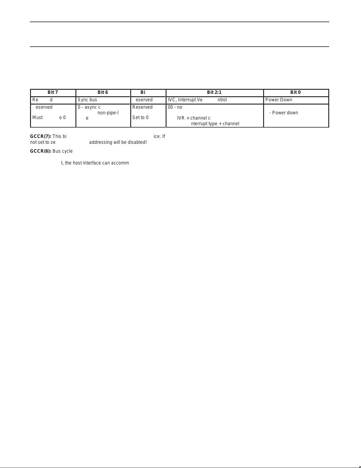
Philips Semiconductors Preliminary specification
Á
Á
Á
Á
Á
Á
Á
Á
Á
Á
SC28L194Quad UART for 3.3V and 5V supply voltage
Table 2. GCCR - Global Configuration Control Register
THIS IS A VERY IMPORTANT REGISTER! IT SHOULD BE THE FIRST REGISTER ADDRESSED DURING INITIALIZATION. This register
has two addresses: x‘0F and x‘8F. The Global Configuration Control Register (GCCR) sets the type of bus cycle, interrupt vector modification
and the power-up or -down mode.
Bit 7
Reserved
Reserved
ÁÁÁÁ
Must be set to 0
ÁÁÁÁ
Sync bus cycles
0 - async cycles
1 - Sync, non-pipe-lined
cycle
Bit 6
БББББ
БББББ
Bit 5:3
Reserved
Reserved
ÁÁÁ
Set to 0
ÁÁÁ
Bit 2:1
IVC, Interrupt Vector Control
00 - no interrupt vector
01 - IVR
ББББББББББ
10 - IVR + channel code
11 - IVR + interrupt type + channel code
ББББББББББ
Bit 0
Power Down Mode
0 - Device enabled
1 - Power down
ББББББ
ББББББ
GCCR(7): This bit is reserved for future versions of this device. If
not set to zero most internal addressing will be disabled!
GCCR(6): Bus cycle selection
Controls the operation of the host interface logic. If reset, the power
on/reset default, the host interface can accommodate arbitrarily long
bus I/O cycles. If the bit is set, the Quad UART expects four Sclk
cycle bus I/O operations similar to those produced by an i80386
processor in non-pipelined mode. The major differences in these
modes are observed in the DACKN pin function. In Sync mode, no
negation of CEN is required between cycles.
GCCR(2:1): Interrupt vector configuration
The IVC field controls if and how the assertion of IACKN (the
interrupt acknowledge pin) will form the interrupt vector for the Quad
UART. If b’00, no vector will be presented during an IACKN cycle.
The bus will be driven high (xFF). If the field contains a b’01, the
contents of the IVR, Interrupt Vector Register, will be presented as
the interrupt vector without modification. If IVC = b’10, the channel
code will replace the 3 LSBs of the IVR; if IVC = b’11 then a modified
interrupt type and channel code replace the 5 LSBs of the IVR.
Note: The modified type field IVR(4:3) is:
10 Receiver w/o error
11 Receiver with error
01 Transmitter
00 All remaining sources
GCCR(0): Power down control
Controls the power down function. During power down the internal
oscillator is disabled, interrupt arbitration and all data
transmission/reception activities cease, and all processing for input
change detection, BRG counter/timers and Address/Xon./Xoff
recognition is disabled.
Note: For maximum power savings it is recommended that all
switching inputs be stopped and all input voltage levels be within 0.5
volt of the Vcc and Vss power supply levels.
To switch from the asynchronous to the synchronous bus cycle
mode, a single write operation to the GCCR, terminated by a
negation of the CEN pin, is required. This cycle may be 4 cycles
long if the setup time of the CEN edge to Sclk can be guaranteed.
The host CPU must ensure that a minimum of two Sclk cycles
elapse before the initiation of the next (synchronous) bus cycle(s).
A hardware or software reset is recommended for the unlikely
requirement of returning to the asynchronous bus cycling mode.
MR - Mode Registers
The user must exercise caution when changing the mode of running
receivers, transmitters or BRG counter/timers. The selected mode
will be activated immediately upon selection, even if this occurs
during the reception or transmission of a character. It is also
possible to disrupt internal controllers by changing modes at critical
times, thus rendering later transmission or reception faulty or
impossible. An exception to this policy is switching from auto-echo
or remote loop back modes to normal mode. If the deselection
occurs just after the receiver has sampled the stop bit (in most
cases indicated by the assertion of the channel’s RxRDY bit) and
the transmitter is enabled, the transmitter will remain in auto-echo
mode until the end of the transmission of the stop bit.
1998 Sep 21
16
Page 17

Philips Semiconductors Preliminary specification
Á
Á
Á
Á
Á
Á
Á
Á
Á
Á
Á
Á
Á
Á
Á
SC28L194Quad UART for 3.3V and 5V supply voltage
Table 3. MR0- Mode Register 0
See “XISR” for more descriptions of MR0 Xon/Xoff functions
Bit 7
Xon/Xoff * transparency
Address Recognition *
transparency
1 - flow control characters
received are pushed onto
БББББ
the RxFIFO
БББББ
0 - flow control characters
received are not pushed
БББББ
onto the RxFIFO
1 - Address characters
received are pushed to
ББББББ
RxFIFO
ББББББ
0 - Address characters
received are not pushed
ББББББ
onto the RxFIFO
* If these bits are not 0 the characters will be stripped regardless of bits (3:2) or (1:0)
MR0[7 & 6] - Control the handling of recognized Xon/Xoff or
Address characters. If set, the character codes are placed on the
RxFIFO along with their status bits just as ordinary characters are. If
the character is not pushed onto the RxFIFO, its received status will
be lost unless the receiver is operating in the block error mode (see
MR1[5] and the general discussion on receiver error handling).
Interrupt processing is not effected by the setting of these bits. See
Character recognition section.
MR0[5:4] - Controls the fill level at which a transmitter begins to
present its interrupt number to the interrupt arbitration logic. Use of a
low fill level minimizes the number of interrupts generated and
maximizes the number of transmit characters per interrupt cycle. It
also increases the probability that the transmitter will go idle for lack
of characters in the TxFIFO.
MR0[3:2] - Controls the Xon/Xoff processing logic. Auto Transmitter
flow control allows the gating of Transmitter activity by Xon/Xoff
characters received by the Channel’s receiver. Auto Receiver flow
control causes the Transmitter to emit an Xoff character when the
RxFIFO has loaded to a depth of 12 characters. Draining the
Bit 6
Bit 5:4
TxINT
TxFIFO interrupt
level control
ÁÁÁ
00 - empty
ÁÁÁ
01 - 3/4 empty
10 - 1/2 empty
ÁÁÁ
11 - not full
Bit 3:2
In-band flow control mode
Address Recognition
Bit 1:0
control
00 - host mode, only the host CPU
may initiate flow control actions
ББББББББ
through the CR
ББББББББ
01 - Auto Transmitter flow control
10 - Auto Receiver flow control
ББББББББ
11 - Auto Rx and Tx flow control
00 - none
01 - Auto wake
ББББББ
10 - Auto doze
ББББББ
11 - Auto wake and auto
doze
ББББББ
RxFIFO to a level of 8 or less causes the Transmitter to emit an Xon
character. All transmissions require no host involvement. A setting
other than b’00 in this field precludes the use of the command
register to transmit Xon/Xoff characters.
Note: Interrupt generation in Xon/Xoff processing is controlled by the
IMR (Interrupt Mask Register) of the individual channels. The
interrupt may be cleared by a read of the XISR, the Xon/Xoff
Interrupt Status Register. Receipt of a flow control character will
always generate an interrupt if the IMR is so programmed. The
MR0[3:2] bits have effect on the automatic aspects of flow control
only, not the interrupt generation.
MR0[1:0] - This field controls the operation of the Address
recognition logic. If the device is not operating in the special or
“wake-up” mode, this hardware may be used as a general purpose
character detector by choosing any combination except b’00.
Interrupt generation is controlled by the channel IMR. The XISR
interrupt and the XISR status bits may be cleared by a read of the
XISR. See further description in the section on the Wake-up mode.
1998 Sep 21
17
Page 18

Philips Semiconductors Preliminary specification
Á
Á
Á
Á
Á
Á
Á
Á
Á
Á
Á
Á
SC28L194Quad UART for 3.3V and 5V supply voltage
Table 4. MR1 - Mode Register 1
Bit 7
RxRTS Control
0 - off
1 - on
ÁÁÁÁ
ÁÁÁÁ
Bit 6
ISR Read Mode
0 - ISR unmasked
1 - ISR masked
БББББ
БББББ
Bit 5
Error Mode
0 = Character
1 = Block
ÁÁÁÁ
ÁÁÁÁ
Bit 4:3
Parity Mode
00 - With Parity
01 - Force parity
БББББ
10 - No parity
11 - Special Mode
БББББ
Bit 2
Parity Type
0 = Even
1 = Odd
ÁÁÁÁ
ÁÁÁÁ
Bit 1:0
Bits per Character
00 - 5
01 - 6
БББББ
10 - 7
11 - 8
БББББ
MR1[7]: Receiver Request to Send Control
This bit controls the deactivation of the RTSN output (I/O2) by the
receiver. This output is asserted and negated by commands applied
via the command register. MR1[7] = 1 causes RTSN to be
automatically negated upon receipt of a valid start bit if the receiver
FIFO is 3/4 full or greater. RTSN is reasserted when an the FIFO fill
level falls below 3/4 full. This constitutes a change from previous
members of Philips (Signets)’ UART families where the RTSN
function triggered on FIFO full. This behavior caused problems with
PC UARTs that could not stop transmission at the proper time. The
RTSN feature can be used to prevent overrun in the receiver, by
using the RTSN output signal, to control the CTSN input of the
transmitting device.
MR1[6]: Interrupt Status Masking
This bit controls the readout mode of the Interrupt Status Register,
ISR. If set, the ISR reads the current status masked by the IMR, i.e.
only interrupt sources enabled in the IMR can ever show a ‘1’ in the
ISR. If cleared, the ISR shows the current status of the interrupt
source without regard to the Interrupt Mask setting.
MR1[5]: Error Mode Select
This bit selects the operating mode of the three FIFOed status bits
(FE, PE, received break). In the character mode, status is provided
on a character by character basis; the status applies only to the
character at. the bottom of the FIFO. In the block mode, the status
provided in the SR for these bits is the accumulation (logical OR) of
the status for all characters coming to the top of the FIFO, since the
last reset error command was issued.
MR1[4:3]: Parity Mode Select
If ‘with parity’ or ’force parity’ is selected, a parity bit is added to the
transmitted character and the receiver performs a parity check on
incoming data. MR1[4:3] = 11 selects the channel to operate in the
special Wake-up mode.
MR1[2]: Parity Type Select
This bit sets the parity type (odd or even) if the ’with parity’ mode is
programmed by MR1[4:3], and the polarity of the forced parity bit if
the ’force parity’ mode is programmed. It has no effect if the ’no
parity’ mode is programmed. In the special ’Wake-up’ mode, it
selects the polarity of the A/D bit. The parity bit is used to an
address or data byte in the ’Wake-up’ mode.
MR1[1:0]: Bits per Character Select
This field selects the number of data bits per character to be
transmitted and received. This number does not include the start,
parity, or stop bits.
1998 Sep 21
18
Page 19

Philips Semiconductors Preliminary specification
Á
Á
Á
Á
Á
SC28L194Quad UART for 3.3V and 5V supply voltage
Table 5. MR2 - Mode Register 2
The MR2 register provides basic channel setup control that may need more frequent updating.
Bits 7:6
Channel Mode
00 = normal
01 = Auto echo
10 = Local loop
БББББ
11 = Remote loop
TxRTS Control
0 = No
1 = Yes
ББББББ
Bit 5
Bit 4
CTSN Enable Tx
0 = No
1 = Yes
ББББББ
Bit 3:2
RxINT
00 = RRDY
01 = Half Full
10 = 3/4 Full
БББББ
11 = Full
Bit 1:0
Stop Length
00 = 1.0
01 = 1.5
10 = 2.0
ББББББ
11 = 9/16
MR2[7:6] - Mode Select
The Quad UART can operate in one of four modes: MR2[7:6] = b’00
is the normal mode, with the transmitter and receiver operating
independently.
MR2[7:6] = b’01 places the channel in the automatic echo mode,
which automatically re transmits the received data. The following
conditions are true while in automatic echo mode:
Received data is re-clocked and re-transmitted on the TxD
output.
The receive clock is used for the transmitter.
The receiver must be enabled, but the transmitter need not be
enabled.
The TxRDY and TxEMT status bits are inactive.
The received parity is checked, but is not regenerated for
transmission, i.e., transmitted parity bit is as received.
Character framing is checked, but the stop bits are retransmitted
as received.
A received break is echoed as received until the next valid start
bit is detected.
CPU to receiver communication continues normally, but the CPU to
transmitter link is disabled.
Two diagnostic modes can also be selected.
MR2[7:6] = b’10 selects local loop back mode. In this mode:
The transmitter output is internally connected to the receiver
input.
The transmit clock is used for the receiver.
The TxD output is held high.
The RxD input is ignored.
The transmitter must be enabled, but the receiver need not be
enabled.
CPU to transmitter and receiver communications continue
normally .
The second diagnostic mode is the remote loop back mode,
selected by MR2[7:6] = b’11. In this mode:
Received data is re-clocked and re-transmitted on the TxD
output.
The receive clock is used for the transmitter.
Received data is not sent to the local CPU, and the error status
conditions are inactive.
The received parity is not checked and is not regenerated for
transmission, i.e., the transmitted parity bit is as received.
The receiver must be enabled, but the transmitter need not be
enabled.
Character framing is not checked, and the stop bits are
retransmitted as received.
A received break is echoed as received until the next valid start
bit is detected.
MR2[5] - Transmitter Request to Send Control
This bit controls the deactivation of the RTSN output (I/O2) by the
transmitter. This output is manually asserted and negated by
appropriate commands issued via the command register. MR2[5] = 1
causes RTSN to be reset automatically one bit time after the
characters in the transmit shift register and in the TxFIFO (if any)
are completely transmitted (includes the programmed number of
stop bits if the transmitter is not enabled). This feature can be used
to automatically terminate the transmission of a message as follows:
Program auto reset mode: MR2[5]= 1.
Enable transmitter.
Assert RTSN via command.
Send message.
After the last character of the message is loaded to the TxFIFO,
disable the transmitter. Before disabling the transmitter be sure
the Status Register TxEMT bit is NOT set (i.e., the transmitter is
not underrun). The underrun condition is indicated by the TxEMT
bit in the SR being set. The codition occurs immediately upon
enabling the transmitter and persists until a character is loaded
to the TxFIFO. The Underrun condition will not be a problem as
long as the controlling processor keeps up with the transmitter
data flow. The proper operation of this feature assumes that the
transmitter is busy (not underrun) when the disable is issued.
The last character will be transmitted and RTSN will be reset one
bit time after the last stop bit.
NOTE: When the transmitter controls the RTSN pin, the meaning of
the pin is COMPLETELY changed. It has nothing to do with the
normal RTSN/CTSN “handshaking”. It is usually used to mean “end
of message” and to “turn the line around” in simplex
communications.
MR2[4] - Clear to Send Control
The state of this bit determines if the CTSN input (I/O0) controls the
operation of the transmitter. If this bit is 0, CTSN has no effect on the
transmitter. If this bit is a 1, the transmitter checks the state of CTSN
each time it is ready to begin sending a character. If it is asserted
(low), the character is transmitted. If it is negated (high), the TxD
output remains in the marking state and the transmission is delayed
until CTSN goes low. Changes in CTSN, while a character is being
transmitted, do not affect the transmission of that character. This
feature can be used to prevent overrun of a remote receiver.
MR2[3:2] - RxINT control field
Controls when interrupt arbitration for a receiver begins based on
RxFIFO fill level. This field allows interrupt arbitration to begin when
the RxFIFO is full, 3/4 full, 1/2 full or when it contains at least 1
character.
MR2[1:0] - Stop Bit Length Select
This field programs the length of the stop bit appended to the
transmitted character. Stop bit lengths of 9/16, 1, 1.5 and 2 bits can
be programmed for character lengths of 6, 7, and 8 bits. For a
character length of 5 bits, 1, 1.5 and 2 stop bits can be programmed.
In all cases, the receiver only checks for a mark condition at the
center of the first stop bit position (one bit time after the last data bit,
or after the parity bit if parity is enabled). If an external 1X clock is
used for the transmitter, MR2[1] = 0 selects one stop bit and
MR2[1] = 1 selects two stop bits to be transmitted.
1998 Sep 21
19
Page 20

Philips Semiconductors Preliminary specification
Á
Á
Á
Á
Á
Á
Á
Á
SC28L194Quad UART for 3.3V and 5V supply voltage
Table 6. RxCSR and TxCSR - Receiver and Transmitter Clock Select Registers
Both registers consist of single 5 bit field that selects the clock source for the receiver and transmitter, respectively. The unused bits in this
register read b’000. The baud rates shown in the table below are based on the x1 crystal frequency of 3.6864MHz. The baud rates shown below
will vary as the X1 crystal clock varies. For example, if the X1 rate is changed to 7.3728 MHz all the rates below will double.
Bits 7:5
Reserved
Transmitter/Receiver Clock select code, (see Clock Mux Table below)
Table 7. Data Clock Mux
CCLK maximum rate is 8MHz. Data clock rates will follow exactly the ratio of CCLK to 3.6864MHz.
Clock Select Code
Bits 4:0
БББББ
00000
00001
00010
0001 1
00100
00101
00110
00111
01000
01001
01010
0101 1
01100
01101
01110
01111
БББББББББ
Clock selection,
CCLK = 3.6864 MHz
BRG - 50
BRG - 75
BRG - 150
BRG - 200
BRG - 300
BRG - 450
BRG - 600
BRG - 900
BRG - 1200
BRG - 1800
BRG - 2400
BRG - 3600
BRG - 4800
BRG - 7200
BRG - 9600
BRG - 14.4K
Clock Select Code
БББББ
10000
10001
10010
1001 1
10100
10101
10110
10111
11000
11001
11010
11011
11100
11101
11110
11111
Bits 4:0
Clock selection,
ББББББББББ
CCLK = 3.6864 MHz
BRG - 19.2K
BRG - 28.8K
BRG - 38.4K
BRG - 57.6K
BRG - 115.2K
BRG - 230.4K
Gin0
Gin1
BRG C/T 0
BRG C/T 1
Reserved
I/O2 rcvr, I/O3 xmit -16x
I/O2 rcvr, I/O3 xmit-1x
Reserved
Reserved
Reserved
Table 8. CR - Command Register
CR is used to write commands to the Quad UART.
Bits 7:3
Channel Command codes see
ББББББББ
“Command Register Table”
1 = Hold present condition of Tx & Rx Enables
БББББББББББ
0 = Change Tx & Rx enable conditions
CR[2] - Lock TxD and RxFIFO enables
If set, the transmitter and receiver enable bits, CR[1:0] are not
significant. The enabled/disabled state of a receiver or transmitter
can be changed only if this bit is at zero during the time of the write
to the command register. WRITES TO THE UPPER BITS OF THE
CR WOULD USUALLY HAVE CR[2] AT 1 to maintain the condition
of the receiver and transmitter. The bit provides a mechanism for
writing commands to a channel, via CR[7:3], without the necessity of
keeping track of or reading the current enable status of the receiver
and transmitter.
CR[1] - Enable Transmitter
A one written to this bit enables operation of the transmitter. The
TxRDY status bit will be asserted. When disabled by writing a zero
to this bit, the command terminates transmitter operation and resets
the TxRDY and TxEMT status bits. However, if a character is being
transmitted or if characters are loaded in the TxFIFO when the
transmitter is disabled, the transmission of the all character(s) is
completed before assuming the inactive state.
CR[0] - Enable Receiver
A one written to this bit enables operation of the receiver. If not in
the special Wake-up mode, this also forces the receiver into the
search for start bit state. If a zero is written, this command
terminates operation of the receiver immediately - a character being
Bit 2
Bit 1
1 = Enable Tx
БББББ
0 = Disable Tx
1 = Enable Rx
0 = Disable Rx
Bit 0
БББББ
received will be lost. The command has no effect on the receiver
status bits or any other control registers. If the special wake-up
mode is programmed, the receiver operates even if it is disabled
(see Wake-up Mode).
CR[7:3] - Miscellaneous Commands (See Table below) The encoded value of this field can be used to specify a single command as follows: 00000 No command. 00001 Reserved. 00010 Reset receiver. Resets the receiver as if a hardware reset
had been applied. The receiver is disabled and the FIFO
pointer is reset to the first location effectively discarding all
unread characters in the FIFO.
0001 1 Reset transmitter. Resets the transmitter as if a hardware
reset had been applied.
00100 Reset error status. Clears the received break, parity error,
framing error, and overrun error bits in the status register
(SR[7:4]). Used in character mode to clear overrun error
status (although RB, PE and FE bits will also be cleared),
and in block mode to clear all error status after a block of
data has been received.
00101 Reset break change interrupt. Causes the break detect
change bit in the interrupt status register (ISR[2]) to be
cleared to zero.
1998 Sep 21
20
Page 21

Philips Semiconductors Preliminary specification
SC28L194Quad UART for 3.3V and 5V supply voltage
00110 Start break. Forces the TxD output low (spacing). If the
transmitter is empty, the start of the break condition will be
delayed up to two bit times. If the transmitter is active, the
break begins when transmission of the current character
is completed. If there are characters in the TxFIFO, the
start of break is delayed until those characters, or any
others loaded after it have been transmitted (TxEMT must
be true before break begins). The transmitter must be
enabled to start a break.
00111 Stop break. The TxD line will go high (marking) within two
bit times. TxD will remain high for one bit time before the
next character, if any, is transmitted.
01000 Assert RTSN. Causes the RTSN output to be asserted
(low).
01001 Negate RTSN. Causes the RTSN output to be negated
(high).
Note: The two commands above actually reset and
set, respectively, the I/O2 or I/O1 pin associated with
the I/OPIOR register.
01010 Reserved.
0101 1 Reserved.
01100 Reserved.
01101 Block error status mode. Upon reset of the device or an
individual receiver, the block mode of receiver error status
accumulates as each character moves to the bottom of
the RxFIFO, the position from which it will be read. In this
mode of operation, the RxFIFO may contain a character
with non-zero error status for some time. The status will
not reflect the error character’s presence until it is ready to
be popped from the RxFIFO. Command 01101 allows the
error status to be updated as each character is pushed
into the RxFIFO. This allows the earliest detection of a
problem character, but complicates the determination of
exactly which character is causing the error. This mode of
block error accumulation may be exited only by resetting
the chip or the individual receiver.
0111 1 Reserved.
10000 Transmit an Xon Character
10001 Transmit an Xoff Character
10010 Reserved for channels b-d, for channel a: enables a Gang
Write of Xon Character Registers. After this command is
issued, a write to the channel A Xon Character Register
will result in a write to all channel’s Xon character
registers. This command provides a mechanism to
initialize all the Xon Character registers with one write. A
write to channel A Xon Character Register returns the
Quad UART to the individual Xon write mode.
1001 1 Reserved for channels b-d, for channel a: enables Gang
Write of Xoff Character Registers. After this command is
issued, a write to the channel A Xoff Character Register
will result in a write to all channel’s Xoff character
registers. This command provides a mechanism to
initialize all the Xoff Character registers with one write. A
write to channel A Xoff Character Register returns the
Quad UART to the individual Xoff write mode.
Note: Gang writing of Xon/Xoff Character Commands: Issuing
command causes the next write to Xon/Xoff Character Register
A to effect a simultaneous write into the other 3 Xon/Xoff
character registers. After the Xon/Xoff Character Register A is
written, the 28L194 returns to individual write mode for the
Xon/Xoff Character Registers. Other intervening reads and
writes are ignored. The device resets to individual write mode.
10100 Reserved for channels b-d, for channel a: executes a
Gang Load of Xon Character Registers. Executing this
command causes a write of the value x’11 to all channel’s
Xon character registers. This command provides a
mechanism to initialize all the Xon Character registers to a
default value with one write. Execution of this command is
immediate and does not effect the timing of subsequent
host I/O operations.
10101 Reserved for channels b-d, for channel a: executes a
Gang Load of Xoff Character Registers. Executing this
command causes a write of the value x’13 to all channel’s
Xoff character registers. This command provides a
mechanism to initialize all the Xoff Character registers to a
default value with one write. Execution of this command is
immediate and does not effect the timing of subsequent
host I/O operations.
10110 Xoff resume command (CRXoffre; not active in
“Auto-Transmit Mode”). A command to cancel a previous
Host Xoff command. Upon receipt, the channel’s
transmitter will transfer a character, if any, from the
TxFIFO and begin transmission.
10111 Host Xoff command (CRXoff). This command allows tight
host CPU control of the flow control of the channel
transmitter. When interrupted for receipt of an Xof f
character by the receiver, the host may stop transmission
of further characters by the channel transmitter by issuing
the Host Xoff command. Any character that has been
transferred to the TxD shift register will complete its
transmission, including the stop bit.
11000 Cancel Host transmit flow control command. Issuing this
command will cancel a previous transmit command if the
flow control character is not yet loaded into the TxD Shift
Register. If there is no character waiting for transmission
or if its transmission has already begun, then this
command has no effect.
11001-11011
Reserved.
11011 Reset Address Recognition Status. This command clears
the interrupt status that was set when an address
character was recognized by a disabled receiver
operating in the special mode.
11100-1 1101
Reserved.
11110 Resets all UART channel registers. This command
provides a means to zero all the UART channels that are
not reset to x’00 by a reset command or a hardware reset.
11111 Reserved for channels b-d, for channel a: executes a chip
wide reset. Executing this command in channel a is
equivalent to a hardware reset with the RESETN pin.
Executing command register reset in channel b-d, has no
effect.
1998 Sep 21
21
Page 22

Philips Semiconductors Preliminary specification
ББББББББББББББ
ББББББББББББББ
ББББББББББББББ
ББББББББББББББ
ББББББББББББББ
ББББББББББББББ
ББББББББББББББ
ББББББББББББББ
ББББББББББББББ
ББББББББББББББ
ББББББББББББББ
ББББББББББББББ
ББББББББББББББ
ББББББББББББББ
ББББББББББББББ
Á
Á
Á
Á
Á
Á
БББББ
Á
Á
Á
БББББ
SC28L194Quad UART for 3.3V and 5V supply voltage
Table 9. Command Register Code
Commands x’12, x13, x’14, x’15, x’1f (marked with*) are global and exist only in channel A ’s register space.
Channel Command
Code
CR[7:3]
00000
00001
00010
0001 1
00100
00101
00110
00111
01000
01001
01010
0101 1
01100
01101
01110
01111
Reset Break Change Interrupt
Assert RTSN (I/O2 or I/O1)
Negate RTSN (I/O2 or I/O1)
Block Error Status configure
Channel
Command
Description
NOP
Reserved
Reset Receiver
Reset Transmitter
Reset Error Status
Begin Transmit Break
End Transmit Break
Set time-out mode on
Reserved
Set time-out mode off
Reserved
Reserved
Channel Command
Code
CR[7:3]
10000
10001
10010
1001 1
10100
10101
10110
10111
11000
11001
11010
11011
11100
11101
11110
11111
Channel
Command
Description
Transmit Xon
Transmit Xoff
Gang Write Xon Character Registers *
Gang Write Xoff Character Registers *
Gang Load Xon Character Registers DC1 *
Gang Load Xoff Character Registers DC3 *
Xoff Resume Command
Host Xoff Command
Cancel Transmit X Char command
Reserved
Reserved
Reset Address Recognition Status
Reserved
Reserved
Reset All UART channel registers
Reset Device *
Table 10. SR - Channel Status Register
Bit 7
Received
ÁÁÁ
Break
0 - No
1 - Yes
SR[7] - Received Break
This bit indicates that an all zero character of the programmed
length has been received without a stop bit. Only a single FIFO
position is occupied when a break is received; further entries to the
FIFO are inhibited until the RxD line returns to the marking state for
at least one half bit time (two successive edges of the internal or
external 1x clock). When this bit is set, the change in break bit in the
ISR (ISR[2]) is set. ISR[2] is also set when the end of the break
condition, as defined above, is detected. The break detect circuitry
is capable of detecting breaks that originate in the middle of a
received character. However, if a break begins in the middle of a
character, it must last until the end of the next character in order for
it to be detected.
SR[6] - Framing Error (FE)
This bit, when set, indicates that a stop bit was not detected when
the corresponding data character in the FIFO was received. The
stop bit check is made in the middle of the first stop bit position.
SR[5] - Parity Error (PE)
This bit is set when the ’with parity’ or ’force parity’ mode is
programmed and the corresponding character in the FIFO was
received with incorrect parity. In the special ’Wake-up mode’, the
parity error bit stores the received A/D bit.
SR[4] - Overrun Error (OE)
This bit, when set, indicates that one or more characters in the
received data stream have been lost. It is set upon receipt of a new
character when the RxFIFO is full and a character is already in the
receive shift register waiting for an empty FIFO position. When this
occurs, the character in the receive shift register (and its break
detect, parity error and framing error status, if any) is lost. This bit is
cleared by a reset error status command.
Bit 6
Framing Error
ÁÁÁ
0 - No
1 - Yes
Bit 5
Parity
ÁÁÁ
Error
0 - No
1 - Yes
Bit 4
Overrun Error
ÁÁÁ
0 - No
1 - Yes
Bit 3
TxEMT
ÁÁÁ
0 - No
1 - Yes
Bit 2
TxRDY
ÁÁÁÁ
0 - No
1 - Yes
Bit 1
RxFULL
ÁÁÁ
0 - No
1 - Yes
Bit 0
RxRDY
ÁÁÁ
0 - No
1 - Yes
SR[3] - Transmitter Empty (TxEMT)
This bit is set when the transmitter underruns, i.e., both the TxFIFO
and the transmit shift register are empty.
It is set after transmission of the last stop bit of a character, if no
character is in the TxFIFO awaiting transmission. It is reset when the
TxFIFO is loaded by the CPU, or when the transmitter is disabled.
SR[2] - Transmitter Ready (TxRDY)
This bit, when set, indicates that the TxFIFO is ready to be loaded
with a character. This bit is cleared when the TxFIFO is loaded by
the CPU and is set when the last character is transferred to the
transmit shift register. TxRDY is reset when the transmitter is
disabled and is set when the transmitter is first enabled, e.g.,
characters loaded in the TxFIFO while the transmitter is disabled will
not be transmitted.
SR[1] - RxFIFO Full (RxFULL)
This bit is set when a character is transferred from the receive shift
register to the receive FIFO and the transfer causes the FIFO to
become full, i.e., all sixteen RxFIFO positions are occupied. It is
reset when the CPU reads the RxFIFO and that read leaves one
empty byte position. If a character is waiting in the receive shift
register because the RxFIFO is full, RxFULL is not reset until the
second read of the RxFIFO since the waiting character is
immediately loaded to the RxFIFO.
SR[0] - Receiver Ready (RxRDY)
This bit indicates that a character has been received and is waiting
in the RxFIFO to be read by the CPU. It is set when the character is
transferred from the receive shift register to the RxFIFO and reset
when the CPU reads the RxFIFO, and no more characters are in the
RxFIFO.
1998 Sep 21
22
Page 23

Philips Semiconductors Preliminary specification
Á
Á
Á
Á
Á
Á
Á
Á
SC28L194Quad UART for 3.3V and 5V supply voltage
Table 11. ISR - Interrupt Status Register
Bit 7
I/O Port
change of
ÁÁ
state
Bit 6
Receiver
Watch-dog
ÁÁ
Time-out
Bit 5
Address
recognition event
ÁÁÁÁ
Bit 4
Xon/off
event
Á
Bit 3
Always 0
ÁÁÁ
Bit 2
Change of
Break State
ÁÁÁ
Bit 1
RxRDY
Receiver has entered
ÁÁÁÁ
arbitration process
Bit 0
TxRDY
Transmitter has entered
ББББББ
arbitration process
This register provides the status of all potential interrupt sources for
a UART channel. When generating an interrupt arbitration value, the
contents of this register are masked by the interrupt mask register
(IMR). If a bit in the ISR is a ’1’ and the corresponding bit in the IMR
is also a ’1’, interrupt arbitration for this source will begin. If the
corresponding bit in the IMR is a zero, the state of the bit in the ISR
can have no affect on the IRQN output. Note that the IMR may or
may not mask the reading of the ISR as determined by MR1[6]. If
MR1[6] is cleared, the reset and power on default, the ISR is read
without modification. If MR1[6] is set, the a read of the ISR gives a
value of the ISR ANDed with the IMR.
ISR[7] - Input Change of State
This bit is set when a change of state occurs at the I/O1 or I/O0
input pins. It is reset when the CPU reads the Input Port Register,
IPR.
ISR[6] Watch-dog Time-out
This bit is set when the receiver’s watch-dog timer has counted
more than 64 bit times since the last RxFIFO event. RxFIFO events
are a read of the RxFIFO or GRxFIFO, or the push of a received
character into the FIFO. The interrupt will be cleared automatically
upon the push of the next character received or when the RxFIFO or
GRxFIFO is read. The receiver watch-dog timer is included to allow
detection of the very last characters of a received message that may
be waiting in the RxFIFO, but are too few in number to successfully
initiate an interrupt. Refer to the watch-dog timer description for
details of how the interrupt system works after a watch-dog time-out.
ISR[5] - Address Recognition Status Change
This bit is set when a change in receiver state has occurred due to
an Address character being received from an external source and
comparing to the reference address in ARCR. The bit and interrupt
is negated by a write to the CR with command x11011, Reset
Address Recognition Status.
ISR[4] - Xon/Xoff Status Change
This bit is set when an Xon/Xoff character being received from an
external source. The bit is negated by a read of the channel Xon
Interrupt Status Register, XISR.
ISR[3] - Reserved Always reads a 0 ISR[2] - Change in Channel Break Status
This bit, when set, indicates that the receiver has detected the
beginning or the end of a received break. It is reset when the CPU
issues a reset break change interrupt command via the CR.
ISR[1] - Receiver Ready
The general function of this bit is to indicate that the RxFIFO has
data available. The particular meaning of this bit is programmed by
MR2[3:2]. If programmed as receiver ready(MR2[3:2] = 00), it
indicates that at least one character has been received and is
waiting in the RxFIFO to be read by the host CPU. It is set when the
character is transferred from the receive shift register to the RxFIFO
and reset when the CPU reads the last character from the RxFIFO.
If MR2[3:2] is programmed as FIFO full, ISR[1] is set when a
character is transferred from the receive holding register to the
RxFIFO and the transfer causes the RxFIFO to become full, i.e. all
sixteen FIFO positions are occupied. It is reset when ever RxFIFO is
not full. If there is a character waiting in the receive shift register
because the FIFO is full, the bit is set again when the waiting
character is transferred into the FIFO.
The other two conditions of these bits, 3/4 and half full operate in a
similar manner. The ISR[1] bit is set when the RxFIFO fill level
meets or exceeds the value; it is reset when the fill level is less. See
the description of the MR2 register.
Note: This bit must be at a one (1) for the receiver to enter the
arbitration process. It is the fact that this bit is zero (0) when the
RxFIFO is empty that stops an empty FIFO from entering the
interrupt arbitration. Also note that the meaning if this bit is not quite
the same as the similar bit in the status register (SR).
ISR[0] - Transmitter Ready
The general function of this bit is to indicate that the TxFIFO has an
at least one empty space for data. The particular meaning of the bit
is controlled by MR0[5:4] indicates the TxFIFO may be loaded with
one or more characters. If MR0[5:4] = 00 (the default condition) this
bit will not set until the TxFIFO is empty - sixteen bytes available. If
the fill level of the TxFIFO is below the trigger level programmed by
the TxINT field of the Mode Register 0, this bit will be set. A one in
this position indicates that at least one character can be sent to the
TxFIFO. It is turned off as the TxFIFO is filled above the level
programmed by MR0[5:4. This bit turns on as the FIFO empties; the
RxFIFO bit turns on as the FIFO fills. This often a point of confusion
in programming interrupt functions for the receiver and transmitter
FIFOs.
Note: This bit must be at a one (1) for the transmitter to enter the
arbitration process. It is the fact that this bit is zero (0) when the
RxFIFO is full that stops a full FIFO from entering the interrupt
arbitration. Also note that the meaning if this bit is not quite the same
as the similar bit in the status register (SR).
1998 Sep 21
23
Page 24

Philips Semiconductors Preliminary specification
Á
Á
Á
Á
Á
Á
Á
Á
Á
Á
Á
Á
БББББББББББ
БББББББББББ
SC28L194Quad UART for 3.3V and 5V supply voltage
Table 12. IMR - Interrupt Mask Register
Bit 7
I/O Port change
of state
ÁÁÁ
Bit 6
Receiver Watch-dog
Time-out
БББББ
Bit 5
Address
recognition event
ÁÁÁÁ
Bit 4
Xon/off event
ÁÁÁ
Bit 3
Set to 0
Á
Bit 2
Change of
Break State
ÁÁÁ
Bit 1
RxRDY
interrupt
ÁÁÁ
Bit 0
TxRDY
interrupt
ÁÁÁ
The programming of this register selects which bits in the ISR cause
an interrupt output. If a bit in the ISR is a ’1’ and the corresponding
bit in the IMR is a ’1’, the interrupt source is presented to the internal
interrupt arbitration circuits, eventually resulting in the IRQN output
being asserted (low). If the corresponding bit in the IMR is a zero,
the state of the bit in the ISR has no affect on the IRQN output.
IMR[7] - Controls if a change of state in the inputs equipped with
input change detectors will cause an interrupt.
IMR[6] - Controls the generation of an interrupt by the watch-dog
timer event. If set, a count of 64 idle bit times in the receiver will
begin interrupt arbitration.
IMR[5] - Enables the generation of an interrupt in response to
changes in the Address Recognition circuitry of the Special Mode
(multi-drop or wake-up mode).
IMR[4] - Enables the generation of an interrupt in response to
recognition of an in-band flow control character.
IMR[3] - Reserved
IMR[2] - Enables the generation of an interrupt when a Break
condition has been detected by the channel receiver.
IMR[1] - Enables the generation of an interrupt when servicing for
the RxFIFO is desired.
IMR[0] - Enables the generation of an interrupt when servicing for
the TxFIFO is desired.
Table 13. RxFIFO Receiver FIFO
Bit[10]
Break
Received
Status
ÁÁ
The FIFO for the receiver is 11 bits wide and 16 “words” deep. The
status of each byte received is stored with that byte and is moved
along with the byte as the characters are read from the FIFO. The
upper three bits are presented in the STATUS register and they
change in the status register each time a data byte is read from the
FIFO. Therefor the status register should be read BEFORE the byte
is read from the RxFIFO if one wishes to ascertain the quality of the
byte
The forgoing applies to the “character error” mode of status
reporting. See MR1[5] and “RxFIFO Status” descriptions for “block
error” status reporting. Briefly “Block Error” gives the accumulated
error of all bytes received in the RxFIFO since the last “Reset Error”
command was issued. (CR = x’04)
Bit[9]
Framing
Error
Status
ÁÁ
Bit[8]
Parity
Error
Status
ÁÁ
Bits [7:0]
8 data bits
MSBs =0 for 7,6,5 bit
ББББББ
data
Table 14. TxFIFO - Transmitter FIFO
Bits 7:0
8 data bits. MSBs set to 0 for 7, 6, 5 bit data
The FIFO for the transmitter is 8 bits wide by 16 bytes deep. For
character lengths less than 8 bits the upper bits will be ignored by
the transmitter state machine and thus are effectively discarded.
Table 15. BCRBRK - Bidding Control Register -
Break Change
Bits 7:3
Reserved
MSB of break change interrupt bid
This register provides the 3 MSBs of the Interrupt Arbitration number
for a break change interrupt.
Bits 2:0
Table 16. BCRCOS - Bidding Control Register -
Change of State
Bits 7:3
Reserved
MSB of a COS interrupt bid
Read as x’0
This register provides the 3 MSBs of the Interrupt Arbitration number
for a Change of State, COS, interrupt.
Bits 2:0
Table 17. BCRx - Bidding Control Register -
Xon/Xoff
Bits 7:3
Reserved
MSB of an Xon/Xoff interrupt bid
This register provides the 3 MSBs of the Interrupt Arbitration number
for an Xon/Xoff interrupt.
Bits 2:0
Table 18. BCRA - Bidding Control Register -
Address
Bits 7:3
Reserved
MSB of an address recognition event
interrupt bid
This register provides the 3 MSBs of the Interrupt Arbitration number
for an address recognition event interrupt.
Bits 2:0
Table 19. XonCR - Xon Character Register
Bits 7:0
8 Bits of the Xon Character Recognition
An 8 bit character register that contains the compare value for an
Xon character.
Table 20. XoffCR - Xoff Character Register
Bits 7:0
8 Bits of the Xoff Character Recognition
An 8 bit character register that contains the compare value for an
Xoff character .
Table 21. ARCR - Address Recognition Character
Register
Bits 7:0
8 Bits of the Multi-Drop Address Character Recognition
An 8 bit character register that contains the compare value for the
wake-up address character.
1998 Sep 21
24
Page 25

Philips Semiconductors Preliminary specification
Á
Á
Á
Á
Á
Á
Á
Á
Á
Á
Á
Á
Á
SC28L194Quad UART for 3.3V and 5V supply voltage
Table 22. XISR - Xon-Xoff Interrupt Status Register
See MR0 for a description of enabling these functions
Bits 7:6
Received X Character
Status
00 - none
01 - Xoff received
ББББББ
10 - Xon received
ББББББ
11 - both received
Automatic X Character
transmission status
00 - none
01 - Xon transmitted
ББББББББ
10 - Xoff transmitted
ББББББББ
11 - Illegal, does not occur
NOTE: Bits of this register may be cleared by a read of the register.
XISR[7:6] - Received X Character Status. This field can be read to
determine if the receiver has encountered an Xon or Xoff character
in the incoming data stream. These bits are maintained until a read
of the XISR. The field is updated by X character reception
regardless of the state of MR0(7, 3:2) or IMR(4). The field can
therefore be used as a character detector for the bit patterns stored
in the Xon and Xoff Character Registers.
XISR[5:4] - Automatic transmission Status. This field indicates the
last flow control character sent in the Auto Receiver flow control
mode. If Auto Receiver mode has not been enabled, this field will
always read b’00. It will likewise reset to b’00 if MR0(3) is reset. If
the Auto Receiver mode is exited while this field reads b’10, it is the
user’s responsibility to transmit an Xon, when appropriate.
XISR[3:2] - TxD flow Status. This field tracks the transmitter’s flow
status as follows:
00 - normal. The flow control is under host control.
01 - TxD halt pending. After the current character finishes the
transmitter will stop. The status will then change to b’00.
10 - re-enabled. The transmitter had been halted and restarted. It
is sending data characters. After a read of the XISR, it will return
to “normal” status.
11 - disabled. The transmitter is flow controlled.
XISR[1:0] - TxD character Status. This field allows determination of
the type of character being transmitted. If XISR(1:0) is b’01, the
channel is waiting for a data character to transfer from the TxFIFO.
This condition will only occur for a bit time after an Xon or Xoff
character transmission unless the TxFIFO is empty.
Bits 5:4
Bits 3:2
TxD flow status
00 - normal
01 - TxD halt pending
ББББББ
10 - re-enabled
ББББББ
11 - flow disabled
TxD character status
00 - normal TxD data
01 - wait on normal data
БББББББББ
10 - Xoff in pending
БББББББББ
11 - Xon in pending
Bits 1:0
Table 23. WDTRCR - Watch-dog Run Control
Register
Bits 7:4
Reserved
ÁÁ
This register enables the watch-dog Timer for each of the 4
receivers on the Quad UART
Bit 3
WDT d
1 on
ÁÁ
0 off
Bit 2
WDT c
1 on
ÁÁÁ
0 off
Bit 1
WDT b
1 on
ÁÁ
0 off
Table 24. BRGTRU - BRG Timer Reload
Registers, Upper (Timers A & B)
Bits 7:0
8 MSB of the BRG Timer divisor.
This is the upper byte of the 16 bit value used by the BRG timer in
generating a baud rate clock
Table 25. BRGTRL - BRG Timer Reload
Registers, Lower (Timers A & B)
Bits 7:0
8 LSB of the BRG Timer divisor.
This is the lower byte of the 16 bit value used by the BRG timer in
generating a baud rate clock.
Bit 0
WDT a
1 on
ÁÁ
0 off
1998 Sep 21
25
Page 26

Philips Semiconductors Preliminary specification
БББББББББ
БББББББББ
Á
Á
Á
Á
Á
Á
Á
Á
Á
Á
Á
Á
БББББББББ
Á
Á
Á
Á
Á
Á
Á
Á
Á
Á
Á
Á
Á
Á
Á
Á
Á
Á
Á
Á
Á
Á
Á
Á
Á
Á
Á
Á
Á
Á
Á
Á
Á
Á
Á
SC28L194Quad UART for 3.3V and 5V supply voltage
Table 26. BRGTCR - BRG Timer Control Register (BRGTCR)
Bit 7
BRGTCR b, Register control
0 - Resets the timer register and
holds it stopped
БББББББ
1 - Allows the timer register to
БББББББ
БББББББ
БББББББ
run.
BRGTCR b, Clock selection
000 - Sclk / 16
001 - Sclk / 32
БББББББ
010 - Sclk/ 64
011 - Sclk / 128
БББББББ
100 - X1
БББББББ
101 - X1 / 2
110 - I/O1b
БББББББ
111 - Gin(1)
Bit 6:4
Bit 3
BRGTCR a, Register control
0 - Resets the timer register and
ББББББББ
ББББББББ
ББББББББ
ББББББББ
holds it stopped.
1 - Allows the timer register to
run.
Bit 2:0
BRGTCR a, Clock selection
000 - Sclk / 16
001 - Sclk / 32
БББББББ
010 - Sclk / 64
011 - Sclk / 128
БББББББ
100 - X1
БББББББ
101 - X1 / 2
110 - I/O1a
БББББББ
111 - Gin(0)
Start/Stop control and clock select register for the two BRG
counters. The clock selection is for the input to the counters. It is
that clock divided by the number represented by the BRGTU and
BRGTL the will be used as the 16x clock for the receivers and
transmitters. When the BRG timer Clock is selected for the
receiver(s) or transmitter(s) the receivers and transmitters will
consider it as a 16x clock and further device it by 16. In other words
the receivers and transmitters will always be in the 16x mode of
operation when the internal BRG timer is selected for their clock.
(See equation on page 6.)
Table 27. ICR - Interrupt Control Register
Bit 7
Reserved. Set to 0
This register provides a single 7 bit field called the interrupt
threshold for use by the interrupt arbiter. The field is interpreted as a
single unsigned integer. The interrupt arbiter will not generate an
external interrupt request, by asserting IRQN, unless the value of
the highest priority interrupt exceeds the value of the interrupt
threshold. If the highest bidder in the interrupt arbitration is lower
than the threshold level set by the ICR, the Current Interrupt
Register, CIR, will contain x’00. Refer to the functional description of
interrupt generation for details on how the various interrupt source
bid values are calculated.
Note: While a watch-dog Timer interrupt is pending, the ICR is not
used and only receiver codes are presented for interrupt arbitration.
This allows receivers with very low count values (perhaps below the
threshold value) to win interrupt arbitration without requiring the user
to explicitly lower the threshold level in the ICR. These bits are the
upper seven (7) bits of the interrupt arbitration system. The lower
three (3) bits represent the channel number.
UCIR - Update CIR
A command based upon a decode of address x’8C. (UCIR is not a
register!) A write (the write data is not important; a “don’t care”) to
this ’register’ causes the Current Interrupt Register to be updated
with the value that is winning interrupt arbitration. The register would
be used in systems that poll the interrupt status registers rather than
wait for interrupts. Alternatively, the CIR is normally updated during
an Interrupt Acknowledge Bus cycle in interrupt driven systems.
1998 Sep 21
Bits 6:0
Upper seven bits of the Arbitration
Threshold
Table 28. CIR - Current Interrupt Register
Bits 7:6
Type
00 - other
ÁÁÁÁ
ÁÁÁÁ
ÁÁÁÁ
ÁÁÁÁ
БББББ
БББББ
БББББ
БББББ
01 - Transmit
ÁÁÁÁ
11- Receive w/
errors
ÁÁÁÁ
10 - Receive w/o
errors
ÁÁÁÁ
ÁÁÁÁ
ÁÁÁÁ
ÁÁÁÁ
БББББ
БББББ
БББББ
БББББ
БББББ
БББББ
The Current Interrupt Register is provided to speed up the
specification of the interrupting condition in the Quad UART. The
CIR is updated at the beginning of an interrupt acknowledge bus
cycle or in response to an Update CIR command. (see immediately
above) Although interrupt arbitration continues in the background,
the current interrupt information remains frozen in the CIR until
another IACKN cycle or Update CIR command occurs. The LSBs of
the CIR provide part of the addressing for various Global Interrupt
registers including the GIBCR, GICR, GITR and the Global RxFIFO
and TxFIFO FIFO. The host CPU need not generate individual
addresses for this information since the interrupt context will remain
stable at the fixed addresses of the Global Interrupt registers until
the CIR is updated. For most interrupting sources, the data available
in the CIR alone will be sufficient to set up a service routine.
The CIR may be processed as follows:
If CIR[7] = 1, then a receiver interrupt is pending and the count is
CIR[5:3], channel is CIR[2:0]
Else If CIR[6] = 1 then a transmitter interrupt is pending and the
count is CIR[5:3], channel is CIR[2:0]
Else the interrupt is another type, specified in CIR[5:3]
Note: The GIBCR, Global Interrupting Byte Count Register, may be
read to determine an exact character count if 9 or less characters
are indicated in the count field of the CIR.
26
Bits 5:3
Current byte count/type
000 - no interrupt
001 - Change of State
010 - Address
Recognition
011 - Xon/Xoff status
100 - Not used
101 - Break change
110, 11 1 do not occur
Current count code
0 => 9 or less
characters
1 => 10 characters
.
.
5 => 14 characters
6 => 15 characters
7 => 16
(See also GIBCR)
Bits 2:0
Channel number
000 = a
001 = b
ÁÁÁÁ
010 = c
ÁÁÁÁ
011 = d
.
ÁÁÁÁ
ÁÁÁÁ
000 = a
ÁÁÁÁ
001 = b
010 = c
ÁÁÁÁ
011 = d.
.
ÁÁÁÁ
ÁÁÁÁ
ÁÁÁÁ
ÁÁÁÁ
Page 27

Philips Semiconductors Preliminary specification
Á
Á
Á
БББББББББББ
БББББББББББ
Á
Á
БББББББББББ
Á
Á
Á
Á
Á
Á
Á
Á
Á
БББББББББ
БББББББББ
Á
Á
Á
Á
Á
Á
Á
Á
Á
БББББББББ
Á
Á
Á
Á
SC28L194Quad UART for 3.3V and 5V supply voltage
Table 29. IVR - Interrupt Vector Register
Bits 7:0
8 data bits of the Interrupt Vector (IVR)
The IVR contains the byte that will be placed on the data bus during
an IACKN cycle when the GCCR bits (2:1) are set to binary ‘01’.
This is the unmodified form of the interrupt vector.
Table 30. Modification of the IVR
Bits 7:5
Always contains
bits (7:5) of the IVR
ÁÁÁÁ
The table above indicates how the IVR may be modified by the
interrupting source. The modification of the IVR as it is presented to
the data bus during an IACK cycle is controlled by the setting of the
bits (2:1) in the GCCR (Global Chip Configuration Register)
Bits 4:3
Will be replaced
with current
interrupt type if IVC
ÁÁÁÁ
field of GCCR = 3
Bits 2:0
Replaced with
interrupting channel
number if IVC field of
БББББ
GCCR > 1
Table 31. GICR - Global Interrupting Channel
Register
Bits 7:3
Reserved
БББББ
БББББ
БББББББББ
БББББББББ
A register associated with the interrupting channel as defined in the
CIR. It contains the interrupting channel code for all interrupts.
Bits 2:0
Channel code
000 = a
001 = b
010 = c
011 = d
Table 32. GIBCR - Global Interrupting Byte Count
Register
Bits 7:4
Reserved
Channel byte count code
0000 = 1 AND RxRDY status set for RxFIFO
ÁÁÁÁ
ÁÁÁÁ
ÁÁÁÁ
0000 = 1 AND TxRDY status set for TxD
ББББББББББ
0001 = 2
0010 = 3
ББББББББББ
.
1111 = 16
ББББББББББ
A register associated with the interrupting channel as defined in the
CIR. Its numerical value equals the number of bytes minus 1
(count - 1) ready for transfer to the transmitter or transfer from the
receiver. It is undefined for other types of interrupts
Bits 3:0
Table 33. Global Interrupting Type Register
Bit 7:6
Receiver Interrupt
0x - not receiver
10 - with receive errors
11 - w/o receive errors
БББББББ
БББББББ
БББББББ
A register associated with the interrupting channel as defined in the
CIR. It contains the type of interrupt code for all interrupts.
1998 Sep 21
Bit 5
Transmitter Interrupt
0 - not transmitter
1 - transmitter interrupt
БББББББ
БББББББ
БББББББ
Bit 4:3
Reserved
read b’00
ББББББББ
ББББББББ
ББББББББ
27
Bit 2:0
Other types
000 - not “other” type
001 - Change of State
010 - Address Recognition Event
БББББББ
011 - Xon/Xoff status
БББББББ
100 - Not used
101 - Break Change
БББББББ
11x - do not occur
Page 28

Philips Semiconductors Preliminary specification
ÁÁÁ
Á
Á
Á
Á
Á
ÁÁÁ
Á
Á
Á
Á
Á
Á
Á
Á
Á
Á
Á
Á
БББББББББ
БББББББББ
Á
Á
Á
БББББББББ
Á
Á
SC28L194Quad UART for 3.3V and 5V supply voltage
Table 34. GRxFIFO - Global RxFIFO Register
Bits 7:0
8 data bits of RxFIFO. MSBs set to 0 for 7, 6, 5 bit data
The RxFIFO of the channel indicated in the CIR channel field.
Undefined when the CIR interrupt context is not a receiver interrupt.
Global TxFIFO Register
Table 35. GTxFIFO - Global TxFIFO Register
Bits 7:0
8 data bits of TxFIFO. MSBs not used for 7, 6, 5 bit data
The TxFIFO of the channel indicated in the CIR channel field.
Undefined when the CIR interrupt context is not a transmitter
interrupt. Writing to the GTxFIFO when the current interrupt is not a
transmitter event may result in the characters being transmitted on a
different channel than intended.
Table 36. IPR - Input Port Register
Bit 7
I/O3
change
ÁÁÁÁ
0 - no change
1 - change
This register may be read to determine the current level of the I/O pins and examine the output of the change detectors assigned to each pin. If
the change detection is not enabled or if the pin is configured as an output, the associated change field will read b’0.
Bit 6
I/O2
change
БББББ
0 - no change
1 - change
Bit 7
I/O1
change
ÁÁÁÁ
0 - no change
1 - change
Bit 6
I/O0
change
БББББ
0 - no change
1 - change
Bit 3
I/O3
state
ÁÁ
Bit 2
I/O2
state
Á
Bit 1
I/O1
state
ÁÁ
The actual logic level at the I/O pin.
1 = high level; 0 =- low level.
Bit 0
I/O0
state
ÁÁ
Table 37. I/OPIOR - I/O Port Interrupt and Output Register
Bit 7
I/O3 enable
0 - disable
1 - enable
ÁÁÁ
I/OPIOR[7:4] bits activate the input change of state detectors. If a pin is configured as an output, a b’1 value written to a I/O field has no effect.
I/OPIOR[3:0] bits hold the datum which is the inverse of the datum driven to its associated I/O pin when the I/OPCR control bits for that pin are
programmed to b’01.
Bit 6
I/O2 enable
0 - disable
1 - enable
ÁÁÁÁ
Bit 5
I/O1 enable
0 - disable
1 - enable
ÁÁÁ
Bit 4
I/O0 enable
0 - disable
1 - enable
ÁÁÁ
Bit 3
I/O3 output
OPR[3]
ÁÁÁ
Bit 2
I/O2 output
OPR[2]
ÁÁÁ
Bit 1
I/O1 output
OPR[1]
ÁÁÁ
Bit 0
I/O0 output
OPR[0]
ÁÁÁ
Table 38. I/OPCR - I/O Port Configuration Register
Bits 7:6
I/O3 control
00 - GPI/TxC input
01 - I/OPIOR[3] output
10 - TxC16x output
БББББББ
11 - TxC1x output
I/O2 control
00 - GPI/RxC input
01 - I/OPIOR[2]/RTSN *
10 - RxC1x output
БББББББ
11 - RxC16x output
* If I/OPCR(5:4) is programmed as ’01’ then the RTSN functionality is assigned to I/O2, otherwise, this function can be implemented on I/O1.
(This allows for a lower pin count package option.)
This register contains 4, 2 bit fields that set the direction and source for each of the I/O pins associated with the channel. The I/O2 output may
be RTSN if MR1[7] is set, or may signal “end of transmission” if MR2[5] is set.(Please see the descriptions of these functions under the MR1
and MR2 register descriptions) If this control bit is cleared, the pin will use the OPR[2] as a source if I/OPCR[5:4] is b’01. The b’00 combinations
are always inputs. This register resets to x’0, effectively configuring all I/O pins as inputs on power up or reset. Inputs may be used as RxC, TxC
inputs or CTSN and General Purpose Inputs simultaneously. All I/O ports are equipped with change detectors that may be used to generate
interrupts or can be polled, as required.
NOTE: To ensure that CTSN, RTSN and an external RxC are always available, if I/O2 is not selected as the RTSN output, the RTSN function is
automatically provided on I/O1.
Bits 5:4
Bits 3:2
I/O1 control
00 - GPI input
01 - I/OPIOR[1]/RTSN *
10 - Reserved
ББББББББ
11 - RxC1x output
Bits 1:0
I/O0 control
00 - GPI/CTSN input
01 - I/OPIOR[0]output
10 - TxC1x output
БББББББ
11 - TxC16x output
1998 Sep 21
28
Page 29

Philips Semiconductors Preliminary specification
Á
Á
Á
Á
Á
Á
Á
Á
Á
Á
Á
Á
Á
Á
Á
Á
Á
Á
Á
Á
Á
Á
Á
Á
Á
Á
SC28L194Quad UART for 3.3V and 5V supply voltage
GENERAL PURPOSE OUTPUT PIN CONTROL
The following four registers control the function of the Gout0 and
Gout1 pins. These output pins have a unique control matrix which
includes a clocking mechanism that will allow the pin to change
synchronously with an internal or external stimulus. See diagram
below.
Table 39. GPOSR- General Purpose Output
Select Register
GPOSR selects the signal or data source for the Gout pins. The Tx
and Rx clock selection is straight forward. The selection of the
GPOR allows a more flexible timing control of when the Gout pins
change.
Bits 7:4
Global General Purpose Output
1
БББББББ
Selection
0000 - 0111 reserved
1000 = TxC1x a
БББББББ
1001 = TxC16x a
1010 = RxC16x a
БББББББ
1011 = TxC16x b
1100 = GGPOR(3)
БББББББ
1101 = GGPOR(2)
БББББББ
1110 = GGPOR(1)
1111 = GGPOR(0)
Global General Purpose Output
0
БББББББ
Selection
0000 - 0111 reserved
1000 = TxC1x a
БББББББ
1001 = TxC16x a
1010 = RxC16x a
БББББББ
1011 = TxC16x b
1100 = GGPOR(3)
БББББББ
1101 = GGPOR(2)
БББББББ
1110 = GGPOR(1)
1111 = GGPOR(0)
Bits 3:0
Table 40. GPOR- General Purpose Output
Register
This register is a read/write register. Its contents may be altered by a
GPOR Write or by the GPOC and GPOD registers shown below.
The GPOD and GPOC may be programmed to cause the individual
bits of the GPOR to change synchronously with internal or external
events. The cells of this register may be thought of as a “Two Port
flip-flop”; one port is controlled by a D input and clock, the other by a
data load strobe. A read of the GPOR always returns its current
value regardless of the port from which it was loaded.
Table 41. GPOC- General Purpose Output Clk
Register
This controls the clock source for GPOR that will clock and/or toggle
the data from the selected GPOD source. When code b’00 is
selected, no clock will be provided, thereby preventing any change
through the D port.
Bits 7:6
Clk Sel
GPOR(3)
00 = none
ÁÁÁ
01 = GIN0
10 = GIN1
ÁÁÁ
11 = reserved
Bits 5:4
Clk Sel
GPOR(2)
00 = none
ÁÁÁ
01 = GIN0
10 = GIN1
ÁÁÁ
11 = reserved
Bits 3:2
Clk Sel
GPOR(1)
00 = none
ÁÁÁ
01 = GIN0
10 = GIN1
ÁÁÁ
11 = I/O3c
Bits 1:0
Clk Sel
GPOR(0)
00 = none
ÁÁÁ
01 = GIN0
10 = GIN1
ÁÁÁ
11 = I/O3a
Table 42. GPOD- General Purpose Output Data
Register
This register selects the data that will be presented to the GPOR “D”
input. Note that selection b’10 selects the inverted GPOR data as
the input. In this case, the GPOR output will toggle synchronously
with the clock selected in the GPOC.
Bits 7:6
Data Sel
GPOR(3)
ÁÁÁ
00 = ’1’
01 = ’0’
10 = GPOR3N
ÁÁÁ
11 = reserved
Bits 5:4
Data Sel
GPOR(2)
ÁÁÁ
00 = ’1’
01 = ’0’
10 = GPOR2N
ÁÁÁ
11 = reserved
Bits 3:2
Data Sel
GPOR(1)
ÁÁÁ
00 = ’1’
01 = ’0’
10 = GPOR1N
ÁÁÁ
11 = I/O3d
Bits 1:0
Data Sel
GPOR(0)
ÁÁÁ
00 = ’1’
01 = ’0’
10 = GPOR0N
ÁÁÁ
11 = I/O3b
Bits 7:4
Reserved
1998 Sep 21
Bit 3
GPOR(3)
GPOD
4:1 MULTIPLEX
“1”
“0”
GPORQN
1/O3b
GPOC
4:1 MULTIPLEX
NONE
GIN0
1
G
IN
1/O3a
Bit 2
GPOR(2)
DATA BUS 3:0
4
GPOR(1)
GPOR R/W
4
Bit 1
Bit 0
GPOR(0)
GPOR
DATA IN/OUT
DATA READ/WRITE
D INPUT
QN
D CLOCK
TxC1Xa
TxC16Xa
RxC16Xa
TxC16Xb
4
GPOR(0)
GPOR(1)
GPOR(2)
GPOR(3)
8:1 MULTIPLEX
Figure 3. General Purpose Pin Control Logic
29
GPOSR
GPO PIN
SD00526
Page 30

Philips Semiconductors Preliminary specification
SC28L194Quad UART for 3.3V and 5V supply voltage
REGISTER MAPS
The registers of the SC28L194 are partitioned into two groups: those
used in controlling data channels and those used in handling the
actual data flow and status. Below is shown the general
configuration of all the register addressed. The “Register Map
Summary” shows the configuration of the lower four bits of the
address that is the same for the individual UARTs. It also shows the
REGISTER MAP SUMMARY
Table 43. Summary Register Map, Control
Address (hex) ccc = channel
0ccc 0000 (x00)
0ccc 0001 (x01)
0ccc 0010 (x02)
0ccc 0011 (x03)
0ccc 0100 (x04)
0ccc 0110 (x06)
0ccc 0111 (x07)
0ccc 1000 (x08)
0ccc 1001 (x09)
0ccc 1010 (x0A)
0ccc 1100 (x0C)
0000 1101 (x0D)
0ccc 1110 (x0E)
0000 111 1 (x0F)
0001 1011 (x1B)
0001 1101 (x1D)
0001 111 1 (x1F)
Mode Register 0 MR0a
Mode Register 1 MR1a
I/O Port Configuration Reg a I/OPCRa
Bid Control, Break Change
Bid Control, Change of State
Bid Control, Xon/Xoff
Bid Control, Address recognition
Xon Character Register
Xoff Character Register
Address Recognition Character
Receiver Clock Select Register
♣ T est Register
Transmitter Clock Select Register
♣ Global Chip Configuration Register
♣ Interrupt Control Register
♣ Watch-dog Timer Run Control
♣ Interrupt Vector Register
Register Name
addresses for the several in the address space of UART A and
UART B that apply to the total chip configuration. The “Register Map
Detail” shows the use of every address in the 8-bit address space.
NOTE: The register maps for channels A and B (UARTs A and B)
contain some control registers that configure the entire chip. These
are denoted by a ♣ symbol
Acronym
MR0
MR1
IOPCR
BCRBRK
BCRCOS
BCRX
BCRA
XonCR
XoffCR
ARCR
RxCSR
TxCSR
GCCR
ICR
WDTRCR
IVR
Read / Write
R/W
R/W
R/W
R/W
R/W
R/W
R/W
R/W
R/W
R/W
R/W
Reserved, set to 0
R/W
R/W
R/W
R/W
R/W
Page
17
18
28
24
24
24
24
24
24
24
20
20
16
26
25
27
1998 Sep 21
30
Page 31

Philips Semiconductors Preliminary specification
SC28L194Quad UART for 3.3V and 5V supply voltage
T able 44. Summary Register Map, Data
Address (hex) ccc = Channel
1ccc 0000 (x80)
1ccc 0001 (x81)
1ccc 0001 (x81)
1ccc 0010 (x82)
1ccc 0010 (x82)
1ccc 0011 (x83)
1ccc 0011 (x83)
1ccc 0100 (x84)
1000 0100 (x84)
1ccc 0101 (x85)
1ccc 0110 (x86)
1000 0111 (x87)
1000 1011 (x8B)
1000 1100 (x8C)
1000 1100 (x8C)
1000 1101 (x8D)
1000 1110 (x8E)
1000 1110 (x8E)
1000 111 1 (x8F)
1001 0100 (x94)
1001 0111 (x97)
1001 1011 (x9B)
1001 1100 (x9C)
1001 1100 (x9C)
1001 1101 (x9D)
1001 1101 (x9D)
1001 111 1 (x9F)
Mode Register 2
Status Register
Command Register
Interrupt Status Register
Interrupt Mask Register
Transmitter FIFO Register
Receiver FIFO Reg
Input Port Reg
♣ BRG Timer Reg Upper a
I/O Port Interrupt and Output
Xon/Xoff Interrupt Status Reg
♣ GP Out Select Reg
♣ GP Out Clk Reg
♣ Update Current Interrupt Reg
♣ Current Interrupt Reg
♣ BRG Timer Reg Upper b
♣ Global Receive FIFO Reg
♣ Global Transmit FIFO Reg
♣ Global Chip Configuration Reg
♣ BRG Timer Reg Lower a
♣ GP Output Reg
♣ GP Out Data Reg
♣ BRG Timer Control Reg
♣ Global Interrupt Channel Reg
♣ BRG Timer Reg Lower b
♣ Global Interrupt Byte Count
♣ Global Interrupt Type Register
Register Name
Acronym
MR2
SR
CR
ISR
IMR
TxFIFO
RxFIFO
IPR
BRGTRUa
I/OPIOR
XISR
GPOSR
GPOC
UCIR
CIR
BRGTRUb
GRxFIFO
GTxFIFO
GCCR
BRGTRLa
GPOR
GPOD
BRGTCR
GICR
BRGTRLb
GIBCR
GITR
Read/Write
R/W
R
W
R
W
W
R
R
W
R/W
R
R/W
R/W
W
R
W
R
W
R/W
W
R/W
R/W
W
R
W
R
R
Page
19
22
20
23
24
24
24
28
25
28
25
29
29
26
26
25
28
28
16
25
29
29
26
27
25
27
27
1998 Sep 21
31
Page 32

Philips Semiconductors Preliminary specification
A(7:0)
A(7:0)
SC28L194Quad UART for 3.3V and 5V supply voltage
REGISTER MAP DETAIL
Table 45. Register Map, Control
NOTE: The register maps for channels A and B (UARTs A and B) contain some control registers that configure the entire chip. These are
denoted by a ♣ symbol
UART A
0000 0000 (x00)
0000 0001 (x01)
0000 0010 (x02)
0000 0011 (x03)
0000 0100 (x04)
0000 0101 (x05)
0000 0110 (x06)
0000 0111 (x07)
0000 1000 (x08)
0000 1001 (x09)
0000 1010 (x0A)
0000 1011 (x0B)
0000 1100 (x0C)
0000 1101 (x0D)
0000 1110 (x0E)
0000 111 1 (x0F)
Read
Mode Register 0 MR0a
Mode Register 1 MR1a
I/O Port Configuration Reg a I/OPCRa
BCRBRKa
BCRCOSa
Reserved
BCRXa
BCRAa
Xon Character Reg a (XonCRa)
Xoff Character Reg a (XoffCRa)
Address Recognition Character a (ARCRa)
Reserved
Receiver Clock Select Register a (RxCSRa)
♣ T est Register
Xmit Clock Select Register a TxCSRa)
♣ Global Chip Configuration Reg(GCCR)
Mode Register 0 MR0a
Mode Register 1 MR1a
I/O Port Configuration Reg a I/OPCRa
Xon Character Reg a (XonCRa)
Xoff Character Reg a (XoffCRa)
Address Recognition Character a (ARCRa)
Receiver Clock Select Register a (RxCSRa)
Xmit Clock Select Register a TxCSRa)
Global Chip Configuration Reg GCCR)
Write
BCRBRKa
BCRCOSa
Reserved
BCRXa
BCRAa
Reserved
Test Register
0001 0000 (x10)
0001 0001 (x11)
0001 0010 (x12)
0001 0011 (x13)
0001 0100 (x14)
0001 0101 (x15)
0001 0110 (x16)
0001 0111 (x17)
0001 1000 (x18)
0001 1001 (x19)
0001 1010 (x1A)
0001 1011 (x1B)
0001 1100 (x1C)
0001 1101 (x1D)
0001 1110 (x1E)
0001 111 1 (x1F)
Read
Mode Register 0 MR0b
Mode Register 1 MR1b
I/O Port Configuration Reg b I/OPCRb
BCRBRKb
BCRCOSb
Reserved
BCRXb
BCRAb
Xon Character Reg b (XonCRb)
Xoff Character Reg b (XoffCRb)
Address Recognition Character b (ARCRb)
♣ Interrupt Control Register (ICR)
Receiver Clock Select Register b (RxCSRb)
♣ Watch-dog Timer Run Control (WDTRCR)
Xmit Clock Select Register b (TxCSRb)
♣ Interrupt Vector Register (IVR)
UART B
Write
Mode Register 0 MR0b
Mode Register 1 MR1b
I/O Port Configuration Reg b I/OPCRb
BCRBRKb
BCRCOSb
Reserved
BCRXb
BCRAb
Xon Character Reg b (XonCRb)
Xoff Character Reg b (XoffCRb)
Address Recognition Character b (ARCRb)
Interrupt Control Register (ICR)
Receiver Clock Select Register b (RxCSRb)
Watch-dog Timer Run Control (WDTRCR)
Xmit Clock Select Register b (TxCSRb)
Interrupt Vector Register (IVR)
1998 Sep 21
32
Page 33

Philips Semiconductors Preliminary specification
A(7:0)
A(7:0)
SC28L194Quad UART for 3.3V and 5V supply voltage
UART C
0010 0000 (x20)
0010 0001 (x21)
0010 0010 (x22)
0010 0011 (x23)
0010 0100 (x24)
0010 0101 (x25)
0010 0110 (x26)
0010 0111 (x27)
0010 1000 (x28)
0010 1001 (x29)
0010 1010 (x2A)
0010 1011 (x2B)
0010 1100 (x2C)
0010 1101 (x2D)
0010 1110 (x2E)
0010 111 1 (x2F)
Read
Mode Register 0 MR0c
Mode Register 1
I/O Port Configuration Reg c I/OPCRc
BCRBRKc
BCRCOSc
Reserved
BCRXc
BCRAc
Xon Character Reg c (XonCRc)
Xoff Character Reg c (XoffCRc)
Address Recognition Character c (ARCRc)
Reserved
Receiver Clock Select Register c (RxCSRc)
Reserved
Xmit Clock Select Register c (TxCSRc)
Reserved
Mode Register 0 MR0c
Mode Register 1 MR1c
I/O Port Configuration Reg c I/OPCRc
Xon Character Reg c (XonCRc)
Xoff Character Reg c (XoffCRc)
Address Recognition Character c (ARCRc)
Receiver Clock Select Register c (RxCSRc)
Xmit Clock Select Register c (TxCSRc)
Write
BCRBRKc
BCRCOSc
Reserved
BCRXc
BCRAc
Reserved
Reserved
Reserved
0011 0000 (x30)
0011 0001 (x31)
0011 0010 (x32)
0011 0011 (x33)
0011 0100 (x34)
0011 0101 (x35)
0011 0110 (x36)
0011 0111 (x37)
0011 1000 (x38)
0011 1001 (x39)
0011 1010 (x3A)
0011 1011 (x3B)
0011 1100 (x3C)
0011 1101 (x3D)
0011 1110 (x3E)
0011 1111 (x3F)
Read
Mode Register 0 MR0d
Mode Register 1 MR1d
I/O Port Configuration Reg d I/OPCRd
BCRBRKd
BCRCOSd
Reserved
BCRXd
BCRAd
Xon Character Reg d (XonCRd)
Xoff Character Reg d (XoffCRd)
Address Recognition Character d (ARCRd)
Reserved
Receiver Clock Select Register d (RxCSRd)
Reserved
Xmit Clock Select Register d (TxCSRd)
Reserved
UART D
Write
Mode Register 0 MR0d
Mode Register 1 MR1d
I/O Port Configuration Reg d I/OPCRd
BCRBRKd
BCRCOSd
Reserved
BCRXd
BCRAd
Xon Character Reg d (XonCRd)
Xoff Character Reg d (XoffCRd)
Address Recognition Character d (ARCRd)
Reserved
Receiver Clock Select Register d (RxCSRd)
Reserved
Xmit Clock Select Register d (TxCSRd)
Reserved
1998 Sep 21
33
Page 34

Philips Semiconductors Preliminary specification
A(7:0)
A(7:0)
SC28L194Quad UART for 3.3V and 5V supply voltage
Table 46. Register Map, Data
UART A
1000 0000 (x80)
1000 0001 (x81)
1000 0010 (x82)
1000 0011 (x83)
1000 0100 (x84)
1000 0100 (x84)
1000 0101 (x85)
1000 0110 (x86)
1000 0111 (x87)
1000 1011 (x8B)
1000 1100 (x8C)
1000 1101 (x8D)
1000 1110 (x8E)
1000 111 1 (x8F)
Read
Mode Register a (MR2a)
Status Register a (SRa)
Interrupt Status Register a (ISRa)
Receiver FIFO Reg a (RxFIFOa)
Reserved
Input Port Reg a (IPRa)
I/O Port Interrupt and Output a I/OPIORa)
Xon/Xoff Interrupt Status Reg a (XISRa)
♣ GP Out Select Reg (GPOSR)
♣ GP Out Clk Reg (GPOC)
♣ Current Interrupt Reg (CIR)
Reserved
♣ Global Receive FIFO Reg (GRxFIFO)
♣ Global Chip Configuration Reg (GCCR)
Mode Register a (MR2a)
Command Register a (CRa)
Interrupt Mask Register a (IMRa)
Transmitter FIFO Reg a (TxFIFOa)
♣ BRG Timer Reg Upper a (BRGTRUa)
I/O Port Interrupt and Output a (I/OPIORa)
GP Out Select Reg (GPOSR)
GP Out Clk Reg (GPOC)
♣ BRG Timer Reg Upper b (BRGTRUb)
♣ Global Transmit FIFO Reg (GTxFIFO)
♣ Global Chip Configuration Reg (GCCR)
Write
Reserved
Reserved
♣ Update CIR
1001 0000 (x90)
1001 0001 (x91)
1001 0010 (x92)
1001 0011 (x93)
1001 0100 (x94)
1001 0100 (x94)
1001 0101 (x95)
1001 0110 (x96)
1001 0111 (x97)
1001 1010 (x9A)
1001 1011 (x9B)
1001 1100 (x9C)
1001 1100 (x9C)
1001 1101 (x9D)
1001 1101 (x9D)
1001 1110 (x9E)
1001 111 1 (x9F)
Read
Mode Register b (MR2b)
Status Register b (SRb)
Interrupt Status Register b (ISRb)
Receiver FIFO Reg b (RxFIFOb)
Reserved
Input Port Reg b (IPRb)
I/O Port Interrupt and Output b (I/OPIORb)
Xon/Xoff Interrupt Status Reg b (XISRb)
♣ GP Output Reg (GPOR)
Reserved
♣ GP Out Data Reg (GPOD)
Reserved
♣ Global Interrupt Channel Reg (GICR)
Reserved
♣ Global Interrupt Byte Count (GIBCR)
Reserved
♣ Global Interrupt Type Register (GITR)
UART B
Write
Mode Register b (MR2b)
Command Register b (CRb)
Interrupt Mask Register b (IMRb)
Transmitter FIFO Reg b (TxFIFOb)
♣ BRG Timer Reg Lower a (BRGTRLa)
Reserved
I/O Port Interrupt and Output b (I/OPIORb)
Reserved
♣ GP Output Reg (GPOR)
Reserved
♣ GP Out Data Reg (GPOD)
♣ BRG Timer Control Reg (BRGCTCR)
Reserved
♣ BRG Timer Reg Lower b (BRGTRLb)
Reserved
Reserved
Reserved
1998 Sep 21
34
Page 35

Philips Semiconductors Preliminary specification
A(7:0)
A(7:0)
SC28L194Quad UART for 3.3V and 5V supply voltage
UART C
1010 0000 (xA0)
1010 0001 (xA1)
1010 0010 (xA2)
1010 0011 (xA3)
1010 0100 (xA4)
1010 0101 (xA5)
1010 0110 (xA6)
1010 0111 (xA7)
1010 1000 (xA8)
1010 1001 (xA9)
1010 1010 (xAA)
1010 1011 (xAB)
1010 1100 (xAC)
1010 1101 (xAD)
1010 1110 (xAE)
1010 111 1 (xAF)
Read
Mode Register c (MR2c)
Status Register c (SRc)
Interrupt Status Register c (ISRc)
Receiver FIFO Reg c (RxFIFOc)
Input Port Reg c (IPRc)
I/O Port Interrupt and Output c (I/OPIORc)
Xon/Xoff Interrupt Status Reg c (XISRc)
Reserved
Reserved
Reserved
Reserved
Reserved
Reserved
Reserved
Reserved
Reserved
Mode Register c (MR2c)
Command Register c (CRc)
Interrupt Mask Register c (IMRc)
Transmitter FIFO Reg c (TxFIFOc)
I/O Port Interrupt and Output c (I/OPIORc)
Write
Reserved
Reserved
Reserved
Reserved
Reserved
Reserved
Reserved
Reserved
Reserved
Reserved
Reserved
1011 0000 (xB0)
1011 0001 (xB1)
1011 0010 (xB2)
1011 0011 (xB3)
1011 0100 (xB4)
1011 0101 (xB5)
1011 0110 (xB6)
1011 0111 (xB7)
1011 1000 (xBB)
1011 1001 (xB9)
1011 1010 (xBA)
1011 1011 (xBB)
1011 1100 (xBC)
1011 1101 (xBD)
1011 1110 (xBE)
1011 1111 (xBF)
Read
Mode Register d (MR2d)
Status Register d (SRd)
Interrupt Status Register d (ISRd)
Receiver FIFO Reg d (RxFIFOd)
Input Port Reg d (IPRd)
I/O Port Interrupt and Output d (I/OPIORd)
Xon/Xoff Interrupt Status Reg d (XISRd)
Reserved
Reserved
Reserved
Reserved
Reserved
Reserved
Reserved
Reserved
Reserved
UART D
Write
Mode Register d (MR2d)
Command Register d (CRd)
Interrupt Mask Register d (IMRd)
Transmitter FIFO Reg d (TxFIFOd)
Reserved
I/O Port Interrupt and Output d (I/OPIORd)
Reserved
Reserved
Reserved
Reserved
Reserved
Reserved
Reserved
Reserved
Reserved
Reserved
1998 Sep 21
35
Page 36

Philips Semiconductors Preliminary specification
SC28L194Quad UART for 3.3V and 5V supply voltage
RESET CONDITIONS
Device Configuration after Hardware Reset
or CRa cmd=x1F
Cleared registers:
Channel Status Registers (SR)
Channel Interrupt Status Registers (ISR)
Channel Interrupt Mask Registers (IMR)
Channel Interrupt Xon Status Register (XISR)
Interrupt Control Register (ICR)
Global Configuration Control Register (GCCR)
Hence the device enters the asynchronous bus cycling mode.
Current Interrupt Register (CIR)
BRG Timer Run Control Register (BRGTCR)
Watch-dog Timer Run Control Register (WDTRCR)
Channel Input/Output Port Configuration Registers (I/OPCR)
Hence all I/O pins have direction = Input after reset
BRG Counter/Timer Registers
Clears Modes for:
Power down
Test modes
Input Port Changed bits
Gang write to Xon or Xoff
Xon/Xoff/Address detection
Receiver error status
Disables:
Transmitters
Receivers
Interrupts, current and future
Halts:
BRG Counters
Bus cycle in progress (hardware RESET only)
Limitations:
Minimum RESETN pin pulse width is 10 SClk cycles after Vcc
reaches operational range
The user must allow a minimum of 6 SClk cycles to elapse after
a reset (RESETN pin or CRa initiated) of the device terminates
before initiating a new bus cycle.
1998 Sep 21
36
Page 37

Philips Semiconductors Preliminary specification
SYMBOL
PARAMETER
TEST CONDITIONS
UNIT
V
VOHOutput high voltage (except OD outputs)
I
CC
SC28L194Quad UART for 3.3V and 5V supply voltage
DC ELECTRICAL SPECIFICATIONS FOR COMMERCIAL AND INDUSTRIAL (3.3V)
VCC = 3.3V ± 10%; –40 to +85°C
LIMITS
MIN. TYP.
V
IL
Input low voltage
2
V
SS
Input high voltage (except X1/CLK) 2.0 V
IH
V
OL
V
OL
I
IL
I
IH
I
L
I
ILCKX1
I
IHCKX1
I
OZH
I
OZL
I
ODL
I
ODH
Input high voltage (X1/CLK) 0.8V
3
Output low voltage
p
3
Open-drain low voltage IOL = 10.0mA <0.25 0.4 V
4
p
p
IOL = 3.2mA 0.15 0.4 V
IOH = –400µA 0.8V
IOH = –100µA 0.9V
CC
CC
CC
Input current low, I/O pins VIN = 0 –5 <0.1 µA
Input current high, I/O pins VIN = V
Input leakage current VIN = 0 to V
CC
CC
–5 <1 5 µA
X1/CLK input low current VIN = VSS, X2 = Open –300 µA
X1/CLK input high current VIN = VCC, X2 = Open 300 µA
Output off current high, 3-State data bus VIN = V
CC
Output off current low , 3-State data bus VIN = 0 –5 <0.1 µA
Open-drain output low current in off state VIN = 0 –5 <0.1 µA
Open-drain output high current in off state VIN = V
CC
Power supply current TTL input levels 15 30 mA
Operating mode 20MHz CMOS input levels 6 15 mA
Static Power-down (no clocks, open-drains off,
inputs at VSS or VCC)
CMOS input levels 5 25 µA
NOTES:
1. Typical values are at +25°C, typical supply voltage and typcial processing parameters.
2. All voltage measurements are referenced to V
maximum. For X1/CLK, this swing is between 0.2V and 2.88V . All time measurements are referenced at input voltages of V
. For testing, all inputs swing between 0.4V and 2.4V with a transition time of 10ns
SS
appropriate.
3. Test conditions for interrupt and I/O outputs: C
4. Simultaneous switching more than 6 I/O port pins from 5 volts to 0 volts at full capacitive load may ground bounce on the output pins up to
= 50pF. Test conditions for the rest of the outputs: CL = 60pF.
L
0.95 volts.
5. All R
, TX, Brg Timer, I/O pins operating at 8MHz. Sclk at 20MHz and VCC at 3.7 volts. A worst case environment.
X
1
MAX.
0.8 V
CC
V
CC
<0.1 5 µA
<0.1 5 µA
<0.1 5 µA
and VIH as
IL
V
V
V
V
1998 Sep 21
37
Page 38

Philips Semiconductors Preliminary specification
SYMBOL
FIG. #
PARAMETER
UNIT
t
t
t
t
PD
t
IR
f
4
RxC frequenc
f
4
TxC frequenc
SC28L194Quad UART for 3.3V and 5V supply voltage
AC ELECTRICAL SPECIFICATIONS FOR COMMERCIAL AND INDUSTRIAL (3.3V)
VCC = 3.3V ± 10%, –40 to +85°C
LIMITS
MIN. TYP. MAX.
Reset Timing
1
t
RES
Bus Timing
t
AS
t
AH
CS
CH
t
STP
t
RWS
t
RWH
t
DD
DF
t
DS
t
DH
t
RWD
I/O Port Pin Timing
t
PS
t
PH
Interrupt Timing
t
DD
Tx/Rx Clock Timing
t
RX
RX
t
TX
TX
Transmitter Timing
t
TXD
t
TCS
Receiver Timing
t
RXS
t
RXH
ts
STRT
RESET pulse width 10 Sclk
A0–A7 setup time before Sclk C3 rising edge 15 3 ns
A0–A7 hold time after Sclk C3 rising edge 30 12 ns
CEN setup time before Sclk C1 high (Async) 7 3 ns
CEN setup time before Sclk C2 high (Sync) 7 3 ns
CEN hold time after Sclk C3 high (Sync) 25 11/2Sclk ns
CEN hold time after Sclk C4 high (Async) 50 11/2Sclk ns
CEN high before next C2 to stop next cycle (Sync Mode)
2
30 ns
W–Rn setup time before Sclk C2 rising edge 7 ns
W–Rn hold time after Sclk C3 rising edge 25 11/2Sclk ns
Read cycle Data valid after Sclk C3 falling edge 20 40 ns
Read cycle data bus floating after CEN high (Async) 17 30 ns
Read cycle data bus floating after C4 end (Sync) 11 20 ns
Write cycle data setup time before Sclk C4 rising edge 25 14 ns
Write cycle data hold time after Sclk C4 rising edge 25 14 ns
High time between CEN low (Async) 15
1
/2Sclk ns
I/O input setup time before Sclk C3 falling edge (Read IPR) 18 4 ns
I/O input hold time after Sclk C4 rising edge 12 4 ns
I/O output valid from:
Write Sclk C4 rising edge (write to IOPIOR) 50 80 ns
IRQN from:
Internal interrupt source active bid 22 26 43 Sclk
Reset to IRQN inactive 60 90 ns
Write IMR (set or clear IMR bit)
3
40 60 ns
Interrupt vector valid after C3 rising edge 20 30 ns
RxC high or low time 20 8 ns
y
(16 X) 0 8 MHz
(1 X) 0 1 MHz
TxC high or low time 20 7 ns
y
(16 X) 0 8 MHz
(1 X) 0 1 MHz
TxD output delay from TxC low 50 90 ns
TxC output delay from TxD output data –15 4 15 ns
RxD data setup time to RxC high (data) 25 14 ns
RxD data hold time from RxC high (data) 25 14 ns
RxD data low time for receiving a valid Start Bit 17/32 bit time
1998 Sep 21
38
Page 39

Philips Semiconductors Preliminary specification
SYMBOL
FIG. #
PARAMETER
UNIT
SC28L194Quad UART for 3.3V and 5V supply voltage
AC ELECTRICAL SPECIFICATIONS FOR COMMERCIAL AND INDUSTRIAL (3.3V) (continued)
VCC = 3.3V ± 10%, –40 to +85°C
LIMITS
MIN. TYP. MAX.
Sclk Timing
t
sclkl
t
sclkh
F
sclk
t/
RFsck
X1/X2 Communication Crystal Clock
5
Fx1
X1 L / H X1 Low / High time 80 135 ns
T/RFx1 X1 Rise and Fall time 10 ns
Counter/Timer Baud Rate Clock (External Clock Input)
4
FC/T
TC/TLH C/T high and low time 20 15 ns
TC/TO Delay C/T clock external to output pin 48 110 ns
DACKN Timing
DAK
DLY
DAK
DLYA
DAK
DLYS
I/O Port External Clock
T
GPIRTX
G
Timing
OUT
GPO
TDD
NOTES:
1. Timing is illustrated and referenced with respect to W-RN and CEN inputs. Internal read and write activities are controlled by the Sclk as it
generates the several “C” timing as shown in the timing diagrams.
2. The minimum time before the rising edge of the next C2 time to stop the next bus cycle. CEN must return high after midpoint of C4 time and
before the C2 time of the next cycle.
3. Delay is from cEN high in Async mode to IRQN inactive, from end of C4 to IRQN inactive in Sync mode.
4. The minimum frequency values are not tested, but are guaranteed by design.
5. 1MHz specification is for crystal operation.
Min low time at VIL (0.8V) 15 10 ns
Min high time at VIH (2.0V) 15 10 ns
Sclk frequency 0.1 20 MHz
Sclk rise and fall time (0.8 to 2.0 Volts) 5 ns
X1 clock frequency 1 3.6864 4.0 MHz
Clock frequency 0 8 MHz
DACK low from Sclk C4 rising edge 18 30 ns
DACK high from CEN high (Async) 18 30 ns
DACK high from C4 end rising edge (Sync) 20 30 ns
GPI to Rx/Tx clock out 50 80 ns
RxD setup to I/OP rising edge 1X mode 20 2 ns
I/OP falling edge to TxD out 1X mode 32 70 ns
GPO valid after write to GPOR 100 ns
1998 Sep 21
39
Page 40

Philips Semiconductors Preliminary specification
SYMBOL
PARAMETER
TEST CONDITIONS
UNIT
V
VOHOutput high voltage
I
CC
SC28L194Quad UART for 3.3V and 5V supply voltage
DC ELECTRICAL SPECIFICATIONS FOR COMMERCIAL AND INDUSTRIAL (5V)
VCC = 5.0V ± 10%; –40 to +85°C
LIMITS
MIN. TYP.
V
IL
Input low voltage
2
V
SS
Input high voltage (except X1/CLK) 2.0 V
IH
V
OL
V
OL
I
IL
I
IH
I
L
I
ILCKX1
I
IHCKX1
I
OZH
I
OZL
I
ODL
I
ODH
Input high voltage (X1/CLK) 0.8V
3
Output low voltage
p
3
Open-drain low voltage IOL = 14.0mA <0.25 0.4 V
4
IOL = 4.0mA 0.15 0.4 V
IOH = –400µA 0.8V
IOH = –100µA 0.9V
CC
CC
CC
Input current low, I/O pins VIN = 0 –10 <0.1 µA
Input current high, I/O pins VIN = V
Input leakage current VIN = 0 to V
CC
CC
–5 <1 5 µA
X1/CLK input low current VIN = VSS, X2 = Open –450 µA
X1/CLK input high current VIN = VCC, X2 = Open 450 µA
Output off current high, 3-State data bus VIN = V
CC
Output off current low , 3-State data bus VIN = 0 –10 <0.1 µA
Open-drain output low current in off state VIN = 0 –10 <0.1 µA
Open-drain output high current in off state VIN = V
CC
Power supply current TTL input levels 80 120 mA
Operating mode 33MHz CMOS input levels 19 30 mA
Static Power-down (no clocks, open-drains off,
inputs at VSS or VCC)
CMOS input levels 5 25 µA
NOTES:
1. Typical values are at +25°C, typical supply voltage and typcial processing parameters.
2. All voltage measurements are referenced to V
maximum. For X1/CLK, this swing is between 0.4V and 4.4V . All time measurements are referenced at input voltages of V
. For testing, all inputs swing between 0.4V and 2.4V with a transition time of 10ns
SS
appropriate.
3. Test conditions for interrupt and I/O outputs: C
4. Simultaneous switching more than 6 I/O port pins from 5 volts to 0 volts at full capacitive load may ground bounce on the output pins up to
= 50pF. Test conditions for the rest of the outputs: CL = 60pF.
L
0.95 volts.
5. All R
, TX, Brg Timer, I/O pins operating at 16MHz. Sclk at 35MHz and VCC at 5.6 volts. A worst case environment.
X
1
MAX.
0.8 V
CC
V
CC
<0.1 10 µA
<0.1 10 µA
<0.1 10 µA
and VIH as
IL
V
V
V
V
1998 Sep 21
40
Page 41

Philips Semiconductors Preliminary specification
SYMBOL
FIG. #
PARAMETER
UNIT
t
t
t
t
PD
t
IR
F
4
RxC frequenc
F
4
TxC frequenc
SC28L194Quad UART for 3.3V and 5V supply voltage
AC ELECTRICAL SPECIFICATIONS FOR COMMERCIAL AND INDUSTRIAL (5V)
VCC = 5.0V ± 10%, –40 to +85°C
LIMITS
MIN. TYP. MAX.
Reset Timing
1
t
RES
Bus Timing
t
AS
t
AH
CS
CH
t
STP
t
RWS
t
RWH
t
DD
DF
t
DS
t
DH
t
RWD
I/O Port Pin Timing
t
PS
t
PH
Interrupt Timing
t
DD
Tx/Rx Clock Timing
t
RX
RX
t
TX
TX
Transmitter Timing
t
TXD
t
TCS
Receiver Timing
t
RXS
t
RXH
ts
STRT
RESET pulse width 10 Sclk
A0–A7 setup time before Sclk C3 rising edge 10 2 ns
A0–A7 hold time after Sclk C3 rising edge 18 8 ns
CEN setup time before Sclk C1 high (Sync) 5 3 ns
CEN setup time before Sclk C2 high (Async) 5 3 ns
CEN hold time after Sclk C3 high (Sync) 14 11/2Sclk ns
CEN hold time after Sclk C4 high (Async) 25 11/2Sclk ns
CEN high before next C2 to stop next cycle (Sync Mode)
2
18 ns
W–Rn setup time before Sclk C2 rising edge 5 ns
W–Rn hold time after Sclk C3 rising edge 14 11/2Sclk ns
Read cycle Data valid after Sclk C3 falling edge 12 25 ns
Read cycle data bus floating after CEN high (Sync) 10 15 ns
Read cycle data bus floating after C4 end high (Async) 10 15 ns
Write cycle data setup time before Sclk C4 rising edge 25 14 ns
Write cycle data hold time after Sclk C4 rising edge 15 8 ns
High time between CEN low (Async) 12
1
/2Sclk ns
I/O input setup time before Sclk C3 falling edge 18 4 ns
I/O input hold time after Sclk C4 rising edge 12 1 ns
I/O output valid from:
Write Sclk C4 rising edge (write to IOPIOR) 32 50 ns
IRQN from:
Internal interrupt source active bid 22 26 43 Sclk
Reset to IRQN inactive 75 ns
Write IMR (set or clear IMR bit)
3
45 ns
IACKN cycle Data valid after Sclk C3 rising edge 12 25 ns
RxC high or low time 15 8 ns
y
(16 X) 0 16 MHz
(1 X) 0 1 MHz
TxC high or low time 15 7 ns
y
(16 X) 0 16 MHz
(1 X) 0 1 MHz
TxD output delay from TxC low 32 60 ns
TxC output delay from TxD output data –15 4 15 ns
RxD data setup time to RxC high (data) 20 –4 ns
RxD data hold time from RxC high (data) 20 6 ns
RxD data low time for receiving a valid Start Bit 17/32 bit time
1998 Sep 21
41
Page 42

Philips Semiconductors Preliminary specification
SYMBOL
FIG. #
PARAMETER
UNIT
SC28L194Quad UART for 3.3V and 5V supply voltage
AC ELECTRICAL SPECIFICATIONS FOR COMMERCIAL AND INDUSTRIAL (5V) (continued)
VCC = 5.0V ± 10%, –40 to +85°C
LIMITS
MIN. TYP. MAX.
Sclk Timing
t
sclkl
t
sclkh
F
sclk
t/
RFsck
X1/X2 Communication Crystal Clock
5
Fx1
X1 L / H X1 Low / High time 32 125 ns
T/RFx1 X1 Rise and Fall time 10 ns
Counter/Timer Baud Rate Clock (External Clock Input)
4
FC/T
TC/TLH C/T high and low time 15 11 ns
TC/TO Delay C/T clock external to output pin 48 60 ns
DTACK Timing
DAKdly DACK low from Sclk C4 rising edge 10 18 ns
DAKdlya DACK high from CEN high (Async) 11 20 ns
DAKdlys DACK high from C4 end rising edge (Sync) 11 20 ns
I/O Port External Clock
tgpirtx GPI to Rx/Tx clock out 32 50 ns
Gout Timing
GPOtdd GPO valid after write to GPOR 100 ns
NOTES:
1. Timing is illustrated and referenced with respect to W-RN and CEN inputs. Internal read and write activities are controlled by the Sclk as it
generates the several “C” timing as shown in the timing diagrams.
2. The minimum time before the rising edge of the next C2 time to stop the next bus cycle. CEN must return high after midpoint of C4 time and
before the C2 time of the next cycle.
3. Delay is from cEN high in Async mode to IRQN inactive, from end of C4 to IRQN inactive in sync mode.
4. The minimum frequency values are not tested, but are guaranteed by design.
5. 1MHz specification is for crystal operation.
Min low time at VIL (0.8V) 11 5 ns
Min high time at VIH (2.0V) 11 5 ns
Sclk frequency 0.1 33 MHz
Sclk rise and fall time (0.8 to 2.0 Volts) 3 ns
X1 clock frequency 1 3.6864 8.0 MHz
Clock frequency 0 8 MHz
RxD setup to I/OP rising edge 1X mode 20 2 ns
I/OP falling edge to TxD out 1X mode 32 60 ns
1998 Sep 21
42
Page 43

Philips Semiconductors Preliminary specification
SC28L194Quad UART for 3.3V and 5V supply voltage
t
C1 C2 C3 C4
SCLK
CEN
CH
t
RWD
W_RN
ADDRESS
DATA
DACKN
SCLK
CEN
t
RWH
INVALID VALID
INVALID VALID INVALID
t
t
CS
t
RWS
AS
Figure 4. Basic Write Cycle, ASYNC
t
C1 C2 C3 C4
CS
t
CH
INVALID
t
AH
t
DS
DAK
DLY
C4
t
C1 C2
DH
t
STP
DAK
DLY
CEN HIGH
SD00194
W_RN
ADDRESS
DATA
DACKN
1998 Sep 21
t
RWH
INVALID VALID
INVALID VALID INVALID
t
t
RWS
AStAH
Figure 5. Basic Write Cycle, SYNC
43
t
DS
DAK
INVALID
DLY
C4
t
DH
DAK
DLY
C4 END
SD00195
Page 44

Philips Semiconductors Preliminary specification
SC28L194Quad UART for 3.3V and 5V supply voltage
t
C1 C2 C3 C4
SCLK
CEN
CH
t
RWD
W_RN
ADDRESS
DATA
DACKN
SCLK
CEN
t
RWH
INVALID VALID
INVALID VALID INVALID
t
CS
t
RWS
DATA=00
t
AS
Figure 6. Basic Read Cycle, ASYNC
t
C1 C2 C3 C4
CS
t
CH
INVALID
t
AH
t
DAK
CEN
DF
DLY
SD00196
t
DD
DAK
DLY
C4
C1 C2
t
STP
W_RN
ADDRESS
DATA
DACKN
1998 Sep 21
t
RWH
INVALID VALID
INVALID VALID INVALID
t
RWS
DATA=00
t
AH
t
AS
Figure 7. Basic Read Cycle, SYNC
INVALID
t
t
DD
DAK
DLY
C4
DF
DAK
DLY
C4 END
SD00197
44
Page 45

Philips Semiconductors Preliminary specification
SC28L194Quad UART for 3.3V and 5V supply voltage
C1 C2 C3 C4
SCLK
IACKN
CEN
W_RN
ADDRESS
DATA
DACKN
t
CS
NOTE: CEN must not be active during an IACKN cycle. If CEN is active, IACKN will be ignored
and a normal read or write will be executed according to W_RN. In the synchronous
mode, extended IACKN signal will start another IACKN. (This may not be desired, but
is allowed.)
INVALID
t
RWS
DON’T CARE
DON’T CARE
Figure 8. Basic IACKN Cycle, ASYNC/SYNC
T/R f
X1
X1 L/H
f
X1
C1 = C2 = 24pF FOR C
C1 and C2 should be chosen according to the
crystal manufacturer’s specification.
C1 and C2 values will include any parasitic
capacitance of the wiring.
C1
C2
= 20pF
L
3.6864MHz
28C194
X1
3pF
X2
4pF
t
AS
t
AH
50 KOHMs
TO
150 KOHMs
INVALIDINVALID
VALID
t
DD
C4
DAK
DLY
TO I/O CHANGE-OF-STATE DETECTORS
DAK
+5V
1K required for
TTL gate.
NC
BRG
38.4kHz CLOCK
÷ 2
CEN
HIGH
t
DLY
DF
MUX
22
INVALID
SD00525
X1
X2
STANDARD
BAUD
RATES
To
remainder
of circuit
NOTES:
C1 and C2 should be based on manufacturer’s specification.
X1 and X2 parasitic capacitance IS 1-2pF AND 3-5pF, respectively.
GAIN: at 4MHz 8 to 14db; at 8MHz 2 to 6db
PHASE: at 4MHz 272° to 276°; at 8MHz 272° to 276°
The above figures for 5V operation. Operation at 3V is to be determined.
Figure 9. X1/X2 Communication Crystal Clock
1998 Sep 21
FREQUENCY: 2 – 4MHZ
LOAD CAPACITANCE (C
TYPE OF OPERATION: PARALLEL RESONANT, FUNDAMENTAL MODE
TYPICAL CRYSTAL SPECIFICATION
): 12 – 32pF
L
SD00670
45
Page 46

Philips Semiconductors Preliminary specification
SC28L194Quad UART for 3.3V and 5V supply voltage
T/RF
SCLK
t
SCLKL
t
SCLKH
f
SCLK
Figure 10. SCLK Timing
T/RF
SCLK
TC/TL
TC/TH
FC/T
Figure 11. Counter/T imer Baud Rate Clock, External
SD00199
TC/TO
SD00200
T/RF
TC/TH
Figure 12. Tx/Rx Clock Timing, External
1X DATA CLOCK
RxD
TxD
Figure 13. Transmitter and Receiver Timing
Note: CEN must not be active during an IACKN cycle. If CEN is
active IACKN will be ignored and a normal read or write will be
executed according to W_RN.
In the synchronous mode extended IACKN signal cycle will start
another IACKN. (This may not be desired, but is allowed.)
t
TXD
Frx
Ftx
t
RXS
Trx
Ttx
t
RXH
TC/TO
SD00201
SD00202
1998 Sep 21
46
Page 47

Philips Semiconductors Preliminary specification
SC28L194Quad UART for 3.3V and 5V supply voltage
INDEX
Numbers
1x and 16x modes, Receiver, 8
1x and 16x modes, Transmitter, 8
A
Address Recognition Character Register, 24
ARCR, 24
Asynchronous bus cycle, 5
B
Baud Rate Generator, 6
BCRA, 24
BCRBRK, 24
BCRCOS, 24
BCRx, 24
Bidding Control Register – Address, 24
Bidding Control Register – Break Change, 24
Bidding Control Register – Change of State, 24
Bidding Control Register – Xon, 24
Block diagram, 5
Break, transmission of, 8
BRG Timer Control Register, 26
BRG Timer Reload Registers, Lower, 25
BRG Timer Reload Registers, Upper, 25
BRGTCR, 26
BRGTRL, 25
BRGTRU, 25
C
CEN, 5
Channel Blocks, 6
Channel Status Register, 22
Character Recognition, 6
Character Stripping, 10
CIR, 26
Clock Register, Rx & Tx, 20
Command Register, 20
COMMAND REGISTER TABLE, 22
CR, 20
Crystal oscillator, 5
Current Interrupt Register, 26
D
Description, 2
DESCRIPTION, over all, 5
F
Framing error, 8
G
GCCR, 16
General Purpose Output Clk Register, 29
General Purpose Output Data Register, 29
General Purpose Output Register, 29
General Purpose Output Select Register, 29
General Purpose Pins, 10
GIBCR, 27
GICR, 27
GITR, 27
Global Configuration Control Register (GCCR), 16
Global Interrupting Byte Count Register, 27
Global Interrupting Channel Register, 27
Global Registers, 7, 10
Global RxFIFO Register, 28
Global TxFIFO Register, 28
GPOC, 29
GPOD, 29
GPOR, 29
GPOSR, 29
GRxFIFO, 28
GTxFIFO, 28
H
Host Interface, 5
I
I/O Port Configuration Register, 28
I/O Port Interrupt and Output Register, 28
I/O ports, 9
I/OPCR, 9, 28
I/OPIOR, 28
I/OPIOR register, 9
IACKN, 7
IACKN Cycle, 11
ICR, 26
IMR, 7, 24
Input Port Register, 28
Interrupt Arbitration, 10
Interrupt Control, 7
Interrupt Mask Register, 24
Interrupt priorities, Setting, 11
Interrupt sources, Enabling, 11
Interrupt Status Register, 23
Interrupt Vector Register, 27
Interrupts, Xon/Xoff, 15
IPR, 28
ISR, 7, 23
IVR, 27
M
Minor Modes, 13
Mode control, Xon/Xoff, 15
Mode Register 0, 17
Mode Register 1, 18
Mode Register 2, 19
Mode Registers, Initialization, 16
Modes of Operation, 12
MR0, 17
MR1, 18
MR2, 19
Multidrop mode, 10
O
Overrun error, 9
P
Parity error, 9
Pin configurations, 3
Pin Description, 4
Polling, 11
1998 Sep 21
47
Page 48

Philips Semiconductors Preliminary specification
SC28L194Quad UART for 3.3V and 5V supply voltage
R
Receiver, 8
Receiver FIFO, 9, 24
Receiver Status Bits, 8
REGISTER DESCRIPTIONS, 15
Register Map, 30
Register Map, Control, 30, 32
Register Map, Data, 31, 34
Reset Conditons, 36
RxCSR, 20
RxFIFO, 24
S
Sclk, 5
SR, 22
Synchronous bus cycle, 5
System Clock, 6
T
Timing Circuits, 5
Transmitter, 7
Transmitter FIFO, 8, 24
Tx, Status Bits, 7
TxCSR, 20
TxEMT, 7
TxFIFO, 24
TxRDY, 7
U
UCIR, 26
Update CIR, 11, 26
W
Wake-up Mode, 10, 13
Wake-up, Default, 13
Watch–dog Timer, 13
Watch–dog Timer Enable Register, 25
WDTRCR, 25
X
XISR, 25
Xoff Character Register , 24
XoffCR, 24
Xon/Xoff characters, 14
Xon Character Register, 24
Xon/Xoff Interrupt Status Register , 25
Xon/Xoff modes, 15
Xon/Xoff Operation, 14
XonCR, 24
1998 Sep 21
48
Page 49

Philips Semiconductors Preliminary specification
SC28L194Quad UART for 3.3V and 5V supply voltage
PLCC68: plastic leaded chip carrier; 68 leads; pedestal SOT188-3
1998 Sep 21
49
Page 50

Philips Semiconductors Preliminary specification
SC28L194Quad UART for 3.3V and 5V supply voltage
LQFP80: plastic low profile quad flat package; 80 leads; body 12 x 12 x 1.4 mm SOT315-1
1998 Sep 21
50
Page 51

Philips Semiconductors Preliminary specification
SC28L194Quad UART for 3.3V and 5V supply voltage
NOTES
1998 Sep 21
51
Page 52

Philips Semiconductors Preliminary specification
SC28L194Quad UART for 3.3V and 5V supply voltage
Data sheet status
Data sheet
status
Objective
specification
Preliminary
specification
Product
specification
Product
status
Development
Qualification
Production
Definition
This data sheet contains the design target or goal specifications for product development.
Specification may change in any manner without notice.
This data sheet contains preliminary data, and supplementary data will be published at a later date.
Philips Semiconductors reserves the right to make chages at any time without notice in order to
improve design and supply the best possible product.
This data sheet contains final specifications. Philips Semiconductors reserves the right to make
changes at any time without notice in order to improve design and supply the best possible product.
[1]
[1] Please consult the most recently issued datasheet before initiating or completing a design.
Definitions
Short-form specification — The data in a short-form specification is extracted from a full data sheet with the same type number and title. For
detailed information see the relevant data sheet or data handbook.
Limiting values definition — Limiting values given are in accordance with the Absolute Maximum Rating System (IEC 134). Stress above one
or more of the limiting values may cause permanent damage to the device. These are stress ratings only and operation of the device at these or
at any other conditions above those given in the Characteristics sections of the specification is not implied. Exposure to limiting values for extended
periods may affect device reliability.
Application information — Applications that are described herein for any of these products are for illustrative purposes only. Philips
Semiconductors make no representation or warranty that such applications will be suitable for the specified use without further testing or
modification.
Disclaimers
Life support — These products are not designed for use in life support appliances, devices or systems where malfunction of these products can
reasonably be expected to result in personal injury . Philips Semiconductors customers using or selling these products for use in such applications
do so at their own risk and agree to fully indemnify Philips Semiconductors for any damages resulting from such application.
Right to make changes — Philips Semiconductors reserves the right to make changes, without notice, in the products, including circuits, standard
cells, and/or software, described or contained herein in order to improve design and/or performance. Philips Semiconductors assumes no
responsibility or liability for the use of any of these products, conveys no license or title under any patent, copyright, or mask work right to these
products, and makes no representations or warranties that these products are free from patent, copyright, or mask work right infringement, unless
otherwise specified.
Philips Semiconductors
811 East Arques Avenue
P.O. Box 3409
Sunnyvale, California 94088–3409
Telephone 800-234-7381
Copyright Philips Electronics North America Corporation 1998
All rights reserved. Printed in U.S.A.
Date of release: 09–98
Document order number: 9397 750 04365
1998 Sep 21
52
 Loading...