

Page 1

Features
• Core
• Pin-to-pin compatible with SAM3N, SAM3S products (64- and 100- pin versions) and
SAM7S legacy products (64-pin version)
• Memories
• System
• Low Power Modes
• Peripherals
• I/O
• Packages
®
– ARM
– Memory Protection Unit (MPU)
– DSP Instruction Set
–Thumb®-2 instruction set
– Up to 2048 Kbytes embedded Flash with optional dual bank and cache memory
– Up to 160 Kbytes embedded SRAM
– 16 Kbytes ROM with embedded boot loader routines (UART, USB) and IAP routines
– 8-bit Static Memory Controller (SMC): SRAM, PSRAM, NOR and NAND Flash
– Embedded volta ge regulato r for single supply operation
– Power -on-Reset (POR), Br own-out Detector (BOD) and Watc hd og for safe operation
– Quartz or ceramic resonator oscillators: 3 to 20 MHz main power with Failure
– RTC with Gregorian and Persian Calendar mode, waveform generation in low-
– RTC clock calibration circuitry for 32.768 kHz crystal frequency compensation
– High precision 8/12 MHz factory trimmed internal RC oscillator with 4 MHz default
– Slow Clock Internal RC oscillator as permanent low-power mode device clock
– Two PLLs up to 240 MHz for device clock and for USB
– Temperature Sensor
– Up to 22 Peripheral DMA (PDC) Channels
– Sleep and Backup modes, down to 1 µA in Backup mode
– Ultra low-power RTC
– USB 2.0 Device: 12 Mbps, 2668 byte FIFO, up to 8 bidirectional Endpoints. On-Chip
– Up to 2 USARTs with ISO7816, IrDA
– Two 2-wire UARTs
– Up to 2 Tw o Wire Interface (I2C compatible), 1 SPI, 1 Serial Synchronous Controller
– 2 Three-Channel 16-bit Timer/Counter with capture, waveform, compare and PWM
– 4-channel 16-bit PWM with Complementary Output, Fault Input, 12-bit Dead Time
– 32-bit Real-time Timer and RTC with calendar and alarm features
– Up to 16-channel, 1Msps ADC with differential input mode and programmable gain
– One 2-channel 12-bit 1Msp s DAC
– One Analog Comparator with flexible input selection, Selectable input hysteresis
– 32-bit Cyclic Redundancy Check Calculation Unit (CRCCU)
– Write Protected Registers
– Up to 79 I/O lines with external interrupt capability (edge or level sensitivity),
– Three 32-bit Parallel Input/Output Controllers, Peripheral DMA assisted Parallel
– 100-lead LQFP, 14 x 14 mm, pitch 0.5 mm/100-ball TFBGA, 9 x 9 mm, pitch
– 64-lead LQFP, 10 x 10 mm, pitch 0.5 mm/64-lead QFN 9x9 mm, pitch 0.5 mm
Cortex®-M4 with a 2 Kbytes cache running at up to 120 MHz
support
Detection and optional low-power 32.768 kHz for RTC or device clock
power modes
frequency for device startup. In-application trimming access for frequency
adjustment
Transceiver
(I2S), 1 High Speed Multimedia Card Interface (SDIO/SD Card/MMC)
mode. Quadrature Decoder Logic and 2-bit Gray Up/Down Counter for Stepper Motor
Generator Counter for Motor Control
stage and auto calibration
debouncing, glitch filtering and on-die Series Resistor Termination
Capture Mode
0.8 mm/100-ball VFBGA, 7 x 7 mm, pitch 0.65 mm
®
, RS-485, SPI, Manchester and Modem Mode
AT91SAM
ARM-based
Flash MCU
SAM4S Series
Preliminary
Datasheet
11100B–ATARM–31-Jul-12
Page 2

1. Description
The Atmel SAM4S series is a member of a family of Flash microcontrollers based on the high
performance 32-bit ARM Cortex-M4 RISC processor. It operates at a maximum speed of
120 MHz and features up to 2048 Kbytes of Flash, with optional dual bank implementation and
cache memory, and up to 160 Kbytes of SRAM. The peripheral set includes a Full Speed USB
Device port with embedded transceiver, a High Speed MCI for SDIO/SD/MMC, an External Bus
Interface featuring a Static Memory Controller providing connection to SRAM, PSRAM, NOR
Flash, LCD Module and NAND Flash, 2x USARTs, 2x UARTs, 2x TWIs, 3x SPI, an I2S, as well
as 1 PWM timer, 2x three channel general-purpose 16-bit timers (with stepper motor and
quadrature decoder logic support), an RTC, a 12-bit ADC, a 12-bit DAC and an analog
comparator.
The SAM4S series is ready for capacitive touch thanks to the QTouch
way to implement buttons, wheels and sliders.
The SAM4S device is a medium range general purpose microcontroller with the best ratio in
terms of reduced power consumption, processing power and peripheral set. This enables the
SAM4S to sustain a wide range of applications including consumer, industrial control, and PC
peripherals.
It operates from 1.62V to 3.6V.
The SAM4S series is pin-to-pin compatible with the SAM3N, SAM3S series (64- and 100-pin
versions) and SAM7S legacy series (64-pin versions).
®
library, offering an easy
2
SAM4S Series [Preliminary]
11100B–ATARM–31-Jul-12
Page 3

SAM4S Series [Preliminary]
1.1 Configuration Summary
The SAM4S series devices differ in memory size, package and features. Table 1-1 summarizes
the configurations of the device family.
Table 1-1. Configuration Summary
Feature SAM4SD32C SAM4SD32B SAM4SD16C SAM4SD16B SAM4SA16C SAM4SA16B SAM4S16C SAM4S16B SAM4S8C SAM4S8B
Flash
2 x 1024
Kbytes
SRAM 160 Kbytes 160 Kbytes 160 Kbytes 160 Kbytes 160 Kbytes 160 Kbytes 128 Kbytes 128 Kb ytes 128 Kbytes 128 Kbytes
HCACHE 2KBytes 2KBytes 2KBytes 2KBytes 2KBytes 2KBytes - - - -
LQFP 100
TFBGA 100
Package
Number of
PIOs
External
Bus
Interface
12-bit ADC 16 ch.
VFBGA 100
79 47 79 47 79 47 79 47 79 47
8-bit data,
4chip selects,
24-bit address
(1)
12-bit DAC 2 ch. 2 ch. 2 ch. 2 ch. 2 ch. 2 ch. 2 ch. 2 ch. 2 ch. 2 ch.
Timer
Counter
Channels
PDC
Channels
USART/
UART
6363636363
22 22 22 22 22 22 22 22 22 22
(2)
2/2
1 port
HSMCI
4 bits
2 x 1024
Kbytes
LQFP 64
QFN 64
-
(1)
11 ch.
(2)
2/2
1 port
4 bits
2 x 512
Kbytes
LQFP 100
TFBGA 100
VFBGA 100
8-bit data,
4chip selects,
24-bit address
(1)
16 ch.
(2)
2/2
1 port
4 bits
2 x 512
Kbytes
LQFP 64
QFN 64
-
11 ch.
(2)
2/2
1 port
4 bits
1024 Kbytes 1024 Kbytes 1024 Kbytes
LQFP 100
TFBGA 100
VFBGA 100
LQFP 64
QFN 64
8-bit data,
(1)
4chip selects,
24-bit address
(1)
16 ch.
(2)
2/2
1 port
4 bits
11 ch.
2/2
1 port
4 bits
-
(1)
(2)
LQFP 100
TFBGA 100
VFBGA 100
8-bit data,
4chip selects,
24-bit address
(1)
16 ch.
(2)
2/2
1 port
4 bits
1024
Kbytes
LQFP 64
QFN 64
-
(1)
11 ch.
(2)
2/2
1 port
4 bits
512 Kbytes 512 Kbytes
LQFP 100
TFBGA 100
VFBGA 100
LQFP 64
QFN 64
8-bit data,
4chip selects,
24-bit address
(1)
16 ch.
2/2
(2)
11 ch.
1 port
4 bits
-
2/2
1 port
4 bits
(1)
(2)
Notes: 1. One channel is reserved for internal temperature sensor.
2. Full Modem support on USART1.
11100B–ATARM–31-Jul-12
3
Page 4
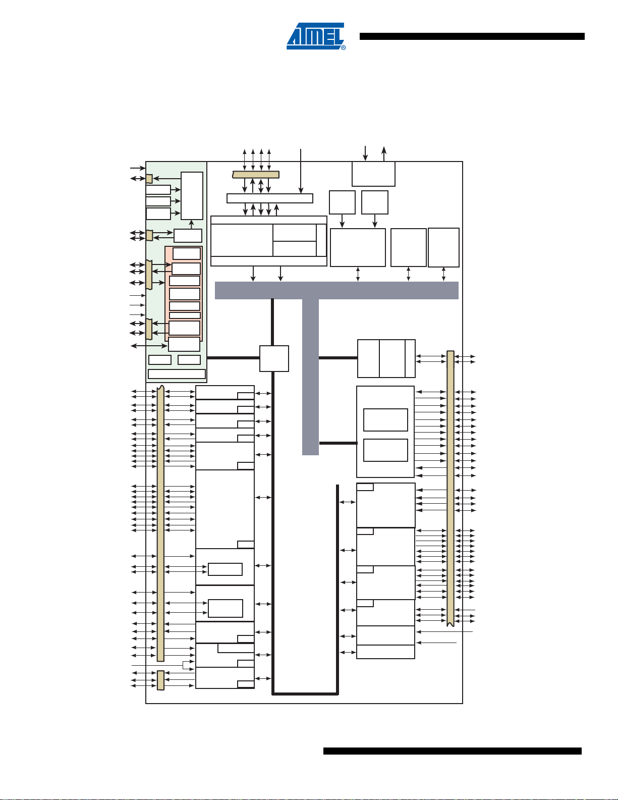
2. Block Diagram
PLLA
System C ontroller
WDT
RTT
Osc 32 kHz
SUPC
RSTC
8 GPBREG
3-20 MHz
Osc
POR
RTC
RC 32 kHz
SM
RC Osc
12/8/4 MHz
I/D
S
MPU
N
V
I
C
4-layer AHB Bus Matrix Fmax 120 MHz
ADC Ch.
PLLB
PMC
PIOA / PIOB / PIOC
PIO
External Bus
Interface
D[7:0]
PIODC[7:0]
A[0:23]
A21/NANDALE
A22/NANDCLE
NCS0
NCS1
NCS2
NCS3
NRD
NWE
NANDOE
NANDWE
NWAIT
High Speed MCI
DATRG
PDC
PDC
PDC
PDC
PDC
PDC
PDC
PDC
PDC
PDC
PDC
PDC
PDC
DAC0
DAC1
Timer Counter B
Timer Counter A
TC[3..5]
TC[0..2]
TIOA[3:5]
TIOB[3:5]
TCLK[3:5]
AD[0..14]
RXD1
TXD1
USART1
USART0
UART1
UART0
SCK1
RTS1
CTS1
DSR1
DTR1
RI1
DCD1
NAND Flash
Logic
TWCK0
TWD0
TWD1
URXD0
UTXD0
URXD1
UTXD1
RXD0
TXD0
SCK0
RTS0
CTS0
TWCK1
ADVREF
TIOB[0:2]
TCLK[0:2]
PWMH[0:3]
PWML[0:3]
PWMFI0
ADTRG
TIOA[0:2]
TST
PCK0-PCK2
XIN
NRST
VDDCORE
XOUT
RTCOUT0
RTCOUT1
XIN32
XOUT32
ERASE
VDDPLL
VDDIO
12-bit DAC
Temp. Sensor
PWM
12-bit ADC
TWI0
TWI1
SPI
SSC
PIO
Static Memory
Controller
Analog
Comparator
CRC Unit
Peripheral
Bridge
2668
Bytes
FIFO
USB 2.0
Full
Speed
Transceiver
NPCS0
PIODCCLK
PIODCEN1
PIODCEN2
NPCS1
NPCS2
NPCS3
MISO
MOSI
SPCK
MCDA[0..3]
MCCDA
MCCK
TF
TK
TD
RD
RK
RF
DDP
DDM
ADVREF
ROM
16 Kbytes
FLASH
1024 Kbytes
512 Kbytes
Flash
Unique
Identifier
User
Signature
TDI
TDO
TMS/SWDIO
TCK/SWCLK
JTAGSEL
Voltage
Regulator
VDDIN
VDDOUT
Cortex-M4 Processor
Fmax 120 MHz
In-Circuit Emulator
JTAG & Serial Wire
24-Bit
SysTick Counter
DSP
SRAM
128 Kbytes
Figure 2-1. SAM4S16, S8 Series 100-pin version Block Diagram
4
SAM4S Series [Preliminary]
11100B–ATARM–31-Jul-12
Page 5
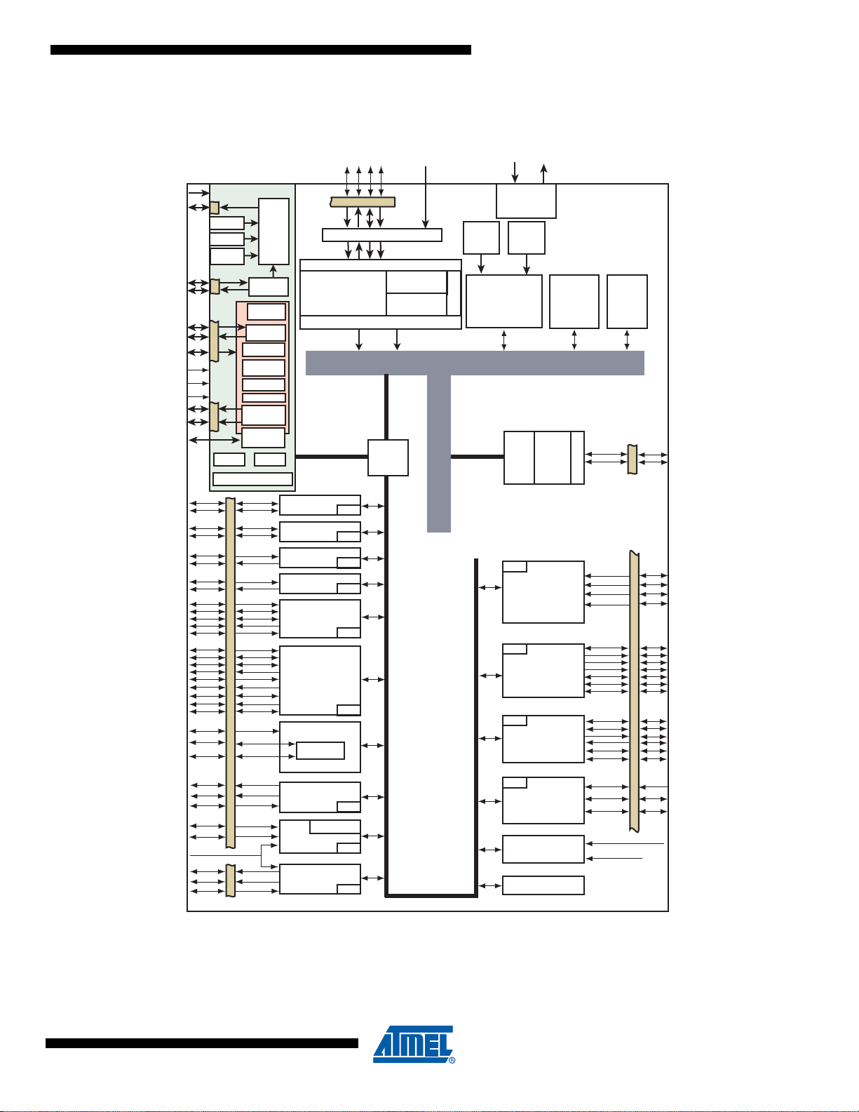
Figure 2-2. SAM4S16, S8 Series 64-pin version Block Diagram
PLLA
System C ontroller
WDT
RTT
Osc 32 kHz
SUPC
RSTC
8 GPBREG
3-20 MHz
Osc
POR
RTC
RC 32 kHz
SM
RC Osc
12/8/4 MHz
I/D
S
MPU
N
V
I
C
4-layer AHB Bus Matrix Fmax 120 MHz
ADC Ch.
PLLB
PMC
PIOA / PIOB
PIODC[7:0]
High Speed MCI
DATRG
PDC
PDC
PDC
PDC
PDC
PDC
PDC
PDC
PDC
PDC
PDC
PDC
PDC
DAC0
DAC1
Timer Counter A
TC[0..2]
AD[0..9]
RXD1
TXD1
USART1
USART0
UART1
UART0
SCK1
RTS1
CTS1
DSR1
DTR1
RI1
DCD1
TWCK0
TWD0
TWD1
URXD0
UTXD0
URXD1
UTXD1
RXD0
TXD0
SCK0
RTS0
CTS0
TWCK1
ADVREF
TIOB[0:2]
TCLK[0:2]
PWMH[0:3]
PWML[0:3]
PWMFI0
ADTRG
TIOA[0:2]
TST
PCK0-PCK2
XIN
NRST
VDDCORE
XOUT
RTCOUT0
RTCOUT1
XIN32
XOUT32
ERASE
VDDPLL
VDDIO
12-bit DAC
Temp. Sensor
PWM
12-bit ADC
TWI0
TWI1
SPI
SSC
PIO
Analog
Comparator
CRC Unit
Peripheral
Bridge
2668
Bytes
FIFO
USB 2.0
Full
Speed
Transceiver
NPCS0
PIODCCLK
PIODCEN1
PIODCEN2
NPCS1
NPCS2
NPCS3
MISO
MOSI
SPCK
MCDA[0..3]
MCCDA
MCCK
TF
TK
TD
RD
RK
RF
DDP
DDM
ADVREF
TDI
TDO
TMS/SWDIO
TCK/SWCLK
JTAGSEL
Voltage
Regulator
VDDIN
VDDOUT
Cortex-M4 Processor
Fmax 120 MHz
In-Circuit Emulator
JTAG & Serial Wire
24-Bit
SysTick Counter
PIO
PIO
DSP
ROM
16 Kbytes
FLASH
1024 Kbytes
512 Kbytes
Flash
Unique
Identifier
User
Signature
SRAM
128 Kbytes
SAM4S Series [Preliminary]
11100B–ATARM–31-Jul-12
5
Page 6
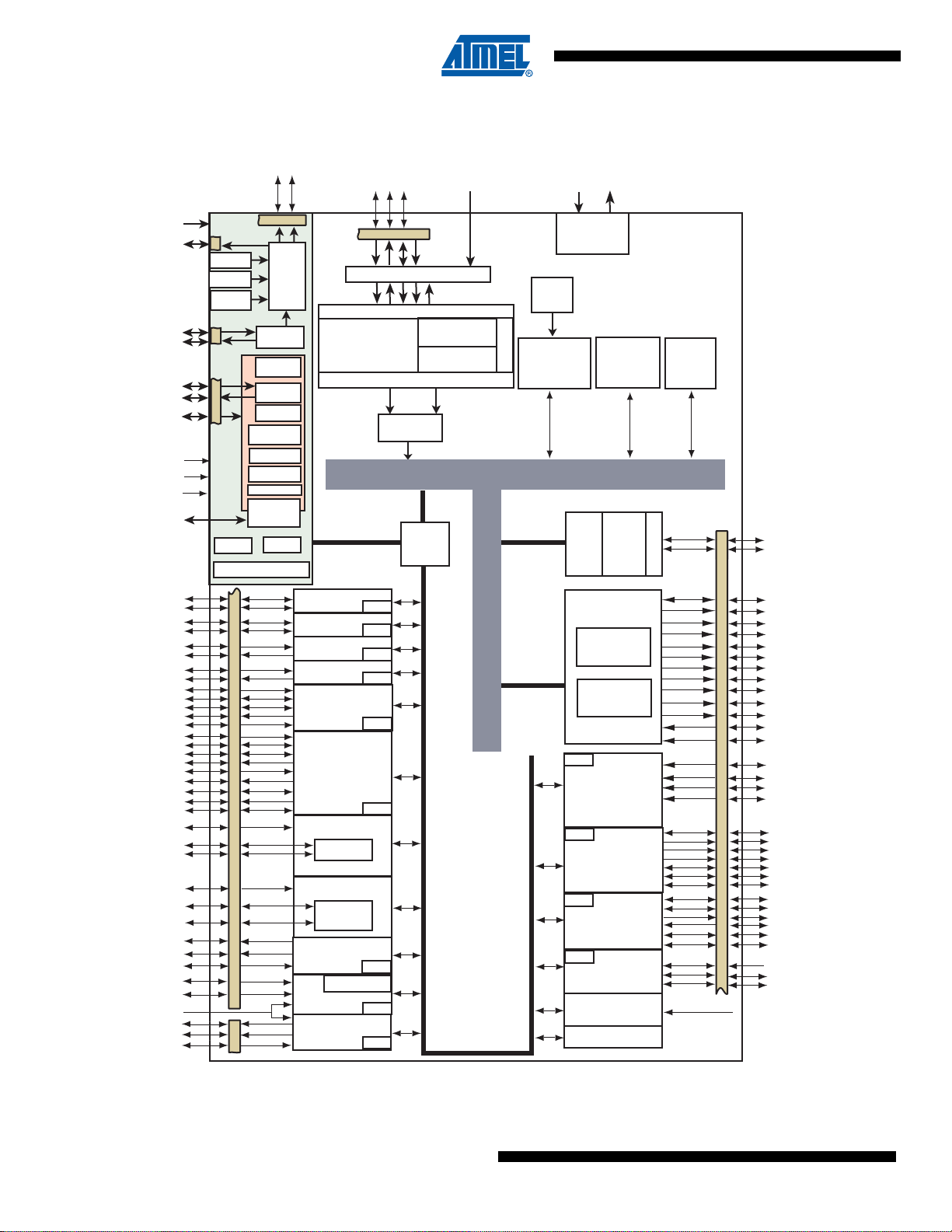
Figure 2-3. SAM4SD32, SD16, SA16 100-pin version Block Diagram
PLLA
TST
PCK0-PCK2
XIN
NRST
VDDCORE
XOUT
WDT
RTT
OSC 32k
XIN32
XOUT32
SUPC
RSTC
8 GPBREG
3-20 MHz
Osc.
POR
RTC
RC 32k
SM
RC
12/8/4 M
ERASE
TDI
TDO
TMS/SWDIO
TCK/SWCLK
JTAGSEL
I
D
Volt age
Regulator
VDDIN
VDDOUT
SPI
TC[0..2]
DAC
ADVREF
PDC
NPCS0
PIODCCLK
PIODCEN1
PIODCEN2
NPCS1
NPCS2
NPCS3
MISO
MOSI
SPCK
MCDA[0..3]
MCCDA
MCCK
TCLK[0:2]
Temp. Sensor
PDC
TWI0
PDC
TWD0
PWM
PDC
TF
TK
TD
RD
RK
RF
DDP
DDM
MPU
N
V
I
C
24-Bit
SysTick Counter
4-layer AHB Bus Matrix Fmax 120 MHz
TWI1
PDC
TWCK1
TWD1
PWMH[0:3]
PWML[0:3]
PWMFI0
PDC
UART0
UART1
URXD0
UTXD0
URXD1
UTXD1
SSC
Peripheral
Bridge
PDC
PIO
PDC
PDC
2668
Bytes
FIFO
USB 2.0
Full
Speed
VDDPLL
VDDIO
PDC
RXD0
TXD0
USART0
SCK0
RTS0
CTS0
Analog
Comparator
CRC Unit
ADC
Transceiver
PLLB
In-Circuit Emulator
JTAG & Serial Wire
Flash
Unique
Identifier
PMC
PIOA / PIOB / PIOC
ADTRG
Cortex-M4 Processor
Fmax 120 MHz
Timer Counter A
Timer Counter B
TWCK0
FLASH
2*1024 KBytes
2*512 KBytes
1024 KBytes
SRAM
160 KBytes
ROM
16 KBytes
RTCOUT1
RTCOUT0
DSP
CMCC
(2 KB cache)
PIO
External Bus
Interface
D[7:0]
PIODC[7:0]
A[0:23]
A21/NANDALE
A22/NANDCLE
NCS0
NCS1
NCS2
NCS3
NRD
NWE
NANDOE
NANDWE
NWAIT
High Speed MCI
PDC
DATRG
PDC
DAC0
DAC1
TC[3..5]
TIOA[3:5]
TIOB[3:5]
TIOA[0:2]
TIOB[0:2]
TCLK[3:5]
AD[0..14]
PDC
RXD1
TXD1
USART1
SCK1
RTS1
CTS1
DSR1
DTR1
RI1
DCD1
NAND Flash
Logic
Static Memory
Controller
ADC
DAC
Temp Sensor
ADVREF
6
SAM4S Series [Preliminary]
11100B–ATARM–31-Jul-12
Page 7
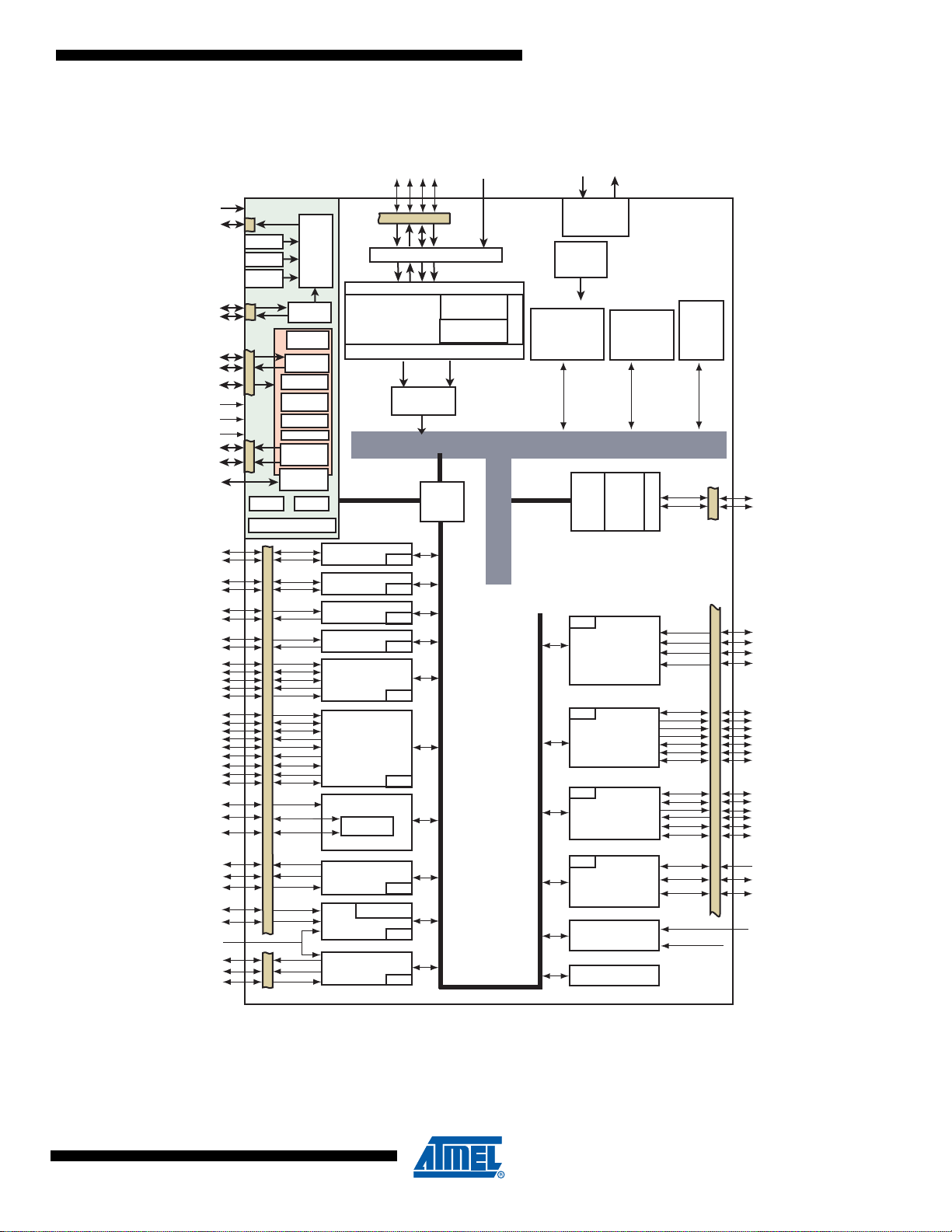
Figure 2-4. SAM4SD32, SD16, SA16 64-pin version Block Diagram
PLLA
System C ontroller
WDT
RTT
Osc 32 kHz
SUPC
RSTC
8 GPBREG
3-20 MHz
Osc
POR
RTC
RC 32 kHz
SM
RC Osc
12/8/4 MHz
MPU
N
V
I
C
4-layer AHB Bus Matrix Fmax 120 MHz
ADC Ch.
PLLB
PMC
PIOA / PIOB
PIODC[7:0
High Speed MCI
DATRG
PDC
PDC
PDC
PDC
PDC
PDC
PDC
PDC
PDC
PDC
PDC
PDC
PDC
DAC0
DAC1
Timer Counter A
TC[0..2]
AD[0..9]
RXD1
TXD1
USART1
USART0
UART1
UART0
SCK1
RTS1
CTS1
DSR1
DTR1
RI1
DCD1
TWCK0
TWD0
TWD1
URXD0
UTXD0
URXD1
UTXD1
RXD0
TXD0
SCK0
RTS0
CTS0
TWCK1
ADVREF
TIOB[0:2]
TCLK[0:2]
PWMH[0:3]
PWML[0:3]
PWMFI0
ADTRG
TIOA[0:2]
TST
PCK0-PCK2
XIN
NRST
VDDCORE
XOUT
RTCOUT0
RTCOUT1
XIN32
XOUT32
ERASE
VDDPLL
VDDIO
12-bit DAC
Temp. Sensor
PWM
12-bit ADC
TWI0
TWI1
SPI
SSC
PIO
Analog
Comparator
CRC Unit
Peripheral
Bridge
2668
Bytes
FIFO
USB 2.0
Full
Speed
Transceiver
NPCS0
PIODCCLK
PIODCEN
PIODCEN2
NPCS1
NPCS2
NPCS3
MISO
MOSI
SPCK
MCDA[0..3
MCCDA
MCCK
TF
TK
TD
RD
RK
RF
DDP
DDM
ADVREF
Flash
Unique
Identifier
TDI
TDO
TMS/SWDIO
TCK/SWCLK
JTAGSEL
Voltage
Regulator
VDDIN
VDDOUT
Cortex-M4 Processor
Fmax 120 MHz
In-Circuit Emulator
JTAG & Serial Wire
24-Bit
SysTick Counter
PIO
PIO
DSP
ROM
16 KBytes
I
D
FLASH
2*1024 KBytes
2*512 KBytes
1024 KBytes
SRAM
160 KBytes
CMCC
(2 KB cache)
SAM4S Series [Preliminary]
11100B–ATARM–31-Jul-12
7
Page 8
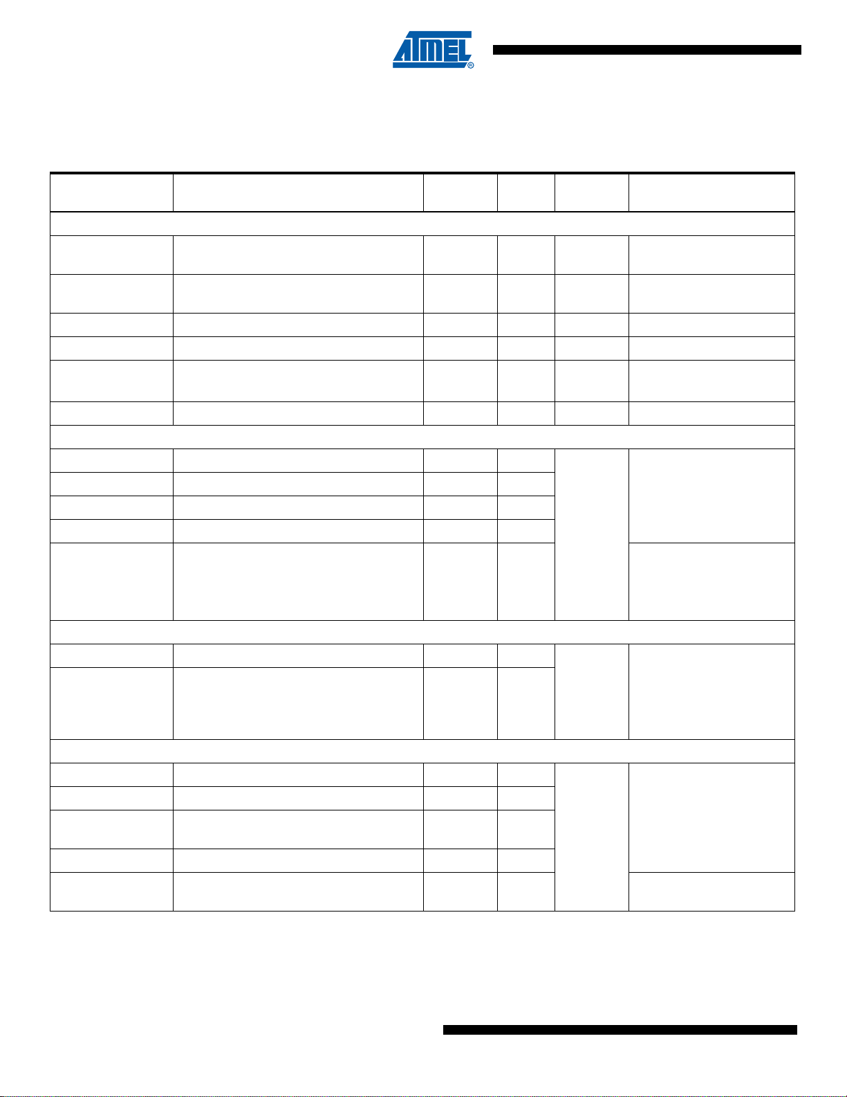
3. Signal Description
Table 3-1 gives details on signal names classified by peripheral.
Table 3-1. Signal Description List
Signal Name Function Type
Active
Level
Voltage
reference Comments
Power Supplies
VDDIO
VDDIN
Peripherals I/O Lines and USB transceiver
Power Supply
Voltage Regulator Input, ADC, DAC and
Analog Comparator Power Supply
Power 1.62V to 3.6V
Power 1.62V to 3.6V
VDDOUT Voltage Regulator Output Power 1.2V Output
VDDPLL Oscillator and PLL Power Supply Power 1.08 V to 1.32V
VDDCORE
Power the core, the embedded memories
and the peripherals
Power
1.08V to 1.32V
GND Ground Ground
Clocks, Oscillators and PLLs
XIN Main Oscillator Input Input
XOUT Main Oscillator Output Output
XIN32 Slow Clock Oscillator Input Input
XOUT32 Slow Clock Oscillator Output Output
VDDIO
Reset State:
- PIO Input
- Internal Pull-up disabled
- Schmitt Trigger enabled
Reset State:
PCK0 - PCK2 Programmable Clock Output Output
- PIO Input
- Internal Pull-up enabled
- Schmitt Trigger enabled
(4)
(1)
(1)
Real Time Clock
RTCOUT0 Programmable RTC waveform output Output
RTCOUT1 Programmable RTC waveform output Output
Serial Wire/JTAG Debug Port - SWJ-DP
TCK/SWCLK Test Clock/Serial Wire Clock Input
TDI Test Dat a In Input
TDO/TRACESWO
Test Data Out / Trace Asynchronous Data
Out
Output
TMS/SWDIO Test Mode Select /Serial Wire Input/Output Input / I/O
JTA G SEL JTA G Selection Input High
8
SAM4S Series [Preliminary]
VDDIO
VDDIO
Reset State:
- PIO Input
- Internal Pull-up enabled
- Schmitt Trigger enabled
Reset State:
- SWJ-DP Mode
- Internal pull-up disabled
- Schmitt Trigger enabled
Permanent Internal
pull-down
11100B–ATARM–31-Jul-12
(1)
(5)
(1)
Page 9
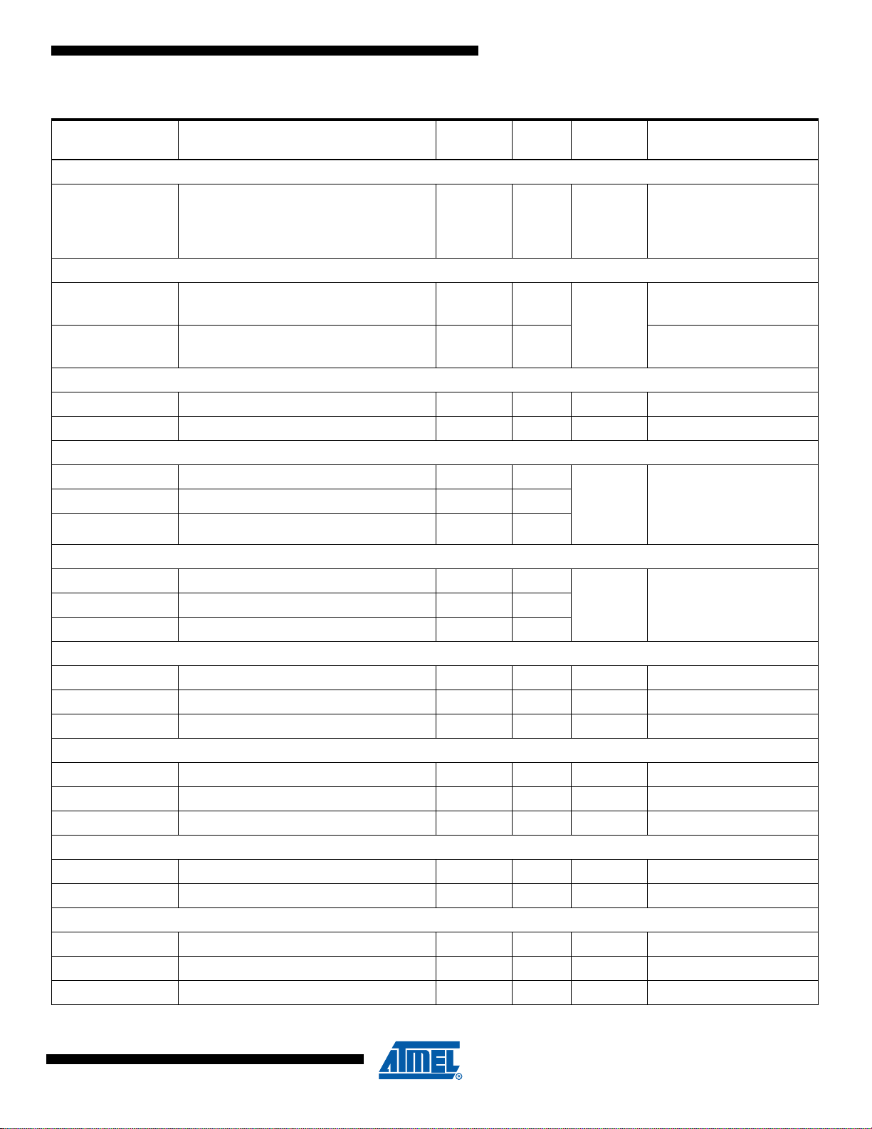
Table 3-1. Signal Description List (Continued)
SAM4S Series [Preliminary]
Active
Signal Name Function Type
Level
Flash Memory
ERASE
Flash and NVM Configuration Bits Erase
Command
Input High VDDIO
Reset/Test
NRST Synchronous Microcontroller Reset I/O Low
TST Test Select Input
Universal Asynchronous Receiver Transceiver - UARTx
URXDx UART Receive Data Input
UTXDx UART Transmit Data Output
PIO Controller - PIOA - PIOB - PIOC
PA0 - PA31 Parallel IO Controller A I/O
PB0 - PB14 Parallel IO Controller B I/O
PC0 - PC31 Parallel IO Controller C I/O
Voltage
reference Comments
Reset State:
- Erase Input
- Internal pull-down enabled
- Schmitt Trigger enabled
Permanent Internal
VDDIO
pull-up
Permanent Internal
pull-down
Reset State:
VDDIO
- PIO or System IOs
- Internal pull-up enabled
- Schmitt Trigger enabled
(1)
(2)
(1)
PIO Controller - Parallel Capture Mode
PIODC0-PIODC7 Parallel Capture Mode Data Input
PIODCEN1-2 Parallel Capture Mode Enable Input
External Bus Interface
D0 - D7 Data Bus I/O
A0 - A23 Address Bus Output
NWAIT External Wait Signal Input Low
Static Memory Controller - SMC
NCS0 - NCS3 Chip Select Lines Output Low
NRD Read Signal Output Low
NWE Write Enable Output Low
NAND Flash Logic
NANDOE NAND Flash Output Enable Output Low
NANDWE NAND Flash Write Enable Output Low
High Speed Multimedia Card Interface - HSMCI
MCCK Multimedia Card Clock I/O
MCCDA Multimedia Card Slot A Command I/O
MCDA0 - MCDA3 Multimedia Card Slot A Data I/O
VDDIOPIODCCLK Parallel Capture Mode Clock Input
11100B–ATARM–31-Jul-12
9
Page 10

Table 3-1. Signal Description List (Continued)
Signal Name Function Type
Universal Synchronous Asynchronous Receiver Transmitter USARTx
SCKx USARTx Serial Clock I/O
TXDx USARTx Transmit Data I/O
RXDx USARTx Receive Data Input
RTSx USARTx Request To Send Output
CTSx USARTx Clear To Send Input
DTR1 USART1 Data Terminal Ready I/O
DSR1 USART1 Data Set Ready Input
DCD1 USART1 Data Carrier Detect Output
RI1 USART1 Ring Indicator Input
Synchronous Serial Controller - SSC
TD SSC Transmit Data Output
RD SSC Receive Data Input
TK SSC Transmit Clock I/O
RK SSC Receive Clock I/O
TF SSC Transmit Frame Sync I/O
RF SSC Receive Frame Sync I/O
Timer/Counter - TC
Active
Level
Voltage
reference Comments
TCLKx TC Channel x External Clock Input Input
TIOAx TC Channel x I/O Line A I/O
TIOBx TC Channel x I/O Line B I/O
Pulse Width Modulation Controller- PWMC
PWMHx PWM Waveform Output High for channel x Output
PWMLx PWM Waveform Output Low for channel x Output
PWMFI0 PWM Fault Input Input
Serial Peripheral Interface - SPI
MISO Master In Slave Out I/O
MOSI Master Out Slave In I/O
SPCK SPI Serial Clock I/O
SPI_NPCS0 SPI Peripheral Chip Select 0 I/O Low
SPI_NPCS1 -
SPI_NPCS3
SPI Peripheral Chip Select Output Low
only output in
complementary mode
when dead time insertion
is enabled.
10
SAM4S Series [Preliminary]
11100B–ATARM–31-Jul-12
Page 11
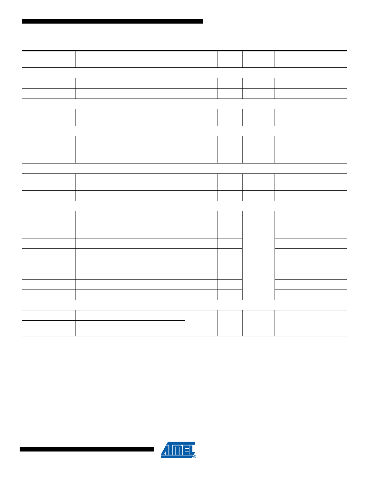
Table 3-1. Signal Description List (Continued)
SAM4S Series [Preliminary]
Active
Signal Name Function Type
Two-Wire Interface- TWI
TWDx TWIx Two-wire Serial Data I/O
TWCKx TWIx Two-wire Serial Clock I/O
Analog
ADVREF
AD0-AD14 Analog Inputs
ADTRG ADC Trigger Input VDDIO
DAC0 - DAC1 Analog output
DACTRG DAC Trigger Input VDDIO
PGMEN0PGMEN2
PGMM0-PGMM3 Programming Mode Input
ADC, DAC and Analog Comparator
Reference
12-bit Analog-to-Digital Converter - ADC
12-bit Digital-to-Analog Converter - DAC
Fast Flash Programming Interface - FFPI
Programming Enabling Input VDDIO
Analog
Analog,
Digital
Analog,
Digital
Level
Voltage
reference Comments
PGMD0-PGMD15 Programming Data I/O
PGMRDY Programming Ready Output High
PGMNV ALID Data Direction Output Low
PGMNOE Programming Read Input Low
PGMCK Programming Clock Input
PGMNCMD Programming Command Input Low
USB Full Speed Device
DDM USB Full Speed Data DDP USB Full Speed Data +
Note: 1. Schmitt Triggers can be disabled through PIO registers.
2. Some PIO lines are shared with System I/Os.
3. Refer to USB Section of the product Electrical Characteristics for information on Pull-down value in USB Mode.
4. See “Typical P owering Schematics” Section for restrictions on voltage range of Analog Cells.
5. TDO pin is set in input mode when the Cortex-M4 Core is not in debug mode. Thus the internal pull-up corresponding to this
PIO line must be enabled to avoid current consumption due to floating input
Analog,
Digital
VDDIO
VDDIO
Reset State:
- USB Mode
- Internal Pull-down
(3)
11100B–ATARM–31-Jul-12
11
Page 12
4. Package and Pinout
125
26
50
5175
76
100
SAM4S devices are pin-to-pin compatible with SAM3N, SAM3S product s in 64- and 100- pin versions, and AT91SAM7S legacy products in 64-pin versions.
4.1 SAM4SD32/SD16/SA16/S16/S8C Package and Pinout
4.1.1 100-Lead LQFP Package Outline
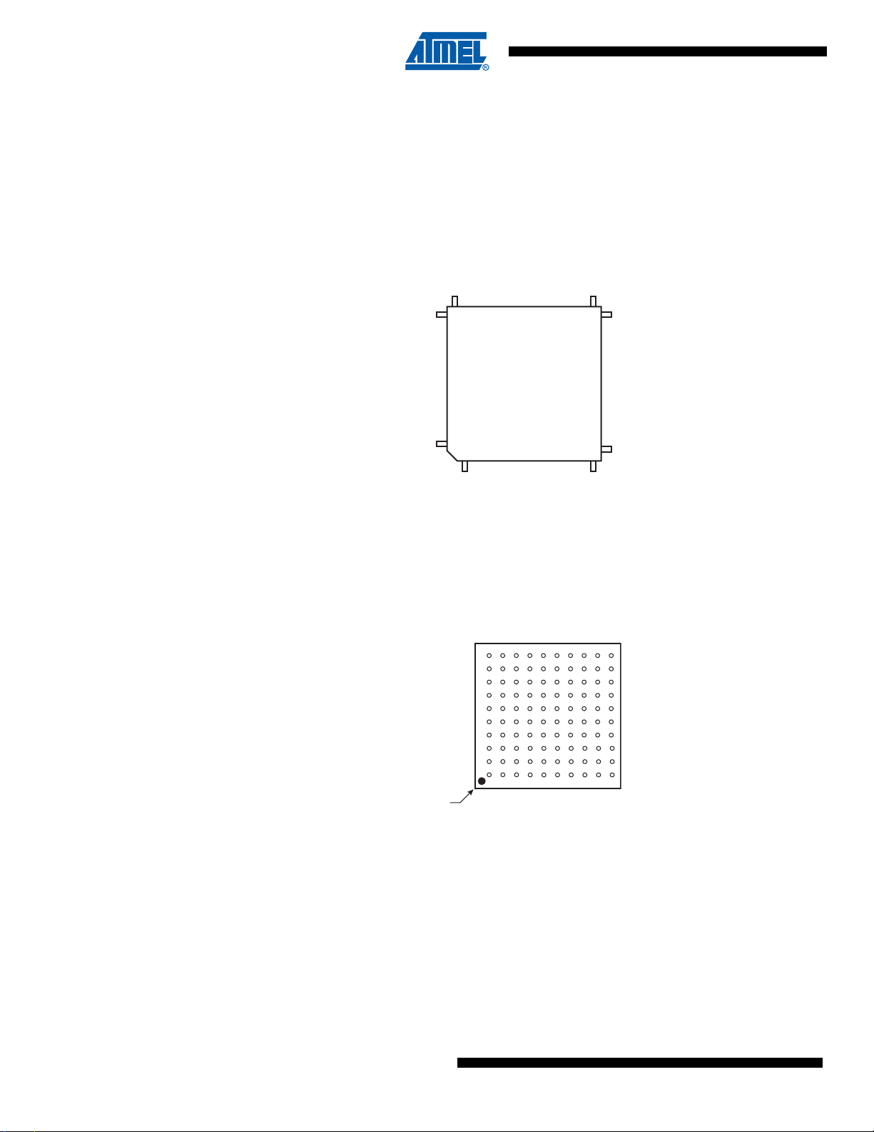
Figure 4-1. Orientation of the 100-lead LQFP Package
4.1.2 100-ball TFBGA Package Outline
The 100-Ball TFBGA package has a 0.8 mm ball pitch and respects Green Standards. Its
dimensions are 9 x 9 x 1.1 mm. Figure 4-2 shows the orientation of the 100-ball TFBGA
Package.
Figure 4-2. Orientation of the 100-ball TFBGA Package
TOP VIEW
10
9
8
7
6
5
4
3
2
1
BALL A1
ABCDEFGHJK
12
SAM4S Series [Preliminary]
11100B–ATARM–31-Jul-12
Page 13
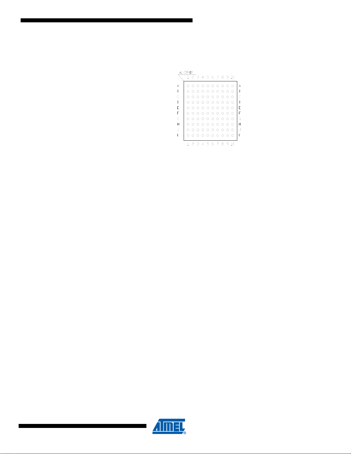
4.1.3 100-ball VFBGA Package Outline
Figure 4-3. Orientation of the 100-ball VFBGA Package
SAM4S Series [Preliminary]
11100B–ATARM–31-Jul-12
13
Page 14
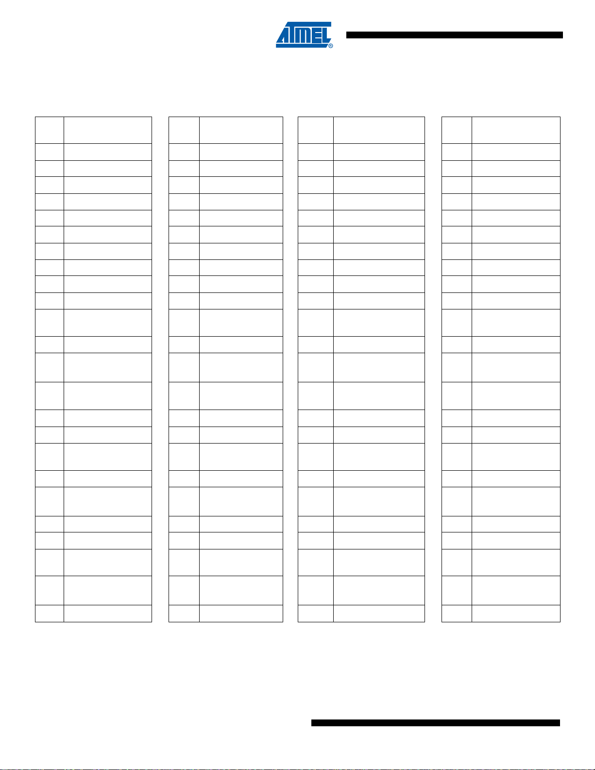
4.1.4 100-Lead LQFP Pinout
Table 4-1. SAM4SD32/SD16/SA16/S16/S8C 100-lead LQFP pinout
1 ADVREF 26 GND 51 TDI/PB4 76
2 GND 27 VDDIO 52 PA6/PGMNOE 77 JTAGSEL
3 PB0/AD4 28 PA16/PGMD4 53 PA5/PGMRDY 78 PC18
4 PC29/AD13 29 PC7 54 PC28 79 TMS/SWDIO/PB6
5 PB1/AD5 30 PA15/PGMD3 55 PA4/PGMNCMD 80 PC19
6 PC30/AD14 31 PA14/PGMD2 56 VDDCORE 81 PA31
7 PB2/AD6 32 PC6 57 PA27/PGMD15 82 PC20
8 PC31 33 PA13/PGMD1 58 PC8 83 TCK/SWCLK/PB7
9 PB3/AD7 34 PA24/PGMD12 59 PA28 84 PC21
10 VDDIN 35 PC5 60 NRST 85 VDDCORE
11 VDDOUT 36 VDDCORE 61 TST 86 PC22
12
13 PC26 38 PA25/PGMD13 63 PA29 88 DDM/PB10
14
15
16 VDDCORE 41 PA12/PGMD0 66 PA3 91 VDDIO
PA17/PGMD5/
AD0
PA18/PGMD6/
AD1
PA21/PGMD9/
AD8
37 PC4 62 PC9 87 ERASE/PB12
39 PA26/PGMD14 64 PA30 89 DDP/PB11
40 PC3 65 PC10 90 PC23
TDO/TRACESWO/
PB5
17 PC27 42 PA11/PGMM3 67 PA2/PGMEN2 92 PC24
18
19 PC15/AD11 44 PA10/PGMM2 69 VDDIO 94 PC25
20
21 PC13/AD10 46 PA9/PGMM1 71 PC14 96 PB8/XOUT
22 PA23/PGMD11 47 PC1 72 PA1/PGMEN1 97 PB9/PGMCK/XIN
23 PC12/AD12 48
24
25 PC0 50 VDDIO 75 PC17 100 VDDPLL
PA19/PGMD7/
AD2
PA22/PGMD10/
AD9
PA20/PGMD8/
AD3
43 PC2 68 PC11 93 PB13/DAC0
45 GND 70 GND 95 GND
49
PA8/XOUT32/
PGMM0
PA7/XIN32/
PGMNVALID
73 PC16 98 VDDIO
74 PA0/PGMEN0 99 PB14/DAC1
14
SAM4S Series [Preliminary]
11100B–ATARM–31-Jul-12
Page 15
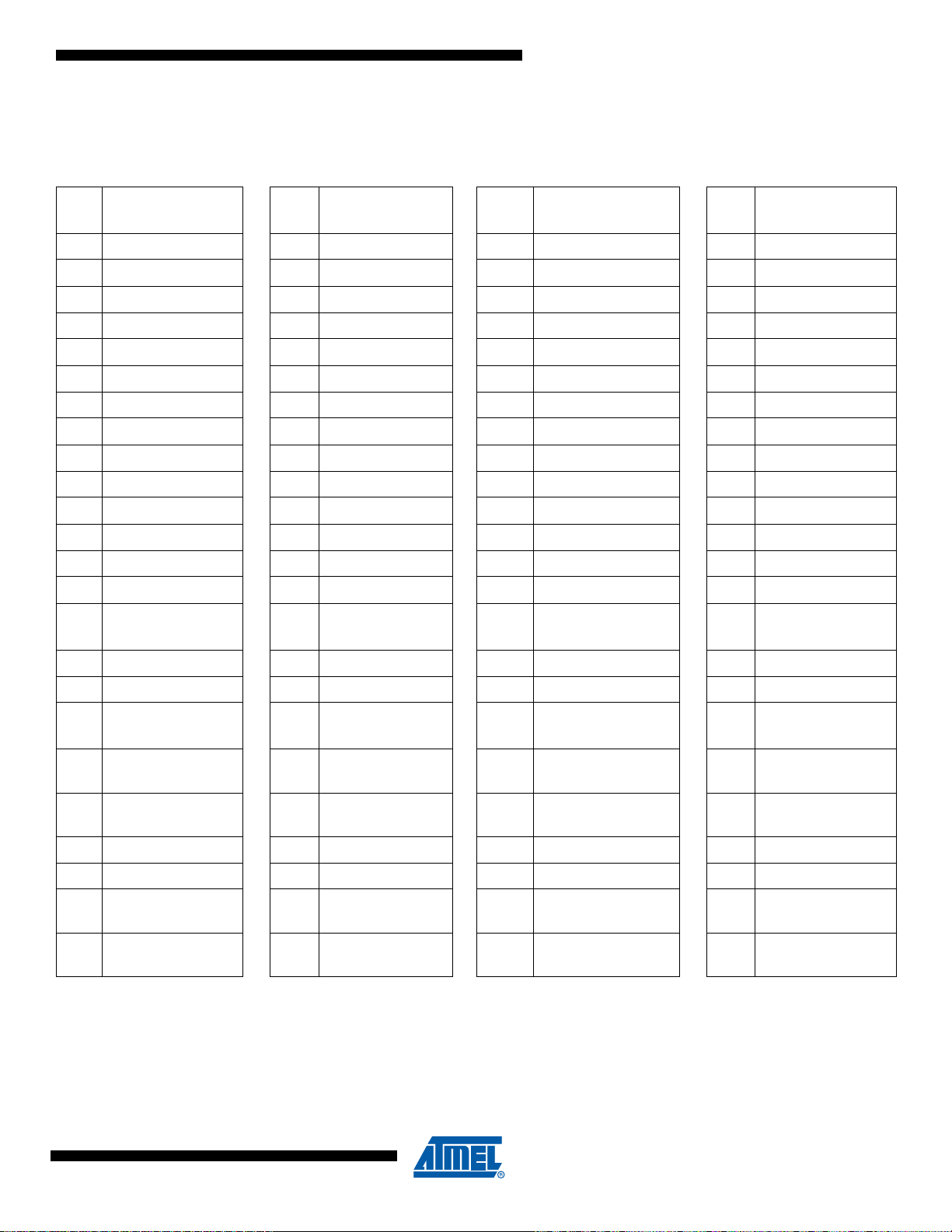
4.1.5 100-Ball TFBGA Pinout
Table 4-2. SAM4SD32/SD16/SA16/S16/S8 100-ball TFBGA pinout
SAM4S Series [Preliminary]
A1 PB1/AD5 C6 TCK/SWCLK/PB7 F1
A2 PC29 C7 PC16 F2 PC26 H7 PA11/PGMM3
A3 VDDIO C8 PA1/PGMEN1 F3 VDDOUT H8 PC1
A4 PB9/PGMCK/XIN C9 PC17 F4 GND H9 PA6/PGMNOE
A5 PB8/XOUT C10 PA0/PGMEN0 F5 VDDIO H10 TDI/PB4
A6 PB13/DAC0 D1 PB3/AD7 F6 PA27/PGMD15 J1 PC15/AD11
A7 DDP/PB11 D2 PB0/AD4 F7 PC8 J2 PC0
A8 DDM/PB10 D3 PC24 F8 PA28 J3 PA16/PGMD4
A9 TMS/SWDIO/PB6 D4 PC22 F9 TST J4 PC6
A10 JTAGSEL D5 GND F10 PC9 J5 PA24/PGMD12
B1 PC30 D6 GND G1 PA21/PGMD9/AD8 J6 PA25/PGMD13
B2 ADVREF D7 VDDCORE G2 PC27 J7 PA10/PGMM2
B3 GNDANA D8 PA2/PGMEN2 G3 PA15/PGMD3 J8 GND
B4 PB14/DAC1 D9 PC11 G4 VDDCORE J9 VDDCORE
B5 PC21 D10 PC14 G5 VDDCORE J10 VDDIO
B6 PC20 E1
PA17/PGMD5/
AD0
G6 PA26/PGMD14 K1
PA18/PGMD6/
AD1
H6 PC4
PA22/PGMD10/
AD9
B7 PA31 E2 PC31 G7 PA12/PGMD0 K2 PC13/AD10
B8 PC19 E3 VDDIN G8 PC28 K3 PC12/AD12
B9 PC18 E4 GND G9 PA4/PGMNCMD K4
B10
TDO/TRACESWO/
PB5
C1 PB2/AD6 E6 NRST H1
C2 VDDPLL E7 PA29/AD13 H2 PA23/PGMD11 K7 PC2
C3 PC25 E8 PA30/AD14 H3 PC7 K8 PA9/PGMM1
C4 PC23 E9 PC10 H4 PA14/PGMD2 K9
C5 ERASE/PB12 E10 PA3 H5 PA13/PGMD1 K10
E5 GND G10 PA5/PGMRDY K5 PC5
PA19/PGMD7/
AD2
K6 PC3
PA20/PGMD8/
AD3
PA8/XOUT32/
PGMM0
PA7/XIN32/
PGMNVALID
11100B–ATARM–31-Jul-12
15
Page 16
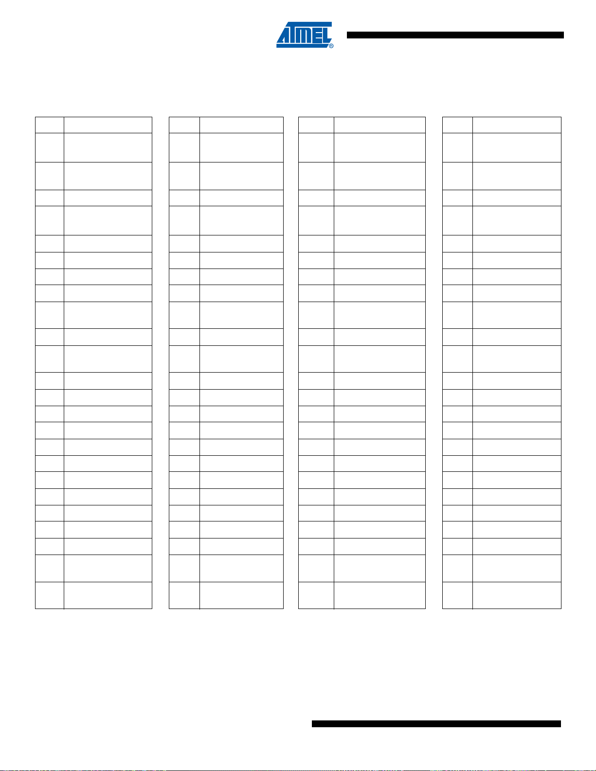
4.1.6 100-Ball VFBGA Pinout
Table 4-3. SAM4SD32/SD16/SA16/S16/S8 100-ball VFBGA pinout
A1 ADVREF C6 PC9 F1 VDDOUT H6 PA12/PGMD0
A2 VDDPLL C7 TMS/SWDIO/PB6 F2
A3 PB9/PGMCK/XIN C8 PA1/PGMEN1 F3
A4 PB8/XOUT C9 PA0/PGMEN0 F4 GND H9 PA6/PGMNOE
A5 JTAGSEL C10 PC16 F5 GND H10
A6 DDP/PB11 D1 PB1/AD5 F6 PC26 J1 PA20/AD3
A7 DDM/PB10 D2 PC30 F7 PA4/PGMNCMD J2 PC12/AD12
A8 PC20 D3 PC31 F8 PA28 J3 PA16/PGMD4
A9 PC19 D4 PC22 F9 TST J4 PC6
PA18/PGMD6/
AD1
PA17/PGMD5/
AD0
H7 PA9/PGMM1
H8 VDDCORE
PA5/PGMRDY
A10
B10 PC17 E5 GND G10 PA27 K5 PA26
TDO/TRACESWO/
PB5
B1 GNDANA D6 PA29/AD13 G1 PC15/AD11 J6 PA25
B2 PC25 D7 PA30/AD14 G2
B3 PB14/DAC1 D8 GND G3 PA21/AD8 J8 VDDCORE
B4 PB13/DAC0 D9 PC14 G4 PA15/PGMD3 J9 VDDCORE
B5 PC23 D10 PC11 G5 PC3 J10 TDI/PB4
B6 PC21 E1 VDDIN G6 PA10/PGMM2 K1 PA23
B7 TCK/SWCLK/PB7 E2 PB3/AD7 G7 PC1 K2 PC0
B8 PA31 E3 PB2/AD6 G8 PC28 K3 PC7
B9 PC18 E4 GND G9 NRST K4 PA13/PGMD1
C1 PB0/AD4 E6 GND H1 PC13/AD10 K6 PC2
C2 PC29 E7 VDDIO H2 PA22/AD9 K7 VDDIO
C3 PC24 E8 PC10 H3 PC27 K8 VDDIO
C4 ERASE/PB12 E9 PA2/PGMEN2 H4 PA14/PGMD2 K9
C5 VDDCORE E10 PA3 H5 PC4 K10
D5 PC5 F10 PC8 J5 PA24
PA19/PGMD7/
AD2
J7 PA11/PGMM3
PA8/XOUT32/
PGMM0
PA7/XIN32/
PGMNVALID
16
SAM4S Series [Preliminary]
11100B–ATARM–31-Jul-12
Page 17
SAM4S Series [Preliminary]
33
49
48
32
17
16
1
64
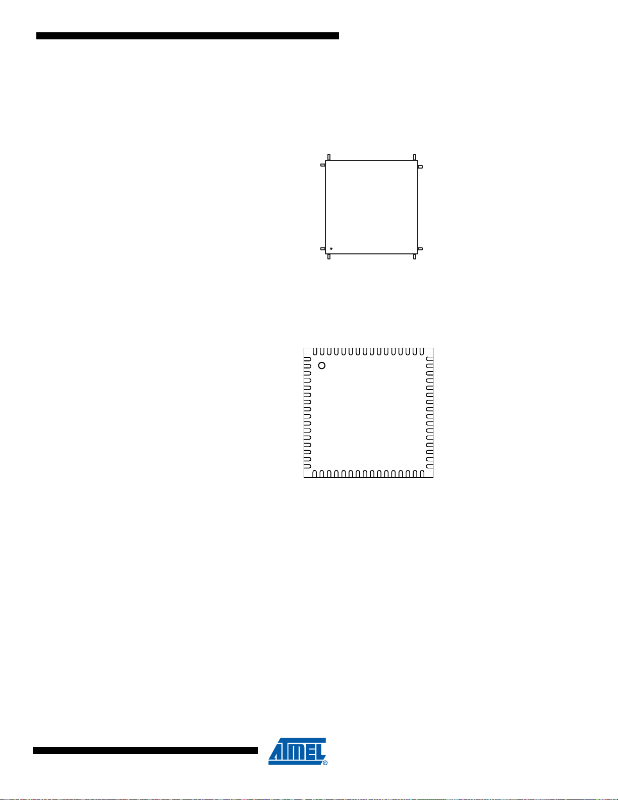
4.2 SAM4SD32/SD16/SA16/S16/S8 Package and Pinout
4.2.1 64-Lead LQFP Package Outl ine
Figure 4-4. Orientation of the 64-lead LQFP Package
4.2.2 64-lead QFN Package Outline
Figure 4-5. Orientation of the 64-lead QFN Package
16
4964
1
17
TOP VIEW
48
33
32
11100B–ATARM–31-Jul-12
17
Page 18
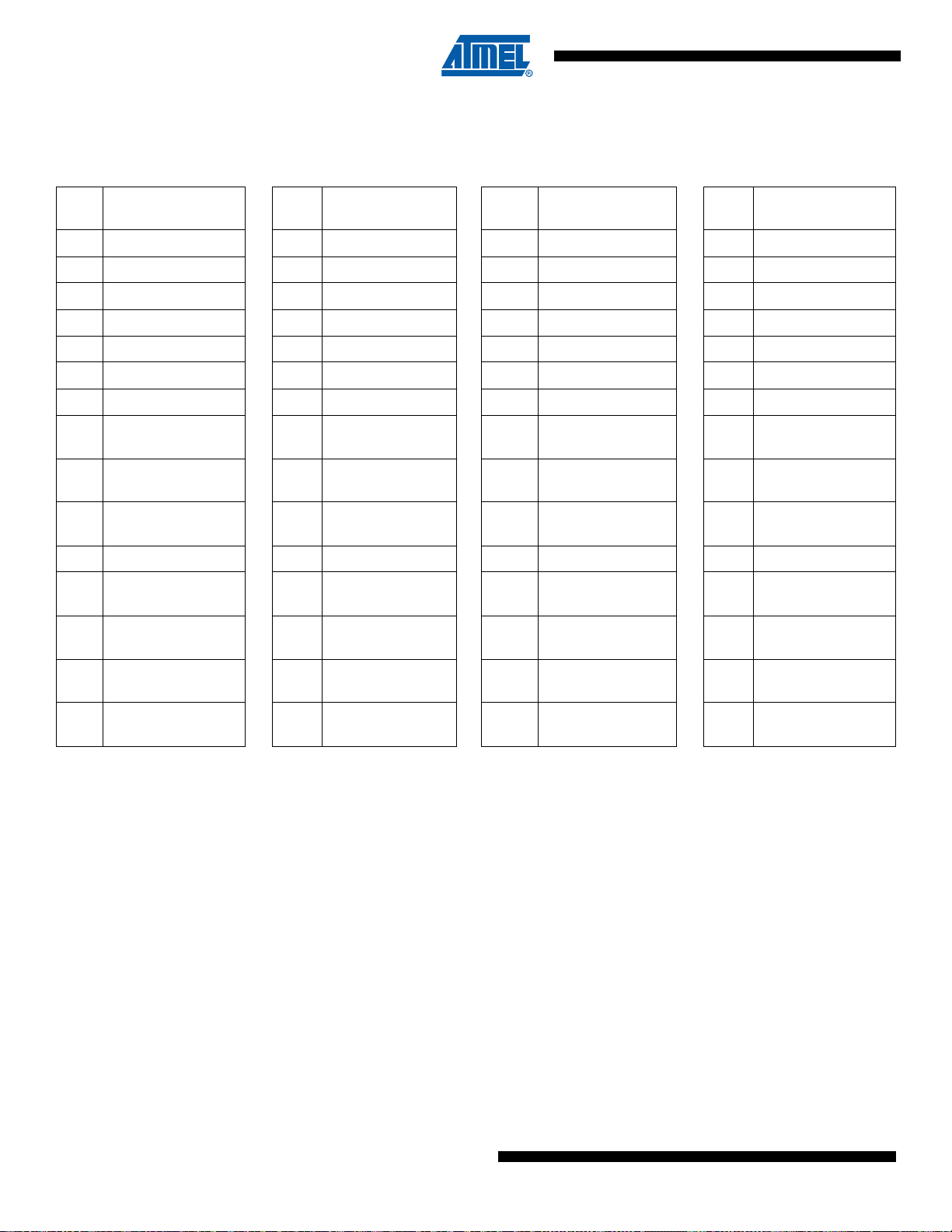
4.2.3 64-Lead LQFP and QFN Pinout
Table 4-4. 64-pin SAM4SD32/SD16/SA16/S16/S8 pinout
1 ADVREF 17 GND 33 TDI/PB4 49
2 GND 18 VDDIO 34 PA6/PGMNOE 50 JTAGSEL
3 PB0/AD4 19 PA16/PGMD4 35 PA5/PGMRDY 51 TMS/SWDIO/PB6
4 PB1/AD5 20 PA15/PGMD3 36 PA4/PGMNCMD 52 PA31
5 PB2/AD6 21 PA14/PGMD2 37 PA27/PGMD15 53 TCK/SWCLK/PB7
6 PB3/AD7 22 PA13/PGMD1 38 PA28 54 VDDCORE
7 VDDIN 23 PA24/PGMD12 39 NRST 55 ERASE/PB12
8 VDDOUT 24 VDDCORE 40 TST 56 DDM/PB10
9
10
11
12 VDDCORE 28 PA11/PGMM3 44 PA2/PGMEN2 60 GND
13
14
PA17/PGMD5/
AD0
PA18/PGMD6/
AD1
PA21/PGMD9/
AD8
PA19/PGMD7/
AD2
PA22/PGMD10/
AD9
25 PA25/PGMD13 41 PA29 57 DDP/PB11
26 PA26/PGMD14 42 PA30 58 VDDIO
27 PA12/PGMD0 43 PA3 59 PB13/DAC0
29 PA10/PGMM2 45 VDDIO 61 XOUT/PB8
30 PA9/PGMM1 46 GND 62 XIN/PGMCK/PB9
TDO/TRACESWO/
PB5
15 PA23/PGMD11 31
16
Note: The bottom pad of the QFN package must be connected to ground.
PA20/PGMD8/
AD3
32
PA8/XOUT32/
PGMM0
PA7/XIN32/
PGMNVALID
47 PA1/PGMEN1 63 PB14/DAC1
48 PA0/PGMEN0 64 VDDPLL
18
SAM4S Series [Preliminary]
11100B–ATARM–31-Jul-12
Page 19

5. Power Considerations
5.1 Po wer Supplies
The SAM4S has several types of power supply pins:
• VDDCORE pins: Power the core, the embedded memories and the peripherals. Voltage
ranges from 1.08V to 1.32V.
• VDDIO pins: Powe r the Peripherals I/ O lines (Input/ Output Buffers), USB tra nsceiv er, Bac kup
part, 32 kHz crystal oscillator and oscillator pads. Voltage ranges from 1.62V to 3.6V.
• VDDIN pin: Voltage Regulator Input, ADC, DAC and Analog Comparator Power Supply.
Voltage ranges from 1.62V to 3.6V.
• VDDPLL pin: Powers the PLLA, PLLB, the Fast RC and the 3 to 20 MHz oscillator. Voltage
ranges from 1.08V to 1.32V.
5.2 Voltage Regulator
The SAM4S embeds a voltage regulator that is managed by the Supply Controller.
This internal regulator is designed to supply the internal cor e of SAM4S It fe atures two o perat ing
modes:
SAM4S Series [Preliminary]
• In Normal mode, the voltage regulator consumes less than 500 µA static current and draws
80 mA of output current. Internal adaptive biasing adjusts the regulator quiescent current
depending on the required load current. In Wait Mode quiescent current is only 5 µA.
• In Backup mod e, the v oltage r egulator consumes less t han 1µA while its output (VDDOUT) is
driven internally to GND. The default output voltage is 1.20V and the start-up time to reach
Normal mode is less than 300 µs.
For adequate input and output power supply d ecoupling/bypassing , refer to the “ Voltage Regulator” section in the “Electrical Characteristics” section of the datasheet.
5.3 Typical Powering Schematics
The SAM4S supports a 1.62V-3.6V single supply mode. The internal regulator input is connected to the source and its output feeds VDDCORE. Figure 5-1 below shows the power
schematics.
As VDDIN powers the voltage regulator, the ADC, DAC and the analog comparator, when the
user does not want to use the embedded voltage regulator, it can be disabled by software via
the SUPC (note that this is different from Backup mode).
11100B–ATARM–31-Jul-12
19
Page 20
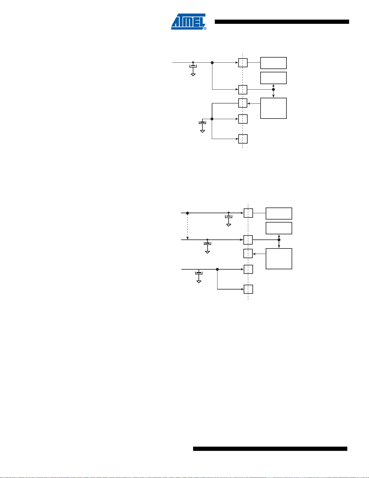
Figure 5-1. Single Supply
Main Supply
(1.62V-3.6V)
ADC, DAC
Analog Comp.
USB
Transceivers.
VDDIN
Voltage
Regulator
VDDOUT
VDDCORE
VDDIO
VDDPLL
Note: Restrictions
For USB, VDDIO needs to be greater than 3.0V.
For ADC, VDDIN needs to be greater than 2.0V.
For DAC, VDDIN needs to be greater than 2.4V.
Figure 5-2. Core Externally Supplied
Main Supply
(1.62V-3.6V)
Can be the
same supply
ADC, DAC, Analog
Comparator Supply
(2.0V-3.6V)
VDDCORE Supply
(1.08V-1.32V)
VDDIO
VDDIN
VDDOUT
VDDCORE
USB
Transceivers.
ADC, DAC
Analog Comp.
Voltage
Regulator
20
Note: Restrictions
For USB, VDDIO needs to be greater than 3.0V.
For ADC, VDDIN needs to be greater than 2.0V.
For DAC, VDDIN needs to be greater than 2.4V.
Figure 5-3 below provides an example of the powering scheme when using a backu p battery.
Since the PIO state is preserved when in backup mode, any free PIO line can be used to switch
off the external regulator by driving the PIO line at low level (PIO is input, pull-up enabled after
backup reset). External wake-up of the system can be from a push button or any signal. See
Section 5.6 “Wake-up Sources” for further details.
SAM4S Series [Preliminary]
VDDPLL
11100B–ATARM–31-Jul-12
Page 21
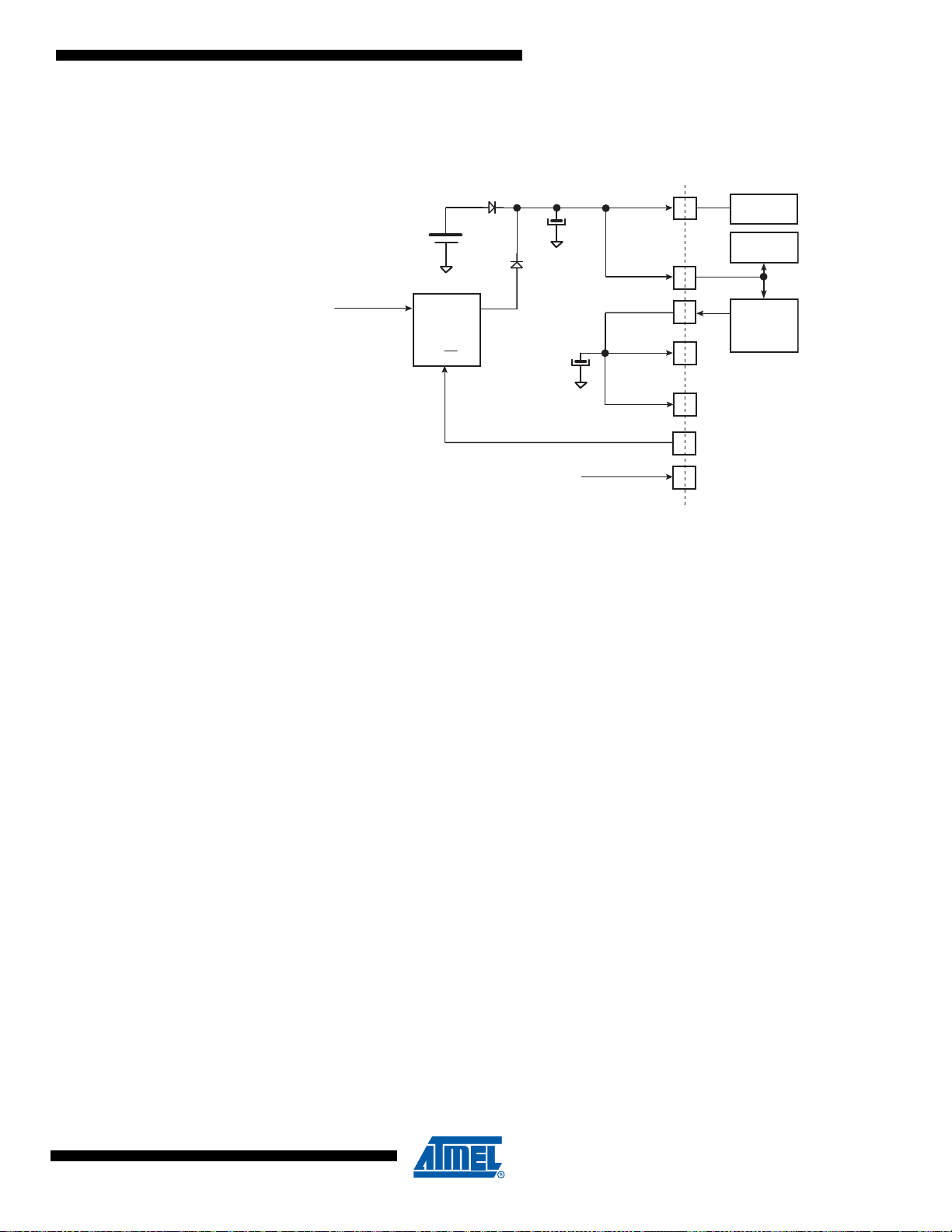
Figure 5-3. Backup Battery
ADC, DAC
Analog Comp.
USB
Transceivers.
VDDIN
Voltage
Regulator
3.3V
LDO
Backup
Battery
+
-
ON/OFF
IN
OUT
VDDOUT
Main Supply
VDDCORE
ADC, DAC, Analog
Comparator Supply
(2.0V-3.6V)
VDDIO
VDDPLL
PIOx (Output)
WAKEUPx
External wakeup signal
Note: The two diodes provide a “switchover circuit” (for illustration purpose)
between the backup battery and the main supply when the system is put in
backup mode.
SAM4S Series [Preliminary]
5.4 Active Mode
5.5 Low-power Modes
5.5.1 Backup Mode
Active mode is the normal running mode with the core clock running from the fast RC oscillator,
the main crystal oscillator or the PLLA. The power management controller can be used to adapt
the frequency and to disable the peripheral clocks.
The various low-power modes of the SAM4S are described below:
The purpose of backup mode is to achieve the lowest power consumption possible in a system
which is performing periodic wake-ups to perform tasks but not requiring fast startup time. Total
current consumption is 1 µA typical (VDDIO = 1.8 V to 25°).
The Supply Controller, zero-power power-on reset, RTT, RTC, Backup registers and 32 kHz
oscillator (RC or crystal oscillator selected by software in the Supply Controller) are running. The
regulator and the core supply are off.
Backup mode is based on the Cortex-M4 deep sleep mode with the voltage regula tor disabled.
The SAM4S can be awakened f rom th is m o de through WUP0-15 pins, the su pp ly m o nit or ( SM) ,
the RTT or RTC wake-up event.
Backup mode is entered by writing the Supply Controller Control Register (SUPC_CR) with the
VROFF bit at 1 (A key is needed to write t he VR OF F bi t, plea se ref er t o Supp ly Contr oller SUPC
section of the product datasheet) and with the SLEEPDEEP bit in the Cortex-M4 System Control
Register set to 1. (See the Power management description in The ARM Cortex-M4 Processor
section of the product datasheet).
11100B–ATARM–31-Jul-12
21
Page 22

5.5.2 Wait Mode
Entering Backup mode:
• Set the SLEEPDEEP bit of Cortex_M4 to 1
• Set the VR OFF bit of SUPC_CR to 1
Exit from Backup mode happens if one of the following enable wake up events occurs:
• WKUPEN0-15 pins (level transition, configurable debouncing)
• Supply Monitor alarm
•RTC alarm
• RTT alarm
The purpose of the wait mode is to achieve ve ry low power consumption while maintainin g the
whole device in a powered state for a startup time of less than 10 µs. Current Consumption in
Wait mode is typically 32 µA (total current consumption) if the internal voltage regulator is used.
In this mode, the clocks of the core, peripherals and memories are stopped. However, the core,
peripherals and memories power supplies are still powered. From this mode, a fast start up is
available.
This mode is entered by setting WAITMODE bit to 1 (in PMC clock generator Main Oscillator
register) with LPM = 1 (Low Power Mode bit in PMC_FSMR) and with FLPM = 00 or FLPM=01
(Flash Low Power Mode bits in PMC_FSMR).
The Cortex-M4 is able to handle external events or internal events in order to wake-up the core.
This is done by configuring the external lines WUP0-15 as fast startup wake-up pins (refer to
Section 5.7 “Fast Startup”). RTC or RTT Alarm and USB wake-up events can be used to wake
up the CPU.
Entering Wait Mode:
• Select the 4/8/12 MHz fast RC oscillator as Main Clock
• Set the LPM bit in the PMC Fast Startup Mode Register (PMC_FSMR)
• Set the FLPM bitfield in the PMC Fast Startup Mode Register (PMC_FSMR)
• Set Flash Wait State at 0.
• Set the WAITMODE bit = 1 in PMC Main Oscillator Register (CKGR_MOR)
• Wait for Master Clock Ready MCKRDY = 1 in the PMC Status Register (PMC_SR)
Note: Internal Main clock resynchronization cycles are necessary between the writing of MOSCRCEN
bit and the effective entry in Wait mode. Depending on the user application, waiting for
MOSCRCEN bit to be cleared is recommended to ensure that the core will not execute undesired
instructions.
Depending on Flash Low Power Mode (FLPM) value, the Flash will enter in three different
modes:
• FLPM[00] in Standby mode
• FLPM[01] in Deep Power Down mode
• FLPM[10] in Idle mode.
Following the Flash mode selection, the consumption in wait mode will decrease. In Deep Power
22
Down mode the recovery time of the Flash in Standby mode will be less than the power up
delay.
SAM4S Series [Preliminary]
11100B–ATARM–31-Jul-12
Page 23

SAM4S Series [Preliminary]
5.5.3 Sleep Mode
The purpose of sleep mode is to optimize power consumption of the device versus response
time. In this mode, only the core clock is stopped. The peripheral clocks can be enabled. The
current consumption in this mode is application dependent.
This mode is entered via Wait for Interrupt (WFI) instructions with LPM = 0 in PMC_FSMR.
The processor can be awakened from an interrupt if WFI instruction of the Cortex-M4 is used.
5.5.4 Low Power Mode Summary Table
The modes detailed above are the main low-power modes. Each part can be set to on or off separately and wake up sources can be individually configured. Table 5-1 below shows a summary
of the configurations of the low-power modes.
Table 5-1. Low-power Mode Configuration Summary
SUPC,
32 kHz Osc,
RTC, RTT
Backup
Registers,
POR
(Backup
Mode
Backup
Mode
Wait
Mode
w/Flash
in
Standby
mode
Wait
Mode
w/Flash
in Deep
Power
Down
mode
Sleep
Mode
Region) Regulator
ON OFF
ON ON
ON ON
ON ON
Notes: 1. The external loads on PIOs are not taken into account in the calculation.
2. Supply Monitor current consumption is not included.
3. When considering wake-up time, the time required to start the PLL is not taken into account. Once started, the device works
with the 4/8/12 MHz fast RC oscillator. The user has to add the PLL start-up time if it is needed in the system. The wake-up
time is defined as the time taken for wake up until the first instruction is fetched.
4. Total consumption 1 µA typ to 1.8V on VDDIO to 25°C.
5. 20.4 µA on VDDCORE, 32.2 µA for total current consumption.
6. Depends on MCK frequency.
7. Depends on MCK frequency. In this mode, the core is supplied but some peripherals can be clocked.
Core
Memory
Peripherals Mode Entry
OFF
(Not powered)
Powered
(Not clocked)
Powered
(Not clocked)
Powered
(Not clocked)
VROFF bit = 1
+SLEEPDEEP
bit = 1
WAITMODE bit
=1
+SLEEPDEEP
bit = 0
+LPM bit = 1
FLPM0 bit = 0
FLPM1 bit = 0
WAITMODE bit
=1
+SLEEPDEEP
bit = 0
+LPM bit = 1
FLPM0 bit = 0
FLPM1 bit = 1
WFI
(6)
+SLEEPDEEP
bit = 0
+LPM bit = 0
Potential Wake Up
Sources
WUP0-15 pins
SM alarm
RTC alarm
RTT alarm
Any Event from:
Fast startup through
WUP0-15 pins
RTC alarm
RTT alarm
USB wake-up
Any Event from:
Fast startup through
WUP0-15 pins
RTC alarm
RTT alarm
USB wake-up
Entry mode =WFI
Interrupt Only;
Any Enabled
Interrupt
Core at
Wake Up
Reset
Clocked
back
Clocked
back
Clocked
back
PIO State
while in Low
Power Mode
Previous
state saved
Previous
state saved
Previous
state saved
Previous
state saved
PIO State
at Wake Up
PIOA &
PIOB &
PIOC
Inputs with
pull ups
Unchanged 32.2 µA
Unchanged 27.6 µA < 10µs
Unchanged
Consumption
(1) (2)
1 µA typ
(7) (7)
Wake-up
Time
(4)
300 ms
(5)
< 10 µs
(3)
11100B–ATARM–31-Jul-12
23
Page 24
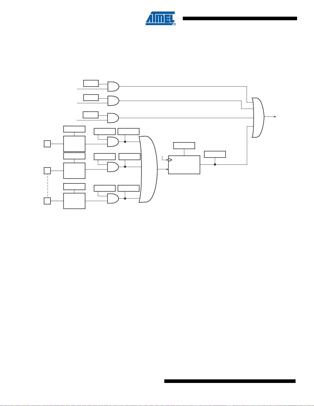
5.6 Wake-up Sour ces
WKUP15
WKUPEN15
WKUPT15
WKUPEN1
WKUPEN0
Debouncer
SLCK
WKUPDBC
WKUPS
RTCEN
rtc_alarm
SMEN
sm_out
Core
Supply
Restart
WKUPIS0
WKUPIS1
WKUPIS15
Falling/Rising
Edge
Detector
WKUPT0
Falling/Rising
Edge
Detector
WKUPT1
Falling/Rising
Edge
Detector
WKUP0
WKUP1
RTTEN
rtt_alarm
The wake-up events allow the device to exit the backup mode. When a wake-up event is
detected, the Supply Controller performs a sequence which automatically reenables the core
power supply and the SRAM power supply, if they are not already enabled.
Figure 5-4. Wake-up Source
24
SAM4S Series [Preliminary]
11100B–ATARM–31-Jul-12
Page 25
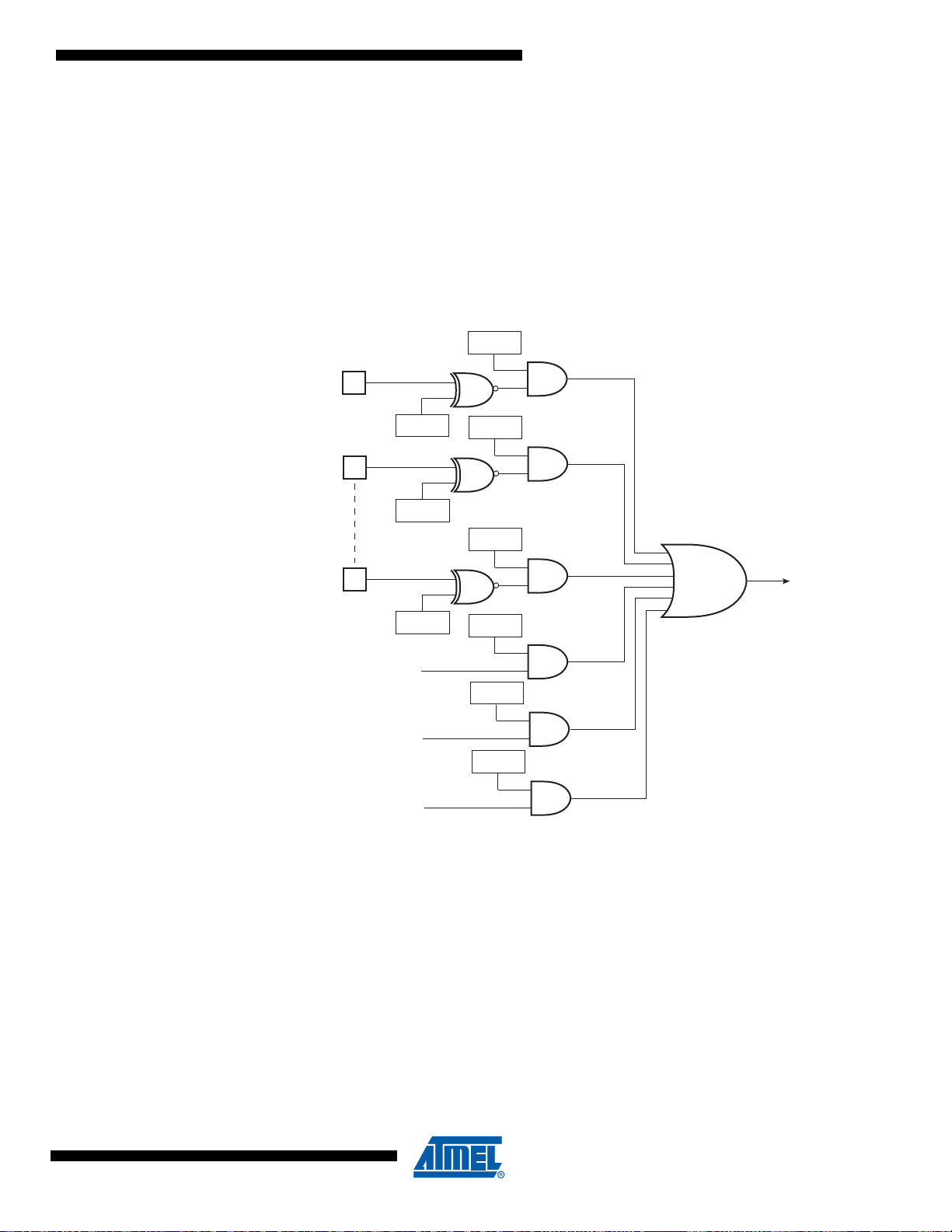
5.7 Fast Startup
SAM4S Series [Preliminary]
The SAM4S allows the processor to restart in a few microseconds while the processor is in wait
mode or in sleep mode. A fast start up can occur upon detection of a low level on one of the 19
wake-up inputs (WKUP0 to 15 + SM + RTC + RTT).
The fast restart circuitry, as shown in Figure 5-5, is fully asynchronous and provides a fast startup signal to the Power Management Controller. As soon as the fast start-up signal is asserted,
the PMC automatically restarts the embedded 4/8/12 MHz Fast RC oscillator, switches the master clock on this 4 MHz clock and reenables the processor clock.
Figure 5-5. Fast Start-Up Sources
FSTT0
WKUP0
WKUP1
WKUP15
FSTP0
FSTP1
FSTP15
RTT Alarm
RTC Alarm
USB Alarm
FSTT1
FSTT15
fast_restart
RTTAL
RTCAL
USBAL
11100B–ATARM–31-Jul-12
25
Page 26
6. Input/Output Lines
The SAM4S has several kinds of input/o utput (I/O) lines such as general pur pose I/Os (GPIO)
and system I/Os. GPIOs can have alternate functionality due to multiplexing capabilities of the
PIO controllers. The same PIO line can be used whether in I/O mode or by the multiplexed
peripheral. System I/Os include pins such as test pins, oscillators, erase or analog inputs.
6.1 General Purpose I/O Lines
GPIO Lines are managed by PIO Controllers. All I/Os have several input or output modes such
as pull-up or pull-down, input Schmitt triggers, multi-drive (open-drain), glitch filters, debouncing
or input change interrupt. Programming of these modes is performed independently for each I/O
line through the PIO controller user inte rface. F or mo re det ails, refe r to the p roduct “ PIO Contr oller” section.
The input/output buffers of the PIO lines are supplied through VDDIO power supply rail.
The SAM4S embeds high speed pads able to handle up to 7 0 MHz for HSMCI ( MCK/2), 7 0 MHz
for SPI clock lines and 46 MHz on other lines. See the “AC Characteristics” sub-section of the
product Electrical Characteristics. Typical pull-up and pull-down value is 100 kΩ for all I/Os.
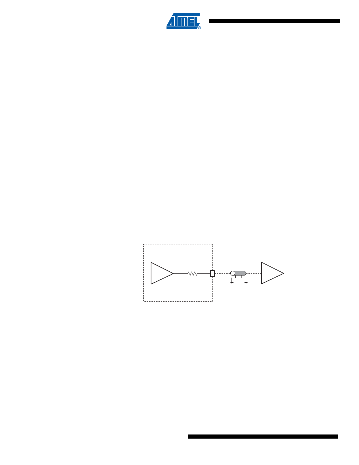
Each I/O line also embeds an ODT (On-Die Termination), (see Figure 6-1 below). It consists of
an internal series resistor termination scheme for impedance matching between the driver output (SAM4S) and the PCB trace impedance preventing signal reflection. The series resistor
helps to reduce IOs switching current (di/dt) thereby reducing in turn, EMI. It also decreases
overshoot and undershoot (ringing) due to inductance of interconnect between devices or
between boards. In conclusion ODT helps diminish signal integrity issues.
Figure 6-1. On-Die Termination
6.2 System I/O Lines
System I/O lines are pins used by oscillators, test mode, reset and JTAG to name but a few.
Described below in Table 6-1are the SAM4S system I/O lines shared with PIO lines.
These pins are software configurable as general purpose I/O or system pins. At startup the
default function of these pins is always used.
SAM4 Driver with
Zout ~ 10 Ohms
Z0 ~ Zout + Rodt
ODT
36 Ohms Typ.
Rodt
Receiver
PCB T race
Z0 ~ 50 Ohms
26
SAM4S Series [Preliminary]
11100B–ATARM–31-Jul-12
Page 27
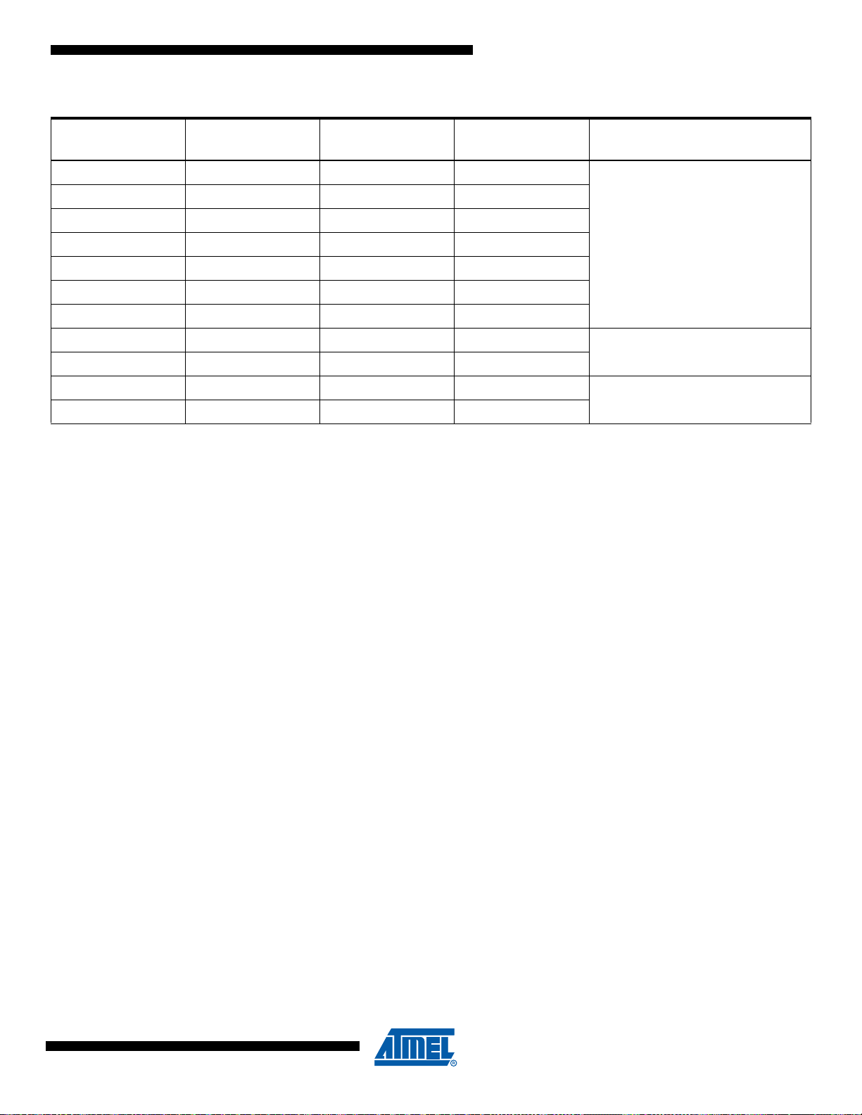
Table 6-1. System I/O Configuration Pin List.
SAM4S Series [Preliminary]
SYSTEM_IO
bit number
12 ERASE PB12 Low Level at startup
10 DDM PB10 11 DDP PB11 -
7 TCK/SWCLK PB7 6 TMS/SWDIO PB6 5 TDO/TRACESWO PB5 4 TDI PB4 -
- PA7 XIN32 -
- PA8 XOUT32 -
- PB9 XIN -
- PB8 XOUT -
Notes: 1. If PB12 is used as PIO input in user applications, a low level must be ensured at startup to prevent Flash erase before the
user application sets PB12 into PIO mode,
2. In the product Datasheet Refer to: “Slow Clock Generator” of the “Supply Controller” section.
3. In the product Datasheet Refer to: “3 to 20 MHZ Crystal Oscillator” information in the “PMC” section.
Default function
after reset Other function
Constraints for
normal start Configuration
(1)
In Matrix User Interface Registers
(Refer to the System I/O
Configuration Register in the “Bus
Matrix” section of the datasheet.)
See footnote
See footnote
(2)
below
(3)
below
6.2.1 Serial Wire JTAG Debug Port (SWJ-DP) Pins
The SWJ-DP pins are TCK/SWCLK, TMS/SWDIO, TDO/SWO, TDI and commonly provided on
a standard 20-pin JTAG connector defined by ARM. For more details about voltage reference
and reset state, refer to Table 3-1 on page 8.
At startup, SWJ-DP pins are configured in SWJ-DP mode to allow connection with debugging
probe. Please refer to the “Debug and Test” Section of the product datasheet.
SWJ-DP pins can be used as standard I/Os to provide users more gene ral input/output pins
when the debug port is not needed in the end application. Mode selection between SWJ-DP
mode (System IO mode) and general IO mode is performed through the AHB Matrix Special
Function Registers (MATRIX_SFR). Configuration of the pad for pull-up, triggers, debouncing
and glitch filters is possible regardless of the mode.
The JTAGSEL pin is used to select the JTAG boundary scan when asserted at a high level. It
integrates a permanent pull-do wn resistor of ab out 15 kΩ to GND, so that it can be left unconnected for normal operations.
By default, the JTAG Debug Port is active. If the debugger host wants to switch to the Serial
Wire Debug Port, it must provide a dedicated JTAG sequence on TMS/SWDIO and
TCK/SWCLK which disables the JTAG-DP and enables the SW-DP. When the Serial Wire
Debug Port is active, TDO/TRACESWO can be used for trace.
The asynchronous TRACE output (TRACESWO) is multiplexed with TDO. So the asynchrono us
trace can only be used with SW-DP, not JTAG-DP. For more information about SW-DP and
JTAG-DP switching, please refer to the “Debug and Test” Section.
11100B–ATARM–31-Jul-12
27
Page 28

6.3 Test Pin
6.4 NRST Pin
6.5 ERASE Pin
The TST pin is used for JTAG Boundary Scan Manuf acturing Test or Fast Fl ash programming
mode of the SAM4S series. The TST pin integrates a permanent pull-down resistor of about 15
kΩ to GND, so that it can be left unconnected for normal operations. To enter fast programming
mode, see the Fast Flash Programming Interface (FFPI) sectio n. For more on t he manufact uring
and test mode, refer to the “Debug and Test” section of the product datasheet.
The NRST pin is bidirectional. It is handled by the on-chip r eset controller and can be driven low
to provide a reset signal to the external components or asserted low ex ternally to reset the
microcontroller. It will reset the Core and the peripherals except the Backup region (RTC, RTT
and Supply Controller). There is no constraint on t he leng th of t he r eset p ulse and t he re set controller can guarantee a minimum pulse length. The NRST pin integrates a permanent pull-up
resistor to VDDIO of about 100 kΩ. By default, the NRST pin is configured as an input.
The ERASE pin is used to reinitialize the Flash content (and some of its NVM bits) to an erased
state (all bits read as logic level 1). It inte gra tes a pull-down resistor of about 100 kΩ to GND, so
that it can be left unconnected for normal operations.
This pin is debounced by SCLK to improve the glitch toleran ce. When the ERASE pin is tied high
during less than 100 ms, it is not taken into account. The pin mu st be tied high during more than
220 ms to perform a Flash erase operation.
The ERASE pin is a system I/O pin and can be used as a standard I/O. At startup, the ERASE
pin is not configured as a PIO pin. If the ERASE pin is used as a standard I/O, startup level of
this pin must be low to prevent unwanted erasing. Refer to Section 10.2 “Peripheral Signal Mul-
tiplexing on I/O Lines” on page 40. Also, if the ERASE pin is used as a standard I/O output,
asserting the pin to low does not erase the Flash.
28
SAM4S Series [Preliminary]
11100B–ATARM–31-Jul-12
Page 29
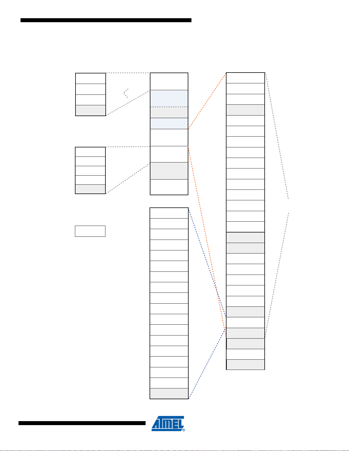
7. Product Mapping
Address memory space
Code
1 MByte
bit band
regiion
1 MByte
bit band
regiion
1 MByte
bit band
regiion
0x00000000
SRAM
0x20000000
0x20100000
0x20400000
0x24000000
0x40000000
offset
ID
peripheral
block
Code
Boot Memory
0x00000000
0x00400000
0x00800000
Reserved
0x00C00000
0x1FFFFFFF
Peripherals
HSMCI
18
0x40000000
SSC
22
0x40004000
SPI
21
0x40008000
0x4000C000
TC0
TC0
0x40010000
23
TC0
TC1
+0x40
24
TC0
TC2
+0x80
25
TC1
TC3
0x40014000
26
TC1
TC4
+0x40
27
TC1
TC5
+0x80
28
TWI0
19
0x40018000
TWI1
20
0x4001C000
PWM
31
0x40020000
USART0
USART1
14
0x40024000
15
0x40028000
0x4002C000
Reserved
Reserved
0x40030000
UDP
33
0x40034000
ADC
29
0x40038000
DACC
30
0x4003C000
ACC
34
0x40040000
CRCCU
35
0x40044000
0x40048000
System Controller
0x400E0000
0x400E2600
0x40100000
0x40200000
0x40400000
0x60000000
External RAM
SMC Chip Select 0
0x60000000
SMC Chip Select 1
Undefined
32 MBytes
bit band alias
0x61000000
SMC Chip Select 2
0x62000000
SMC Chip Select 3
0x63000000
0x64000000
0x9FFFFFFF
System Controller
SMC
10
0x400E0000
MATRIX
0x400E0200
PMC
5
0x400E0400
UART0
UART1
8
0x400E0600
CHIPID
0x400E0740
9
0x400E0800
EFC
6
0x400E0A00
0x400E0C00
PIOA
11
0x400E0E00
PIOB
12
0x400E1000
PIOC
13
0x400E1200
RSTC
0x400E1400
1
SUPC
+0x10
RTT
+0x30
3
WDT
+0x50
4
RTC
+0x60
2
GPBR
+0x90
0x400E1600
0x4007FFFF
Internal Flash
Internal ROM
Reserved
Peripherals
External SRAM
0x60000000
0xA0000000
System
0xE0000000
0xFFFFFFFF
Reserved
Reserved
EFC1
Reserved
Reserved
Reserved
Reserved
32 MBytes
bit band alias
Reserved
Figure 7-1. SAM4S Product Mapping
SAM4S Series [Preliminary]
11100B–ATARM–31-Jul-12
29
Page 30

8. Memories
8.1 Embedded Memories
8.1.1 Internal SRAM
The SAM4SD32 device (2x1024 Kbytes) embeds a total of 160-Kbytes high-speed SRAM.
The SAM4SD16 device (2x512KBytes)embeds a total of 160-Kbytes high-speed SRAM.
The SAM4SA16 device (1024 Kbytes) embeds a total of 160 -Kb yt es hig h -spe ed SRAM.
The SAM4S16 device (1024 Kbytes) embeds a total of 128-Kbytes high-speed SRAM.
The SAM4S8 device (512 Kbytes) embeds a total of 128-Kbytes high-speed SRAM.
The SRAM is accessible over System Cortex-M4 bus at address 0x2000 0000.
The SRAM is in the bit band region. The bit band alias region is from 0x2200 0000 to
0x23FF FFFF.
8.1.2 Internal ROM
The SAM4S embeds an Internal ROM, which contains the SAM Boot Assistant (SAM-BA
Application Programming routines (IAP) and Fast Flash Programming Interface (FFPI).
At any time, the ROM is mapped at address 0x0080 0000.
8.1.3 Embedded Flash
8.1.3.1 Flash Overview
The memory is organized in sectors. Each sector has a size of 64 KBytes. The first sector of 64
KBytes is divided into 3 smaller sectors.
The three smaller sectors are organized to consist of 2 sectors of 8 KBytes and 1 sector of 48
KBytes. Refer to Figure 8-1, "Global Flash Organization" below.
®
), In
30
SAM4S Series [Preliminary]
11100B–ATARM–31-Jul-12
Page 31
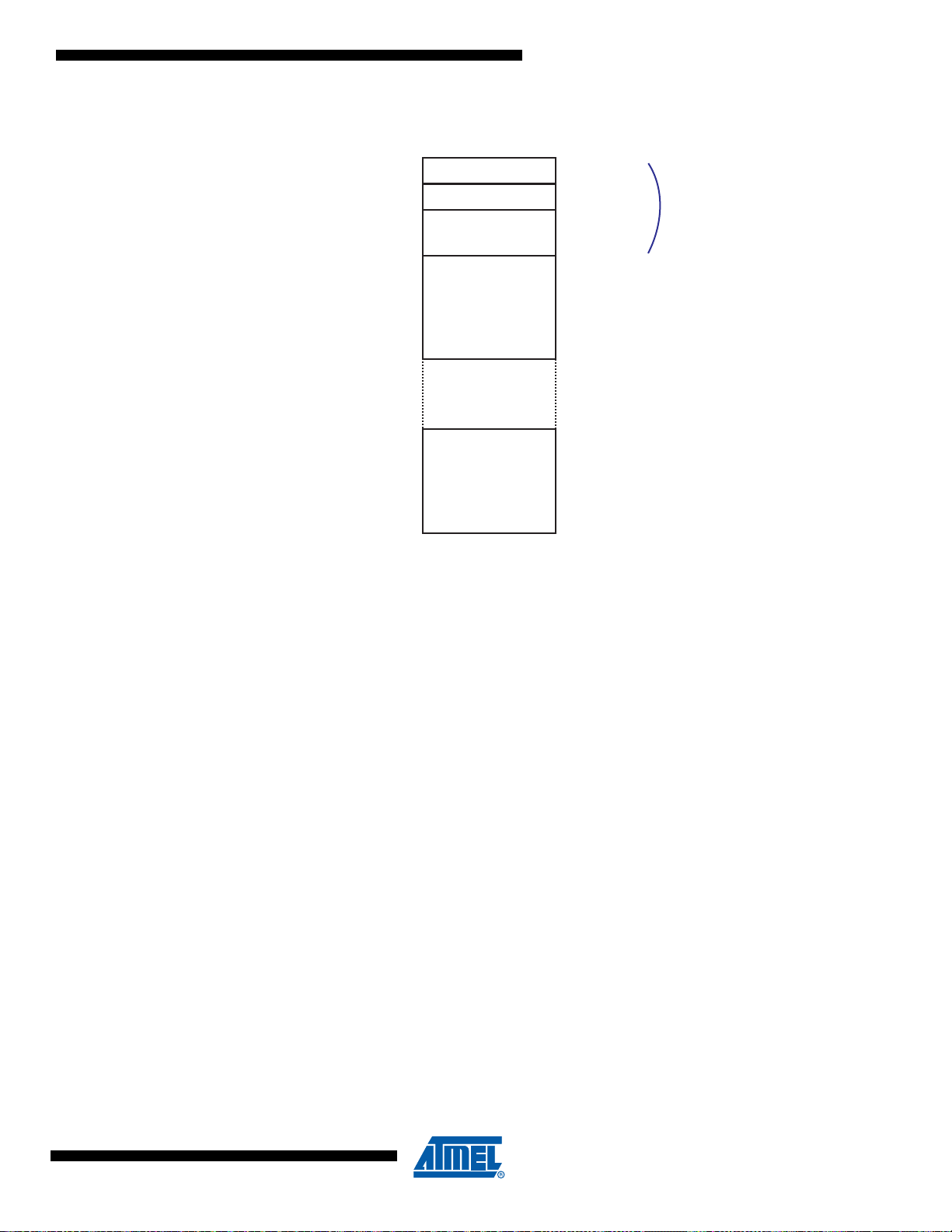
Figure 8-1. Glob al Flash Org a niz atio n
Sector size Sector name
8 KBytes
8 KBytes
SAM4S Series [Preliminary]
Small Sector 0
Small Sector 1
Sector 0
48 KBytes
64 KBytes Sector n
Each Sector is organized in pages of 512 Bytes.
For sector 0:
• The smaller sector 0 has 16 pages of 512Bytes
• The smaller sector 1 has 16 pages of 512 Bytes
• The larger sector has 96 pages of 512 Bytes
From Sector 1 to n:
Larger Sector
Sector 164 KBytes
11100B–ATARM–31-Jul-12
The rest of the array is composed of 64-KByte sectors of 128 pages, each page of 512 bytes.
Refer to Figure 8-2, "Flash Sector Organization" below.
31
Page 32
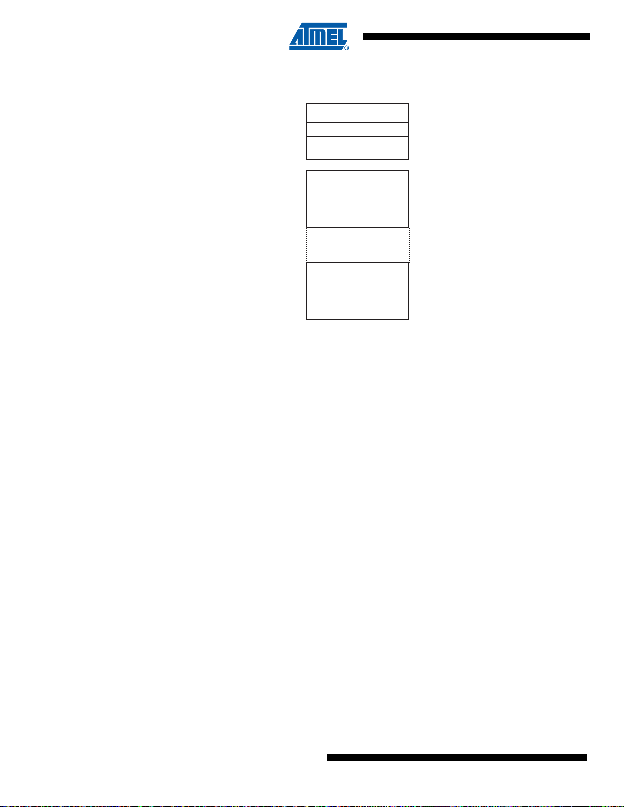
Figure 8-2. Flas h Sec to r Orga nization
Sector 0
Sector 1
Smaller sector 0
Smaller sector 1
Larger sector
A sector size is 64 KBytes
16 pages of 512 Bytes
16 pages of 512 Bytes
96 pages of 512 Bytes
128 pages of 512 Bytes
Sector n 128 pages of 512 Bytes
Flash size varies by product:
• SAM4S8/S16: the Flash size is 512 KBytes
– Internal Flash address is 0x0040_0000
• SAM4SD16/SA16: the Flash size is 2 x 512 KBytes
– Internal Flash0 address is 0x0040_0000
– Internal Flash1 address is 0x0048_0000
• SAM4SD32: the Flash siz e is 2 x 1024 KBytes
– Internal Flash0 address is 0x0040_0000
– Internal Flash1 address is 0x0050_0000
32
SAM4S Series [Preliminary]
11100B–ATARM–31-Jul-12
Page 33
SAM4S Series [Preliminary]
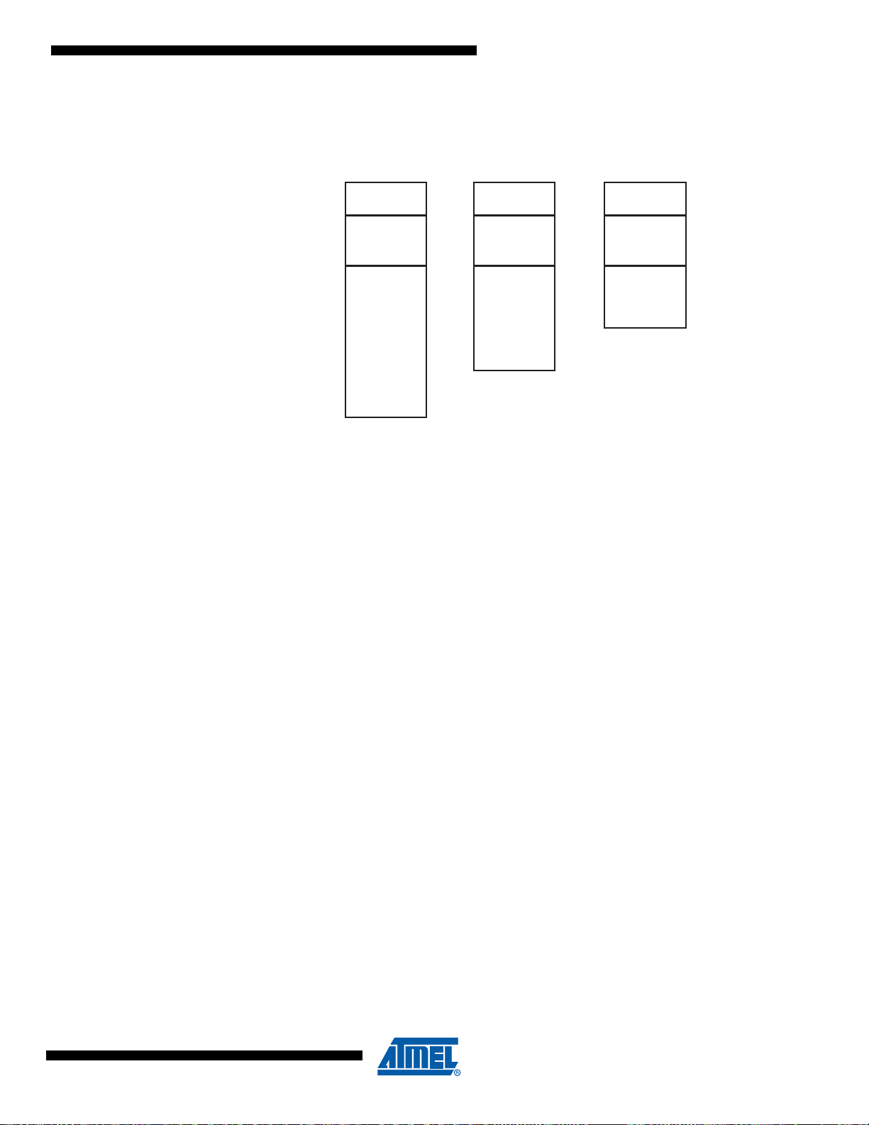
Refer to Figure 8-3, "Flash Size" below for the organization of the Flash following its size.
Figure 8-3. Flas h Size
Flash 1 MBytes Flash 512 KBytes Flash 256 KBytes
2 * 8 KBytes
1 * 48 KBytes
15 * 64 KBytes
Erasing the memory can be performed as follows:
• On a 512-byte page inside a sector, of 8K Bytes
Note: EWP and EWPL commands can be only used in 8 KBytes sectors.
• On a 4-Kbyte Block inside a sector of 8 KBytes/48 Kbytes/64 KBytes
• On a sector of 8 KBytes/48 KBytes/64 KBytes
• On chip
8.1.3.2 Enhanced Embedded Flash Controller
The Enhanced Embedded Flash Controller manages accesses performed by the masters of the
system. It enables reading the Flash and writing the write buffer. It also contains a User Interface, mapped on the APB.
2 * 8 KBytes
1 * 48 KBytes
7 * 64 KBytes
2 * 8 KBytes
1 * 48 KBytes
3 * 64 KBytes
8.1.3.3 Flash Speed
11100B–ATARM–31-Jul-12
The Enhanced Embedded Flash Controller ensures the interface of the Flash block.
It manages the programming, erasing, locking and unlocking seque nces of the Flash using a fu ll
set of commands.
One of the commands returns the embedded Flash descriptor definition that informs the system
about the Flash organization, thus makin g the so ftware generic.
The user needs to set the number of wait states depending on the frequency used:
For more details, refer to the “AC Characteris tics” sub-section of the product “Electrical
Characteristics”.
33
Page 34
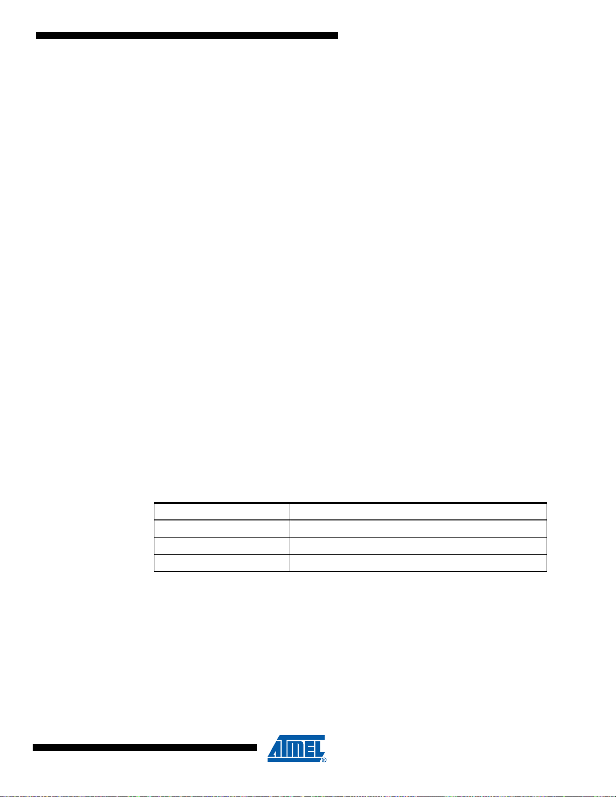
8.1.3.4 Lock Regions
Several lock bits are used to protect write and erase operations on lock regions. A lock region is
composed of several consecutive pages, and each lock region has its associated lock bit.
Table 8-1. Lock Bit Number
If a locked-region’s erase or program command occurs, the command is aborted and the EEFC
triggers an interrupt.
The lock bits are software programmable through the EEFC User Interface. The command “Set
Lock Bit” enables the protection. The command “Clear Lock Bit” unlocks the lock region.
Asserting the ERASE pin clears the lock bits, thus unlocking the entire Flash.
8.1.3.5 Security Bit Feature
The SAM4SD32 and SAM4SD16 feature 2 security bits, the SAM4S16/SA16/S8 feature a security bit, based on a specific General Purpose NVM bit (GPNVM bit 0). When one of the security
bits is enabled, any access to the Flash, SRAM, Core Registers and Internal Peripherals either
through the ICE interface or through the Fast Flash Programming Interface, is forbidden. This
ensures the confidentiality of the code programmed in the Flash.
Product Number of Lock Bits Lock Region Size
SAM4SD32 256 (128 + 128) 8 Kbytes
SAM4SD16 128 (64 + 64) 8 Kbytes
SAM4S16/SA16 128 8 Kbytes
SAM4S8 64 8 Kbytes
This security bit can only be enabled, through the command “Set General Pur pose NVM Bit 0” of
the EEFC User Interface. Disabling the security bit can only be achieved by asserting the
ERASE pin at 1, and after a full Flash erase is performed. When the security bit is deactivated,
all accesses to the Flash, SRAM, Core registers, Internal Peripherals are permitted.
It is important to note that the assertion of the ERASE pin should always be longer than 200 ms.
As the ERASE pin integrates a permanent pull-down, it can be left unconnected during normal
operation. However, it is safer to connect it directly to GND for the final application.
8.1.3.6 Calibration Bits
NVM bits are used to calibrate the brownout detector and the voltage regulator. These bits are
factory configured and cannot be changed by the user. The ERASE pin has no effect on the calibration bits.
8.1.3.7 Unique Identifier
Each device integrates its own 128-bit unique identifier. These bits are factory configured and
cannot be changed by the user. The ERASE pin has no effect on the unique identifier.
8.1.3.8 User Signature
Each part contains a User Signature of 512 bytes. It can be used by the user to store user information such as trimming, keys, etc., th at the customer does not want to be erased by asserting
the ERASE pin or by software ERASE command. Read, write and erase of this area is allowed.
34
SAM4S Series [Preliminary]
11100B–ATARM–31-Jul-12
Page 35
8.1.3.9 Fast Flash Programming Interface
The Fast Flash Programming Interface allows programming the dev ice through a multiplexed
fully-handshaked parallel port. It allows gang programming with market-standard industrial
programmers.
The FFPI supports read, page program, page erase, full erase, lock, unlock and protect
commands.
8.1.3.10 SAM-BA Boot
The SAM-BA Boot is a default Boot Program which provides an easy wa y to pr ogram in-situ th e
on-chip Flash memory.
The SAM-BA Boot Assistant supports serial communication via th e UART and USB.
The SAM-BA Boot provides an interface with SAM-BA Graphic User Interface (GUI).
The SAM-BA Boot is in ROM and is mapped in Flash at address 0x0 when GP NVM bit 1 is set to
0.
8.1.3.11 GPNVM Bits
The SAM4S16 features two GPNVM bits. These bits can be cleared or set respectively through
the commands “Clear GPNVM Bit” and “Set GPNVM Bit” of the EEFC User Interface.
SAM4S Series [Preliminary]
8.1.4 Boot Strate gi es
The Flash of the SAM4S8 is composed of 512 Kbytes in a single bank.
The SAM4SA16/SD32/SD16 features 3 GP NVM bits (G PNV M fro m Flas h0) that can be cle are d
or set respectively through the "Clear GPNVM Bit" and "Set GPNVM Bit" commands of the
EEFC0 User Interface. The GPNVM bits of the SAM4SA16/SD16/SD32 are only ava ilable on
FLash0. There is no GPNVM bit on Flash1. The GPNVM0 is the security bit. The GPNVM1 is
used to select the boot mode (boot always at 0x00) on ROM or FLASH. The SAM4SD32/16
embeds an additional GPNVM bit: GPNVM2. This GPNVM bit is used on ly to swap the Flash0
and Flash1. If GPNVM bit 2 is:
ENABLE: the Flash1 is mapped at address 0x0040_0000 (Flash1 and Flash0 are continuous).
DISABLE: the Flash0 is mapped at address 0x0040_0000 (Flash0 and Flash1 are continuous).
Table 8-2. General-purpose Non volatile Memory Bits
GPNVMBit[#] Function
0 Security bit
1 Boot mode selection
2 Flash selection (Flash 0 or Flash 1)
The system always boots at address 0x0. To ensure maximum boot possibilities, the memory
layout can be changed via GPNVM.
11100B–ATARM–31-Jul-12
A general purpose NVM (GPNVM) bit is used to boot either on the ROM (default) or from the
Flash.
The GPNVM bit can be cleared or set respectively through the commands “Clear General-purpose NVM Bit” and “Set General-purpose NVM Bit” of the EEFC User Inte rface.
Setting GPNVM Bit 1 selects the boot from the Flash, clearing it selects the boot from the ROM.
Asserting ERASE clears the GPNVM Bit 1 and thus selects the boot from the ROM by default.
35
Page 36

Setting the GPNVM Bit 2 selects bank 1, clearing it selects the boot from bank 0. Asserting
ERASE clears the GPNVM Bit 2 and thus selects the boot from bank 0 by default.
8.2 External Memories
The SAM4S features one External Bus Inte rface to pr ovide an in terf ace to a wide ra nge of external memories and to any parallel peripheral.
8.2.1 Static Memory Controller
• 16-Mbyte Address Space per Chip Select
• 8- bit Data Bus
• Word, Halfword, Byte Transfers
• Programmable Setup, Pulse And Hold Time for Read Signals per Chip Select
• Programmable Setup, Pulse And Hold Time for Write Signals per Chip Select
• Programmable Data Float Time per Chip Select
• External Wait Request
• Automatic Switch to Slow Clock Mode
• Asynchronous Read in Page Mode Supported: Page Size Ranges from 4 to 32 Bytes
• NAND Flash additional logic supporting NAND Flash with Multiplexed Data/Address buses
• Hardware Configurable number of chip selects from 1 to 4
• Programmable timing on a per chip select ba sis
9. System Controller
The System Controller is a set of peripherals which allows handling of key elements of the system, such as power, resets, clocks, time, interrupts, watchdog, etc...
See the system controller block diagram in Figure 9-1 on page 37.
36
SAM4S Series [Preliminary]
11100B–ATARM–31-Jul-12
Page 37
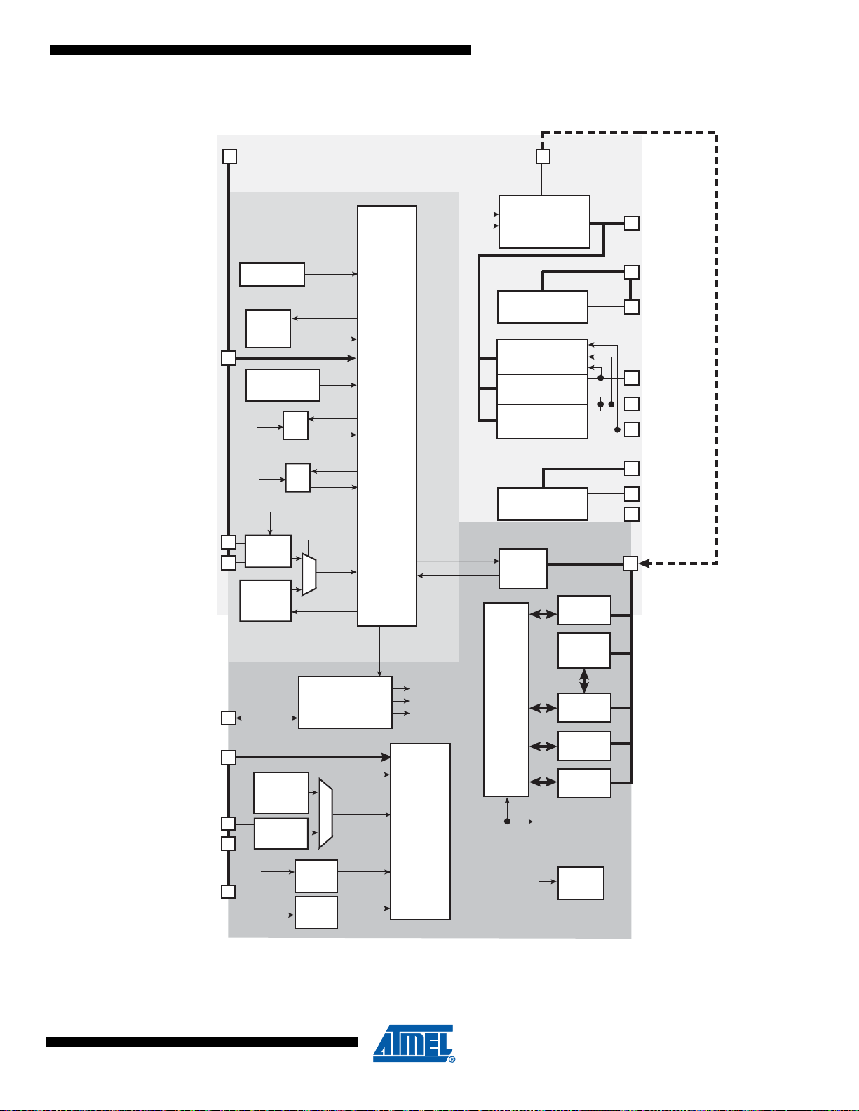
Figure 9-1. System Controller Block Diagram
Software Controlled
Voltage Regulator
Matrix
SRAM
Watchdog
Timer
Cortex-M4
Flash
Peripherals
Peripheral
Bridge
Zero-Power
Power-on Reset
Supply
Monitor
(Backup)
RTC
Power
Management
Controller
Embedded
32 kHz RC
Oscillator
Xtal 32 kHz
Oscillator
Supply
Controller
Brownout
Detector
(Core)
Reset
Controller
Backup Power Supply
Core Power Supply
PLLA
vr_on
vr_mode
ON
out
rtc_alarm
SLCK
rtc_nreset
proc_nreset
periph_nreset
ice_nreset
Master Clock
MCK
SLCK
NRST
MAINCK
FSTT0 - FSTT15
XIN32
XOUT32
osc32k_xtal_en
Slow Clock
SLCK
osc32k_rc_en
VDDIO
VDDCORE
VDDOUT
ADVREF
ADx
WKUP0 - WKUP15
bod_core_on
lcore_brown_out
RTT
rtt_alarm
SLCK
rtt_nreset
XIN
XOUT
VDDIO
VDDIN
PIOx
USB
Transeivers
VDDIO
DDP
DDM
MAINCK
DAC Analog
Circuitry
DACx
PLLB
PLLBCK
PLLACK
Embedded
12 / 8 / 4 MHz
RC
Oscillator
Main Clock
MAINCK
SLCK
3 - 20 MHz
XT AL Oscillator
VDDIO
XTALSEL
General Purpose
Backup Registers
vddcore_nreset
vddcore_nreset
PIOA/B/C
Input/Output Buffers
ADC Analog
Circuitry
Analog
Comparator
FSTT0 - FSTT15 are possible Fast Startup sources, generated by WKUP0 - WKUP15 pins,
but are not physical pins.
SAM4S Series [Preliminary]
11100B–ATARM–31-Jul-12
37
Page 38

9.1 System Controller and Peripheral Mapping
Refer to Figure 7-1, "SAM4S Product Mapping".
All the peripherals are in the bit band region and are mapped in the bit band alias region.
9.2 Power-on-Reset, Brownout and Supply Monitor
The SAM4S embeds three features to monitor, warn and/or reset the chip:
• Power-on-Reset on VDDIO
• Brownout Detector on VDDCORE
• Supply Monitor on VDDIO
9.2.1 Power-on-Reset
The Power-on-Reset monitors VDDIO. It is always activated and monitors voltage at start up but
also during power down. If VDDIO goes below the threshold voltage, the entire chip is reset. For
more information, refer to the Electrical Characteristics section of the datasheet.
9.2.2 Brownout Detector on VDDCORE
The Brownout Detector monitors VDDCORE. It is active by default. It can be deactivated by software through the Supply Controller (SUPC_MR). It is especially recommended to disable it
during low-power modes such as wait or sleep modes.
If VDDCORE goes below the threshold voltage, the reset of the core is asserted. For more information, refer to the Supply Controller (SUPC) and Electrical Characteristics sections of the
datasheet.
9.2.3 Supply Monitor on VDDIO
The Supply Monitor monitors VDDIO. It is not active by default. It can be activated by software
and is fully programmable with 16 steps for the threshold (between 1.6V to 3.4V). It is controlled
by the Supply Controller (SUPC). A sample mode is possible. It allows to divide the supply monitor power consumption by a factor of up to 2048. For more information, refer to the SUPC and
Electrical Characteristics sections of the datasheet.
38
SAM4S Series [Preliminary]
11100B–ATARM–31-Jul-12
Page 39

SAM4S Series [Preliminary]
10. Peripherals
10.1 Peripheral Identifiers
Table 10-1 defines the Peripheral Identifiers of th e SAM 4S. A p e rip he ra l id en tif ier is re qu ire d fo r
the control of the peripheral interrupt with th e Nested Ve ctored Interr upt Con troller a nd cont rol of
the peripheral clock with the Power Management Controller.
Table 10-1. Peripheral Identifiers
PMC
Instance ID Instance Name NVIC Interrupt
0SUPC X Supply Controller
1RSTC X Reset Controller
2RTC X Real Time Clock
3RTT X Real Time Timer
4WDT X Watchdog Timer
5PMC X Power Management Controller
6EEFC0 X Enha nced Embedded Flash Controller 0
7EEFC1 - Enha nced Embedded Flash Controller 1
8UART0 X XUART 0
9UART1 X XUART 1
10 SMC X X Static Memory Controller
11 PIOA X X Parallel I/O Controller A
12 PIOB X X Parallel I/O Controller B
13 PIOC X X Parallel I/O Controller C
14 USART0 X X USART 0
15 USART1 X X USART 1
16 - - - Reserved
17 - - - Reserved
18 HSMCI X X Multimedia Card Interface
19 TWI0 X X Two Wire Interface 0
20 TWI1 X X Two Wire Interface 1
21 SPI X X Serial Peripheral Interface
22 SSC X X Synchronous Serial Controller
23 TC0 X X Timer/Counter 0
24 TC1 X X Timer/Counter 1
25 TC2 X X Timer/Counter 2
26 TC3 X X Timer/Counter 3
27 TC4 X X Timer/Counter 4
28 TC5 X X Timer/Counter 5
29 ADC X X Analog To Digital Converter
30 DACC X X Digi ta l To Analog Converter
Clock Control Instance Description
11100B–ATARM–31-Jul-12
39
Page 40

Table 10-1. Peripheral Identifiers (Continued)
PMC
Instance ID Instance Name NVIC Interrupt
31 PWM X X Pulse Width Modulation
32 CRCCU X X CRC Calculation Unit
33 ACC X X Analog Comparator
34 UDP X X USB Device Port
Clock Control Instance Description
10.2 Peripheral Signal Multiplexing on I/O Lines
The SAM4S features 2 PIO controllers on 64-pin versions (PIOA and PIOB) or 3 PIO controllers
on the 100-pin version (PIOA, PIOB and PIOC), t hat multiple x th e I/O lines of the peripher al set.
The SAM4S 64-pin and 100-pin PIO Controllers control up to 32 lines. Each line can be
assigned to one of three peripheral functions: A, B or C. The multiplexing tables in the following
paragraphs define how the I/O lines of the peripherals A, B and C are multiplexed on the PIO
Controllers. The column “Comments” has been inserted in this table for the user’s own comments; it may be used to track how pins are defined in an application.
Note that some peripheral functions which are output only, might be duplicated within the tables.
40
SAM4S Series [Preliminary]
11100B–ATARM–31-Jul-12
Page 41

SAM4S Series [Preliminary]
10.2.1 PIO Controller A Multiplexing Table 10-2. Multiplexing on PIO Controller A (PIOA)
I/O Line Peripheral A Peripheral B Peripheral C Extra Function System Function Comments
PA0 PWMH0 TIOA0 A17 WKUP0
PA1 PWMH1 TIOB0 A18 WKUP1
PA2 PWMH2 SCK0 DATRG WKUP2
PA3 TWD0 NPCS3
PA4 TWCK0 TCLK0 WKUP3
PA5 RXD0 NPCS3 WKUP4
PA6 TXD0 PCK0
PA7 RTS0 PWMH3 XIN32
PA8 CTS0 ADTRG WKUP5 XOUT32
PA9 URXD0 NPCS1 PWMFI0 WKUP6
PA10 UTXD0 NPCS2
PA11 NPCS0 PWMH0 WKUP7
PA12 MISO PWMH1
PA13 MOSI PWMH2
PA14 SPCK PWMH3 WKUP8
PA15 TF TIOA1 PWML3 WKUP14/PIODCEN1
PA16 TK TIOB1 PWML2 WKUP15/PIODCEN2
PA17 TD PCK1 PWMH3 AD0
PA18 RD PCK2 A14 AD1
PA19 RK PWML0 A15 AD2/WKUP9
PA20 RF PWML1 A16 AD3/WKUP10
PA21 RXD1 PCK1 AD8 64/100 pins versions
PA22 TXD1 NPCS3 NCS2 AD9 64/100 pins versions
PA23 SCK1 PWMH0 A19 PIODCCLK 64/100 pins versions
PA24 RTS1 PWMH1 A20 PIODC0 64/100 pins versions
PA25 CTS1 PWMH2 A23 PIODC1 64/100 pins versions
PA26 DCD1 TIOA2 MCDA2 PIODC2 64/100 pins versions
PA27 DTR1 TIOB2 MCDA3 PIODC3 64/100 pins versions
PA28 DSR1 TCLK1 MCCDA PIODC4 64/100 pins versions
PA29 RI1 TCLK2 MCCK PIODC5 64/100 pins versions
PA30 PWML2 NPCS2 MCDA0 WKUP11/PIODC6 64/100 pins versions
PA31 NPCS1 PCK2 MCDA1 PIODC7 64/100 pins versions
11100B–ATARM–31-Jul-12
41
Page 42

10.2.2 PIO Controller B Multiplexing Table 10-3. Multiplexing on PIO Controller B (PIOB)
I/O
Line Periph er a l A Peripheral B Peripheral C Extra Function System Function Comments
PB0 PWMH0 AD4/RTCOUT0
PB1 PWMH1 AD5/RTCOUT1
PB2 URXD1 NPCS2 AD6/WKUP12
PB3 UTXD1 PCK2 AD7
PB4 TWD1 PWMH2 TDI
PB5 TWCK1 PWML0 WKUP13 TDO/TRACESWO
PB6 TMS/SWDIO
PB7 TCK/SWCLK
PB8 XOUT
PB9 XIN
PB10 DDM
PB11 DDP
PB12 PWML1 ERASE
PB13 PWML2 PCK0 DAC0 64/100 pins versions
PB14 NPCS1 PWMH3 DAC1 64/100 pins versions
42
SAM4S Series [Preliminary]
11100B–ATARM–31-Jul-12
Page 43

10.2.3 PIO Controller C Multiplexing Table 10-4. Multiplexing on PIO Controller C (PIOC)
SAM4S Series [Preliminary]
Extra
I/O Line Peripheral A Peripheral B Peripheral C
PC0 D0 PWML0 100 pin version
PC1 D1 PWML1 100 pin version
PC2 D2 PWML2 100 pin version
PC3 D3 PWML3 100 pin version
PC4 D4 NPCS1 100 pin version
PC5 D5 100 pin version
PC6 D6 100 pin version
PC7 D7 100 pin version
PC8 NWE 100 pin version
PC9 NANDOE 100 pin version
PC10 NANDWE 100 pin version
PC11 NRD 100 pin version
PC12 NCS3 AD12 100 pin version
PC13 NWAIT PWML0 AD10 100 pin version
PC14 NCS0 100 pin version
PC15 NCS1 PWML1 AD11 100 pin version
Function
System
Function Comments
PC16 A21/NANDALE 100 pin version
PC17 A22/NANDCLE 100 pin version
PC18 A0 PWMH0 100 pin version
PC19 A1 PWMH1 100 pin version
PC20 A2 PWMH2 100 pin version
PC21 A3 PWMH3 100 pin version
PC22 A4 PWML3 100 pin version
PC23 A5 TIOA3 100 pin version
PC24 A6 TIOB3 100 pin version
PC25 A7 TCLK3 100 pin version
PC26 A8 TIOA4 100 pin version
PC27 A9 TIOB4 100 pin version
PC28 A10 TCLK4 100 pin version
PC29 A11 TIOA5 AD13 100 pin version
PC30 A12 TIOB5 AD14 100 pin version
PC31 A13 TCLK5 100 pin version
11100B–ATARM–31-Jul-12
43
Page 44

44
SAM4S Series [Preliminary]
11100B–ATARM–31-Jul-12
Page 45

11. ARM Cortex-M4
11.1 Description
The Cortex-M4 processor is a high performance 32-bit processor designed for the microcontroller market. It offers significant benefits to developers, including outstanding processing
performance combined with fast interrupt handling, enhance d system debug with extensive
breakpoint and trace capabilities, efficient processor core, system and memories, ultra-low
power consumption with integrated sleep modes, and platform security robustness, with inte-
grated memory protection unit (MPU).
The Cortex-M4 processor is built on a high-performance processor core, with a 3-stage pipeline
Harvard architecture, making it ideal for demanding embedded applications. The p rocessor
delivers exceptional power efficiency through an efficient instruction set and extensively optimized design, providing high-end processing hardware including a range of single-cycle and
SIMD multiplication and multiply-with-accumulate capabilities, saturating arithmetic and dedicated hardware division.
To facilitate the design of cost-sensitive devices, the Cortex-M4 processor implements tightlycoupled system components that reduce processor area while significantly improving interrupt
handling and system debug capabilities. The Cortex-M4 processor implements a version of the
Thumb
program memory requirements. The Cortex-M4 instruction set provides the exceptional performance expected of a modern 32-bit architecture, with the high code density of 8-bit and 16-bit
microcontrollers.
SAM4S Series [Preliminary]
®
instruction set based on Thumb-2 technology, ensuring high code density and reduced
The Cortex-M4 processor closely integrates a configurable NVIC , to deliver industry-leading
interrupt performance. The NVIC includes a non-maskable interrupt (NMI), and provides up to
256 interrupt priority levels. The tight integration of the processor core and NVIC provides fast
execution of interrupt service routines (ISRs), dramatically reducing the interrupt latency. This is
achieved through the hardware stacking of registers, and the ability to suspend load-multiple
and store-multiple operations. Interrupt handlers do not require wrapping in assembler code,
removing any code overhead from the ISRs. A tail-chain optimization also significantly reduces
the overhead when switching from one ISR to an other.
To optimize low-power designs, the NVIC integrates with the sleep modes, that include a deep
sleep function that enables the entire device to be rapidly powered down while still retaining program state.
11.1.1 System Level Interface
The Cortex-M4 processor provides multiple interfaces using AMBA
speed, low latency memory accesses. It supports unaligned data accesses and implements
atomic bit manipulation that enables faster peripheral controls, system spinlocks and thread-safe
Boolean data handling.
The Cortex-M4 processor has a Memory Protection Unit (MPU) that provides fine grain memory
control, enabling applications to utilize multiple privilege levels, separating and protecting code,
data and stack on a task-by-task basis. Such requirements are becoming critical in many
embedded applications such as automotive.
®
technology to provide high
11100B–ATARM–31-Jul-12
45
Page 46

11.1.2 Integrated Configurable Debug
The Cortex-M4 processor implements a complete hardware debug solution. This provides high
system visibility of the processor and memory through either a traditional JTAG port or a 2-pin
Serial Wire Debug (SWD) port that is ideal for mi crocontrollers and other small package devices.
For system trace the processor integrates an Instrumentation Trace Macrocell (ITM) alongside
data watchpoints and a profiling unit. To enable simple and cost-effective profiling of the system
events these generate, a Serial Wire Viewer (SWV) can export a stream of software-generated
messages, data trace, and profiling information through a single pin.
The Flash Patch and Breakpoint Unit (FPB) provides up to 8 hardware breakpoint comparators
that debuggers can use. The comparators in the FPB also provide remap functions of up to 8
words in the program code in the CODE memory region. This enables applications stored on a
non-erasable, ROM-based microcontroller to be patched if a small programmable memory, for
example flash, is available in the device. During initialization, the application in ROM detects,
from the programmable memory, whether a patch is required. If a patch is required, the application programs the FPB to remap a nu mber of addr esses. When those ad dresses ar e accessed ,
the accesses are redirected to a remap table specified in the FPB configuration, which means
the program in the non-modifiable ROM can be patched.
11.2 Embedded Characteristics
• Tight integration of system peripherals reduces area and development costs
• Thumb instruction set combines high code density with 32-bit performance
• Code-patch ability for ROM system updates
• Power control optimization of system components
• Integrated sleep modes for low power consumption
• Fast code execution permits slower processor clock or increases sleep mode time
• Hardware division and fast digital-signal-processing oriented multiply accumulate
• Saturating arithmetic for signal processing
• Deterministic, high-performance interrupt handling for time-critical applications
• Memory Protection Unit (MPU) for safety-critical applications
• Extensive debug and trace capabilities:
– Serial Wire Debug and Serial Wire Trace reduce the number of pins required for
debugging, tracing, and code profiling.
46
SAM4S Series [Preliminary]
11100B–ATARM–31-Jul-12
Page 47
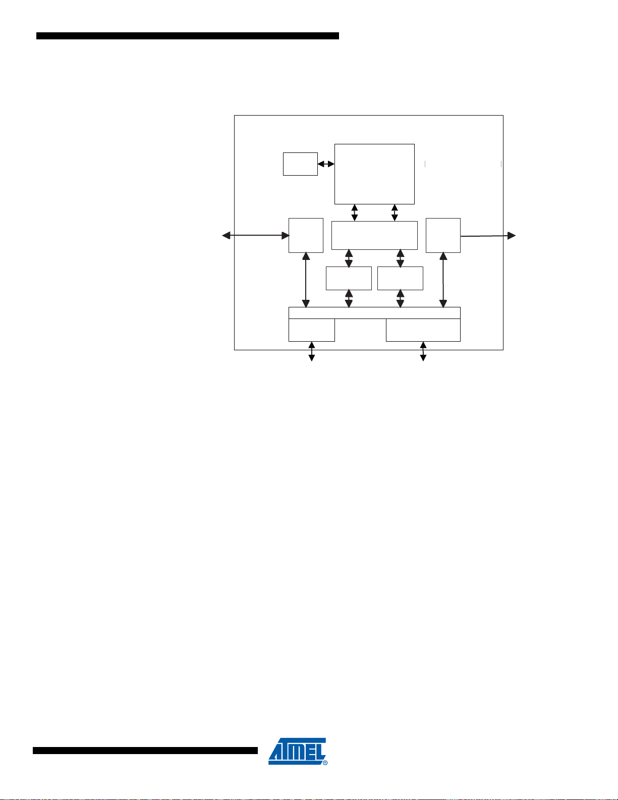
11.3 Block Diagram
NVIC
Debug
Access
Port
Memory
Protection Unit
Serial
Wire
Viewer
Bus Matrix
Code
Interface
SRAM and
Peripheral Interface
Data
Watchpoints
Flash
Patch
Cortex-M4
Processor
Processor
Core
SAM4S Series [Preliminary]
Figure 11-1. Typical Cortex-M4 Implementation
11100B–ATARM–31-Jul-12
47
Page 48

11.4 Cortex-M4 Models
11.4.1 Programmers Model
This section describes the Cortex-M4 programmers model. In addition to the individual core register descriptions, it contains information about the processo r modes and privilege levels for
software execution and stacks.
11.4.1.1 Processor Modes And Privilege Levels for Software Execution
The processor modes are:
• Thread mode
Used to execute application software. The processo r enter s the Threa d mode when it come s
out of reset.
• Handler mode
Used to handle exceptions. The processor returns to the Thread mode when it has finished
exception processing.
The privilege levels for software execution are:
• Unprivileged
The software:
– has limited access to the MSR and MRS instructions, and cannot use the CPS
instruction
– cannot access the System Timer, NVIC, or System Control Block
– might have a restricted access to memory or peripherals.
Unprivileged software executes at the unprivileged level.
11.4.1.2 Stacks
• Privileged
The software can use all the instructions and has access to all resources. Privileged software
executes at the privileged level.
In Thread mode, the CONTROL register controls whether the soft war e execution is privileged or
unprivileged, see “CONTROL Register” . In Handler mode, software execution is always
privileged.
Only privileged software can write to the CONTROL register to change the privilege level for
software execution in Thread mode. Unprivileged software can use the SVC instruction to make
a supervisor call to transfer control to privileged software.
The processor uses a full descending stack. This means the stack pointer holds the address of
the last stacked item in memory When the processor push es a new item ont o the sta ck, it decr ements the stack pointer and then writes the item to the new memory location. The processor
implements two stacks, the main stack and the process stack, with a pointer for each held in
independent registers, see “Stack Pointer” .
In Thread mode, the CONTROL register controls whether the processor uses the main stack or
the process stack, see “CONTROL Register” .
In Handler mode, the processor always uses the main stack.
48
SAM4S Series [Preliminary]
11100B–ATARM–31-Jul-12
Page 49
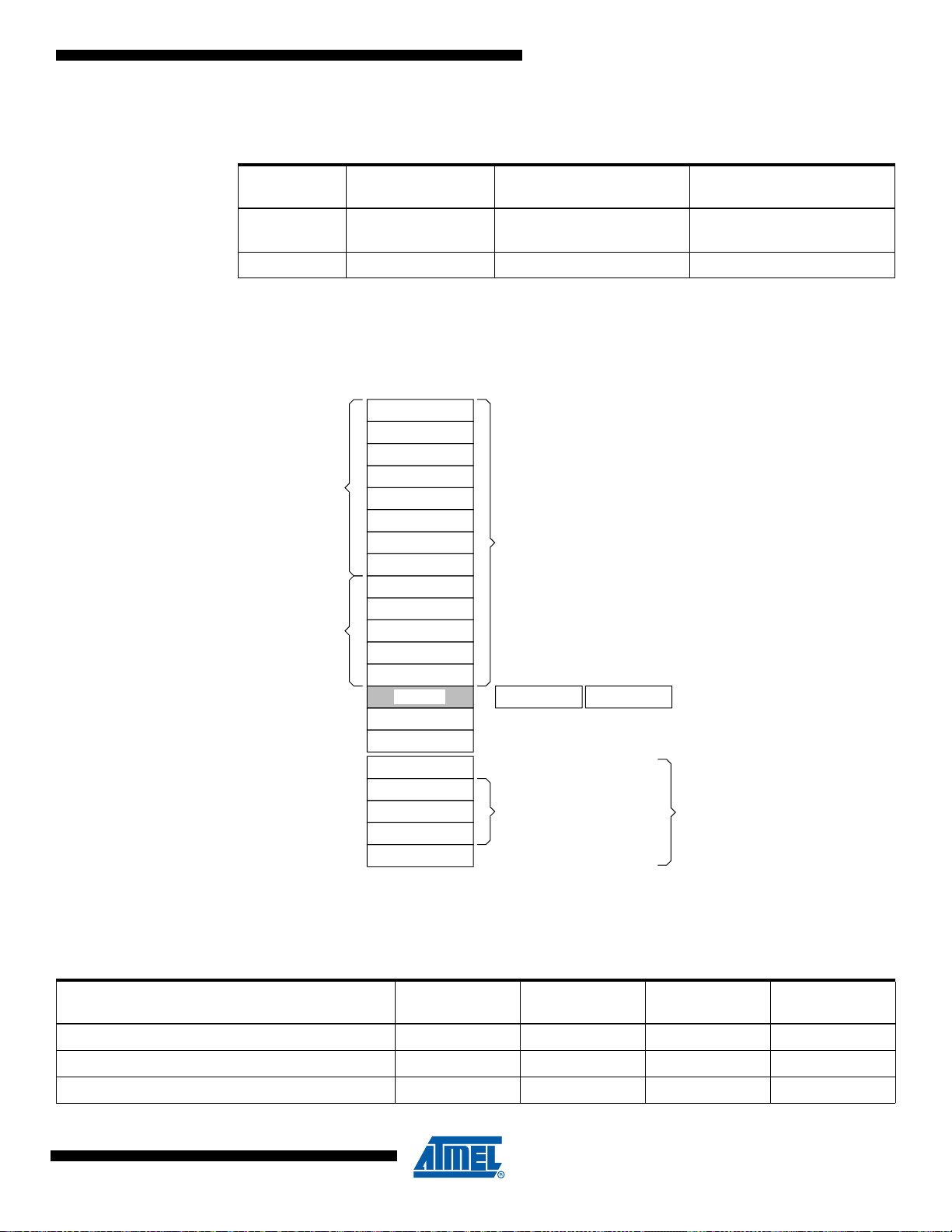
SAM4S Series [Preliminary]
SP (R13)
LR (R14)
PC (R15)
R5
R6
R7
R0
R1
R3
R4
R2
R10
R11
R12
R8
R9
Low registers
High registers
MSP
‡
PSP
‡
PSR
PRIMASK
FAULTMASK
BASEPRI
CONTROL
General-purpose registers
Stack Pointer
Link Register
Program Counter
Program status register
Exception mask registers
CONTROL register
Special registers
‡
Banked version of SP
The options for processor operations are:
Table 11-1. Summary of processor mode, execution privilege level, and stack use options
Note: 1. See “CONTROL Register” .
11.4.1.3 Core Registers
Figure 11-2. Processor Core Registers
Processor
Mode
Thread Applications Privileged or unprivileged
Used to
Execute
Privilege Level for
Software Execution Stack Used
Main stack or
(1)
process stack
Handler Exception handlers Always privileged Main stack
(1)
Table 11-2. Core Processor Registers
Register Name Access
General-purpose registers R0-R12 Read-write Either Unknown
Stack Pointer MSP Read-write Privileged See description
Stack Pointer PSP Read-write Either Unknown
11100B–ATARM–31-Jul-12
(1)
Required
Privilege
(2)
Reset
49
Page 50
Table 11-2. Core Processor Registers
Register Name Access
Link Register LR Read-write Either 0xFFFFFFFF
Program Counter PC Read-write Either See description
Program Status Register PSR Read-write Privileged
Application Program Status Register APSR Read-write Either 0x00000000
Interrupt Program Status Register IPSR Read-only Privileged 0x00000000
Execution Program Status Register EPSR Read-only Privileged 0x01000000
Priority Mask Register PRIMASK Read-write Privileged 0x00000000
Fault Mask Register FAULTMASK Read-write Privileged 0x00000000
Base Priority Mask Register BASEPRI Read-write Privileged 0x00000000
CONTROL register CONTROL Read-write Privileged 0x00000000
Notes: 1. Describes access type during program execution in thread mode and Handler mode. Debug access can differ.
2. An entry of Either means privileged and unprivileged software can access the register.
(1)
Required
Privilege
(2)
Reset
0x01000000
11.4.1.4 General-purpose Registers
R0-R12 are 32-bit general-purpose registers for data operations.
11.4.1.5 Stack Pointer
The Stack Pointer (SP) is register R13. In Thread mode, bit[1] of the CONTROL register indi-
cates the stack pointer to use:
•0 = Main Stack Pointer (MSP). This is the reset value.
•1 = Process Stack Pointer (PSP).
On reset, the processor loads the MSP with the value from address
11.4.1.6 Link Register
The Link Register (LR) is register R14. It stores the return information for subroutines, function
calls, and exceptions. On reset, the processor loads the LR value
11.4.1.7 Program Counter
The Program Counter (PC) is register R15. It contains the current program address. On reset,
the processor loads the PC with the value of the reset vector, which is at address 0x00000004.
Bit[0] of the value is loaded into the EPSR T-bit at reset and must be 1.
0x00000000
0xFFFFFFFF
.
.
50
SAM4S Series [Preliminary]
11100B–ATARM–31-Jul-12
Page 51
11.4.1.8 Program Status Register
Name: PSR
Access: Read-write
SAM4S Series [Preliminary]
Reset:
31 30 29 28 27 26 25 24
N Z C V Q ICI/IT T
23 22 21 20 19 18 17 16
15 14 13 12 11 10 9 8
76543210
0x000000000
–
ICI/IT – ISR_NUMBER
ISR_NUMBER
The Program Status Register (PSR) combines:
• Application Program Status Register (APSR)
• Interrupt Program Status Register (IPSR)
• Execution Program Status Register (EPSR).
These registers are mutually exclusive bitfields in the 32-bit PSR.
Access these registers individually or as a combination of any two or all three regist ers, using the register name as an argu-
ment to the MSR or MRS instructions. For example:
• read all of the registers using PSR with the MRS instruction
• write to the APSR N, Z, C, V and Q bits using APSR_nzcvq with the MSR instruction.
The PSR combinations and attributes are:
Name Access Combination
PSR Read-write
IEPSR Read-only EPSR and IPSR
IAPSR Read-write
EAPSR Read-write
Notes: 1. he processor ignores writes to the IPSR bits.
2. Reads of the EPSR bits return zero, and the processor ignores writes to the these bits
(1)(2)
(1)
(2)
APSR, EPSR, and IPSR
APSR and IPSR
APSR and EPSR
See the instruction descriptions “MRS” and “MSR” for more information about how to access t he pro gram st atus re gisters.
11100B–ATARM–31-Jul-12
51
Page 52
11.4.1.9 Application Program Status Register
Name: APSR
Access: Read-write
Reset:
31 30 29 28 27 26 25 24
NZCVQ –
23 22 21 20 19 18 17 16
15 14 13 12 11 10 9 8
76543210
0x000000000
– GE[3:0]
–
–
The APSR contains the current state of the condition flags fro m previous instruction executions.
• N: Negative Flag
0: operation result was positive, zero, greater than, or equal
1: operation result was negative or less than.
• Z: Zero Flag
0: operation result was not zero
1: operation result was zero.
• C: Carry or Borrow Flag
Carry or borrow flag:
0: add operation did not result in a carry bit or subtract operation resulted in a borrow bit
1: add operation resulted in a carry bit or subtract operation did not result in a borrow bit.
• V: Overflow Flag
0: operation did not result in an overflow
1: operation resulted in an overflow.
• Q: DSP Overflow and Saturation Flag
Sticky saturation flag:
0: indicates that saturation has not occurred since reset or since the bi t was last cleared to zero
SSAT
or
USAT
1: indicates when an
This bit is cleared to zero by software using an
instruction results in saturation.
MRS
instruction.
• GE[19:16]: Greater Than or Equal Flags
See “SEL” for more information.
52
SAM4S Series [Preliminary]
11100B–ATARM–31-Jul-12
Page 53
11.4.1.10 Interrupt Program Status Register
Name: IPSR
Access: Read-write
SAM4S Series [Preliminary]
Reset:
31 30 29 28 27 26 25 24
23 22 21 20 19 18 17 16
15 14 13 12 11 10 9 8
76543210
0x000000000
–
–
– ISR_NUMBER
ISR_NUMBER
The IPSR contains the exception type number of the current Interrupt Service Routine (ISR).
• ISR_NUMBER: Number of the Current Exception
0 = Thread mode
1 = Reserved
2 = NMI
3 = Hard fault
4 = Memory management fault
5 = Bus fault
6 = Usage fault
7-10 = Reserved
11 = SVCall
12 = Reserved for Debug
13 = Reserved
14 = PendSV
15 = SysTick
16 = IRQ0
50 = IRQ34
See “Exception Types” for more information.
11100B–ATARM–31-Jul-12
53
Page 54
11.4.1.11 Execution Program Status Register
Name: EPSR
Access: Read-write
Reset:
31 30 29 28 27 26 25 24
23 22 21 20 19 18 17 16
15 14 13 12 11 10 9 8
76543210
0x000000000
– ICI/IT T
–
ICI/IT –
–
The EPSR contains the Thumb state bit, and the execution state bits for either the If-Then (IT) instruction, or the Interrupt-
ible-Continuable Instruction (ICI) field for an interrupted load multiple or store multiple instruction.
Attempts to read the EPSR directly through application software using the MSR instruction always return zero. Attempts to
write the EPSR using the MSR instruction in the application software are ignored. Fault handlers can examine the EPSR
value in the stacked PSR to indicate the operation that is at fault. See “Exception Entry and Return”
• ICI: Interruptible-continuable Instruction
When an interrupt occurs during the execution of an LDM, STM, PUSH, POP, VLDM, VSTM, VPUSH,
or VPOP instruction, the processor:
– stops the load multiple or store multiple instruction operation temporarily
– stores the next register operand in the multiple operation to EPSR bits[15:12].
After servicing the interrupt, the processor:
– returns to the register pointed to by bits[15:12]
– resumes the execution of the multiple load or store instruction.
When the EPSR holds the ICI execution state, bits[26:25,11:10] are zero.
• IT: If-Then Instruction
Indicates the execution state bits of the
IT
instruction.
The If-Then block contains up to four instructio ns following an IT instruction. Each instruction in the block is conditional. The
conditions for the instructions are either all the same, or some can be the inverse of others. See “” for more information.
• T: Thumb State
The Cortex-M4 processor only supports the execution of instructions in Thumb state. The following can clear the T bit to 0:
– instructions BLX, BX and POP{PC}
– restoration from the stacked xPSR value on an exception return
– bit[0] of the vector value on an exception entry or reset.
Attempting to execute instructions when the T bit is 0 results in a fault or lockup. See “Lockup” for more information.
54
SAM4S Series [Preliminary]
11100B–ATARM–31-Jul-12
Page 55
11.4.1.12 Exception Mask Registers
The exception mask registers disable the handling of exce ptions by the processor. Disable
exceptions where they might impact on timing critical tasks.
To access the exception mask registers use the MSR and MRS instructions, or the CPS instruction to change the value of PRIMASK or FAULTMASK. See “MRS” , “MSR” , and “CPS” for
more information.
11.4.1.13 Priority Mask Register
Name: PRIMASK
Access: Read-write
SAM4S Series [Preliminary]
Reset:
31 30 29 28 27 26 25 24
23 22 21 20 19 18 17 16
15 14 13 12 11 10 9 8
76543210
0x000000000
–
–
–
– PRIMASK
The PRIMASK register prevents the activation of all exceptions with a configurable priority.
•PRIMASK
0: no effect
1: prevents the activation of all exceptions with a configura ble priority.
11100B–ATARM–31-Jul-12
55
Page 56
11.4.1.14 Fault Mask Register
Name: FAULTMASK
Access: Read-write
Reset:
31 30 29 28 27 26 25 24
23 22 21 20 19 18 17 16
15 14 13 12 11 10 9 8
76543210
0x000000000
–
–
–
– FAULTMASK
The FAULTMASK register prevents the activation of all exceptions except for Non-Maskable Interrupt (NMI).
•FAULTMASK
0: No effect.
1: Prevents the activation of all exceptions except for NMI.
The processor clears the FAULTMASK bit to 0 on exit from any exception handler except the NMI handler.
56
SAM4S Series [Preliminary]
11100B–ATARM–31-Jul-12
Page 57
11.4.1.15 Base Priority Mask Register
Name: BASEPRI
Access: Read-write
SAM4S Series [Preliminary]
Reset:
31 30 29 28 27 26 25 24
23 22 21 20 19 18 17 16
15 14 13 12 11 10 9 8
76543210
0x000000000
–
–
–
BASEPRI
The BASEPRI register defines the minimum priority for exception processing. When BASEPRI is set to a nonzero value, it
prevents the activation of all exceptions with same or lower priority level as the BASEPRI value.
• BASEPRI
Priority mask bits:
0x0000
= no effect.
Nonzero = defines the base priority for exception processing.
The processor does not process any exception with a priority value greater than or equal to BASEPRI.
This field is similar to the pr iority f ields in the inte rrupt prio rity regist ers. The processor implements only b its[7:4] of this field,
bits[3:0] read as zero and ignore writes. See “Interrupt Priority Registers” for more information. Remember that higher pri-
ority field values correspond to lower exception prioriti es.
11100B–ATARM–31-Jul-12
57
Page 58
11.4.1.16 CONTROL Register
Name: CONTROL
Access: Read-write
Reset:
31 30 29 28 27 26 25 24
23 22 21 20 19 18 17 16
15 14 13 12 11 10 9 8
76543210
0x000000000
–
–
–
– – SPSEL nPRIV
The CONTROL register controls the stack used and the privilege level for software execution when the processor is in
Thread mode.
• SPSEL: Active Stack Pointer
Defines the current stack:
0: MSP is the current stack pointer.
1: PSP is the current stack pointer.
In Handler mode, this bit reads as zero and ignores writes. The Cortex-M4 updates this bit automatically on exception
return.
• nPRIV: Thread Mode Privilege Level
Defines the Thread mode privilege level:
0: privileged.
1: unprivileged.
Handler mode always uses the MSP, so the processor ignores explicit writes to the active stack pointer bit of the CON-
TROL register when in Handler mode. The exception entry and return mechanisms update the CONTROL register based
on the EXC_RETURN value.
In an OS environment, ARM rec ommen ds t hat t hread s run ning in T hread mod e u se th e pr oces s stac k, and th e ker nel a nd
exception handlers use the main stack.
By default, the Thread mode uses the MSP. To switch the stack pointer used in Thread mode to the PSP, either:
• use the MSR instruction to set the Active stack pointer bit to 1, see “MSR” , or
• perform an exception return to Thread mode with the appropriate EXC_RETURN valu e, see Table 11-10.
Note: When changing the stack pointer, the software must use an ISB instruction immediately after the MSR instruction. This ensures
that instructions after the ISB execute using the new stack pointer. See “ISB” .
58
SAM4S Series [Preliminary]
11100B–ATARM–31-Jul-12
Page 59

11.4.1.17 Exceptions and Interrupts
The Cortex-M4 processor supports interrupts and system exceptions. The processor and the
Nested Vectored Interrupt Controller (NVIC) prioritize and handle all exceptions. An exception
changes the normal flow of software control. The processor u ses the Ha ndler mode to han dle all
exceptions except for reset. See “Exception Entry” and “Exception Return” for more
information.
The NVIC registers control interrupt handling. See “Nested Vect ored Inter rupt Controller (NVIC)”
for more information.
11.4.1.18 Data Types
The processor supports the following data types:
• 32-bit words
• 16-bit halfwords
• 8-bit bytes
• The processor manages all data memory accesses as little-endian. Instruction memory and
Private Peripheral Bus (PPB) accesses are always little-endian. See “Memory Regions,
Types and Attributes” for more information.
SAM4S Series [Preliminary]
11.4.1.19 Cortex Microcontroller Software Interface Standard (CMSIS) For a Cortex-M4 microcontroller system, the Cortex Microcontroller Software Interface Standard (CMSIS) defines:
• a common way to:
– access peripheral registers
– define exception vectors
• the names of:
– the registers of the core peripherals
– the core exception vectors
• a de vice-independent interface for RTOS kernels, including a debug channel.
The CMSIS includes address definitions and data structures for the core peripherals in the Cortex-M4 processor.
The CMSIS simplifies the software development by enabling the reuse of temp lat e code and the
combination of CMSIS-compliant software components from various middleware vendors. Software vendors can expand the CMSIS to include th eir per iphe ra l def init ions and access f unc tions
for those peripherals.
This document includes the register names defined by the CMSIS, and gives short descriptions
of the CMSIS functions that address the processor core and the core peripherals.
Note: This document uses the register short names defined by the CMSIS. In a few cases, these differ
from the architectural short names that might be used in other documents.
The following sections give more information about the CMSIS:
11100B–ATARM–31-Jul-12
• Section 11.5.3 ”Power Management Programming Hints”
• Section 11.6.2 ”CMSIS Functions”
• Section 11.8.2.1 ”NVIC Programming Hints” .
59
Page 60
11.4.2 Memory Model
Vendor-specific
memory
External device
External RAM
Peripheral
SRAM
Code
0xFFFFFFFF
Private peripheral
bus
0xE0100000
0xE00FFFFF
0x9FFFFFFF
0xA0000000
0x5FFFFFFF
0x60000000
0x3FFFFFFF
0x40000000
0x1FFFFFFF
0x20000000
0x00000000
0x40000000
32 MB Bit band alias
0x400FFFFF
0x42000000
0x43FFFFFF
1 MB Bit Band region
32 MB Bit band alias
0x20000000
0x200FFFFF
0x22000000
0x23FFFFFF
1.0GB
1.0GB
0.5GB
0.5GB
0.5GB
0xDFFFFFFF
0xE000 0000
1.0MB
511MB
1 MB Bit Band region
This section describes the processor memory map, the behavior of memory accesses, and the
bit-banding features. The processor has a fixed memory map that provides up to 4GB of
addressable memory.
Figure 11-3. Memory Map
11.4.2.1 Memory Regions, Types and Attributes
60
The regions for SRAM and peripherals include bit-band regions. Bit-banding provides atomic
operations to bit data, see “Bit-banding” .
The processor reserves regions of the Private peripheral bus (PPB) address range for core
peripheral registers.
This memory mapping is generic to ARM Cortex-M4 products. To get the specific memory mapping of this product, refer to the Memories section of the datasheet.
The memory map and the programming of the MPU split the memory map into regions. Each
region has a defined memory type, and some regions have additional memory attributes. The
memory type and attributes determine the behavior of accesses to the region.
SAM4S Series [Preliminary]
11100B–ATARM–31-Jul-12
Page 61
Memory Types
• Normal
The processor can re-order transactions for efficiency, or perform speculative reads.
• Device
The processor preserves transaction order relative to other t ransactions to Device or
Strongly-ordered memory.
• Strongly-ordered
The processor preserves transaction order relative to all other t ransactions.
The different ordering requirements for Device and Strongly-ordered memory mean that the
memory system can buffer a write to Device memory, but must not buffer a write to Stronglyordered memory.
Additional Memory Attributes
• Shareable
For a shareable memory region, the memory syst em pr ovides data synchro nization be tween
bus masters in a system with multiple bus masters, for example, a processor with a DMA
controller.
Strongly-ordered memory is always shareable.
If multiple bus masters can access a non-shareable memory region, the software must
ensure data coherency between the bus ma ste r s.
• Execute Never (XN)
Means the processor prevents instruction accesses. A fault exception is generated only on
execu tion of an instruction executed from an XN region.
SAM4S Series [Preliminary]
11.4.2.2 Memory System Ordering of Memory Accesses
For most memory accesses caused by explicit memory access instructions, the memory system
does not guarantee that the order in which the accesses complete ma tches the pro gram order of
the instructions, providing this does not affect the behavior of the instruction sequence. Normally, if correct program execution depends on two memory accesses completing in program
order, the software must insert a memory barrier instruction between the memory access
instructions, see “Software Ordering of Memory Accesses” .
However, the memory system does guarantee some ordering of accesses to Device and
Strongly-ordered memory. For two memory access instructions A1 and A2, if A1 occurs before
A2 in program order, the ordering of the memory accesses is described below.
Table 11-3. Ordering of the Memory Accesses Caused by Two Instructions
A2
Normal Access – – – –
Device access, non-shareab le – < – <
Device access, shareable – – < <
Strongly-ordered access – < < <
Normal
Access
Device Access Strongly-
ordered
AccessA1 Non-shareable Shareable
11100B–ATARM–31-Jul-12
61
Page 62
Where:
- Means that the memory system does not guarantee the ordering of the accesses.
< Means that accesses are observed in program order, that is, A1 is always observed
before A2.
11.4.2.3 Behavior of Memory Accesses
The behavior of accesses to each region in the memory map is:
Table 11-4. Memory Access Behavior
Memory
Address Range Memory Region
0x00000000 - 0x1FFFFFFF Code Normal
0x20000000 - 0x3FFFFFFF SRAM Normal
0x40000000 - 0x5FFFFFFF Peripheral Device
0x60000000 - 0x9FFFFFFF External RAM Normal
0xA0000000 - 0xDFFFFFFF External device Device
Type XN Description
(1)
Executable region for program code. Data can also be
put here.
Executable region for data. Code can also be put here.
(1)
-
This region includes bit band and bit band alias areas,
see Table 11-6.
(1)
(1)
(1)
This region includes bit band and bit band alias areas,
XN
see Table 11-6.
- Executable region for data.
XN External Device memory
0xE0000000 - 0xE00FFFFF Private Peripheral Bus
Stronglyordered
0xE0100000 - 0xFFFFFFFF Reserved Device
Note: 1. See “Memory Regions, Types and Attributes” for more information.
The Code, SRAM, and external RAM regions can hold programs. However, ARM recommends
that programs always use the Code region. This is because the processor has separate buses
that enable instruction fetches and data accesses to occur simultaneously.
The MPU can override the default memory access behavior described in this section. For more
information, see “Memory Protection Unit (MPU)” .
Additional Memory Access Constraints For Shared Memory
When a system includes shared memory, some memory regions have additional access constraints, and some regions are subdivided, as Table 11-5 shows:
Table 11-5. Memory Region Shareability Policies
Address Range Memory Region Memory Type Shareability
0x00000000
0x1FFFFFFF
0x20000000
0x3FFFFFFF
0x40000000
0x5FFFFFFF
-
-
-
Code Normal
SRAM Normal
Peripheral Device
XN
(1)
(1)
XN Reserved
This region includes the NVIC, System timer, and
system control block.
(1)
(1)
(1)
-
-
-
(2)
(2)
62
SAM4S Series [Preliminary]
11100B–ATARM–31-Jul-12
Page 63
SAM4S Series [Preliminary]
Table 11-5. Memory Region Shareability Policies (Continued)
Address Range Memory Region Memory Type Shareability
0x60000000
0x7FFFFFFF
0x80000000
0x9FFFFFFF
-
-
External RAM Nor mal
(1)
-
WBWA
(2)
WT
(2)
0xA0000000
0xBFFFFFFF
0xC0000000
0xDFFFFFFF
0xE0000000
0xE00FFFFF
0xE0100000
0xFFFFFFFF
Notes: 1. See “Memory Regions, Types and Attributes” for more information.
-
-
-
-
2. WT = Write through, no write allocate. WBWA = Write back, write allocate. See the “Glossary”
for more information.
External device Device
Private Peripheral
Bus
Vendor-specific
device
Instruction Prefetch And Branch Prediction
The Cortex-M4 processor:
• prefetches instructions ahead of execution
• speculatively prefetches from branch target addresses.
11.4.2.4 Software Ordering of Memory Accesses
The order of instructions in the program flow does not always guarantee the order of the corresponding memory transactions. This is because:
• the processor can reorder some memory accesses to improve efficiency, providing this does
not affect the behavior of the instruction sequence.
• the processor has multiple bus interfaces
• memory or devices in the memory map have different wait states
• some memory accesses are buffered or speculative.
“Memory System Ordering of Memory Accesses” describes the cases where the memory sys-
tem guarantees the order of memory accesses. Otherwise, if the order of memo ry accesses is
critical, the software must include memory barrier in structio ns to for ce that o rderin g. The p rocessor provides the following memory barrier instructions:
(1)
Strongly- ordered
(1)
Device
Shareable
Non-shareable
(1)
Shareable
--
(1)
-
(1)
(1)
-
DMB
DSB
ISB
11100B–ATARM–31-Jul-12
The Data Memory Barrier (DMB) instruction ensures that outsta nding memory transact ions complete before subsequent memory transactions. See “DMB” .
The Data Synchronization Barrier (DSB) instruction ensures that outstanding memo ry transactions complete before subsequent instructions execute. See “DSB” .
The Instruction Synchronization Barrier (ISB) ensures that the effect of all completed memory
transactions is recognizable by subsequent instructions. See “ISB” .
63
Page 64

MPU Programming
11.4.2.5 Bit-banding
Use a DSB followed by an ISB instruction or exception return to ensure that the new MPU configuration is used by subsequent instructions.
A bit-band region maps each word in a bit-band alias region t o a sin gle bit in the b it-ba nd regio n.
The bit-band regions occupy the lowest 1 MB of the SRAM and peripheral memory regions.
The memory map has two 32 MB alias regions that map to two 1 MB bit-band regions:
• accesses to the 32 MB SRAM alias region map to the 1 MB SRAM bit-band region, as sho wn
in Table 11-6.
• accesses to the 32 MB peripheral alias region map to the 1 MB peripheral bit-band region, as
shown in Table 11-7.
Table 11-6. SRAM Memory Bit-banding Regions
Address
Range
0x200000000x200FFFFF
0x220000000x23FFFFFF
Memory
Region Instruction and Data Accesses
SRAM bit-band
region
SRAM bit-band alias
Direct accesses to this memory range behave as SRAM
memory accesses, but this region is also bit-addressable
through bit-band alias.
Data accesses to this region are remapped to bit-band
region. A write operation is performed as read-modifywrite. Instruction accesses are not remapped.
Table 11-7. Peripheral Memory Bit-banding Regions
Address
Range
0x400000000x400FFFFF
0x420000000x43FFFFFF
Notes: 1. A word access to the SRAM or peripheral bit-band alias regions map to a single bit in the
2. Bit-band accesses can use byte, halfword, or word transfers. The bit-band transfer size
Memory
Region Instruction and Data Accesses
Peripheral bit-band
alias
Peripheral bit-band
region
SRAM or peripheral bit-band region.
matches the transfer size of the instruction making the bit-band access.
Direct accesses to this memory range behave as
peripheral memory accesses, but this region is also bitaddressable through bit-band alias.
Data accesses to this region are remapped to bit-band
region. A write operation is performed as read-modifywrite. Instruction accesses are not permitted.
64
The following formula shows how the alias region maps onto the bit-band region:
bit_word_offset = (byte_offset x 32) + (bit_number x 4)
bit_word_addr = bit_band_base + bit_word_offset
where:
Bit_word_offset
•
•
Bit_word_addr
is the position of the target bit in the bit-band memory region.
is the address of the word in the alias memory region that maps to the
targeted bit.
SAM4S Series [Preliminary]
11100B–ATARM–31-Jul-12
Page 65
SAM4S Series [Preliminary]
0x23FFFFE4
0x22000004
0x23FFFFE00x23FFFFE80x23FFFFEC0x23FFFFF00x23FFFFF40x23FFFFF80x23FFFFFC
0x220000000x220000140x220000180x2200001C 0x220000080x22000010 0x2200000C
32 MB alias region
0
7 0
07
0x200000000x200000010x200000020x20000003
6 5 4 3 2 1 07 6 5 4 3 2 1 7 6 5 4 3 2 1 07 6 5 4 3 2 1
07 6 5 4 3 2 1 6 5 4 3 2 107 6 5 4 3 2 1 07 6 5 4 3 2 1
0x200FFFFC0x200FFFFD0x200FFFFE0x200FFFFF
1 MB SRAM bit-band region
•
Bit_band_base
•
Byte_offset
•
Bit_number
Figure 11-4 shows examples of bit-band mapping between the SRAM bit-band alias region and
the SRAM bit-band region:
is the starting address of the alias region.
is the number of the byte in the bit-band region that contains the targeted bit.
is the bit position, 0-7, of the targeted bit.
• The alias word at
0x22000000
+ (
• The alias word at
0x22000000
+ (
• The alias word at
0x22000000
+ (0*32) + (0 *4).
• The alias word at
0x22000000
+ (0*32) + (7*4).
0x23FFFFE0
0xFFFFF
0x23FFFFFC
0xFFFFF
0x22000000
0x2200001C
*32) + (0*4).
*32) + (7*4).
Figure 11-4. Bit-band Mapping
maps to bit[0] of the bit-band byte at
maps to bit[7] of the bit-band byte at
maps to bit[0] of the bit-band byte at
maps to bit[7] of the bit-band byte at
0x200FFFFF: 0x23FFFFE0
0x200FFFFF: 0x23FFFFFC
0x20000000: 0x22000000
=
0x20000000: 0x2200001C
=
=
=
Directly Accessing an Alias Region
Writing to a word in the alias region updates a single bit in the bit-band region.
Bit[0] of the value written to a word in the alias region determines the value written to th e tar-
geted bit in the bit-band region. Writing a value with bit[0] set to 1 writes a 1 to the bit-band bit,
and writing a value with bit[0] set to 0 writes a 0 to the bit-band bit.
Bits[31:1] of the alias word have no e ffect on the bi t-band bit. Writing
writing
Reading a word in the alias region:
11100B–ATARM–31-Jul-12
0xFF
0x00000000
•
•
0x00000001
. Writing
0x00
has the same effect as writing
indicates that the targeted bit in the bit-band region is set to 0
indicates that the targeted bit in the bit-band region is set to 1
0x0E
0x01
has the same effect as
.
65
Page 66
Directly Accessing a Bit-band Region
Memory Register
Address A
A+1
lsbyte
msbyte
A+2
A+3
07
B0B1B3 B2
31 24 23 16 15 8 7 0
B0
B1
B2
B3
“Behavior of Memory Accesses” describes the behavior of direct byte, halfword, or word
accesses to the bit-band regions.
11.4.2.6 Memory Endianness
The processor views memory as a linear collection of bytes numbered in ascending order from
zero. For example, bytes 0-3 hold the first stored word, and bytes 4-7 hold the second stored
word. “Little-endian Format”
Little-endian Format
In little-endian format, the processor stores the least significant byte of a word at the lowestnumbered byte, and the most significant byte at the highest-numbered byte. For example:
describes how words of data are stored in memory.
11.4.2.7 Synchronization Primitives
The Cortex-M4 instruction set includes pairs of synchronization primitives. These provide a nonblocking mechanism that a thread or process can use to obtain exclusive access to a memory
location. The software can use them to perform a guaranteed read-modify-write memory update
sequence, or for a semaphore mechanism.
A pair of synchronization primitives comprises:
A Load-exclusive Instruction, used to read the value of a memory location, requesting exclu-
sive access to that location.
A Store-Exclusive instruction, used to attempt to write to the same memory location, returning
a status bit to a register. If this bit is:
• 0: it indicates that the thread or process gained exclus ive access to the memory, and the
write succeeds,
• 1: it indicates that the thread or process did not gain e xclusiv e acce ss to the memory, and no
write is performed.
The pairs of Load-Exclusive and Store-Exclusive instructions are:
• the word instructions LDREX and STREX
• the halfword instructions LDREXH and STREXH
• the byte instructions LDREXB and STREXB.
The software must use a Load-Exclusive instruction with the corresponding Store-Exclusive
instruction.
66
SAM4S Series [Preliminary]
11100B–ATARM–31-Jul-12
Page 67

SAM4S Series [Preliminary]
To perform an exclusive read-modify- writ e of a me m or y loca tio n , the soft war e mus t:
1. Use a Load-Exclusive instruction to read the value of the location.
2. Update the value, as required.
3. Use a Store-Exclusive instruction to attempt to write the new value bac k to the memory
location
4. Test the returned status bit. If this bit is:
0: The read-modify-write completed successfully.
1: No write was performed. This indicates that the value retur ned at step 1 might be out of
date. The software must retry the read-modify-write sequence.
The software can use the synchronization primitives to implement a semaphore as follows:
1. Use a Load-Exclusive instruction to read from the semaphore address to check
whether the semaphore is free.
2. If the semaphore is free, use a Store-Exclusive instruction to write the claim value to the
semaphore address.
3. If the returned status bit from step 2 indicates that the Store-Exclusive instruction suc-
ceeded then the software has claimed the semaphore. However, if the Store-Exclusive
instruction failed, another process might have claimed the semaphore after the software performed the first step.
The Cortex-M4 includes an exclusive access monitor, that tags the fact that the processor has
executed a Load-Exclusive instruction. If the processor is part of a multiprocessor system, the
system also globally tags the memory locations addressed by exclusive accesses by each
processor.
The processor removes its exclusive access tag if:
• It executes a CLREX instruction
• It executes a Store-Exclusive inst ruction, regardless of whether the write succeeds.
• An exception occurs. This means that the processor can resolve semaphore conflicts
between diffe rent threads.
In a multiprocessor implementation:
• Executing a CLREX instruction removes only the local exclusive access tag for the pr ocessor
• executing a Store-Exclusive instruction, or an exception, removes the local exclusive access
tags, and all global exclusive access tags for the processor.
For more information about the synchronization prim itive instructions, see Section 11.6.4.8
”LDREX and STREX” and Section 11.6.4.9 ”CLREX” .
11.4.2.8 Programming Hints for the Synchronization Primitives
ISO/IEC C cannot directly generate the exclusive access instructions. CMSIS provides intrinsic
functions for generation of these instructions:
Table 11-8. CMSIS Functions for Exclusive Access Instructions
Instruction CMSIS Function
LDREX uint32_t __LDREXW (uint32_t *addr)
LDREXH uint16_t __LDREXH (uint16_t *addr)
LDREXB uint8_t __LDREXB (uint8_t *addr)
11100B–ATARM–31-Jul-12
67
Page 68

Table 11-8. CMSIS Functions for Exclusive Access Instructions (Continued)
Instruction CMSIS Function
STREX uint32_t __STREXW (uint32_t value, uint32_t *addr)
STREXH uint32_t __STREXH (uint16_t value, uint16_t *addr)
STREXB uint32_t __STREXB (uint8_t value, uint8_t *addr)
CLREX void __CLREX (void)
The actual exclusive access instruction generated depends on the data type of the pointer
passed to the intrinsic function. For example, the following C code generate s the require
LDREXB operation:
__ldrex((volatile char *) 0xFF);
68
SAM4S Series [Preliminary]
11100B–ATARM–31-Jul-12
Page 69

11.4.3 Exception Model
This section describes the exception model.
11.4.3.1 Exception States
Each exception is in one of the following states:
Inactive
The exception is not active and not pending.
Pending
The exception is waiting to be serviced by the processor.
An interrupt request from a peripheral or from software can change the state of the correspond-
ing interrupt to pending.
Active
An exception is being serviced by the processor but has not completed.
An exception handler can interrupt the execution o f another exception handle r. In this case, both
exceptions are in the active state.
Active and Pending
SAM4S Series [Preliminary]
The exception is being serviced by the proc essor and there is a pending exce ption from the
same source.
11.4.3.2 Exception Types
The exception types are:
Reset
Reset is invoked on power up or a warm reset. The exception model treats reset as a special
form of exception. When reset is asserted, the operation of the processor stops, potentially at
any point in an instruction. When reset is deasserted, execution restarts from the address pro vided by the reset entry in the vector table. Execution restarts as privileged execution in Thread
mode.
Non Maskable Interrupt (NMI)
A non maskable interrupt (NMI) can be signalled by a peripheral or trigger ed by soft ware. This is
the highest priority exception other than reset. It is permanently enabled and has a fixed priority
of -2.
NMIs cannot be:
Hard Fault
• Masked or prevented from activation by any other exception.
• Preempted by any exception other than Reset.
11100B–ATARM–31-Jul-12
A hard fault is an exception that occurs because of an error dur ing exception processing, or
because an exception cannot be managed by any other exception mechanism. Hard Faults
have a fixed priority of -1, meaning they have higher priority than any exception with configurable priority.
69
Page 70

Memory Management Fault (MemManage)
A Memory Management Fault is an exception that occurs because of a memory protection
related fault. The MPU or the fixed memory protection constraints determines this fault, for both
instruction and data memory transactions. This fault is used to abort inst ruction accesses to
Execute Never (XN) memory regions, even if the MPU is disabled.
Bus Fault
A Bus Fault is an exception that occurs because of a memory related fault for an instruction or
data memory transaction. This might be from an error detected on a bus in the memory system.
Usage Fault
A Usage Fault is an exception that occurs because of a fault related to an instruction execution.
This includes:
• an unde fin e d inst ruction
• an illegal unaligned access
• an invalid state on instruction execution
• an erro r on exception return.
The following can cause a Usage Fault when the core is configured to report them:
• an unaligned address on word and halfword memory access
• a division by zero.
SVCall
A supervisor call (SVC) is an exception that is triggered by the SVC instruction. In an OS environment, applications can use SVC instructions to access OS kernel functions and device
drivers.
PendSV
PendSV is an interrupt-driven request for system-level service. In an OS environment, use
PendSV for context switching when no other exception is active.
SysTick
A SysTick exception is an exception the system timer generates when it reaches zero. Software
can also generate a SysTick exception. In an OS environment, the processor can use this
exception as system tick.
Interrupt (IRQ)
A interrupt, or IRQ, is an exception signalled by a peripheral, or generated by a software
request. All interrupts are asynchronous to instruction execution. In the system, peripherals use
interrupts to communicate with the processor.
Table 11-9. Properties of the Different Exception Types
Exception
Number
1 - Reset -3, the highest 0x00000004 Asynchronous
2 -14 NMI -2 0x00000008 Asynchronous
(1)
Irq Number
(1)
Exception Ty pe Priority
Vector Address
or Offset
(2)
Activation
3 -13 Hard fault -1 0 x0000000C -
70
SAM4S Series [Preliminary]
11100B–ATARM–31-Jul-12
Page 71
Table 11-9. Properties of the Different Exception Types (Continued)
SAM4S Series [Preliminary]
Exception
Number
4 -12
(1)
Irq Number
(1)
Exception Ty pe Priority
Memory
management fault
Configurable
5 -11 Bus fault Configurable
Vector Address
or Offset
(3)
0x00000010 Synchronous
(3)
0x00000014
(2)
Activation
Synchronous when
precise, asynchronous
when imprecise
(3)
6 -10 Usage fault Configurable
0x00000018 Synchronous
7-10 - - - Reserved 11 -5 SVCall Configurable
(3)
0x0000002C Synchronous
12-13 - - - Reserved 14 -2 PendSV Configurable
15 -1 SysTick Configurable
16 and above 0 and above Interrupt (IRQ) Configurable
(3)
0x00000038 Asynchronous
(3)
0x0000003C Asynchronous
0x00000040 and
(4)
above
(5)
Asynchronous
Notes: 1. To simplify the software layer, the CMSIS only uses IRQ numbers and therefore uses negative values for exceptions other
than interrupts. The IPSR returns the Exception number, see “Interrupt Program Status Register” .
2. See “Vector Table” for more information
3. See “System Handler Priority Registers”
4. See “Interrupt Priority Registers”
5. Increasing in steps of 4.
For an asynchronous exception, other than reset, the processor can execute another instruction
between when the exception is triggered and when the processor enters the exception handler.
Privileged software can disable the exception s that Tab le 11-9 shows as having configura ble priority, see:
• “System Handler Control and State Register”
• “Interrupt Clear-enable Registers” .
For more information about hard faults, memory managemen t faults, bus faults, and usage
faults, see “Fault Handling” .
11.4.3.3 Exception Handlers
The processor handles exceptions using:
• Interrupt Service Routines (ISRs)
Interrupts IRQ0 to IRQ34 are the exceptions handled by ISRs.
• Fault Handlers
Hard fault, memory management fault, usage fault, bus fault ar e fa ult except ion s ha ndled by
the fault handlers.
• System Handlers
NMI, PendSV, SVCall SysTick, and the fault exceptions are all system exceptions that are
handled by system handlers.
11100B–ATARM–31-Jul-12
71
Page 72
11.4.3.4 Vector Table
Initial SP value
Reset
Hard fault
NMI
Memory management fault
Usage fault
Bus fault
0x0000
0x0004
0x0008
0x000C
0x0010
0x0014
0x0018
Reserved
SVCall
PendSV
Reserved for Debug
SysTick
IRQ0
Reserved
0x002C
0x0038
0x003C
0x0040
OffsetException number
2
3
4
5
6
11
12
14
15
16
18
13
7
10
1
Vector
.
.
.
8
9
IRQ1
IRQ2
0x0044
IRQ239
17
0x0048
0x004C
255
.
.
.
.
.
.
0x03FC
IRQ number
-14
-13
-12
-11
-10
-5
-2
-1
0
2
1
239
The vector table contains the reset value of the stack pointer, and the start addresses, also
called exception vectors, for all exception handlers. Figure 11-5 shows the order of the exception vectors in the vector table. The least-significant bit of each vector must be 1, indicating that
the exception handler is Thumb code.
Figure 11-5. Vector Table
11.4.3.5 Exception Priorities
72
SAM4S Series [Preliminary]
On system reset, the vector table is fixed at address
the SCB_VTOR register to relocate the vector table start address t o a diffe rent memo ry location,
in the range
As Table 11-9 shows, all exceptions have an associated priority, with:
If the software does not configure any priorities, then all exceptions with a configura ble priority
have a priority of 0. For information about configuring exception priorities see “System Handler
Priority Registers” , and “Interrupt Priority Registers” .
0x00000080
• a lower priority value indicating a higher priority
to
0x3FFFFF80
, see “Vector Table Offset Register” .
0x00000000
. Privileged software can write to
• configurable priorities for all exceptions except Reset, Hard fault and NMI.
11100B–ATARM–31-Jul-12
Page 73

Note: Configurable priority values are in the range 0-15. This means that the Reset, Hard fault, and NMI
exceptions, with fixed negative priority values, always have higher priority than any other
exception.
For example, assigning a higher priority value to IRQ[0] and a lower priority value to IRQ[1]
means that IRQ[1] has higher priori ty than I RQ[0]. If both I RQ[1] an d IRQ[0] ar e assert ed, IRQ[ 1]
is processed before IRQ[0].
If multiple pending exceptions have the same priority, the pending exception with the lowest
exception number takes precedence. For example, if both IRQ[0] and IRQ[1] are pending and
have the same priority, then IRQ[0] is processed before IRQ[1].
When the processor is executing an exception handler, the exception handler is preempted if a
higher priority exception occurs. If an exception occurs with the same priority as the exception
being handled, the handler is not preempted, irresp ective of the exception numb er. However,
the status of the new interrupt changes to pending.
11.4.3.6 Interrupt Priority Grouping
To increase priority control in systems with interrupts, the NVIC supports priority grouping. This
divides each interrupt priority register entry into two fields:
• an uppe r fie ld th at de fin e s the group priority
• a lower field that defines a subpriority within the group.
Only the group priority determines preemption o f interrupt exceptions. When th e processor is
executing an interrupt exception handler, another interrupt with the same group priority as the
interrupt being handled does not preempt the handler.
SAM4S Series [Preliminary]
If multiple pending interrupts have the same group priority, the subpriority field determines the
order in which they are processed. If multiple pending interrupts have the same group priority
and subpriority, the interrupt with the lowest IRQ number is processed first.
For information about splitting the interrupt priority fields into group priority and subpriority, see
“Application Interrupt and Reset Control Register” .
11.4.3.7 Exception Entry and Return
Descriptions of exception handling use the following terms:
Preemption
When the processor is executing an exception handler, an exception can preempt the exception
handler if its priority is higher than the priority of the exception being handled. See “Interrupt Pri-
ority Grouping” for more information about preemption by an interrupt.
When one exception preempts another, the exceptions are called nested exceptions. See
“Exception Entry” more information.
Return
This occurs when the exception handler is completed, and:
• there is no pending exception with sufficient priority to be serviced
• the completed exception handler was not handling a late-arriving exception.
The processor pops the stack and restores the processor state to the state it ha d before the
interrupt occurred. See “Exception Return” for more information.
Tail-chaining
11100B–ATARM–31-Jul-12
73
Page 74

Late-arriving
Exception Entry
This mechanism speeds up exception servicing. On completion of an exception handler, if there
is a pending exception that meets the requirements for exception ent ry, th e st ack pop is skipped
and control transfers to the new exception handler.
This mechanism speeds up preemption. If a higher priority exception occurs during state saving
for a previous exception, the processor switches to handle the higher priority exception and initiates the vector fetch for that exception. State saving is not affected by late arrival because the
state saved is the same for both exceptions. Therefore the state saving continues uninterrupted.
The processor can accept a late arriving exception until t he fir st instr uction of t he except ion handler of the original exception enters the execute stage of the processor. On return from the
exception handler of the late-arriving exception, the normal tail-chaining rules apply.
An Exception entry occurs when there is a pending exception with sufficient priority and either
the processor is in Thread mode, or the new exception is of a higher priority than the exception
being handled, in which case the new exception preempts the original exceptio n.
When one exception preempts another, the exceptions are nested.
Sufficient priority means that the exceptio n has more prior ity th an any li mits set by the mask re g-
isters, see “Exception Mask Registers” . An exception with less priority than this is pending but is
not handled by the processor.
When the processor takes an exception, unless the exception is a tail-chained or a late-arriving
exception, the processor pushes information on to the curr ent stack. T his operat ion is referr ed as
stacking and the structure of eight data words is referred to as stack frame.
74
SAM4S Series [Preliminary]
11100B–ATARM–31-Jul-12
Page 75
Figure 11-6. Exception Stack Frame
Pre-IRQ top of stack
xPSR
PC
LR
R12
R3
R2
R1
R0
{aligner}
IRQ top of stack
Decreasing
memory
address
xPSR
PC
LR
R12
R3
R2
R1
R0
S7
S6
S5
S4
S3
S2
S1
S0
S9
S8
FPSCR
S15
S14
S13
S12
S11
S10
{aligner}
IRQ top of stack
...
Exception frame with
floating-point storage
Exception frame without
floating-point storage
Pre-IRQ top of stack
...
SAM4S Series [Preliminary]
11100B–ATARM–31-Jul-12
Immediately after stacking, the stack pointer indicates the lowest address in the stack frame.
The alignment of the stack frame is controlled via th e STKAL IGN bit of t he Con fig urat ion Cont ro l
Register (CCR).
The stack frame includes the return address. This is the address of the next instruction in the
interrupted program. This value is restored to the PC at exception return so that the interrupted
program resumes.
In parallel to the stacking operation, the processor performs a vector fetch that reads the exception handler start address from the ve ctor t a ble. Whe n stacking is comp lete, the pr ocessor sta rts
executing the exception handler. At the same time, the processor writes an EXC_RETURN
value to the LR. This indicates which stack pointer corresponds to the stack frame and what
operation mode the processor was in before the entry occurred.
If no higher priority exception occurs during the exception entry, the processor starts executing
the exception handler and automatically changes the status of the corresponding pending interrupt to active.
If another higher priority exception occurs during the exception entry, the processor starts executing the exception handler for this exception and does not change the pending status of the
earlier exception. This is the late arrival case.
75
Page 76
Exception Return
An Exception return occurs when the processor is in Handler mode and executes one of the following instructions to load the EXC_RETURN value into the PC:
11.4.3.8 Fault Handling
•an
•an
•a
BX
LDM or
LDR
POP
instruction that loads the PC
instruction with the PC as the destination.
instruction using any register.
EXC_RETURN is the value loaded into the LR on exception entry. The exception mechanism
relies on this value to detect when the processor has completed an exception handler. The lowest five bits of this value pro vide in forma tion on th e re tur n sta ck an d pr oces sor m ode . Tab le 11-
10 shows the EXC_RETURN values with a description of the exception return behavior.
All EXC_RETURN values have bits[31:5] set to one. When this value is loaded into the PC, it
indicates to the processor that the except ion is complete, a nd the processor initiates the appro priate exception return sequence.
Table 11-10. Exception Return Behavior
EXC_RETURN[31:0] Description
0xFFFFFFF1
0xFFFFFFF9
0xFFFFFFFD
Return to Handler mode, exception return uses non-floatin g-point state
from the MSP and execution uses MSP after return.
Return to Thread mode, exception return uses non-floating-point state from
MSP and execution uses MSP after return.
Return to Thread mode, exception return uses non-floating-point state from
the PSP and execution uses PSP after return.
Faults are a subset of the exceptions, see “Exception Model” . The following generate a fault:
• a bus error on:
– an instruction fetch or vector table load
– a data access
• an internally-detected error such as an undefined instruction
• an attempt to execute an instruction from a memory region marked as Non-Executable (XN).
• a privilege violation or an attempt to access an unmanaged region causing an MPU fault.
Fault Types
Table 11-11 shows the types of fault, the handler used for the fault, the corresponding fault sta-
tus register, and the register bit that indicates that the fault has occurred. See “Configurable
Fault Status Register” for more information about the fault status registers.
Table 11-11. Faults
Fault Handler Bit Name Fault Status Register
Bus error on a vector read
Hard fault
Fault escalated to a hard fault FORCED
VECTTBL
“Hard Fault Status Register”
76
SAM4S Series [Preliminary]
11100B–ATARM–31-Jul-12
Page 77
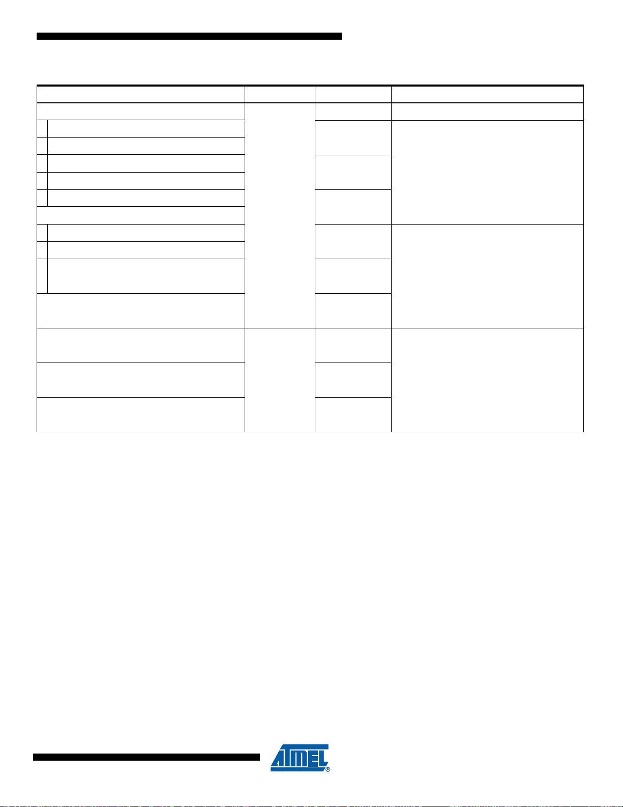
SAM4S Series [Preliminary]
Table 11-11. Faults (Continued)
Fault Handler Bit Name Fault Status Register
MPU or default memory map mismatch:
on instruction access IACCVIOL
on data access DACCVIOL
during exception stacking MSTKERR
during exception unstacking MUNSKERR
during lazy floating-point state preservation MLSPERR
Bus error:
during exception stacking STKERR
during exception unstacking UNSTKERR
during instruction prefetch IBUSERR
during lazy floating-point state preservation LSPERR
Precise data bus error PRECISERR
Imprecise data bus error IMPRECISERR
Memory
management
fault
Bus fault
--
(2)
“MMFSR: Memory Management Fault
Status Subregister”
--
“BFSR: Bus Fault Status Subregister”
Attempt to access a coprocessor
Undefined instruction UNDEFINSTR
Attempt to enter an invalid instruction set state
Invalid EXC_RETURN value INVPC
Illegal unaligned load or store UNALIGNED
Divide By 0 DIVBYZERO
Notes: 1. Occurs on an access to an XN region even if the processor does not include an MPU or the MPU is disabled.
2. Attempt to use an instruction set other than the Thumb instruction set, or return to a non load/store-multiple instruction with
ICI continuation.
(1)
Usage fault
NOCP
INVSTATE
“UFSR: Usage Fault Status Subregister”
Fault Escalation and Hard Faults
All faults exceptions except for hard fault have co nfigurab le except ion priorit y, se e “System Han-
dler Priority Registers” . The software can disable the execution of the handlers for these faults,
see “System Handler Control and State Register” .
Usually, the exception priority, together with the values of th e exception mask registers , deter-
mines whether the processor enters the fault handler, and whether a fault handler can preempt
another fault handler, as described in “Exception Model” .
In some situations, a fault with configurable priority is treated as a hard fault. This is called prior-
ity escalation, and the fault is described as escalated to hard fault. Escalation to hard fault
occurs when:
11100B–ATARM–31-Jul-12
• A fault handler causes the same kind of fault as the one it is servicing. This escalation to hard
fault occurs because a fault handler cannot preempt itself; it must have the same priority as
the current priority level.
• A fault handler causes a fault with the same o r lo wer priority as the fault it is servicing. This is
because the handler for the new fault cannot preempt the currently executing fault handler.
• An exception handler causes a fault for which the priority is the same as or lower than the
currently executing exception.
77
Page 78

• A fault occurs and the handler for that fault is not enabled.
If a bus fault occurs during a stack push when entering a bus fault handle r, the bus fault doe s not
escalate to a hard fault. This means that if a corrupted stack causes a fault, the fault handler
executes even though the stack push for the handler failed. The fault han dler operates but the
stack contents are corrupted.
Note: Only Reset and NMI can preempt the fixed priority hard fault. A hard fault can preempt any excep-
tion other than Reset, NMI, or another hard fault.
Fault Status Registers and Fault Address Registers
The fault status registers indicate the cause of a fault. For bus faults and memory management
faults, the fault address register indicates the address accessed by the op eration that caused
the fault, as shown in Table 11-12.
Table 11-12. Fault Status and Fault Address Registers
Lockup
Status Register
Handler
Hard fault SCB_HFSR - “Hard Fault Status Register”
Memory
management fault
Bus fault BFSR SCB_BFAR
Usage fault UFSR -
Name
MMFSR SCB_MMFAR
Address
Register Name Register Description
“MMFSR: Memory Management Fault
Status Subregister”
“MemManage Fault Address Register”
“BFSR: Bus Fault Status Subregister”
“Bus Fault Address Register”
“UFSR: Usage Fault Status
Subregister”
The processor enters a lockup state if a hard fault occurs when executing the NMI or hard fault
handlers. When the processor is in lockup state, it does not execute any instructions. The processor remains in lockup state until either:
• it is reset
• an NMI occurs
• it is halted by a debugger.
Note: If the lockup state occurs from the NMI handler, a subsequent NMI does not cause the processor
to leave the lockup state.
78
SAM4S Series [Preliminary]
11100B–ATARM–31-Jul-12
Page 79

11.5 Power Management
The Cortex-M4 processor sleep modes reduce the power consumption:
• Sleep mode stops the processor clock
• Deep sleep mode stops the system clock and switches off the PLL and flash memory.
The SLEEPDEEP bit of the SCR selects which sleep mode is used; see “System Control Regis-
ter” .
This section describes the mechanisms for entering sleep mode, and the conditions for waking
up from sleep mode.
11.5.1 Entering Sleep Mode
This section describes the mechanisms software can use to put the pro cessor into sleep mode.
The system can generate spurious wakeup events, for example a debug oper ation wakes up the
processor. Therefore, the software must be able to put the processor back int o sleep mo de aft er
such an event. A program might have an idle loop to put the processor back to sleep mode.
11.5.1.1 Wait for Interrupt
The wait for interrupt instruction, WFI, causes immediate e ntry to sleep mod e. When the processor executes a WFI instruction it stops executing instructions and enters sleep mode. See “WFI”
for more information.
SAM4S Series [Preliminary]
11.5.1.2 Wait For Event
The wait for event instruction, WFE, causes entry to sleep mode conditional on the value of an
one-bit event register. When the processor executes a WFE instruction, it checks this register:
• if the register is 0, the processor stops executing instructions and enters sleep mode
• if the register is 1, the processor clears the register to 0 and contin ue s execut ing instructions
without entering sleep mode.
See “WFE” for more information.
11.5.1.3 Sleep-On-Exit
If the SLEEPONEXIT bit of the SCR is set to 1 when the processor completes the execution of
an exception handler, it returns to Thread mode and immediately enters sleep mode. Use this
mechanism in applications that only require the processor to run when an exception occurs.
11.5.2 Wakeup From Sleep Mode
The conditions for the processor to wake up depend on the mechanism that cause it to enter
sleep mode.
11.5.2.1 Wakeup from WFI or Sleep-on-exit
Normally, the processor wakes up only when it detects an exception with sufficient priority to
cause exception entry.
Some embedded systems might have to execute system restore tasks after the processor
wakes up, and before it executes an interrupt handler. To achieve this, set the PRIMASK bit to 1
and the FAULTMASK bit to 0. If an interrupt arrives that is enabled and has a higher priority than
the current exception priority, the processor wa kes up b ut does not execute th e inte rrupt h andler
until the processor sets PRIMASK to zero. For more information about PRIMASK and FAULTMASK, see “Exception Mask Registers” .
11100B–ATARM–31-Jul-12
79
Page 80

11.5.2.2 Wakeup from WFE
The processor wakes up if:
• it detects an exception with sufficient priority to cause an exception entry
• it detects an external event signal. See “External Event Input”
• in a multiprocessor system, another processor in the system executes an SEV instruction.
In addition, if the SEVONPEND bit in the SCR is set to 1, any new pending interrupt triggers an
event and wakes up the processor, even if the interrupt is disabled or has insufficient priority to
cause an exception entry. For more informatio n ab o ut th e SCR, see “System Control Register” .
11.5.2.3 External Event Input
The processor provides an external event input signal. Periphera ls can drive this signal, eit her to
wake the processor from WFE, or to set the internal WFE event register to 1 to indicate that the
processor must not enter sleep mode on a later WFE instru ction. See “Wait For Event” for more
information.
11.5.3 Power Management Programming Hints
ISO/IEC C cannot directly generate the WF I a nd WFE instr u ctio ns . Th e C MSIS pr ovides the following functions for these instructions:
void __WFE(void) // Wait for Event
void __WFE(void) // Wait for Interrupt
80
SAM4S Series [Preliminary]
11100B–ATARM–31-Jul-12
Page 81

SAM4S Series [Preliminary]
11.6 Cortex-M4 Instruction Set
11.6.1 Instruction Set Summary
The processor implements a version of the Thumb instruction set. Table 11-13 lists the supported instructions.
• angle brackets, <>, enclose alternative forms of the operand
• braces, {}, enclose optional operands
• the Operands column is not exhaustive
• Op2 is a flexible second operand that can be either a register or a constant
• most instructions can use an optional condition code suffix.
For more information on the instructions and operands, see the instruction descriptions.
Table 11-13. Cortex -M 4 In str uc tio ns
Mnemonic Operands Description Flags
ADC, ADCS {Rd,} Rn, Op2 Add with Carry N,Z,C,V
ADD, ADDS {Rd,} Rn, Op2 Add N,Z,C,V
ADD, ADDW {Rd,} Rn, #imm12 Add N,Z,C,V
ADR Rd, label Load PC-relative address AND, ANDS {Rd,} Rn, Op2 Logical AND N,Z,C
ASR, ASRS Rd, Rm, <Rs|#n> Arithmetic Shift Right N,Z,C
B label Branch BFC Rd, #lsb, #width Bit Field Clear BFI Rd, Rn, #lsb, #width Bit Field Insert BIC, BICS {Rd,} Rn, Op2 Bit Clear N,Z,C
BKPT #imm Breakpoint BL label Branch with Link BLX Rm Branch indirect with Link BX Rm Branch indirect CBNZ Rn, label Compare and Branch if Non Zero CBZ Rn, label Compare and Branch if Zero CLREX - Clear Exclusive CLZ Rd, Rm Count leading zeros CMN Rn, Op2 Compare Negative N,Z,C,V
CMP Rn, Op2 Compare N,Z,C,V
CPSID i Change Processor State, Disable Interrupts CPSIE i Change Processor State, Enable Interrupts DMB - Data Memory Barrier DSB - Data Synchro nization Barrier EOR, EORS {Rd,} Rn, Op2 Exclusive OR N,Z,C
ISB - Instruction Synchronization Barrier -
11100B–ATARM–31-Jul-12
81
Page 82

Table 11-13. Cortex -M 4 In str uc tio ns (Co n tin ue d)
Mnemonic Operands Description Flags
IT - If-Then condition block LDM Rn{!}, reglist Load Multiple registers, increment after LDMDB, LDMEA Rn{!}, reglist Load Multiple registers, decrement before LDMFD, LDMIA Rn{!}, reglist Load Multiple registers, increment after LDR Rt, [Rn, #offset] Load Register with word LDRB, LDRBT Rt, [Rn, #offset] Load Register with byte LDRD Rt, Rt2, [Rn, #offset] Load Register with two bytes LDREX Rt, [Rn, #offset] Load Register Exclusive LDREXB Rt, [Rn] Load Register Exclusive with byte LDREXH Rt, [Rn] Load Register Exclusive with halfword LDRH, LDRHT Rt, [Rn, #offset] Load Register with halfword LDRSB, DRSBT Rt, [Rn, #offset] Load Register with signed byte LDRSH, LDRSHT Rt, [Rn, #offset] Load Register with signed halfword LDRT Rt, [Rn, #offset] Load Register with word LSL, LSLS Rd, Rm, <Rs|#n> Logical Shift Left N,Z,C
LSR, LSRS Rd, Rm, <Rs|#n> Logical Shift Right N,Z,C
MLA Rd, Rn, Rm, Ra Multiply with Accumulate, 32-bit result MLS Rd, Rn, Rm, Ra Multiply and Subtract, 32-bit result MOV, MOVS Rd, Op2 Move N,Z,C
MOVT Rd, #imm16 Move Top MOVW, MOV Rd, #imm16 Move 16-bit constant N,Z,C
MRS Rd, spec_reg Move from special register to general register MSR spec_reg, Rm Move from general register to special register N,Z,C,V
MUL, MULS {Rd,} Rn, Rm Multiply, 32-bit result N,Z
MVN, MVNS Rd, Op2 Move NOT N,Z,C
NOP - No Operation ORN, ORNS {Rd,} Rn, Op2 Logical OR NOT N,Z,C
ORR, ORRS {Rd,} Rn, Op2 Logical OR N,Z,C
PKHTB, PKHBT {Rd,} Rn, Rm, Op2 Pack Halfword POP r eglist Pop registers from stack PUSH reglist P ush registers onto stack QADD {Rd,} Rn, Rm Saturating double and Add Q
QADD16 {Rd,} Rn, Rm Saturating Add 16 QADD8 {Rd,} Rn, Rm Saturating Add 8 QASX {Rd,} Rn, Rm Saturating Add and Subtract with Exchange QDADD {Rd,} Rn, Rm Saturating Add Q
82
SAM4S Series [Preliminary]
11100B–ATARM–31-Jul-12
Page 83

SAM4S Series [Preliminary]
Table 11-13. Cortex -M 4 In str uc tio ns (Co n tin ue d)
Mnemonic Operands Description Flags
QDSUB {Rd,} Rn, Rm Saturating double and Subtract Q
QSAX {Rd,} Rn, Rm Saturating Subtract and Add with Exchange QSUB {Rd,} Rn, Rm Saturating Subtract Q
QSUB16 {Rd,} Rn, Rm Saturating Subtract 16 QSUB8 {Rd,} Rn, Rm Saturating Subtract 8 RBIT Rd, Rn Reverse Bits REV Rd, Rn Reverse byte order in a word REV16 Rd, Rn Reverse byte order in each halfword REVSH Rd, Rn Reverse byte order in bottom halfword and sign extend ROR, RORS Rd, Rm, <Rs|#n> Rotate Right N,Z,C
RRX, RRXS Rd, Rm Rotate Right with Extend N,Z,C
RSB, RSBS {Rd,} Rn, Op2 Reverse Subtract N,Z,C,V
SADD16 {Rd,} Rn, Rm Signed Add 16 GE
SADD8 {Rd,} Rn, Rm Signed Add 8 and Subtract with Exchange GE
SASX {Rd,} Rn, Rm Signed Add GE
SBC, SBCS {Rd,} Rn, Op2 Subtract with Carry N,Z,C,V
SBFX Rd, Rn, #lsb, #width Signed Bit Field Extract SDIV {Rd,} Rn, Rm Signed Divide -
SEL {Rd,} Rn, Rm Select bytes SEV - Send Event SHADD16 {Rd,} Rn, Rm Signed Halving Add 16 -
SHADD8 {Rd,} Rn, Rm Signed Halving Add 8 SHASX {Rd,} Rn, Rm Signed Halv ing Add and Subtract with Exchange SHSAX {Rd,} Rn, Rm Signed Halv ing Subtract and Add with Exchange SHSUB16 {Rd,} Rn, Rm Signed Halving Subtract 16 SHSUB8 {Rd,} Rn, Rm Signed Halving Subtract 8 SMLABB, SMLABT,
SMLATB, SMLATT
SMLAD, SMLADX Rd, Rn, Rm, Ra Signed Multiply Accumulate Dual Q
SMLAL RdLo, RdHi, Rn, Rm Signed Multiply with Accumulate (32 x 32 + 64), 64-bit result SMLALBB, SMLALBT,
SMLALTB, SMLALTT
SMLALD, SMLALDX RdLo, RdHi, Rn, Rm Signed Multiply Accumulate Long Dual SMLAWB, SMLAWT Rd, Rn, Rm, Ra Signed Multiply Accumulate, word by halfword Q
SMLSD Rd, Rn, Rm, Ra Signed Multiply Subtract Dual Q
SMLSLD RdLo, RdHi, Rn, Rm Signed Multiply Subtract Long Dual
SMMLA Rd, Rn, Rm, Ra Signed Most significant word Multiply Accumulate SMMLS, SMMLR Rd, Rn, Rm, Ra Signed Most significant word Multiply Subtract SMMUL, SMMULR {Rd,} Rn, Rm Signed Most significant word Multiply SMUAD {Rd,} Rn, Rm Signed dual Multiply Add Q
Rd, Rn, Rm, Ra Signed Multiply Accumulate Long (halfwords) Q
RdLo, RdHi, Rn, Rm Signed Multiply Accumulate Long, halfwords -
11100B–ATARM–31-Jul-12
83
Page 84

Table 11-13. Cortex -M 4 In str uc tio ns (Co n tin ue d)
Mnemonic Operands Description Flags
SMULBB, SMULBT
SMULTB, SMULTT
SMULL RdLo, RdHi, Rn, Rm Signed Multiply (32 x 32), 64-bit result SMULWB, SMULWT {Rd,} Rn, Rm Signed Multiply word by halfword -
SMUSD, SMUSDX {Rd,} Rn, Rm Signed dual Multiply Subtract SSAT Rd, #n, Rm {,shift #s} Signed Saturate Q
SSAT16 Rd, #n, Rm Signed Saturate 16 Q
SSAX {Rd,} Rn, Rm Signed Subtract and Add with Exchange GE
SSUB16 {Rd,} Rn, Rm Signed Subtract 16 SSUB8 {Rd,} Rn, Rm Signed Subtract 8 -
STM Rn{!}, reglist Store Multiple registers, increment after STMDB, STMEA Rn{!}, reglist Store Multiple registers, decrement before STMFD, STMIA Rn{!}, reglist Store Multiple registers, increment after STR Rt, [Rn, #offset] Store Register word STRB, STRBT Rt, [Rn, #offset] Store Register byte STRD Rt, Rt2, [Rn, #offset] Store Register two words STREX Rd, Rt, [Rn, #offset] Store Register Exclusive STREXB Rd, Rt, [Rn] Store Register Exclusive byte -
{Rd,} Rn, Rm Signed Multiply (halfwords) -
STREXH Rd, Rt, [Rn] Store Register Exclusive halfword STRH, STRHT Rt, [Rn, #offset] Store Register halfword STRT Rt, [Rn, #offset] Store Register word SUB, SUBS {Rd,} Rn, Op2 Subtract N,Z,C,V
SUB, SUBW {Rd,} Rn, #imm12 Subtract N,Z,C,V
SVC #imm Supervisor Call -
SXTAB {Rd,} Rn, Rm,{,ROR #} Extend 8 bits to 32 and add SXTAB16 {Rd,} Rn, Rm,{,ROR #} Dual extend 8 bits to 16 and add SXTAH {Rd,} Rn, Rm,{,ROR #} Extend 16 bits to 32 and add SXTB16 {Rd,} Rm {,ROR #n} Signed Extend Byte 16 -
SXTB {Rd,} Rm {,ROR #n} Sign extend a byte SXTH {Rd,} Rm {,ROR #n} Sign extend a halfword TBB [Rn, Rm] Table Branch Byte TBH [Rn, Rm, LSL #1] Table Branch Halfword TEQ Rn, Op2 Test Equivalence N,Z,C
TST Rn, Op2 Test N,Z,C
UADD16 {Rd,} Rn, Rm Unsigned Add 16 GE
UADD8 {Rd,} Rn, Rm Unsigned Add 8 GE
USAX {Rd,} Rn, Rm Unsigned Subtract and Add with Exchange GE
UHADD16 {Rd,} Rn, Rm Unsigned Halving Add 16 UHADD8 {Rd,} Rn, Rm Unsigned Halving Add 8 UHASX {Rd,} Rn, Rm Unsigned Halving Add and Subtract with Exchange UHSAX {Rd,} Rn, Rm Unsigned Halving Subtract and Add with Exchange -
84
SAM4S Series [Preliminary]
11100B–ATARM–31-Jul-12
Page 85

SAM4S Series [Preliminary]
Table 11-13. Cortex -M 4 In str uc tio ns (Co n tin ue d)
Mnemonic Operands Description Flags
UHSUB16 {Rd,} Rn, Rm Unsigned Halving Subtract 16 UHSUB8 {Rd,} Rn, Rm Unsigned Halving Subtract 8 -
UBFX Rd, Rn, #lsb, #width Unsigned Bit Field Extract UDIV {Rd,} Rn, Rm Unsigned Divide -
UMAAL RdLo, RdHi, Rn, Rm Unsigned Multiply Accumulate Accumulate Long (32 x 32 + 32 +32),
64-bit result
UMLAL RdLo, RdHi, Rn, Rm
UMULL RdLo, RdHi, Rn, Rm Unsigned Multiply (32 x 32), 64-bit result UQADD16 {Rd,} Rn, Rm Unsigned Saturating Add 16 -
UQADD8 {Rd,} Rn, Rm Unsigned Saturating Add 8 UQASX {Rd,} Rn, Rm Unsigned Saturating Add and Subtract with Exchange UQSAX {Rd,} Rn, Rm Unsigned Saturating Subtract and Add with Exchange UQSUB16 {Rd,} Rn, Rm Unsigned Saturating Subtract 16 UQSUB8 {Rd,} Rn, Rm Unsigned Saturating Subtract 8 USAD8 {Rd,} Rn, Rm Unsigned Sum of Absolute Differences USADA8 {Rd,} Rn, Rm, Ra Un signed Sum of Absolute Differences and Accumulate -
USAT Rd, #n, Rm {,shift #s} Unsigned Saturate Q
USAT16 Rd, #n, Rm Unsigned Saturate 16 Q
UASX {Rd,} Rn, Rm Unsigned Add and Subtract with Exchange GE
USUB16 {Rd,} Rn, Rm Unsigned Subtract 16 GE
USUB8 {Rd,} Rn, Rm Unsigned Subtract 8 GE
UXTAB {Rd,} Rn, Rm,{,ROR #} Rotate, extend 8 bits to 32 and Add UXTAB16 {Rd,} Rn, Rm,{,ROR #} Rotate, dual extend 8 bits to 16 and Add UXTAH {Rd,} Rn, Rm,{,ROR #} Rotate, unsigned extend and Add Halfword -
UXTB {Rd,} Rm {,ROR #n} Zero extend a byte UXTB16 {Rd,} Rm {,ROR #n} Unsigned Extend Byte 16 UXTH {Rd,} Rm {,ROR #n} Zero extend a halfword -
WFE - Wait For Event WFI - Wait For Interrupt -
Unsigned Multiply with Accumulate
(32 x 32 + 64), 64-bit result
-
-
11.6.2 CMSIS Functions
ISO/IEC cannot directly access some Cortex-M4 instructions. This section describes intrinsic
functions that can generate these instructions, provided by the CMIS and that might be provided
by a C compiler. If a C compiler does not support an appropriat e intrinsic function , the user might
have to use inline assembler to access some instructions.
11100B–ATARM–31-Jul-12
85
Page 86
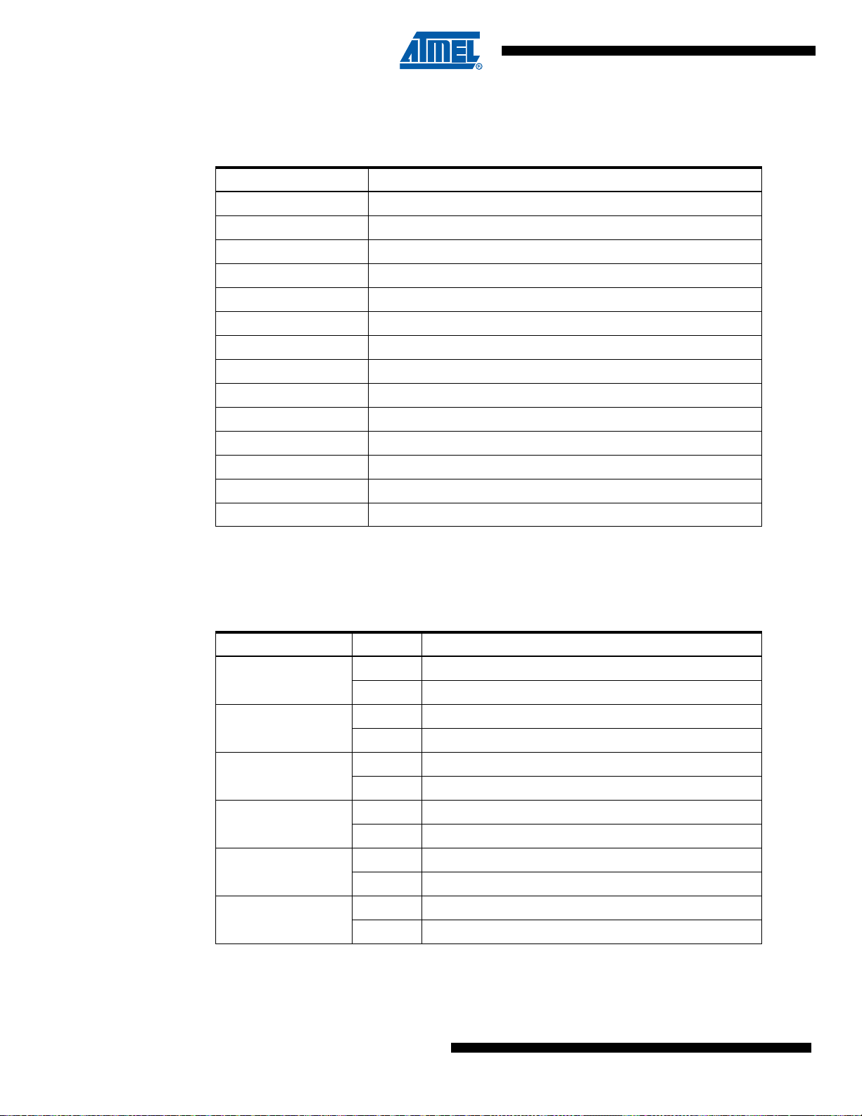
The CMSIS provides the following intrinsic functions to generate instructions that ISO/IEC C
code cannot directly access:
Table 11-14. CMSIS Functions to Generate some Cortex-M4 Instructions
Instruction CMSIS Function
CPSIE I void __enable_irq(void)
CPSID I void __disable_irq(void)
CPSIE F void __enable_fault_irq(void)
CPSID F void __disable_fault_irq(void)
ISB void __ISB(void)
DSB void __DSB(void)
DMB void __DMB(void)
REV uint32_t __REV(uint32_t int value)
REV16 uint32_t __REV16(uint32_t int value)
REVSH uint32_t __REVSH(uint32_t int value)
RBIT uint32_t __RBIT(uint32_t int value)
SEV void __SEV(void)
WFE void __WFE(void)
WFI void __WFI(void)
The CMSIS also provides a number of functions for accessing the special registers using MRS
and MSR instructions:
Table 11-15. CMSIS Intrinsic Functions to Access the Special Registers
Special Register Access CMSIS Function
PRIMASK
FAULTMASK
BASEPRI
CONTROL
MSP
PSP
Read uint3 2_t __get_PRIMASK (void)
Write void __set_PRIMASK (uint32_t value)
Read uint3 2_t __get_FAULTMASK (void)
Write void __set_FAULTMASK (uint32_t value)
Read uint32_t __get_BASEPRI (void)
Write void __set_BASEPRI (uint32_t value)
Read uint3 2_t __get_CONTROL (void)
Write void __set_CONTROL (uint32_t value)
Read uint3 2_t __get_MSP (void)
Write void __set_MSP (uint32_t TopOfMainStack)
Read uint3 2_t __get_PSP (void)
Write void __set_PSP (uint32_t TopOfProcStack)
86
SAM4S Series [Preliminary]
11100B–ATARM–31-Jul-12
Page 87

11.6.3 Instruction Descriptions
11.6.3.1 Operands
An instruction operand can be an ARM register, a constant, or another instruction-specific
parameter. Instructions act on the operands and often store the result in a destination register.
When there is a destination register in the instruction, it is usually specifie d before the operands.
Operands in some instructions are flexible, can either be a register or a constant. See “Flexible
Second Operand” .
11.6.3.2 Restrictions when Using PC or SP
Many instructions have restrictio ns on whet her the Program Counter (PC) or Stack Pointer (SP)
for the operands or destination register can be used. See instruction descriptions for more
information.
Note: Bit[0] of any address written to the PC with a BX, BLX, LDM, LDR, or POP instruction must be 1
for correct execution, because this bit indicates the required instruction set, and the Cortex-M4
processor only supports Thumb instructions.
11.6.3.3 Flexible Second Operand
Many general data processing instructions have a flexible second operand. This is shown as
Operand2 in the descriptions of the syntax of each instruction.
SAM4S Series [Preliminary]
Constant
Operand2 can be a:
• “Constant”
• “Register with Optional Shift”
Specify an Operand2 constant in the form:
#constant
where constant can be:
• any constant that can be produced by shifting an 8-bit value left by any number of bits within
a 32-bit word
• any constant of the form 0x00XY00XY
• any constant of the form 0xXY00XY00
• any constant of the form 0xXYXYXYXY.
Note: In the constants shown above, X and Y are hexadecimal digits.
In addition, in a small number of instructions, constant can take a wider range of values.
These are described in the individual instruction descriptions.
When an Operand2 constant is used with the instructions MOVS, MVNS, ANDS, ORRS, ORNS,
EORS, BICS, TEQ or TST, the carry flag is updated to bit[31] of the constant, if the constant is
greater than 255 and can be produced by shifting an 8-bit value. These inst ructio ns do not aff ect
the carry flag if Operand2 is any other constant.
Instruction Substitution
11100B–ATARM–31-Jul-12
The assembler might be able to produce an equivalent instruct ion in cases wher e the u ser specifies a constant that is not permitted. For example, an assembler might assemble the instruction
CMP
Rd
, #0xFFFFFFFE as the equivalent instruction CMN Rd, #0x2.
87
Page 88

Register with Optional Shift
Specify an Operand2 register in the form:
where:
Rm is the register holding the data for the second operand.
shift is an optional shift to be applied to Rm. It can be one of:
If the user omits the shift, or specifies LSL #0, the instruction uses the value in Rm.
If the user specifies a shift, the shift is applied to the value in Rm, and the resulting 32-bit value
is used by the instruction. However, the contents in the register Rm remains unchanged. Specifying a register with shift also updates the carry flag when used with certain instructions. For
information on the shift operations and how they affect the ca rry flag, see “Flexible Second
Operand” .
Rm {, shift}
ASR #n arithmetic shift right n bits, 1 ≤ n ≤ 32.
LSL #n logical shift left n bits, 1 ≤ n ≤ 31.
LSR #n logical shift right n bits, 1 ≤ n ≤ 32.
ROR #n rotate right n bits, 1 ≤ n ≤ 31.
RRX rotate right one bit, with extend.
- if omitted, no shift occurs, equivalent to LSL #0.
11.6.3.4 Shift Operations
Register shift operations move the bits in a register lef t or r igh t b y a specified numb er of bits , the
shift length. Register shift can be performed:
The permitted shift lengths depend on th e shift type and the instruction. I f the shif t lengt h is 0, no
shift occurs. Register shift operations update t he carry flag except when the specified shif t length
is 0. The following sub-sections describe the various shift operations and how they affect the
carry flag. In these descriptions, Rm is the register containing the value to be shifted, and n is
the shift length.
ASR
Arithmetic shift right by n bits moves the left-hand 32-n bits of the register, Rm, to the right by n
places, into the right-hand 32-n bits of the result. And it copies the original bit[31] of the register
into the left-hand n bits of the result. See Figure 11-7
Th
being rounded towards negative-infinity.
When the instruction is ASRS or when ASR #n is used in Operand2 with the instructions MOVS,
MVNS, ANDS, ORRS, ORNS, EORS, BICS, TEQ or TST, the carry flag is updated to the last bit
shifted out, bit[n-1], of the register Rm.
• Directly by the instructions ASR, LSR, LSL, ROR, and RRX, and the result is written to a
destination register
• During the calculation of Operand2 by the instructions that specify the second operand as a
register with shift. See “Flexible Second Operand” . The result is used by the instruction.
.
n
e ASR #n
operation can be used to divide the value in the register Rm by 2
, with the result
88
•If n is 32 or more, then all the bits in the result are set to the value of bit[31] of Rm.
•If n is 32 or more and the carry flag is updated, it is updated to the value of bit[31] of Rm.
SAM4S Series [Preliminary]
11100B–ATARM–31-Jul-12
Page 89
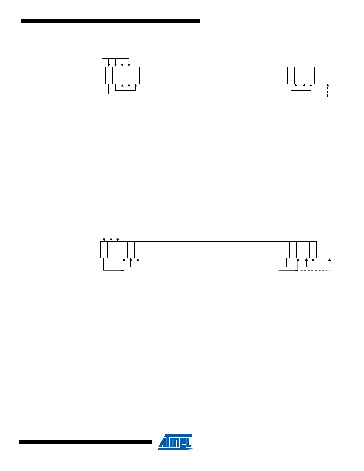
LSR
Carry
Flag
031 5 4 3 2 1
Carry
Flag
031 5 4 3 2 1
00
0
SAM4S Series [Preliminary]
Figure 11-7. ASR #3
Logical shift right by n bits moves the left-hand 32-n bits of the register Rm, to the right by n
places, into the right-hand 32-n bits of the re sult. And it sets the left-ha nd n bit s of the r esult to 0.
See Figure 11-8.
n
The LSR #n operation can be used to divide the value in the register Rm by 2
regarded as an unsigned integer.
When the instruction is LSRS or when LSR #n is used in Operand2 with the instructions MOVS,
MVNS, ANDS, ORRS, ORNS, EORS, BICS, TEQ or TST, the carry flag is updated to the last bit
shifted out, bit[n-1], of the register Rm.
•If n is 32 or more, then all the bits in the result are cleared to 0.
•If n is 33 or more and the carry flag is updated, it is updated to 0.
, if the value is
LSL
Figure 11-8. LSR #3
Logical shift left by n bits moves the right-hand 32-n bits of the register Rm, to the left by n
places, into the left-hand 32-n bits of the result. And it sets the right- hand n bit s of the result to 0.
See Figure 11-9.
The LSL #n operation can be used to multiply the value in the register Rm by 2
n
, if the value is
regarded as an unsigned integer or a two’s complement signed integer. Overflow can occur
without warning.
When the instruction is LSLS or when LSL #n, with non-zero n, is used in Operand2 with the
instructions MOVS, MVNS, ANDS, ORRS, ORNS, EORS, BICS, TEQ or TST, the carry flag is
updated to the last bit shifted out, bit[32-n], of the register Rm. These instructions do not affect
the carry flag when used with LSL #0.
•If n is 32 or more, then all the bits in the result are cleared to 0.
•If n is 33 or more and the carry flag is updated, it is updated to 0.
11100B–ATARM–31-Jul-12
89
Page 90
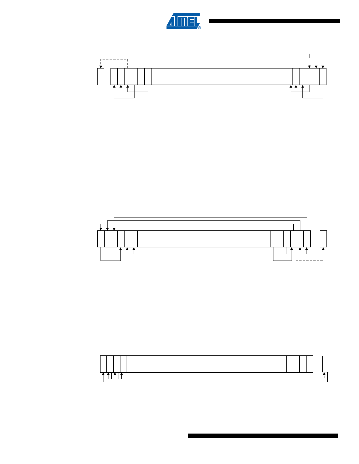
ROR
031 5 4 3 2 1
Carry
Flag
00
0
Carry
Flag
031 5 4 3 2 1
30
Carry
Flag
031 1
Figure 11-9. LSL #3
Rotate right by n bits moves the left-hand 32-n bits of the register Rm, to the right by n places,
into the right-hand 32-n bits of the result. And it moves the right-hand n bits of the register into
the left-hand n bits of the result. See Figure 11-10.
When the instruction is RORS or when ROR #n is used in Operand2 with the instructions MOVS,
MVNS, ANDS, ORRS, ORNS, EORS, BICS, TEQ or TST, the carry flag is updated to the last bit
rotation, bit[n-1], of the register Rm.
•If n is 32, then the value of the result is same as the value in Rm, and if the carry flag is
updated, it is updated to bit[31] of Rm.
• ROR with shift length, n, more than 32 is the same as ROR with shift length n-32.
Figure 11-10. ROR #3
90
RRX
Rotate right with extend moves the bits of the register Rm to the right by one bit. And it copies
the carry flag into bit[31] of the result. See Figure 11-11.
When the instruction is RRXS or when RRX is used in Operand2 with the instructions MOVS,
MVNS, ANDS, ORRS, ORNS, EORS, BICS, TEQ or TST, the carry flag is updated to bit[0] of
the register Rm.
Figure 11-11. RRX
SAM4S Series [Preliminary]
11100B–ATARM–31-Jul-12
Page 91

11.6.3.5 Address Alignment
An aligned access is an operation where a word-aligned address is used for a word, dual word,
or multiple word access, or where a halfword-aligned address is used for a halfword access.
Byte accesses are always aligned.
The Cortex-M4 processor supports unaligned access only for the following instructions:
• LDR, LDRT
• LDRH, LDRHT
• LDRSH, LDRSHT
•STR, STRT
• STRH, STRHT
All other load and store instructions generate a usage fault exception if they perform an
unaligned access, and therefore their accesses must be address-aligned. For more information
about usage faults, see “Fault Handling” .
Unaligned accesses are usually slower than aligned accesses. In addition, some memory
regions might not support unaligned accesses. Therefore, ARM recommends that programmers
ensure that accesses are aligned. To avoid accidental generation of unaligned accesses, use
the UNALIGN_TRP bit in the Configuration and Control Register to trap all unaligned accesses,
see “Configuration and Control Register” .
SAM4S Series [Preliminary]
11.6.3.6 PC-relative Expressions
A PC-relative expression or label is a symbol that represents the address of an instruction or literal data. It is represented in the instruction as the PC value plus or min us a numeric offset. The
assembler calculates the required offset from the label and the address of the current instruction. If the offset is too big, the assembler produces an error.
• For B, BL, CBNZ, and CBZ instructions, the value of the PC is the address of the current
instruction plus 4 bytes.
• For all other instructions that use labels, the value of the PC is the address of t he current
instruction plus 4 bytes, with bit[1] of the result cleared to 0 to make it word-aligned.
• Your assembler might permit other syntaxes for PC-relative expr essions , such as a label plus
or minus a number, or an expression of the form [PC, #number].
11.6.3.7 Conditional Execution Most data processing instructions can optionally update the condition flags in the Application
Program Status Register (APSR) according to the result of the operation, see “Application Pro-
gram Status Register” . Some instructions update all flags, and some only update a subset. If a
flag is not updated, the original value is preserved. See the instruction descriptions for the flags
they affect.
An instruction can be executed conditionally, ba sed on the condition flags set in another instruction, either:
• immediately after the instruction that updated the flags
• after any number of intervening instructions that have not updated the flags.
Conditional execution is available by using conditional branches or by adding condition code
suffixes to instructions. See Table 11-16 for a list of the suffixes to add to instructions to make
them conditional instructions. The condition code suffix enables the processor t o test a condition
based on the flags. If the condition test of a conditiona l instr u ctio n fa ils, the inst ru ctio n:
11100B–ATARM–31-Jul-12
91
Page 92

Condition Flags
• does not execute
• does not write any value to its destination register
• does not affect any of the flags
• does not generate any exception.
Conditional instructions, except for conditional branches, must be inside an If-Then instruction
block. See “” for more information and restrictions when using the IT instruction. Depending on
the vendor, the assembler might automatically insert an IT instruction if there are conditional
instructions outside the IT block.
The CBZ and CBNZ instructions are used to compare the value of a register against zero and
branch on the result.
This section describes:
• “Condition Flags”
• “Condition Code Suffixes” .
The APSR contains the following condition flags:
N Set to 1 when the result of the operation was negative, cleared to 0 otherwise.
Z Set to 1 when the result of the operation was zero, cleared to 0 otherwise.
C Set to 1 when the operation resulted in a carry, cleared to 0 otherwise.
Condition Code Suffixes
V Set to 1 when the operation caused overflow, cleared to 0 other wise.
For more information about the APSR, see “Program Status Register” .
A carry occurs:
• if the result of an addition is greater than or equal to 2
• if the result of a subtraction is positive or zero
• as the result of an inline barrel shifter operation in a move or logical instruction.
An overflow occurs when the sign of the result, in bit[31], does not match the sign of the result,
had the operation been performed at infinite precision, for example:
• if adding two negative values results in a positive value
• if adding two positive values results in a negative value
• if subtracting a positive value from a negative value generates a positive value
• if subtracting a negative value from a positive value generates a negative value.
The Compare operations are identical to subtracting, for CMP, or adding, for CMN, except that
the result is discarded. See the instruction descriptions for mor e information.
Note: Most instructions update the status flags only if the S suffix is specified. See the instruction
descriptions for more information.
The instructions that can be conditional have an optional condition code, shown in syntax
descriptions as {cond}. Conditional execution requires a preceding IT instruction. An instruction
with a condition code is only executed if the condition code flags in the APSR meet the specified
condition. Table 11-16 shows the condition codes to use.
32
92
SAM4S Series [Preliminary]
11100B–ATARM–31-Jul-12
Page 93
SAM4S Series [Preliminary]
A conditional execution can be used with the IT instruction to reduce the number of branch
instructions in code.
Table 11-16 also shows the relationship between condition cod e su ff ixes an d th e N, Z , C, an d V
flags.
Table 11-16. Condition Code Suffixes
Suffix Flags Meaning
EQ Z = 1 Equal
NE Z = 0 Not equal
Absolute Value
CS or
HS
CC or
LO
MI N = 1 Negative
PL N = 0 Positive or zero
VS V = 1 Overflow
VC V = 0 No overflow
HI C = 1 and Z = 0 Higher, unsigned >
LS C = 0 or Z = 1 Lower or same, unsigned ≤
GE N = V Greater than or equal, signed ≥
LT N ! = V Less than, signed <
GT Z = 0 and N = V Greater than, signed >
LE Z = 1 and N != V Less than or equal, signe d ≤
AL
C = 1 Higher or same, unsigned ≥
C = 0 Lower, unsigned <
Can have any
value
Always. This is the default when no suffix is
specified.
The example below shows the use of a conditional instruction to find the absolute value of a
number. R0 = ABS(R1).
MOVS R0, R1 ; R0 = R1, setting flags
IT MI ; IT instruction for the negative condition
RSBMI R0, R1, #0 ; If negative, R0 = -R1
Compare and Update Value
The example below shows the use of conditional instructions to update the value of R4 if the
signed values R0 is greater than R1 and R2 is greater than R3.
CMP R0, R1 ; Compare R0 and R1, setting flags
ITT GT ; IT instruction for the two GT conditions
CMPGT R2, R3 ; If 'greater than', compare R2 and R3, setting flags
MOVGT R4, R5 ; If still 'greater than', do R4 = R5
11.6.3.8 Instruction Width Selection
There are many instructions that can generate either a 16-bit encoding or a 32-bit encoding
depending on the operands and destination register specified. For some of these instructions,
11100B–ATARM–31-Jul-12
93
Page 94

the user can force a specific instruction size by using an instruction width suffix. The .W suffix
forces a 32-bit instruction encoding. The .N suffix forces a 16-bit instruction encoding.
If the user specifies an instruction width suffix and the assembler cannot generate an instruction
encoding of the requested width, it generates an error.
Note: In some cases, it might be necessary to specify the .W suffix, for example if the operand is the
label of an instruction or literal data, as in the case of branch instructions. This is because the
assembler might not automatically generate the right size encoding.
To use an instruction width suffix, place it immediately after the instruction mnemonic and condition code, if any. The example below shows instructions with the instruction width suffix.
BCS.W label ; creates a 32-bit instruction even for a short branch
ADDS.W R0, R0, R1 ; creates a 32-bit instruction even though the same
11.6.4 Memory Access Instructions
The table below shows the memory access instructions:
Table 11-17. Memory Access Instructions
Mnemonic Description
ADR Load PC-relative address
; operation can be done by a 16-bit instruction
CLREX Clear Exclusive
LDM{mode} Load Multi ple registers
LDR{type} Load Register using immediate offset
LDR{type} Load Register using register offset
LDR{type}T Load Register with unprivileged access
LDR Load Register using PC-relative address
LDRD Load Register Dual
LDREX{type} Load Register Exclusive
POP Pop registers from stack
PUSH Push registers onto stack
STM{mode} Store Multiple registers
STR{type} Store Register using immediate offset
STR{type} Store Register using register offset
STR{type}T Store Register with unprivileged access
STREX{type} Store Register Exclusive
94
SAM4S Series [Preliminary]
11100B–ATARM–31-Jul-12
Page 95

11.6.4.1 ADR
SAM4S Series [Preliminary]
Load PC-relative address.
Syntax
ADR{cond} Rd, label
where:
cond is an optional condition code, see “Conditional Execution” .
Rd is the destination register.
label is a PC-relative expression. See “PC-relative Expressions” .
Operation
ADR determines the address by adding an immediate value to the PC, and writes the result to
the destination register.
ADR produces position-independent code, because the address is PC-relative.
If ADR is used to generate a target address for a BX or BLX instruction, ensure that bit[0] of the
address generated is set to 1 for correct execution.
Values of label must be within the range of −4095 to +4095 from the address in the PC.
Note: The user might have to use the .W suffix to get the maximum offset range or to generate
addresses that are not word-aligned. See “Instruction Width Selection” .
Restrictions
Rd must not be SP and must not be PC.
Condition Flags
This instruction does not change the flags.
Examples
ADR R1, TextMessage ; Write address value of a location labelled as
; TextMessage to R1
11100B–ATARM–31-Jul-12
95
Page 96

11.6.4.2 LDR and STR, Immediate Offset
Load and Store with immediate offset, pre-indexed immediate offset, or post-indexed immediate
offset.
Syntax
op{type}{cond} Rt, [Rn {, #offset}] ; immediate offset
op{type}{cond} Rt, [Rn, #offset]! ; pre-indexed
op{type}{cond} Rt, [Rn], #offset ; post-indexed
opD{cond} Rt, Rt2, [Rn {, #offset}] ; immediate offset, two words
opD{cond} Rt, Rt2, [Rn, #offset]! ; pre-indexed, two words
opD{cond} Rt, Rt2, [Rn], #offset ; post-indexed, two words
where:
op is one of:
LDR Load Register.
STR Store Register.
type is one of:
B unsigned byte, zero extend to 32 bits on loads.
SB signed byte, sign extend to 32 bits (LDR only).
H unsigned halfword, zero extend to 32 bits on loads.
SH signed halfword, sign extend to 32 bits (LDR only).
- omit, for word.
cond is an optional condition code, see “Conditional Execution” .
Rt is the register to load or store.
Rn is the register on which the memory address is based.
offset is an offset from Rn. If offset is omitted, the address is the contents of Rn.
Rt2 is the additional register to load or store for two-word operations.
Operation
LDR instructions load one or two registers with a value from memory.
STR instructions store one or two register values to memory.
Load and store instructions with immediate offset can use the following addressing modes:
Offset Addressing
The offset value is added to or subtracted from the address obtained from the register Rn. The
result is used as the address for the memory access. The register Rn is unaltered. The assembly language syntax for this mode is:
[Rn, #offset]
96
SAM4S Series [Preliminary]
11100B–ATARM–31-Jul-12
Page 97
SAM4S Series [Preliminary]
Pre-indexed Addressing
The offset value is added to or subtracted from the address obtained from the register Rn. The
result is used as the address for the memory access and written back into the register Rn. The
assembly language syntax for this mode is:
[Rn, #offset]!
Post-indexed Addressing
The address obtained from the register Rn is used as the address for the memory access. The
offset value is added to or subtracted from the address, and written back into the register Rn.
The assembly language syntax for this mode is:
[Rn], #offset
The value to load or store can be a byte, halfword, word, or two words. Bytes and halfwords can
either be signed or unsigned. See “Address Alignment” .
The table below shows the ranges of offset for immediate, pre-indexed and post-indexed forms.
Table 11-18. Offset Ra ng e s
Instruction Type Immediate Offset Pre-indexed Post-indexed
Word, halfword, signed
halfword, byte, or signed byte
Two words
-255 to 4095 -255 to 255 -255 to 255
multiple of 4 in the
range -1020 to
1020
multiple of 4 in the
range -1020 to
1020
multiple of 4 in the
range -1020 to 1020
Restrictions
For load instructions:
• Rt can be SP or PC for word loads only
• Rt must be different from Rt2 for two-word loads
• Rn must be different from Rt and Rt2 in the pre-indexed or post-indexed forms.
When Rt is PC in a word load instruction:
• Bit[0] of the loaded value must be 1 for correct execution
• A branch occurs to the address created by changing bit[0] of the loaded value to 0
• If the instruction is conditional, it must be the last instruction in the IT block.
For store instructions:
• Rt can be SP for word stores only
• Rt must not be PC
• Rn must not be PC
• Rn must be different from Rt and Rt2 in the pre-indexed or post-indexed forms.
11100B–ATARM–31-Jul-12
97
Page 98

Condition Flags
These instructions do not change the flags.
Examples
LDR R8, [R10] ; Loads R8 from the address in R10.
LDRNE R2, [R5, #960]! ; Loads (conditionally) R2 from a word
STR R2, [R9,#const-struc] ; const-struc is an expression evaluating
STRH R3, [R4], #4 ; Store R3 as halfword data into address in
LDRD R8, R9, [R3, #0x20] ; Load R8 from a word 32 bytes above the
STRD R0, R1, [R8], #-16 ; Store R0 to address in R8, and store R1
11.6.4.3 LDR and STR, Register Offset
Load and Store with register offset.
Syntax
; 960 bytes above the address in R5, and
; increments R5 by 960.
; to a constant in the range 0-4095.
; R4, then increment R4 by 4
; address in R3, and load R9 from a word 36
;bytes above the address in R3
; a word 4 bytes above the address in R8,
; and then decrement R8 by 16.
to
op{type}{cond} Rt, [Rn, Rm {, LSL #n}]
where:
op is one of:
LDR Load Register.
STR Store Register.
type is one of:
B unsigned byte, zero extend to 32 bits on loads.
SB signed byte, sign extend to 32 bits (LDR only).
H unsigned halfword, zero extend to 32 bits on loads.
SH signed halfword, sign extend to 32 bits (LDR only).
- omit, for word.
cond is an optional condition code, see “Conditional Execution” .
Rt is the register to load or store.
Rn is the register on which the memory address is based.
Rm is a register containing a value to be used as the of fset.
LSL #n is an optional shift, with n in the range 0 to 3.
98
Operation
LDR instructions load a register with a value from memory.
STR instructions store a register value into memory.
SAM4S Series [Preliminary]
11100B–ATARM–31-Jul-12
Page 99

SAM4S Series [Preliminary]
The memory address to load from or store to is at an offset from the register Rn. The offset is
specified by the register Rm and can be shifted left by up to 3 bits using LSL.
The value to load or store can be a byte, halfword, or word. For load instru ctions , bytes and hal fwords can either be signed or unsigned. See “Address Alignment” .
Restrictions
In these instructions:
• Rn must not be PC
• Rm must not be SP and must not be PC
• Rt can be SP only for word loads and word stores
• Rt can be PC only for word loads.
When Rt is PC in a word load instruction:
• Bit[0] of the loaded value must be 1 for correct execution, and a branch occurs to this
halfword-aligned address
• If the instruction is conditional, it must be the last instruction in the IT block.
Condition Flags
These instructions do not change the flags.
Examples
STR R0, [R5, R1] ; Store value of R0 into an address equal to
LDRSB R0, [R5, R1, LSL #1] ; Read byte value from an address equal to
STR R0, [R1, R2, LSL #2] ; Stores R0 to an address equal to sum of R1
11.6.4.4 LDR and STR, unprivileged
Load and Store with unprivileged access.
Syntax
op{type}T{cond} Rt, [Rn {, #offset}] ; immediate offset
where:
op is one of:
LDR Load Register.
STR Store Register.
type is one of:
B unsigned byte, zero extend to 32 bits on loads.
; sum of R5 and R1
; sum of R5 and two times R1, sign extended it
; to a word value and put it in R0
; and four times R2
11100B–ATARM–31-Jul-12
SB signed byte, sign extend to 32 bits (LDR only).
H unsigned halfword, zero extend to 32 bits on loads.
SH signed halfword, sign extend to 32 bits (LDR only).
- omit, for word.
99
Page 100

cond is an optional condition code, see “Conditional Execution” .
Rt is the register to load or store.
Rn is the register on which the memory address is based.
offset is an offset from Rn and can be 0 to 255.
If offset is omitted, the address is the value in Rn.
Operation
These load and store instructions perform the same function as the memory access instructions
with immediate offset, see “LDR and STR, Immediate Offset” . The difference is that these
instructions have only unprivileged access even when used in privileged software.
When used in unprivileged software, these instructions behave in exactly the same way as normal memory access instructions with immediate offset.
Restrictions
In these instructions:
• Rn must not be PC
• Rt must not be SP and must not be PC.
Condition Flags
These instructions do not change the flags.
Examples
STRBTEQ R4, [R7] ; Conditionally store least significant byte in
LDRHT R2, [R2, #8] ; Load halfword value from an address equal to
11.6.4.5 LDR, PC-relative
Load register from memory.
Syntax
where:
type is one of:
; R4 to an address in R7, with unprivileged access
; sum of R2 and 8 into R2, with unprivileged access
LDR{type}{cond} Rt, label
LDRD{cond} Rt, Rt2, label ; Load two words
B unsigned byte, zero extend to 32 bits.
SB signed byte, sign extend to 32 bits.
H unsigned halfword, zero extend to 32 bits.
SH signed halfword, sign extend to 32 bits.
100
- omit, for word.
cond is an optional condition code, see “Conditional Execution” .
Rt is the register to load or store.
SAM4S Series [Preliminary]
11100B–ATARM–31-Jul-12
 Loading...