

Page 1

INTEGRATED CIRCUITS
DATA SH EET
SAB9077H
Picture-In-Picture (PIP) controller
Preliminary specification
File under Integrated Circuits, IC02
1996 Aug 07
Page 2

Philips Semiconductors Preliminary specification
Picture-In-Picture (PIP) controller SAB9077H
FEATURES
Display
• 50/60 Hz PIP modes possible
• Twin PIP in interlaced mode at 8-bit resolution
• Sub-title mode features built in
• Large display fine positioning area, both channels
independent
• Only 2 Mbit needed as external VDRAM
(2 × 1 Mbit or 1 × 2 Mbit)
• Four 8-bit Analog-to-Digital Converters (ADCs; > 7-bit
performance) with clamp circuit
• Most PIP modes handle interlaced pictures without joint
line error
• Two PLLs which generate the line-locked clocks for the
acquisition channels
• Display PLL to generate line-locked clock for the display
• Three 8-bit Digital-to-Analog Converters (DACs)
• 4:1:1 data format
• Data reduction factors 1 to 1, 1 to 2, 1 to 3 and 1 to 4,
horizontal and vertical independent.
GENERAL DESCRIPTION
The SAB9077H is a picture-in-picture controller for
multi-standard TV-sets. The circuit contains ADCs,
reduction circuitry, memory control, display control and
DACs.
It inserts one or two live video signals with original or
reduced sizes into a live video signal. All video signals are
expected to be analog base band signals. The conversion
into the digital environment and back to the analog
environment is done on chip. Internal clocks are generated
by two acquisition PLLs and a display PLL.
The two PIP channels and a large external memory offer a
wide range of PIP modes. The emphasis is put on single
PIP, double PIP, split-screen mode and many multi-PIP
modes.
2
C-bus programmable
I
• Single and double PIP modes can be set
• Full field still mode available
• Several aspect ratios can be handled
• Reduction factors can be set freely
• Selection of vertical filtering type
• Freeze of live pictures
• Fine tuned display position, H (8-bit), V (8-bit),
both channels independent
• Fine tuned acquisition area, H (4-bit), V (8-bit),
both channels independent
• Eight main borders, sub-borders and background
colours available
• Border and background brightness adjustable, 30%,
50%, 70% and 100% IRE
• Several type of decoder input signals can be set.
1996 Aug 07 2
Page 3
Philips Semiconductors Preliminary specification
Picture-In-Picture (PIP) controller SAB9077H
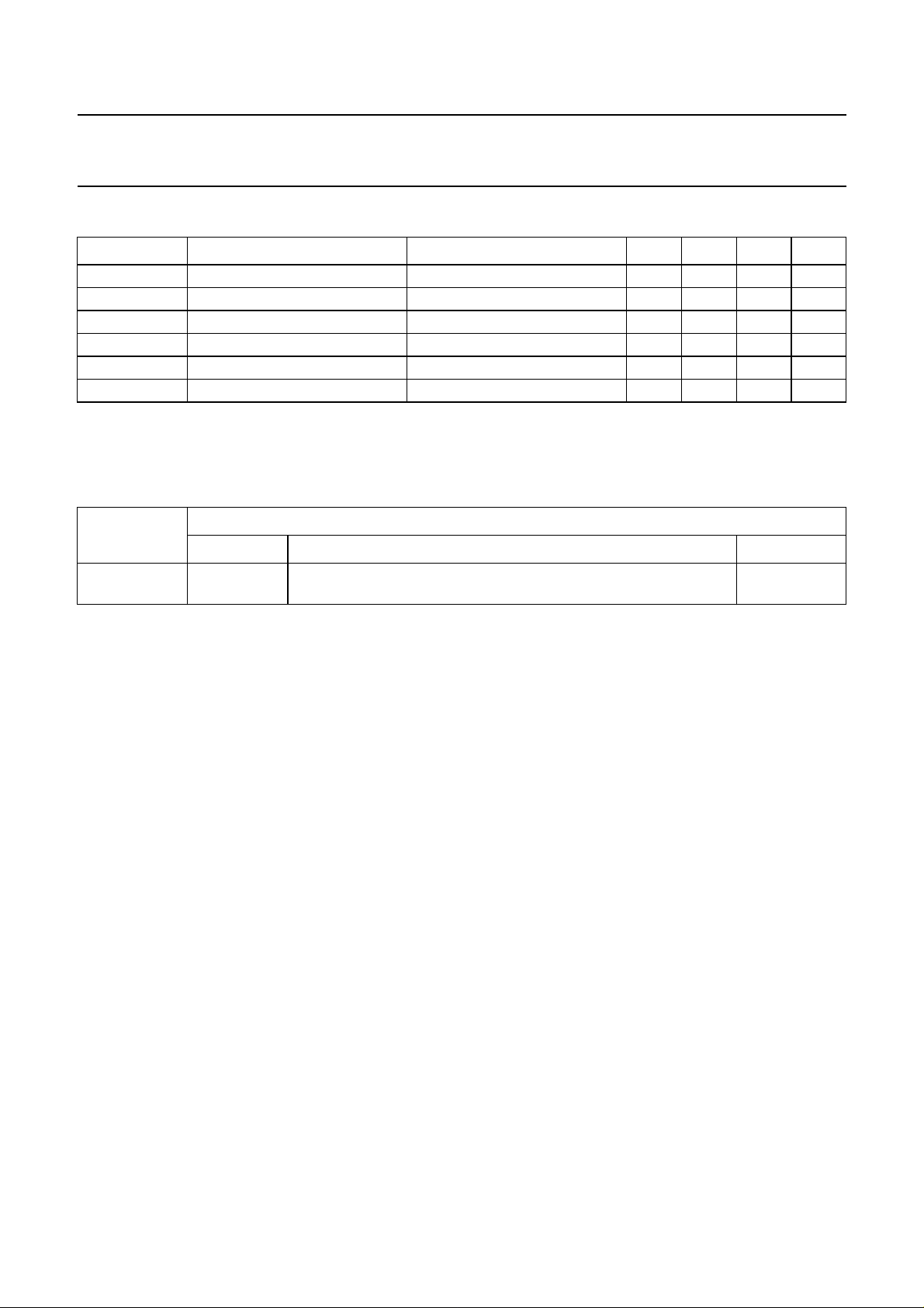
QUICK REFERENCE DATA
SYMBOL PARAMETER CONDITIONS MIN. TYP. MAX. UNIT
V
DD
I
DD
f
sys
f
loop
t
jitter
ς PLL damping factor − 0.7 −−
Note
1. The internal system frequency is 1728 times the H
ORDERING INFORMATION
supply voltage 4.5 5.0 5.5 V
supply current − 200 − mA
system frequency note 1 − 27 − MHz
PLL loop bandwidth frequency 4 −−kHz
PLL short term stability time jitter during 1 line (64 µs) −−4ns
input frequency for both the acquisition and display PLLs.
Sync
TYPE
NUMBER
NAME DESCRIPTION VERSION
PACKAGE
SAB9077H QFP100 plastic quad flat package; 100 leads (lead length 1.95 mm);
body 14 × 20 × 2.8 mm
SOT317-2
1996 Aug 07 3
Page 4
Philips Semiconductors Preliminary specification
Picture-In-Picture (PIP) controller SAB9077H
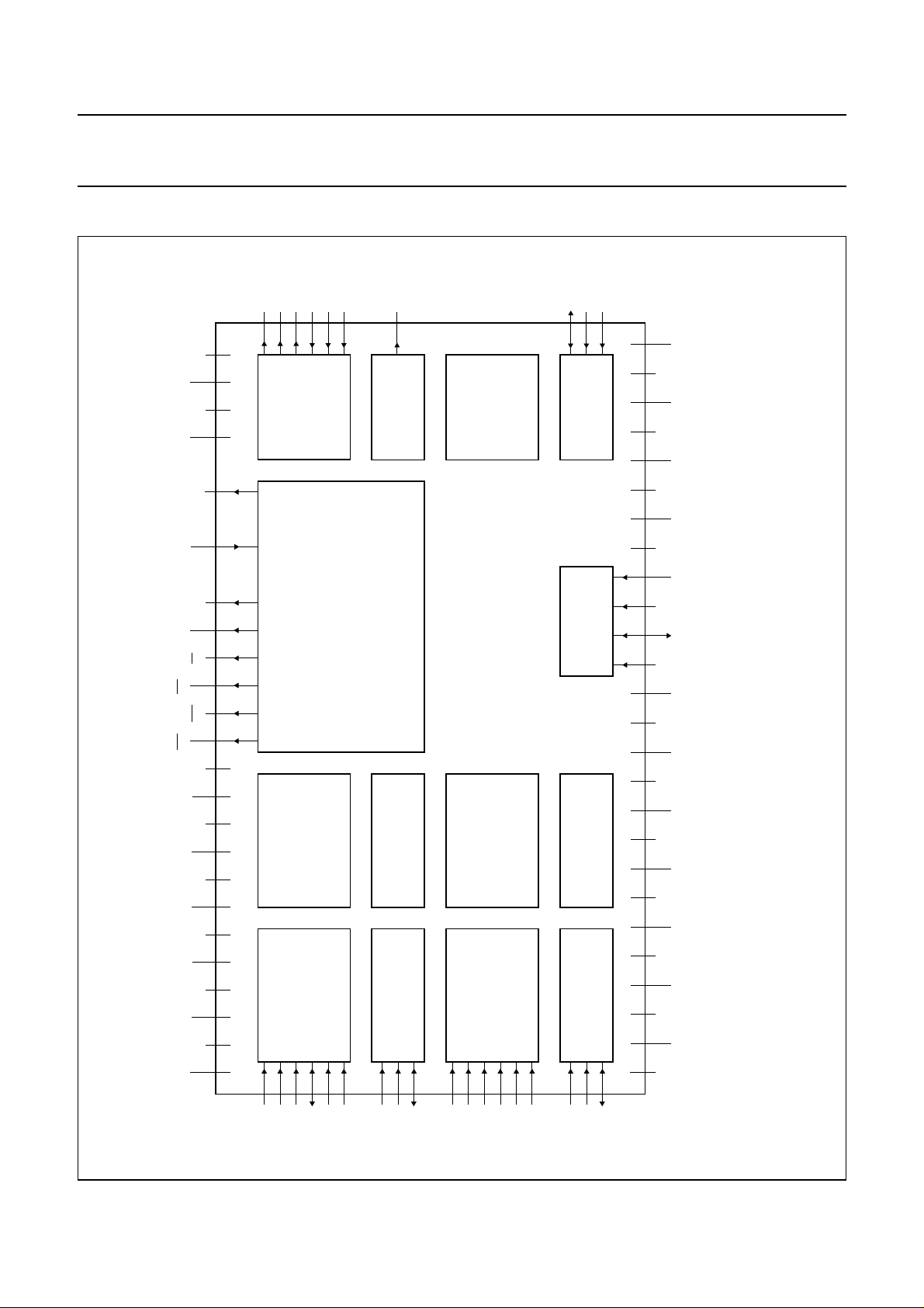
BLOCK DIAGRAM
sync
bias
DPV
DV
sync
DPH
MBH502
DYDUDV
bias
DAV
refT
DAV
refB
DAV
DFB
dbook, full pagewidth
DDA
DAV
SSA
DAV
92 84 83
DDD
DAV
91
SSD
DAV
51, 53, 55,
AD0 to AD8
23, 25, 27,
DAI0 to DAI7
DAO0 to DAO7
31 40 32, 34, 36,
DT
47
WE SC
CAS
49 48
RAS
DDD
MV
SSD
MV
67 13 14
DDD
SV
68
SSD
SV
DDA
SAV
SSA
SAV
77 69 70
DDD
SAV
78
SSD
SAV
DDA
MAV
SSA
MAV
4 12 11
DDD
MAV
3
SSD
MAV
869088
57, 58, 56,
54, 52, 50
29, 30, 28,
26, 24
38, 39, 37,
35, 33
71
DAC
AND
AND
HORIZONTAL
CLAMP AND ADC
75
73
858789
BUFFER
VDRAM CONTROL AND (RE-) FORMATTING
FILTER
VERTICAL
767472
93
DISPLAY
CONTROL
LINE MEMORY
GENERATOR
PLL AND CLOCK
796480
1068
LINE MEMORYSAB9077H
AND
FILTER
VERTICAL
HORIZONTAL
CLAMP AND ADC
579
969495
GENERATOR
PLL AND CLOCK
C-BUS CONTROL
2
I
LINE MEMORY
GENERATOR
PLL AND CLOCK
2171
6318192221201516596061628281 4142434445466566979899
100
TDCLKTM2
TM0
SSD
MCV
SCL
POR
DDD
DCV
SSD
DV
DDD
V
DDD
SCV
SSA
SPV
DDA
DPV
SSA
MPV
TACLKTC
TM1
DDD
MCV
A0
SDA
SSD
DCV
DDD
DV
SSD
V
SSD
SCV
DDA
SPV
SSA
DPV
DDA
MPV
Fig.1 Block diagram.
SYSUSV
bias
SAV
refT
SAV
refB
SAV
syncSVsync
SPH
bias
SPV
1996 Aug 07 4
MYMUMV
bias
MAV
refT
MAV
refB
MAV
syncMVsync
MPH
bias
MPV
Page 5
Philips Semiconductors Preliminary specification
Picture-In-Picture (PIP) controller SAB9077H
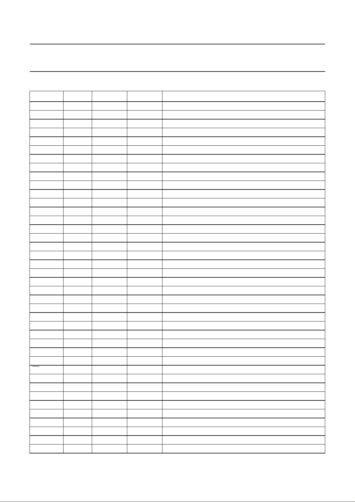
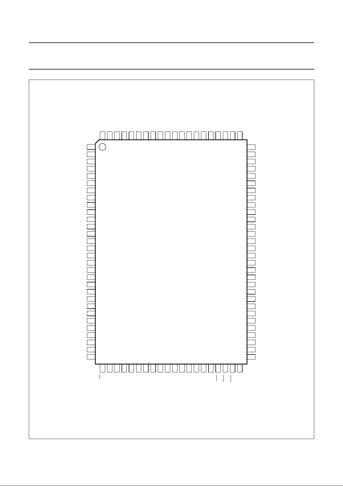
PINNING
SYMBOL PIN I/O TYPE DESCRIPTION
MPV
bias
MPH
sync
MAV
SSD
MAV
DDD
MAV
bias
MU 6 I E027 analog U input for main channel
MAV
refT
MV 8 I E027 analog V input for main channel
MAV
refB
MY 10 I E027 analog Y input for main channel
MAV
DDA
MAV
SSA
MV
SSD
MV
DDD
MCV
DDD
MCV
SSD
MV
sync
TDCLK 18 I HPP01 test clock for display
TC 19 I HPP01 test control
TM0 20 I HPP01 test mode 0
TM1 21 I HPP01 test mode 1
TM2 22 I HPP01 test mode 2
DAI0 23 I HPP04 data bus input from memory; bit 0
DAI7 24 I HPP04 data bus input from memory; bit 7
DAI1 25 I HPP04 data bus input from memory; bit 1
DAI6 26 I HPP04 data bus input from memory; bit 6
DAI2 27 I HPP04 data bus input from memory; bit 2
DAI5 28 I HPP04 data bus input from memory; bit 5
DAI3 29 I HPP04 data bus input from memory; bit 3
DAI4 30 I HPP04 data bus input from memory; bit 4
DT 31 O OPF20 memory data transfer output; active LOW
DAO0 32 O OPF20 data bus output to memory; bit 0
DAO7 33 O OPF20 data bus output to memory; bit 7
DAO1 34 O OPF20 data bus output to memory; bit 1
DAO6 35 O OPF20 data bus output to memory; bit 6
DAO2 36 O OPF20 data bus output to memory; bit 2
DAO5 37 O OPF20 data bus output to memory; bit 5
DAO3 38 O OPF20 data bus output to memory; bit 3
DAO4 39 O OPF20 data bus output to memory; bit 4
SC 40 O OPF20 memory shift clock output
1 I/O E027 analog bias reference for main channel
2 I HPP01 horizontal synchronization for main channel
3 I/O E009 digital ground for main channel ADCs and PLLs
4 I/O E030 digital positive power supply for main channel ADCs and PLLs
5 I E027 analog bias reference for main channel ADCs
7 I E027 analog top reference voltage for main channel ADCs
9 I E027 analog bottom reference voltage for main channel ADCs
11 I/O E030 analog positive power supply for main channel ADCs
12 I/O E009 analog ground for main channel ADCs
13 I/O E009 digital ground for main-channel core
14 I/O E030 digital positive power supply for main-channel core
15 I/O E030 digital positive power supply for main-clock buffer
16 I/O E009 digital ground for main-clock buffer
17 I HPP01 vertical synchronization for main channel
1996 Aug 07 5
Page 6
Philips Semiconductors Preliminary specification
Picture-In-Picture (PIP) controller SAB9077H
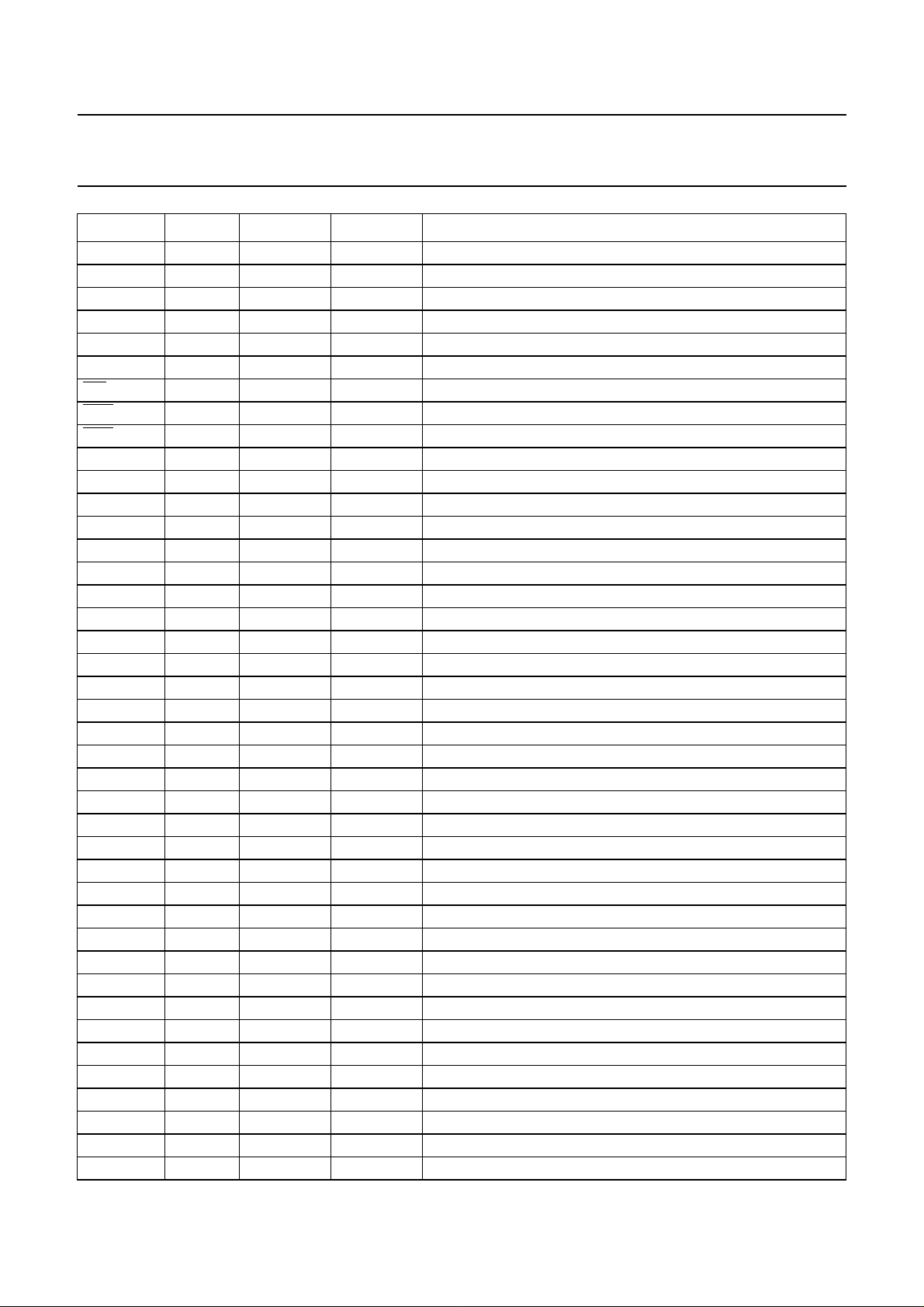
SYMBOL PIN I/O TYPE DESCRIPTION
DCV
SSD
DCV
DDD
DV
DDD
DV
SSD
V
SSD
V
DDD
WE 47 O OPF20 memory write enable output; active LOW
CAS 48 O OPF20 memory column address strobe output; active LOW
RAS 49 O OPF20 memory row address strobe output; active LOW
AD8 50 O OPF20 memory address bus output; bit 8
AD0 51 O OPF20 memory address bus output; bit 0
AD7 52 O OPF20 memory address bus output; bit 7
AD1 53 O OPF20 memory address bus output; bit 1
AD6 54 O OPF20 memory address bus output; bit 6
AD2 55 O OPF20 memory address bus output; bit 2
AD5 56 O OPF20 memory address bus output; bit 5
AD3 57 O OPF20 memory address bus output; bit 3
AD4 58 O OPF20 memory address bus output; bit 4
A0 59 I HPF01 I
SCL 60 I HPP01 shift clock input for I
SDA 61 I/O IOI41 shift I
POR 62 I HUP07 power-on reset input
TACLK 63 I HPP01 test clock for acquisition
SV
sync
SCV
SSD
SCV
DDD
SV
DDD
SV
SSD
SAV
SSA
SAV
DDA
SY 71 I E027 analog Y input for sub-channel
SAV
refB
SV 73 I E027 analog V input for sub-channel
SAV
refT
SU 75 I E027 analog U input for sub-channel
SAV
bias
SAV
DDD
SAV
SSD
SPH
sync
SPV
bias
SPV
SSA
41 I/O E009 digital ground for display-clock buffer
42 I/O E030 digital positive power supply for display-clock buffer
43 I/O E030 digital positive power supply for display core
44 I/O E009 digital ground for display core
45 I/O E009 digital ground for peripherals
46 I/O E030 digital positive power supply for peripherals
2
C-bus address 0 selection input
2
C-bus
2
C-bus input data; acknowledge I2C-bus output data
64 I HPP01 vertical synchronization input for sub-channel
65 I/O E009 digital ground for sub-clock buffer
66 I/O E030 digital positive power supply for sub-clock buffer
67 I/O E030 digital positive power supply for sub-channel core
68 I/O E009 digital ground for sub-channel core
69 I/O E009 analog ground for sub-channel ADCs
70 I/O E030 analog positive power supply for sub-channel ADCs
72 I E027 analog bottom reference voltage for sub-channel ADCs
74 I E027 analog top reference voltage for sub-channel ADCs
76 I/O E027 analog bias reference for sub-channel ADCs
77 I/O E030 digital positive power supply for sub-channel ADCs and PLLs
78 I/O E009 digital ground for sub-channel ADCs and PLLs
79 I HPP01 horizontal synchronization input for sub-channel
80 I/O E027 analog bias reference for sub-channel
81 I/O E009 analog ground for sub-channel PLL
1996 Aug 07 6
Page 7
Philips Semiconductors Preliminary specification
Picture-In-Picture (PIP) controller SAB9077H
SYMBOL PIN I/O TYPE DESCRIPTION
SPV
DDA
DAV
DDA
DAV
SSA
DAV
bias
DY 86 O E027 analog Y output of DAC
DAV
refT
DV 88 O E027 analog V output of DAC
DAV
refB
DU 90 O E027 analog U output of DAC
DAV
SSD
DAV
DDD
DFB 93 O OPF20 fast blanking control output signal
DV
sync
DPH
sync
DPV
bias
DPV
SSA
DPV
DDA
MPV
DDA
MPV
SSA
82 I/O E030 analog positive power supply for sub-channel PLL
83 I/O E030 analog positive power supply for DACs
84 I/O E009 analog ground for DACs
85 I E027 analog bias voltage reference for DACs
87 I E027 analog top reference voltage for DACs
89 I E027 analog bottom reference voltage for DACs
91 I/O E009 digital ground for DACs
92 I/O E030 digital positive power supply for DACs
94 I HPP01 vertical synchronization input for display channel
95 I HPP01 horizontal synchronization input for display PLL
96 I/O E027 analog bias voltage reference for display PLL
97 I/O E009 analog ground for display PLL
98 I/O E030 analog positive power supply for display PLL
99 I/O E030 analog positive power supply for main channel PLL
100 I/O E009 analog ground for main channel PLL
Table 1 Pin type explanation
PIN TYPE DESCRIPTION
E030 V
E009 VSSpin; diode to V
E027 analog input pin; diode to VDD and V
HPF01 digital input pin; CMOS levels, diode to V
HPP01 digital input pin; CMOS levels, diode to VDD and V
pin; diode to V
DD
SS
DD
SS
SS
SS
HUP07 digital input pin; CMOS levels with hysteresis, pull-up resistor to VDD, diode to VDD and V
HOU21 digital IO pin; CMOS levels with hysteresis, pull-up to VDD, diode to VDD and V
IOI41 I2C-bus pull-down output stage; CMOS input levels, diode to V
SS
SS
OPF20 digital output pin; CMOS levels
SS
1996 Aug 07 7
Page 8
Philips Semiconductors Preliminary specification
Picture-In-Picture (PIP) controller SAB9077H
handbook, full pagewidth
MPV
MPH
MAV
MAV
MAV
MAV
MAV
MAV
MAV
MV
MV
MCV
MCV
MV
bias
sync
SSD
DDD
bias
MU
refT
MV
refB
MY
DDA
SSA
SSD
DDD
DDD
SSD
sync
TDCLK
TC
TM0
TM1
TM2
DAI0
DAI7
DAI1
DAI6
DAI2
DAI5
DAI3
DAI4
SSA
DDA
DDA
MPV
MPV
DPV
99989796959493929190898887868584838281
100
1
2
3
4
5
6
7
8
9
10
11
12
13
14
15
16
17
18
19
20
21
22
23
24
25
26
27
28
29
SSA
DPV
bias
DPV
sync
DPH
sync
DV
DDD
DFB
DAV
DAV
SAB9077H
SSD
DU
refB
DAV
DV
refT
DAV
DY
bias
DAV
SSA
DAV
DDA
DAV
DDA
SPV
SSA
SPV
80
79
78
77
76
75
74
73
72
71
70
69
68
67
66
65
64
63
62
61
60
59
58
57
56
55
54
53
52
5130
SPV
bias
SPH
sync
SAV
SSD
SAV
DDD
SAV
bias
SU
SAV
refT
SV
SAV
refB
SY
SAV
DDA
SAV
SSA
SV
SSD
SV
DDD
SCV
DDD
SCV
SSD
SV
sync
TACLK
POR
SDA
SCL
A0
AD4
AD3
AD5
AD2
AD6
AD1
AD7
AD0
31323334353637383940414243444546474849
DT
DAO0
DAO7
DAO1
DAO6
DAO2
DAO5
DAO3
DAO4
Fig.2 Pin configuration.
1996 Aug 07 8
SC
SSD
DCV
DDD
DCV
DDD
DV
SSDVSSD
DV
DDD
V
WE
CAS
RAS
50
AD8
MBH501
Page 9

Philips Semiconductors Preliminary specification
Picture-In-Picture (PIP) controller SAB9077H
FUNCTIONAL DESCRIPTION
Pixel rate
The internal chrominance format used is 4 : 1 : 1. It is
expected that the bandwidth of the input signals is limited
to 4.5 MHz for the Y input and 1.125 MHz for the U/V
inputs.
The Y input is sampled with a 1728 × H
(≈27.0 MHz)
sync
clock and is filtered and down sampled to the internal
864 × H
(≈13.5 MHz) pixel rate.
sync
The U and V inputs are multiplexed and sampled with a
432 × H
216 × H
clock and down sampled to the internal
sync
(≈3.375 MHz) pixel rate.
sync
Acquisition area
Synchronization is done via the acquisition H
V
pins. With the acquisition fine positioning added to a
Sync
Sync
and
system constant the starting point of the acquisition can be
controlled.
The acquisition area is 672 pixels/line and 228 lines/field
for NTSC and 276 lines/field for PAL. Both main and
sub-channel are equivalent in handling the data.
Display mode
The internal display pixel rate is 864 × DPH
sync
which is
13.5 MHz. This pixel rate is upsampled by interpolation to
1728 × DPH
before the DAC stage.
sync
Display area
The display background is an area of 696 pixels for both
PAL and NTSC, 238 lines for NTSC and 286 lines for PAL.
This can be put on/off by the BGON bit independent of the
PIPON bits. This area can be moved by the display
background fine positioning (BGHFP and BGVFP).
Its colour is determined by the BGCOL and BGBRT bits.
Within this area PIPs are defined dependent on the
PIP mode. The PIP sizes are determined by the display
reduction factors as is shown in Table 2. Whether a PAL or
NTSC fixed number is used is depends on the DPAL bit.
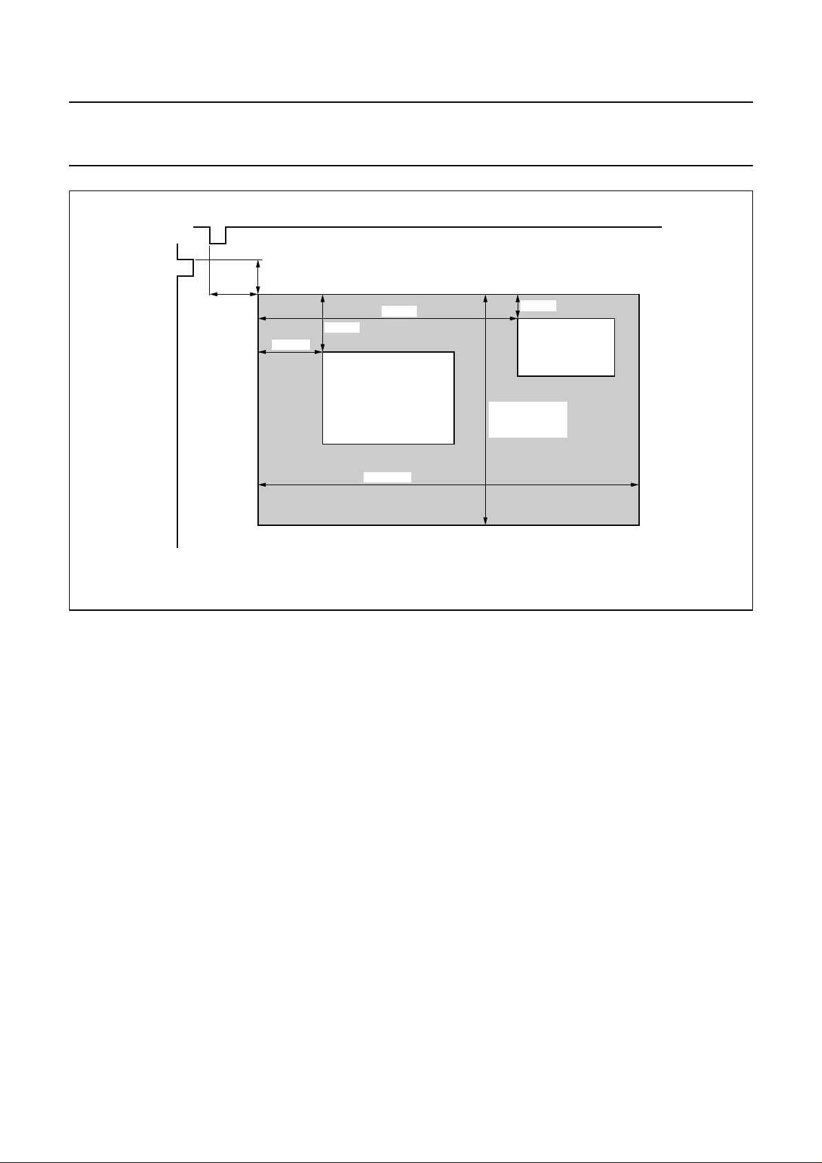
The display fine positioning determines the location of the
PIPs with respect to the background. sub and
main-channel both have their independent PIP size and
location control, which is shown in Fig.3.
Table 2 PIP sizes
REDUCTION H/1 H/2 H/3 H/4 V/1 V/2 V/3 V/4
Pixels 672 336 224 168 −−−−
NTSC-lines −−−−228 114 76 57
PAL-lines −−−−276 138 92 69
1996 Aug 07 9
Page 10
Philips Semiconductors Preliminary specification
Picture-In-Picture (PIP) controller SAB9077H
handbook, full pagewidth
BGHFP
BGVFP
SAHFP
MAVFP
MAHFP
MAIN CHANNEL
696 pixels
Fig.3 Display fine positioning.
PIP modes
The two independent acquisition channels can also be
controlled independently on the display side. A wide
variety of modes is possible but a subset of 7 modes is
fixed and can be set easily by the I2C-bus. An overview of
the preconditioned modes is given in Table 3. For all PIP
modes the main and sub-display fine positioning must be
set to obtain a display configuration.
D
ATA TRANSFER
The internal data path has an 8-bit resolution and 4 :1:1
data format. The communication to the external VDRAM
takes place at 864 × H
(both display and acquisition).
sync
SAVFP
SUB CHANNEL
238 lines (NTCS)
or
286 lines (PAL)
MBH503
Approximately 800 8-bit words can be fetched from the
external VDRAM in one display line which is not enough to
display one complete display line with true 8-bit resolution.
Two methods of reducing data are available. One is simply
skipping the 8-bit to 6-bit (SKIP6, I2C-bus bit) and the other
is a small form of data reduction to come from 8-bit to 6-bit
(SMART6, I2C-bus bit). If both bits are set to logic 0 the
device is in true 8-bit resolution mode. For the twin PIP
mode the main channel is not placed in the VDRAM but in
an internal buffer, 8 bit resolution is then possible for both
PIPs.
1996 Aug 07 10
Page 11

Philips Semiconductors Preliminary specification
Picture-In-Picture (PIP) controller SAB9077H
Table 3 PIP modes
PIP MODES SUB-CHANNEL MAIN CHANNEL SUB-CHANNEL MAIN CHANNEL
NAME FIGURE MODE REDH REDV REDH REDV HFP VFP HFP VFP
SP SP small 0000
SP SP medium 0000
SP SP large 0000
1
⁄
4
1
⁄
3
1
⁄
2
SP SP small 0000 −−
SP SP medium 0000 −−
SP SP large 0000 −−
DP DP 0000
DP twin PIP 1001
MP3L POP-left 0010
1
⁄
2
1
⁄
2
1
⁄
4
MR3R POP-right 0010 −−
MR3D POP-double 0010
MP7 POP-double 0011
MP8 MP7 0011
MP4 Quatro 0001
MP9 MP9 0100
MP16 MP16 0101
MP16 MP16 mix 0110
FFS full field still 0000
1
⁄
4
1
⁄
4
1
⁄
4
1
⁄
2
1
⁄
3
1
⁄
4
1
⁄
4
1
⁄
1
FFL full field live 1000 −−
MAN manual X111 X X X X X X X X
1
⁄
4
1
⁄
3
1
⁄
2
1
⁄
2
1
⁄
1
1
⁄
4
1
⁄
4
1
⁄
4
1
⁄
4
1
⁄
2
1
⁄
3
1
⁄
4
1
⁄
4
1
⁄
1
−−−−−−
−−−−−−
−−−−−−
1
⁄
4
1
⁄
3
1
⁄
2
1
⁄
2
1
⁄
2
1
⁄
4
1
⁄
3
1
⁄
2
1
⁄
2
1
⁄
1
−−−−
−−−−
−−−−
03H 46H 57H 46H
03H 05H 57H 05H
−−08H 10H −−
1
⁄
4
1
⁄
4
1
⁄
4
1
⁄
4
−−72H 10H
08H 10H 72H 10H
−−03H 05H −−
1
⁄
2
1
⁄
2
1
⁄
3
1
⁄
2
1
⁄
2
1
⁄
3
03H 05H 44H 20H
03H 05H 03H 77H
03H 05H 51H 3BH
−−03H 05H −−
1
⁄
4
1
⁄
4
03H 05H 03H 77H
−−03H 05H −−
1
⁄
1
1
⁄
1
−−03H 05H
COMBINATIONS
PIP
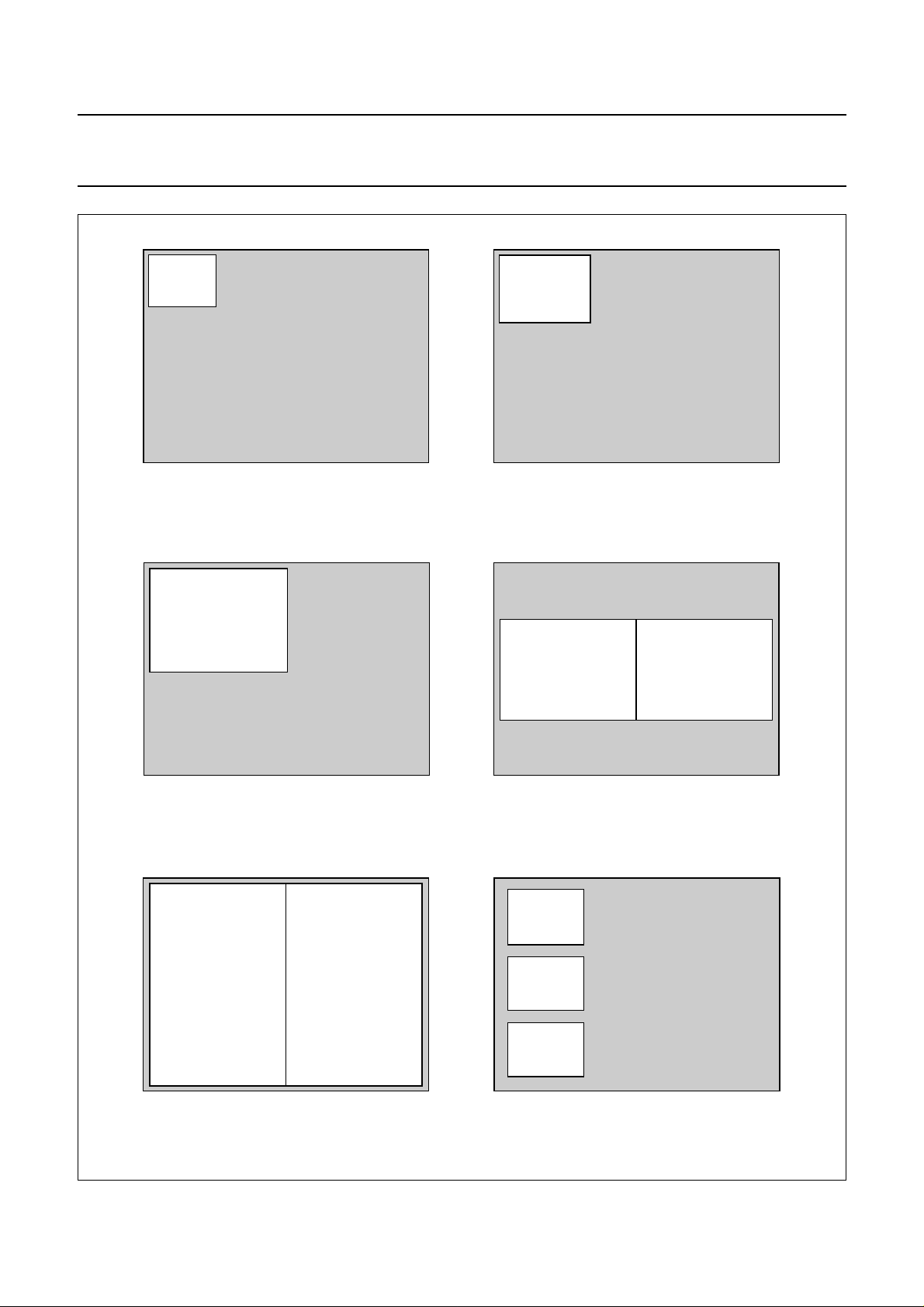
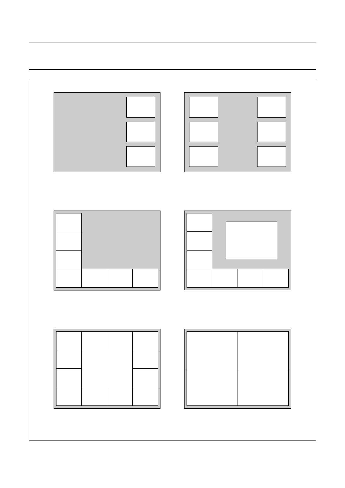
Figures 4, 5 and 6 provide an overview of possible combinations as they can be shown on the screen.
An example of fine positioning is given in the right four columns of Table 3.
More PIP modes can be obtained by varying the horizontal and vertical reduction factors to meet correct aspect ratios
when using 16 : 9 screens.
In manual mode more PIP modes become available. Table 6 with associating text describes how to setup a PIP mode.
1996 Aug 07 11
Page 12
Philips Semiconductors Preliminary specification
Picture-In-Picture (PIP) controller SAB9077H
handbook, halfpage
handbook, halfpage
SP-Small
MGD594
handbook, halfpage
handbook, halfpage
SP-Medium
MGD595
SP-Large
handbook, halfpage
Twin-PIP
MGD596
MGD598
Fig.4 PIP Modes.
1996 Aug 07 12
handbook, halfpage
DP
POP-Left
MGD597
MGD588
Page 13
Philips Semiconductors Preliminary specification
Picture-In-Picture (PIP) controller SAB9077H
handbook, halfpage
handbook, halfpage
POP-Right
MGD589
handbook, halfpage
handbook, halfpage
POP-Double
MGD590
MP7
handbook, halfpage
MP13
MGD591
MGD593
Fig.5 PIP Modes.
1996 Aug 07 13
handbook, halfpage
MP8
Quatro
MGD592
MGD584
Page 14

Philips Semiconductors Preliminary specification
Picture-In-Picture (PIP) controller SAB9077H
handbook, halfpage
handbook, halfpage
MP9
MGD585
handbook, halfpage
MP16
MGD586
Full Field Still
MGD587
Full Field Live
Fig.6 PIP Modes.
1996 Aug 07 14
Page 15

Philips Semiconductors Preliminary specification
Picture-In-Picture (PIP) controller SAB9077H
2
I
I2C-bus description
The I2C-bus provides bidirectional 2-line communication
between different ICs. The SDA line is the serial data line
and SCL serves as serial clock line. Both lines must be
connected to a positive supply via a pull-up resistor when
connected to the output stages of a device. Data transfer
may be initiated only when the bus is not busy.
The SAB9077H has the I2C-bus addresses 2C and 2E,
switchable by the pin A0. Valid subaddresses are
00H to 18H (Table 4) and 20H to 32H (Table 6).
2
Table 4 Overview of I
C-bus addresses
C-bus control is in accordance with the I2C-bus protocol.
First a START sequence must be put on the I2C-bus, then
the I2C-bus address of the circuit must be send, followed
by a subaddress. After this sequence the data of the
subaddresses must be sent. An auto-increment function
gives the option to send data of the incremented
subaddresses until a STOP sequence is send.
Table 4 gives an overview of the I2C-bus addresses.
SA
DATA BYTE
BIT 7 BIT 6 BIT 5 BIT 4 BIT 3 BIT 2 BIT 1 BIT 0
00H MPIPON SPIPON MFREEZE SFREEZE MCOPY PIPMODE2 PIPMODE1 PIPMODE0
01H note 1 note 1 M1FLD S1FLD NIPCOFF DNONINT MNONINT SNONINT
02H DFILT FILLOFF SMART6 SKIP6 YTH3 YTH2 YTH1 YTH0
03H BGHFP3 BGHFP2 BGHFP1 BGHFP0 BGVFP3 BGVFP2 BGVFP1 BGVFP0
04H SDHFP7 SDHFP6 SDHFP5 SDHFP4 SDHFP3 SDHFP2 SDHFP1 SDHFP0
05H SDVFP7 SDVFP6 SDVFP5 SDVFP4 SDVFP3 SDVFP2 SDVFP1 SDVFP0
06H MDHFP7 MDHFP6 MDHFP5 MDHFP4 MDHFP3 MDHFP2 MDHFP1 MDHFP0
07H MDVFP7 MDVFP6 MDVFP5 MDVFP4 MDVFP3 MDVFP2 MDVFP1 MDVFP0
08H MDREDH1 MDREDH0 MDREDV1 MDREDV0 SDREDH1 SDREDH0 SDREDV1 SDREDV0
09H MAREDH1 MAREDH0 MAREDV1 MAREDV0 SAREDH1 SAREDH0 SAREDV1 SAREDV0
0AH MAHFP3 MAHFP2 MAHFP1 MAHFP0 SAHFP3 SAHFP2 SAHFP1 SAHFP0
0BH SAVFP7 SAVFP6 SAVFP5 SAVFP4 SAVFP3 SAVFP2 SAVFP1 SAVFP0
0CH MAVFP7 MAVFP6 MAVFP5 MAVFP4 MAVFP3 MAVFP2 MAVFP1 MAVFP0
0DH MLSEL3 MLSEL2 MLSEL1 MLSEL0 SLSEL3 SLSEL2 SLSEL1 SLSEL0
0EH MBSEL3 MBSEL2 MBSEL1 MBSEL0 SBSEL3 SBSEL2 SBSEL1 SBSEL0
0FH BHSIZE3 BHSIZE2 BHSIZE1 BHSIZE0 BVSIZE3 BVSIZE2 BVSIZE1 BVSIZE0
10H note 1 SBON SBBRT1 SBBRT0 note 1 SBCOL2 SBCOL1 SBCOL0
11H note 1 SBSON SBSBRT1 SBSBRT0 note 1 SBSCOL2 SBSCOL1 SBSCOL0
12H note 1 MBON MBBRT1 MBBRT0 note 1 MBCOL2 MBCOL1 MBCOL0
13H note 1 MBSON MBSBRT1 MBSBRT0 note 1 MBSCOL2 MBSCOL1 MBSCOL0
14H note 1 BGON BGBRT1 BGBRT0 note 1 SBGCOL2 SBGCOL1 SBGCOL0
15H note 1 note 1 note 1 SVFILT SUVPOL SVSPOL SHSYNC SFPOL
16H note 1 note 1 note 1 MVFILT MUVPOL MVSPOL MHSYNC MFPOL
17H note 1 FBDEL2 FBDEL1 FBDEL0 DUVPOL DVSPOL DHSYNC DFPOL
18H PEDESTV3 PEDESTV2 PEDESTV1 PEDESTV0 PEDESTU3 PEDESTU2 PEDESTU1 PEDESTU0
Note
1. The data bits which are not used should be set to zero.
1996 Aug 07 15
Page 16

Philips Semiconductors Preliminary specification
Picture-In-Picture (PIP) controller SAB9077H
SA 00H PIP REGISTER
MPIPON and SPIPON bits switch respectively the main
and sub PIPs of the SAB9077H on or off. The MFREEZE
and SFREEZE bits make the current live pictures for the
Main and Sub frozen. The writing to the VDRAM is
stopped.
The MCOPY bit copies the Main data direct to the output.
This mode should only be set when MREDV is 1/1. Table 2
gives more information when to set this bit. The PIPMODE
bits set the PIP mode in accordance with Table 3.
SA 01H
M1FLD and S1FLD
DISPLAY REGISTER
(1)
bits control the use of the reserved
second field in the VDRAM. If this bit is set to logic 0 then
address spaces are reserved for both fields in the VDRAM.
This avoids joint line errors. Whether these address
spaces are used is dependent on the interlacing of the
input signals and the NONINT bits. If a 1FLD bit is set to
logic 1 then only 1 address space is used in the VDRAM
for both fields. In some PIP modes the use of a second
field is not possible since there is not enough space in the
VDRAM, in these modes the 1FLD bit must be set to
logic 1. The DNONINT bit controls the interlace mode of
the display part. If set to logic 1 then data is only read from
one field in the VDRAM. If set to logic 0 then both fields (if
available) are used for display.
MNONINT and SNONINT bits control the interlace mode
of the acquisition blocks. If set to logic 1 then data is only
written to one field in the VDRAM (two fields remain
allocated). If set to logic 0 then both fields (if available) are
used for acquisition.
The NIPCOFF bit determines whether a grey bar is
inserted in case a NTSC PIP is displayed in a PIP with PAL
PIP size. The missing lines are equally divided between
the top part and the bottom part of the PIP window and
made 30% grey. If this bit is set to logic 0 the grey bar is
displayed, if this bit is set to logic 1 the grey bar is omitted
and the PIP data is shifted up.
SA 02H
DISPLAY REGISTER
The DFILT bit controls an interpolating filter that changes
the internal 864 pixels data rate to the output data rate of
2 × 864 pixels. If DFILT is set to logic 1 then the filter is on.
The FILLOFF bit controls filling of PIPs when the PIP mode
is switched. If FILLOFF is set to logic 0 then all PIPs are
filled with a 30% gray until their channel has been updated.
If FILLOFF is set to logic 1 then the VDRAM content is
always visible. This is useful when a new, ‘similar’ to the
previous one, PIP mode is set. The previous data can then
be displayed.
The SMART6 and SKIP6 bits control the data transfer
mode to the external VDRAM. For modes which display a
complete line (672 pixels) a form of data reduction has to
be carried out.
Two transfer modes are available. One is simply skipping
the 8-bit data path to 6-bit (SKIP6). The other is carry out
an intelligent data reduction which keeps an 8-bit
resolution (SMART6).
The YTH bits control the video output. If the current
Y-value is less then YTH × 16 then the fast blank is
switched off, the original live background will be visible.
This feature can be used to pick up sub-titles and display
them as On-Screen Display (OSD) anywhere on the
screen.
SA 03H
DISPLAY BACKGROUND FINE POSITIONING REGISTER
The BGHFP bits control the horizontal display positioning
of the background. The resolution is 16 steps of 4 pixels.
The BGVFP bits control the vertical display positioning of
the background. The resolution is 16 steps of 2 lines/field.
The background fine positioning moves the complete
display. It is a general offset of all the PIP pictures and
background, It is only meant to adjust once the centring of
all PIP modes (see Fig.3).
SA 04H
POSITIONING REGISTERS
AND SA 05H DISPLAY SUB-CHANNEL FINE
These registers control the horizontal and vertical fine
positioning of the display sub-channel with respect to the
display background. This is the actual fine positioning (see
Fig.3). The horizontal resolution is 256 steps of 4 pixels
and the vertical resolution is 256 steps of 1 line/field.
SA 06H
POSITIONING REGISTERS
AND SA 07H DISPLAY MAIN-CHANNEL FINE
These registers control the horizontal and vertical fine
positioning of the display main-channel with respect to the
display background. This is the actual fine positioning (see
Fig.3). The horizontal resolution is 256 steps of 4 pixels
and the vertical resolution is 256 steps of 1 line/field.
(1) If the 1 FLD bits are set to logic 1 the NONINT bits of the
corresponding channel must also be set to logic 1.
1996 Aug 07 16
Page 17

Philips Semiconductors Preliminary specification
Picture-In-Picture (PIP) controller SAB9077H
SA 08H DISPLAY REDUCTION FACTORS REGISTER
This register sets the display reduction factors,
independent of the acquisition reduction factors.
It sets the PIP size to a certain default value in such a way
that the border drawn around the PIP is just fitting.
SA 09H
ACQUISITION REDUCTION FACTORS REGISTER
This register sets the acquisition reduction factors,
independent of the display reduction factors. If the HRED
is 1 to 1 then the VRED must also be 1 : 1.
Restrictions are:
• The DREDH and AREDH must be the same
• The DREDV is equal or smaller than the AREDV
(e.g DREDV is 1 to 2 and AREDV is 1 : 1).
SA 0AH
REGISTERS
AND SA 0CH ACQUISITION FINE POSITIONING
These registers determine the start of the acquisition area.
Horizontal fine positioning can be adjusted with 16 steps of
2 pixels, vertical fine positioning can be adjusted with
256 steps of 1 line/field.
SA 0DH
AND SA 0EH SELECTION REGISTERS
The MLSEL and SLSEL bits control which PIP is live.
Both main channel and sub-channel can have one live
PIP. Counting is done from upper-left to lower-right.
The MBSEL and SBSEL bits control which PIP border has
a different colour. Both main and sub-channel can have a
different PIP channel border selection. Counting is done
from upper-left to lower-right.
SA 10H
COLOUR OF SUB
AND SA 11H BORDER COLOUR AND BORDER SELECT
-CHANNEL REGISTERS (see Table 5)
If SBON is set to logic 1 then the border of the sub-channel
is visible.The SBBRT and SBCOL bits control the
brightness and colour of the sub-channel border colour.
If SBSON is set to logic 1 then one sub-PIP border can
have a different colour. This border is selected by the
SBSEL bits.
The SBSBRT and SBSCOL bits control the brightness and
colour of the sub-border selection colour.
SA 12H
SELECTION COLOUR OF MAIN CHANNEL REGISTERS
AND SA 13H BORDER COLOUR AND BORDER
(see Table 5)
If MBON is set to logic 1 then the border of the main
channel is visible.
The MBBRT and MBCOL bits control the brightness and
colour of the main-channel border colour. If MBSON is set
to logic 1 then one main PIP border can have a different
colour. This PIP is selected by the MBSEL bits, the
function can be switched on if MBSON is set to logic 1.
The MBSBRT and MBSCOL bits control the brightness
and colour of the main-border selection colour.
SA 14H
BACKGROUND CONTROL REGISTER (see Table 5)
If BGON is set to logic 1 then the background is visible.
The BGBRT and BGCOL bits control the brightness and
colour of the background colour.
SA 0FH
BORDER SIZE REGISTER
This register controls the border size. The minimum
horizontal border is 2 pixels. The minimum vertical border
is 1 line. The vertical border size is multiplied by the
FH mode number before it is displayed on the screen.
1996 Aug 07 17
Page 18
Philips Semiconductors Preliminary specification
Picture-In-Picture (PIP) controller SAB9077H
Table 5 Colour types and brightness levels
COLOUR TYPE BRIGHTNESS LEVEL
COLOUR VALUE 4H 5H 6H 7H
Black 0H 0% 10% 30% 50%
Blue 1H 30% 50% 70% 100%
Red 2H 30% 50% 70% 100%
Magenta 3H 30% 50% 70% 100%
Green 4H 30% 50% 70% 100%
Cyan 5H 30% 50% 70% 100%
Yellow 6H 30% 50% 70% 100%
White 7H 60% 70% 80% 100%
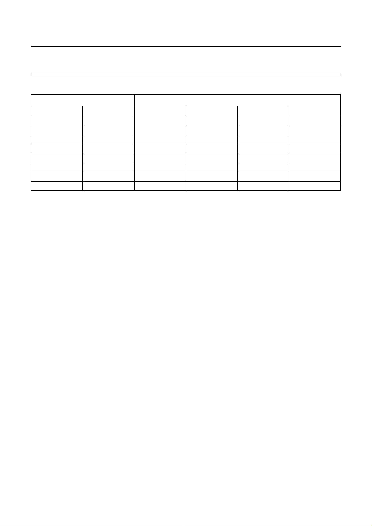
Table 5 indicates how I2C-bus register settings control the
colour and brightness. All colour registers are similar, they
contain one on/off bit, two brightness bits and three colour
type bits. To determine which colour is visible in the event
two or more colours being displayed on the same position,
the next priority scheme is followed:
1. Sub-select colour (SBS)
2. Sub-border colour (SB)
3. Main-select colour (MBS)
4. Main-border colour (MB)
5. Background colour (BG).
SA 15H
AND SA 16H DECODER REGISTERS
The MVFILT and SVFILT bits can set the type of vertical
filtering. The MUVPOL and SUVPOL bits invert the UV
polarity of the incoming signals. The MVSPOL and
SVSPOL bits determine the active edge of the V
sync
(see
Fig.7). The MHSYNC and SHSYNC bits determine the
timing of the H
pulse (burstkey or H
sync
sync
timing).
The MFPOL and SFPOL bits can invert the field
identification (ID) of the incoming fields (see Fig.7).
SA 17H DISPLAY SETTINGS REGISTER
The FBDEL bits can adjust the fast blank delay in 8 steps
of1⁄2 a clock cycle (−8 to +7). 0H is mid-scale.
The DUVPOL bit inverts the UV polarity of the border
colours.
The DVSPOL bit determines the active edge of the V
sync
(see Fig.7). The DHSYNC bit determines the timing of the
H
pulse (burstkey or H
sync
). The DFPOL bit can invert
sync
the field ID of the incoming fields (see Fig.7).
SA 18H
PEDESTAL SETTINGS REGISTER
The PEDESTU and PEDESTV bits give the U and V DAC
outputs an offset of −8 to +7 LSB when the FBL is
switched off. This can be used to adjust the White point of
the system.
1996 Aug 07 18
Page 19

Philips Semiconductors Preliminary specification
Picture-In-Picture (PIP) controller SAB9077H
Additional I2C-bus settings
2
Table 6 Overview of additional I
C-bus sub-addresses
SA
BIT 7 BIT 6 BIT 5 BIT 4 BIT 3 BIT 2 BIT 1 BIT 0
20H PRIO DPAL MPAL SPAL MVRPN1 MVRPN0 SVRPN1 SVRPN0
21H MHRPO31 MHRPO30 MHRPO21 MHRPO20 MHRPO11 MHRPO10 MHRPO1 MHRPO0
22H MHRPN31 MHRPN30 MHRPN21 MHRPN20 MHRPN11 MHRPN10 MHRPN1 MHRPN0
23H MHPIC7 MHPIC6 MHPIC5 MHPIC4 MHPIC3 MHPIC2 MHPIC1 MHPIC0
24H MVPIC7 MVPIC6 MVPIC5 MVPIC4 MVPIC3 MVPIC2 MVPIC1 MVPIC0
25H MHDIS07 MHDIS06 MHDIS05 MHDIS04 MHDIS03 MHDIS02 MHDIS01 MHDIS00
26H MHDIS17 MHDIS16 MHDIS15 MHDIS14 MHDIS13 MHDIS12 MHDIS11 MHDIS10
27H MHDIS27 MHDIS26 MHDIS25 MHDIS24 MHDIS23 MHDIS22 MHDIS21 MHDIS20
28H MHDIS37 MHDIS36 MHDIS35 MHDIS34 MHDIS33 MHDIS32 MHDIS31 MHDIS30
29H MVDIS7 MVDIS6 MVDIS5 MVDIS4 MVDIS3 MVDIS2 MVDIS1 MVDIS0
2AH SHRPO31 SHRPO30 SHRPO21 SHRPO20 SHRPO11 SHRPO10 SHRPO01 SHRPO00
2BH SHRPN31 SHRPN30 SHRPN21 SHRPN20 SHRPN11 SHRPN10 SHRPN01 SHRPN00
2CH SHPIC7 SHPIC6 SHPIC5 SHPIC4 SHPIC3 SHPIC2 SHPIC1 SHPIC0
2DH SVPIC7 SVPIC6 SVPIC5 SVPIC4 SVPIC3 SVPIC2 SVPIC1 SVPIC0
2EH SHDIS07 SHDIS06 SHDIS05 SHDIS04 SHDIS03 SHDIS02 SHDIS01 SHDIS00
2FH SHDIS17 SHDIS16 SHDIS15 SHDIS14 SHDIS13 SHDIS12 SHDIS11 SHDIS10
30H SHDIS27 SHDIS26 SHDIS25 SHDIS24 SHDIS23 SHDIS22 SHDIS21 SHDIS20
31H SHDIS37 SHDIS36 SHDIS35 SHDIS34 SHDIS33 SHDIS32 SHDIS31 SHDIS30
32H SVDIS7 SVDIS6 SVDIS5 SVDIS4 SVDIS3 SVDIS2 SVDIS1 SVDIS0
DATA BYTE
Additional I2C-bus register and PIP modes become
available in sub addresses 20H to 32H.
An overview of these I2C-bus registers is given in Table 6.
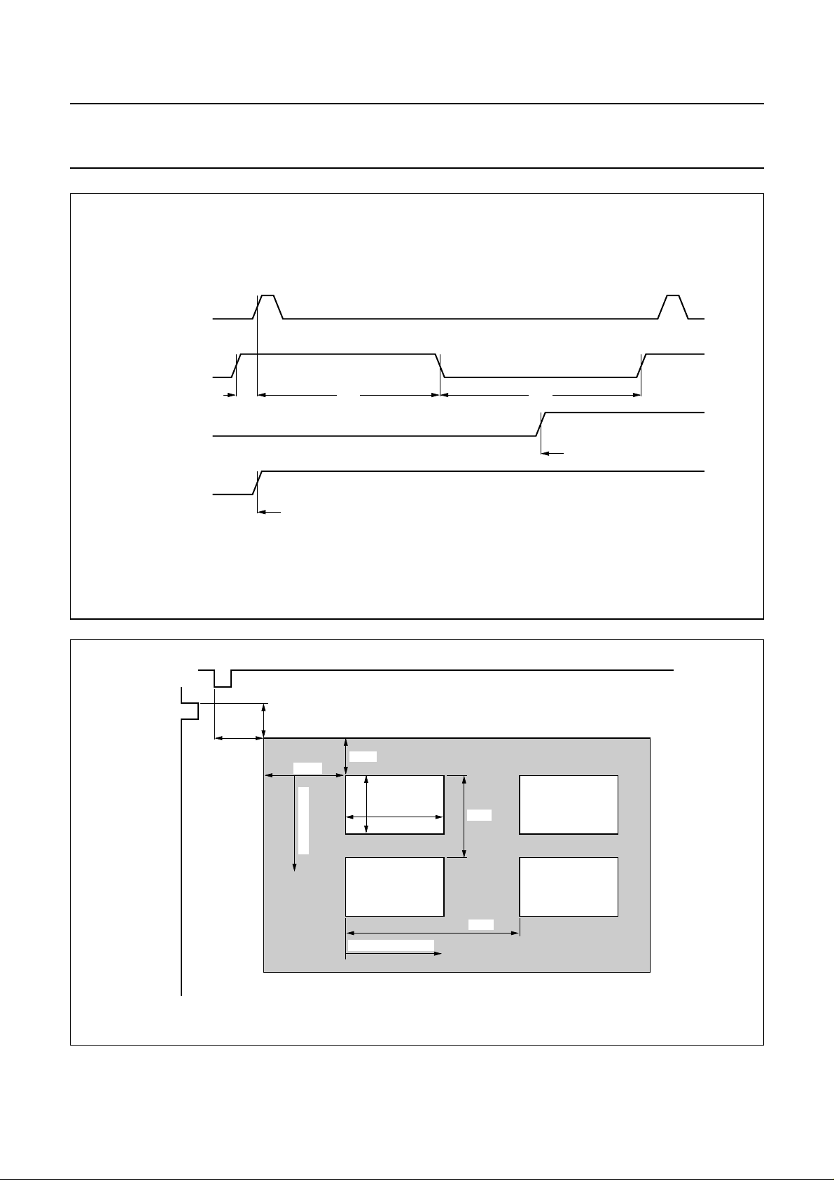
The meaning and relation of theI2C-bus registers is shown
in Fig.8. The background has a fixed size and can be fine
positioned with BGHFP and BGVFP bits. The shown PIPs
are only for one channel (main or sub), the other channel
has the same control and can be displayed at the same
time. The SDHFP and MDHFP bits determine the most left
shown pixel for this channel in 256 steps of 4 pixels.
The SDVFP and MDVFP bits determine the most upper
shown pixel for this channel in 256 steps of 1 line.
The SHPIC and MHPIC bits determine the horizontal
picture size in 256 steps of 4 pixels, the minimum value is
4 pixels. The SVPIC and MVPIC bits determine the vertical
picture size in 256 steps of 1 line, the minimum value is
1 line. The PIP mode is built-up of a maximum of four
horizontal rows. The minimum is one row, more rows can
be displayed by setting the vertical repetition rate number
1996 Aug 07 19
VRPN bits.
The distance between the rows can be set by the SVDIS
and MVDIS bits. Every row is built-up of a maximum of four
PIPs. The minimum is one PIP, additional PIPs can be
added with the HRPN values. The SHRPO and MHRPO
bits determine the offset distance between the starting
points of the first PIP. The distances between the starting
points of the PIPs on a row are determined by the SHDIS
and MHDIS bits.
SA 20H
The PRIO bit sets the priority between main and sub
channel. If PRIO is set to logic 0 priority is given to the sub
channel which means that the sub channel PIPs, if
present, are placed on top of the main PIPs. If PRIO is set
to logic 1 it places the main PIPs on top of the sub PIPs.
The DPAL bit sets the correct default values for PAL on the
display side. The background is enlarged from
238 lines/field to 288 lines/field.
CONTROL REGISTER
Page 20

Philips Semiconductors Preliminary specification
Picture-In-Picture (PIP) controller SAB9077H
The MPAL and SPAL bits set the acquisition area. When
set to logic 1 the acquisition area is enlarged from
228 lines/field (NTSC) to 276 lines/field (PAL).
The MVRPN and SVRPN bits determine the number of
repeated PIP rows. There is always one row visible of each
channel. If no PIPs should be visible the PIP channel must
be switched off (SA 00, bit 7 or bit 6).
SA 21H
REGISTERS FOR ROW
AND SA 2AH: HORIZONTAL REPETITION OFFSET
0 TO 3
The horizontal repetition offsets (MHRPO and SHRPO)
are strongly related to the horizontal distance (MHDIS and
SHDIS bits). These bits set for each row a certain grid of
possible starting points for the PIPs in that row. Every grid
point has a number 0 (the most left PIP), 1, 2 or 3.
The SHRPO and MHRPO bits determine the first grid
number which will be displayed. This mechanism can be
set for each row.
SA 22H
REGISTERS FOR ROW
AND SA 2BH: HORIZONTAL REPETITION NUMBER
0 TO 3
The horizontal repetition numbers (MHRPO and SHRPO)
determine how many times the PIPs are repeated in a row,
once the first PIP is displayed. The repeated PIPs stay in
the grid determined by the SHDIS and MHDIS bits for that
row. This mechanism can be set for each row
independently.
SA 23H
REGISTERS
AND SA 24H; SA 2CH AND SA 2DH: PICTURE SIZE
The MHPIC and SHPIC bits determine the horizontal PIP
size in 256 steps of 4 pixels. The MVPIC and SVPIC bits
determine the vertical PIP size line in 256 steps of 1 line
for NTSC or 256 steps of 2 lines for PAL.
SA 25H
TO SA 29H; SA 2EH TO SA 32H: PICTURE
DISTANCE REGISTERS
For each row the distance between starting points of PIPs
can be set with the MHDIS and SHDIS bits in 256 steps of
4 pixels. The distance between two rows can be set with
the MVDIS and SVDIS bits in 256 steps of 1 line.
Acquisition channel ADCs
Both channels convert the analog input signals to digital
signals by means of two ADCs for each channel.
The internal input levels of the ADCs of each channel are
equal and can be set by the AV
refT
and AV
refB
pins.
The reference levels are made internally by means of a
resistor network which divides the analog voltage to a
default set of preferred levels. External capacitors are
needed to filter AC components on the reference levels.
The resolution of the ADCs is 8-bit; Differential
Non-Linearity (DNL) is 7-bit; Integral Non-Linearity (INL) is
6-bit, and the sampling is done at the system frequency of
27 MHz for the Y-input. The U/V inputs are multiplexed
and sampled at 13.5 MHz. The analog input signals are
amplified to make maximum use of the dynamic range of
the ADCs. A bias voltage V
is used for decoupling AC
bias
components on internal references. The inputs should be
AC-coupled and an internal clamp circuit will clamp the
input to AV
AV
refT
-----------------------------------------
for the luminance channels and to
refB
AV
–
refB
2
for the chrominance channels.
The clamping starts at the leading edge of the burst key
pulse.
Output DACs
The digitally processed signals are converted to analog
signals by means of three 8-bit DACs. The output voltages
of these DACs are default set by the DAV
level and DAV
pin for the bottom level. Default values
refB
pin for the top
refT
are 1.5 V.
External memory
For the external memory two VDRAMs of type Mitsubishi
M5M442256 are foreseen. They have a storage capacity
of 262144 words of 4-bit each and will be used in parallel.
It is also possible to use one 2 Mbit VDRAM of
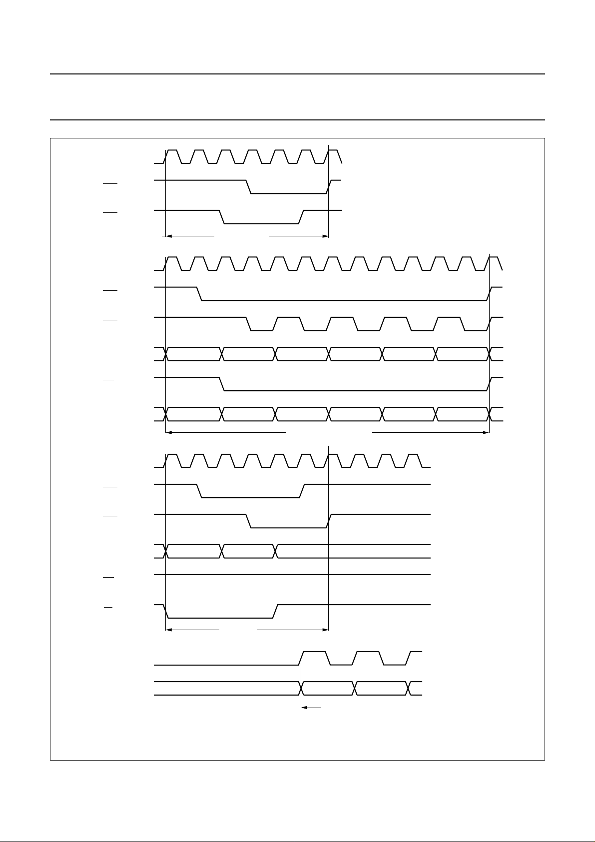
262144 words of 8-bit. An overview of the timing diagrams
is given in Fig.9.
1996 Aug 07 20
Page 21
Philips Semiconductors Preliminary specification
Picture-In-Picture (PIP) controller SAB9077H
handbook, full pagewidth
handbook, full pagewidth
H (external)
sync
field ID (internal)
(number of pixels)
V (external)
sync
V (external)
sync
43238943
1st field
MBE100
2nd field
Fig.7 Vertical synchronization timing and field identification.
BGHFP
BGVFP
DHFP
1 + VRPN rows
DVFP
VPIC
HPIC
1 + HRPN columns
Fig.8 Relation of display I2C-bus register.
1996 Aug 07 21
VDIS
HDIS
MGD583
Page 22
Philips Semiconductors Preliminary specification
Picture-In-Picture (PIP) controller SAB9077H
handbook, full pagewidth
CLOCK
RAS
CAS
CLOCK
RAS
CAS
AD0 to AD8
WE
DAO0 to DAO7
(1)
refresh cycle
(2)
ROW COLUMN COLUMN COLUMN COLUMN COLUMN
write cycle (main or sub)
(2)
CLOCK
RAS
CAS
AD0 to AD8
WE
DT
SC
DAI0 to DAI7
(1) CLOCK = 13.5 MHz.
(2) CLOCK = 27 MHz.
ROW COLUMN
read cycle
Fig.9 VDRAM timing.
shift clock cycles
MGC970
1996 Aug 07 22
Page 23
Philips Semiconductors Preliminary specification
Picture-In-Picture (PIP) controller SAB9077H
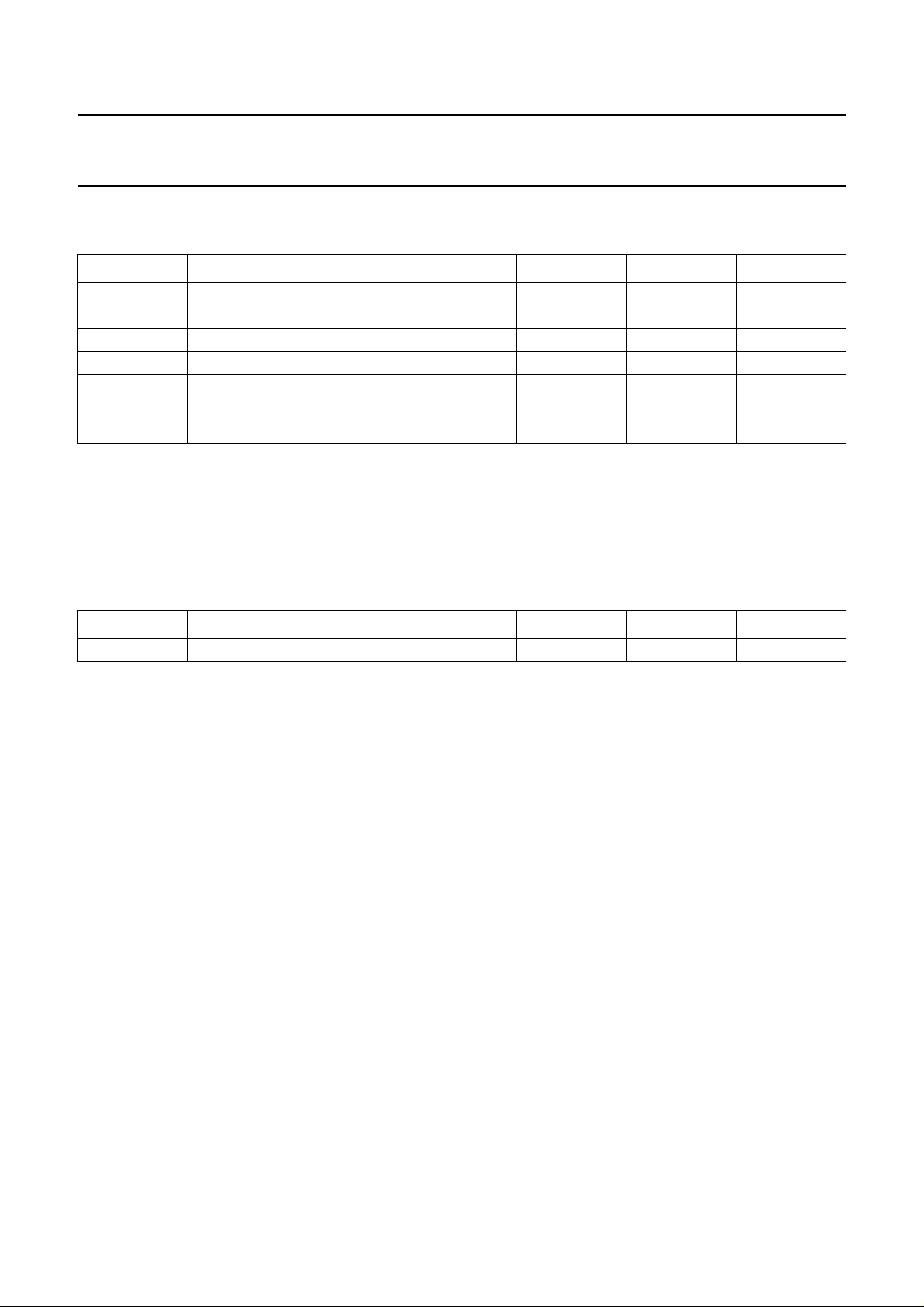
LIMITING VALUES
In accordance with the Absolute Maximum Rating System (IEC 134).
SYMBOL PARAMETER MIN. MAX. UNIT
V
DD
P
max
T
stg
T
amb
V
esd
Notes
1. Human body model: see
Reference Handbook”
2. Machine model: see
Reference Handbook”
supply voltage −0.5 +6.5 V
maximum power dissipation − 1.5 W
storage temperature −25 +150 °C
operating ambient temperature −25 +70 °C
electrostatic discharge handling
(2)
(1)
V
V
Human body model 3000
Machine model 300
“UZW-B0/FQ-B302”
; The numbers of the quality specification can be found in the
. The handbook can be ordered using the code 9397 750 00192.
“UZW-B0/FQ-A302”
; The numbers of the quality specification can be found in the
. The handbook can be ordered using the code 9397 750 00192.
“Quality
“Quality
THERMAL CHARACTERISTICS
SYMBOL PARAMETER CONDITIONS VALUE UNIT
R
th j-a
thermal resistance from junction to ambient in free air 34 K/W
QUALITY SPECIFICATION
In accordance with
“SNW-FQ-611 part E”
Reference Handbook”
. The handbook can be ordered using the code 9397 750 00192.
. The numbers of the quality specification can be found in the
“Quality
1996 Aug 07 23
Page 24
Philips Semiconductors Preliminary specification
Picture-In-Picture (PIP) controller SAB9077H
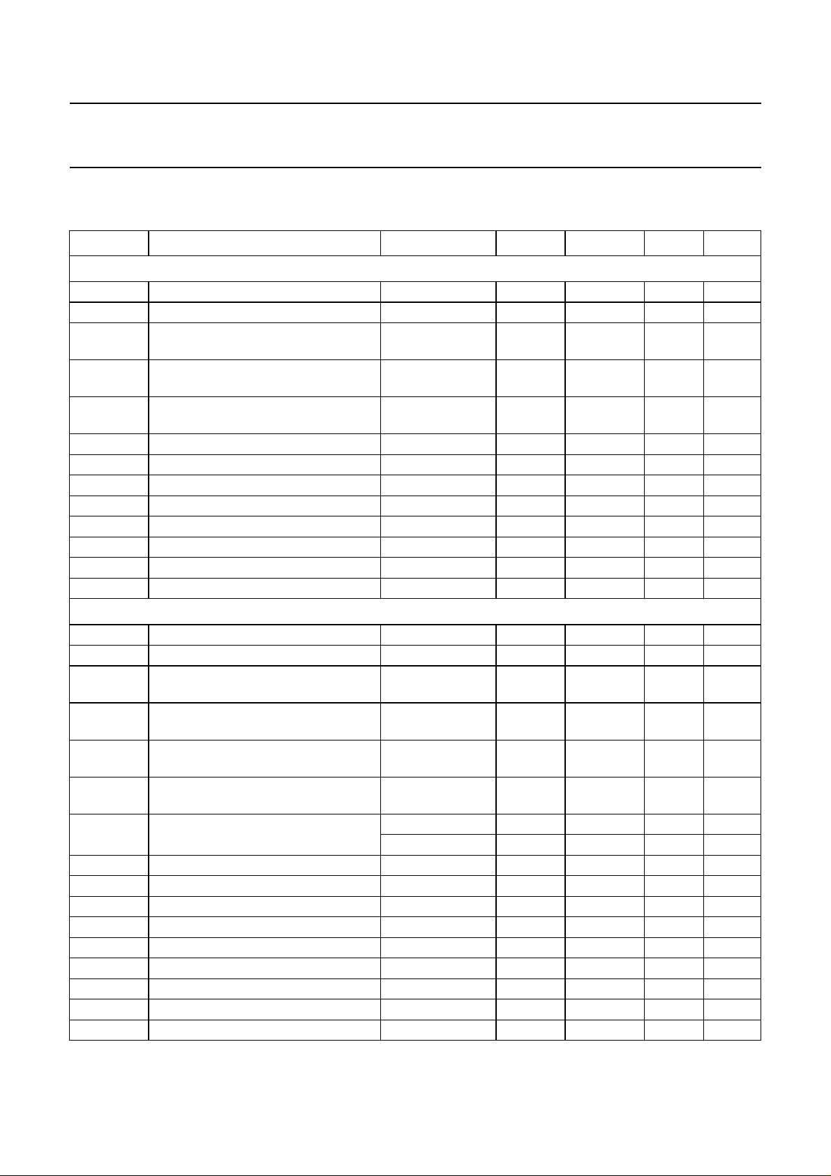
CHARACTERISTICS
= 5.0 V; T
V
DD
SYMBOL PARAMETER CONDITIONS MIN. TYP. MAX. UNIT
Supply
V
DD
V
SS
∆V
DD(max)
∆V
SS(max)
I
DDDQ
I
MPVDDA
I
SPVDDA
I
DPVDDA
I
MAVDDA
I
SAVDDA
I
DAVDDA
I
DDA(tot)
I
DDD(tot)
Analog-to-digital converter and clamping
V
refT
V
refB
V
i(Y)(p-p)
V
i(V)(p-p)
V
i(U)(p-p)
V
i(Y, U, V)(p-p)
I
i
C
i
f
s
RES resolution 6 8 − bit
DNL differential non-linearity −2.0 − +2.0 LSB
INL integral non-linearity −4.0 − +4.0 LSB
α
cs
PSRR power supply rejection ratio − 48 − dB
V
clampY
V
clampUV
=25°C; unless otherwise specified.
amb
all positive supply voltages 4.5 5.0 5.5 V
all ground voltages − 0 − V
maximum difference between supply
− 0 100 mV
voltages
maximum difference between ground
− 0 100 mV
voltages
quiescent current of digital supply
note 1 − 0 µA
voltages
main PLL supply current − 5 − mA
sub PLL supply current − 5 − mA
display PLL supply current − 5 − mA
main ADCs supply current − 40 − mA
sub ADCs supply current − 40 − mA
display DACs supply current − 20 − mA
total analog supply current − 115 − mA
total digital supply current − tbf − mA
top reference voltage note 2 1.9 2.1 2.3 V
bottom reference voltage note 2 0.3 0.4 0.5 V
input signal amplitude (peak-to-peak
TM2=VSS; note 2 0.80 1.00 1.10 V
value)
input signal amplitude (peak-to-peak
TM2=VSS; note 2 0.84 1.05 1.16 V
value)
input signal amplitude (peak-to-peak
TM2=VSS; note 2 1.06 1.33 1.50 V
value)
input signal amplitude (peak-to-peak
note 2 1.2 1.5 1.6 V
value)
input current clamping off − 0.1 −µA
clamping on − 100 −µA
input capacitance − 5 − pF
sample frequency rate note 3 − 1728H
sync
− MHz
channel separation − 48 − dB
clamping voltage level Y note 4 − V
refB
− V
clamping voltage level U/V note 4 − note 5 − V
1996 Aug 07 24
Page 25
Philips Semiconductors Preliminary specification
Picture-In-Picture (PIP) controller SAB9077H
SYMBOL PARAMETER CONDITIONS MIN. TYP. MAX. UNIT
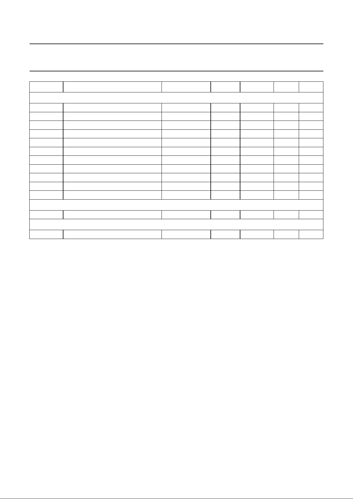
Digital-to-analog converter and output stage
V
refT
V
refB
V
o(Y, U, V)
R
L
C
L
f
s
RES resolution 6 8 8 bit
DNL differential non-linearity −1.0 − +1.0 LSB
INL integral non-linearity −1.0 − +1.0 LSB
α
cs
PSRR power supply rejection ratio − 48 − dB
PLL and clock generation acquisition
f
i(PLL)
PLL and clock generation display
f
i(PLL)
Notes
1. Digital clocks are silent, POR and TM
2. The V
V
refT
3. The internal system frequency is 1728 times the H
4. The Y-channel is clamped to the V
5. The UV-channel is clamped to1/2(V
6. The gain of the SAB9077H is 1 under the condition that the RL is 220 Ω.
top reference voltage 2.1 2.3 2.5 V
bottom reference voltage 0.3 0.4 0.5 V
output signal amplitude note 6 − 1.5 1.6 V
load resistance note 6 75 220 10 × 103Ω
load capacitance 0 − 50 pF
sample frequency rate note 3 − 1728Hsync − MHz
channel separation − 48 − dB
input frequency note 3 14 15.75 18 kHz
input frequency note 3 14 15.75 18 kHz
are connected to VDD.
2
refT
and V
AV
are made by a resistor division of the VDD. They can be calculated with the formulas
refB
2.0
× V= V
------- -
DD
5.0
and
AV
refB
of the ADCs.
refB
refT+VrefB+VLSB
DD
0.4
× V=
------- -
5.0
sync
input frequency for both the acquisition and display PLLs.
).
1996 Aug 07 25
Page 26
Philips Semiconductors Preliminary specification
Picture-In-Picture (PIP) controller SAB9077H
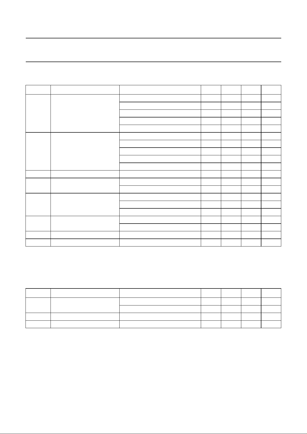
DC CHARACTERISTICS FOR THE DIGITAL PART
All V
pins = 4.5 to 5.5 V; T
DDD
SYMBOL PARAMETER CONDITIONS MIN. TYP. MAX. UNIT
V
IH
V
IL
V
hys
V
OH
V
OL
input leakage current HPF01; V
I
LI
I
3-state output leakage current IOI41; V
OZ
R
pu
HIGH level input voltage HPF01 70 −−%V
LOW level input voltage HPF01 −−30 %V
hysteresis voltage HUP07 − 33 − %V
HIGH level output voltage OPF20; IOL= −2 mA; V
LOW level output voltage IOI41; IOL= +2 mA; V
internal pull-up resistor HUP07 17 − 134 kΩ
= −20 to +75 °C; unless otherwise specified
amb
HPP01 70 −−%V
HUP07 80 −−%V
IOI41 70 −−%V
HOU21 70 −−%V
HPP01 −−30 %V
HUP07 −−20 %V
IOI41 −−30 %V
HOU21 −−30 %V
SPF20; I
OPF20; I
SPF20; I
HPP01; V
= −2 mA; V
OL
DDD
= +2 mA; V
OL
= +2 mA; V
OL
= 5.5 V; − 0.1 1 µA
DDD
= 5.5 V; − 0.1 1 µA
DDD
= 5.5 V − 0.2 5 µA
DDD
= 4.5 V 4.1 −−V
DDD
= 4.5 V 4.1 −−V
DDD
= 4.5 V −−0.4 V
= 4.5 V −−0.4 V
DDD
= 4.5 V −−0.4 V
DDD
DD
DD
DD
DD
DD
DD
DD
DD
DD
DD
DD
Note
is attached to the V
1. V
in
DDD
or V
SSD
.
AC CHARACTERISTICS FOR THE DIGITAL PART
V
= 4.5 to 5.5 V (all V
DDD
DDD
pins); T
= −20 to +75 °C; unless otherwise specified
amb
SYMBOL PARAMETER CONDITIONS MIN. TYP. MAX. UNIT
f
sys
system frequency acquisition; note 1 − 27 30 MHz
display; note 1 − 27 30 MHz
t
r
t
f
rise time − 625ns
fall time − 625ns
Notes
1. The internal system frequency is1728 times the H
input frequency for both the acquisition and display PLLs.
sync
1996 Aug 07 26
Page 27
Philips Semiconductors Preliminary specification
Picture-In-Picture (PIP) controller SAB9077H
TEST AND APPLICATION INFORMATION
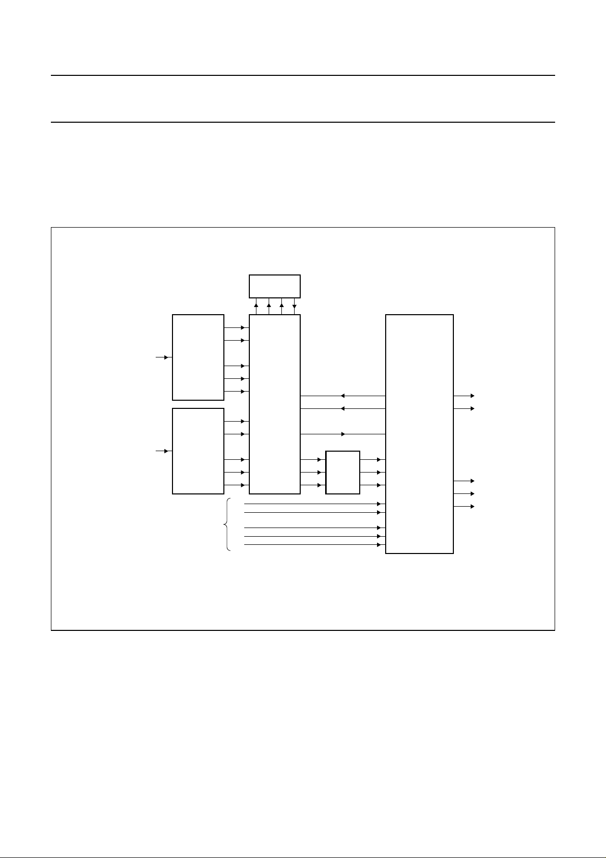
The application diagram for 1 FH mode in a standard
configuration is shown in Fig.10. Two input signals
MCVBS and SCVBS of different sources are processed by
the SAB9077H and inserted by the YUV/RGB switch.
handbook, full pagewidth
SCVBS
MCVBS
DECODER
SUB
DECODER
MAIN
main signals
HS
VS
HS
VS
Y
U
V
Y
U
V
HS
VS
Y
U
V
VDRAM
2 Mbit
SAB9077H
The synchronization of the display PLL is derived from the
deflection circuit. The main signals are also led to the
deflection circuit and the YUV/RGB switch where the
SAB9077H signals can be inserted. The signals for
deflection can also be taken from the main channel or
sub-channel decoder.
HS (1 FH)
VS
FLB
Y
U
V
YUV
TO
RGB
YUV/RGB SWITCH
DEFLECTION
R
G
B
CIRCUIT
AND
HS
VS
R
G
B
MBH504
Fig.10 Application diagram for 1 FH mode.
1996 Aug 07 27
Page 28
Philips Semiconductors Preliminary specification
Picture-In-Picture (PIP) controller SAB9077H
handbook, full pagewidth
TDA8310A
CVBS/Y
CVBS/Y
main-channel input
HOUT
VOUT
−V
−U
+5 V+5 V
97 98 91
bias
SSA
DPV
1
MPV
bias
99
+5 V
+5 V
Y
+5 V
+5 V
+5 V
100
17
10
11
12
14
13
15
16
18
63
19
20
21
22
4
3
2
5
8
9
6
7
MPV
MPV
MAV
MAV
MPH
MV
sync
MAV
MV
MAV
MU
MAV
MY
MAV
MAV
MV
DDD
MV
SSD
MCV
MCV
TDCLK
TACLK
TC
TM0
TM1
TM2
DAO0
36, 38,
8
39, 37,
35, 33
DDA
SSA
DDD
SSD
sync
bias
refB
refT
DDA
SSA
DDD
SSD
to DAO7
DDA
DPV
DPV
DAI0
to DAI7
23, 25,
27, 29,
8
30, 28,
26, 24
2 Mbit MEMORY
syncDVsync
DPH
SC
4032, 34,
DT
DFB
DAV
WE
92
SSD
DDD
DAV
SAB9077H
RAS
CAS
49484731
9
DU
DAV
DV
AD0 to AD8
51, 53,
55, 57,
58, 56,
54, 52,
50
refB
SSD
DV
+5 V
DDD
DV
4344
refT
DAV
DCV
DY
SSD
+5 V
bias
DAV
DDD
DCV
4241
SPV
SPV
SPV
SAV
SAV
SPH
SAV
SAV
SAV
SAV
SAV
SCV
SCV
84 8396 8995 94 93 90 8788 8586
SSA
DAV
SV
SV
SV
SSD
V
45
+5 V
bias
DDA
SSA
DDD
SSD
sync
sync
bias
SV
refB
SU
refT
SY
DDA
SSA
DDD
SSD
DDD
SSD
POR
SDA
SCL
+5 V
A0
DDA
DAV
DDD
V
46
80
82
81
77
78
79
64
76
73
72
75
74
71
70
69
67
68
66
65
62
61
60
59
MBH505
+5 V
+5 V
+5 V
+5 V
+5 V
HOUT
VOUT
−V
TDA8310A
−U
Y
CVBS/Y
CVBS/Y
sub-channel input
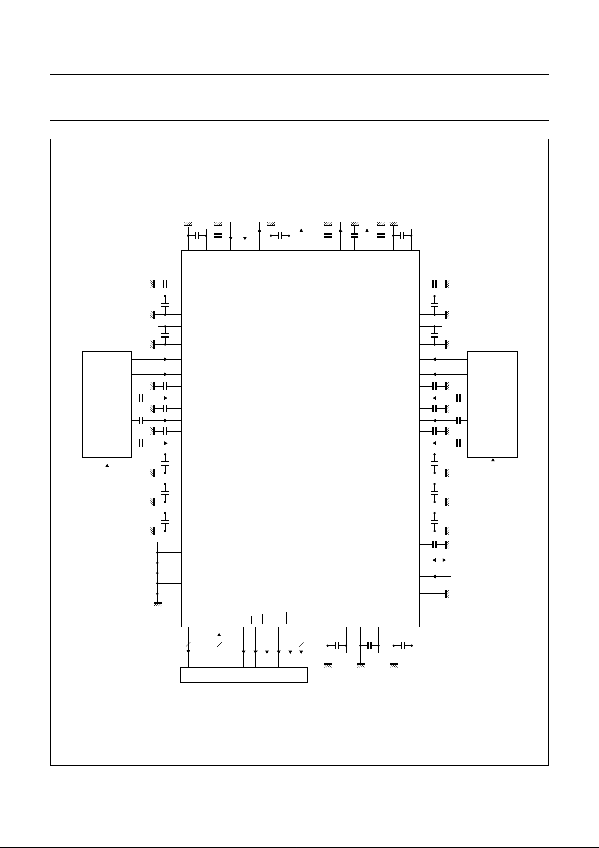
All capacitors are 100 nF.
On the application board a ground plane should be used.
Fig.11 Application diagram.
1996 Aug 07 28
Page 29
Philips Semiconductors Preliminary specification
Picture-In-Picture (PIP) controller SAB9077H
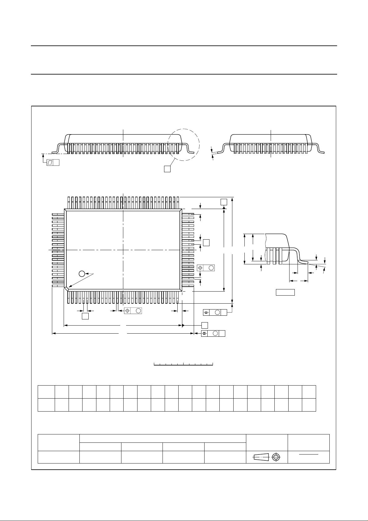
PACKAGE OUTLINE
QFP100: plastic quad flat package; 100 leads (lead length 1.95 mm); body 14 x 20 x 2.8 mm
c
y
X
E
e
w M
p
A
A
H
E
E
2
A
A
1
80 51
81
pin 1 index
100
1
50
Z
b
31
30
detail X
L
p
L
SOT317-2
(A )
3
θ
w M
b
e
p
Z
D
D
H
D
0 5 10 mm
scale
DIMENSIONS (mm are the original dimensions)
mm
A
max.
3.20
0.25
0.05
2.90
2.65
0.25
0.40
0.25
0.25
0.14
UNIT A1A2A3bpcE
(1)
(1) (1)(1)
D
20.1
19.9
eH
H
14.1
13.9
0.65
24.2
23.6
Note
1. Plastic or metal protrusions of 0.25 mm maximum per side are not included.
OUTLINE
VERSION
IEC JEDEC EIAJ
REFERENCES
SOT317-2
1996 Aug 07 29
D
B
E
18.2
17.6
v M
A
v M
B
LL
p
1.0
0.6
0.15 0.10.21.95
EUROPEAN
PROJECTION
Z
D
0.8
0.4
Zywv θ
E
o
1.0
7
o
0.6
0
ISSUE DATE
95-02-04
97-08-01
Page 30

Philips Semiconductors Preliminary specification
Picture-In-Picture (PIP) controller SAB9077H
SOLDERING
Introduction
There is no soldering method that is ideal for all IC
packages. Wave soldering is often preferred when
through-hole and surface mounted components are mixed
on one printed-circuit board. However, wave soldering is
not always suitable for surface mounted ICs, or for
printed-circuits with high population densities. In these
situations reflow soldering is often used.
This text gives a very brief insight to a complex technology.
A more in-depth account of soldering ICs can be found in
“IC Package Databook”
our
Reflow soldering
Reflow soldering techniques are suitable for all QFP
packages.
The choice of heating method may be influenced by larger
plastic QFP packages (44 leads, or more). If infrared or
vapour phase heating is used and the large packages are
not absolutely dry (less than 0.1% moisture content by
weight), vaporization of the small amount of moisture in
them can cause cracking of the plastic body. For more
information, refer to the Drypack chapter in our
Reference Handbook”
Reflow soldering requires solder paste (a suspension of
fine solder particles, flux and binding agent) to be applied
to the printed-circuit board by screen printing, stencilling or
pressure-syringe dispensing before package placement.
Several techniques exist for reflowing; for example,
thermal conduction by heated belt. Dwell times vary
between 50 and 300 seconds depending on heating
method. Typical reflow temperatures range from
215 to 250 °C.
(order code 9398 652 90011).
“Quality
(order code 9397 750 00192).
If wave soldering cannot be avoided, the following
conditions must be observed:
• A double-wave (a turbulent wave with high upward
pressure followed by a smooth laminar wave)
soldering technique should be used.
• The footprint must be at an angle of 45° to the board
direction and must incorporate solder thieves
downstream and at the side corners.
Even with these conditions, do not consider wave
soldering the following packages: QFP52 (SOT379-1),
QFP100 (SOT317-1), QFP100 (SOT317-2),
QFP100 (SOT382-1) or QFP160 (SOT322-1).
During placement and before soldering, the package must
be fixed with a droplet of adhesive. The adhesive can be
applied by screen printing, pin transfer or syringe
dispensing. The package can be soldered after the
adhesive is cured.
Maximum permissible solder temperature is 260 °C, and
maximum duration of package immersion in solder is
10 seconds, if cooled to less than 150 °C within
6 seconds. Typical dwell time is 4 seconds at 250 °C.
A mildly-activated flux will eliminate the need for removal
of corrosive residues in most applications.
Repairing soldered joints
Fix the component by first soldering two diagonallyopposite end leads. Use only a low voltage soldering iron
(less than 24 V) applied to the flat part of the lead. Contact
time must be limited to 10 seconds at up to 300 °C. When
using a dedicated tool, all other leads can be soldered in
one operation within 2 to 5 seconds between
270 and 320 °C.
Preheating is necessary to dry the paste and evaporate
the binding agent. Preheating duration: 45 minutes at
45 °C.
Wave soldering
Wave soldering is not recommended for QFP packages.
This is because of the likelihood of solder bridging due to
closely-spaced leads and the possibility of incomplete
solder penetration in multi-lead devices.
1996 Aug 07 30
Page 31
Philips Semiconductors Preliminary specification
Picture-In-Picture (PIP) controller SAB9077H
DEFINITIONS
Data sheet status
Objective specification This data sheet contains target or goal specifications for product development.
Preliminary specification This data sheet contains preliminary data; supplementary data may be published later.
Product specification This data sheet contains final product specifications.
Limiting values
Limiting values given are in accordance with the Absolute Maximum Rating System (IEC 134). Stress above one or
more of the limiting values may cause permanent damage to the device. These are stress ratings only and operation
of the device at these or at any other conditions above those given in the Characteristics sections of the specification
is not implied. Exposure to limiting values for extended periods may affect device reliability.
Application information
Where application information is given, it is advisory and does not form part of the specification.
LIFE SUPPORT APPLICATIONS
These products are not designed for use in life support appliances, devices, or systems where malfunction of these
products can reasonably be expected to result in personal injury. Philips customers using or selling these products for
use in such applications do so at their own risk and agree to fully indemnify Philips for any damages resulting from such
improper use or sale.
2
PURCHASE OF PHILIPS I
C COMPONENTS
2
Purchase of Philips I
components in the I2C system provided the system conforms to the I2C specification defined by
Philips. This specification can be ordered using the code 9398 393 40011.
C components conveys a license under the Philips’ I2C patent to use the
1996 Aug 07 31
Page 32

Philips Semiconductors – a worldwide company
Argentina: see South America
Australia: 34 Waterloo Road, NORTH RYDE, NSW 2113,
Tel. +61 2 9805 4455, Fax. +61 2 9805 4466
Austria: Computerstr. 6, A-1101 WIEN, P.O. Box 213,
Tel. +43 1 60 101, Fax. +43 1 60 101 1210
Belarus: Hotel Minsk Business Center, Bld. 3, r. 1211, Volodarski Str. 6,
220050 MINSK, Tel. +375 172 200 733, Fax. +375 172 200 773
Belgium: see The Netherlands
Brazil: seeSouth America
Bulgaria: Philips Bulgaria Ltd., Energoproject, 15thfloor,
51 James Bourchier Blvd., 1407 SOFIA,
Tel. +359 2 689 211, Fax. +359 2 689 102
Canada: PHILIPS SEMICONDUCTORS/COMPONENTS,
Tel. +1 800 234 7381
China/Hong Kong: 501 Hong Kong Industrial Technology Centre,
72 Tat Chee Avenue, Kowloon Tong, HONG KONG,
Tel. +852 2319 7888, Fax. +852 2319 7700
Colombia: see South America
Czech Republic: see Austria
Denmark: Prags Boulevard 80, PB 1919, DK-2300 COPENHAGEN S,
Tel. +45 32 88 2636, Fax. +45 31 57 1949
Finland: Sinikalliontie 3, FIN-02630 ESPOO,
Tel. +358 615 800, Fax. +358 615 80920
France: 4 Rue du Port-aux-Vins, BP317, 92156 SURESNES Cedex,
Tel. +33 1 40 99 6161, Fax. +33 1 40 99 6427
Germany: Hammerbrookstraße 69, D-20097 HAMBURG,
Tel. +49 40 23 53 60, Fax. +49 40 23 536 300
Greece: No. 15, 25th March Street, GR 17778 TAVROS,
Tel. +30 1 4894 339/911, Fax. +30 1 4814 240
Hungary: seeAustria
India: Philips INDIA Ltd, Shivsagar Estate, A Block, Dr. Annie Besant Rd.
Worli, MUMBAI 400 018, Tel. +91 22 4938 541, Fax. +91 22 4938 722
Indonesia: see Singapore
Ireland: Newstead, Clonskeagh, DUBLIN 14,
Tel. +353 1 7640 000, Fax. +353 1 7640 200
Israel: RAPAC Electronics, 7 Kehilat Saloniki St, TEL AVIV 61180,
Tel. +972 3 645 0444, Fax. +972 3 649 1007
Italy: PHILIPS SEMICONDUCTORS, Piazza IV Novembre 3,
20124 MILANO, Tel. +39 2 6752 2531, Fax. +39 2 6752 2557
Japan: Philips Bldg 13-37, Kohnan 2-chome, Minato-ku, TOKYO 108,
Tel. +81 3 3740 5130, Fax. +81 3 3740 5077
Korea: Philips House, 260-199 Itaewon-dong, Yongsan-ku, SEOUL,
Tel. +82 2 709 1412, Fax. +82 2 709 1415
Malaysia: No. 76 Jalan Universiti, 46200 PETALING JAYA, SELANGOR,
Tel. +60 3 750 5214, Fax. +60 3 757 4880
Mexico: 5900 Gateway East, Suite 200, EL PASO, TEXAS 79905,
Tel. +9-5 800 234 7381
Middle East: see Italy
Netherlands: Postbus 90050, 5600 PB EINDHOVEN, Bldg. VB,
Tel. +31 40 27 82785, Fax. +31 40 27 88399
New Zealand: 2 Wagener Place, C.P.O. Box 1041, AUCKLAND,
Tel. +64 9 849 4160, Fax. +64 9 849 7811
Norway: Box 1, Manglerud 0612, OSLO,
Tel. +47 22 74 8000, Fax. +47 22 74 8341
Philippines: Philips Semiconductors Philippines Inc.,
106 Valero St. Salcedo Village, P.O. Box 2108 MCC, MAKATI,
Metro MANILA, Tel. +63 2 816 6380, Fax. +63 2 817 3474
Poland: Ul. Lukiska 10, PL 04-123 WARSZAWA,
Tel. +48 22 612 2831, Fax. +48 22 612 2327
Portugal: see Spain
Romania: see Italy
Russia: Philips Russia, Ul. Usatcheva 35A, 119048 MOSCOW,
Tel. +7 095 926 5361, Fax. +7 095 564 8323
Singapore: Lorong 1, Toa Payoh, SINGAPORE 1231,
Tel. +65 350 2538, Fax. +65 251 6500
Slovakia: see Austria
Slovenia: see Italy
South Africa: S.A. PHILIPS Pty Ltd., 195-215 Main Road Martindale,
2092 JOHANNESBURG, P.O. Box 7430 Johannesburg 2000,
Tel. +27 11 470 5911, Fax. +27 11 470 5494
South America: Rua do Rocio 220, 5th floor, Suite 51,
04552-903 São Paulo, SÃO PAULO - SP, Brazil,
Tel. +55 11 821 2333, Fax. +55 11 829 1849
Spain: Balmes 22, 08007 BARCELONA,
Tel. +34 3 301 6312, Fax. +34 3 301 4107
Sweden: Kottbygatan 7, Akalla, S-16485 STOCKHOLM,
Tel. +46 8 632 2000, Fax. +46 8 632 2745
Switzerland: Allmendstrasse 140, CH-8027 ZÜRICH,
Tel. +41 1 488 2686, Fax. +41 1 481 7730
Taiwan: PHILIPS TAIWAN Ltd., 23-30F, 66,
Chung Hsiao West Road, Sec. 1, P.O. Box 22978,
TAIPEI 100, Tel. +886 2 382 4443, Fax. +886 2 382 4444
Thailand: PHILIPS ELECTRONICS (THAILAND) Ltd.,
209/2 Sanpavuth-Bangna Road Prakanong, BANGKOK 10260,
Tel. +66 2 745 4090, Fax. +66 2 398 0793
Turkey: Talatpasa Cad. No. 5, 80640 GÜLTEPE/ISTANBUL,
Tel. +90 212 279 2770, Fax. +90 212 282 6707
Ukraine: PHILIPS UKRAINE, 4 Patrice Lumumba str., Building B, Floor 7,
252042 KIEV, Tel. +380 44 264 2776, Fax. +380 44 268 0461
United Kingdom: Philips Semiconductors Ltd., 276 Bath Road, Hayes,
MIDDLESEX UB3 5BX, Tel. +44 181 730 5000, Fax. +44 181 754 8421
United States: 811 East Arques Avenue, SUNNYVALE, CA 94088-3409,
Tel. +1 800 234 7381
Uruguay: see South America
Vietnam: see Singapore
Yugoslavia: PHILIPS, Trg N. Pasica 5/v, 11000 BEOGRAD,
Tel. +381 11 825 344, Fax.+381 11 635 777
For all other countries apply to: Philips Semiconductors, Marketing & Sales Communications,
Building BE-p, P.O. Box 218, 5600 MD EINDHOVEN, The Netherlands, Fax. +31 40 27 24825
© Philips Electronics N.V. 1996 SCA51
All rights are reserved. Reproduction in whole or in part is prohibited without the prior written consent of the copyright owner.
The information presented in this document does not form part of any quotation or contract, is believed to be accurate and reliable and may be changed
without notice. No liability will be accepted by the publisher for any consequence of its use. Publication thereof does not convey nor imply any license
under patent- or other industrial or intellectual property rights.
Internet: http://www.semiconductors.philips.com
Printed in The Netherlands 537021/50/01/pp32 Date of release: 1996 Aug 07 Document order number: 9397 750 01003
 Loading...