

Datasheet SAB80C535-16-N-T40-85, SAB80C535-20-N, SAB80C535-M, SAB80C535-M-T40-85, SAB80C535-N Datasheet (Siemens)
...Page 1

Data Sheet 02.96
Microcomputer Components
SAB 80C515 / SAB 80C535
8-Bit CMOS Single-Chip Microcontroller
Page 2

Semiconductor Group 1 02.96
High-Performance
8-Bit CMOS Single-Chip Microcontroller SAB 80C515/80C535
Preliminary
SAB 80C515/80C515-16 CMOS microcontroller with factory mask-programmable ROM
SAB 80C535/80C535-16 CMOS microcontroller for external ROM
● 8 K × 8 ROM (SAB 80C515 only) ● Boolean processor
● 256 × 8 RAM ● Most instructions execute in 1 µs (750 ns)
● Six 8-bit I/O ports, one input port for ● 4 µs (3 µs) multiply and divide
digital or analog input
● External memory expandable up to
● Three 16-bit timer/counters 128 Kbytes
● Highly flexible reload, capture, compare ● Backwardly compatible with SAB 8051
capabilities
● Functionally compatible with SAB 80515
● Full-duplex serial channel ● Idle and power-down mode
● Twelve interrupt vectors, four priority ● Plastic leaded chip carrier package:
levels P-LCC-68
● 8-bit A/D converter with 8 multiplexed ● Plastic Metric Quad Flat Package
inputs and programmable internal P-MQFP-80
reference voltages
● Two temperature ranges available:
● 16-bit watchdog timer 0 to 70 ˚C (for 12, 16, 20 MHz)
– 40 to 85 ˚C (for 12, 16 MHz)
The SAB 80C515/80C535 is a powerful member of the Siemens SAB 8051 family
of 8-bit microcontrollers. It is designed in Siemens ACMOS technology and is functionally
compatible with the SAB 80515/80535 devices designed in MYMOS technology.
The SAB 80C515/80C535 is a stand-alone, high-performance single-chip microcontroller
based on the SAB 8051/80C51 architecture. While maintaining all the SAB 80C51 operating
characteristics, the SAB 80C515/80C535 incorporates several enhancements which
significantly increase design flexibility and overall system performance.
In addition, the low-power properties of Siemens ACMOS technology allow applications where
power consumption and dissipation are critical. Furthermore, the SAB 80C515/80C535 has
two software-selectable modes of reduced activity for further power reduction: idle and powerdown mode.
The SAB 80C535 is identical with the SAB 80C515 except that it lacks the on-chip program
memory. The SAB 80C515/80C535 is supplied in a 68-pin plastic leaded chip carrier package
(P-LCC-68) or in a plastic metric quad flat package (P-MQFP-80).
There are versions for 12, 16 and 20 MHz operation and for 16 MHz operation and for extended
temperature ranges – 40 to 85 ˚C. Versions for extended temperature range – 40 to + 110 ˚C
are available on request.
Page 3

SAB 80C515/80C535
Semiconductor Group 2
Page 4

SAB 80C515/80C535
Semiconductor Group 3
Notes: Versions for extended temperature range – 40 to + 110 ˚C on request.
The ordering number of ROM types (DXXXX extension) is defined after program release
(verification) of the customer.
Ordering Information
Type Ordering
Code
Package Description
8-Bit CMOS Microcontroller
SAB 80C515-N Q67120-DXXXX P-LCC-68 with mask-programmable ROM,
12 MHz
SAB 80C535-N Q67120-C0508 P-LCC-68 for external memory, 12 MHz
SAB 80C515-N-T40/85 Q67120-DXXXX P-LCC-68 with mask-programmable ROM,
12 MHz
ext. temperature – 40 to + 85 ˚C
SAB 80C535-N-T40/85 Q67120-C0510 P-LCC-68 for external memory, 12 MHz
ext. temperature – 40 to + 85 ˚C
SAB 80C515-16-N Q67120-DXXXX P-LCC-68 with mask-programmable ROM,
16 MHz
SAB 80C535-16-N Q67120-C0509 P-LCC-68 for external memory, 16 MHz
SAB 80C535-16-N-
T40/85
Q67120-C0562 P-LCC-68 for external memory, 16 MHz
ext. temperature – 40 to + 85 ˚C
SAB 80C535-20-N Q67120-C0778 P-LCC-68 for external memory, 20 MHz
SAB 80C535-M Q67120-C0857 P-MQFP-80 for external memory, 12 MHz
SAB 80C515-M Q67120-DXXXX P-MQFP-80 with mask-programmable ROM,
12 MHz
SAB 80C535-M-T40/85 Q67120-C0937 P-MQFP-80 for external memory, 12 MHz
ext. temperature – 40 to + 85 ˚C
SAB 80C515-M-T40/85 Q67120-DXXXX P-MQFP-80 with mask-programmable ROM,
12 MHz
ext. temperature – 40 to + 85 ˚C
Page 5

SAB 80C515/80C535
Semiconductor Group 4
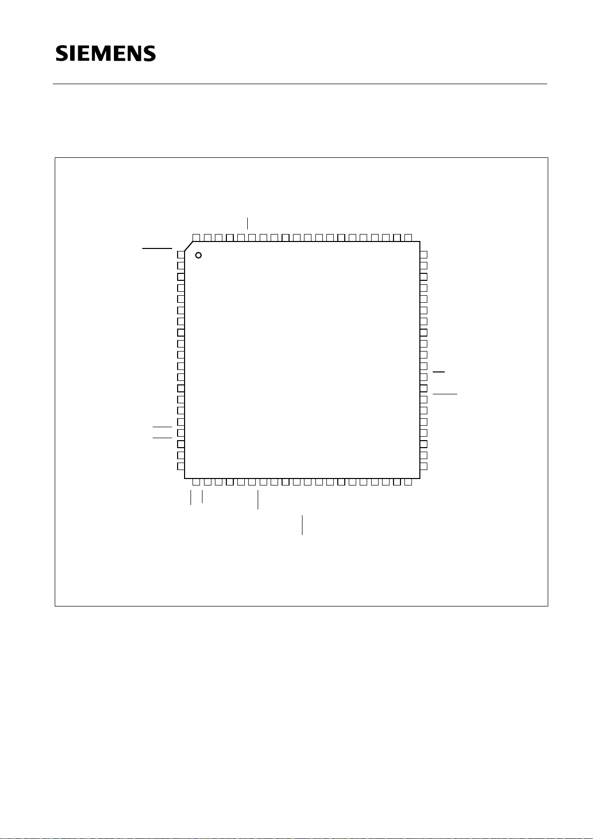
Pin Configuration
(top view)
P-LCC-68
Page 6
SAB 80C515/80C535
Semiconductor Group 5
Pin Configuration
(top view)
N.C. pins must not be connected.
P0.6 / AD6
SAB 80C535 / 80C515
80
1
P-MQFP-80
Package
5
10
15
20
21 25 30
40
41
35
45
50
55
60
61
657075
P0.7 / AD7
P0.5 / AD5
P0.4 / AD4
P0.2 / AD2
P0.3 / AD3
P0.1 / AD1
P0.0 / AD0
P5.7
N.C.
EA
ALE
PSEN
P2.7 / A15
N.C.
N.C.
P2.6 / A14
P2.5 / A13
P2.4 / A12
P2.3 / A11
VAREF
N.C.
VAGND
P6.7 / AIN7
P6.5 / AIN5
P6.6 / AIN6
P6.4 / AIN4
P6.3 / AIN3
RESET
P6.2 / AIN2
P6.0 / AIN0
N.C.
N.C.
P3.1 / TXD0
P6.1 / AIN1
P3.0 / RXD0
P3.2 /
INT0
P3.3 /
INT1
P3.4 / T0
P3.5 / T1
N.C.
P3.7 /
RD
P1.7 / T2
P1.6 / CLKOUT
P1.4 /
INT2
P1.5 / T2EX
P1.3 / INT6 / CC3
P1.2 / INT5 / CC2
P3.6 /
WR
P1.1 / INT4 / CC1
N.C.
VCC
VSS
XTAL2
P1.0 /
INT3 / CC0
N.C.
XTAL1
P2.0 / A8
P2.1 / A9
P2.2 / A10
P4.5
P4.6
P4.4
P4.3
P4.2
PE
P4.1
P4.0
P4.7
N.C.
VCC
N.C.
P5.0
P5.2
N.C.
P5.1
P5.3
P5.4
P5.5
P5.6
P-MQFP-80
Page 7

SAB 80C515/80C535
Semiconductor Group 6
Logic Symbol
Page 8

SAB 80C515/80C535
Semiconductor Group 7
Pin Definitions and Functions
Symbol Pin
P-LCC-68
Pin
P-MQFP-80
Input (I)
Output (O)
Function
P4.0-P4.7 1-3, 5-9 72-74,
76-80
I/O Port 4
is an 8-bit bidirectional I/O port with
internal pullup resistors. Port 4 pins that
have 1’s written to them are pulled high by
the internal pullup resistors, and in that
state can be used as inputs. As inputs,
port 4 pins being externally pulled low will
source current (I
I L
,
in the DC
characteristics) because of the internal
pullup resistors.
PE 4 75 I Power saving mode enable
A low level on this pin enables the use of
the power saving modes (idle mode and
power-down mode). When
PE is held on
high level it is impossible to enter the
power saving modes.
RESET 10 1 I Reset pin
A low level on this pin for the duration of
two machine cycles while the oscillator is
running resets the SAB 80C515. A small
internal pullup resistor permits power-on
reset using only a capacitor connected
to V
SS
.
V
AREF
11 3 Reference voltage for the A/D converter
V
AGND
12 4 Reference ground for the A/D converter
P6.7-P6.0 13-20 5-12 Port 6
is an 8-bit undirectional input port. Port
pins can be used for digital input if voltage
levels simultaneously meet the
specifications for high/low input voltages
and for the eight multiplexed analog inputs
of the A/D converter.
Page 9
SAB 80C515/80C535
Semiconductor Group 8
Pin Definitions and Functions (cont’d)
Symbol Pin
P-LCC-68
Pin
P-MQFP-80
Input (I)
Output (O)
Function
P3.0-P3.7 21-28 15-22 I/O Port 3
is an 8-bit bidirectional I/O port with
internal pullup resistors. Port 3 pins that
have1's written to them are pulled high by
the internal pullup resistors, and in that
state can be used as inputs. As inputs,
port 3 pins being externally pulled low will
source current (I
IL
, in the DC
characteristics) because of the internal
pullup resistors. Port 3 also contains the
interrupt, timer, serial port and external
memory strobe pins that are used by
various options. The output latch
corresponding to a secondary function
must be programmed to a one (1) for that
function to operate. The secondary
functions are assigned to the pins of port
3, as follows:
–R
×D (P3.0): serial port's receiver data
input (asynchronous) or data input/
output (synchronous)
–T
×D (P3.1): serial port's transmitter data
output
(asynchronous) or clock output
(synchronous)
–I
NT0 (P3.2): interrupt 0 input/timer 0
gate control input
–
INT1 (P3.3): interrupt 1 input/timer 1
gate control input
– T0 (P3.4): counter 0 input
– T1 (P3.5): counter 1 input
–
WR (P3.6): the write control signal
latches the data byte from port 0 into the
external data memory
–
RD (P3.7): the read control signal
enables the external data memory to
port 0
Page 10
SAB 80C515/80C535
Semiconductor Group 9
P1.7-P1.0 29-36 24-31 I/O Port 1
is an 8-bit bidirectional I/O port with
internal pullup resistors. Port 1 pins that
have 1's written to them are pulled high by
the internal pullup resistors, and in that
state can be used as inputs. As inputs,
port 1 pins being externally pulled low will
source current (I
I L
in the DC
characteristics) because of the internal
pullup resistors. The port is used for the
low-order address byte during program
verification. Port 1 also contains the
interrupt, timer, clock, capture and
compare pins that are used by various
options. The output latch corresponding to
a secondary function must be
programmed to a one (1) for that function
to operate (except when used for the
compare functions). The secondary
functions are assigned to the port 1 pins
as follows:
–
INT3/CC0 (P1.0): interrupt 3 input/
compare 0 output/capture 0 input
– INT4/CC1 (P1.1): interrupt 4 input/
compare 1 output/capture 1 input
– INT5/CC2 (P1.2): interrupt 5 input/
compare 2 output/capture 2 input
– INT6/CC3 (P1.3): interrupt 6 input/
compare 3 output/capture 3 input
– INT2 (P1.4): interrupt 2 input
– T2EX (P1.5): timer 2 external reload
trigger input
– CLKOUT (P1.6): system clock output
– T2 (P1.7): counter 2 input
Pin Definitions and Functions (cont’d)
Symbol Pin
P-LCC-68
Pin
P-MQFP-80
Input (I)
Output (O)
Function
Page 11

SAB 80C515/80C535
Semiconductor Group 10
XTAL2
XTAL1
39
40
36
37
XTAL2
Input to the inverting oscillator amplifier
and input to the internal clock generator
circuits.
XTAL1
Output of the inverting oscillator amplifier.
To drive the device from an external clock
source, XTAL2 should be driven, while
XTAL1 is left unconnected. There are no
requirements on the duty cycle of the
external clock signal, since the input to the
internal clocking circuitry is divided down
by a divide-by-two flip-flop. Minimum and
maximum high and low times and rise/fall
times specified in the AC characteristics
must be observed.
P2.0-P2.7 41-48 38-45 I/O Port 2
is an 8-bit bidirectional I/O port with
internal pullup resistors. Port 2 pins that
have 1's written to them are pulled high by
the internal pullup resistors, and in that
state can be used as inputs. As inputs,
port 2 pins being externally pulled low will
source current (I
I L,
in the DC
characteristics) because of the internal
pullup resistors.
Port 2 emits the high-order address byte
during fetches from external program
memory and during accesses to external
data memory that use 16-bit addresses
(MOVX@DPTR). In this application it
uses strong internal pullup resistors when
issuing 1's. During accesses to external
data memory that use 8-bit addresses
(MOVX@Ri), port 2 issues the contents of
the P2 special function register.
Pin Definitions and Functions (cont’d)
Symbol Pin
P-LCC-68
Pin
P-MQFP-80
Input (I)
Output (O)
Function
Page 12

SAB 80C515/80C535
Semiconductor Group 11
PSEN 49 47 O The Program store enable
output is a control signal that enables the
external program memory to the bus
during external fetch operations. It is
activated every six oscillator periods,
except during external data memory
accesses. The signal remains high during
internal program execution.
ALE 50 48 O The Address latch enable
output is used for latching the address into
external memory during normal operation.
It is activated every six oscillator periods,
except during an external data memory
access.
EA 51 49 I External access enable
When held high, the SAB 80C515
executes instructions from the internal
ROM as long as the PC is less than 8192.
When held low, the SAB 80C515 fetches
all instructions from external program
memory. For the SAB 80C535 this pin
must be tied low.
P0.0-P0.7 52-59 52-59 I/O Port 0
is an 8-bit open-drain bidirectional I/O
port.
Port 0 pins that have 1's written to them
float, and in that state can be used as
high-impedance inputs.
Port 0 is also the multiplexed low-order
address and data bus during accesses to
external program and data memory. In
this application it uses strong internal
pullup resistors when issuing 1's.
Port 0 also outputs the code bytes during
program verification in the SAB 80C515.
External pullup resistors are required
during program verification.
Pin Definitions and Functions (cont’d)
Symbol Pin
P-LCC-68
Pin
P-MQFP-80
Input (I)
Output (O)
Function
Page 13

SAB 80C515/80C535
Semiconductor Group 12
P5.7-P5.0 60-67 60-67 I/O Port 5 is an 8-bit bidirectional I/O port with
internal pullup resistors. Port 5 pins that
have 1's written to them are pulled high by
the internal pullup resistors, and in that
state can be used as inputs. As inputs,
port 5 pins being externally pulled low will
source current
(I
IL
in the DC characteristics) because of
the internal pullup resistors.
V
CC
37 33 – Supply voltage
during normal, idle, and power-down
operation. Internally connected to pin 68.
V
SS
38 34 – Ground (0 V)
V
CC
68 69 – Supply voltage
during normal, idle, and power-down
operation. Internally connected to pin 37.
N. C. – 2, 13, 14,
23, 32, 35,
46, 50, 51,
68, 70, 71
– Not connected
These pins of the P-MQFP-80 package
must not be connected
Pin Definitions and Functions (cont’d)
Symbol Pin
P-LCC-68
Pin
P-MQFP-80
Input (I)
Output (O)
Function
Page 14

SAB 80C515/80C535
Semiconductor Group 13
Figure 1
Block Diagram
Page 15

SAB 80C515/80C535
Semiconductor Group 14
Functional Description
The members of the SAB 80515 family of microcontrollers are:
– SAB 80C515: Microcontroller, designed in Siemens ACMOS technology, with
8 Kbyte factory mask-programmable ROM
– SAB 80C535: ROM-less version of the SAB 80C515
– SAB 80515: Microcontroller, designed in Siemens MYMOS technology, with
8 Kbyte factory mask-programmable ROM
– SAB 80535: ROM-less version of the SAB 80515
The SAB 80C535 is identical to the SAB 80C515, except that it lacks the on-chip ROM.
In this data sheet the term "SAB 80C515" is used to refer to both the SAB 80C515 and
SAB 80C535, unless otherwise noted.
Principles of Architecture
The architecture of the SAB 80C515 is based on the SAB 8051/SAB 80C51 microcontroller
family. The following features of the SAB 80C515 are fully compatible with the SAB 80C51
features:
– Instruction set
– External memory expansion interface (port 0 and port 2)
– Full-duplex serial port
– Timer/counter 0 and 1
– Alternate functions on port 3
– The lower 128 bytes of internal RAM and the lower 4 Kbytes of internal ROM
The SAB 80C515 additionally contains 128 bytes of internal RAM and 4 Kbytes of internal
ROM, which results in a total of 256 bytes of RAM and 8 Kbytes of ROM on-chip.
The SAB 80C515 has a new 16-bit timer/counter with a 2:1 prescaler, reload mode, compare
and capture capability. It also contains at 16-bit watchdog timer, an 8-bit A/D converter with programmable reference voltages, two additional quasi-bidirectional 8-bit ports, one 8-bit input
port for analog or digital signals, and a programmable clock output (f
OSC
/12).
Furthermore, the SAB 80C515 has a powerful interrupt structure with 12 vectors and 4 programmable priority levels.
Figure 1 shows a block diagram of the SAB 80C515.
Page 16

SAB 80C515/80C535
Semiconductor Group 15
CPU
The SAB 80C515 is efficient both as a controller and as an arithmetic processor. It has
extensive facilities for binary and BCD arithmetic and excels in its bit-handling capabilities.
Efficient use of program memory results from an instruction set consisting of 44 % one-byte,
41 % two-byte, and 15 % three-byte instructions. With a 12 MHz crystal, 58 % of the
instructions execute in 1.0
µs.
Memory Organization
The SAB 80C515 manipulates operands in the four memory address spaces described below:
Figure 1 illustrates the memory address spaces of the SAB 80C515.
Program Memory
The SAB 80C515 has 8 Kbyte of on-chip ROM, while the SAB 80C535 has no internal ROM.
The program memory can be externally expanded up to 64 Kbytes. If the
EA pin is held high,
the SAB 80C515 executes out of internal ROM unless the address exceeds 1FFF
H
. Locations
2000H through 0FFFFH are then fetched from the external program memory. If the EA pin is
held now, the SAB 80C515 fetches all instructions from the external program memory. Since
the SAB 80C535 has no internal ROM, pin
EA must be tied low when using this component.
Data Memory
The data memory address space consists of an internal and an external memory space. The
internal data memory is divided into three physically separate and distinct blocks:
the lower 128 bytes of RAM, the upper 128 bytes of RAM, and the 128 byte special function
register (SRF) area. While the upper 128 bytes of data memory and the SFR area share the
same address locations, they are accessed through different addressing modes. The lower
128 bytes of data memory can be accessed through direct or register indirect addressing; the
upper 128 bytes of RAM can be accessed through register indirect addressing; the special
function registers are accessible through direct addressing.
Four 8-register banks, each bank consisting of eight 8-bit multi-purpose registers, occupy locations 0 through 1F
H
in the lower RAM area. The next 16 bytes, locations 20H through 2FH, contain 128 directly addressable bit locations. The stack can be located anywhere in the internal
data memory address space, and the stack depth can be expanded up to 256 bytes.
The external data memory can be expanded up to 64 Kbytes and can be accessed by instructions that use a 16-bit or an 8-bit address.
Page 17

SAB 80C515/80C535
Semiconductor Group 16
Figure 2
Memory Address Spaces
Page 18

SAB 80C515/80C535
Semiconductor Group 17
Special Function Registers
All registers, except the program counter and the four general purpose register banks, reside
in the special function register area. The special function registers include arithmetic registers,
pointers, and registers that provide an interface between the CPU and the on-chip peripherals.
There are also 128 directly addressable bits within the SFR area. All special function registers
are listed in table 1 and table 2.
In table 1 they are organized in numeric order of their addresses. In table 3 they are organized
in groups which refer to the functional blocks of the SAB 80C515.
Table 1
Special Function Register
Address Register Contents
after Reset
Address Register Contents
after Reset
80
H
81
H
82
H
83
H
84
H
85
H
86
H
87
H
P0
1)
SP
DPL
DPH
reserved
reserved
reserved
PCON
0FF
H
07
H
00
H
00
H
XX
H
2)
XX
H
2)
XX
H
2)
000X 0000
B
2)
98
H
99
H
9A
H
9B
H
9C
H
9D
H
9E
H
9F
H
SCON
1)
SBUF
reserved
reserved
reserved
reserved
reserved
reserved
00
H
XX
H
2)
XX
H
2)
XX
H
2)
XX
H
2)
XX
H
2)
XX
H
2)
XX
H
2)
88
H
89
H
8A
H
8B
H
8C
H
8D
H
8E
H
8F
H
TCON
1)
TMOD
TL0
TL1
TH0
TH1
reserved
reserved
00
H
00
H
00
H
00
H
00
H
00
H
XX
H
2)
XX
H
2)
A0
H
A1
H
A2
H
A3
H
A4
H
A5
H
A6
H
A7
H
P2
1)
reserved
reserved
reserved
reserved
reserved
reserved
reserved
0FF
H
XX
H
2)
XX
H
2)
XX
H
2)
XX
H
2)
XX
H
2)
XX
H
2)
XX
H
2)
90
H
91
H
92
H
93
H
94
H
95
H
96
H
97
H
P1
1)
reserved
reserved
reserved
reserved
reserved
reserved
reserved
0FF
H
XX
H
2)
XX
H
2)
XX
H
2)
XX
H
2)
XX
H
2)
XX
H
2)
XX
H
2)
A8
H
A9
H
AA
H
AB
H
AC
H
AD
H
AE
H
AF
H
IEN0
1)
IP0
reserved
reserved
reserved
reserved
reserved
reserved
00
H
X000 0000
B
2)
XX
H
2)
XX
H
2)
XX
H
2)
XX
H
2)
XX
H
2)
XX
H
2)
1)
Bit-addressable Special Function Register
2)
X means that the value is indeterminate and the location is reserved
Page 19

SAB 80C515/80C535
Semiconductor Group 18
Table 1
Special Function Register (cont’d)
Address Register Contents
after Reset
Address Register Contents
after Reset
B0
H
B1
H
B2
H
B3
H
B4
H
B5
H
B6
H
B7
H
P3
1)
reserved
reserved
reserved
reserved
reserved
reserved
reserved
0FF
H
XX
H
2)
XX
H
2)
XX
H
2)
XX
H
2)
XX
H
2)
XX
H
2)
XX
H
2)
D0
H
D1
H
D2
H
D3
H
D4
H
D5
H
D6
H
D7
H
PSW
1)
reserved
reserved
reserved
reserved
reserved
reserved
reserved
00
H
XX
H
2)
XX
H
2)
XX
H
2)
XX
H
2)
XX
H
2)
XX
H
2)
XX
H
2)
B8
H
B9
H
BA
H
BB
H
BC
H
BD
H
BS
H
BF
H
IEN1
1)
IP1
reserved
reserved
reserved
reserved
reserved
reserved
00
H
XX00 0000
B
2)
XX
H
2
)
XX
H
2
)
XX
H
2
)
XX
H
2
)
XX
H
2
)
XX
H
2)
D8
H
D9
H
DA
H
DB
H
DC
H
DD
H
DE
H
DF
H
ADCON
1)
ADDAT
DAPR
P6
reserved
reserved
reserved
reserved
00X0 0000
B
2)
00
H
00
H
XX
H
2)
XX
H
2)
XX
H
2)
XX
H
2)
XX
H
2)
C0
H
C1
H
C2
H
C3
H
C4
H
C5
H
C6
H
C7
H
IRCON
1)
CCEN
CCL1
CCH1
CCL2
CCH2
CCL3
CCH3
00
H
00
H
00
H
00
H
00
H
00
H
00
H
00
H
E0
H
E1
H
E2
H
E3
H
E4
H
E5
H
E6
H
E7
H
ACC
1)
reserved
reserved
reserved
reserved
reserved
reserved
reserved
00
H
XX
H
2)
XX
H
2)
XX
H
2)
XX
H
2)
XX
H
2)
XX
H
2)
XX
H
2)
C8H
C9
H
CA
H
CB
H
CC
H
CD
H
CE
H
CF
H
T2CON
1)
reserved
CRCL
CRCH
TL2
TH2
reserved
reserved
00
H
XX
H
2)
00
H
00
H
00
H
00
H
XX
H
2)
XX
H
2)
E8
H
E9
H
EA
H
EB
H
EC
H
ED
H
EE
H
EF
H
P4
1)
reserved
reserved
reserved
reserved
reserved
reserved
reserved
0FF
H
XX
H
2)
XX
H
2)
XX
H
2)
XX
H
2)
XX
H
2)
XX
H
2)
XX
H
2)
1)
Bit-addressable Special Function Register
2)
X means that the value is indeterminate and the location is reserved
Page 20

SAB 80C515/80C535
Semiconductor Group 19
F0
H
F1
H
F2
H
F3
H
F4
H
F5
H
F6
H
F7
H
B
1)
reserved
reserved
reserved
reserved
reserved
reserved
reserved
00
H
XX
H
2)
XX
H
2)
XX
H
2)
XX
H
2)
XX
H
2)
XX
H
2)
XX
H
2)
F8
H
F9
H
FA
H
FB
H
FC
H
FD
H
FE
H
FF
H
P5
1)
reserved
reserved
reserved
reserved
reserved
reserved
reserved
0FF
H
XX
H
2)
XX
H
2)
XX
H
2)
XX
H
2)
XX
H
2)
XX
H
2)
XX
H
2)
1)
Bit-addressable Special Function Register
2)
X means that the value is indeterminate and the location is reserved
Table 1
Special Function Register (cont’d)
Address Register Contents
after Reset
Address Register Contents
after Reset
Page 21

SAB 80C515/80C535
Semiconductor Group 20
Table 2
Special Function Registers - Functional Blocks
Block Symbol Name Address Contents
after Reset
CPU ACC
B
DPH
DPL
PSW
SP
Accumulator
B-Register
Data Pointer, High Byte
Data Pointer, Low Byte
Program Status Word Register
Stack Pointer
0E0
H
1)
0F0
H
1)
83
H
82
H
0D0
H
1)
81
H
00
H
00
H
00
H
00
H
00
H
07
H
A/DConverter
ADCON
ADDAT
DAPR
A/D Converter Control Register
A/D Converter Data Register
D/A Converter Program Register
0D8
H
1)
0D9
H
0DA
H
00X0 0000
B
2)
00
H
00
H
Interrupt
System
EN0
IEN1
IP0
IP1
IRCON
TCON
2)
T2CON
2)
Interrupt Enable Register 0
Interrupt Enable Register 1
Interrupt Priority Register 0
Interrupt Priority Register 1
Interrupt Request Control Register
Timer Control Register
Timer 2 Control Register
0A8
H
1)
0B8
H
1)
0A9
H
0B9
H
0C0
H
1)
88
H
1)
0C8
H
1)
00
H
00
H
00
H
X000 0000
B
2)
XX00 0000
B
3)
00
H
00
H
Compare/
CaptureUnit
(CCU)
CCEN
CCH1
CCH2
CCH3
CCL1
CCL2
CCL3
CRCH
CRCL
TH2
TL2
T2CON
Comp./Capture Enable Reg.
Comp./Capture Reg. 1, High Byte
Comp./Capture Reg. 2, High Byte
Comp./Capture Reg. 3, High Byte
Comp./Capture Reg. 1, Low Byte
Comp./Capture Reg. 2, Low Byte
Comp./Capture Reg. 3, Low Byte
Com./Rel./Capt. Reg. High Byte
Com./Rel./Capt. Reg. Low Byte
Timer 2, High Byte
Timer 2, Low Byte
Timer 2 Control Register
0C1
H
0C3
H
0C5
H
0C7
H
0C2
H
0C4
H
0C6
H
0CB
H
0CA
H
0CD
H
0CC
H
0C8
H
1)
00
H
00
H
00
H
00
H
00
H
00
H
00
H
00
H
00
H
00
H
00
H
00
H
1)
Bit-addressable special function registers
2)
This special function register is listed repeatedly since some bits of it also belong
to other functional blocks.
3)
X means that the value is indeterminate and the location is reserved
Page 22

SAB 80C515/80C535
Semiconductor Group 21
Table 2
Special Function Registers- Functional Blocks (cont’d)
Block Symbol Name Address Contents
after Reset
Ports P0
P1
P2
P3
P4
P5
P6
Port 0
Port 1
Port 2
Port 3
Port 4
Port 5
Port 6, Analog/Digital Input
80
H
1)
90
H
1)
0A0
H
1)
0B0
H
1)
0E8
H
1)
0F8
H
1)
0DB
H
0FF
H
0FF
H
0FF
H
0FF
H
0FF
H
0FF
H
Pow.Sav.M
odes
PCON Power Control Register 87
H
000X 0000
B
2)
Serial
Channels
ADCON
2)
PCON
2)
SBUF
SCON
A/D Converter Control Reg.
Power Control Register
Serial Channel Buffer Reg.
Serial Channel Control Reg.
0D8
H
1)
87
H
99
H
98
H
1)
00X0 0000
B
2)
000X 0000
B
2)
0XX
H
3)
00
H
Timer 0/
Timer 1
TCON
TH0
TH1
TL0
TL1
TMOD
Timer Control Register
Timer 0, High Byte
Timer 1, High Byte
Timer 0, Low Byte
Timer 1, Low Byte
Timer Mode Register
88
H
1)
8C
H
8D
H
8A
H
8B
H
89
H
00
H
00
H
00
H
00
H
00
H
00
H
Watchdog
IEN0
2)
IEN1
2)
IP0
2)
IP1
2)
Interrupt Enable Register 0
Interrupt Enable Register 1
Interrupt Priority Register 0
Interrupt Priority Register 1
0A8
H
1)
0B8
H
1)
0A9
H
0B9
H
00
H
00
H
X000 0000
B
2)
XX00 0000
B
3)
1)
Bit-addressable special function registers
2)
This special function register is listed repeatedly since some bits of it also belong
to other functional blocks.
3)
X means that the value is indeterminate and the location is reserved
Page 23

SAB 80C515/80C535
Semiconductor Group 22
I/O Ports
The SAB 80C515 has six 8-bit I/O ports and one 8-bit input port. Port 0 is an open-drain
bidirectional I/O port, while ports 1 to 5 are quasi-bidirectional I/O ports with internal pullup
resistors. That means, when configured as inputs, ports 1 to 5 will be pulled high and will source
current when externally pulled low. Port 0 will float when configured as input.
Port 0 and port 2 can be used to expand the program and data memory externally. During an
access to external memory, port 0 emits the low-order address byte and reads/writes the data
byte, while port 2 emits the high-order address byte. In this function, port 0 is not an open-drain
port, but uses a strong internal pullup FET. Ports 1 and 3 are provided for several alternate
functions, as listed below:
The SAB 80C515 has dual-purpose input port. As the ANx lines in the SAB 80515 (NMOS
version), the eight port lines at port 6 can be used as analog inputs. But if the input voltages at
port 6 meet the specified digital input levels (V
IL
an d VIH), the port can also be used as digital
input port. Reading the special function register P6 allows the user to input the digital values
currently applied to the port pins. It is not necessary to select these modes by software; the
voltages applied at port 6 pins can be converted to digital values using the A/D converter and
at the same time the pins can be read via SFR P6.
It must be noted, however, that the results in port P6 bits will be indeterminate if the levels at
the corresponding pins are not within their respective V
IL
/ VIHspecifications. Furthermore, it is
not possible to use port P6 as output lines. Special function register P6 is located at address
0DB
H
.
Port Symbol Function
P1.0
P1.1
P1.2
P1.3
P1.4
P1.5
P1.6
P1.7
P3.0
P3.1
P3.2
P3.3
P3.4
P3.5
P3.6
P3.7
INT3/CC0
INT4/CC1
INT5/CC2
INT6/CC3
INT2
T2EX
CLKOUT
T2
R
×D
T
×D
INT0
INT1
T0
T1
WR
RD
External interrupt 3 input, compare 0 output, capture 0 input
External interrupt 4 input, compare 1 output, capture 1 input
External interrupt 5 input, compare 2 output, capture 2 input
External interrupt 6 input, compare 3 output, capture 3 input
External interrupt 2 input
Timer 2 external reload trigger input
System clock output
Timer 2 external count or gate input
Serial port’s receiver data input (asynchronous) or data input/output
(synchronous)
Serial port’s transmitter data output (asynchronous) or clock output
(synchronous)
External interrupt 0 input, timer 0 gate control
External interrupt 1 input, timer 1 gate control
Timer 0 external counter input
Timer 1 external counter input
External data memory write strobe
External data memory read strobe
Page 24

SAB 80C515/80C535
Semiconductor Group 23
Timer/Counters
The SAB 80C515 contains three 16-bit timers/counters which are useful in many applications
for timing and counting. The input clock for each timer/counter is 1/12 of the oscillator frequency
in the timer operation or can be taken from an external clock source for the counter operation
(maximum count rate is 1/24 of the oscillator frequency).
– Timer/Counter 0 and 1
These timers/counters can operate in four modes:
Mode 0: 8-bit timer/counter with 32:1 prescaler
Mode 1: 16-bit timer/counter
Mode 2: 8-bit timer/counter with 8-bit auto-reload
Mode 3: Timer/counter 0 is configured as one 8-bit timer/counter and one 8-bit timer;
Timer/counter 1 in this mode holds its count.
External inputs
INT0 and INT1 can be programmed to function as a gate for
timer/counters 0 and 1 to facilitate pulse width measurements.
– Timer/Counter 2
Timer/counter 2 of the SAB 80C515 is a 16-bit timer/counter with several additional features. It
offers a 2:1 prescaler, a selectable gate function, and compare, capture and reload functions.
Corresponding to the 16-bit timer register there are four 16-bit capture/compare registers, one
of them can be used to perform a 16-bit reload on a timer overflow or external event. Each of
these registers corresponds to a pin of port 1 for capture input/compare output.
Figure 3 shows a block diagram of timer/counter 2.
Reload
A 16-bit reload can be performed with the 16-bit CRC register consisting of CRCL and CRCH.
There are two modes from which to select:
Mode 0: Reload is caused by a timer 2 overflow (auto-reload).
Mode 1: Reload is caused in response to a negative transition at pin T2EX (P1.5), which
can also request an interrupt.
Capture
This feature permits saving the actual timer/counter contents into a selected register
upon an external event or a software write operation. Two modes are provided to latch
the current 16-bit value in timer 2 registers TL2 and TH2 into a dedicated capture register:
Mode 0: Capture is performed in response to a transition at the corresponding port 1 pins
CC0 to CC3.
Mode 1: Write operation into the low-order byte of the dedicated capture register causes
the timer 2 contents to be latched into this register.
Page 25

SAB 80C515/80C535
Semiconductor Group 24
Compare
In the compare mode, the 16-bit values stored in the dedicated compare registers are
compared to the contents of the timer 2 registers. If the count value in the timer 2
registers matches one of the stored values, an appropriate output signal is generated and an
interrupt is requested. Two compare modes are provided:
Mode 0: Upon a match the output signal changes from low to high. It goes back to a low
level when timer 2 overflows.
Mode 1: The transition of the output signal can be determined by software.
A timer 2 overflow causes no output change
Figure 3
Block Diagram of Timer/Counter 2
Page 26

SAB 80C515/80C535
Semiconductor Group 25
Serial Port
The serial port of the SAB 80C515 enables full duplex communication between microcontrollers or between microcontroller and peripheral devices.
The serial port can operate in 4 modes:
Mode 0: Shift register mode. Serial data enters and exits through R
×D. T×D outputs the
shift clock. 8-bits are transmitted/received: 8 data bits (LSB first).
The baud rate is fixed at 1/12 of the oscillator frequency.
Mode 1: 10-bits are transmitted (through R
×D) or received (through T×D): a start bit (0),
8 data bits (LSB first), and a stop bit (1). The baud rate is variable.
Mode 2: 11-bits are transmitted (through R
×D) or received (through T×D): a start bit (0),
8 data bits (LSB first), a programmable 9th data bit, and a stop bit (1).
The baud rate is programmable to either 1/32 or 1/64 of the oscillator frequency.
Mode 3: 11-bits are transmitted (through T
×D) or received (through R×D): a start bit (0),
8 data bits (LSB first), a programmable 9th data bit, and a stop bit (1). Mode 3
is identical to mode 2 except for the baud rate. The baud rate in mode 3 is variable.
The variable baud rates in modes 1 and 3 can be generated by timer 1 or an internal
baud rate generator.
A/D Converter
The 8-bit A/D converter of the SAB 80C515 has eight multiplexed analog inputs (Port 6) and
uses the successive approximation method.
There are three characteristic time frames in a conversion cycle (see A/D converter
characteristics): the
conversion time tC, which is the time required for one conversion; the
sample time tS which is included in the conversion time and is measured from the start of the
conversion; the
load time tL, which in turn is part of the sample time and also is measured from
the conversion start.
Within the
load time tL, the analog input capacitance CImust be loaded to the analog inpult
voltage level. For the rest of the
sample time tS, after the load time has passed, the selected
analog input must be held constant. During the rest of the
conversion time tC the conversion
itself is actually performed. Conversion can be programmed to be single or continuous; at the
end of a conversion an interrupt can be generated.
A unique feature is the capability of internal reference voltage programming. The internal
reference voltages V
I ntAREF
and V
I ntAGND
for the A/D converter both are programmable to one
of 16 steps with respect to the external reference voltages. This feature permits a conversion
with a smaller internal reference voltage range to gain a higher resolution.
In addition, the internal reference voltages can easily be adapted by software to the desired
analog input voltage range.
Figure 4 shows a block diagram of the A/D converter.
Page 27

SAB 80C515/80C535
Semiconductor Group 26
Figure 4
Block Diagram of the A/D Converter
Page 28

SAB 80C515/80C535
Semiconductor Group 27
Interrupt Structure
The SAB 80C515 has 12 interrupt vectors with the following vector addresses and request
flags:
Each interrupt vector can be individually enabled/disabled. The minimum response time to an
interrupt request is more than 3 machine cycles and less than 9 machine cycles.
Figure 5 shows the interrupt request sources.
External interrupts 0 and 1 can be activated by a low-level or a negative transition (selectable)
at their corresponding input pin, external interrupts 2 and 3 can be programmed for triggering
on a negative or a positive transition. The external interrupts 3 or 6 are combined with the
corresponding alternate functions compare (output) and capture (input) on port 1.
For programming of the priority levels the interrupt vectors are combined to pairs. Each pair can
be programmed individually to one of four priority levels by setting or clearing one bit in the
special function register IP0 and one in IP1.
Figure 6 shows the priority level structure.
Table 3
Interrupt Sources and Vectors
Source (Request Flags) Vector Address Vector
IE0
TF0
IE1
TF1
RI + TI
TF2 + EXF2
IADC
IEX2
IEX3
IEX4
IEX5
IEX6
0003
H
000B
H
0013
H
001B
H
0023
H
002B
H
0043
H
004B
H
0053
H
005B
H
0063
H
006B
H
External interrupt 0
Timer 0 interrupt
External interrupt 1
Timer 1 interrupt
Serial port interrupt
Timer 2 interrupt
A/D converter interrupt
External interrupt 2
External interrupt 3
External interrupt 4
External interrupt 5
External interrupt 6
Page 29

SAB 80C515/80C535
Semiconductor Group 28
Figure 5
Interrupt Request Sources
Page 30

SAB 80C515/80C535
Semiconductor Group 29
Figure 6
Interrupt Priority Level Structure
Page 31

SAB 80C515/80C535
Semiconductor Group 30
Watchdog Timer
This feature is provided as a means of graceful recovery from a software upset. After an
external reset, the watchdog timer is cleared and stopped. It can be started and cleared by
software, but it cannot be stopped during active mode of the device. If the software fails to clear
the watchdog timer at least every 65532 machine cycles (about 65 ms if a 12 MHz oscillator
frequency is used), an internal reset will be initiated. The reset cause (external reset or reset
caused by the watchdog) can be examined by software. To clear the watchdog, two bits in two
different special function registers must be set by two consecutive instructions (bits IEN0.6 and
IEN1.6). This is done to prevent the watchdog from being cleared by unexpected opcodes.
It must be noted, however, that the watchdog timer is halted during the idle mode and powerdown mode of the processor (see section "Power Saving Modes" below).
Therefore, it is possible to use the idle mode in combination with the watchdog timer function.
But even the watchdog timer cannot reset the device when one of the power saving modes has
been is entered accidentally.
For these reasons several precautions are taken against unintentional entering of the powerdown or idle mode (see below).
Power Saving Modes
The ACMOS technology of the SAB 80C515 allows two new power saving modes of the device:
The idle mode and the power-down mode. These modes replace the power-down supply mode
via pin V
PD
of the SAB 80515 (NMOS). The SAB 80C515 is supplied via
pins V
CC
also during idle and power-down operation.
However, there are applications where unintentional entering of these power saving modes
must be absolutely avoided. Such critical applications often use the watchdog timer to prevent
the system from program upsets. Then accidental entering of the power saving modes would
even stop the watchdog timer and would circumvent the watchdog timer's task of system
protection.
Thus, the SAB 80C515 has an extra pin that allows it to disable both of the power saving
modes. When pin
PE is held high, idle mode and power-down mode are completely disabled
and the instruction sequences that are used for entering these modes (see below) will NOT
affect the normal operations of the device. When
PE is held low, the use of the idle mode and
power-down mode is possible as described in the following sections.
Pin
PE has a weak internal pullup resistor. Thus, when left open, the power saving modes are
disabled.
The Special Function Register PCON
In the NMOS version SAB 80515 the SFR PCON (address 87
H
) contains only bit SMOD; in the
CMOS version SAB 80C515 there are more bits used (see table 4).
The bits PDE, PDS and IDLE, IDLS select the power-down mode or the idle mode, respectively,
when the use of the power saving modes is enabled by pin
PE (see next page).
Page 32

SAB 80C515/80C535
Semiconductor Group 31
If the power-down mode and the idle mode are set at the same time, power-down takes precedence.
Furthermore, register PCON contains two general purpose flags. For example, the flag bits
GF0 and GF1 can be used to give an indication if an interrupt occurred during normal operation
or during an idle. Then an instruction that activates Idle can also set one or both flag bits. When
idle is terminated by an interrupt, the interrupt service routine can examine the flag bits.
The reset value of PCON is 000X0000
B
.
Idle Mode
In the idle mode the oscillator of the SAB 80C515 continues to run, but the CPU is gated off
from the clock signal. However, the interrupt system, the serial port, the A/D converter, and all
timers with the exception of the watchdog timer are further provided with the clock. The CPU
status is preserved in its entirety: the stack pointer, program counter, program status word,
accumulator, and all other registers maintain their data during idle mode.
The reduction of power consumption, which can be achieved by this feature depends on the
number of peripherals running.
Table 4
SFR PCON (87H)
SMOD PDS IDLS – GF1 GF0 PDE IDLE 87H
76543210
Symbol Position Function
SMOD
PDS
IDLS
–
GF1
GF0
PDE
IDLE
PCON.7
PCON.6
PCON.5
PCON.4
PCON.3
PCON.2
PCON.1
PCON.0
When set, the baud rate of the serial channel in mode 1, 2,
3 is doubled.
Power-down start bit. The instruction that sets the PDS flag
bit is the last instruction before entering the power-down
mode.
Idle start bit. The instruction that sets the IDLS flag bit is the
last instruction before entering the idle mode.
Reserved
General purpose flag
General purpose flag
Power-down enable bit. When set, starting of the power-
down mode is enabled.
Idle mode enable bit. When set, starting of the idle mode is
enabled.
Page 33

SAB 80C515/80C535
Semiconductor Group 32
If all timers are stopped and the A/D converter and the serial interface are not running, the
maximum power reduction can be achieved. This state is also the test condition for the idle
mode I
CC
(see DC characteristics, note 5).
So the user has to take care which peripheral should continue to run and which has to be
stopped during idle mode. Also the state of all port pins – either the pins controlled by their
latches or controlled by their secondary functions – depends on the status of the controller
when entering idle mode.
Normally the port pins hold the logical state they had at the time idle mode was activated. If
some pins are programmed to serve their alternate functions they still continue to output during
idle mode if the assigned function is on. This applies to the compare outputs as well as to the
clock output signal or to the serial interface in case it cannot finish reception or transmission
during normal operation. The control signals ALE and
PSEN hold at logic high levels (see
table 5).
As in normal operation mode, the ports can be used as inputs during idle mode. Thus a capture
or reload operation can be triggered, the timers can be used to count external events, and
external interrupts will be detected.
The idle mode is a useful feature which makes it possible to "freeze" the processor's status –
either for a predefined time, or until an external event reverts the controller to normal operation,
as discussed below. The watchdog timer is the only peripheral which is automatically stopped
during idle mode. If it were not disabled on entering idle mode, the watchdog timer would reset
the controller, thus abandoning the idle mode.
Table 5
Status of External Pins During Idle and Power-Down Mode
Last instruction executed from
internal code memory
Last instruction executed from
external code memory
Outputs Idle Power-down Idle Power-down
ALE High Low High Low
PSEN High Low High Low
PORT 0 Data Data Float Float
PORT 1 Data/alternate
outputs
Data/last
output
Data/alternate
outputs
Data/last
output
PORT 2 Data Data Address Data
PORT 3 Data/alternate
outputs
Data/last
output
Data/alternate
outputs
Data/last
output
PORT 4 Data Data Data Data
PORT 5 Data Data Data Data
Page 34

SAB 80C515/80C535
Semiconductor Group 33
When idle mode is used, pin PE must be held on low level. The idle mode is then entered by
two consecutive instructions. The first instruction sets the flag bit IDLE (PCON.0) and must not
set bit IDLS (PCON.5), the following instruction sets the start bit IDLS (PCON.5) and must not
set bit IDLE (PCON.0). The hardware ensures that a concurrent setting of both bits, IDLE and
IDLS, does not initiate the idle mode. Bits IDLE and IDLS will automatically be cleared after
being set. If one of these register bits is read the value that appears is 0 (see table 4). This
double instruction is implemented to minimize the chance of an unintentional entering of the
idle mode which would leave the watchdog timer’s task of system protection without effect.
Note that PCON is not a bit-addressable register, so the above mentioned sequence for
entering the idle mode is obtained by byte-handling instructions, as shown in the following
example:
ORL PCON,#00000001
B
;Set bit IDLE, bit IDLS must not be set
ORL PCON,#00100000
B
;Set bit IDLS, bit IDLE must not be set
The instruction that sets bit IDLS is the last instruction executed before going into idle mode.
There are two ways to terminate the idle mode:
– The idle mode can be terminated by activating any enable interrupt. This interrupt will
be serviced and normally the instruction to be executed following the RETI instruction
will be the one following the instruction that sets the bit IDLS.
– The other way to terminate the idle mode, is a hardware reset. Since the oscillator
is still running, the hardware reset must be held active only for two machine cycles
for a complete reset.
Power-Down Mode
In the power-down mode, the on-chip oscillator is stopped. Therefore all functions are stopped;
only the contents of the on-chip RAM and the SFR's are maintained.The port pins controlled by
their port latches output the values that are held by their SFR's.
The port pins which serve the alternate output functions show the values they had at the end
of the last cycle of the instruction which initiated the power-down mode; when the clockout
signal (CLKOUT, P1.6) is enabled, it will stop at low level. ALE and
PSEN hold at logic low
level (see table 5).
To enter the power-down mode the pin
PE must be on low level. The power-down mode then
is entered by two consecutive instructions. The first instruction has to set the flag bit PDE
(PCON.1) and must not set bit PDS (PCON.6), the following instruction has to set the start bit
PDS (PCON.6) and must not set bit PDE (PCON.1). The hardware ensures that a concurrent
setting of both bits, PDE and PDS, does not initiate the power-down mode. Bits PDE and PDS
will automatically be cleared after having been set and the value shown by reading one of these
bits is always 0 (see table 4). This double instruction is implemented to minimize the chance of
unintentionally entering the power-down mode which could possibly "freeze" the chip's activity
in an undesired status.
Page 35

SAB 80C515/80C535
Semiconductor Group 34
Note that PCON is not a bit-addressable register, so the above mentioned sequence for
entering the power-down mode is obtained by byte-handling instructions, as shown in the
following example:
ORL PCON,#00000010
B
;Set bit PDE, bit PDS must not be set
ORL PCON,#01000000
B
;Set bit PDS, bit PDE must not be set
The instruction that sets bit PDS is the last instruction executed before going into
power-down mode.
The only exit from power-down mode is a hardware reset. Reset will redefine all SFR's, but will
not change the contents of the internal RAM.
In the power-down mode of operation, V
CC
can be reduced to minimize power consumption. It
must be ensured, however, that V
CC
is not reduced before the power- down mode is invoked,
and that V
CC
is restored to its normal operating level, before the power-down mode is
terminated. The reset signal that terminates the power-down mode also restarts the oscillator.
The reset should not be activated before V
CC
is restored to its normal operating level and must
be held active long enough to allow the oscillator to restart and stabilize (similar to power-on
reset).
Differences in Pin Assignments of the SAB 80C515 and SAB 80515
Since the SAB 80C515 is designed in CMOS technology, this device requires no V
B B
pin, be-
cause the die's substrate is internally connected to V
CC
.
Furthermore, the RAM backup power supply via pin V
PD
is replaced by the software- controlled
power-down mode and power supply via V
CC
.
Therefore, pins V
B B
and VPDof the NMOS version SAB 80515 are used for other functions in
the SAB 80C515.
Pin 4 (the former pin V
PD
) is the newPE pin which enables the use of the power saving modes.
Pin 37 (the former pin V
BB
) becomes an additional VCCpin. Thus, it is possible to insert a
decoupling capacitor between pin 37 (V
CC
) and pin 38 (VSS) very close to the device, thereby
avoiding long wiring and reducing the voltage distortion resulting from high dynamic current
peaks.
There is a difference between the NMOS and CMOS version concerning the clock circuitry.
When the device is driven from an external source, pin XTAL2 must be driven by the clock
signal; pin XTAL1, however, must be left open in the SAB 80C515 (must be tied low in the
NMOS version). When using the oscillator with a crystal there is no difference in the circuitry.
Thus, due to its pin compatibility the SAB 80C515 normally substitutes any SAB 80515 without
redesign of the user’s printed circuit board, but the user has to take care that the two V
CC
pins
are hardwired on-chip. In any case, it is recommended that power is supplied on both V
CC
pins
of the SAB 80C515 to improve the power supply to the chip.
If the power saving modes are to be used, pin
PE must be tied low, otherwise these modes are
disabled.
Page 36

SAB 80C515/80C535
Semiconductor Group 35
Instruction Set
The SAB 80C515 / 83C535 has the same instruction set as the industry standard 8051 microcontroller.
A pocket guide is available which contains the complete instruction set in functional and hexadecimal order. Furtheron it provides helpful information about Special Function Registers, Interrupt Vectors and Assembler Directives.
Literature Information
Title Ordering No.
Microcontroller Family SAB 8051 Pocket Guide B158-H6579-X-X-7600
Page 37

SAB 80C515/80C535
Semiconductor Group 36
Absolute Maximum Ratings
Ambient temperature under bias
SAB 80C515 0 to 70°C
SAB 80C515-T3 – 40 to 85 °C
Storage temperature – 65 to 150 °C
Voltage on V
CC
pins with respect to ground (VSS) – 0.5 to 6.5 V
Voltage on any pin with respect to ground (V
SS
) – 0.5 to VCC+ 0.5 V
Input current on any pin during overload condition – 10 mA to + 10 mA
Absolute sum of all input currents during overload condition |100 mA|
Power disipation 2 W
Note Stresses above those listed under "Absolute Maximum Ratings" may cause permanent
damage of the device. This is a stress rating only and functional operation of the device
at these or any other conditions above those indicated in the operational sections of this
specification is not implied. Exposure to absolute maximum rating conditions for longer
periodsmayaffectdevice reliability. During overloadconditions (
V
I N
> V
CC
or
V
I N
< V
SS
)
the Voltage on
V
CC
pins with respect to ground (
V
SS
) must not exeed the values defined
by the absolute maximum ratings.
DC Characteristics
V
CC
= 5 V ± 10 %; VSS= 0 V
T
A
= 0 to 70 °C for the SAB 80C515/80C535
T
A
= – 40 to 85 °C for the SAB 80C515/80C535-T3
Parameter Symbol Limit values Unit Test condition
min. max.
Input low voltage (except
EA) V
I L
– 0.5 0.2 V
CC
– 0.1
V–
Input low voltage (EA) V
I L1
– 0.5 0.2 V
CC
– 0.3
V–
Input high voltage
(except
RESET and XTAL
2)
V
I H
0.2 V
CC
+ 0.9
V
CC
+ 0.5
V–
Input high voltage to XTAL2 V
I H1
0.7 V
CC
V
CC
+ 0.5
V–
Input high voltage to RESET V
I H2
0.6 V
CC
V
CC
+ 0.5
V–
Output low voltage, ports
1, 2, 3, 4, 5
V
OL
–
– 0.45 V
I
OL
= 1.6 mA
1)
Notes see page 38.
Page 38

SAB 80C515/80C535
Semiconductor Group 37
DC Characteristics (cont’d)
Parameter Symbol Limit values Unit Test condition
min. max.
Output low voltage, port 0,
ALE,
PSEN
V
OL1
–
0.45 V IOL= 3.2 mA 1)
Output high voltage, ports
1, 2, 3, 4, 5
V
OH
2.4
0.9 V
C C
–
–
V
V
I
OH
= – 80 µA
I
OH
= – 10 µA
Output high voltage (port 0 in
external bus mode, ALE,
PSEN)
V
OH1
2.4
0.9 V
C C
–
–
V
V
I
OH
= – 400 µA
I
OH
= – 40 µA
2)
Logic 0 input current, ports 1, 2,
3, 4, 5
I
IL
– 10 – 70 µA V
IN
= 0.45 V
Input low current to
RESET for
reset
I
IL2
– 10 – 100 µA V
IN
= 0.45 V
Input low current (XTAL2) I
I L3
– – 15 µA V
IN
= 0.45 V
Input low current (
PE) I
I L4
– – 20 µA V
IN
= 0.45 V
Logical 1-to-0 transition current,
ports 1, 2, 3, 4, 5
I
TL
– 65 – 650 µA VIN= 2 V
Input leakage current
(port 0, port 6, AN0-7,
EA)
I
L I
– ± 1 µA 0.45 < V
I N
< V
CC
Pin capacitance C
I O
–10pFf
C
= 1 MHz,
T
A
= 25 ˚C
Power-supply current:
Active mode, 12 MHz
6)
Idle mode, 12 MHz
6)
Active mode, 16 MHz
6)
Idle mode, 16 MHz
6)
Power-down mode
– I
CC
– I
CC
– I
CC
– I
CC
– I
PD
–
–
–
–
–
35
13
46
17
50
mA
mA
mA
mA
µA
V
CC
= 5 V
4)
V
CC
= 5 V
5)
V
CC
= 5 V
4)
V
CC
= 5 V
5)
V
CC
= 2 V to 5.5 V
3)
Notes see page 38.
Page 39

SAB 80C515/80C535
Semiconductor Group 38
Notes for page 36 and 37:
1) Capacitive loading on ports 0 and 2 may cause spurious noise pulses to be
superimposed on the V
OL
of ALE and ports 1, 3, 4 and 5. The noise is due to external bus
capacitance discharging into the port 0 and port 2 pins when these pins make 1-to-0
transitions during bus operation.
In the worst case (capacitive loading > 100 pF), the noise pulse on ALE line may
exceed 0.8 V.
Then, it may be desirable to qualify ALE with a Schmitttrigger, or use an address latch
with a Schmitttrigger strobe input.
2) Capacitive loading on ports 0 and 2 may cause the VOH on ALE and PSEN to
momentarily fall below the 0.9 V
CC
specification when the address bits are stabilizing.
3) Power-down I
CC
is measured with: EA = Port 0 = Port 6 = VCC;
XTAL1 = N.C.; XTAL2 = VSS; RESET = VCC; V
AGND
= VSS; all other pins are disconnected.
4) I
CC
(active mode) is measured with: XTAL2 driven with the clock signal according
to the figure below; XTAL1 = N.C.; EA = Port 0 = Port 6 = VCC; RESET = VSS; all other
pins are disconnected. ICC might be slightly higher if a crystal oscillator is used.
5) I
CC
(idle mode) is measured with: XTAL2 driven with the clock signal according to the
figure below; XTAL1 = N.C.; EA = VSS; Port 0 = Port 6 VCC; RESET = VCC; all other pins are
disconnected; all on-chip peripherals are disabled.
6) ICC at other frequencies is given by:
Active mode: I
CCmax
(mA) = 2.67 × f
OSC
(MHz) + 3.00
Idle mode: I
CCmax
(mA) = 0.88 × f
OSC
(MHz) + 2.50
where f
OSC
is the oscillator frequency in MHz.
I
CCmax
is given in mA and measured at VCC = 5 V (see also notes 4 and 5)
Page 40

SAB 80C515/80C535
Semiconductor Group 39
A/D Converter Characteristics
V
CC
= 5 V ± 10 %; VSS= 0 V; V
AREF
= V
CC
± 5 %; V
AGND
= V
SS
± 0.2 V;
V
I ntAREF–VIntAGND
≥ 1 V; T
A
= 0 to 70 ˚C for SAB 80C515/80C535
T
A
= – 40 to 85 ˚C for SAB 80C515/80C535-T40/85
Parameter Symbol Limit values Unit Test condition
min. typ. max.
Analog input voltage V
AINPUT
V
AGND
– 0.2
–
V
AREF
+ 0.2
V
9)
Analog input
capacitance
C
I
–2545pF
7)
Load time t
L
––2
t
CY
µs–
Sample time
(incl. load time)
t
S
––7
t
CY
µs–
Conversion time
(incl. sample time)
t
C
––13
t
CY
µs–
Total unadjusted
error
TUE
– ± 1 ± 2 LSB V
I ntAREF
=
V
AREF
= V
CC
V
I ntAGND
=
V
AGND
= V
SS
7)
V
AREF
supply current I
REF
––5mA
8)
Internal reference error V
I nt REFERR
– ± 30 mV
8)
7)
The output impedance of the analog source must be low enough to assure full loading
of the sample capacitance (CI)during load time (tL ) . After charging of the internal
capacitance (CI )in the load time (tL) the analog input must be held constant for the rest
of the sample time (tS)
8)
The differential impedance
r
D
of the analog reference voltage source must be less than
1 kΩ at reference supply voltage.
9)
Exceeding these limit values at one or more input channels will cause additional
current which is sinked / sourced at these channels. This may also affect the accuracy
of other channels which are operated within these specifications.
Page 41

SAB 80C515/80C535
Semiconductor Group 40
AC Characteristics
V
CC
= 5 V ± 10%; VSS= 0 V (CLfor Port 0, ALE and PSEN outputs = 100 pF;
C
L
for all outputs = 80 pF); TA= 0 to 70 ˚C for SAB 80C515/80C535
T
A
= – 40 to 85 ˚C for SAB 80C515/80C535-T40/85
Parameter Symbol Limit values Unit
12 MHz clock Variable clock
1/t
CLCL
= 3.5MHz to 12 MHz
min. max. min. max.
Program Memory Characteristics
ALE pulse width t
LHLL
127 – 2 t
C LCL
– 40 – ns
Address setup to ALE t
AVLL
53 – t
C LCL
– 30 – ns
Address hold after ALE t
LLAX
48 – t
C LCL
– 35 – ns
ALE to valid instructionint
LLIV
– 233 – 4 t
C LCL
– 100 ns
ALE to PSEN t
LLPL
58 – t
C LCL
– 25 – ns
PSEN pulse width t
PLPH
215 3 t
C LCL
– 35 ns
PSEN to valid instructionint
P LIV
– 150 – 3 t
C LCL
– 100 ns
Input instruction hold
after
PSEN
t
PXIX
0–0
–
ns
Input instruction float
after
PSEN
t
PXIZ
1)
–63
–
t
C LCL
– 20 ns
Address valid after
PSEN
t
PXAV
1
)
75 t
C LCL
– 8 ns
Address to valid instruction in
t
A VIV
– 302
–
5 t
C LCL
– 115 ns
Address float to PSEN t
A ZPL
0–0
–
ns
1)
Interfacing the SAB 80C515 to devices with float times up to 75 ns is permissible.
This limited bus contention will not cause any damage to port 0 drivers.
Page 42

SAB 80C515/80C535
Semiconductor Group 41
AC Characteristics (cont’d)
Parameter Symbol Limit values Unit
12 MHz clock Variable clock
1/t
CLCL
= 3.5MHz to 12 MHz
min. max. min. max.
External Data Memory Characteristics
RD pulse width t
RLRH
400 – 6 t
CLCL
– 100
–
ns
WR pulse width t
WLWH
400 – 6 t
CLCL
– 100
–
ns
Address hold after ALE t
LLAX2
132 – 2 t
CLCL
– 35
–
ns
RD to valid data in t
RLDV
– 252
–
5 t
CLCL
– 165 ns
DATA hold after
RD t
RHDX
0–0 ns
Data float after
RD t
RHDZ
–97
–
2 t
CLCL
– 70 ns
ALE to valid data in t
LLDV
– 517
–
8 t
CLCL
– 150 ns
Address to valid data in t
AVDV
– 585
–
9 t
CLCL
– 165 ns
ALE to
WR or RD t
LLWL
200 300 3 t
CLCL
– 50 3 t
CLCL
+ 50 ns
WR or RD high to ALE
high
t
WHLH
43 123 t
CLCL
– 40 t
CLCL
+ 40 ns
Address valid to
WR t
AVWL
203 – 4 t
CLCL
– 130 – ns
Data valid to
WR
transition
t
QVWX
33 – t
CLCL
– 50 – ns
Data setup before WR t
QVWH
288 – 7 t
CLCL
– 150 – ns
Data hold after
WR t
WHQX
13 – t
CLCL
– 50 – ns
Address float after
RD t
RLAZ
–0– 0 ns
Page 43

SAB 80C515/80C535
Semiconductor Group 42
External Clock Cycle
AC Characteristics (cont’d)
Parameter Symbol Limit values Unit
Variable clock
Frequ. = 3.5 MHz to 12 MHz
min. max.
External Clock Drive
Oscillator period t
CLCL
83.3 285 ns
Oscillator frequency 1/t
CLCL
0.5 12 MHz
High time t
CHCX
20
–
ns
Low time t
CLCX
20
–
ns
Rise time t
CLCH
–
20 ns
Fall time t
CHCL
–
20 ns
Page 44

SAB 80C515/80C535
Semiconductor Group 43
System Clock Timing
AC Characteristics (cont’d)
Parameter Symbol Limit values Unit
12 MHz clock
Variable clock
1/t
CLCL
= 3.5 MHz to 12 MHz
min. max. min. max.
System Clock Timing
ALE to CLKOUT t
LLSH
543 – 7 t
CLCL
– 40 – ns
CLKOUT high time t
SHSL
127 – 2 t
CLCL
– 40 – ns
CLKOUT low time t
SLSH
793 – 10 t
CLCL
– 40 – ns
CLKOUT low to ALE
high
t
SLLH
43 123 t
CLCL
– 40 t
CLCL
+ 40 ns
Page 45

SAB 80C515/80C535
Semiconductor Group 44
AC Characteristics for SAB 80C515-16/80C535-16
V
CC
= 5 V ± 10 %; VSS= 0 V (CLfor Port 0, ALE and PSEN outputs = 100 pF;
C
L
for all outputs = 80 pF) TA= 0 to 70 ˚C for SAB 80C515-16/80C535-16
T
A
= – 40 to 85 ˚C for SAB 80C515-16/80C535-16-T40/85
Parameter Symbol Limit values Unit
16 MHz clock Variable clock
1/t
CLCL
= 3.5MHz to 16 MHz
min. max. min. max.
Program Memory Characteristics
ALE pulse width t
LHLL
85
–
2 t
C LC L
– 40
–
ns
Address setup to ALE t
AVLL
33
–
t
CLCL
– 30
–
ns
Address hold after ALE t
LLAX
28
–
t
CLCL
– 35
–
ns
ALE to valid instructionint
LLIV
–
150
–
4 t
CLCL
– 100 ns
ALE to PSEN t
LLPL
38
–
t
CLCL
– 25
–
ns
PSEN pulse width t
PLPH
153 3 t
CLCL
– 35 ns
PSEN to valid instructionint
PLIV
–
88
–
3 t
CLCL
– 100 ns
Input instruction hold
after
PSEN
t
PXIX
0
–
0
–
ns
Input instruction float
after
PSEN
t
PXIZ
1)
–
43
–
t
CLCL
– 20 ns
Address valid after
PSEN
t
PXAV
1
)
55 t
CLCL
– 8ns
Address to valid
instruction in
t
AVIV
–
198
–
5 t
CLCL
– 115 ns
Address float to PSEN t
AZPL
0
–
0
–
ns
1)
Interfacing the SAB 80C515-16 to devices with float times up to 55 ns is permissible.
This limited bus contention will not cause any damage to port 0 drivers.
Page 46

SAB 80C515/80C535
Semiconductor Group 45
AC Characteristics (cont’d)
Parameter Symbol Limit values Unit
16 MHz clock Variable clock
1/t
CLCL
= 3.5MHz to 16 MHz
min. max. min. max.
External Data Memory Characteristics
RDpulse width t
RLRH
275 – 6 t
CLCL
– 100 – ns
WR pulse width t
WLWH
275 – 6 t
CLCL
– 100 – ns
Address hold after ALE t
LLAX2
90 – 2 t
CLCL
– 35 – ns
RD to valid data in t
RLDV
– 148 – 5 t
CLCL
– 165 ns
Data hold after
RD t
RHDX
0–0 – ns
Data float after
RD t
RHDZ
–55– 2t
CLCL
–70 ns
ALE to valid data in t
LLDV
– 350 – 8t
CLCL
– 150 ns
Address to valid data in t
AVDV
– 398 – 9 t
CLCL
– 165 ns
ALE to
WR or RD t
LLWL
138 238 3 t
CLCL
– 50 3 t
CLCL
+ 50 ns
WR or RD high to ALE
high
t
WHLH
23 103 t
CLCL
– 40 t
CLCL
+ 40 ns
Address valid to
WR t
AVWL
120 – 4 t
CLCL
– 130 – ns
Data valid to
WR transi-
tion
t
QVWX
13 – t
CLCL
– 50 – ns
Data setup before WR t
QVWH
288 – 7 t
CLCL
– 150 – ns
Data hold after
WR t
WHQX
13 – t
CLCL
– 50 – ns
Address float after
RD t
RLAZ
–0– 0 ns
Page 47

SAB 80C515/80C535
Semiconductor Group 46
AC Characteristics (cont’d)
External Clock Cycle
Parameter Symbol Limit values Unit
Variable clock
Frequ. = 3.5 MHz to 16 MHz
min. max.
External Clock Drive
Oscillator period t
CLCL
62.5 285 ns
Oscillator frequency 1/t
CLCL
0.5 16 MHz
High time t
CHCX
15
–
ns
Low time t
CLCX
15
–
ns
Rise time t
CLCH
–
15 ns
Fall time t
CHCL
–
15 ns
Page 48

SAB 80C515/80C535
Semiconductor Group 47
System Clock Timing
AC Characteristics (cont’d)
Parameter Symbol Limit values Unit
16 MHz clock
Variable clock
1/t
CLCL
= 3.5MHz to 16 MHz
min. max. min. max.
System Clock Timing
ALE to CLK OUT t
LLSH
398 – 7 t
CLCL
– 40 – ns
CLK OUT high time t
SHSL
85 – 2 t
CLCL
– 40 – ns
CLK OUT low time t
SLSH
585 – 10 t
CLCL
– 40 – ns
CLK OUT low to ALE
high
t
SLLH
23 103 t
CLCL
– 40 t
CLCL
+ 40 ns
Page 49

SAB 80C515/80C535
Semiconductor Group 48
AC Characteristics for SAB 80C515-20 / 80C535-20
V
CC
= 5 V ± 10 %; VSS = 0 V TA = 0 ˚C to + 70 ˚C
(C
L
for port 0, ALE and PSEN outputs = 100 pF; CL for all other outputs = 80 pF)
*
)
Interfacing the SAB 80C515 / 80C535 microcontrollers to devices with float times up to 45 ns is permissible.
This limited bus contention will not cause any damage to port 0 drivers.
Parameter Symbol Limit values Unit
20 MHz
clock
Variable clock
1/t
CLCL
= 3.5MHz to 20 MHz
min. max. min. max.
Program Memory Characteristics
ALE pulse width t
LHLL
60 – 2 t
CLCL
– 40 – ns
Address setup to ALE t
AVLL
20 – t
CLCL
– 30 – ns
Address hold after ALE t
LLAX
20 – t
CLCL
– 30 – ns
ALE low to valid instr in t
LLIV
– 100 – 4 t
CLCL
– 100 ns
ALE to
PSEN t
LLPL
25 – t
CLCL
– 25 – ns
PSEN pulse width t
PLPH
115 – 3 t
CLCL
– 35 – ns
PSEN to valid instr in t
PLIV
–75– 3t
CLCL
– 75 ns
Input instruction hold
after PSEN
t
PXIX
0–0 – ns
Input instruction float
after
PSEN
t
PXIZ
*
)
–40– t
CLCL
– 10 ns
Address valid after PSEN t
PXAV
*
)
47 – t
CLCL
– 3 – ns
Address to valid instr in t
AVIV
– 190 – 5 t
CLCL
– 60 ns
Address float to
PSEN t
AZPL
0–0 – ns
Page 50

SAB 80C515/80C535
Semiconductor Group 49
AC Characteristics (cont’d)
Parameter Symbol Limit values Unit
20 MHz
clock
Variable clock
1/t
CLCL
= 3.5 MHz to 20 MHz
min. max. min. max.
External Data Memory Characteristics
RD pulse width t
RLRH
200 – 6 t
CLCL
– 100 – ns
WR pulse width t
WLWH
200 – 6 t
CLCL
– 100 – ns
Address hold after ALE t
LLAX2
65 – 2 t
CLCL
– 35 – ns
RD to valid data in t
RLDV
– 155 – 5 t
CLCL
– 95 ns
Data hold after
RD t
RHDX
0–0 – ns
Data float after
RD t
RHDZ
–40– 2 t
CLCL
– 60 ns
ALE to valid data in t
LLDV
– 250 – 8 t
CLCL
– 150 ns
Address to valid data in t
AVDV
– 285 – 9 t
CLCL
– 165 ns
ALE to
WR or RD t
LLWL
100 200 3 t
CLCL
– 50 3 t
CLCL
+ 50 ns
Address valid to
WR or RD t
AVWL
70 – 4 t
CLCL
– 130 – ns
WR or RD high to ALE
high
t
WHLH
20 80 t
CLCL
– 30 t
CLCL
+ 30 ns
Data valid to WR transition t
QVWX
5–t
CLCL
– 45 – ns
Data setup before
WR t
QVWH
200 – 7 t
CLCL
– 150 – ns
Data hold after
WR t
WHQX
10 – t
CLCL
– 40 – ns
Address float after
RD t
RLAZ
–0– 0 ns
Page 51

SAB 80C515/80C535
Semiconductor Group 50
AC Characteristics (cont’d)
External Clock Cycle
Parameter Symbol Limit Values Unit
Variable clock
1/t
CLCL
= 3.5MHz to 20 MHz
min. max.
External Clock Drive
Oscillator period t
CLCL
50 285 ns
High time t
CHCX
12 t
CLCL
– t
CLCX
ns
Low time t
CLCX
12 t
CLCL
– t
CHCX
ns
Rise time t
CLCH
–12ns
Fall time t
CHCL
–12ns
Page 52

SAB 80C515/80C535
Semiconductor Group 51
AC Characteristics (cont’d)
External Clock Cycle
Parameter Symbol Limit values Unit
20 MHz
clock
Variable clock
1/t
CLCL
= 3.5MHz to 20MHz
min. max. min. max.
System Clock Timing
ALE to CLKOUT t
LLSH
310 – 7 t
CLCL
– 40 – ns
CLKOUT high time t
SHSL
60 – 2 t
CLCL
– 40 – ns
CLKOUT low time t
SLSH
460 – 10 t
CLCL
– 40 – ns
CLKOUT low to ALE high t
SLLH
10 90 t
CLCL
– 40 t
CLCL
+ 40 ns
Page 53

SAB 80C515/80C535
Semiconductor Group 52
ROM Verification Characteristics
T
A
= 25 ˚C ± 5 ˚C; VCC= 5 V ± 10 %; VSS= 0 V
ROM Verification
Parameter Symbol Limit values Unit
min.
max.
ROM Verification
Address to valid data t
AVQV
–
48 t
CLCL
ns
ENABLE to valid data t
ELQV
–
48 t
CLCL
ns
Data float after ENABLE t
EHOZ
048 t
CLCL
ns
Oscillator frequency 1/t
CLCL1
4 6 MHz
Address to valid data t
AVQV
–
48 t
CLCL
ns
Page 54

SAB 80C515/80C535
Semiconductor Group 53
Waveforms
Program Memory Read Cycle
Data Memory Read Cycle
Page 55

SAB 80C515/80C535
Semiconductor Group 54
Data Memory Write Cycle
Recommended Oscillator Circuits
AC inputs during testing are driven at V
C C
– 0.5 V for a logic '1' and 0.45 V for a logic '0'.
Timing measurements are made at V
I H min
for a logic '1' and V
I L max
for a logic '0'.
For timing purposes a port pin is no longer floating when a 100 mV change from load voltage occurs and
begins to float when a 100 mV deviation from the load voltage V
O H/VO L
occurs. I
O L/IO H
≥ ± 20 mA.
Page 56

SAB 80C515/80C535
Semiconductor Group 55
AC Testing: Input, Output Waveforms
AC Testing: Float Waveforms
 Loading...