

Page 1

1. Description
SAA8122A
Digital Still Camera Processor (ImagIC family)
Rev. 01 — 20 April 2000 Objective specification
The DSC SAA8122A is a high performance, low power, single-chip Million
Instructions Per Second (MIPS) based signal processor, part of the ImagIC family,
which is dedicated to image processing, compression, formatting and storage. The
DSC SAA8122A is optimized for use with Philips range of CCDs (e.g: FXA1022,
2 Mpixels CCD), V-driver (TDA9991), CDS/PGA/ADC (TDA9952), allowing easy
implementation of a complete system solution and fast development of high
performance consumer digital still cameras.
The SAA8122A is designed as a single-chip device, able to perform all treatments
and connections required for a wide range of Digital Still Cameras. Its embedded
RISC CPU, for which the development environment is available, enables shorter
development and validation cycles, as well as faster feature upgrade. Since one of
the main objectives of the SAA8122A is addressing a wide range of CCD sensors, a
DSP (with advanced embedded algorithm) forcamera signal processing is integrated
with a high level of programmability for pulses generation.
2. Features
The JPEG core is hardware based in order to allow high-speed image data
compression.
c
c
2.1 General
■ Supports a wide range of progressive CCDs (VGA, SVGA, QGA, XGA, EQGA),
■ Performs an advanced RGB to YUV conversion
■ Includes a smart measurement unit to speed up the control loop (focus,auto white
■ Supports a wide range of LCD and TV formats (both NTSC and PAL) with text
■ Includes an embedded JPEG encoder/decoder unit
■ Includes a MIPS PR3001 CPU, running at a frequency in a range from
■ PRISC compatible PI-bus architecture, interrupt, power management, clock and
■ Includes a dedicated video bus supporting SDRAM memory for picture storage
with RGB Bayer filters up to 2 Mpixels
balance, etc.)
insertion features
12 to 28 MHz
reset architectures
Page 2

Philips Semiconductors
■ Interface to ROM, DRAM, SRAM, flash and PC Card [Compact Flash and SSFDC
■ Integrated general purpose peripheral units like a UART, timers, an I2C-bus
■ Includes USB and RS-232C communication interfaces.
2.2 External interfaces
■ Two UART (RS-232) data ports with DMA capabilities (≤187.5 kbit/s) including
■ 32 general purpose, bidirectional I/O interface pins, the first 8 bits may also be
■ Two PWM outputs (8-bit resolution).
2.3 CPU related features
■ 32-bit PR3001 core
■ 1-kbyte data cache and 4-kbyte instruction cache
■ Programmable low-power mode, including wake-up on interrupt
■ Memory management unit [Translation Lookaside Buffer (TLB)]
■ Two built in 24-bit general purpose timers and one 24-bit watchdog timer
■ Real-time clock unit (active in sleep mode)
■ On-chip 8-kbyte SRAM for storing code which needs fast execution
■ Platform software based on real-time pSOS (plug-in Silicon Operating System).
SAA8122A
Digital Still Camera Processor (ImagIC family)
(SmartMedia)]
transceiver, ADC converters, RTC and I/O ports
hardware flow control RxD, TxD, RTS, CTS for modem support
used as interrupt inputs
2.4 DSP features
■ Advanced colour reconstruction
■ Programmable digital filters for noise reduction and contour enhancement
■ 16 programmable measurement windows allowing to perform the measurements
necessary for exposure, white balance and focus adjustment in a DSC system;
available measurement outputs for exposure, white balance and focus control.
2.5 Pulse pattern generator features
■ Programmable through dedicated PC-software, allowing to drive all CCDs
currently present in the market, as well as CDS/AGC/ADC chips: up to
8 × 8 kpixels.
2.6 JPEG
■ Fully ISO10918 compliant
■ Supports Tiff, Exif 2.1, DCF & DPOF
■ Quick compression (4 images/s for a 1.3 Mpixels resolution).
2.7 USB interface
■ Fully compatible with USB.
9397 750 07048
Objective specification Rev. 01 — 20 April 2000 2 of 26
© Philips Electronics N.V. 2000. All rights reserved.
Page 3

Philips Semiconductors
2.8 Card interfaces
■ Compatible with all SSFDC/CF cards on the market.
2.9 Bus
■ Bus structure allows for parallel processing depending on software
implementation, allowing easy system optimization.
2.10 SDRAM interface features
■ Supports up to 128 Mbyte of SDRAM and 16-bit wide addressses
■ Bus speed: 1 or 2 times CCD pixel clock
■ 32-bit bus width.
3. Quick reference data
Table 1: Quick reference data
Symbol Parameter Conditions Min Typ Max Unit
V
DDD
V
DDA
I
P
V
I
V
O
T
amb
f
clk
[1] The supplies considered as digital supply (V
[2] The supplies considered as analog supply (V
V
DDA(ADC)
[3] Including voltage on outputs in 3-state mode; only valid when supply voltage is present.
SAA8122A
Digital Still Camera Processor (ImagIC family)
DDD
DDA(SPLL)
, V
DDA(LCDG)
[1]
3 3.3 3.6 V
[2]
3 3.3 3.6 V
[3]
0 − 5.5 V
, V
DDD(RTC)
, V
DDA(PLL)
, V
DDA(LCDB)
.
, V
DDA(BG)
, V
DDA(DLL)
DDD
DDD
, V
.
V
V
DDA(PPG1)
digital supply voltage
analog supply current
total supply current f
=25MHz − 360 560 mA
clk
input voltage
general 0 − V
5 V tolerant cells only
output voltage output active 0 − V
ambient temperature 0 25 70 °C
clock frequency − 25 27 MHz
) are: V
DDD
) are: V
, V
DDA(OUTPUT1)
, V
DDA(OUTPUT2)
, V
DDA(LCDR)
DDA
,
4. Ordering information
Table 2: Ordering information
Type number Package
Name Description Version
SAA8122AEL LFBGA324 plastic low profile fine-pitch ball grid array package; 324 balls;
body 16 × 16 × 1.2 mm
9397 750 07048
Objective specification Rev. 01 — 20 April 2000 3 of 26
© Philips Electronics N.V. 2000. All rights reserved.
SOT571-1
Page 4

This text is here in white to force landscape pages to be rotated correctly when browsing through the pdf in the Acrobat reader.This text is here in
white to force landscape pages to be rotated correctly when browsing through the pdf in the Acrobat reader.This text is here inThis text is here in
white to force landscape pages to be rotated correctly when browsing through the pdf in the Acrobat reader. white to force landscape pages to be ...
9397 750 07048
Objective specification Rev. 01 — 20 April 2000 4 of 26
PC-CARD
CONTROLLER
DRAM
MEMORY
CONTROLLER
STATIC
MEMORY
CONTROLLER
PERIPHERAL
CONTROLLER
TCB
5. Block diagram
Philips Semiconductors
INTERUPT
CONTROLLER
UARTUSB
JPEG
CODEC
EBIU
PR3001
CPU
INTERUPT
CONTROLLER
PLL
CCD
PI
BCU
SAA8122A
SLAVE GROUP INTERFACE
VDO
CAMDSP
BCU
© Philips Electronics N.V. 2000. All rights reserved.
8K
SRAM
TIMER
TIMERTIMER
I2C
TRANSCIEVER
GPIO
+
INT
FOUR
GPIO
RTC
POWER
MANAGEMENT
CONTROLLER
ANALOG
DIGITAL
CONTROLLER
FCE686
Digital Still Camera Processor (ImagIC family)
SAA8122A
Fig 1. Block diagram.
Page 5
Philips Semiconductors
SAA8122A
Digital Still Camera Processor (ImagIC family)
handbook, full pagewidth
lens
CCD
FXA1022
V-DRIVER
TDA9991
Fig 2. System block diagram.
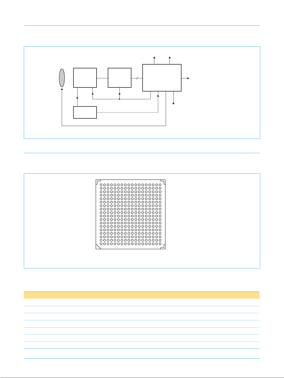
6. Pinning information
6.1 Pinning
handbook, halfpage
V
U
T
R
P
N
M
L
K
J
H
G
F
E
D
C
B
A
to LCD to TV
TDA9952
2 4 6 8 1012141618
1 3 5 7 9 11 13 15 17
10
SAA8122A
to cards
(SSFDC, CF)
USB
IRDA
to PC
FCE687
SAA8122AEL
FCE677
Fig 3. Pin configuration (bottom view).
6.2 Pin description
Table 3: Pin description
Symbol Pin Type Description
V
DDD
V
SSA(DLL)
V
DDA(DLL)
DISP_VSYNC A4 O digital vertical synchronization signal
IO1/IRQ17 A5 I/O I/O port 0 bit 1 or interrupt request 17
V
DDA(LCDG)
V
DDA(OUTPUT2)
9397 750 07048
Objective specification Rev. 01 — 20 April 2000 5 of 26
A1 - digital supply voltage
A2 - analog ground for DLL of PPG
A3 - analog supply voltage for DLL of PPG
A6 P analog supply voltage for DAC component G
A7 P analog supply voltage for DAC video output 2
© Philips Electronics N.V. 2000. All rights reserved.
Page 6

Philips Semiconductors
SAA8122A
Digital Still Camera Processor (ImagIC family)
Table 3: Pin description
…continued
Symbol Pin Type Description
CREF_BG1 A8 - band-gap 1
V
SS(BG)
A9 P ground for BG of video DAC
SYSRSTIN A10 I system reset input/output; active LOW
V
SS(RTC)
A11 P ground for RTC
T0_CAP0 A12 I timer 0 capture input 0
CNT2 A13 I timer 2 count pulse input
CNT1 A14 I timer 1 count pulse input
PWM0 A15 O timer 0 PWM output
ADC0 A16 I analog input signal 0 for level measurement
ADC3 A17 I analog input signal 3 for level measurement
V
SS(ADC)
A18 P ground for ADC
ANPPG1 B1 O PPG analog signal 1
IO6/IRQ22 B4 I/O I/O port 0 bit 6 or interrupt request 22
IO3/IRQ19 B5 I/O I/O port 0 bit 3 or interrupt request 19
LCD_G B6 O analog green signal
VIDEO_OUT2 B7 O video output signal 2
V
SSA(ref)
B8 O analog reference ground
SC_TCK B9 I test clock input for surround scan chains
TCK B10 I test clock input
XTALCCDIN B11 - oscillator input from a specific CCD crystal
V
DDA(SPLL)
V
SS(PLL)
B12 P analog supply voltage for SPLL
B13 P ground for PLL
CNT0 B14 I timer 0 count pulse input
V
SSA(ref)(ADC)
B15 O analog reference ground for ADC
ADC2 B16 I analog input signal 2 for level measurement
V
DDA(ADC)
B17 P analog supply voltage for ADC
IO23 B18 I/O I/O port 2 bit 7
V
DDA(PPG1)
V
DDA(PPG0)
V
DDA(DLL)
C1 P analog supply voltage for PPG
C2 P analog supply voltage for PPG
C3 P analog supply voltage for DLL of PPG
IO7/IRQ23 C4 I/O I/O port 0 bit 7 or interrupt request 23
IO4/IRQ20 C5 I/O I/O port 0 bit 4 or interrupt request 20
LCD_R C6 O analog red signal
LCD_B C7 O analog blue signal
V
DDA(OUTPUT1)
V
DDA(BG)
C8 P analog supply voltage for DAC video output 1
C9 P analog supply voltage for BG of video DAC
TMS C10 I test mode select input
XTAL32KIN C11 - oscillator input from a 32 kHz crystal
XTAL10IN C12 - oscillator input from a 10 MHz crystal
GATE2 C13 I timer 2 gate input
V
DDA(PLL)
C14 P analog supply voltage for PLL
9397 750 07048
Objective specification Rev. 01 — 20 April 2000 6 of 26
© Philips Electronics N.V. 2000. All rights reserved.
Page 7

Philips Semiconductors
SAA8122A
Digital Still Camera Processor (ImagIC family)
Table 3: Pin description
…continued
Symbol Pin Type Description
PWM1 C15 O timer 1 PWM output
ADC1 C16 I analog input signal 1 for level measurement
IO22 C17 I/O I/O port 2 bit 6
IO16 C18 I/O I/O port 2 bit 0
ANPPG7 D1 O PPG analog signal 7
V
SSA(PPG1)
D2 P analog ground for PPG
DISP_HSYNC D3 O digital horizontal synchronization signal
IO5/IRQ21 D4 I/O I/O port 0 bit 5 or interrupt request 21
IO0/IRQ16 D5 I/O I/O port 0 bit 0 or interrupt request 16
V
SSA(LCD)
V
SS(OUTPUT)
D6 P analog ground for display RGB
D7 P ground for DAC video output
CREF_BG2 D8 - band-gap 2
TDO D9 O test data output
TDI D10 I test data input
XTAL32KOUT D11 - oscillator output from a 32 kHz crystal
XTAL10OUT D12 - oscillator output from a 10 MHz crystal
T0_CAP1 D13 I timer 0 capture input 1
GATE0 D14 I timer 0 gate input
PWM2 D15 O timer 2 PWM output
IO17 D16 I/O I/O port 2 bit 1
IO15 D17 I/O I/O port 1 bit 7
IO11 D18 I/O I/O port 1 bit 3
PPG1 E1 O PPG digital signal 0
PPG2 E2 O PPG digital signal 1
ANPPG8 E3 O PPG analog signal 8
V
DDA(PPG0)
E4 P analog supply voltage for PPG
IO2/IRQ18 E5 I/O I/O port 0 bit 2 or interrupt request 18
V
DDA(LCDR)
V
DDA(LCDB)
E6 P analog supply voltage for DAC component R
E7 P analog supply voltage for DAC component B
VIDEO_OUT1 E8 O video output signal 1
SYSRST E9 O system reset output; active LOW
TRST E10 I test reset input
V
DDD(RTC)
E11 P digital supply voltage for RTC
XTALCCDOUT E12 - oscillator output from a specific CCD crystal
GATE1 E14 I timer 1 gate input
IO18 E15 I/O I/O port 2 bit 2
IO10 E16 I/O I/O port 1 bit 2
IO9 E17 I/O I/O port 1 bit 1
UA_CLK E18 I UART external clock
PPG5 F1 O PPG digital signal 4
PPG6 F2 O PPG digital signal 5
9397 750 07048
Objective specification Rev. 01 — 20 April 2000 7 of 26
© Philips Electronics N.V. 2000. All rights reserved.
Page 8

Philips Semiconductors
SAA8122A
Digital Still Camera Processor (ImagIC family)
Table 3: Pin description
…continued
Symbol Pin Type Description
PPG3 F3 O PPG digital signal 2
ANPPG5 F4 O PPG analog signal 5
ANPPG3 F5 O PPG analog signal 3
V
SS
V
SS
V
DD
V
DD
V
DD
V
DD
V
DD
F6 - ground
F7 - ground
F8 - supply voltage
F9 - supply voltage
F10 - supply voltage
F11 - supply voltage
F12 - supply voltage
IO20 F13 I/O I/O port 2 bit 4
IO19 F14 I/O I/O port 2 bit 3
IO12 F15 I/O I/O port 1 bit 4
CTS F16 I UART clear to send
RXD F17 I UART receive input
TXD F18 O UART transmit output
PPG10 G1 O PPG digital signal 17
PPG12 G2 O PPG digital control signal 1
PPG8 G3 O PPG digital signal 8
PPG4 G4 O PPG digital signal 3
ANPPG6 G5 O PPG analog signal 6
ANPPG2 G6 O PPG analog signal 2
V
DD
V
SS
V
SS
V
SS
V
SS
V
DD
G7 - supply voltage
G8 - ground
G9 - ground
G10 - ground
G11 - ground
G12 - supply voltage
IO21 G13 I/O I/O port 2 bit 5
IO13 G14 I/O I/O port 1 bit 5
RTS G15 O UART request to send
2
SDA G16 I/O I
SCL G17 I/O I
C-bus data
2
C-bus clock
n.c. G18 - not connected
HDHREF H1 I/O PPG horizontal synchronization signal
VDVS H2 I/O PPG vertical synchronization signal
PPG13 H3 O PPG digital control signal 2
PPG7 H4 O PPG digital control signal 6
PPG14 H5 O PPG digital control signal 3
ANPPG4 H6 O PPG analog signal 4
V
DD
H7 - supply voltage
9397 750 07048
Objective specification Rev. 01 — 20 April 2000 8 of 26
© Philips Electronics N.V. 2000. All rights reserved.
Page 9

Philips Semiconductors
SAA8122A
Digital Still Camera Processor (ImagIC family)
Table 3: Pin description
…continued
Symbol Pin Type Description
V
SS
V
SS
V
SS
V
SS
V
DD
H8 - ground
H9 - ground
H10 - ground
H11 - ground
H12 - supply voltage
IO14 H13 I/O I/O port 1 bit 6
RXVPI H14 I USB
n.c. H15 - not connected
RXVMI H16 I/O USB
TXVPO H17 O USB
RXDATA H18 I USB
CCD_IM2 J1 I digital image signal 2
CCD_IM3 J2 I digital image signal 3
CCD_IM4 J3 I digital image signal 4
PPG11 J4 O PPG digital signal 18
PPG9 J5 O PPG digital signal 8
V
DD
V
DD
V
SS
V
SS
V
SS
V
SS
V
DD
J6 - supply voltage
J7 - supply voltage
J8 - ground
J9 - ground
J10 - ground
J11 - ground
J12 - supply voltage
IO8 J13 I/O I/O port 1 bit 0
SUSPEND J14 O USB
TXOE J15 O USB
D2 J16 I/O EBIU D2
D3 J17 I/O EBIU D3
D0 J18 I/O EBIU D0
CCD_IM10 K1 I digital image signal 10
CCD_IM9 K2 I digital image signal 9
CCD_IM8 K3 I digital image signal 8
CCD_IM1 K4 I digital image signal 1
CCD_IM0 K5 I digital image signal 0
V
DD
V
DD
V
SS
V
SS
V
SS
V
SS
V
DD
K6 - supply voltage
K7 - supply voltage
K8 - ground
K9 - ground
K10 - ground
K11 - ground
K12 - supply voltage
9397 750 07048
Objective specification Rev. 01 — 20 April 2000 9 of 26
© Philips Electronics N.V. 2000. All rights reserved.
Page 10

Philips Semiconductors
SAA8122A
Digital Still Camera Processor (ImagIC family)
Table 3: Pin description
…continued
Symbol Pin Type Description
TXVMO K13 O USB
D1 K14 I/O EBIU D1
D4 K15 I/O EBIU D4
D6 K16 I/O EBIU D6
D7 K17 I/O EBIU D7
D8 K18 I/O EBIU D8
SD_A[0] L1 O SDRAM controller address bus bit 0
SD_A[3] L2 O SDRAM controller address bus bit 3
SD_A[2] L3 O SDRAM controller address bus bit 2
CCD_IM6 L4 I digital image signal 6
CCD_IM7 L5 I digital image signal 7
CCD_IM5 L6 I digital image signal 5
V
DD
V
SS
V
SS
V
SS
V
SS
V
DD
L7 - supply voltage
L8 - ground
L9 - ground
L10 - ground
L11 - ground
L12 - supply voltage
D5 L13 I/O EBIU D5
D9 L14 I/O EBIU D9
D11 L15 I/O EBIU D11
D14 L16 I/O EBIU D14
D13 L17 I/O EBIU D13
D12 L18 I/O EBIU D12
SD_A[7] M1 O SDRAM controller address bus bit 7
SD_A[8] M2 O SDRAM controller address bus bit 8
SD_A[9] M3 O SDRAM controller address bus bit 9
SD_A[4] M4 O SDRAM controller address bus bit 4
SD_A[1] M5 O SDRAM controller address bus bit 1
CCD_IM11 M6 I digital image signal 11
V
DD
V
SS
V
SS
V
SS
V
SS
V
DD
M7 - supply voltage
M8 - ground
M9 - ground
M10 - ground
M11 - ground
M12 - supply voltage
D10 M13 I/O EBIU D10
SC_SE M14 O EBIU controller SE signal for SSFDC card; active LOW
D15 M15 I/O EBIU D15
PC_WAIT2 M16 I EBIU controller WAIT signal for PC card 2; active LOW
SC_CE M17 O EBIU controller CE signal for SSFDC card; active LOW
9397 750 07048
Objective specification Rev. 01 — 20 April 2000 10 of 26
© Philips Electronics N.V. 2000. All rights reserved.
Page 11

Philips Semiconductors
SAA8122A
Digital Still Camera Processor (ImagIC family)
Table 3: Pin description
…continued
Symbol Pin Type Description
SC_CLE M18 O EBIU controller CLE signal for SSFDC card
SD_A[12] N1 O SDRAM controller address bus bit 12
SD_A[13] N2 O SDRAM controller address bus bit 13
SD_A[14] N3 O SDRAM controller address bus bit 14
SD_A[10] N4 O SDRAM controller address bus bit 10
SD_A[6] N5 O SDRAM controller address bus bit 6
SD_A[5] N6 O SDRAM controller address bus bit 5
V
DD
V
DD
V
DD
V
DD
V
DD
N7 - supply voltage
N8 - supply voltage
N9 - supply voltage
N10 - supply voltage
N11 - supply voltage
SC_ALE N12 O EBIU controller ALE signal for SSFDC card
PC2_CE1 N13 O EBIU controller CE1 signal for PC card 2; active LOW
PC2_CE2 N14 O EBIU controller CE2 signal for PC card 2; active LOW
PC_REG N15 O EBIU controller REG signal for PC cards; active LOW
PC_WAIT1 N16 O EBIU controller WAIT signal for PC card 1; active LOW
IOWR_WE N17 O EBIU controller IORD signal for PC cards; active LOW
IORD_RE N18 O EBIU controller IORD signal for PC cards; active LOW
SD_CLKOUT P1 O SDRAM controller clock output
SD_CLKIN P2 I SDRAM controller clock input
SD_CS2 P3 O SDRAM controller chip select for memory 2; active LOW
SD_CLKEN P4 O SDRAM controller clock enable
SD_A[11] P5 O SDRAM controller address bus bit 11
V
DD
P6 - supply voltage
SD_D[7] P7 I/O SDRAM controller data bus bit 7
IO25 P8 I/O I/O port 3 bit 1
IO38 P9 I/O I/O port 4 bit 6
A25 P10 I/O EBIU A25 (Strapin[0] during boot sequence)
A21 P11 I/O EBIU A21 (Strapin[4] during boot sequence)
V
DD
P12 - supply voltage
A14 P13 I/O EBIU A14
SCLK P14 O EBIU controller clock signal for external peripherals
A9 P15 I/O EBIU A9
CAS0 P16 O EBIU controller CAS signal for DRAM memory for lower byte; used as data
strobe signal for lower byte for general chip select; active LOW
PC1_CE1 P17 O EBIU controller CE1 signal for PC card 1; active LOW
PC1_CE2 P18 O EBIU controller CE2 signal for PC card 1; active LOW
SD_CS0 R1 O SDRAM controller chip select for memory 0; active LOW
SD_CS1 R2 O SDRAM controller chip select for memory 1; active LOW
SD_CS3 R3 O SDRAM controller chip select for memory 3; active LOW
9397 750 07048
Objective specification Rev. 01 — 20 April 2000 11 of 26
© Philips Electronics N.V. 2000. All rights reserved.
Page 12

Philips Semiconductors
SAA8122A
Digital Still Camera Processor (ImagIC family)
Table 3: Pin description
Symbol Pin Type Description
SD_D[4] R4 I/O SDRAM controller data bus bit 4
SD_RAS R5 O SDRAM controller row address strobe; active LOW
SD_D[6] R6 I/O SDRAM controller data bus bit 6
SD_D[13] R7 I/O SDRAM controller data bus bit 13
IO30 R8 I/O I/O port 3 bit 6
IO37 R9 I/O I/O port 4 bit 5
A24 R10 I/O EBIU A24 (Strapin[1] during boot sequence)
A19 R11 I/O EBIU A19 (Strapin[6] and Strapin[9] during boot sequence)
A18 R12 I/O EBIU A18 (Strapin[10] during boot sequence)
A13 R13 I/O EBIU A13
A5 R14 O EBIU A5
CS6 R15 O EBIU controller chip select 6; active LOW
CAS1 R16 O EBIU controller CAS signal for DRAM memory for upper byte; used as data
OE R17 O EBIU controller output enable signal; active LOW
RAS R18 O EBIU controller RAS signal for DRAM memory; active LOW
SD_CAS T1 O SDRAM controller column address strobe; active LOW
SD_WE T2 O SDRAM controller write enable; active LOW
SD_D[3] T3 I/O SDRAM controller data bus bit 3
SD_D[8] T4 I/O SDRAM controller data bus bit 8
SD_D[10] T5 I/O SDRAM controller data bus bit 10
SD_D[14] T6 I/O SDRAM controller data bus bit 14
IO26 T7 I/O I/O port 3 bit 2
IO29 T8 I/O I/O port 3 bit 5
IO33 T9 I/O I/O port 4 bit 1
IO36 T10 I/O I/O port 4 bit 4
A23 T11 I/O EBIU A23 (Strapin[2] during boot sequence)
A16 T12 I/O EBIU A16
A12 T13 I/O EBIU A12
A3 T14 O EBIU A3
CS7 T15 O EBIU controller chip select 7; active LOW
CS4 T16 O EBIU controller chip select 4; active LOW
WE T17 O EBIU controller write enable signal; active LOW
CS_WAIT T18 O EBIU controller wait signal for chip selects; active LOW
SD_DQM0 U1 O SDRAM controller DQ mask enable for byte 0; active LOW
SD_DQM1 U2 O SDRAM controller DQ mask enable for byte 1; active LOW
SD_D[2] U3 I/O SDRAM controller data bus bit 2
SD_D[9] U4 I/O SDRAM controller data bus bit 9
SD_D[11] U5 I/O SDRAM controller data bus bit 11
SD_D[15] U6 I/O SDRAM controller data bus bit 15
IO27 U7 I/O I/O port 3 bit 3
…continued
strobe signal for upper byte for general chip select; active LOW
9397 750 07048
Objective specification Rev. 01 — 20 April 2000 12 of 26
© Philips Electronics N.V. 2000. All rights reserved.
Page 13

Philips Semiconductors
SAA8122A
Digital Still Camera Processor (ImagIC family)
Table 3: Pin description
Symbol Pin Type Description
IO32 U8 I/O I/O port 4 bit 0
IO34 U9 I/O I/O port 4 bit 2
A22 U10 I/O EBIU A22 (Strapin[3] during boot sequence)
A17 U11 I/O EBIU A17 (Strapin[11] during boot sequence)
A11 U12 I/O EBIU A11
A8 U13 I/O EBIU A8
A4 U14 O EBIU A4
A2 U15 O EBIU A2
CS5 U16 O EBIU controller chip select 5; active LOW
CS3 U17 O EBIU controller chip select 3; active LOW
CS0 U18 O EBIU controller chip select 0; active LOW
SD_D[0] V1 I/O SDRAM controller data bus bit 0
SD_D[1] V2 I/O SDRAM controller data bus bit 1
SD_D[5] V3 I/O SDRAM controller data bus bit 5
SD_D[12] V4 I/O SDRAM controller data bus bit 12
IO24 V5 I/O I/O port 3 bit 0
IO28 V6 I/O I/O port 3 bit 4
IO31 V7 I/O I/O port 3 bit 7
IO35 V8 I/O I/O port 4 bit 3
IO39 V9 I/O I/O port 4 bit 7
A20 V10 I/O EBIU A20 (Strapin[5] and Strapin[8] during boot sequence)
A15 V11 I/O EBIU A15
A10 V12 I/O EBIU A10
A7 V13 I/O EBIU A7
A6 V14 I/O EBIU A6
A1 V15 O EBIU A1
A0 V16 O EBIU A0
CS2 V17 O EBIU controller chip select 2; active LOW
CS1 V18 O EBIU controller chip select 1; active LOW
…continued
9397 750 07048
Objective specification Rev. 01 — 20 April 2000 13 of 26
© Philips Electronics N.V. 2000. All rights reserved.
Page 14

Philips Semiconductors
7. Limiting values
Table 4: Limiting values
In accordance with the Absolute Maximum Rating System (IEC 60134).
Symbol Parameter Conditions Min Max Unit
V
V
V
I
DD
I
SS
T
[1] Value may not exceed 4 V.
[2] Including voltage on outputs in 3-state mode.
[3] Only valid when supply voltage is present.
[4] The peak current is limited to 10 times the corresponding maximum current.
[5] Dependent of package and not yet determined.
DDD
DDA
I
stg
SAA8122A
Digital Still Camera Processor (ImagIC family)
digital supply voltage −0.5 4 V
analog supply voltage −0.5 4 V
DC input voltage general
5 V tolerant
cells only
DC supply current per
supply pin
DC ground current per
ground pin
storage temperature
[1]
−0.5 VDD+ 0.5 V
[2]
[2]
−0.5 −0.5 V
[3]
[4]
− 60 mA
[4]
− 60 mA
[5]
0 125 °C
8. Characteristics
Table 5: General supply characteristics
Symbol Parameter Conditions Min Typ Max Unit
V
DDD
V
DDA(DLL)
V
DDA(LCDR)
V
DDA(LCDG)
V
DDA(LCDB)
V
DDA(OUTPUT1)
V
DDA(OUTPUT2)
V
DDA(ADC)
V
DDA(PPG1)
V
DDA(PPG0)
V
DDA(BG)
V
DDA(PLL)
V
DDA(SPLL)
V
DDD(RTC)
[1] V
DDD(RTC)
digital supply voltage 3.0 3.3 3.6 V
analog supply voltage for DLL 3.0 3.3 3.6 V
analog supply voltage for LCDR output of DAC 3.0 3.3 3.6 V
analog supply voltage for LCDG output of DAC 3.0 3.3 3.6 V
analog supply voltage for LCDB 3.0 3.3 3.6 V
analog supply voltage for video output 1 of DAC 3.0 3.3 3.6 V
analog supply voltage for video output 2 of DAC 3.0 3.3 3.6 V
analog supply voltage for ADC 3.0 3.3 3.6 V
analog supply voltage for PPG 3.0 3.3 3.6 V
analog supply voltage for PPG 3.0 3.3 3.6 V
analog supply voltage for bandgap 3.0 3.3 3.6 V
analog supply voltage for PLL 3.0 3.3 3.6 V
analog supply voltage for SPLL 3.0 3.3 3.6 V
digital supply voltage for RTC
is the single supply which may be on when the others are off. In this case the I/Os of the SAA8122A have to be at 0 V.
[1]
3.0 3.3 3.6 V
9397 750 07048
Objective specification Rev. 01 — 20 April 2000 14 of 26
© Philips Electronics N.V. 2000. All rights reserved.
Page 15

Philips Semiconductors
SAA8122A
Digital Still Camera Processor (ImagIC family)
Table 6: Operating characteristics
Symbol Parameter Conditions Min Typ Max Unit
V
DDA(LCDR)
analog supply voltage for LCDR
output of DAC
V
DDA(LCDG)
analog supply voltage for LCDG
output of DAC
V
DDA(LCDB)
analog supply voltage for LCDB
output of DAC
V
DDA(OUTPUT1)
analog supply voltage for video
output 1 of DAC
V
DDA(OUTPUT2)
analog supply voltage for video
output 2 of DAC
V
DDA(BG)
V
BG
V
OL
V
OH
analog supply voltage for bandgap 3.0 3.3 3.6 V
bandgap reference voltage (4σ) 1.18 1.22 1.26 V
LOW-level output voltage code 0 - 0.225 - V
HIGH-level output voltage code 511 - 1.625 - V
LCD channels (1 kΩ buffer)
R
L
C
L
load resistance - 1 - kΩ
load capacitance - - 5 pF
RES resolution - 8 - bit
LCD channels (75 Ω mode)
R
L
C
L
load resistance - 75 - Ω
load capacitance - 5 100 pF
RES resolution - 9 - bit
VIDEO_OUT channels (1 kΩ buffer)
R
L
C
L
load resistance - 1 - kΩ
load capacitance - - 5 pF
RES resolution - 8 - bit
VIDEO_OUT channels (1 kΩ mode)
R
L
C
L
load resistance - 1 - kΩ
load capacitance - - 5 pF
RES resolution - 9 - bit
ADC
V
DDA(ADC)
analog supply voltage for analog
ADC
∆V
DD
supply voltage difference between
and V
V
DDA
DDA(ADC)
RES resolution 8 - 10 bit
C
i
V
i
f
sample
input capacitance - 2 - pF
input voltage 0 - 3.3 V
sample frequency 8-bit 0 - 100 kHz
PLL
V
DDA(PLL)
analog supply voltage for analog
PLL
3.0 3.3 3.6 V
3.0 3.3 3.6 V
3.0 3.3 3.6 V
3.0 3.3 3.6 V
3.0 3.3 3.6 V
3.0 3.3 3.6 V
- - 0.2 V
3.0 3.3 3.6 V
9397 750 07048
Objective specification Rev. 01 — 20 April 2000 15 of 26
© Philips Electronics N.V. 2000. All rights reserved.
Page 16

Philips Semiconductors
SAA8122A
Digital Still Camera Processor (ImagIC family)
Table 6: Operating characteristics
…continued
Symbol Parameter Conditions Min Typ Max Unit
∆V
f
clk
DD
supply voltage difference between
and V
V
DDA
DDA(PLL)
- - 0.2 V
clock frequency - 96 - MHz
SPLL
V
DDA(SPLL)
analog supply voltage for analog
3.0 3.3 3.6 V
SPLL
∆V
DD
supply voltage difference between
and V
V
DDA
DDA(SPLL)
- - 0.2 V
Power-on reset
V
trip
t
HIGH
trip level of power-on reset 1.5 2.07 2.65 V
time that V
has to be above
DDA
--2µs
2.65 V beforeinternalreset signal is
asserted
t
LOW
time that V
has to be above
DDA
--8µs
2.65 V beforeinternalreset signal is
de-asserted
Analog PPG
V
DDA(DLL)
analog supply voltage for analog
3.0 3.3 3.6 V
DLL
∆V
DD-DDA(DLL)
V
DDA(PPG1)
V
DDA(PPG0)
∆V
DD-DDA(PPG)
I/Os (V
DDD=VDDA, Tamb
supply voltage difference between
and V
V
DDA
;
analog supply voltage for analog
DDA(DLL)
PPG
supply voltage difference between
V
DDA
and V
DDA(PPG1)
or V
= 0 to 60 °C)
- - 0.2 V
3.0 3.3 3.6 V
- - 0.2 V
DDA(PPG0)
Data and control inputs
SD_CLKIN
V
IL
V
IH
C
i
I
IL
I
IH
I
lu(I/O)
LOW-level digital input voltage 0 - 0.3V
HIGH-level digital input voltage 0.7V
DDD
-V
DDD
DDD
V
V
input capacitance - 1.14 - pF
LOW-level input current VI=0V --1µA
HIGH-level input current VI=V
DDD
I/O latch-up current −0.5<V
+ 0.5 100 - - mA
DDD
--1µA
CS_WAIT, PC_WAIT1, PC_WAIT2, SC_TCK, TCK, TDI, TMS, TRST, CCD_IM0 to CCD_IM11, CNT0 to CNT2,
GATE0 to GATE2, T0_CAP0, T0_CAP1, CTS, RXD, UA_CLK, RXDATA, RXVMI, RXVPI
V
IL
V
IH
C
i
I
IL
I
IH
I
lu(I/O)
LOW-level digital input voltage 0 - 0.8 V
HIGH-level digital input voltage 2.0 - 5.5 V
input capacitance - 1.2 - pF
LOW-level input current VI=0V --1µA
HIGH-level input current VI=V
DDD
I/O latch-up current −0.5<V
< 5.5 100 - - mA
DDD
--1µA
SYSRSTIN
V
IL
LOW-level digital input voltage 0 - 0.8 V
9397 750 07048
Objective specification Rev. 01 — 20 April 2000 16 of 26
© Philips Electronics N.V. 2000. All rights reserved.
Page 17

Philips Semiconductors
SAA8122A
Digital Still Camera Processor (ImagIC family)
Table 6: Operating characteristics
…continued
Symbol Parameter Conditions Min Typ Max Unit
V
IH
V
hys
C
i
I
IL
I
IH
I
lu(I/O)
HIGH-level digital input voltage 2.0 - 5.5 V
hysteresis voltage 0.4 - - V
input capacitance - 1.2 - pF
LOW-level input current VI=0V --1µA
HIGH-level input current VI=V
DDD
I/O latch-up current −0.5<V
< 5.5 100 - - mA
DDD
--1µA
Data and control outputs
ANPPG1 to ANPPG8
V
OL
V
OH
C
o(L)(max)
I
OL
I
OH
LOW-level digital output voltage IOL= 4 mA 0 - 0.4 V
HIGH-level digital output voltage IOH= 4 mA V
maximum output load capacitance
[1]
LOW-level output current VOL= 0.4 V;
V
OH=VDDA
HIGH-level output current VOH=V
− 0.4
− 0.4 −4--mA
DDA
− 0.4 - V
DDA
DDA
- - 100 pF
4--mA
V
SCLK, SD_A[0] to SD_A[14], SD_CAS, SD_CLKEN, SD_CLKOUT, SD_CS0 to SD_CS3, SD_DQM0 to SD_DQM1,
SD_RAS, SD_WE
V
OL
V
OH
C
i
C
o(L)(max)
I
OL
I
OH
I
OZ
LOW-level digital output voltage IOL= 4 mA 0 - 0.4 V
HIGH-level digital output voltage IOH= −4mA V
− 0.4 V
DDD
DDD
V
input capacitance - - 1 - pF
maximum output load capacitance -
[1]
- - 100 pF
LOW-level output current VOL= 0.4 V - - - µA
HIGH-level output current VOH=V
3-state output leakage current VO=0;
V
O=VDDD
− 0.4 −4--mA
DDD
--1µA
TDO, SYSRST, PWM0 to PWM2, RTS, TXD, SUSPEND, TXOE, TXVMO, TXVPO, DISP_HSYNC, DISP_VSYNC
V
OL
V
OH
C
i
C
o(L)(max)
I
OL
I
OH
I
OZ
LOW-level digital output voltage IOL= 2 mA 0 - 0.4 V
HIGH-level digital output voltage IOH= −2mA V
− 0.4 - V
DDD
DDD
V
input capacitance - - 2.2 - pF
maximum output load capacitance LOW-level output current VOL= 0.4 V;
V
OH=VDDD
HIGH-level output current VOH=V
DDD
3-state output leakage current VO=0;
V
O=VDD
− 0.4
− 0.4 −2--mA
[1]
--30pF
2--mA
--1µA
CAS0, CAS1, CS0 to CS7, IORD_RE, IOWR_WE, OE, PC_REG, PC1_CE1, PC1_CE2, RAS, SC_ALE, SC_SE, WE,
PPG1 to PPG14
V
OL
V
OH
C
i
C
o(L)(max)
I
OL
I
OH
LOW-level digital output voltage IOL= 4 mA 0 - 0.4 V
HIGH-level digital output voltage IOH= −4mA V
− 0.4 - V
DDD
DDD
V
input capacitance - - 2.4 - pF
maximum output load capacitance LOW-level output current VOL= 0.4 V;
V
OH=VDDD
HIGH-level output current VOH=V
DDD
− 0.4
− 0.4 −4--mA
[1]
--30pF
4--mA
9397 750 07048
Objective specification Rev. 01 — 20 April 2000 17 of 26
© Philips Electronics N.V. 2000. All rights reserved.
Page 18

Philips Semiconductors
SAA8122A
Digital Still Camera Processor (ImagIC family)
Table 6: Operating characteristics
…continued
Symbol Parameter Conditions Min Typ Max Unit
I
OZ
3-state output leakage current VO=0;
V
O=VDDD
--1µA
Data and control I/Os
SD_D[0] to SD_D[15]
V
IL
V
IH
V
OL
V
OH
C
i
C
o(L)(max)
I
OL
I
OH
I
OZ
I
IL
I
IH
LOW-level digital input voltage - 0 - 0.3V
HIGH-level digital input voltage - 0.7V
DDD
-V
DDD
DDD
V
V
LOW-level digital output voltage IOL= 4 mA 0 - 0.4 V
HIGH-level digital output voltage IOH= −4mA V
− 0.4 - V
DDD
DDD
V
input capacitance - - 1.2 - pF
maximum output load capacitance LOW-level output current VOL= 0.4 V;
V
OH=VDDD
HIGH-level output current VOH=V
DDD
3-state output leakage current VO=0;
V
O=VDDD
− 0.4
− 0.4 −4--mA
[1]
- - 100 pF
4--mA
--1µA
LOW-level input current VI=0 --1µA
HIGH-level input current VI=V
DDD
--1µA
A0 to A15, IO8 to IO15, HDHREF, VDVS
V
IL
V
IH
V
OL
V
OH
C
i
C
o(L)(max)
I
OL
I
OH
I
OZ
I
IL
I
IH
LOW-level digital input voltage - 0 - 0.6V
HIGH-level digital input voltage - 0.7V
DDD
-V
DDD
DDD
V
V
LOW-level digital output voltage IOL= 4 mA 0 - 0.4 V
HIGH-level digital output voltage IOH= −4mA V
− 0.4 - V
DDD
DDD
V
input capacitance - - 2.5 - pF
maximum output load capacitance LOW-level output current VOL= 0.4 V;
V
OH=VDDD
HIGH-level output current VOH=V
DDD
3-state output leakage current VO=0;
V
O=VDDD
− 0.4
− 0.4 −4--mA
[1]
--30pF
4--mA
--1µA
LOW-level input current VI=0 --1µA
HIGH-level input current VI=V
DDD
--1µA
IO16 to IO23, IO0/IRQ16, IO1/IRQ17, IO2/IRQ18, IO3/IRQ19, IO4/IRQ20, IO5/IRQ21, IO6/IRQ22, IO7/IRQ23
V
IL
V
IH
V
OL
V
OH
C
i
C
o(L)(max)
I
OL
I
OH
LOW-level digital input voltage - 0 - 0.3V
HIGH-level digital input voltage - 0.7V
DDD
-V
DDD
DDD
V
V
LOW-level digital output voltage IOL= 2 mA 0 - 0.4 V
HIGH-level digital output voltage IOH= −2mA V
− 0.4 - - V
DDD
input capacitance - - 2.3 - pF
maximum output load capacitance - - - 30 pF
LOW-level output current VOL= 0.4 V;
V
OH=VDDD
HIGH-level output current VOH=V
DDD
− 0.4
− 0.4 −2--mA
2--mA
9397 750 07048
Objective specification Rev. 01 — 20 April 2000 18 of 26
© Philips Electronics N.V. 2000. All rights reserved.
Page 19

Philips Semiconductors
SAA8122A
Digital Still Camera Processor (ImagIC family)
Table 6: Operating characteristics
…continued
Symbol Parameter Conditions Min Typ Max Unit
I
OZ
I
IL
I
IH
3-state output leakage current VO=0;
V
O=VDDD
--1µA
LOW-level input current VI=0 --1µA
HIGH-level input current VI=V
DDD
--1µA
IO4 to IO31
V
IL
V
IH
V
OL
V
OH
C
i
C
o(L)(max)
I
OL
I
OH
I
OZ
I
IL
I
IH
LOW-level digital input voltage - 0 - 0.8 V
HIGH-level digital input voltage - 2.0 - 5.5 V
LOW-level digital output voltage IOL= 2 mA - - 0.4 V
HIGH-level digital output voltage IOH= −2mA V
− 0.4 - V
DDD
DDD
V
input capacitance - - 1.5 - pF
maximum output load capacitance - - - 30 pF
LOW-level output current VOL= 0.4 V;
V
OH=VDDD
HIGH-level output current VOH=V
DDD
3-state output leakage current VO=0;
V
O=VDDD
− 0.4
− 0.4 −2--mA
2--mA
--1µA
LOW-level input current VI=0 --1µA
HIGH-level input current VI=V
DDD
--1µA
IO32 to IO39
V
IL
V
IH
V
OL
V
OH
C
i
C
o(L)(max)
I
OL
I
OH
I
OZ
I
IL
I
IH
2
C-bus I/Os
I
LOW-level digital input voltage - 0 - 0.8 V
HIGH-level digital input voltage - 2.0 - 5.5 V
LOW-level digital output voltage IOL= 1 mA 0 - 0.4 V
HIGH-level digital output voltage IOH= −1mA V
− 0.4 - V
DDD
DDD
V
input capacitance - - 1.4 - pF
maximum output load capacitance - - - 30 pF
LOW-level output current VOL= 0.4 V;
V
OH=VDDD
HIGH-level output current VOH=V
DDD
3-state output leakage current VO=0;
V
O=VDDD
− 0.4
− 0.4 −1--mA
1--mA
--1µA
LOW-level input current VI=0 --1µA
HIGH-level input current VI=V
DDD
--1µA
SCL and SDA
V
IL
V
IH
V
hys
V
OL
C
i
C
o(L)(max)
LOW-level digital input voltage - 0 - 0.3V
HIGH-level digital input voltage - 0 - 0.3V
hysteresis voltage - 0.005V
--V
DDD
DDD
DDD
V
V
LOW-level digital output voltage IOL= 3 mA - - 0.4 V
input capacitance - - 3.2 - pF
maximum output load capacitance -
[1]
- - 400 pF
9397 750 07048
Objective specification Rev. 01 — 20 April 2000 19 of 26
© Philips Electronics N.V. 2000. All rights reserved.
Page 20

Philips Semiconductors
SAA8122A
Digital Still Camera Processor (ImagIC family)
Table 6: Operating characteristics
…continued
Symbol Parameter Conditions Min Typ Max Unit
I
OZ
I
IL
I
IH
[1] The maximum capacitance value given does not take into account the signal frequency. For critical signals the maximum capacitance
has to be weighted according to the signal frequency and external devices constraints.
3-state output leakage VO=0;
V
O=VDDD
--1µA
LOW-level input current VI=0 --1µA
HIGH-level input current VI=V
DDD
--1µA
9397 750 07048
Objective specification Rev. 01 — 20 April 2000 20 of 26
© Philips Electronics N.V. 2000. All rights reserved.
Page 21

Philips Semiconductors
9. Package outline
SAA8122A
Digital Still Camera Processor (ImagIC family)
LFBGA324: plastic low profile fine-pitch ball grid array package; 324 balls; body 16 x 16 x 1.2 mm
A
B
E
M
vB
vA
e
E
1
A
2
A
A
1
detail X
C
y
C
M
1
y
X
ball A1
index area
D
D
1
e
V
U
T
R
P
N
M
L
K
J
H
G
F
E
D
C
B
A
2 4 6 8 1012141618
1 3 5 7 9 11 13 15 17
b
∅ w
M
SOT571-1
5 10 mm
scale
0.8
0.15v0.1
w
ye
y
0.12 0.10
1
EUROPEAN
PROJECTION
ISSUE DATE
00-01-20
DIMENSIONS (mm are the original dimensions)
A
UNIT
mm
OUTLINE
VERSION
SOT571-1 MO-205
max.
1.70
A
1bA2
0.45
0.35
D
D
1.35
1.05
16.1
0.55
15.9
0.45
IEC JEDEC EIAJ
1
16.1
15.9
0
E
E
1
13.613.6
REFERENCES
Fig 4. SOT571-1.
9397 750 07048
Objective specification Rev. 01 — 20 April 2000 21 of 26
© Philips Electronics N.V. 2000. All rights reserved.
Page 22

Philips Semiconductors
10. Soldering
10.1 Introduction to soldering surface mount packages
This text gives a very brief insight to a complex technology. A more in-depth account
of soldering ICs can be found in our
Packages
There is no soldering method that is ideal for all surface mount IC packages. Wave
soldering is not always suitable for surface mount ICs, or for printed-circuit boards
with high population densities. In these situations reflow soldering is often used.
10.2 Reflow soldering
Reflow soldering requires solder paste (a suspension of fine solder particles, flux and
binding agent) to be applied to the printed-circuit board by screen printing, stencilling
or pressure-syringe dispensing before package placement.
Several methods exist for reflowing; for example, infrared/convection heating in a
conveyor type oven. Throughput times (preheating, soldering and cooling) vary
between 100 and 200 seconds depending on heating method.
SAA8122A
Digital Still Camera Processor (ImagIC family)
Data Handbook IC26; Integrated Circuit
(document order number 9398 652 90011).
Typical reflow peak temperatures range from 215 to 250 °C. The top-surface
temperature of the packages should preferable be kept below 230 °C.
10.3 Wave soldering
Conventional single wave soldering is not recommended for surface mount devices
(SMDs) or printed-circuit boards with a high component density, as solder bridging
and non-wetting can present major problems.
To overcome these problems the double-wave soldering method was specifically
developed.
If wave soldering is used the following conditions must be observed for optimal
results:
Use a double-wave soldering method comprising a turbulent wave with high
•
upward pressure followed by a smooth laminar wave.
For packages with leads on two sides and a pitch (e):
•
– larger than or equal to 1.27 mm, the footprint longitudinal axis is preferred to be
parallel to the transport direction of the printed-circuit board;
– smaller than 1.27 mm, the footprint longitudinal axis must be parallel to the
transport direction of the printed-circuit board.
The footprint must incorporate solder thieves at the downstream end.
For packages with leads on four sides, the footprint must be placed at a 45° angle
•
to the transport direction of the printed-circuit board. The footprint must
incorporate solder thieves downstream and at the side corners.
9397 750 07048
Objective specification Rev. 01 — 20 April 2000 22 of 26
© Philips Electronics N.V. 2000. All rights reserved.
Page 23

Philips Semiconductors
During placement and before soldering, the package must be fixed with a droplet of
adhesive. The adhesive can be applied by screen printing, pin transfer or syringe
dispensing. The package can be soldered after the adhesive is cured.
Typical dwell time is 4 seconds at 250 °C. A mildly-activated flux will eliminate the
need for removal of corrosive residues in most applications.
10.4 Manual soldering
Fix the component by first soldering two diagonally-opposite end leads. Use a low
voltage (24 V or less) soldering iron applied to the flat part of the lead. Contact time
must be limited to 10 seconds at up to 300 °C.
When using a dedicated tool, all other leads can be soldered in one operation within
2 to 5 seconds between 270 and 320 °C.
10.5 Package related soldering information
Table 7: Suitability of surface mount IC packages for wave and reflow soldering
Package Soldering method
BGA, LFBGA, SQFP, TFBGA not suitable suitable
HBCC, HLQFP, HSQFP, HSOP, HTQFP,
HTSSOP, SMS
PLCC
LQFP, QFP, TQFP not recommended
SSOP, TSSOP, VSO not recommended
SAA8122A
Digital Still Camera Processor (ImagIC family)
methods
Wave Reflow
not suitable
[3]
, SO, SOJ suitable suitable
[2]
[3][4]
[5]
suitable
suitable
suitable
[1]
[1] All surface mount (SMD) packages are moisture sensitive. Depending upon the moisture content, the
maximum temperature (with respect to time) and body size of the package, there is a risk that internal
or external package cracks may occur due to vaporization of the moisture in them (the so called
popcorn effect). For details, refer to the Drypack information in the
Circuit Packages; Section: Packing Methods
[2] These packages are not suitable for wavesoldering as a solder joint between the printed-circuit board
and heatsink (at bottom version) can not be achieved,and as solder may stick to the heatsink (on top
version).
[3] If wave soldering is considered, then the package must be placed at a 45° angle to the solder wave
direction. The package footprint must incorporate solder thieves downstream and at the side corners.
[4] Wave soldering is only suitable for LQFP, QFP and TQFP packages with a pitch (e) equal to or larger
than 0.8 mm; it is definitely not suitable for packages with a pitch (e) equal to or smaller than 0.65 mm.
[5] Wave soldering is only suitable for SSOP and TSSOP packages with a pitch (e) equal to or larger than
0.65 mm; it is definitely not suitable for packages with a pitch (e) equal to or smaller than 0.5 mm.
.
Data Handbook IC26; Integrated
11. Revision history
Table 8: Revision history
Rev Date CPCN Description
01 20000420 - Objective specification; initial version
9397 750 07048
Objective specification Rev. 01 — 20 April 2000 23 of 26
© Philips Electronics N.V. 2000. All rights reserved.
Page 24

Philips Semiconductors
12. Data sheet status
SAA8122A
Digital Still Camera Processor (ImagIC family)
Datasheet status Product status Definition
Objective specification Development This data sheet contains the design target or goal specifications for product development. Specification may
change in any manner without notice.
Preliminary specification Qualification This data sheet contains preliminary data, and supplementary data will be published at a later date. Philips
Semiconductors reserves the right to make changes at any time without notice in order to improve design and
supply the best possible product.
Product specification Production This data sheet contains final specifications. Philips Semiconductors reserves the right to make changes at any
time without notice in order to improve design and supply the best possible product.
[1] Please consult the most recently issued data sheet before initiating or completing a design.
13. Definitions
Short-form specification — The data in a short-form specification is
extracted from a full data sheet with the same type number and title. For
detailed information see the relevant data sheet or data handbook.
Limiting values definition — Limiting values given are in accordance with
the Absolute Maximum Rating System (IEC 60134). Stress above one or
more of the limiting values may cause permanent damage to the device.
These are stress ratings only and operation of the device at these or at any
other conditions above those given in the Characteristics sections of the
specification is not implied. Exposure to limiting values for extended periods
may affect device reliability.
Application information — Applications that are described herein for any
of these products are for illustrative purposes only. Philips Semiconductors
make no representation or warranty that such applications will be suitable for
the specified use without further testing or modification.
14. Disclaimers
Life support — These products are not designed for use in life support
appliances, devices, or systems where malfunction of these products can
reasonably be expected to result in personal injury. Philips Semiconductors
[1]
customers using or selling these products for use in such applications do so
at their own risk and agree to fully indemnify Philips Semiconductors for any
damages resulting from such application.
Right to make changes — Philips Semiconductors reserves the right to
make changes, without notice, in the products, including circuits, standard
cells, and/or software, described or contained herein in order to improve
design and/or performance. Philips Semiconductors assumes no
responsibility or liability for the use of any of these products, conveys no
licence or title under any patent, copyright, or mask work right to these
products, and makes no representations or warranties that these products
are free from patent, copyright, or mask work right infringement, unless
otherwise specified.
15. Licenses
Purchase of Philips I2C components
2
Purchase of Philips I
under the Philips’ I
2
I
C system provided the system conforms to the I2C
specification defined by Philips. This specification can be
ordered using the code 9398 393 40011.
C components conveys a license
2
C patent to use the components in the
9397 750 07048
© Philips Electronics N.V. 2000 All rights reserved.
Objective specification Rev. 01 — 20 April 2000 24 of 26
Page 25

Philips Semiconductors
SAA8122A
Digital Still Camera Processor (ImagIC family)
Philips Semiconductors - a worldwide company
Argentina: see South America
Australia: Tel. +61 2 9704 8141, Fax. +61 2 9704 8139
Austria: Tel. +43 160 101, Fax. +43 160 101 1210
Belarus: Tel. +375 17 220 0733, Fax. +375 17 220 0773
Belgium: see The Netherlands
Brazil: see South America
Bulgaria: Tel. +359 268 9211, Fax. +359 268 9102
Canada: Tel. +1 800 234 7381
China/Hong Kong: Tel. +852 2 319 7888, Fax. +852 2 319 7700
Colombia: see South America
Czech Republic: see Austria
Denmark: Tel. +45 3 288 2636, Fax. +45 3 157 0044
Finland: Tel. +358 961 5800, Fax. +358 96 158 0920
France: Tel. +33 14 099 6161, Fax. +33 14 099 6427
Germany: Tel. +49 40 23 5360, Fax. +49 402 353 6300
Hungary: see Austria
India: Tel. +91 22 493 8541, Fax. +91 22 493 8722
Indonesia: see Singapore
Ireland: Tel. +353 17 64 0000, Fax. +353 17 64 0200
Israel: Tel. +972 36 45 0444, Fax. +972 36 49 1007
Italy: Tel. +39 039 203 6838, Fax +39 039 203 6800
Japan: Tel. +81 33 740 5130, Fax. +81 3 3740 5057
Korea: Tel. +82 27 09 1412, Fax. +82 27 09 1415
Malaysia: Tel. +60 37 50 5214, Fax. +60 37 57 4880
Mexico: Tel. +9-5 800 234 7381
Middle East: see Italy
Netherlands: Tel. +31 40 278 2785, Fax. +31 40 278 8399
New Zealand: Tel. +64 98 49 4160, Fax. +64 98 49 7811
Norway: Tel. +47 22 74 8000, Fax. +47 22 74 8341
Philippines: Tel. +63 28 16 6380, Fax. +63 28 17 3474
Poland: Tel. +48 22 5710 000, Fax. +48 22 5710 001
Portugal: see Spain
Romania: see Italy
Russia: Tel. +7 095 755 6918, Fax. +7 095 755 6919
Singapore: Tel. +65 350 2538, Fax. +65 251 6500
Slovakia: see Austria
Slovenia: see Italy
South Africa: Tel. +27 11 471 5401, Fax. +27 11 471 5398
South America: Tel. +55 11 821 2333, Fax. +55 11 829 1849
Spain: Tel. +34 33 01 6312, Fax. +34 33 01 4107
Sweden: Tel. +46 86 32 2000, Fax. +46 86 32 2745
Switzerland: Tel. +41 14 88 2686, Fax. +41 14 81 7730
Taiwan: Tel. +886 22 134 2865, Fax. +886 22 134 2874
Thailand: Tel. +66 27 45 4090, Fax. +66 23 98 0793
Turkey: Tel. +90 216 522 1500, Fax. +90 216 522 1813
Ukraine: Tel. +380 44 264 2776, Fax. +380 44 268 0461
United Kingdom: Tel. +44 208 730 5000, Fax. +44 208 754 8421
United States: Tel. +1 800 234 7381
Uruguay: see South America
Vietnam: see Singapore
Yugoslavia: Tel. +381 11 3341 299, Fax. +381 11 3342 553
For all other countries apply to: Philips Semiconductors,
International Marketing & Sales Communications,
Building BE, P.O. Box 218, 5600 MD EINDHOVEN,
The Netherlands, Fax. +31 40 272 4825
Internet: http://www.semiconductors.philips.com
(SCA69)
9397 750 07048
Objective specification Rev. 01 — 20 April 2000 25 of 26
© Philips Electronics N.V. 2000. All rights reserved.
Page 26

Philips Semiconductors
Contents
1 Description. . . . . . . . . . . . . . . . . . . . . . . . . . . . . 1
2 Features . . . . . . . . . . . . . . . . . . . . . . . . . . . . . . . 1
2.1 General. . . . . . . . . . . . . . . . . . . . . . . . . . . . . . . 1
2.2 External interfaces . . . . . . . . . . . . . . . . . . . . . . 2
2.3 CPU related features . . . . . . . . . . . . . . . . . . . . 2
2.4 DSP features . . . . . . . . . . . . . . . . . . . . . . . . . . 2
2.5 Pulse pattern generator features . . . . . . . . . . . 2
2.6 JPEG . . . . . . . . . . . . . . . . . . . . . . . . . . . . . . . . 2
2.7 USB interface . . . . . . . . . . . . . . . . . . . . . . . . . . 2
2.8 Card interfaces . . . . . . . . . . . . . . . . . . . . . . . . . 3
2.9 Bus . . . . . . . . . . . . . . . . . . . . . . . . . . . . . . . . . . 3
2.10 SDRAM interface features . . . . . . . . . . . . . . . . 3
3 Quick reference data . . . . . . . . . . . . . . . . . . . . . 3
4 Ordering information. . . . . . . . . . . . . . . . . . . . . 3
5 Block diagram . . . . . . . . . . . . . . . . . . . . . . . . . . 4
6 Pinning information. . . . . . . . . . . . . . . . . . . . . . 5
6.1 Pinning . . . . . . . . . . . . . . . . . . . . . . . . . . . . . . . 5
6.2 Pin description . . . . . . . . . . . . . . . . . . . . . . . . . 5
7 Limiting values. . . . . . . . . . . . . . . . . . . . . . . . . 14
8 Characteristics. . . . . . . . . . . . . . . . . . . . . . . . . 14
9 Package outline . . . . . . . . . . . . . . . . . . . . . . . . 21
10 Soldering . . . . . . . . . . . . . . . . . . . . . . . . . . . . . 22
10.1 Introduction to soldering surface mount
packages . . . . . . . . . . . . . . . . . . . . . . . . . . . . 22
10.2 Reflow soldering. . . . . . . . . . . . . . . . . . . . . . . 22
10.3 Wave soldering. . . . . . . . . . . . . . . . . . . . . . . . 22
10.4 Manual soldering . . . . . . . . . . . . . . . . . . . . . . 23
10.5 Package related soldering information . . . . . . 23
11 Revision history. . . . . . . . . . . . . . . . . . . . . . . . 23
12 Data sheet status . . . . . . . . . . . . . . . . . . . . . . . 24
13 Definitions . . . . . . . . . . . . . . . . . . . . . . . . . . . . 24
14 Disclaimers. . . . . . . . . . . . . . . . . . . . . . . . . . . . 24
15 Licenses . . . . . . . . . . . . . . . . . . . . . . . . . . . . . . 24
SAA8122A
Digital Still Camera Processor (ImagIC family)
© Philips Electronics N.V. 2000. Printed in The Netherlands
All rights are reserved. Reproduction in whole or in part is prohibited without the prior
written consent of the copyright owner.
The information presented in this document does not form part of any quotation or
contract, is believed to be accurate and reliable and may be changed without notice. No
liability will be accepted by the publisher for any consequence of its use. Publication
thereof does not convey nor imply any license under patent- or other industrial or
intellectual property rights.
Date of release: 20 April 2000 Document order number: 9397 750 07048
 Loading...