

Page 1

INTEGRATED CIRCUITS
DATA SH EET
SAA8117HL
Digital camera USB interface IC
Product specification
File under Integrated Circuits, IC22
1999 Apr 02
Page 2

Philips Semiconductors Product specification
Digital camera USB interface IC SAA8117HL
CONTENTS
1 FEATURES
2 APPLICATIONS
3 GENERAL DESCRIPTION
4 ORDERING INFORMATION
5 QUICK REFERENCE DATA
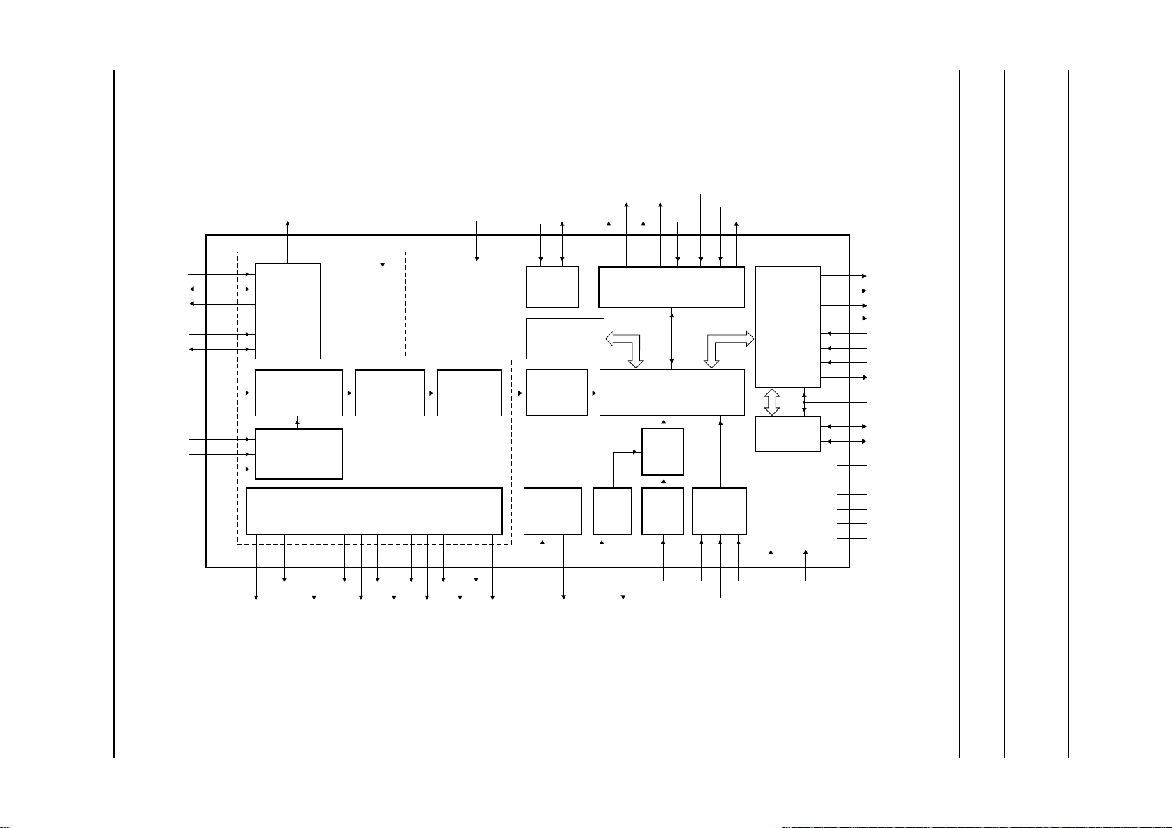
6 BLOCK DIAGRAM
7 PINNING
8 FUNCTIONAL DESCRIPTION
8.1 Video synchronization
8.2 CIF formatter
8.3 Compression engine
8.4 Transfer buffer
8.5 SNERT interface
8.6 Sensor pulse generator
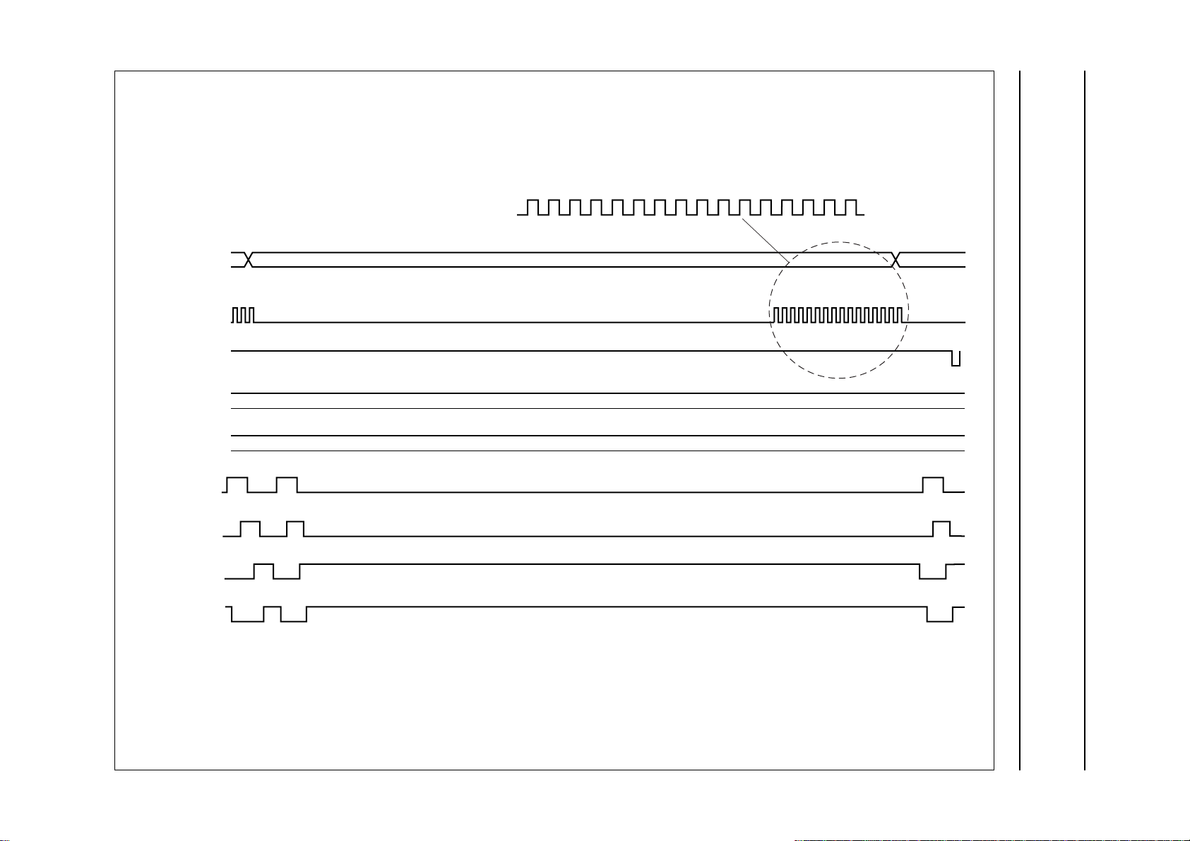
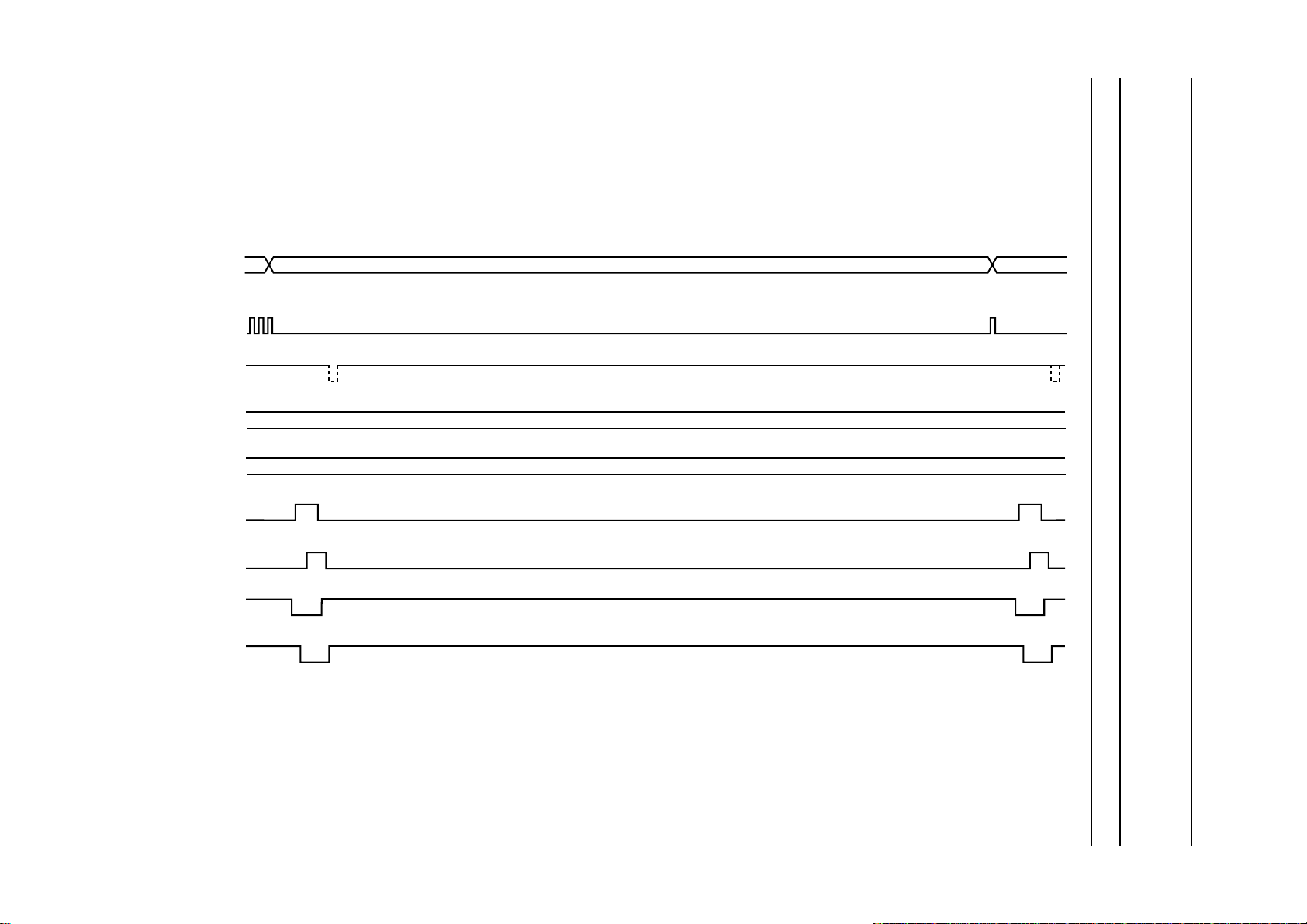
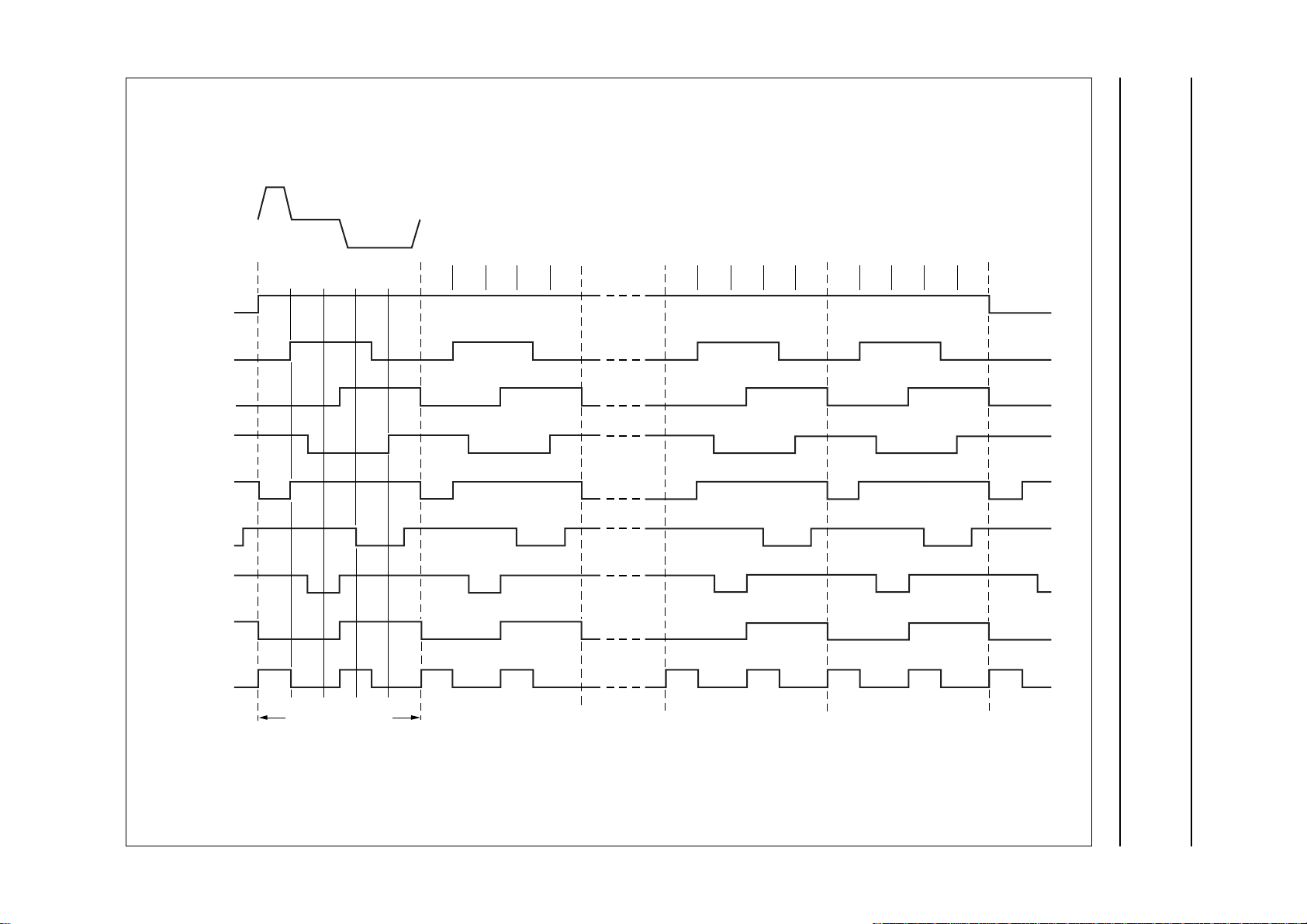
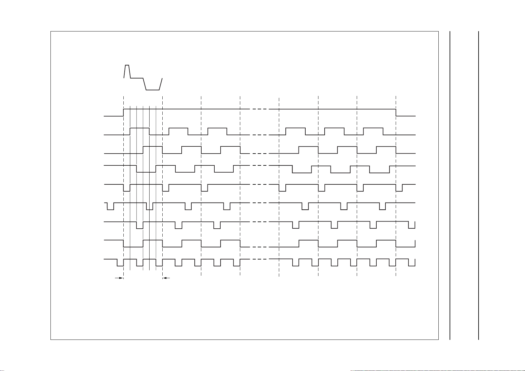
8.7 Pulse diagrams
8.8 USB video FIFO
8.9 PSIE-MMU, I2C-bus interface and USB RAM
space
8.10 ATX and external ATX interface
8.11 Audio
8.12 Power management
9 CONTROL REGISTER DESCRIPTION
9.1 SNERT (UART)
9.2 I2C-bus interface
9.2.1 Commands
9.2.2 End-points
9.2.3 Control top registers
9.2.4 Video FIFO registers
9.2.5 ADIF top registers
10 LIMITING VALUES
11 THERMAL CHARACTERISTICS
12 CHARACTERISTICS
13 TIMING
14 APPLICATION INFORMATION
15 PACKAGE OUTLINE
16 SOLDERING
16.1 Introduction to soldering surface mount
packages
16.2 Reflow soldering
16.3 Wave soldering
16.4 Manual soldering
16.5 Suitability of surface mount IC packages for
wave and reflow soldering methods
17 DEFINITIONS
18 LIFE SUPPORT APPLICATIONS
19 PURCHASE OF PHILIPS I2C COMPONENTS
1999 Apr 02 2
Page 3

Philips Semiconductors Product specification
Digital camera USB interface IC SAA8117HL
1 FEATURES
• Medium resolution CCD sensors (PAL non-interlaced
mode) or VGA CCD sensors (progressive mode)
• D1 digital video input (8 bits YUV 4 : 2 : 2,
time multiplexed)
• Internal Pulse Pattern Generator (PPG) dedicated for
medium resolution Sharp or compatible sensors and
VGA sensors and for frame rate selection
• Video formatter (programmable CIF formatter and
compression engine) controlled via SNERT (UART)
interface
• Selectable output frame rate (1 fps in VGA, up to 15 fps
in CIF format)
• Video packetizer FIFO
2
C-bus interface for communication between the USB
• I
protocol hardware and the external microcontroller
• Integrated analog bus driver (ATX)
• Microphone/audio input to USB (FGA, ADC, PLL and
decimator filter)
• Integrated analog bus driver (ATX)
• Integrated main oscillator
• Miscellaneous functions e.g. power management,
PLL backup oscillator.
2 APPLICATIONS
• Low-cost desktop video applications with USB interface.
3 GENERAL DESCRIPTION
The SAA8117HL is a monolithic integrated circuit which
can be used in PC video cameras to convert D1 video
signals and analog audio signals to properly formatted
USB packets.
It is designed as a back-end for the SAA8110G or
SAA8112HL (general camera digital processing ICs) and
is optimized for use with the TDA8784/87 (camera
pre-processing IC) and the 83C51RC (microcontroller).
4 ORDERING INFORMATION
TYPE
NUMBER
SAA8117HL LQFP100 plastic low profile quad flat package; 100 leads; body 14 × 14 × 1.4 mm SOT407-1
1999 Apr 02 3
NAME DESCRIPTION VERSION
PACKAGE
Page 4

Philips Semiconductors Product specification
Digital camera USB interface IC SAA8117HL
5 QUICK REFERENCE DATA
Measured over full voltage and operating temperature range.
SYMBOL PARAMETER CONDITIONS MIN. TYP. MAX. UNIT
V
DDD
V
DDA
I
DD(tot)
V
i(bus)
V
o(bus)
V
i(n)
V
o(n)
f
clk
P
tot
T
stg
T
amb
T
j
digital supply voltage 3.0 3.3 3.6 V
analog supply voltage 3.0 3.3 3.6 V
total supply current VDD= 3.3 V − 91 − mA
input voltage on I2C-bus interface pins 5 V tolerant TTL compatible V
output voltage on I2C-bus interface pin SDA 5 V tolerant TTL compatible V
input signal voltage on other pins 3.0V<VDD< 3.6 V low voltage TTL compatible V
output signal voltage on other pins 3.0V<VDD< 3.6 V low voltage TTL compatible V
clock frequency − 48 − MHz
total power dissipation T
=25°C − 300 − mW
amb
storage temperature −55 − +150 °C
operating ambient temperature 0 25 70 °C
junction temperature T
=70°C −40 − +125 °C
amb
1999 Apr 02 4
Page 5
This text is here in white to force landscape pages to be rotated correctly when browsing through the pdf in the Acrobat reader.This text is here in
n
_white to force landscape pages to be rotated correctly when browsing through the pdf in the Acrobat reader.This text is here inThis text is here in
white to force landscape pages to be rotated correctly when browsing through the pdf in the Acrobat reader. white to force landscape pages to be ...
1999 Apr 02 5
SMP
RESET
GENPOR
dbook, full pagewidth
SDA
SCL
CLOCK
UCINT
CLOCKON
UCPOR
SNAPSHOT
TRC
SUSREADYNOT
DCDCON
6 BLOCK DIAGRAM
Digital camera USB interface IC SAA8117HL
Philips Semiconductors Product specification
SNCL
SNDA
SNRES
RESERVED2
RESERVED1
YUV0
to
YUV7
HREF
VSYNC
LLC
56
55
57
53
52
35, 36,
37, 38,
42, 43
44, 45
49
50
47
SNERT
INTERFACE
AND HATCH
FORMATTER
SYNCHRONISATION
19, 18
17, 16
B1 to B4
A1 to A4
58
CIF
VIDEO
PATTERN PULSE GENERATOR
13, 12
23, 22,
11, 10
21
C1 to C3
COMPRESSION
24
RG
SHUTTER
(PPG)
20
SHP
51
ENGINE
28
SHD
29
CLK1
27
CLK2
SAA8117HL
TRANSFER
BUFFER
8
33
CLPDM
CLPOB30VD
76
31
9
HD
95
94
I2C-BUS
INTERFACE
USB
RAM SPACE
USB
VIDEO
FIFO
MAIN
OSCILLATOR
XIN1
XOUT1
93
AUDIO
PLL
65 87
86
XIN2
XOUT2
77
64
POWER
MANAGEMENT
AUDIO
ADC
AUDIO
AMP
MIC
96
PSIE
MMU
79
97100
99
2
S-BUS
I
INTERFACE
90
89
WS91BCK
DA
98
EXTERNAL
ATX
INTERFACE
ATX
70, 48, 41, 39
54, 34, 26, 14
88, 80, 78, 59, 4
92, 75, 69, 46, 40
3, 2, 1
REF1 to REF3
M0 to M2
32, 25, 15
85, 84, 62, 7
81, 82, 83
63
65
66
67
68
71
72
73
74
60
61
FCE130
SPEED
SUSPEND
VM
VP
RCV
VMO
VPO
OEBAR
ATXCTRL
ATXDP
ATXDM
V
to V
DD1
DD3
V
to V
DDA1
DDD1
to V
DDA4
DDD4
V
GND1 to GND4
AGND1 to AGND5
DGND1 to DGND5
Fig.1 Block diagram.
Page 6
Philips Semiconductors Product specification
Digital camera USB interface IC SAA8117HL
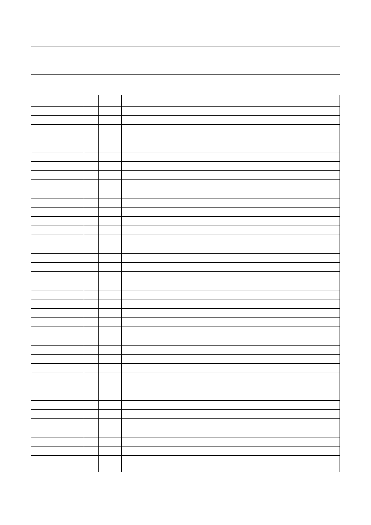
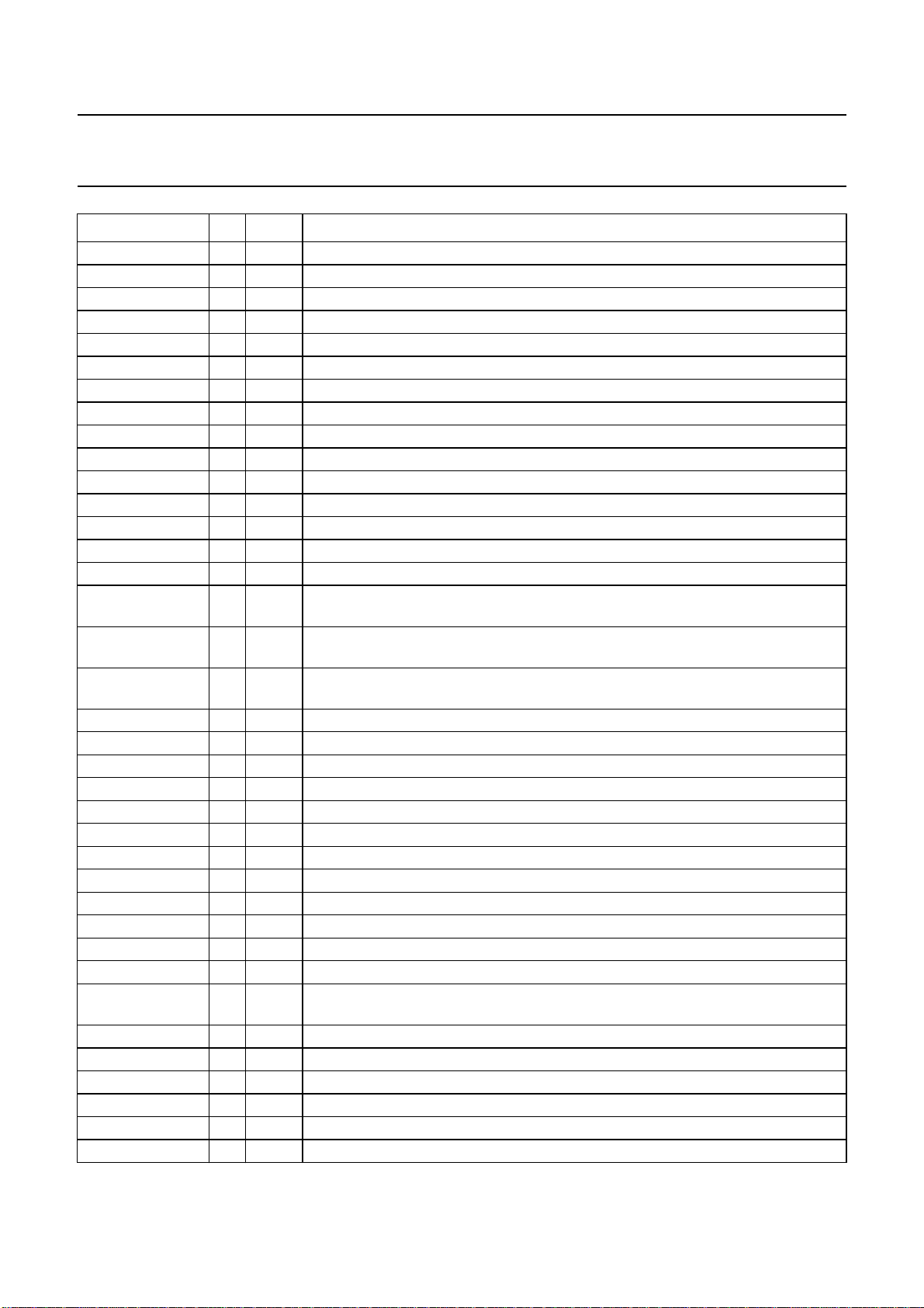
7 PINNING
SYMBOL PIN TYPE DESCRIPTION
M2 1 I test mode control signal bit 2
M1 2 I test mode control signal bit 1
M0 3 I test mode control signal bit 0
AGND1 4 P analog ground 1 for main oscillator (48 MHz, 3rd overtone)
XIN1 5 I oscillator input
XOUT1 6 O oscillator output
V
DDA1
CLPDM 8 O dummy clamp pulse output to TDA8784/87
CLPOB 9 O optical black clamp pulse output to TDA8784/87
B4 10 O vertical CCD load pulse output (VH1X)
B3 11 O vertical CCD load pulse output (VH3X)
B2 12 O vertical CCD load pulse output
B1 13 O vertical CCD load pulse output
GND1 14 P ground 1 for output buffers
V
DD1
A4 16 O vertical CCD transfer pulse output (V4X)
A3 17 O vertical CCD transfer pulse output (V3X)
A2 18 O vertical CCD transfer pulse output (V2X)
A1 19 O vertical CCD transfer pulse output (V1X)
SHUTTER 20 O shutter control output for CCD charge reset
C3 21 O horizontal CCD transfer pulse output
C2 22 O horizontal CCD transfer pulse output (FH1)
C1 23 O horizontal CCD transfer pulse output (FH2)
RG 24 O reset output for CCD output amplifier gate
V
DD2
GND2 26 P ground 2 for output buffers
CLK1 27 O pixel clock output to TDA8784/87and SAA8110G
SHP 28 O preset sample-and-hold pulse output to TDA8784/87 (FCDS)
SHD 29 O data sample-and-hold pulse output to TDA8784/87 (FS)
VD 30 O vertical definition pulse output to SAA8110G
HD 31 O horizontal definition pulse output to SAA8110G
V
DD3
CLK2 33 O double pixel clock output to SAA8110G
GND3 34 P ground 3 for output buffers
YUV0 35 I multiplexed input YUV-bit 0 (LSB)
YUV1 36 I multiplexed input YUV-bit 1 input
YUV2 37 I multiplexed input YUV-bit 2 input
YUV3 38 I multiplexed input YUV-bit 3 input
V
DDD1
7 P analog supply voltage 1 for main oscillator (48 MHz, 3rd overtone)
15 P supply voltage 1 for output buffers
25 P supply voltage 2 for output buffers
32 P supply voltage 3 for output buffers
39 P digital supply voltage 1 for input buffers and predrivers and one part of the digital
core
1999 Apr 02 6
Page 7
Philips Semiconductors Product specification
Digital camera USB interface IC SAA8117HL
SYMBOL PIN TYPE DESCRIPTION
DGND1 40 P digital ground 1 for input buffers and predrivers and for the digital core
V
DDD2
YUV4 42 I multiplexed input YUV-bit 4
YUV5 43 I multiplexed input YUV-bit 5
YUV6 44 I multiplexed input YUV-bit 6
YUV7 45 I multiplexed input YUV-bit 7
DGND2 46 P digital ground 2 for input buffers and predrivers and for the digital core
LLC 47 I line-locked clock input (delayed CLK2) for YUV-port from SAA8110G
V
DDD3
HREF 49 I horizontal reference input for YUV-port from SAA8110G
VSYNC 50 I vertical synchronization input for YUV-port from SAA8110G
RESET 51 I Power-on reset input (for video processing and PPG)
RESERVED1 52 − test pin (should not be used)
RESERVED2 53 − test pin (should not be used)
GND4 54 P ground 4 for output buffer
SNDA 55 I/O data I/O for SNERT-interface (communication between SAA8117HL and
SNCL 56 I input clock for SNERT-interface (communication between SAA8117HL and
SNRES 57 O output reset for SNERT-interface (communication between SAA8117HL and
SMP 58 O output switch mode pulse for DC-to-DC power supply
AGND2 59 P analog ground 2 for ATX (transceiver)
ATXDP 60 I/O positive driver of the differential data pair input/output (ATX)
ATXDM 61 I/O negative driver of the differently data pair input/output (ATX)
V
DDA2
SPEED 63 O required output for ATX-backup solution
UCINT 64 O interrupt output from USB protocol hardware to microcontroller
SUSPEND 65 O control output from USB protocol hardware to microcontroller
VM 66 O required output for ATX-backup solution (txdn)
VP 67 O required output for ATX-backup solution (txdp)
RCV 68 I required output for ATX-backup solution
DGND3 69 P digital ground 3 for input buffers and predrivers and for the digital core
V
DDD4
VMO 71 I required input or ATX-backup solution (rxdn)
VPO 72 I required input for ATX-backup solution (rxdp)
OEBAR 73 O required output for ATX-backup solution
ATXCTRL 74 I required input for ATX-backup solution
DGND4 75 P digital ground 4 for input buffers and predrivers and for the digital core
GENPOR 76 I Power-on reset input (for USB protocol hardware)
41 P digital supply voltage 2 for digital core
48 P digital supply voltage 3 for digital core
SAA8110G)
SAA8110G)
SAA8110G)
62 P analog supply voltage 2 for ATX
70 P digital supply voltage 4 for one part of input buffers and predrivers and for the
digital core
1999 Apr 02 7
Page 8

Philips Semiconductors Product specification
Digital camera USB interface IC SAA8117HL
SYMBOL PIN TYPE DESCRIPTION
UCPOR 77 O output control from USB protocol hardware to microcontroller
AGND3 78 P analog ground 3 for FGA
MIC 79 I microphone input
AGND4 80 P analog ground 4 for FGA/ADC
REF1 81 I reference input voltage 1 for FGA/ADC (double-bonding)
REF2 82 I reference input voltage 2 for DACn (used in the ADC)
REF3 83 I reference input voltage 3 for DACp (used in the ADC)
V
DDA3
V
DDA4
XIN2 86 I oscillator input required for PLL backup solution
XOUT2 87 O oscillator output required for PLL backup solution
AGND5 88 P analog ground 5 for PLL
WS 89 I I
DA 90 I I
BCK 91 I I
DGND5 92 P digital ground 5 for input buffers and predrivers and for the digital core
CLOCK 93 O clock output from USB protocol hardware to microcontroller
SCL 94 I slave I
SDA 95 I/O slave I
CLOCKON 96 O control output for main oscillator switched on
SNAPSHOT 97 I input for remote wake-up (snapshot)
DCDCON 98 O control output from USB protocol hardware to power supply module
SUSREADYNOT 99 I input from microcontroller for SUSPEND mode
TRC 100 I threshold control input for enabling the clock (switching for power management)
84 P analog supply voltage 3 for FGA/ADC
85 P analog supply voltage 4 for PLL
2
S-bus word select (required for FGA/ADC backup solution)
2
S-bus data (required for FGA/ADC backup solution)
2
S-bus clock (required for FGA/ADC backup solution)
2
C-bus clock input
2
C-bus data input/output
1999 Apr 02 8
Page 9
Philips Semiconductors Product specification
Digital camera USB interface IC SAA8117HL
handbook, full pagewidth
DDA3
XOUT2
XIN2
DDD4
V
REF2
REF1
AGND4
8079787776
UCPOR
GENPOR
75
74
73
72
71
70
69
68
67
66
65
64
63
62
61
60
59
58
57
56
55
54
53
52
51
DGND4
ATXCTRL
OEBAR
VPO
VMO
V
DDD4
DGND3
RCV
VP
VM
SUSPEND
UCINT
SPEED
V
DDA2
ATXDM
ATXDP
AGND2
SMP
SNRES
SNCL
SNDA
GND4
RESERVED2
RESERVED1
RESET
V
REF3
MIC
AGND3
M2
M1
M0
AGND1
XIN1
XOUT1
V
DDA1
CLPDM
CLPOB
B4
B3
B2
B1
GND1
V
DD1
A4
A3
A2
A1
SHUTTER
C3
C2
C1
RG
V
DD2
TRC
SUSREADYNOT
DCDCON
SNAPSHOT
CLOCKON
SDA
SCL
CLOCK
DGND5
BCKDAWS
99989796959493929190898887868584838281
100
1
2
3
4
5
6
7
8
9
10
11
12
13
14
15
16
17
18
19
20
21
22
23
24
25
AGND5
SAA8117HL
26
GND2
CLK1
SHP
31323334353637383940414243444546474849
VD
HD
SHD
DD3
V
CLK2
GND3
YUV0
YUV1
YUV2
30
29
28
27
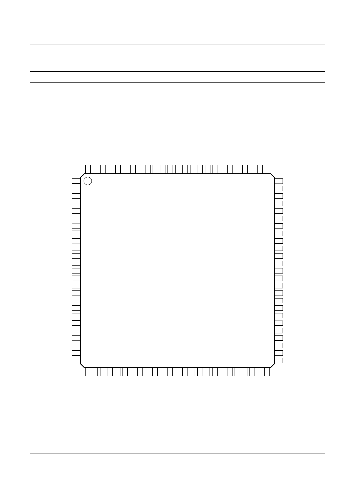
Fig.2 Pin configuration.
1999 Apr 02 9
YUV3
DDD1
V
DDD2
V
DGND1
YUV4
YUV5
YUV6
YUV7
LLC
DGND2
DDD3
V
HREF
50
FCE131
VSYNC
Page 10

Philips Semiconductors Product specification
Digital camera USB interface IC SAA8117HL
8 FUNCTIONAL DESCRIPTION
8.1 Video synchronization
The video synchronization module (see Fig.1) is capable
of locking onto the video signal thereby implementing a
horizontal gate signal HREF (HREF = HIGH when data is
valid) and a VS signal indicating the start of a new video
frame. This module expects, in the PAL mode, 288 active
lines from a total of 292 lines and in the VGA mode,
480 active lines from a total of 486 lines. The module
generates control signals for the CIF formatter.
8.2 CIF formatter
The video data must be progressive (or non-interlaced)
and in 4 :2:2(UYVY) format. The CIF formatter module
(see Figs 1 and 3) is programmable to perform down
scaling from 512 × 288 (PAL mode) or 640 × 480 (VGA
mode) to 352 × 288 or 176 × 144 without affecting the
aspect ratio.
The horizontal scaling is achieved with a Variable Phase
Delay filter (VPD-4). To avoid aliasing, this module also
contains a prefilter which has three modes:
• Prefilter A (3 taps)
• Prefilter B (7 taps)
• Prefilter B-comb (13 taps).
Prefilter B-comb is similar to prefilter B, but inserts extra
taps with amplification 0.
This prefilter must be chosen by selecting prefilter B and
setting SN_Prefilter_B_Comb. Prefilter B-comb can be
used independently from prefilter A.
The incoming 4:2:2 data is vertically filtered to 4 : 2 : 0
by throwing away colour samples. In the even lines the
V-samples are discarded, in the odd lines the U-samples.
The vertical scaling in PAL mode is from CIF (352 × 288)
to QCIF (176 × 144) only. This is done via a vertical
prefilter A (3 taps). In VGA mode a VPD-4 vertical filter is
applied to scale from 640 × 480 to CIF and QCIF.
From the QCIF image a sub-QCIF cut (128 × 96) can be
made. Due to the granularity of the cropping origin, a
UV interchange can occur. This interchange can be
corrected with SN_EIRRAH.
In VGA mode the CIF formatter can be bypassed to create
a full resolution snapshot. The snapshot can be in 4 :2:0
and in 4 :2:2 format, selectable with SN_4 :2:2.
8.3 Compression engine
The compression engine module (see Figs 1 and 3) works
on CIF format only. The CIF data is compressed to a fixed
number of bytes per frame. This number can be selected
leading a compression factor of either 3 or 4. As a result
the data stream of CIF4:2:0 equals the data stream of
QCIF 4:2:2 (3times compression) or QCIF 4:2:0
(4 times compression). The algorithm is Philips
proprietary. Real-time decoding can be done in software
on any Pentium platform.
handbook, full pagewidth
YUV0 to YUV7
SN_Prefilter A_On/Off
PREFILTER
A
PREFILTER
SN_Prefilter B_On/Off
SN_Prefilter B_Comb
SN_Output_Format_Select
B
Fig.3 The CIF formatter and compression engine.
1999 Apr 02 10
SN_4:2:2
SN_EIRRAH
SN_PAL_VGA
DOWN
SCALER
COMPRESSION
ENGINE
SN_Compress
SN_Compression_Ratio
SN_Clk_Compress_On
FCE132
to
transfer
buffer
Page 11

Philips Semiconductors Product specification
Digital camera USB interface IC SAA8117HL
8.4 Transfer buffer
The transfer buffer module (see Fig.1) ensures a smooth
transfer of the data to the FIFO of the USB. Moreover the
transfer buffer can insert in band synchronization words in
the video data stream.
This function can be switched on and off with
SN_In band_Control in register CONTROL17_0.
The synchronization words can only be used with
non-compressed data streams and are formatted like
0x00 0xFF 0x<framecounter>7<linecounter>9.
The subscript denotes the number of bits and the frame
counter is circular incrementing.
The non-compressed data is formatted like:
4:2:0:<optional sync word><Y0><Y1><Y2><Y3>
<C0><C2><Y4><Y5><Y6><Y7><C4><C6>....,
4:2:2: <optional sync word><Y0><Y1><Y2><Y3>
<U0><V0><U2><V2><Y4>....,
where C denotes U-data in the even lines (0, 2, 4, etc.)
and V-data in the odd lines (1, 3, 5, etc.).
8.5 SNERT interface
In a USB camera the SAA8110G will operate on a clock
frequency which depends on the actual frame rate. For the
slowest frame rates, this frequency can be so low that the
SNERT communication is no longer functional over the
specified entire frequency range of the microcontroller.
The microcontroller must adapt its SNERT bus frequency
to a frequency appropriate for the current mode in which
the SAA8110G is operating.
It should be noted that in case of medium resolution Sharp
or compatible sensors an external inverter driver is
required to convert the 3 V pulses into a voltage suitable
for the used CCD sensor. For the medium resolution Sharp
CCD sensor driver, the name of the pins to which the PPG
pulses must be connected are indicated between brackets
in the SAA8117HL pinning list (pins C3, B1 and B2 are not
used).
For both type of sensors the PPG generates 8 different
frame rates (see Table 6). The active video size is
512 × 288 for PAL and 640 × 480 for VGA. The total H × V
size is 685 × 292 for PAL and 823 × 486 for VGA.
It should be noted that additional HD pulses are added
during the vertical blanking interval to reach a total of
312 lines in PAL mode and 525 lines in VGA mode as
required by the SAA8110G.
The following registers are associated with the PPG:
• CONTROL17_0
• CONTROL17_2
• PPG_SHUTTERSPEED_0
• PPG_SHUTTERSPEED_1
• PPG_CLPOB_START_LSB
• PPG_CLPOB_STOP_LSB
• PPG_CLPDM_START_LSB
• PPG_CLPDM_STOP_LSB
• CLPMSB.
8.7 Pulse diagrams
The SAA8117HL itself is also partly controlled via SNERT.
The CIF formatter, compression engine and the PPG
function are controlled via SNERT. This SNERT interface
works independently from the frame rate and can always
be operated in the full frequency range.
8.6 Sensor pulse generator
The SAA8117HL incorporates a Pulse Pattern Generator
(PPG) function. The PPG can be used for PAL medium
resolution Sharp sensors (LZ2423) or compatible CCD
sensors. The SAA8117HL can also handle VGA type CCD
sensors, so a set of pulses is provided to simplify the use
of such sensors. Depending on the type of sensor, it will be
necessary to reformat these pulses externally according to
the sensor specification.
1999 Apr 02 11
For medium resolution CCD sensors (PAL):
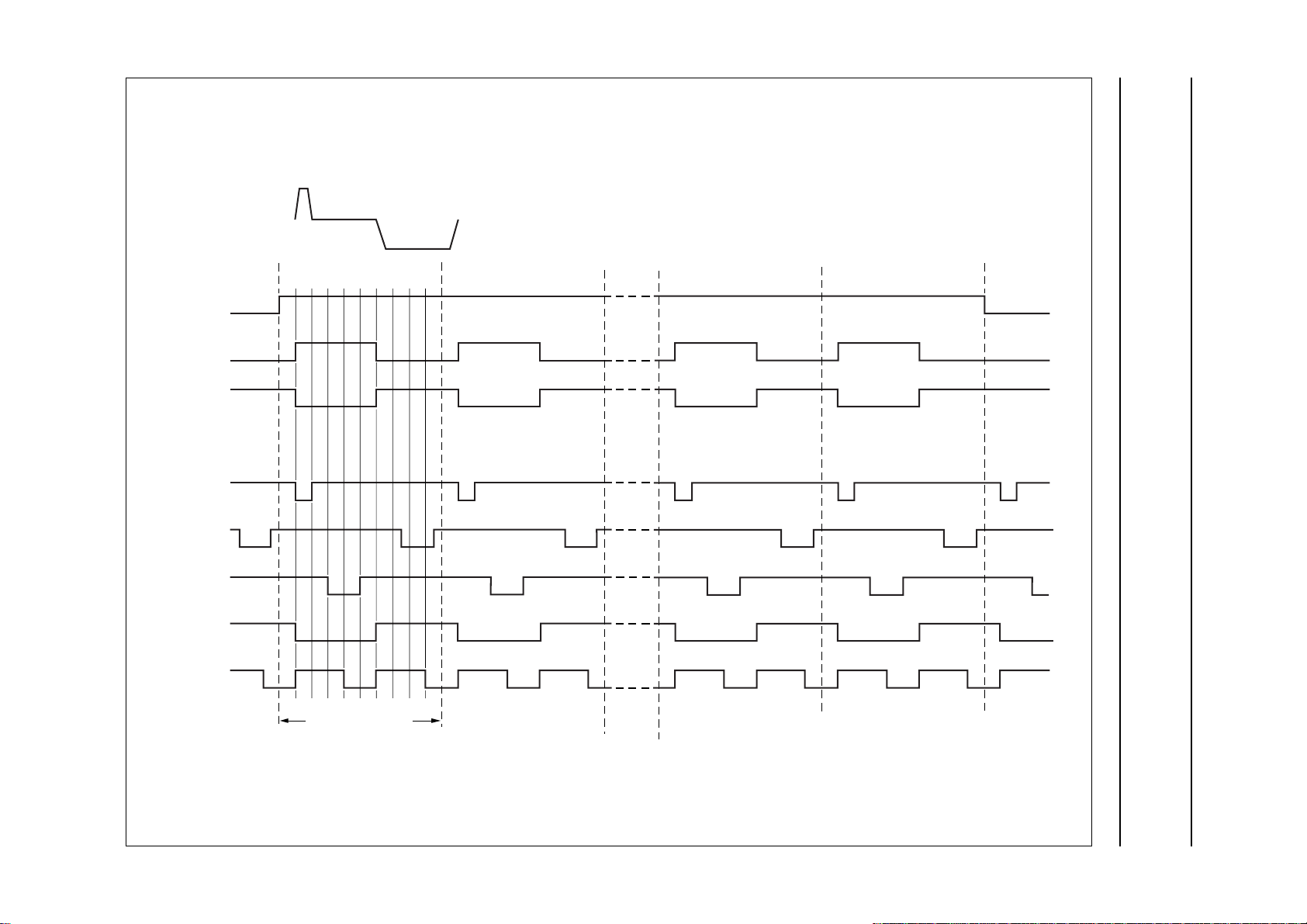
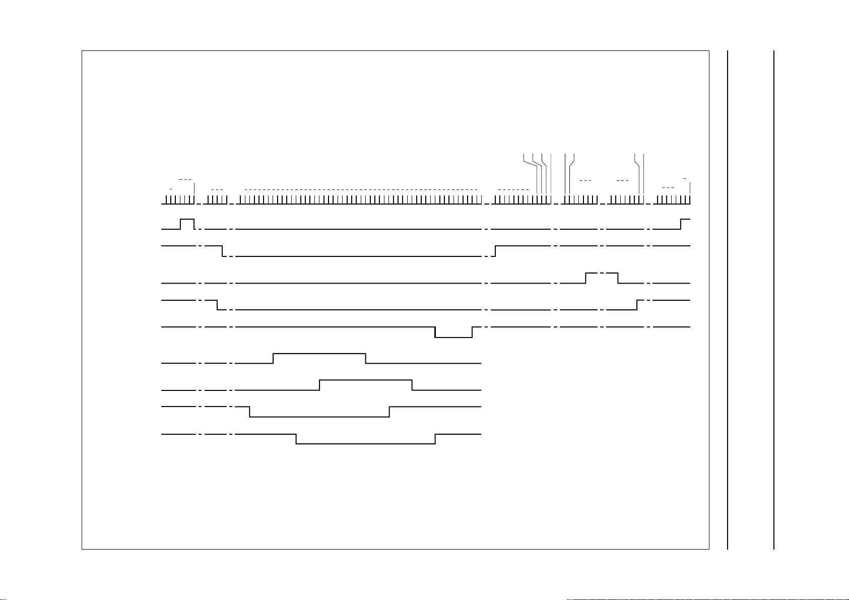
• High-speed pulses, see Figs 4 and 5
• Horizontal pulses, see Fig.6
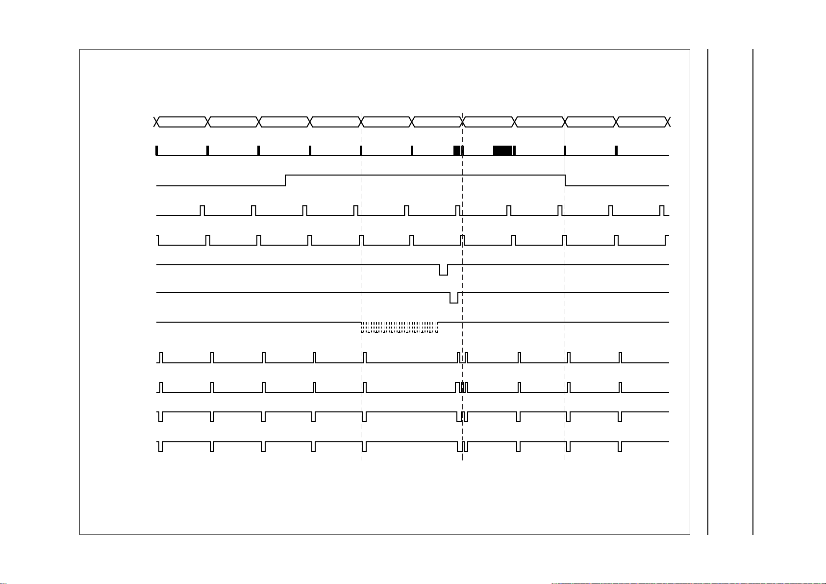
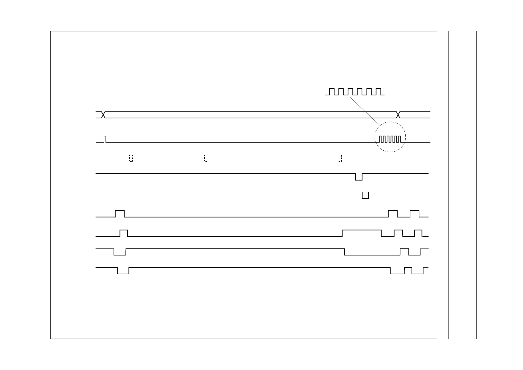
• Vertical pulses, see Figs 7 to 11.
For VGA-sensors:
• High-speed pulses, see Figs 12 to 14
• Horizontal pulses, see Fig.15
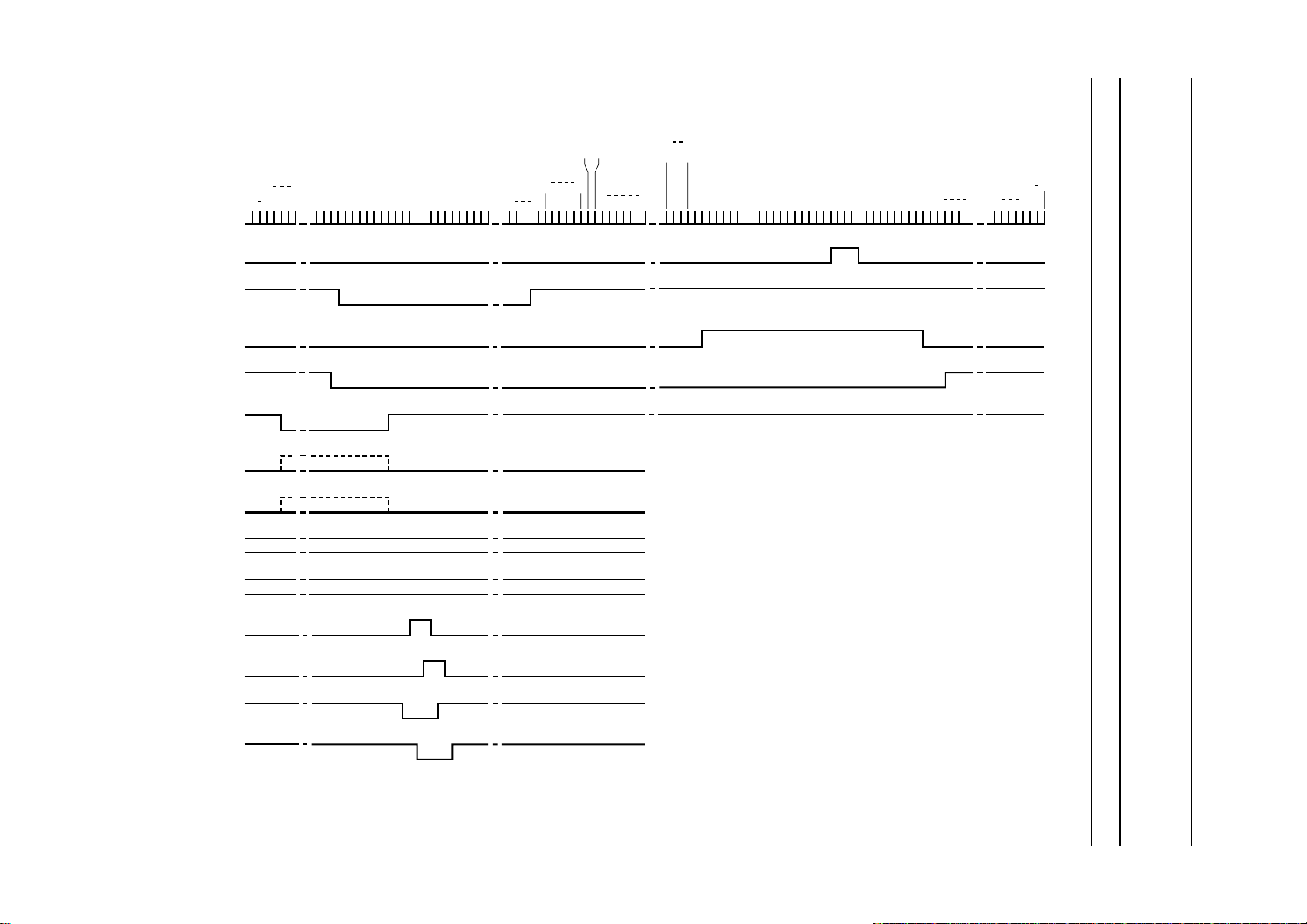
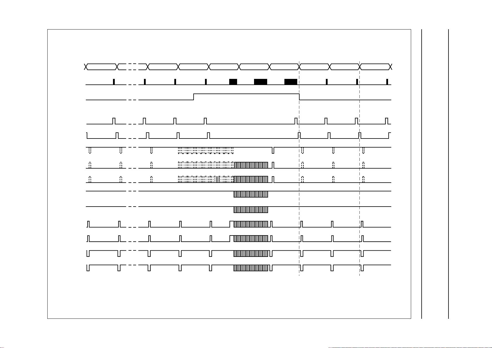
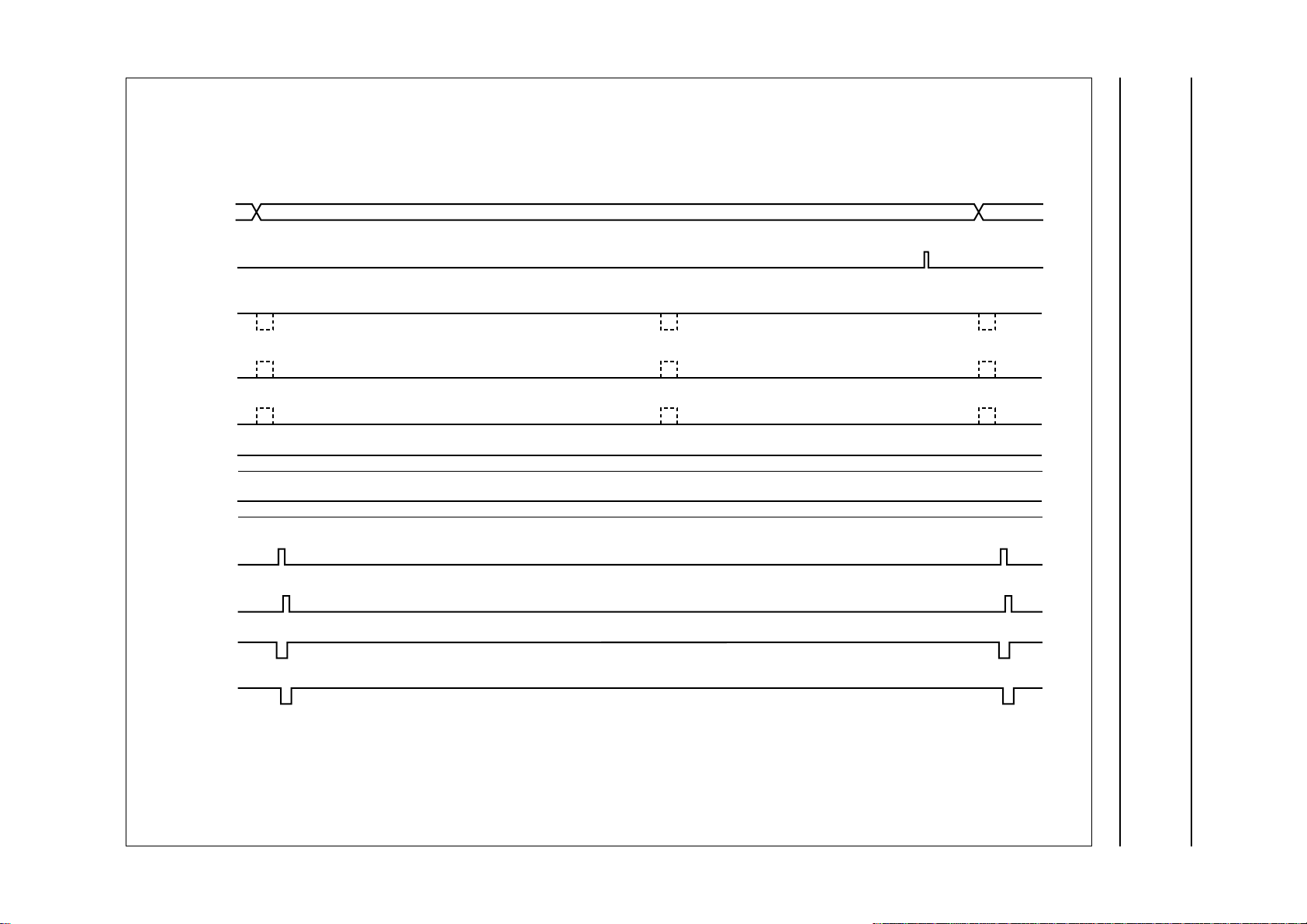
• Vertical pulses, see Figs 16 to 21.
Page 12
This text is here in white to force landscape pages to be rotated correctly when browsing through the pdf in the Acrobat reader.This text is here in
_white to force landscape pages to be rotated correctly when browsing through the pdf in the Acrobat reader.This text is here inThis text is here in
white to force landscape pages to be rotated correctly when browsing through the pdf in the Acrobat reader. white to force landscape pages to be ...
1999 Apr 02 12
CCD OUTPUT
02461357802491356879 900 2461357802491356879
CLOCK ENABLE
C1 (FH1)
C2 (FH2)
handbook, full pagewidth
Philips Semiconductors Product specification
Digital camera USB interface IC SAA8117HL
RG (FR)
SHD (FS)
SHP(FCDS)
CLK1
CLK2
mode 0: 1/(4.8 MHz)
FCE133
Fig.4 High-speed pulses for PAL medium resolution (1).
Page 13

This text is here in white to force landscape pages to be rotated correctly when browsing through the pdf in the Acrobat reader.This text is here in
_white to force landscape pages to be rotated correctly when browsing through the pdf in the Acrobat reader.This text is here inThis text is here in
white to force landscape pages to be rotated correctly when browsing through the pdf in the Acrobat reader. white to force landscape pages to be ...
1999 Apr 02 13
CCD OUTPUT
012301230 301230123
CLOCK ENABLE
C1 (FH1)
C2 (FH2)
RG (FR)
handbook, full pagewidth
Philips Semiconductors Product specification
Digital camera USB interface IC SAA8117HL
SHD (FS)
SHP (FCDS)
CLK1
CLK2
mode 1: 1/(4 MHz)
mode 2: 1/(3 MHz)
mode 3: 1/(2.4 MHz)
mode 4: 1/(2 MHz)
mode 5: 1/(1.5 MHz)
mode 6: 1/(1 MHz)
mode 7: 1/(750 kHz)
FCE134
Fig.5 High-speed pulses for PAL medium resolution (2).
Page 14
This text is here in white to force landscape pages to be rotated correctly when browsing through the pdf in the Acrobat reader.This text is here in
_white to force landscape pages to be rotated correctly when browsing through the pdf in the Acrobat reader.This text is here inThis text is here in
white to force landscape pages to be rotated correctly when browsing through the pdf in the Acrobat reader. white to force landscape pages to be ...
1999 Apr 02 14
handbook, full pagewidth
100 BLK
101 BLK
102 A1
103 A2
612 A511
613 A512
642
Philips Semiconductors Product specification
Digital camera USB interface IC SAA8117HL
643
HD
CLOCK ENABLE
CLPOB
CLPDM
SHUTTER (OFDX)
A1 (V1X)
A2 (V2X)
A3 (V3X)
A4 (V4X)
4
614 BLK
619 BLK
636 BLK
685/0
683
14 0
12
22
16
15
(1)
64 72
29 49
39 59
24
34 64
54
91
74
91
99
(1) (1)
641 BLK
(1)
680
2
685/0
FCE135
(1) CLPOB and CLPDM are programmable.
Fig.6 Horizontal pulses for PAL medium resolution.
Page 15
This text is here in white to force landscape pages to be rotated correctly when browsing through the pdf in the Acrobat reader.This text is here in
_white to force landscape pages to be rotated correctly when browsing through the pdf in the Acrobat reader.This text is here inThis text is here in
white to force landscape pages to be rotated correctly when browsing through the pdf in the Acrobat reader. white to force landscape pages to be ...
handbook, full pagewidth
1999 Apr 02 15
Philips Semiconductors Product specification
Digital camera USB interface IC SAA8117HL
INE#
HD
VD
CLPOB (DCP)
CLPDM (BCP)
B4 (VH1X)
B3 (VH3X)
SHUTTER (OFDX)
A1 (V1X)
A2 (V2X)
A285
289
A286
290
A287
291
A288
292
Hd
Hd
1
2
AL1
3
AL2
4
A1
A2
5
6
A3 (V3X)
A4 (V4X)
FCE136
Fig.7 Vertical pulses for PAL medium resolution (1).
Page 16

This text is here in white to force landscape pages to be rotated correctly when browsing through the pdf in the Acrobat reader.This text is here in
_white to force landscape pages to be rotated correctly when browsing through the pdf in the Acrobat reader.This text is here inThis text is here in
white to force landscape pages to be rotated correctly when browsing through the pdf in the Acrobat reader. white to force landscape pages to be ...
1999 Apr 02 16
handbook, full pagewidth
Philips Semiconductors Product specification
Digital camera USB interface IC SAA8117HL
INE#
HD
SHUTTER (OFDX)
B4 (VH1X)
B3 (VH3X)
A1 (V1X)
A2 (V2X)
A3 (V3X)
A4 (V4X)
292 1 2
1
4
64
72
29
49
39
59
24
54
34
64
1
4
29
24
34
49
39
54
FCE137
59
64
Fig.8 Vertical pulses for PAL medium resolution (2).
Page 17
This text is here in white to force landscape pages to be rotated correctly when browsing through the pdf in the Acrobat reader.This text is here in
_white to force landscape pages to be rotated correctly when browsing through the pdf in the Acrobat reader.This text is here inThis text is here in
white to force landscape pages to be rotated correctly when browsing through the pdf in the Acrobat reader. white to force landscape pages to be ...
1999 Apr 02 17
handbook, full pagewidth
647
651
655
659
663
667
671
675
679
14683
Philips Semiconductors Product specification
Digital camera USB interface IC SAA8117HL
INE#
HD
SHUTTER (OFDX)
B4 (VH1X)
B3 (VH3X)
A1 (V1X)
A2 (V2X)
A3 (V3X)
A4 (V4X)
1
1
4
64
72
RESET_DATA [9 to 0] + 8RESET_DATA [9 to 0]
29
49
39
59
24
54
34
64
2 3
1
4
545
553
584
599
599
614
664
684
29
674
669
9
4
24
14
34
554
559
644
49
39
54
FCE138
59
64
Fig.9 Vertical pulses for PAL medium resolution (3).
Page 18
This text is here in white to force landscape pages to be rotated correctly when browsing through the pdf in the Acrobat reader.This text is here in
_white to force landscape pages to be rotated correctly when browsing through the pdf in the Acrobat reader.This text is here inThis text is here in
white to force landscape pages to be rotated correctly when browsing through the pdf in the Acrobat reader. white to force landscape pages to be ...
1999 Apr 02 18
handbook, full pagewidth
579
575
571
567
583
587
591
595
599
603
607
611
615
619
623
627
631
635
639
643
647
651
655
659
663
667
671
675
679
14683
Philips Semiconductors Product specification
Digital camera USB interface IC SAA8117HL
INE#
HD
SHUTTER (OFDX)
B4 (VH1X)
B3 (VH3X)
A1 (V1X)
A2 (V2X)
A3 (V3X)
A4 (V4X)
2
664
669
674
1
684
3 4
4
29
49
9
4
59
39
24
54
14
34
64
1
4
64
72
29
49
59
39
24
54
34
64
FCE139
Fig.10 Vertical pulses for PAL medium resolution (4).
Page 19
This text is here in white to force landscape pages to be rotated correctly when browsing through the pdf in the Acrobat reader.This text is here in
_white to force landscape pages to be rotated correctly when browsing through the pdf in the Acrobat reader.This text is here inThis text is here in
white to force landscape pages to be rotated correctly when browsing through the pdf in the Acrobat reader. white to force landscape pages to be ...
1999 Apr 02 19
handbook, full pagewidth
Philips Semiconductors Product specification
Digital camera USB interface IC SAA8117HL
INE#
HD
SHUTTER (OFDX)
B4 (VH1X)
B3 (VH3X)
A1 (V1X)
A2 (V2X)
A3 (V3X)
A4 (V4X)
3 4 5
1
4
64
72
29
49
39
59
24
54
34
64
1
4
29
24
34
49
39
54
FCE140
64
72
59
64
Fig.11 Vertical pulses for PAL medium resolution (5).
Page 20
This text is here in white to force landscape pages to be rotated correctly when browsing through the pdf in the Acrobat reader.This text is here in
_white to force landscape pages to be rotated correctly when browsing through the pdf in the Acrobat reader.This text is here inThis text is here in
white to force landscape pages to be rotated correctly when browsing through the pdf in the Acrobat reader. white to force landscape pages to be ...
1999 Apr 02 20
CCD OUTPUT
0123401234 40021 4013 234
CLOCK ENABLE
C1
C2
C3
handbook, full pagewidth
Philips Semiconductors Product specification
Digital camera USB interface IC SAA8117HL
RG
SHD
SHP
CLK1
CLK2
mode 0: 1/(9.6 MHz)
FCE141
Fig.12 High-speed pulses for VGA sensors (1).
Page 21
This text is here in white to force landscape pages to be rotated correctly when browsing through the pdf in the Acrobat reader.This text is here in
n
_white to force landscape pages to be rotated correctly when browsing through the pdf in the Acrobat reader.This text is here inThis text is here in
white to force landscape pages to be rotated correctly when browsing through the pdf in the Acrobat reader. white to force landscape pages to be ...
1999 Apr 02 21
CCD OUTPUT
0240135124023513405 0245135024013512435
CLOCK ENABLE
C1
C2
C3
dbook, full pagewidth
Philips Semiconductors Product specification
Digital camera USB interface IC SAA8117HL
RG
SHD
SHP
CLK1
CLK2
mode 1: 1/(8 MHz)
mode 3: 1/(4 MHz)
FCE142
Fig.13 High-speed pulses for VGA sensors (2).
Page 22
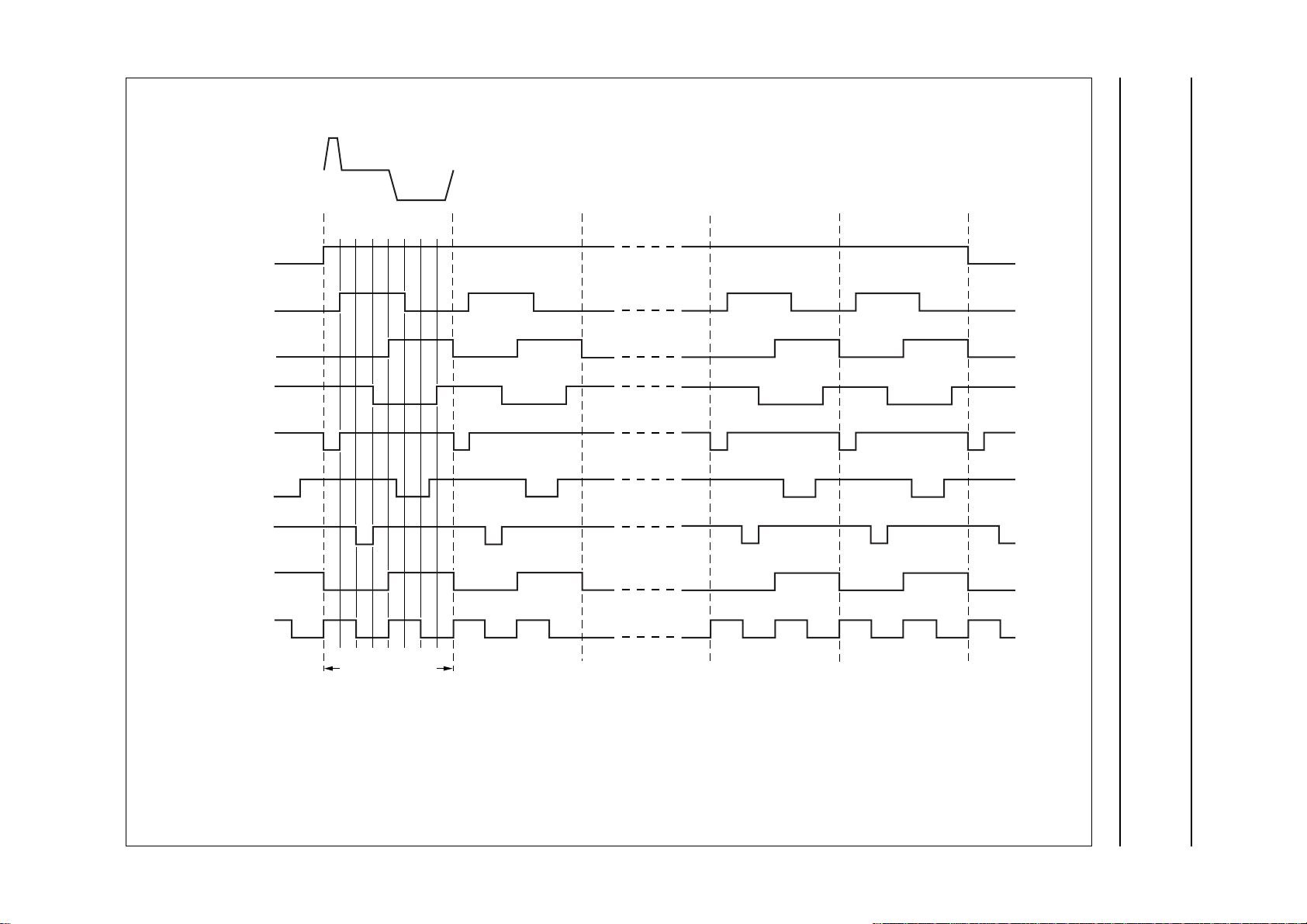
This text is here in white to force landscape pages to be rotated correctly when browsing through the pdf in the Acrobat reader.This text is here in
n
_white to force landscape pages to be rotated correctly when browsing through the pdf in the Acrobat reader.This text is here inThis text is here in
white to force landscape pages to be rotated correctly when browsing through the pdf in the Acrobat reader. white to force landscape pages to be ...
1999 Apr 02 22
CCD OUTPUT
02461357024613570 02713460257134657
CLOCK ENABLE
C1
C2
C3
RG
dbook, full pagewidth
Philips Semiconductors Product specification
Digital camera USB interface IC SAA8117HL
SHD
SHP
CLK1
CLK2
mode 2: 1/(6 MHz)
mode 4: 1/(3 MHz)
mode 5: 1/(2 MHz)
mode 6: 1/(1.5 MHz)
mode 7: 1/(1 MHz)
FCE143
Fig.14 High-speed pulses for VGA sensors (3).
Page 23
This text is here in white to force landscape pages to be rotated correctly when browsing through the pdf in the Acrobat reader.This text is here in
n
_white to force landscape pages to be rotated correctly when browsing through the pdf in the Acrobat reader.This text is here inThis text is here in
white to force landscape pages to be rotated correctly when browsing through the pdf in the Acrobat reader. white to force landscape pages to be ...
1999 Apr 02 23
dbook, full pagewidth
Philips Semiconductors Product specification
Digital camera USB interface IC SAA8117HL
HD
CLOCK ENABLE
CLPOB
CLPDM
SHUTTER
A1
A2
A3
A4
B1
B2
B3
B4
4
821
823/0
12
15
(1)
2 22
222
222
25 28
27 30
24 29
26 31
65 D
60
36
64
63
71 BLK
70 D
72 BLK
73 A1
79 A7
728 A656
731 A659
732 BLK
751 755
(1) (1)
767
766 BLK
(1)
771
818
2
823/0
FCE144
(1) CLPOB and CLPDM are programmable.
Fig.15 Horizontal pulses for VGA sensors.
Page 24
This text is here in white to force landscape pages to be rotated correctly when browsing through the pdf in the Acrobat reader.This text is here in
n
_white to force landscape pages to be rotated correctly when browsing through the pdf in the Acrobat reader.This text is here inThis text is here in
white to force landscape pages to be rotated correctly when browsing through the pdf in the Acrobat reader. white to force landscape pages to be ...
1999 Apr 02 24
dbook, full pagewidth
Philips Semiconductors Product specification
Digital camera USB interface IC SAA8117HL
INE#
HD
VD
CLPOB
CLPDM
SHUTTER
A1
A2
A3
A4
B1
A476
482
A480
483 485 486
Hd
1
Hd
Hd
2
3
Hd
AL1
4
5
AL2
6
A1
7
B2
B3
B4
FCE145
Fig.16 Vertical pulses for VGA sensors (1).
Page 25
This text is here in white to force landscape pages to be rotated correctly when browsing through the pdf in the Acrobat reader.This text is here in
n
_white to force landscape pages to be rotated correctly when browsing through the pdf in the Acrobat reader.This text is here inThis text is here in
white to force landscape pages to be rotated correctly when browsing through the pdf in the Acrobat reader. white to force landscape pages to be ...
1999 Apr 02 25
dbook, full pagewidth
Philips Semiconductors Product specification
Digital camera USB interface IC SAA8117HL
INE#
HD
SHUTTER
A1
A2
A3
A4
B1
B2
B3
486 1 2
751
755
2
22
RESET_DATA [9 to 0] + 20RESET_DATA [9 to 0]
2
22
2
22
25
28
27
30
24
29
RESET_DATA [9 to 0] + 20RESET_DATA [9 to 0]
RESET_DATA [9 to 0] + 20RESET_DATA [9 to 0]
2
22
2
22
2
22
25
27
24
28
30
29
B4
26
31
26
FCE146
31
Fig.17 Vertical pulses for VGA sensors (2).
Page 26
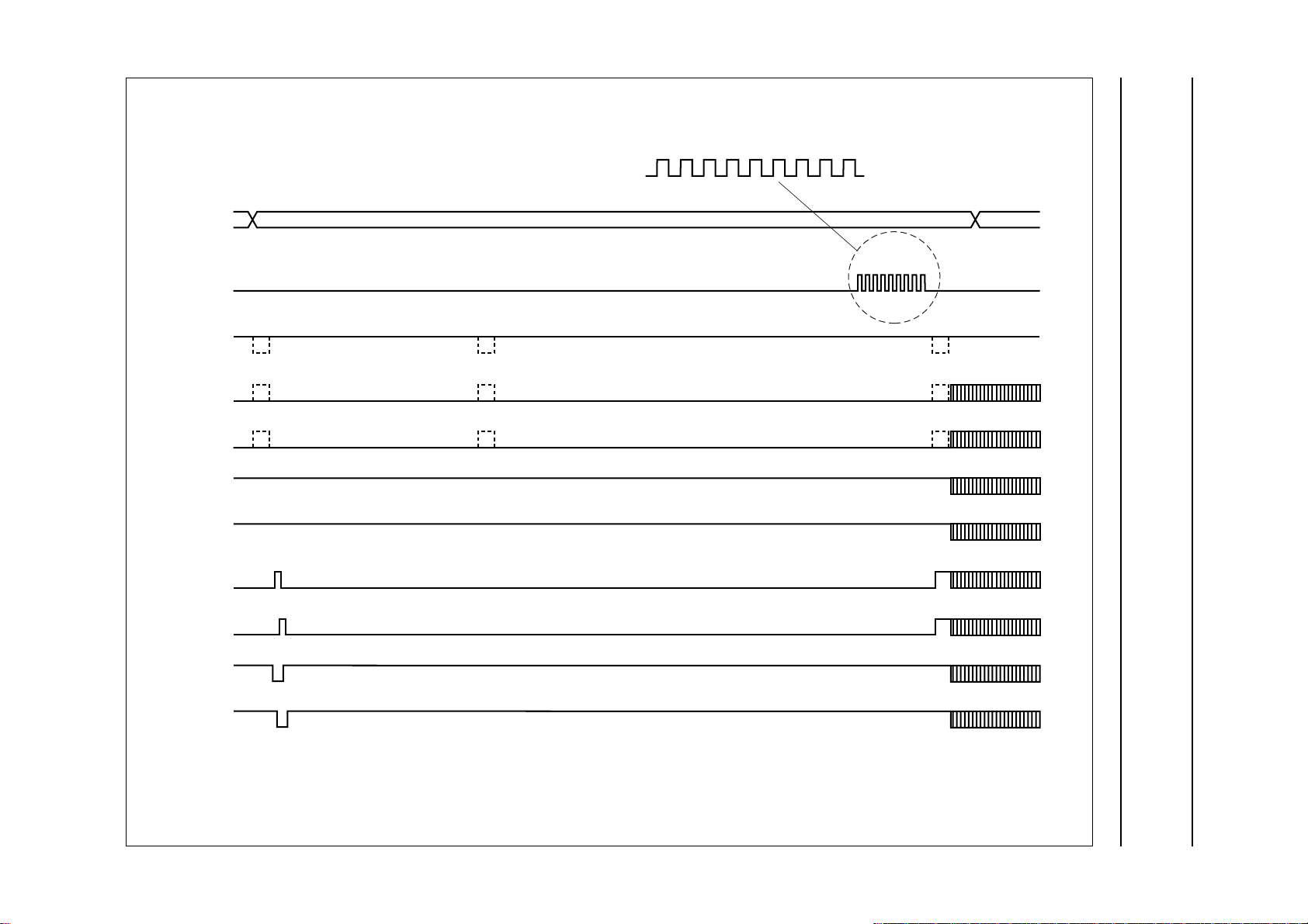
This text is here in white to force landscape pages to be rotated correctly when browsing through the pdf in the Acrobat reader.This text is here in
n
_white to force landscape pages to be rotated correctly when browsing through the pdf in the Acrobat reader.This text is here inThis text is here in
white to force landscape pages to be rotated correctly when browsing through the pdf in the Acrobat reader. white to force landscape pages to be ...
1999 Apr 02 26
dbook, full pagewidth
Philips Semiconductors Product specification
Digital camera USB interface IC SAA8117HL
INE#
HD
SHUTTER
A1
A2
A3
A4
B1
687
691
695
699
703
707
711
715
719
723
727
731
735
739
743
747
751
755
1 2 3
751
755
2
22
779
799
RESET_DATA [9 to 0] + 20RESET_DATA [9 to 0]
2
22
2
22
25
28
RESET_DATA [9 to 0] + 20RESET_DATA [9 to 0]
RESET_DATA [9 to 0] + 20RESET_DATA [9 to 0]
779
779
780
799
799
800
B2
B3
B4
780
27
30
24
29
26
31
800
FCE147
Fig.18 Vertical pulses for VGA sensors (3).
Page 27
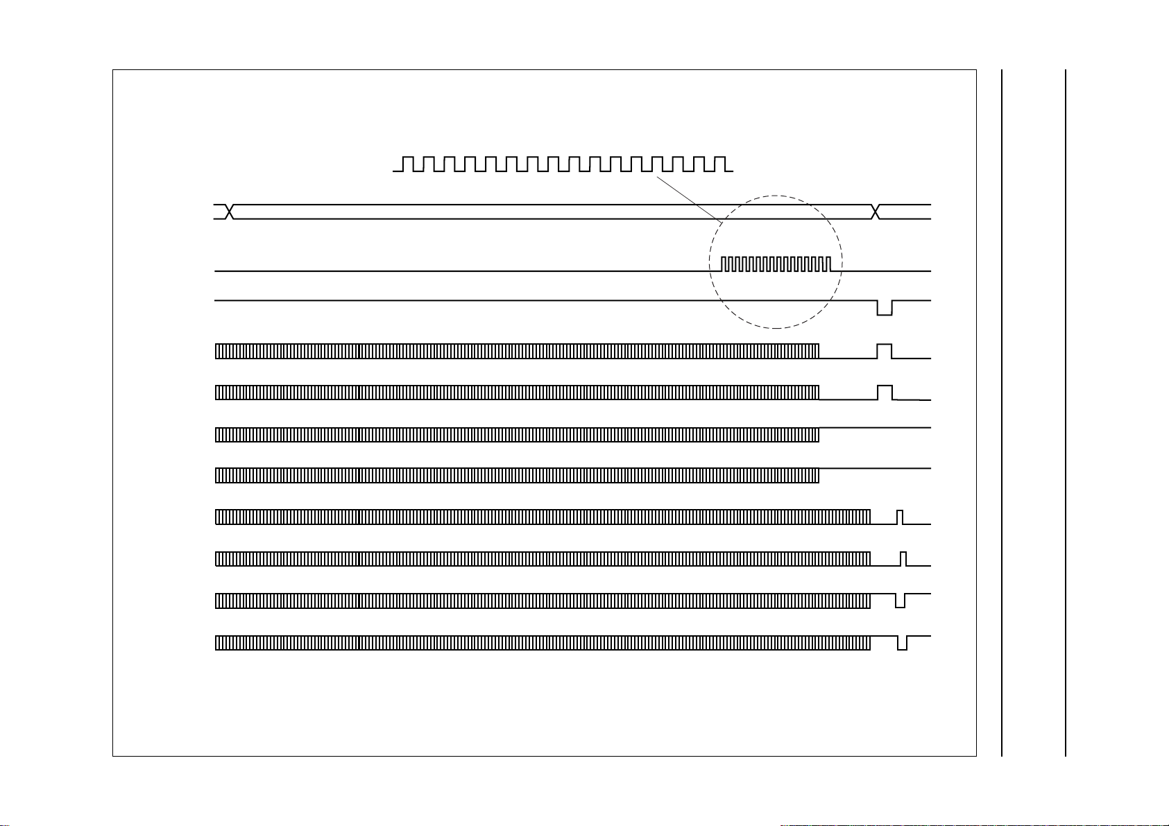
This text is here in white to force landscape pages to be rotated correctly when browsing through the pdf in the Acrobat reader.This text is here in
n
_white to force landscape pages to be rotated correctly when browsing through the pdf in the Acrobat reader.This text is here inThis text is here in
white to force landscape pages to be rotated correctly when browsing through the pdf in the Acrobat reader. white to force landscape pages to be ...
1999 Apr 02 27
631
635
639
643
671
667
663
659
655
651
647
675
679
683
687
dbook, full pagewidth
711
707
703
699
695
691
715
719
723
727
731
735
739
743
747
751
755
Philips Semiconductors Product specification
Digital camera USB interface IC SAA8117HL
INE#
HD
SHUTTER
A1
A2
A3
A4
B1
B2
B3
2 3 4
751
755
2
22
2
22
2
22
25
27
24
28
30
29
B4
Fig.19 Vertical pulses for VGA sensors (4).
26
FCE148
31
Page 28
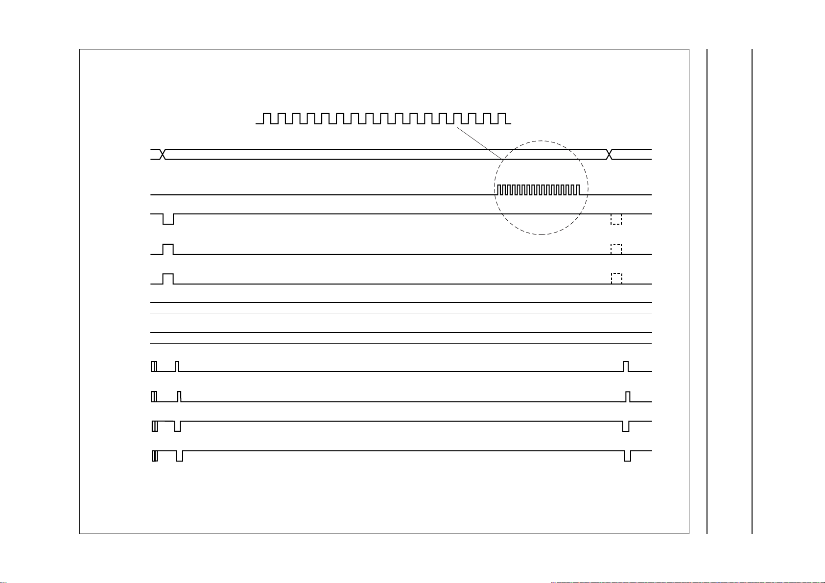
This text is here in white to force landscape pages to be rotated correctly when browsing through the pdf in the Acrobat reader.This text is here in
n
_white to force landscape pages to be rotated correctly when browsing through the pdf in the Acrobat reader.This text is here inThis text is here in
white to force landscape pages to be rotated correctly when browsing through the pdf in the Acrobat reader. white to force landscape pages to be ...
1999 Apr 02 28
623
627
631
635
639
643
647
651
655
659
663
667
671
675
679
683
687
dbook, full pagewidth
711
707
703
699
695
691
715
719
723
727
731
735
739
743
747
751
755
Philips Semiconductors Product specification
Digital camera USB interface IC SAA8117HL
INE#
HD
SHUTTER
A1
A2
A3
A4
B1
B2
B3
3 4 5
751
755
2
22
2
22
2
22
25
28
27
30
24
29
2
22
2
22
2
22
25
27
24
28
30
29
B4
26
26
31
31
FCE149
Fig.20 Vertical pulses for VGA sensors (5).
Page 29
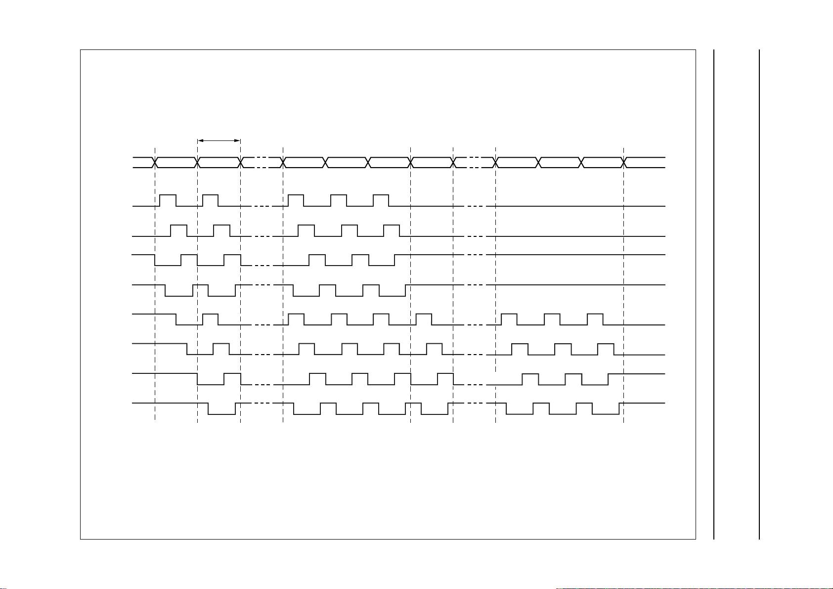
This text is here in white to force landscape pages to be rotated correctly when browsing through the pdf in the Acrobat reader.This text is here in
n
_white to force landscape pages to be rotated correctly when browsing through the pdf in the Acrobat reader.This text is here inThis text is here in
white to force landscape pages to be rotated correctly when browsing through the pdf in the Acrobat reader. white to force landscape pages to be ...
1999 Apr 02 29
1/(6 MHz) = 0.167 µs
INE#
0 1 2 3 490 491 492 493 494 518 519 520 521 522489
A1
A2
A3
A4
dbook, full pagewidth
Philips Semiconductors Product specification
Digital camera USB interface IC SAA8117HL
B1
B2
B3
B4
FCE150
Fig.21 Vertical pulses for VGA sensors (6).
Page 30
Philips Semiconductors Product specification
Digital camera USB interface IC SAA8117HL
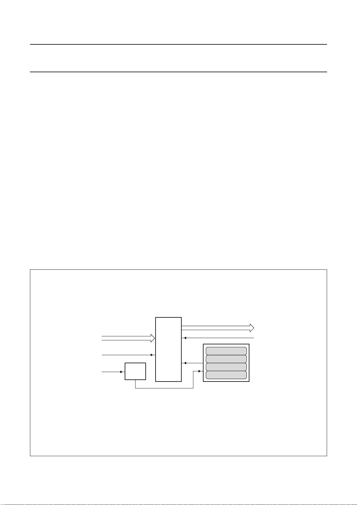
8.8 USB video FIFO
The USB video FIFO is programmed via the I2C-bus
(see Fig.22). The FIFO is designed to achieve three
different packets containing video on the isochronous USB
channel. Video data is contained in a chain of equally sized
USB packets, except for the last packet of a video frame
which is always smaller. The video frames can be
separated from each other by one or more 0-length
packets. For low frame rates (below 10 frames/s) there are
always 0-length packets in the stream. The host can
synchronize on the smaller packets for the high frame
rates and on the 0-length packets for the low frame rates.
For every mode the FIFO must be adjusted. There are
three parameters to program the video FIFO:
2
C_Packet_Size: this value indicates the length of all
• I
packets with video data except for the last packet of a
video frame
• I2C_FIFO_Offset: this value indicates the number of
data in the FIFO before a new packet is transmitted over
the USB
• I2C_Read_Spacing: this value indicates the number of
12 MHz clock cycles between read actions from the
FIFO.
Moreover the FIFO is enabled and disabled with
2
C_Active.
I
The write process to the FIFO is controlled by the transfer
buffer and is not programmable.
The read process is executed in the PSIE-MMU and is
driven by the USB frame interval (1 ms). Every frame
interval the PSIE-MMU tries to read I2C_Packet_Size
bytes from the FIFO. This read process will not be started
when a new video frame is stored in the FIFO and there
are less than I2C_FIFO_Offset bytes written. The read
process stops if the next bytes are of another video frame,
or if the read-pointer overtakes the write-pointer.
I2C_Read_Spacing determines the read rate. Its value can
easily be determined with the formula:
I2C_Read_Spacing
<
12000
---------------------------------------------
2
C_Packet_Size
I
handbook, full pagewidth
data from transfer buffer
write
WRITE
SYNC
Ptr_to_start_Vframe
FIFO
Fig.22 USB video FIFO.
1999 Apr 02 30
data to PSIE-MMU
read
2
C_FIFO_Offset
read
enable
I
2
C_Packet_Size
I
2
I
C_Read_Spacing
2
I
C_Active
FCE151
Page 31
Philips Semiconductors Product specification
Digital camera USB interface IC SAA8117HL
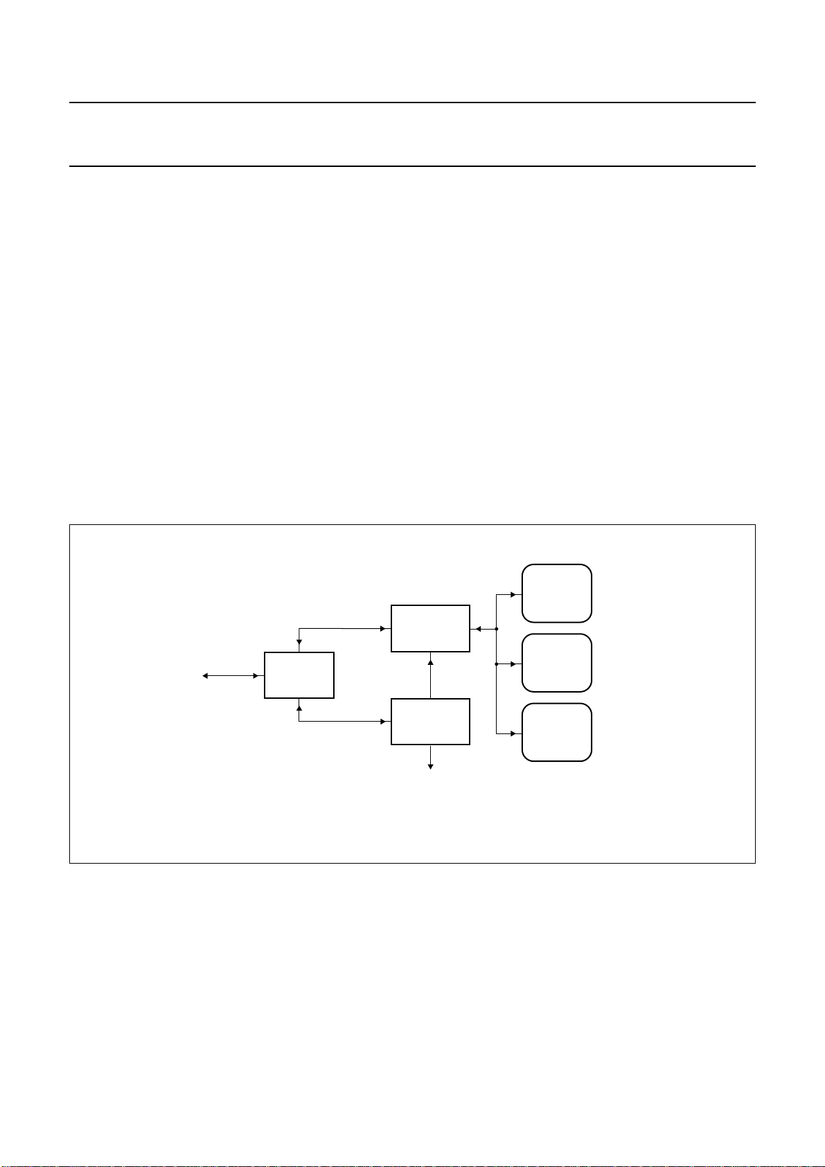
8.9 PSIE-MMU, I2C-bus interface and USB RAM
space
The Programmable Serial Interface Engine (PSIE) and
Memory Management Unit (MMU) is the heart of the USB
protocol hardware (see Fig.23). It formats the actual
packets that are transferred to the USB and passes the
incoming packets to the right end-point buffers. These
buffers are allocated as part of the USB RAM space.
The microcontroller communicates via the I
2
C-bus with the
PSIE-MMU. The I2C-bus protocol distinguishes three
register spaces. These spaces are addressed via different
commands. The command is sent to the command
address. Depending on the command it is sent to the
PSIE-MMU and/or to the command interpreter which
configures the (de-)mux to open the path to the right
register space. Subsequent write/read to/from the data
address store or retrieve data from the register space is
selected by the command.
handbook, full pagewidth
PI_Address + 0X
to/from
microcontroller
I2C-BUS
INTERFACE
8.10 ATX and external ATX interface
The SAA8117HL contains an analog bus driver, called the
ATX. It incorporates a differential and two single-ended
receivers and a differential transmitter. The interface to the
bus consists of a differential data pair (ATXDM and
ATXDP). The SAA8117HL contains also an interface to an
external ATX as backup solution.
PSIE-MMU
REGISTER
SPACE
(DE)MUX
SET MODE
REGISTER
SPACE
COMMAND
PI_Address + 10
INTERPRETER
PSIE-MMU
Fig.23 I2C-bus interface and register map.
1999 Apr 02 31
NON USB
AND
VIDEO FIFO
REGISTERS
to
FCE152
Page 32

Philips Semiconductors Product specification
Digital camera USB interface IC SAA8117HL
8.11 Audio
The PLL converts the 48 MHz to 256fs (fs= audio sample
frequency). There are three modes for the PLL to achieve
the sample frequencies of 48, 44.1 or 32 kHz
(see Table 1).
In the Fixed Gain Amplifier (FGA) the microphone input is
amplified by 20 dB.
The bit stream ADC samples the audio signal. It runs at an
oversample rate of 256 times the base sample rate. In the
application, the bit stream can be converted to parallel
16-bit samples. This conversion is programmable with
respect to the effective sample frequency (dropping
sample results in a lower effective sample frequency) and
sample resolution. As a result the effective sample rate
can be determined.
Table 1 ADC clock frequencies and sample frequencies
CLOCK
(MHz)
8.1920 1 32 4.096
1 1.2996 1 44.1 5.6448
12.2880 1 48 6.144
Note
1. Not supported.
DIVIDING
NUMBER
2 16 2.048
4 8 1.042
8 note 1 note 1
2 22.05 2.8224
4 1 1.025 1.41 12
8 5.5125 0.7056
2 24 3.072
4 12 1.536
8 6 0.768
SAMPLE
FREQUENCY
(kHz)
ADC CLOCK
(MHz)
8.12 Power management
The USB requires the device to switch power states.
The SAA8117HL contains a power management module
since the device may not consume more than 500 µA
during the power state called SUSPEND. This requires
that even the crystal oscillator must be switched off.
The SAA8117HL is also not functional except for some
logic that enables the IC to wake-up the camera. After
wake-up of the SAA8117HL first the clock to the
microcontroller is generated and thereafter an interrupt is
generated to wake-up the controller. Therefore the clock of
the microcontroller is generated by the SAA8117HL.
The power management module also sets a flag in register
2
C_SET_MODE_AND_READ. After a reset the
I
microcontroller should check this register via the I2C-bus
and find the cause of the wake-up. Different causes may
require different start-up routines.
The internal video processing core uses another
V
domain which can be switched during SUSPEND.
DDD
The PPG is switched off by setting SN_Resume and
resetting SN_PAL_VGA. In non CIF modes the power
consumption is reduced by resetting SN_Compress and
SN_CLK_Compress_On.
The SAA8117HL has the feature to independently
wake-up from SUSPEND, but requires a signal from the
microcontroller before going into SUSPEND (via the signal
on pin SUSREADYNOT).
Since the main oscillator of the SAA8117HL is switched off
during SUSPEND precautions are needed to avoid
undefined states when the clock is switched on. This is
ensured via the pins CLOCKON and TRC.
Pin CLOCKON goes HIGH as soon as the main oscillator
is switched on. The oscillator will need some time to make
a stable 48 MHz signal. However, the clock is only passed
through to other parts of the SAA8117HL when the level on
pin TRC reaches a certain threshold. The time needed to
reach the threshold can be trimmed with an RC-circuit.
1999 Apr 02 32
Page 33

Philips Semiconductors Product specification
Digital camera USB interface IC SAA8117HL
9 CONTROL REGISTER DESCRIPTION
This Chapter gives an overview of all registers.
9.1 SNERT (UART)
The following registers are accessible via SNERT (see Table 2).
Table 2 SNERT write registers of the SAA8117HL
ADDRESS NAME FUNCTION FORMAT
C0 − reserved −
C1 − reserved −
C2 CONTROL17_0 various control bits see Table 3
C3 CONTROL17_1 various control bits see Table 5
C4 VP_SQCIF_OFFSET vertical (MSN) and horizontal (LSN) offset for sub-QCIF
mode
C5 CONTROL17_2 various control bits see Table 6
C6 PPG_SHUTTERSPEED_0 bits of shutter speed 0 see Table 8
C7 PPG_SHUTTERSPEED_1 bits of shutter speed 1 see Table 9
C8 PPG_CLPOB_START_LSB LSB start position control for CLPOB pulse byte
C9 PPG_CLPOB_STOP_LSB LSB stop position control for CLPOB pulse byte
CA PPG_CLPDM_START_LSB LSB start position control for CLPDM pulse byte
CB PPG_CLPDM_STOP_LSB LSB stop position control for CLPDM pulse byte
CC CLPMSB MSBs of CLPOB_Start, CLPOB_Stop, CLPDM_Start and
CLPDM_Stop
nibble
see Table 10
1999 Apr 02 33
Page 34
Philips Semiconductors Product specification
Digital camera USB interface IC SAA8117HL
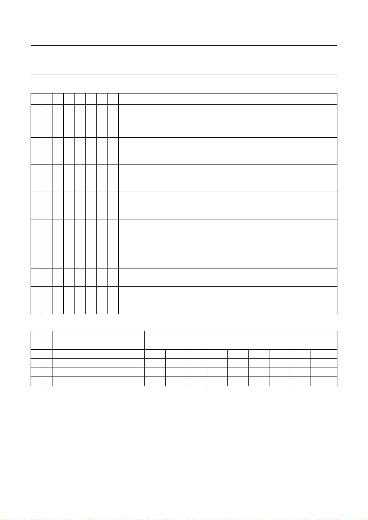
Table 3 Detailed description of SNERT register CONTROL17_0 (address 0xC2)
76543210 PARAMETER
EIRRAH
X exchanges the chrominance irregularities when needed; toggle the bit to ensure
timing of chrominance signal; the value must be determined experimentally (can
be different for different modes)
Snapshot
1 transported in 4:2:2 format
0 transported in 4:2:0 format
Inband_Control
1 in band synchronization words are inserted in the video data stream
0 only active video data is transmitted over USB
Compression_Ratio
1 ratio is 4 times
0 ratio is 3 times
Compress
1 compression is active; only to be used in case (for this register) bit 2 = 1 and
bit 1 = 0 since compression functions are for CIF only; CIF format must be
compressed unless the frame rate is 3.75 Hz
0 compression module is switched off and power consumption is minimized for this
module
Output_Format_Select
X X see Table 4
P AL_VGA
1 PAL sensor
0 VGA sensor
Table 4 Detailed description of bit 2 and bit 1 of SNERT register CONTROL17_0
21
0 0 sub-QCIF 24 20 15 12 10 7.5 5 3.75 −
0 1 QCIF 24 20 15 12 10 7.5 5 3.75 −
1 0 CIF −−15 12 10 7.5 5 3.75 −
1 1 VGA; note 1 −−−−−−−−0.9375
Note
1. Only valid when a VGA sensor is applied. The VGA output is not compressed.
1999 Apr 02 34
OUTPUT_FORMAT_SELECT
PARAMETER
FRAME RATE WITH RESPECT TO OUTPUT FORMAT
Page 35
Philips Semiconductors Product specification
Digital camera USB interface IC SAA8117HL
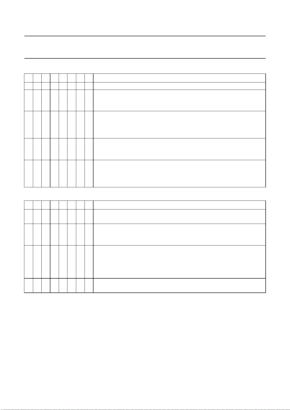
Table 5 Detailed description of SNERT register CONTROL17_1 (address 0xC3)
76543210 PARAMETER
XXXX reserved
CLK_Compress_On
1 compression clock active
0 compression module is brought to low power state
Prefilter B_Comb
1 horizontal scaling factor exceeds 3 (only functioning if bit 1 is also set to logic 1);
this bit switches prefilter B to 13 taps
0 prefilter B is as described for bit 1
Prefilter B_On/Off
1 horizontal scaling factor exceeds 2; the prefilter with 7 taps is switched on
0 prefilter B is bypassed
Prefilter A_On/Off
1 prefilter A with 3 taps is on; must be set to logic 1 when bit 2 is set to logic 1 to
obtain the overall wanted frequency response
0 prefilter A is bypassed
Table 6 Detailed description of SNERT register CONTROL17_2 (address 0xC5)
76543210 PARAMETER
PIX_nr0 to PIX_nr2
X X X 3 LSBs of 10 bits pixel number for autoexposure control (7 LSBs in register 0xC6)
Shutter_Update_Buffer
1 update of the shutter speed is buffered
0 no buffering (immediately destroying of the current video frame)
Resume
1 video processing and PPG are switched of; if a VGA sensor is selected the vertical
transport pulses are not switched off but this must be done by selecting a PAL
sensor (register 0xC2 bit 0)
0 PGG pulses generated
PPG_Mode_Frame_Rate
X X X see Table 7
1999 Apr 02 35
Page 36
Philips Semiconductors Product specification
Digital camera USB interface IC SAA8117HL
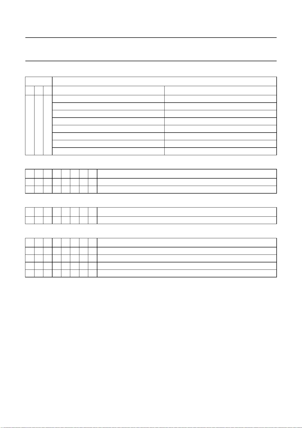
Table 7 Detailed description of bit 2 to bit 0 of SNERT register CONTROL17_2
BIT PARAMETER OF PPG_MODE_FRAME_RATE
2 1 0 VGA PAL
0 0 0 24 24
0 0 1 20 20
0 1 0 15 15
0 1 1 10 12
1 0 0 7.5 10
101 5 7.5
1 1 0 3.75 5
1 1 1 0.9375 3.75
Table 8 Detailed description of SNERT register PPG_SHUTTERSPEED_0 (address 0xC6)
76543210 PARAMETER
X 1 LSB of 9-bit line number (8 MSBs in register 0xC7)
XXXXXXX7MSBs of 10-bit pixel number (3 LSBs in register 0xC5)
Table 9 Detailed description of SNERT register PPG_SHUTTERSPEED_1 (address 0xC7)
76543210 PARAMETER
XXXXXXXX8MSBs of 9-bit line number (LSB in register 0xC6)
Table 10 Detailed description of SNERT register CLPMSB (address0xCC)
76543210 PARAMETER
X X 2 MSBs of CLPOB_Start (LSBs in register 0xC8)
X X 2 MSBs of CLPOB_Stop (LSBs in register 0xC9)
X X 2 MSBs of CLPDM_Start (LSBs in register 0xCA)
X X 2 MSBs of CLPDM_Stop (LSBs in register 0xCB)
1999 Apr 02 36
Page 37
Philips Semiconductors Product specification
Digital camera USB interface IC SAA8117HL
9.2 I2C-bus interface
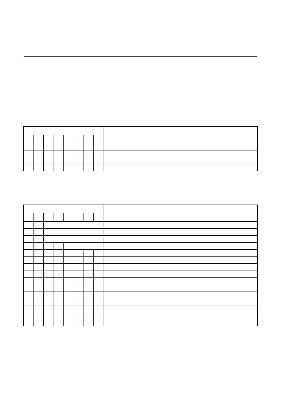
The I2C-bus interface uses two addresses:
• Command address for writing commands to the Memory Manager (MM)
• Data address for writing/reading data to/from the Memory Manager (MM).
The 6 MSBs of the two addresses are equal and are defined by the PI_address = 010111 (see Table 11). The LSBs of
the addresses differentiate between the command address and the data address. When bit 1 is logic 1 the address is
the command address (0x5E) and when bit 1 is logic 0 the address is one of the data addresses (0x5C or 0x5D).
2
Table 11 I
C-bus addresses
BIT
ADDRESS
76543210
010111000x5C: for writing data to the memory manager
010111010x5D: for reading data from the memory manager
010111100x5E: for writing commands
010111110x5F: not in use
9.2.1 C
OMMANDS
The commands listed in Table 12 must be sent to the I2C-bus address 0x5E.
Table 12 I
2
C-bus USB command codes
BIT
FUNCTION
76543210
0 0 end-point number select end-point
0 1 end-point number read/write status
1 0 end-point number initialize/read status information
1101 address read/write register bank
11100XXXnot used
11101000set non-USB register
11110000read/write data
11110001acknowledge setup
11110010set buffer empty
11111010set buffer full
11110100read interrupt register
11110101read current frame number
11110110send resume
11110111set status change bits
11110011set mode
1999 Apr 02 37
Page 38

Philips Semiconductors Product specification
Digital camera USB interface IC SAA8117HL
Table 13 Set mode and write register overview
BYTE SET MODE AND WRITE
1 N1 timer; programmable timer for power management; counts 12 MHz cycles; must be bigger than number
of cycles needed for the microcontroller to go in power-down state after pin SUSREADYNOT is made LOW
2 N2 timer; programmable timer for power management; counts 12 MHz cycles; determines the time between
when the microcontroller clock is switched off and the main clock is switched off
3 PSIE-MMU control byte (see Table 14)
Table 14 Detailed description of PSIE-MMU control byte (byte 3)
76543210 PARAMETER
X X X reserved
interrupt after isochronous audio transfer
1 for each isochronous audio transfer an interrupt to the microcontroller will
be generated; default set to logic 1 upon general Power-on reset and/or
bus reset by the SAA8117HL
0 no interrupts are given to the microcontroller
interrupt after isochronous video transfer
1 for each isochronous video transfer an interrupt to the microcontroller will
be generated; default set to logic 1 upon general Power-on reset and/or
bus reset by the SAA8117HL
0 no interrupts are given to the microcontroller
audio end-point
1 audio end-point enabled; default set to logic 1 upon general Power-on reset
and/or bus reset by the SAA8117HL
0 audio end-point disabled; the PSIE-MMU will not react on in-tokens on the
audio end-point
video end-point
1 video end-point enabled; default set to logic 1 upon general Power-on reset
and/or bus reset by the SAA8117HL
0 video end-point disabled; the PSIE-MMU will not react on in-tokens on the
video end-point
error debug mode
1 interrupts are generated only in the event that the transfer is not
successfully completed; the microcontroller can read data from the interrupt
and status registers to see the cause of this error
0 all successful USB transactions are reported to the microcontroller via an
interrupt; default set to logic 0 upon general Power-on reset by the
SAA8117HL
1999 Apr 02 38
Page 39
Philips Semiconductors Product specification
Digital camera USB interface IC SAA8117HL
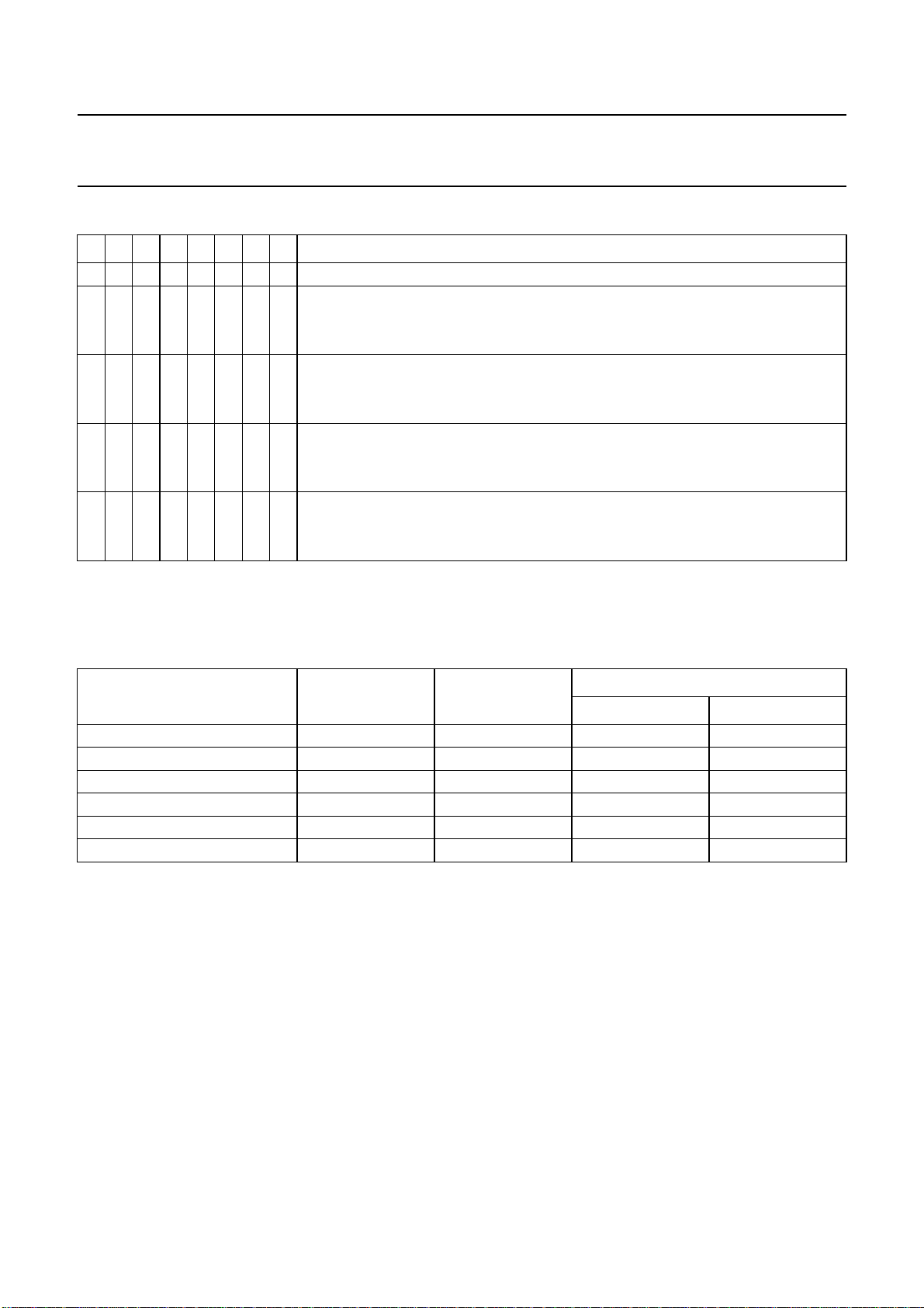
Table 15 Detailed description of PSI-MMU set mode and status byte
76543210 PARAMETER
XXXX reserved
remote wake-up status flag
1 remote wake-up when device is in SUSPEND mode
0 no remote wake-up
resume status flag
1 bus resume by the host when device is in SUSPEND mode
0 no bus resume
bus reset status flag
1 bus reset
0 no bus reset
power-up status flag
1 general power up reset
0 no power up reset
9.2.2 E
The SAA8117HL has 6 logical end-points which are listed in Table 16.
Table 16 Mapping of logic to physical end-point numbers for used end-points
Control end-point 0801
Control end-point 1823
Interrupt end-point 2 8 − 4
Interrupt end-point 3 8 − 5
Iso video end-point 4 96.0 − 6
Iso video end-point 5 35.1 − 7
ND-POINTS
END-POINT NAME
LOGIC
END-POINT
BUFFER SIZE
PHYSICAL END-POINT
OUT IN
1999 Apr 02 39
Page 40
Philips Semiconductors Product specification
Digital camera USB interface IC SAA8117HL
9.2.3 CONTROL TOP REGISTERS
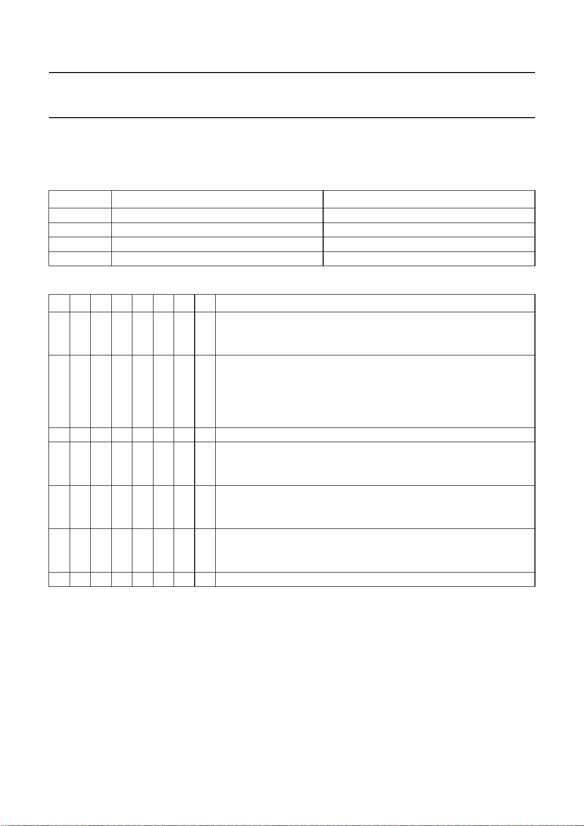
The following registers can be written on I2C-bus address 1 after the command 0xE8 on I2C-bus address 0.
2
Table 17 I
ADDRESS NAME FUNCTION
0x08 CLKSHOP CONTROL clock control
0x09 RSTGEN AND_PLL CONTROL reset control
0x0A I/O MUX CONTROL mux block control
0x0B POWER CONTROL ANALOG MODULES power-on analog modules control
Table 18 Detailed description of I
76543210 PARAMETER
1 sel_ad: clock generated from ADC
0 sel_pll: clock generated from PLL
C-bus control top registers (base address 0x08)
2
C-bus control top register CLKSHOP CONTROL (address 0x08)
select ADC clock source
set clock dividers for ADC
0 0 set_divide00: divided by 1
0 1 set_divide01: divided by 2
1 0 set_divide10: divided by 4
1 1 set_divide11: divided by 8
X reserved
disable 48 MHz clock
1 dis_clk_48: disable 48 MHz clock
0 enable clock
disable receiver clock
1 dis_clk_rec: disable receiver clock
0 enable clock
disable ADC clock
1 dis_clk_ad: disable ADC clock
0 enable clock
X reserved
1999 Apr 02 40
Page 41
Philips Semiconductors Product specification
Digital camera USB interface IC SAA8117HL
Table 19 Detailed description of I2C-bus control top register RSTGEN AND PLL CONTROL (address 0x09)
76543210 PARAMETER
set PLL frequency
0 0 fcode00: 256 × 44.1 kHz
0 1 fcode01: 256 × 32 kHz
1 0 fcode10: 256 × 48 kHz
1 1 fcode11: 256 × 44.1 kHz
X X reserved
reset PSIE-MMU top module
1 upc_rst_mmu: resetting the USB protocol block (called PSIE-MMU) during
tests or in the event of errors
0 no reset
X reserved
reset ADIF top module
1 upc_rst_adif: resetting the digital audio part during tests or in the event of
errors
0 no reset
reset AGC module
1 upc_rst_AGC: resetting the AGC control during tests or in the event of
errors
0 no reset
2
Table 20 Detailed description of I
76543210 PARAMETER
XXXXXXXXreserved
C-bus control top register I/O MUX CONTROL (address 0x0A)
1999 Apr 02 41
Page 42

Philips Semiconductors Product specification
Digital camera USB interface IC SAA8117HL
Table 21 Detailed description of I2C-bus control top register POWER CONTROL OF ANALOG MODULES
(address 0x0B)
76543210 PARAMETER
X X reserved
power control PLL module
1 upc_pll_off: PLL power off
0 power on
X reserved
power control ADC module left channel
1 upc_adl_off: power off
0 power on
power control ADC module right channel
1 upc_adr_off: power off
0 power on
power control AGC module left channel
1 upc_AGCl_off: power off
0 power on
power control AGC module right channel
1 upc_AGCr_off: power off
0 power on
1999 Apr 02 42
Page 43
Philips Semiconductors Product specification
Digital camera USB interface IC SAA8117HL
9.2.4 VIDEO FIFO REGISTERS
Table 22 Overview of I2C-bus video FIFO registers (base address 0x04)
ADDRESS NAME FUNCTION
0x04 FIFO OFFSET 8 LSBs of the offset value
0x05 FIFO ACTIVE AND FIFI OFFSET FIFO active and 3 MSBs of the offset value
0x06 PACKET SIZE 8 LSBs of packet size value
0x07 READ SPACING AND PACKET SIZE read spacing and 2 MSBs of packet size value
2
Table 23 Detailed description of I
76543210 PARAMETER
XXXXXXXX mode_fifo_offset: sets the minimum contents of the FIFO that has to be
C-bus video FIFO register FIFO OFFSET (address0x04)
FIFO offset
reached, before a new video frame will be put on the USB bus. This value
can be set between 0 and 2047. Total of 11 bits with 8 LSBs in this register
and 3 MSBs in register 0x05.
Table 24 Detailed description of I
2
C-bus video FIFO register FIFO ACTIVE AND FIFI OFFSET (address 0x05)
76543210 PARAMETER
FIFO active
1 mode_active: FIFO is active and the contents of the other mode registers
should not be updated by the microcontroller (maledictive)
0 FIFO not active
XXXX reserved
FIFO offset
X X X 3 MSBs of the offset value; see also register 0x04
2
Table 25 Detailed description of I
C-bus video FIFO register PACKET SIZE (address 0x06)
76543210 PARAMETER
packet size
XXXXXXXX mode_packet_size: sets the packet size of the USB video channel. Packets
can vary in size between 0 and 1023. Total of 10 bits with 8 LSBs in this
register and 2 MSBs in register 0x07.
2
Table 26 Detailed description of I
C-bus video FIFO register READ SPACING AND PACKET SIZE (address 0x07)
76543210 PARAMETER
read spacing
XXXXXX mode_read_spacing: sets the periodicity of the read pulses; the periodicity
can be set from 1 to 63 (from ‘000001’ to ‘111111’)
packet size
X X mode_packet_size: 2 MSBs of the value (8 LSBs in register 0x06)
1999 Apr 02 43
Page 44

Philips Semiconductors Product specification
Digital camera USB interface IC SAA8117HL
9.2.5 ADIF TOP REGISTERS
Table 27 Overview of I2C-bus ADIF top registers (base address 0x0C)
ADDRESS NAME FUNCTION
0x0C AGC CONTROL GENERAL AGC control general
0x0D AGC CONTROL GAIN LEFT AGC control gain left
0x0E AGC CONTROL GAIN RIGHT AGC control gain right
0x0F ADIF CONTROL I
2
Table 28 Detailed description of I
C-bus ADIF top register ADIF CONTROL (address 0x0F)
76543210 PARAMETER
X reserved
number of bytes per sample
0 0 0 (reserved)
0 1 1 (8 bits audio samples)
1 0 2 (16 bits audio samples)
1 1 3 (24 bits audio samples)
selection mono/stereo operation
0 mono
1 stereo
selection input for ADC path (ADIF mux)
0 digital input (from I
1 analog input (from Vin_left and Vin_right)
selection high-pass filter (DC filter) for ADC down-sample filter
0 high-pass filter off
1 high-pass filter on
selection UDAI serial input format
00 I
2
S-bus
0 1 LSB justified, 16 bits
1 0 LSB justified, 18 bits
1 1 LSB justified, 20 bits
2
S-bus input and ADIF2MMU
2
S-bus)
1999 Apr 02 44
Page 45
Philips Semiconductors Product specification
Digital camera USB interface IC SAA8117HL
10 LIMITING VALUES
In accordance with the Absolute Maximum Rating System (IEC 134).
SYMBOL PARAMETER CONDITIONS MIN. MAX. UNIT
V
DDA
V
DDD
V
n
T
stg
T
amb
T
j
Note
1. 5 V tolerant buffers.
analog supply voltage −0.5 +4.0 V
digital supply voltage −0.5 +4.0 V
voltage on
pins AGND and DGND −0.5 +4.0 V
pins SCL and SDA note 1 −0.5 +5.5 V
all other pins −0.5 V
+ 0.5 V
DD
storage temperature − 55 +150 °C
operating ambient temperature 0 70 °C
junction temperature −40 +125 °C
11 THERMAL CHARACTERISTICS
SYMBOL PARAMETER CONDITIONS VALUE UNIT
R
th(j-a)
thermal resistance from junction to ambient in free air 51 K/W
1999 Apr 02 45
Page 46
Philips Semiconductors Product specification
Digital camera USB interface IC SAA8117HL
12 CHARACTERISTICS
V
DDD=VDDA
SYMBOL PARAMETER CONDITIONS MIN. TYP. MAX. UNIT
Supplies
V
DDD
V
DDA
V
DGND
V
AGND
I
DDD
I
DDA
T
amb
Inputs
D
ATA AND CONTROL INPUTS: PINS M0 TO M2, YUV0 TO YUV7, LLC, HREF, VSYNC, RESET, GENPOR, ATXCTRL,
RCV, VM0 AND VP0
V
IL
V
IH
Outputs
= 3.3 V ±10%; T
=0to70°C.
amb
digital supply voltage 3.0 3.3 3.6 V
analog supply voltage 3.0 3.3 3.6 V
voltage on pins DGND 0 0 0 V
voltage on pins AGND 0 0 0 V
digital supply current T
analog supply current T
=25°C − 70 − mA
amb
=25°C − 20 − mA
amb
operating ambient temperature 0 25 70 °C
LOW-level input voltage −−0.8 V
HIGH-level input voltage 2 −− V
D
ATA AND CONTROL OUTPUTS: PINS CLK2, SMP, SPEED, SUSPEND, VM, VP AND OEBAR
V
OL
V
OH
LOW-level output voltage −−0.1V
HIGH-level output voltage 0.85V
DDD
CONTROL OUTPUTS: PINS RG, SHUTTER, C1 TO C3, CLK1, SHP AND SHD
V
OL
V
OH
LOW-level output voltage −−0.8 V
HIGH-level output voltage 2.0 −− V
CONTROL OUTPUTS: PINS A1 TO A4 AND B1 TO B4
V
OL
V
OH
LOW-level output voltage −−0.8 V
HIGH-level output voltage 2.6 −− V
CONTROL OUTPUTS: PINS CLPDM AND CLPOB
V
OL
V
OH
LOW-level output voltage −−0.6 V
HIGH-level output voltage 2.2 −− V
Interfaces
2
I
S-BUS: PINS DA, BCK AND WS
V
IL
V
IH
2
I
C-BUS AND SNERT BUS: PINS SDA, SCL, SNDA, SNCL AND SNRES
V
IL
V
IH
V
OL
V
OH
LOW-level input voltage −−0.3V
HIGH-level input voltage 0.7V
DDD
LOW-level input voltage −−0.7 V
HIGH-level input voltage 0.2V
+ 0.9 − V
DDD
LOW-level output voltage note 1 −−0.4 V
HIGH-level output voltage note 1 V
− 0.7 −− V
DDD
DDD
V
−− V
DDD
V
−− V
+ 0.5 V
DDD
1999 Apr 02 46
Page 47
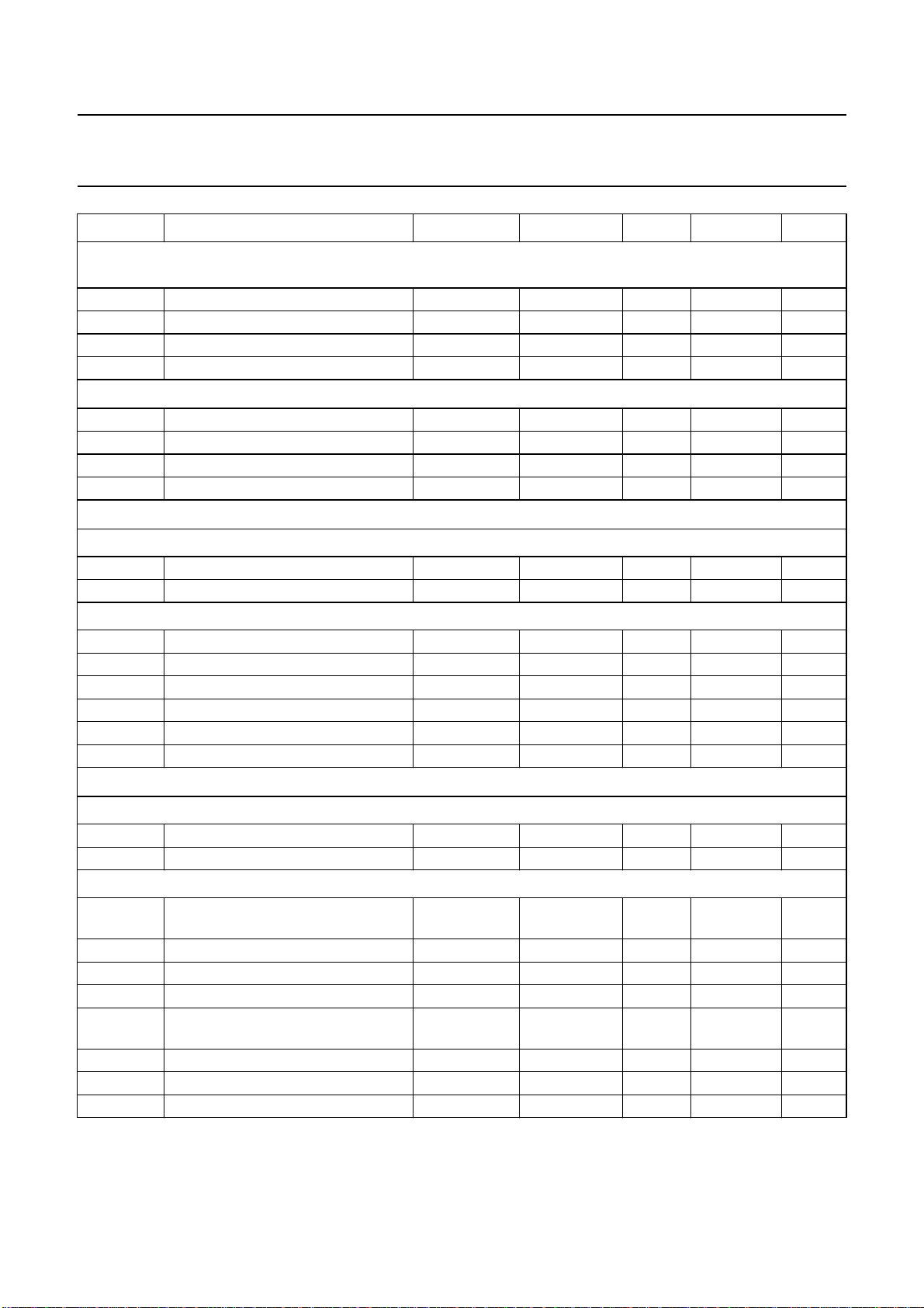
Philips Semiconductors Product specification
Digital camera USB interface IC SAA8117HL
SYMBOL PARAMETER CONDITIONS MIN. TYP. MAX. UNIT
MICROCONTROLLER INTERFACE: PINS SUSREADYNOT, UCPOR, UCINT, CLOCK, CLOCKON, TRC, SNAPSHOT
AND DCDCON
V
IL
V
IH
V
OL
V
OH
Audio Phase-Locked Loop (PLL)
f
i
f
o
B bandwidth − 2.3 − kHz
ζ damping − 0.98 −
∑∆ convertor
I
NPUTS
f
i
V
i(rms)
TRANSFER FUNCTION
N order of the ∑∆ − 3 −
N
bit
N
eqbit
DR
i
f
clk
δ clock frequency duty factor − 50 − %
LOW-level input voltage note 2 −−0.7 V
HIGH-level input voltage note 2 0.2V
+ 0.9 − V
DDD
DDD
+ 0.5 V
LOW-level output voltage note 3 −−0.4 V
HIGH-level output voltage note 3 V
− 0.7 −− V
DDD
clock input frequency − 48 − MHz
clock output frequency note 4 − 11.2996 − MHz
input signal frequency 1 − 20 kHz
input voltage (RMS value) − 800 − mV
number of output bits − 1 −
equivalent output resolution (bit) − 16 −
dynamic range at input note 5 − 96.6 − dB
clock frequency −−5.6448 MHz
Fixed Gain Amplifier (FGA)
LOAD
R
L
C
L
load resistance 5 −− kΩ
load capacitance −−15 pF
TRANSFER FUNCTION
V
i(nom)(p-p)
nominal input voltage
− 226.3 − mV
(peak-to-peak value)
A1 amplification − 20 − dB
V
o(nom)(rms)
nominal output voltage (RMS value) − 800 − mV
S/N signal-to-noise ratio note 6 − 60 − dB
THD total harmonic distortion at HIGH-level;
−−65 − dB
note 7
R
i
R
o
f
i
input impedance 3.35 4.7 6.0 kΩ
output impedance −−100 Ω
input frequency ±3 dB range 100 − 20000 Hz
1999 Apr 02 47
Page 48
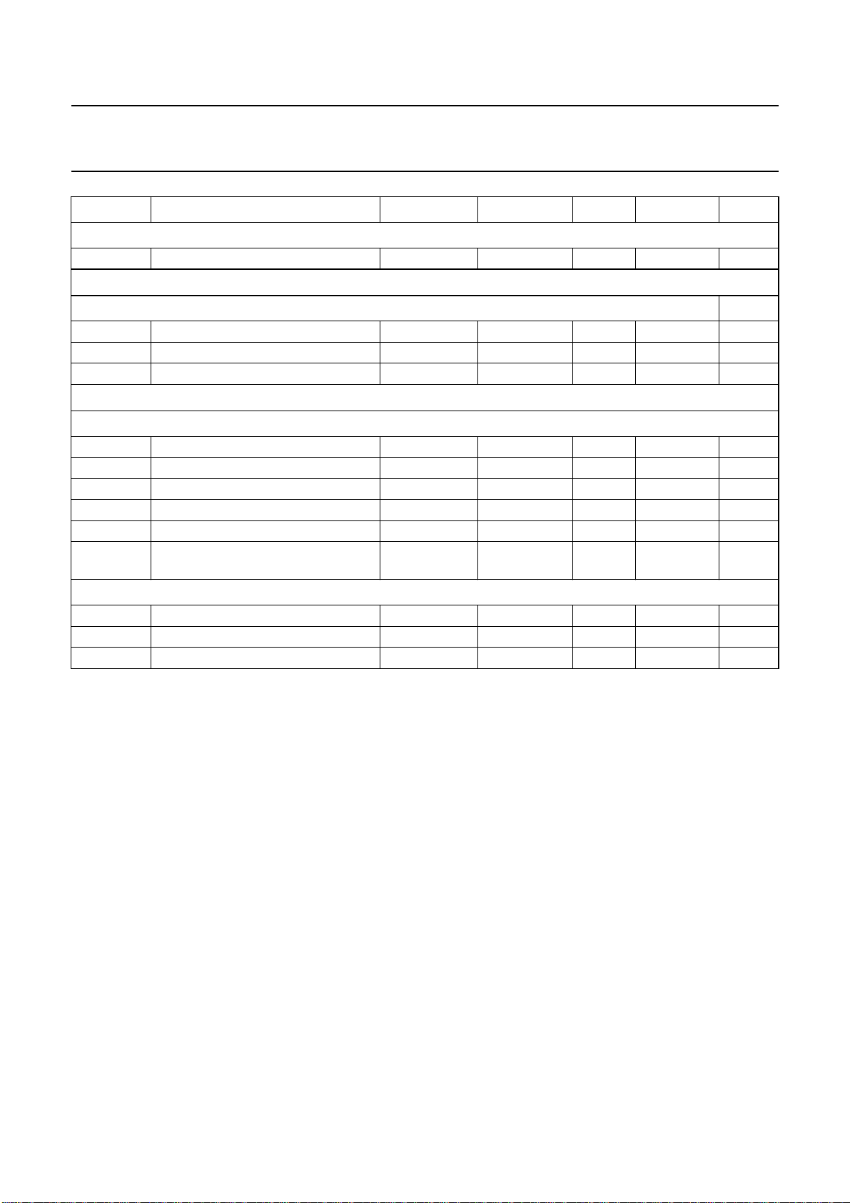
Philips Semiconductors Product specification
Digital camera USB interface IC SAA8117HL
SYMBOL PARAMETER CONDITIONS MIN. TYP. MAX. UNIT
B
IASING
I
ref
FGA/∑∆ path
T
RANSFER FUNCTION
A1 amplification − 20 − dB
S/N signal-to-noise ratio 51 60 70 dB
THD total harmonic distortion −70 −66 −61 dB
ATX transceiver
D
RIVER CHARACTERISTICS IN FULL SPEED MODE: PINS ATXDPAND ATXDM
f
o(sample)
t
t(rise)
t
t(fall)
t
t(match)
V
o(cr)
Z
o
RECEIVER CHARACTERISTICS IN FULL SPEED MODE: PINS ATXDPAND ATXDM
f
s
f
i(D)
t
frame
Notes
1. This applies the outputs: pins SDA and SNDA.
2. This applies the inputs: pins SUSREADYNOT, TRC and SNAPSHOT.
3. This applies the outputs: pins CLOCK, UCINT, UCPOR, CLOCKON and DCDCON.
4. Frequencies depend on PLL settings (see Table 1).
reference current − 25 −µA
audio sample output frequency 4 − 48 MHz
rise transition time CL=50pF 4 − 20 ns
fall transition time CL=50pF 4 − 20 ns
transition time matching note 8 90 − 110 %
output signal crossover voltage 1.3 − 2.0 V
driver output impedance steady state
30 − 42 Ω
drive
audio sample input frequency 5 − 55 kHz
data input frequency rate − 12.00 − Mbits/s
frame interval − 1.000 − ms
V
5. Defined here as: where V
20
------------------log×
V
n(i)(eq)
i
= input voltage and V
i
n(i)(eq)
6. The noise is measured with A-weighting at the nominal input voltage.
7. The distortion is measured at a maximum output voltage of 2.4 V (p-p).
t
8. Transition time matching:
t
t(match)
=
t(rise)
-------------
t
t(fall)
1999 Apr 02 48
= equivalent input noise voltage.
Page 49
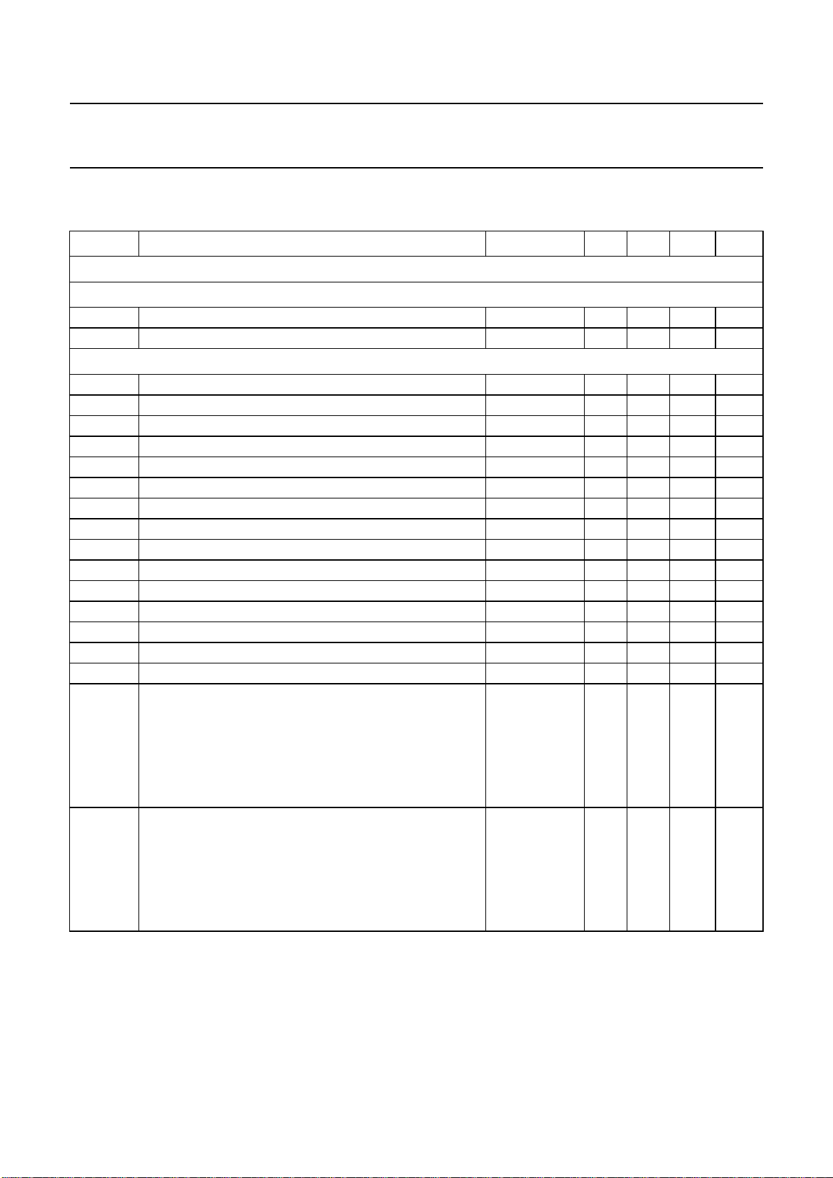
Philips Semiconductors Product specification
Digital camera USB interface IC SAA8117HL
13 TIMING
V
DDD=VDDA
SYMBOL PARAMETER CONDITIONS MIN. TYP. MAX. UNIT
Data input related to LCC (see Fig.24)
Pins YUV0 toYUV7, HREF and VSYNC
t
su(i)(D)
t
h(i)(D)
PPG high-speed pulses for PAL medium resolution sensors; mode 0 (see Fig.25)
t
d1
t
d2
t
d3
t
d4
t
d5
t
d6
t
d7
t
d8
t
WH(C1)
t
WL(C2)
t
WL(SHP)
t
WL(SHD)
t
WL(RG)
t
WL(CLK1)
t
WH(CLK2)
t
r
t
f
= 3.3 V ±10%; load capacitance = 10 pF; T
= 0 to 70 °C; unless otherwise specified.
amb
data input set-up time 1 −− ns
data input hold time 1 −− ns
delay between falling edge C2 and rising edge C1 −2 −1.5 0 ns
delay between rising edge C2 and falling edge C1 1 1.5 2 ns
delay between falling edge C1 and rising edge SHP −3 −1.5 −1ns
delay between rising edge C1 and rising edge SHD −0.5 0 +0.5 ns
delay between rising edge C1 and falling edge RG 0.5 1 2 ns
delay between falling edge CLK1 and rising edge C1 0 1 2 ns
delay between rising edge CLK1 and falling edge C1 −0.5 0 +0.5 ns
delay between rising edge CLK2 and rising edge C1 −2 0 +2 ns
C1 pulse width HIGH 164 165 − ns
C2 pulse width LOW 166 167 − ns
SHP pulse width LOW 81 82 − ns
SHD pulse width LOW 81 82 − ns
RG pulse width LOW 83 84 − ns
CLK1 pulse width LOW 164 165 − ns
CLK2 pulse width HIGH 79 80 − ns
rise time note 1
pulse C1 − 4.5 − ns
pulse C2 − 4 − ns
pulse RG − 4 − ns
pulse SHP − 4 − ns
pulse SHD − 4 − ns
fall time note 1
pulse C1 − 4 − ns
pulse C2 − 4 − ns
pulse RG − 4 − ns
pulse SHP − 4.5 − ns
pulse SHD − 4.5 − ns
1999 Apr 02 49
Page 50
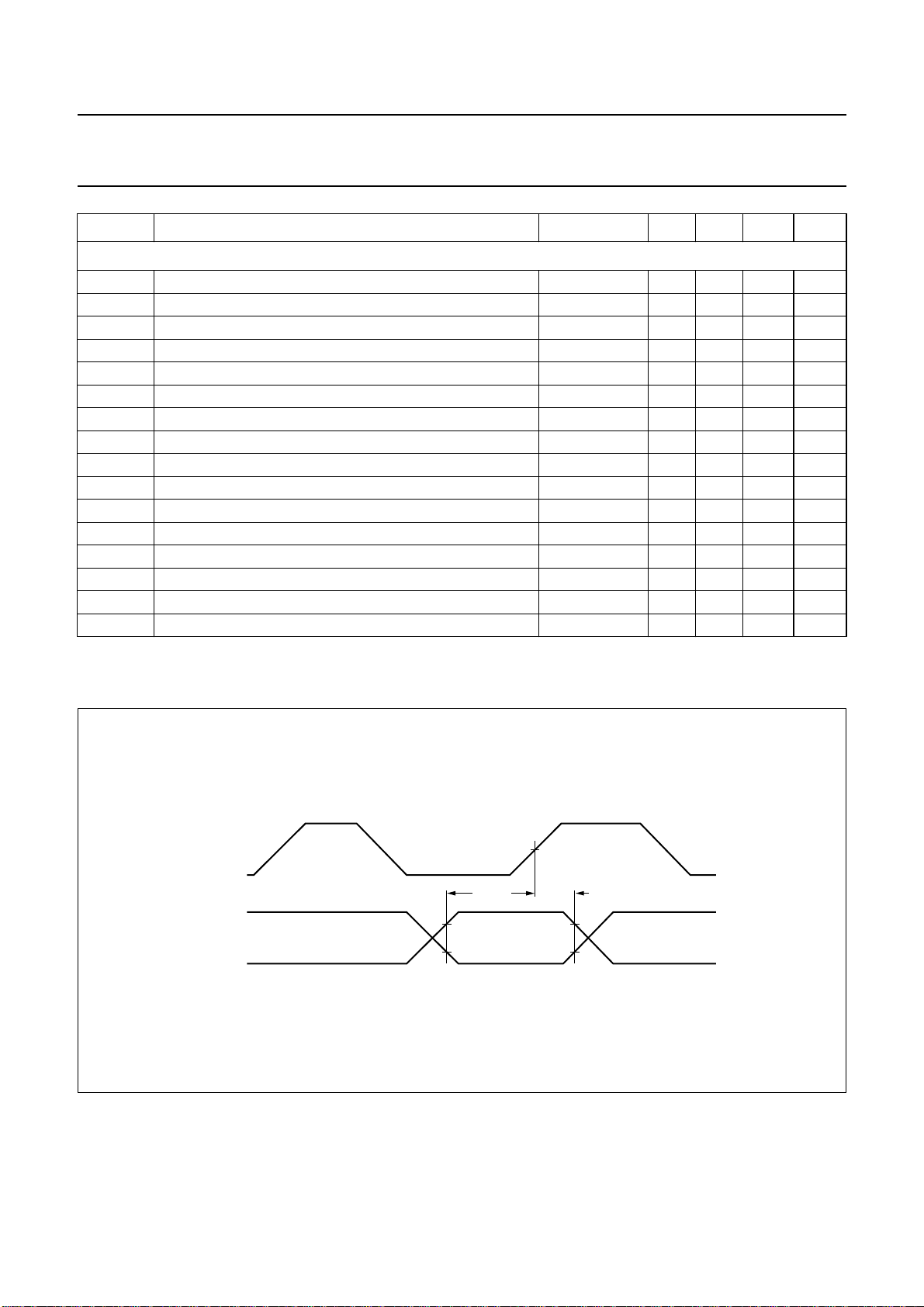
Philips Semiconductors Product specification
Digital camera USB interface IC SAA8117HL
SYMBOL PARAMETER CONDITIONS MIN. TYP. MAX. UNIT
PPG high-speed pulses for VGA sensors (see Fig.26)
t
d1
t
d2
t
d3
t
d4
t
d5
t
d6
t
d7
t
d8
t
WH(C1)
t
WH(C2)
t
WH(C3)
t
WL(SHP)
t
WL(SHD)
t
WL(RG)
t
WH(CLK1)
t
WH(CLK2)
Note
1. Load capacity = 11 pF; V
delay between rising edge C2 and rising edge C1 61 62 63 ns
delay between rising edge C3 and rising edge C2 61 62 63 ns
delay between rising edge SHP and falling edge C3 −1.5 −1 +0.5 ns
delay between falling edge SHD and rising edge C2 8 9 10 ns
delay between rising edge SHD and rising edge C3 −12 −11 −10 ns
delay between rising edge RG and rising edge C1 −0.5 0 +0.5 ns
delay between rising edge C1 and falling edge CLK1 18 19 21 ns
delay between rising edge C1 and rising edge CLK2 20 21 22 ns
C1 pulse width HIGH 81 82 − ns
C2 pulse width HIGH 81 82 − ns
C3 pulse width HIGH 82 85 − ns
SHP pulse width LOW 21 22 − ns
SHD pulse width LOW 43 44 − ns
RG pulse width LOW 21 22 − ns
CLK1 pulse width HIGH 81 82 − ns
CLK2 pulse width HIGH 41 43 − ns
DDD=VDDA
= 3.3 V; T
amb
=25°C.
handbook, full pagewidth
LCC
data input
Fig.24 Data input timing.
1999 Apr 02 50
t
su(i)D
t
h(i)D
FCE153
Page 51
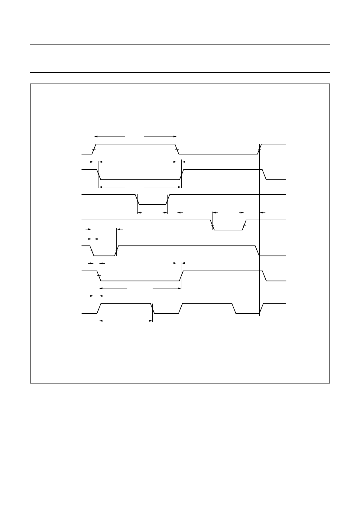
Philips Semiconductors Product specification
Digital camera USB interface IC SAA8117HL
t
handbook, full pagewidth
WH(C1)
C1
C2
SHP
SHD
RG
CLK1
CLK2
50% 50%
t
d1
50% 50%
t
WL(C2)
50% 50%
t
WL(SHP)
t
WL(RG)
t
d5
50% 50%
t
d6
50% 50%
t
WL(CLK1)
t
WH(CLK2)
50%
50%
t
d8
t
d2
t
d3
50% 50%
t
d7
t
WL(SHD)
50%
t
d4
FCE154
Fig.25 PPG high-speed pulses for PAL medium resolution sensors (mode 0).
1999 Apr 02 51
Page 52
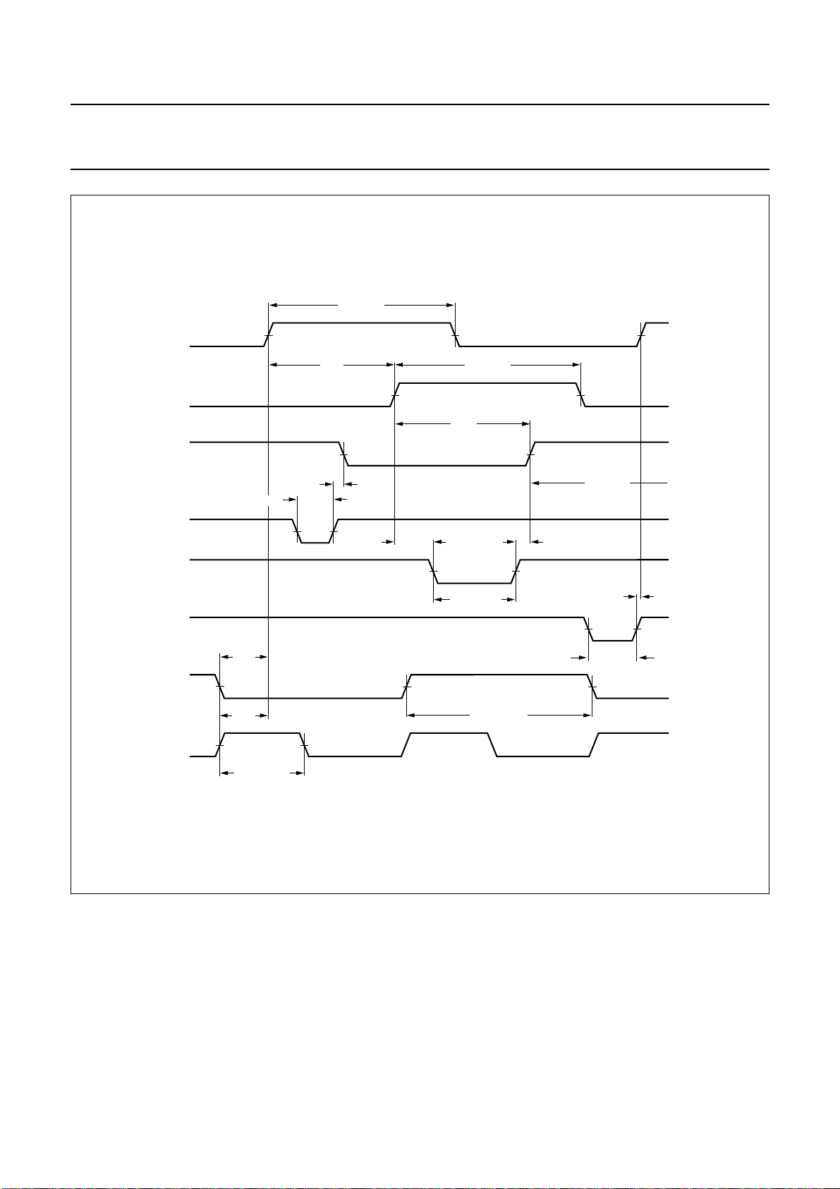
Philips Semiconductors Product specification
Digital camera USB interface IC SAA8117HL
handbook, full pagewidth
C1
C2
C3
SHP
SHD
RG
CLK1
t
WL(SHP)
t
d7
50%
t
WH(C1)
50% 50%
t
d1
50% 50%
50%
t
d3
50% 50%
t
d4
50%
t
WH(C2)
t
d2
50% 50%
t
WL(SHD)
t
WL(RG)
50%
t
WH(C3)
t
d5
t
d6
50% 50%
50%
t
d8
CLK2
50%
t
WH(CLK2)
50%
Fig.26 PPG high-speed pulses for VGA sensors (mode 2).
1999 Apr 02 52
t
WH(CLK1)
FCE155
Page 53
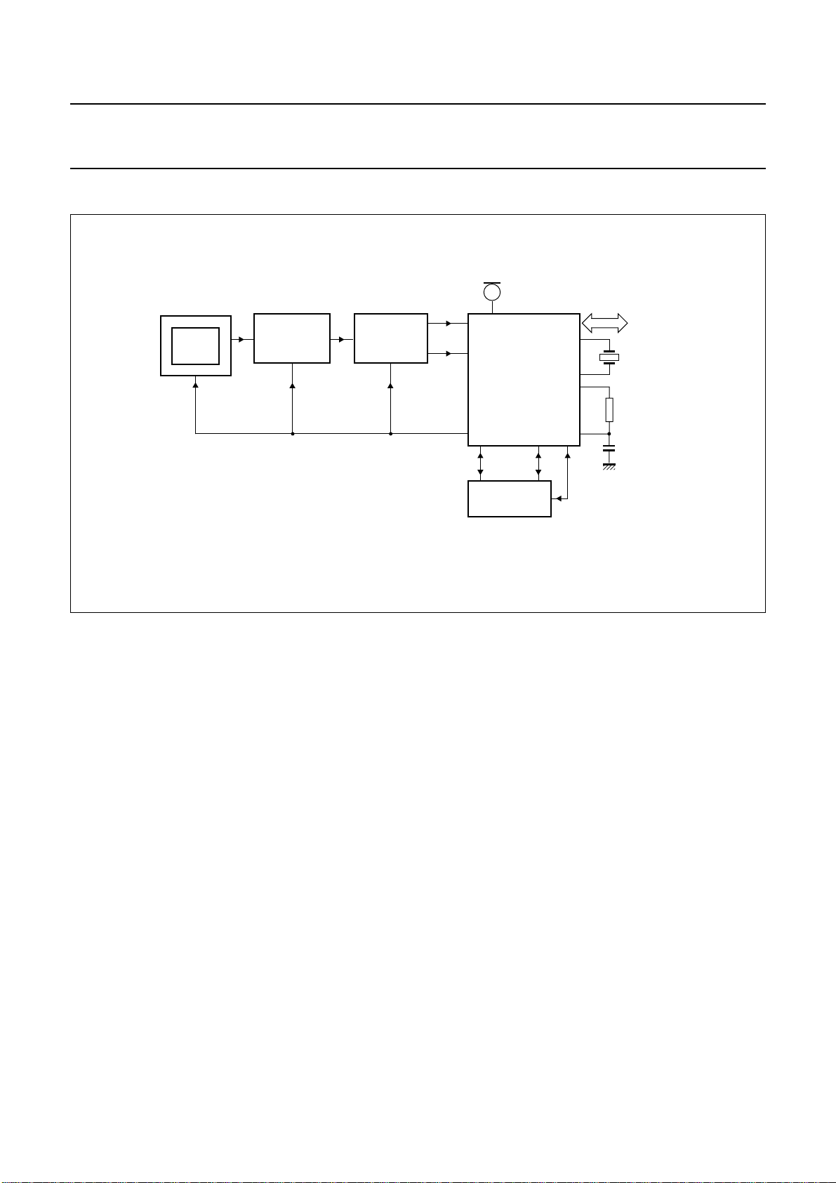
Philips Semiconductors Product specification
Digital camera USB interface IC SAA8117HL
14 APPLICATION INFORMATION
handbook, full pagewidth
SENSOR
TDA8784/87
PPG pulses
SAA8110G
SYNC
OR
SAA8112HL
YUV
SNERT
CONTROLLER
Fig.27 Application diagram.
MIC
SAA8117HL
CLOCKON
2
I
C-BUS
MICRO-
TRC
power
management
USB
48 MHz
FCE157
1999 Apr 02 53
Page 54
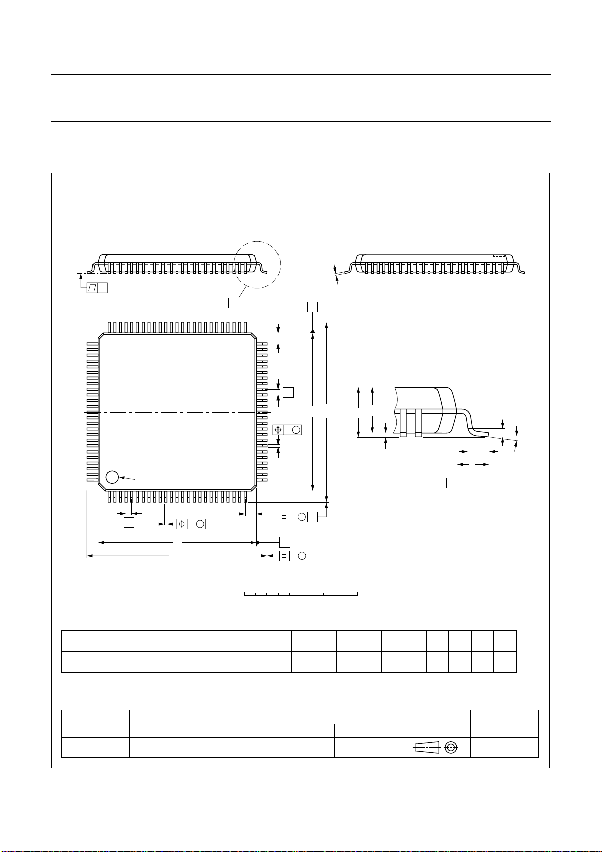
Philips Semiconductors Product specification
Digital camera USB interface IC SAA8117HL
15 PACKAGE OUTLINE
LQFP100: plastic low profile quad flat package; 100 leads; body 14 x 14 x 1.4 mm
c
y
100
X
75
76
51
50
Z
E
pin 1 index
26
1
e
w M
b
p
25
Z
D
D
H
D
b
B
e
w M
p
v M
v M
A
H
E
E
A
2
A
A
1
A
B
detail X
SOT407-1
(A )
3
θ
L
p
L
0 5 10 mm
scale
DIMENSIONS (mm are the original dimensions)
UNIT
mm
A
A1A2A3b
max.
0.20
1.6
0.05
1.5
1.3
0.25
cE
p
0.28
0.18
0.16
0.12
(1)
(1) (1)(1)
D
14.1
13.9
eH
H
14.1
13.9
0.5
16.25
15.75
Note
1. Plastic or metal protrusions of 0.25 mm maximum per side are not included.
OUTLINE
VERSION
IEC JEDEC EIAJ
REFERENCES
SOT407-1
1999 Apr 02 54
D
E
16.25
15.75
LL
p
0.75
0.45
0.12 0.10.21.0
EUROPEAN
PROJECTION
Z
D
1.15
0.85
Zywv θ
E
1.15
0.85
o
7
o
0
ISSUE DATE
95-12-19
97-08-04
Page 55

Philips Semiconductors Product specification
Digital camera USB interface IC SAA8117HL
16 SOLDERING
16.1 Introduction to soldering surface mount
packages
This text gives a very brief insight to a complex technology.
A more in-depth account of soldering ICs can be found in
“Data Handbook IC26; Integrated Circuit Packages”
our
(document order number 9398 652 90011).
There is no soldering method that is ideal for all surface
mount IC packages. Wave soldering is not always suitable
for surface mount ICs, or for printed-circuit boards with
high population densities. In these situations reflow
soldering is often used.
16.2 Reflow soldering
Reflow soldering requires solder paste (a suspension of
fine solder particles, flux and binding agent) to be applied
to the printed-circuit board by screen printing, stencilling or
pressure-syringe dispensing before package placement.
Several methods exist for reflowing; for example,
infrared/convection heating in a conveyor type oven.
Throughput times (preheating, soldering and cooling) vary
between 100 and 200 seconds depending on heating
method.
Typical reflow peak temperatures range from
215 to 250 °C. The top-surface temperature of the
packages should preferable be kept below 230 °C.
If wave soldering is used the following conditions must be
observed for optimal results:
• Use a double-wave soldering method comprising a
turbulent wave with high upward pressure followed by a
smooth laminar wave.
• For packages with leads on two sides and a pitch (e):
– larger than or equal to 1.27 mm, the footprint
longitudinal axis is preferred to be parallel to the
transport direction of the printed-circuit board;
– smaller than 1.27 mm, the footprint longitudinal axis
must be parallel to the transport direction of the
printed-circuit board.
The footprint must incorporate solder thieves at the
downstream end.
• For packages with leads on four sides, the footprint must
be placed at a 45° angle to the transport direction of the
printed-circuit board. The footprint must incorporate
solder thieves downstream and at the side corners.
During placement and before soldering, the package must
be fixed with a droplet of adhesive. The adhesive can be
applied by screen printing, pin transfer or syringe
dispensing. The package can be soldered after the
adhesive is cured.
Typical dwell time is 4 seconds at 250 °C.
A mildly-activated flux will eliminate the need for removal
of corrosive residues in most applications.
16.3 Wave soldering
Conventional single wave soldering is not recommended
for surface mount devices (SMDs) or printed-circuit boards
with a high component density, as solder bridging and
non-wetting can present major problems.
To overcome these problems the double-wave soldering
method was specifically developed.
1999 Apr 02 55
16.4 Manual soldering
Fix the component by first soldering two
diagonally-opposite end leads. Use a low voltage (24 V or
less) soldering iron applied to the flat part of the lead.
Contact time must be limited to 10 seconds at up to
300 °C.
When using a dedicated tool, all other leads can be
soldered in one operation within 2 to 5 seconds between
270 and 320 °C.
Page 56

Philips Semiconductors Product specification
Digital camera USB interface IC SAA8117HL
16.5 Suitability of surface mount IC packages for wave and reflow soldering methods
PACKAGE
WAVE REFLOW
(1)
BGA, SQFP not suitable suitable
SOLDERING METHOD
HLQFP, HSQFP, HSOP, HTSSOP, SMS not suitable
(3)
PLCC
, SO, SOJ suitable suitable
LQFP, QFP, TQFP not recommended
SSOP, TSSOP, VSO not recommended
(2)
(3)(4)
(5)
suitable
suitable
suitable
Notes
1. All surface mount (SMD) packages are moisture sensitive. Depending upon the moisture content, the maximum
temperature (with respect to time) and body size of the package, there is a risk that internal or external package
cracks may occur due to vaporization of the moisture in them (the so called popcorn effect). For details, refer to the
Drypack information in the
“Data Handbook IC26; Integrated Circuit Packages; Section: Packing Methods”
.
2. These packages are not suitable for wave soldering as a solder joint between the printed-circuit board and heatsink
(at bottom version) can not be achieved, and as solder may stick to the heatsink (on top version).
3. If wave soldering is considered, then the package must be placed at a 45° angle to the solder wave direction.
The package footprint must incorporate solder thieves downstream and at the side corners.
4. Wave soldering is only suitable for LQFP, TQFP and QFP packages with a pitch (e) equal to or larger than 0.8 mm;
it is definitely not suitable for packages with a pitch (e) equal to or smaller than 0.65 mm.
5. Wave soldering is only suitable for SSOP and TSSOP packages with a pitch (e) equal to or larger than 0.65 mm; it is
definitely not suitable for packages with a pitch (e) equal to or smaller than 0.5 mm.
1999 Apr 02 56
Page 57
Philips Semiconductors Product specification
Digital camera USB interface IC SAA8117HL
17 DEFINITIONS
Data sheet status
Objective specification This data sheet contains target or goal specifications for product development.
Preliminary specification This data sheet contains preliminary data; supplementary data may be published later.
Product specification This data sheet contains final product specifications.
Limiting values
Limiting values given are in accordance with the Absolute Maximum Rating System (IEC 134). Stress above one or
more of the limiting values may cause permanent damage to the device. These are stress ratings only and operation
of the device at these or at any other conditions above those given in the Characteristics sections of the specification
is not implied. Exposure to limiting values for extended periods may affect device reliability.
Application information
Where application information is given, it is advisory and does not form part of the specification.
18 LIFE SUPPORT APPLICATIONS
These products are not designed for use in life support appliances, devices, or systems where malfunction of these
products can reasonably be expected to result in personal injury. Philips customers using or selling these products for
use in such applications do so at their own risk and agree to fully indemnify Philips for any damages resulting from such
improper use or sale.
19 PURCHASE OF PHILIPS I
Purchase of Philips I
components in the I2C system provided the system conforms to the I2C specification defined by
Philips. This specification can be ordered using the code 9398 393 40011.
2
C COMPONENTS
2
C components conveys a license under the Philips’ I2C patent to use the
1999 Apr 02 57
Page 58

Philips Semiconductors Product specification
Digital camera USB interface IC SAA8117HL
NOTES
1999 Apr 02 58
Page 59

Philips Semiconductors Product specification
Digital camera USB interface IC SAA8117HL
NOTES
1999 Apr 02 59
Page 60

Philips Semiconductors – a worldwide company
Argentina: see South America
Australia: 34 Waterloo Road, NORTH RYDE, NSW 2113,
Tel. +61 2 9805 4455, Fax. +61 2 9805 4466
Austria: Computerstr. 6, A-1101 WIEN, P.O. Box 213,
Tel. +43 1 60 101 1248, Fax. +43 1 60 101 1210
Belarus: Hotel Minsk Business Center, Bld. 3, r. 1211, Volodarski Str. 6,
220050 MINSK, Tel. +375 172 20 0733, Fax. +375 172 20 0773
Belgium: see The Netherlands
Brazil: see South America
Bulgaria: Philips Bulgaria Ltd., Energoproject, 15th floor,
51 James Bourchier Blvd., 1407 SOFIA,
Tel. +359 2 68 9211, Fax. +359 2 68 9102
Canada: PHILIPS SEMICONDUCTORS/COMPONENTS,
Tel. +1 800 234 7381, Fax. +1 800 943 0087
China/Hong Kong: 501 Hong Kong Industrial Technology Centre,
72 Tat Chee Avenue, Kowloon Tong, HONG KONG,
Tel. +852 2319 7888, Fax. +852 2319 7700
Colombia: see South America
Czech Republic: see Austria
Denmark: Sydhavnsgade 23, 1780 COPENHAGEN V,
Tel. +45 33 29 3333, Fax. +45 33 29 3905
Finland: Sinikalliontie 3, FIN-02630 ESPOO,
Tel. +358 9 615 800, Fax. +358 9 6158 0920
France: 51 Rue Carnot, BP317, 92156 SURESNES Cedex,
Tel. +33 1 4099 6161, Fax. +33 1 4099 6427
Germany: Hammerbrookstraße 69, D-20097 HAMBURG,
Tel. +49 40 2353 60, Fax. +49 40 2353 6300
Hungary: see Austria
India: Philips INDIA Ltd, Band Box Building, 2nd floor,
254-D, Dr. Annie Besant Road, Worli, MUMBAI 400 025,
Tel. +91 22 493 8541, Fax. +91 22 493 0966
Indonesia: PT Philips Development Corporation, Semiconductors Division,
Gedung Philips, Jl. Buncit Raya Kav.99-100, JAKARTA 12510,
Tel. +62 21 794 0040 ext. 2501, Fax. +62 21 794 0080
Ireland: Newstead, Clonskeagh, DUBLIN 14,
Tel. +353 1 7640 000, Fax. +353 1 7640 200
Israel: RAPAC Electronics, 7 Kehilat Saloniki St, PO Box 18053,
TEL AVIV 61180, Tel. +972 3 645 0444, Fax. +972 3 649 1007
Italy: PHILIPS SEMICONDUCTORS, Piazza IV Novembre 3,
20124 MILANO, Tel. +39 2 6752 2531, Fax. +39 2 6752 2557
Japan: Philips Bldg 13-37, Kohnan 2-chome, Minato-ku,
TOKYO 108-8507, Tel. +81 3 3740 5130, Fax. +81 3 3740 5077
Korea: Philips House, 260-199 Itaewon-dong, Yongsan-ku, SEOUL,
Tel. +82 2 709 1412, Fax. +82 2 709 1415
Malaysia: No. 76 Jalan Universiti, 46200 PETALING JAYA, SELANGOR,
Tel. +60 3 750 5214, Fax. +60 3 757 4880
Mexico: 5900 Gateway East, Suite 200, EL PASO, TEXAS 79905,
Tel. +9-5 800 234 7381, Fax +9-5 800 943 0087
Middle East: see Italy
Netherlands: Postbus 90050, 5600PB EINDHOVEN, Bldg.VB,
Tel. +3140 2782785, Fax. +31 40 27 88399
New Zealand: 2 WagenerPlace, C.P.O. Box1041, AUCKLAND,
Tel. +649 8494160, Fax. +64 9 849 7811
Norway: Box 1, Manglerud0612, OSLO,
Tel. +4722 748000, Fax. +47 22 74 8341
Pakistan: see Singapore
Philippines: Philips Semiconductors Philippines Inc.,
106 ValeroSt. SalcedoVillage, P.O. Box 2108 MCC, MAKATI,
Metro MANILA, Tel.+63 2816 6380, Fax. +63 2 817 3474
Poland: Ul. Lukiska 10, PL 04-123 WARSZAWA,
Tel. +48 22 612 2831, Fax. +48 22 612 2327
Portugal: see Spain
Romania: see Italy
Russia: Philips Russia, Ul. Usatcheva 35A, 119048 MOSCOW,
Tel. +7 095 755 6918, Fax. +7 095 755 6919
Singapore: Lorong 1, Toa Payoh, SINGAPORE 319762,
Tel. +65 350 2538, Fax. +65 251 6500
Slovakia: see Austria
Slovenia: see Italy
South Africa: S.A. PHILIPS Pty Ltd., 195-215 Main Road Martindale,
2092 JOHANNESBURG, P.O. Box 7430 Johannesburg 2000,
Tel. +27 11 470 5911, Fax. +27 11 470 5494
South America: Al. Vicente Pinzon, 173, 6th floor,
04547-130 SÃO PAULO, SP, Brazil,
Tel. +55 11 821 2333, Fax. +55 11 821 2382
Spain: Balmes 22, 08007 BARCELONA,
Tel. +34 93 301 6312, Fax. +34 93 301 4107
Sweden: Kottbygatan 7, Akalla, S-16485 STOCKHOLM,
Tel. +46 8 5985 2000, Fax. +46 8 5985 2745
Switzerland: Allmendstrasse 140, CH-8027 ZÜRICH,
Tel. +41 1 488 2741 Fax. +41 1 488 3263
Taiwan: Philips Semiconductors, 6F, No. 96, Chien Kuo N. Rd., Sec. 1,
TAIPEI, Taiwan Tel. +886 2 2134 2886, Fax. +886 2 2134 2874
Thailand: PHILIPS ELECTRONICS (THAILAND) Ltd.,
209/2 Sanpavuth-Bangna Road Prakanong, BANGKOK 10260,
Tel. +66 2 745 4090, Fax. +66 2 398 0793
Turkey: Talatpasa Cad. No. 5, 80640 GÜLTEPE/ISTANBUL,
Tel. +90 212 279 2770, Fax. +90 212 282 6707
Ukraine: PHILIPS UKRAINE, 4 Patrice Lumumba str., Building B, Floor 7,
252042 KIEV, Tel. +380 44 264 2776, Fax. +380 44 268 0461
United Kingdom: Philips Semiconductors Ltd., 276 Bath Road, Hayes,
MIDDLESEX UB3 5BX, Tel. +44 181 730 5000, Fax. +44 181 754 8421
United States: 811 East Arques Avenue, SUNNYVALE, CA 94088-3409,
Tel. +1 800 234 7381, Fax. +1 800 943 0087
Uruguay: see South America
Vietnam: see Singapore
Yugoslavia: PHILIPS, Trg N. Pasica 5/v, 11000 BEOGRAD,
Tel. +381 11 62 5344, Fax.+381 11 63 5777
For all other countries apply to: Philips Semiconductors,
International Marketing & Sales Communications, Building BE-p, P.O. Box 218,
5600 MD EINDHOVEN, The Netherlands, Fax. +31 40 27 24825
© Philips Electronics N.V. 1999 SCA63
All rights are reserved. Reproduction in whole or in part is prohibited without the prior written consent of the copyright owner.
The information presented in this document does not form part of any quotation or contract, is believed to be accurate and reliable and may be changed
without notice. No liability will be accepted by the publisher for any consequence of its use. Publication thereof does not convey nor imply any license
under patent- or other industrial or intellectual property rights.
Internet: http://www.semiconductors.philips.com
Printed in The Netherlands 545006/750/01/pp60 Date of release: 1999 Apr 02 Document order number: 9397 750 04381
 Loading...