

Page 1

INTEGRATED CIRCUITS
DATA SH EET
SAA8116
DigitalPC-camerasignalprocessor
including microcontroller and USB
interface
Product specification
Supersedes data of 2000 Dec 6
File under Integrated Circuits, IC22
2001 May 04
Page 2

Philips Semiconductors Product specification
Digital PC-camera signal processor including
microcontroller and USB interface
FEATURES
• Embedded microcontroller (80C51 core based) for
control loops Auto Optical Black (AOB), Auto White
Balance (AWB), AutoExposure (AE) and USB interface
control
• Compliant for VGA CCD and VGA CMOS sensors
(RGB Bayer)
• USB 1.1 compliant bus-powered USB device with
integrated power management and POR circuit
• RGB processing
• Optical black processing
• Defect pixel concealment
• Programmable colour matrix
• RGB to YUV transform
• Programmable gamma correction (including knee)
• Programmable edge enhancement
• Video formatter with SIF/QSIF downscaler
• Compression engine
• Flexible Measurement Engine (ME) with up to eight
measurements per frame
• Internal Pulse Pattern Generator (PPG) for wide range
of VGA CCDs (Sony, Sharp and Panasonic) and frame
rate selection
• ProgrammableH and V timing for thesupport of CMOS
sensors
• Programmable output pulse for switched mode power
supply of the sensor
• 3-wireinterface to control anexternal pre-processor IC,
such as the TDA8787A: Correlated Double
Sampling (CDS), Automatic Gain Control (AGC) and
10-bit ADC
• Analog microphone/audio input to USB: Low DropOut
(LDO) supply filter, microphone supply, low noise
amplifier, programmable amplifier, PLL and ADC
• Integrated analog USB driver (ATX)
• Integrated main oscillator, including a clock PLL, which
derives 48 MHzmain systemclock froma 12 or48 MHz
fundamental crystal.
APPLICATION
• USB PC-camera (video and audio).
GENERAL DESCRIPTION
The SAA8116 is a highly integrated third generation
USB PC-camera ICs. It is the successor to the
SAA8112HL and SAA8115HL. It processes the digitized
sensor data and converts it to a high quality, compressed
YUV signal. Together with the audio signal, this video
signal is then properly formatted in USB packets.
In addition, an 80C51 microcontroller derivative with five
I/O ports, I2C-bus, 512 bytes of RAM and 32 kbytes of
program memory is embedded in the SAA8116. The
microcontroller is used in combination with the
programmable statistical measurement capabilities to
provideadvanced AE, AWBand AOB.Themicrocontroller
is also used to control the USB interface.
SAA8116
ORDERING INFORMATION
TYPE
NUMBER
SAA8116HL LQFP100 plastic low profile quad flat package; 100 leads; body 14 × 14 × 1.4 mm SOT407-1
SAA8116ET TFBGA112 plastic thin fine-pitch ball grid array package; 112 balls; body 7 × 7 × 0.8 mm SOT630-1
2001 May 04 2
NAME DESCRIPTION VERSION
PACKAGE
Page 3

Philips Semiconductors Product specification
Digital PC-camera signal processor including
SAA8116
microcontroller and USB interface
QUICK REFERENCE DATA
Measured over full voltage and temperature range: VDD= 3.3 V ±10% and T
SYMBOL PARAMETER CONDITIONS MIN. TYP. MAX. UNIT
V
DD
I
DD(tot)
V
i
V
o
f
(i)xtal
supply voltage 3.0 3.3 3.6 V
total supply current VDD= 3.3 V; T
=25°C (typ.) − 85
amb
input voltage 3.0V<VDD< 3.6 V low voltage TTL compatible V
output voltage 3.0V<VDD< 3.6 V low voltage TTL compatible V
crystal input frequency note 3 − 12 or 48 − MHz
δ crystal frequency duty factor − 50 − %
P
tot
T
stg
T
amb
T
j
total power dissipation; note 1 VDD= 3.3 V; T
=25°C (typ.) − 280 350 mW
amb
storage temperature −55 − +150 °C
ambient temperature 0 25 70 °C
junction temperature T
=70°C −40 − +125 °C
amb
Notes
1. Typical: VGA at 15 fps.
2. Maximum: SIF at 30 fps.
3. The crystal input frequency can be 12 or 48 MHz, depending on the use of the internal CPLL (selectable via
pin XSEL).
= 0 to 70 °C; unless specified.
amb
(1)
105
(2)
mA
2001 May 04 3
Page 4

This text is here in white to force landscape pages to be rotated correctly when browsing through the pdf in the Acrobat reader.This text is here in
_white to force landscape pages to be rotated correctly when browsing through the pdf in the Acrobat reader.This text is here inThis text is here in
white to force landscape pages to berotated correctly when browsing through the pdf in theAcrobat reader. white to force landscape pages to be...
2001 May 04 4
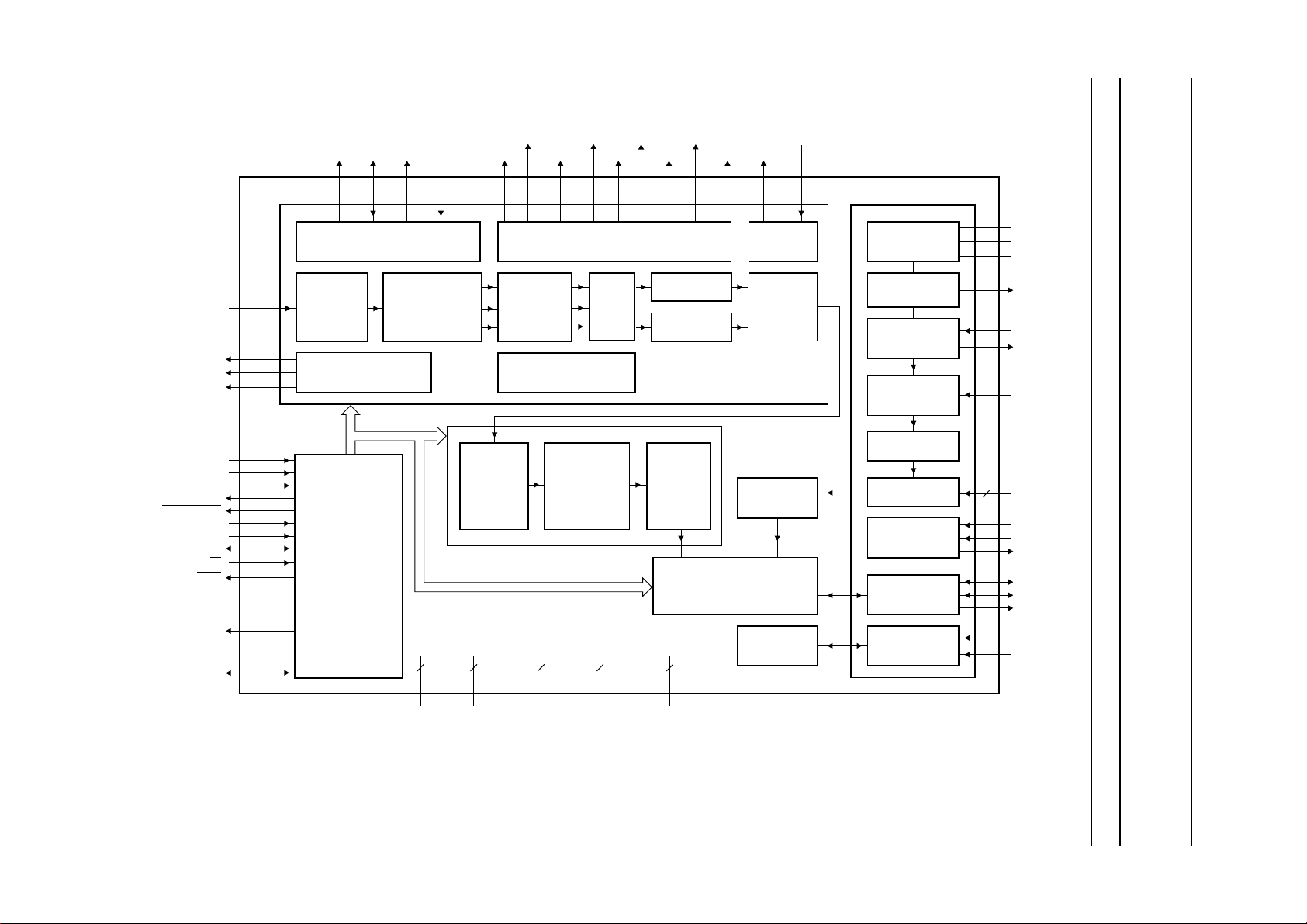
BLOCK DIAGRAM
Digital PC-camera signal processor including
microcontroller and USB interface
Philips Semiconductors Product specification
PXL9 to PXL0
STROBE
SDATA
SCLK
GPI1
GPI2
GPI3
LED
FULLPOWER
SNAPRES
PRIVRES
SDA, SCL
EA
ALE, PSEN
AD14 to AD8
P0.7 to P0.0
11, 12,
13, 14,
15, 16,
17, 18,
19, 20
25
27
26
34
70
71
4
89
28
29
33, 32
54
49, 50
48, 51, 47,
52, 46, 53,
45
39, 38, 40,
37, 41, 35,
42, 36
H
V ASCLK PCLK
VSP
WINDOW TIMING AND
CONTROL REFERENCE TIMING
PRE-
PROCESSING
PRE-PROCESSING
80C51
MICROCONTROLLER
RECONSTRUCTION
INTERFA CE
2
V
DDA1,
V
DDA2
RGB
72, 81
FV1, FV2
VIDEO
FORMA TTER
VFC
3
75, 78, 68
AGND1 to
AGND3
FV3, FV4
RGB
PROCESSING
MEASUREMENT ENGINE
ROG
FH1, FH2
PULSE PATTERN GENERATOR
RGB TO
COMPRESSION
ENGINE
SAA8116
2
V
DDD1,
V
DDD2
56, 21
V
6
DD1
V
DD6
BCP, DCP
CRSTRGFS, FCDS
PROCESSING
YUV
PROCESSING
TRANSFER
BUFFER
8
7, 30, 43,
76, 87, 99
to
8, 31, 44, 77,
88, 100, 55, 22
GND1 to
GND8
SMP RESERVED1
Y
UV
USB
INTERFACE
RESERVED2, RESERVED3
94 64 83, 8423, 245, 692979391, 903, 981, 29109695
MODE
DECODER
4 : 2 : 2
FORMATTER
AUDIO
DECIMATION
POWER
MANAGEMENT
ANALOG MODULES
LDO
SUPPLY
FILTER
MICROPHONE
SUPPLY
AUDIO
LOW NOISE
AMPLIFIER
PROGRAMMABLE
AUDIO GAIN
AMPLIFIER
AUDIO PLL
AUDIO ADC
OSCILLATOR
AND CPLL
ATX
POR
65,
66,
57
58
59
60
61
62
63
67
3
85
74
73
80
79
82
86
69
LDOIN
LDOFIL
LDOOUT
MICSUPPLY
MICIN
LNAOUT
PGAININ
V
ref1,
V
ref2,
V
ref3
XSEL
XIN
XOUT
ATXDP
ATXDN
DELAYATT
PSEL
PORE
FCE673
SAA8116
Fig.1 Block diagram (LQFP100).
Page 5
This text is here in white to force landscape pages to be rotated correctly when browsing through the pdf in the Acrobat reader.This text is here in
_white to force landscape pages to be rotated correctly when browsing through the pdf in the Acrobat reader.This text is here inThis text is here in
white to force landscape pages to berotated correctly when browsing through the pdf in theAcrobat reader. white to force landscape pages to be...
2001 May 04 5
Digital PC-camera signal processor including
microcontroller and USB interface
Philips Semiconductors Product specification
PXL9 to PXL0
STROBE
SDATA
SCLK
GPI1
GPI2
GPI3
LED
FULLPOWER
SNAPRES
PRIVRES
SDA, SCL
EA
ALE, PSEN
AD14 to AD8
P0.7 to P0.0
F2, F1,
G3, G1,
G2, H3,
H1, H2,
J3, J1
J4
K3
M2
M5
D12
D11
C1
A6
M3
L3
K5, L4
K11
K10, M11
M10, M12,
L10, J9,
K9, L12,
M9
M7, L7, K7,
L6, L8, L5,
M8, K6
H
V ASCLK PCLK
VSP
WINDOW TIMING AND
CONTROL REFERENCE TIMING
PRE-
PROCESSING
PRE-PROCESSING
INTERFA CE
80C51
MICROCONTROLLER
RECONSTRUCTION
2
V
DDA1,
V
DDA2
RGB
C12, B9
E1E3C4A4
FORMA TTER
VFC
3
AGND1 to
AGND3
FV3, FV4
FV1, FV2
VIDEO
FH1, FH2
C2,
D4,
A3
B1
PULSE PATTERN GENERATOR
RGB
PROCESSING
MEASUREMENT ENGINE
SAA8116
2
V
DDD1,
V
DDD2
J11, J2
D9, C10, E11
ROG
CRSTRGFS, FCDS
C6
RGB TO
YUV
COMPRESSION
ENGINE
6
D3, K4, K8,
B11, B7, C3
V
to
DD1
V
DD6
BCP, DCP
D2,
A5B3C5B5,
D1
PROCESSING
PROCESSING
TRANSFER
BUFFER
8
E2, M4, L9, A11,
B6, A2, K12, K1
GND1 to
GND8
SMP RESERVED1
K2,
L1
Y
UV
USB
INTERFACE
RESERVED2, RESERVED3
B4 G10 A8,
FORMATTER
DECIMATION
MANAGEMENT
MODE
DECODER
4 : 2 : 2
AUDIO
POWER
B8
ANALOG MODULES
LDO
SUPPLY
FILTER
MICROPHONE
SUPPLY
AUDIO
LOW NOISE
AMPLIFIER
PROGRAMMABLE
AUDIO GAIN
AMPLIFIER
AUDIO PLL
AUDIO ADC
OSCILLATOR
AND CPLL
ATX
POR
J12
J10
H11
H12
H10
G11
G12
F12,
F11,
E12
C7
B12
C11
A9
A10
C8
A7
D10
3
LDOIN
LDOFIL
LDOOUT
MICSUPPLY
MICIN
LNAOUT
PGAININ
V
ref1,
V
ref2,
V
ref3
XSEL
XIN
XOUT
ATXDP
ATXDN
DELAYATT
PSEL
PORE
MGU263
SAA8116
Fig.2 Block diagram (TFBGA112).
Page 6

Philips Semiconductors Product specification
Digital PC-camera signal processor including
SAA8116
microcontroller and USB interface
PINNING
SYMBOL PIN
(1)
FV1 1 D4 O vertical CCD transfer pulse output (or general purpose output)
FV2 2 B1 O vertical CCD transfer pulse output (or general purpose output)
FV3 3 C2 O vertical CCD transfer pulse output (or general purpose output)
LED 4 C1 O output to drive LED
FS 5 D2 O data sample-and-hold pulse output to TDA8787A (SHD)
FCDS 6 D1 O preset sample-and-hold pulse output to TDA8787A (SHP)
V
DD1
7 D3 P supply voltage 1 for output buffers
GND1 8 E2 P ground 1 for output buffers
PCLK 9 E1 I pixel input clock
ASCLK 10 E3 O clock 1 (pixelclock) or clock 2(2 × pixel clock) outputfor ADC orCMOS
PXL9 11 F2 I pixel data input; bit9
PXL8 12 F1 I pixel data input; bit8
PXL7 13 G3 I pixel data input; bit 7
PXL6 14 G1 I pixel data input; bit 6
PXL5 15 G2 I pixel data input; bit 5
PXL4 16 H3 I pixel data input; bit 4
PXL3 17 H1 I pixel data input; bit 3
PXL2 18 H2 I pixel data input; bit 2
PXL1 19 J3 I pixel data input; bit 1
PXL0 20 J1 I pixel data input; bit 0
V
DDD2
21 J2 P supply voltage 2 for the digital core
GND8 22 K1 P ground 8 for input buffers and predrivers
BCP 23 K2 O optical black clamp pulse output to TDA8787A
DCP 24 L1 O dummy clamp pulse output to TDA8787A
STROBE 25 J4 O strobe signal output to TDA8787A or general purpose output of the
SCLK 26 M2 O serial clock output to TDA8787A or general purpose output of the
SDATA 27 K3 O serial data output to TDA8787A or general purpose output of the
SNAPRES 28 M3 I snapshot input or remote wake-up trigger input (programmable)
PRIVRES 29 L3 I privacy shutter input or remote wake-up trigger input (programmable)
V
DD2
30 K4 P supply voltage 2 for input buffers and predrivers
GND2 31 M4 P ground 2 for input buffers and predrivers
SCL 32 L4 I/O I
SDA 33 K5 I/O I
GPI1 34 M5 I general purpose input 1 (Port 4; bit 6)
P0.2 35 L5 I/O microcontroller Port 0 bidirectional (data - address); bit 2
P0.0 36 K6 I/O microcontroller Port 0 bidirectional (data - address); bit 0
BALL
(2)
TYPE
(3)
sensor
microcontroller
microcontroller
microcontroller
2
C-bus clock input/output (master/slave)
2
C-bus data input/output (master/slave)
DESCRIPTION
2001 May 04 6
Page 7

Philips Semiconductors Product specification
Digital PC-camera signal processor including
SAA8116
microcontroller and USB interface
SYMBOL PIN
(1)
P0.4 37 L6 I/O microcontroller Port 0 bidirectional (data - address); bit 4
P0.6 38 L7 I/O microcontroller Port 0 bidirectional (data - address); bit 6
P0.7 39 M7 I/O microcontroller Port 0 bidirectional (data - address); bit 7
P0.5 40 K7 I/O microcontroller Port 0 bidirectional (data - address); bit 5
P0.3 41 L8 I/O microcontroller Port 0 bidirectional (data - address); bit 3
P0.1 42 M8 I/O microcontroller Port 0 bidirectional (data - address); bit 1
V
DD3
43 K8 P supply voltage 3 for output buffers
GND3 44 L9 P ground 3 for output buffers
AD8 45 M9 O microcontroller Port 2 output (address); bit 0
AD10 46 K9 O microcontroller Port 2 output (address); bit 2
AD12 47 L10 O microcontroller Port 2 output (address); bit 4
AD14 48 M10 O microcontroller Port 2 output (address); bit 6
ALE 49 K10 O address latch enable output for external latch
PSEN 50 M11 O program store enable output for external memory (active LOW)
AD13 51 M12 O microcontroller Port 2 output (address); bit 5
AD11 52 J9 O microcontroller Port 2 output (address); bit 3
AD9 53 L12 O microcontroller Port 2 output (address); bit 1
EA 54 K11 I external access select input; internal (HIGH) or external (LOW)
GND7 55 K12 P ground 7 for input buffers and predrivers
V
DDD1
56 J11 P supply voltage 1 for the digital core
LDOIN 57 J12 P analog supply voltage for LDO supply filter
LDOFIL 58 J10 − external capacitor connection (filter of LDO)
LDOOUT 59 H11 − external capacitor connection (internal analog supply voltage for PLL;
MICSUPPLY 60 H12 O microphone supply output
MICIN 61 H10 I microphone input
LNAOUT 62 G11 O low noise amplifier output
PGAININ 63 G12 I programmable gain amplifier input
RESERVED1 64 G10 O test pin 1 (should be floating)
V
ref1
V
ref2
V
ref3
65 F12 I reference voltage 1 (used in the amplifier and the ADC)
66 F11 I reference voltage 2 (used in the ADC)
67 E12 I reference voltage 3 (used in the ADC)
AGND3 68 E11 P analog ground 3 for PLL; amplifier and ADC
PORE 69 D10 I external Power-on reset
GPI2 70 D12 I general purpose input 2 (Port 1; bit 4)
GPI3 71 D11 I general purpose input 3 (Port 3; bit 5)
V
DDA1
72 C12 P analog supply voltage for crystal oscillator (12 MHz, fundamental)
XOUT 73 C11 O oscillator output
XIN 74 B12 I oscillator input
AGND1 75 D9 P analog ground 1 for crystal oscillator
BALL
(2)
TYPE
(3)
program memory
amplifier and ADC)
DESCRIPTION
2001 May 04 7
Page 8

Philips Semiconductors Product specification
Digital PC-camera signal processor including
SAA8116
microcontroller and USB interface
SYMBOL PIN
V
DD4
(1)
76 B11 P supply voltage 4 for input buffers and predrivers
GND4 77 A11 P ground 4 for input buffers and predrivers
AGND2 78 C10 P analog ground 2 for ATX transceiver
ATXDN 79 A10 I/O negative driver of the differential data pair input/output (ATX)
ATXDP 80 A9 I/O positive driver of the differential data pair input/output (ATX)
V
DDA2
81 B9 P analog supply voltage 2 for ATX transceiver
DELAYATT 82 C8 O delayedattach control output; connected withpull-up resistor onATXDP
RESERVED2 83 A8 I test pin 2 (should be connected to GND)
RESERVED3 84 B8 I test pin 3 (should be connected to GND)
XSEL 85 C7 I crystal selection input
PSEL 86 A7 I POR selection input
V
DD5
87 B7 P supply voltage 5 for output buffers
GND5 88 B6 P ground 5 for output buffers
FULLPOWER 89 A6 O full power signal output (active LOW)
FH2 90 C6 O horizontal CCD transfer pulse output
FH1 91 B5 O horizontal CCD transfer pulse output
RG 92 A5 O reset output for CCD output amplifier gate
ROG 93 C5 O vertical CCD load pulse output
SMP 94 B4 O switch mode pulse output for CCD supply
H 95 A4 O horizontal synchronization pulse output
V 96 C4 I/O vertical synchronization pulse input/output
CRST 97 B3 O CCD charge reset output for shutter control
FV4 98 A3 O vertical CCD transfer pulse output
V
DD6
99 C3 P supply voltage 6 for output buffers
GND6 100 A2 P ground 6 for output buffers
BALL
(2)
TYPE
(3)
DESCRIPTION
(USB)
Notes
1. Pinning related to LQFP100 package.
2. Pinning related to TFBGA112 package.
3. I = input; O = output and P = power supply.
2001 May 04 8
Page 9

Philips Semiconductors Product specification
Digital PC-camera signal processor including
microcontroller and USB interface
handbook, full pagewidth
FV1
FV2
FV3
LED
FS
FCDS
V
DD1
GND1
PCLK
ASCLK
PXL9
PXL8
PXL7
PXL6
PXL5
PXL4
PXL3
PXL2
PXL1
PXL0
V
DDD2
GND8
BCP
DCP
STROBE
DD6
GND6
V
FV4
CRSTVH
99989796959493929190898887868584838281
100
1
2
3
4
5
6
7
8
9
10
11
12
13
14
15
16
17
18
19
20
21
22
23
24
SMP
ROGRGFH1
FH2
SAA8116
DD5
FULLPOWER
GND5
V
PSEL
XSEL
RESERVED3
DDA2
RESERVED2
DELAYATT
V
ATXDP
ATXDN
AGND2
GND4
V
8079787776
SAA8116
DD4
AGND1
75
74
XIN
73
XOUT
V
72
GPI3
71
70
GPI2
PORE
69
AGND3
68
V
67
V
66
ref2
V
65
ref1
RESERVED1
64
PGAININ
63
62
LNAOUT
MICIN
61
MICSUPPLY
60
LDOOUT
59
58
LDOFIL
LDOIN
57
V
56
DDD1
55
GND7
54
EA
AD9
53
AD11
52
5125
AD13
DDA1
ref3
26272829303132333435363738394041424344454647484950
SCL
SCLK
SDATA
SNAPRES
DD2
V
PRIVRES
GND2
SDA
GPI1
P0.2
P0.0
P0.4
Fig.3 Pin configuration (LQFP100).
2001 May 04 9
P0.6
P0.7
P0.5
P0.3
P0.1
DD3
V
GND3
AD8
AD10
AD12
AD14
ALE
FCE674
PSEN
Page 10

Philips Semiconductors Product specification
Digital PC-camera signal processor including
microcontroller and USB interface
handbook, halfpage
M
L
K
J
H
G
F
E
D
C
B
A
SAA8116ET
246891011121357
SAA8116
FCE778
Fig.4 Ball configuration; bottom view of ball array (TFBGA112).
2001 May 04 10
Page 11

Philips Semiconductors Product specification
Digital PC-camera signal processor including
microcontroller and USB interface
Pinning for TFBGA112
BALL SYMBOL
A1 n.c.
A2 GND6
A3 FV4
A4 H
A5 RG
A6
FULLPOWER
A7 PSEL
A8 RESERVED2
A9 ATXDP
A10 ATXDN
A11 GND4
A12 n.c.
B1 FV2
B2 n.c.
B3 CRST
B4 SMP
B5 FH1
B6 GND5
B7 V
DD5
B8 RESERVED3
B9 V
DDA2
B10 n.c.
B11 V
DD4
B12 XIN
C1 LED
C2 FV3
C3 V
DD6
C4 V
C5 ROG
C6 FH2
C7 XSEL
C8 DELAYATT
C9 n.c.
C10 AGND2
C11 XOUT
C12 V
DDA1
D1 FCDS
BALL SYMBOL
D2 FS
D3 V
DD1
D4 FV1
D9 AGND1
D10 PORE
D11 GPI3
D12 GPI2
E1 PCLK
E2 GND1
E3 ASCLK
E10 n.c.
E11 AGND3
E12 V
ref3
F1 PXL8
F2 PXL9
F3 n.c.
F10 n.c.
F11 V
F12 V
ref2
ref1
G1 PXL6
G2 PXL5
G3 PXL7
G10 RESERVED1
G11 LNAOUT
G12 PGAININ
H1 PXL3
H2 PXL2
H3 PXL4
H10 MICIN
H11 LDOOUT
H12 MICSUPPLY
J1 PXL0
J2 V
DDD2
J3 PXL1
J4 STROBE
J9 AD11
J10 LDOFIL
J11 V
DDD1
SAA8116
BALL SYMBOL
J12 LDOIN
K1 GND8
K2 BCP
K3 SDATA
K4 V
K5 SDA
K6 P0.0
K7 P0.5
K8 V
K9 AD10
K10 ALE
K11
K12 GND7
L1 DCP
L2 n.c.
L3 PRIVRES
L4 SCL
L5 P0.2
L6 P0.4
L7 P0.6
L8 P0.3
L9 GND3
L10 AD12
L11 n.c.
L12 AD9
M1 n.c.
M2 SCLK
M3 SNAPRES
M4 GND2
M5 GPI1
M6 n.c.
M7 P0.7
M8 P0.1
M9 AD8
M10 AD14
M11
M12 AD13
DD2
DD3
EA
PSEN
2001 May 04 11
Page 12

Philips Semiconductors Product specification
Digital PC-camera signal processor including
microcontroller and USB interface
FUNCTIONAL DESCRIPTION
The SAA8116 video processor has a very high level of
programmability:118 (8-bit) registers arededicated forthe
Video Signal Processor (VSP), including Pulse Pattern
Generator (PPG) and Measurement Engine (ME), plus
23 registers for the Video Formatter and
Compressor (VFC). The SAA8116 can accept 8 to 10-bit
digital datafrom variousVGA sensors: CCD(progressive)
or CMOS, with or without colour filters (see Table 1).
Synchronization and video windows
CCD SENSOR PULSE PATTERN GENERATOR
The SAA8116 incorporates aPPG function, which can be
used for VGA CCD sensors, see Table 1.
Depending on the sensor type, an external inverter driver
isrequired toconvert the3.3 V pulsesto avoltage suitable
for the CCD sensor used.
Theactive videosize is640 × 480 forVGA. ThetotalH × V
size is 823 × 486 for VGA.
A total of 19 internal registers make a high level of
flexibility available for the PPG.
FLEXIBLE HV TIMING
The PPG module is not used with CMOS sensors. The
SAA8116 provides some flexibility on the frame size to
increase the range of applicable sensors (see Table 1). It
is possible to program the position, width and polarity of
the H and V signals. The output clock for the CMOS
sensor is selectable between single and double pixel
clock, including a programmable polarity.
The HV timing module can serve both as master orslave.
When servingas aslave, the V pulseonly is needed since
the H pulse is internally derived from V by programming
the number of pixels per line.
VIDEO WINDOWS
Several registers allow the definition of the optical black
window, the active video input window, the active video
output window and the measurement windows.
Table 1 Typical SAA8116 compatible sensors
VGA CCD Sony ICX098AK
VGA CMOS Philips UPA1021
Other sensors all sensors that fulfil the following
SENSOR
TYPE
SAA8116
BRAND PART NUMBER
Panasonic MN37771PT
Sharp LZ24BP
Hyundai HV7131B
Photobit PB-0320
criteria:
• B and W; RGB Bayer colour filter
• 8-bit, 9-bit or 10-bit output
• CMOS or CCD sensors
• progressive
2001 May 04 12
Page 13
Philips Semiconductors Product specification
Digital PC-camera signal processor including
microcontroller and USB interface
Video signal processor
OPTICAL BLACK PROCESSING
The first processing block of the SAA8116 is a digital
clamp(denoted asPRE-PROCESSINGin Fig.1).Itis used
to align the optical black level to zero or to any arbitrary
value.
The average value of the black is measured in the
programmable optical black window and sent to the
microcontroller for adjustment, if necessary. The value
fixed by the microcontroller is subtracted from the
incoming data stream.
The optical black window has a fixed size of 16 pixels
(horizontally) by 128 (vertically); the position of this
window is fully programmable.
Each of the four colour filter inputs has its own offset and
gain.
DEFECT PIXEL CONCEALMENT
Up to 128 Defect Pixel Coordinates (DPC) can be taken
into account forconcealment. The method is basedeither
on a horizontal linear interpolation, or on a copy of a
neighbouring pixel of the same colour.
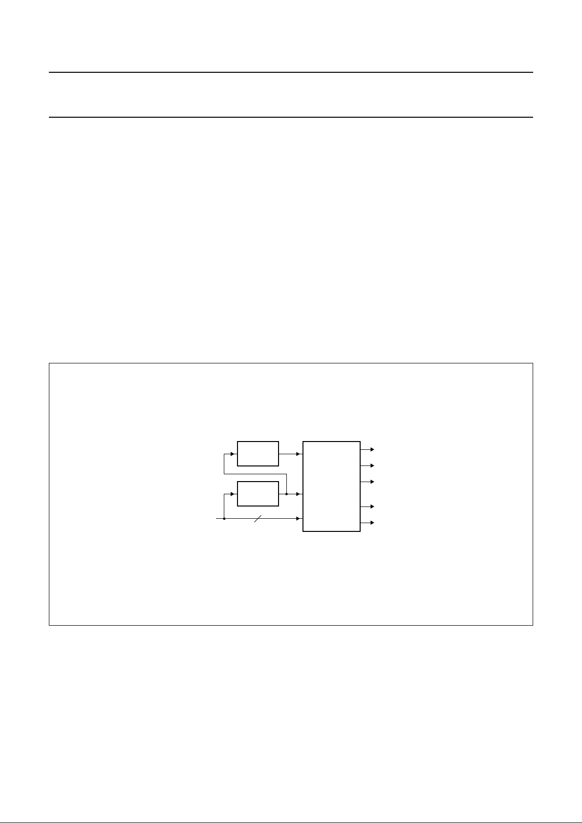
RGB COLOUR RECONSTRUCTOR
In the RGB colour reconstructor (denoted as RGB
RECONSTRUCTION in Fig.1), an RGB triplet is
interpolated for every pixel on a 3 × 3 neighbourhood
matrix.
With B and W sensors, the RGB colour reconstructor can
be disabled, thus maintaining the full sensor resolution.
Vertical contours and video level information (white clip)
are extracted at this stage (see Fig.5).
SAA8116
handbook, full pagewidth
CCD inputs
LINE
MEMORY
RGB
LINE
MEMORY
10
COLOUR
SEPARATION
FCE340
Fig.5 RGB reconstructor diagram.
R
G
B
White clip
Edges
2001 May 04 13
Page 14
Philips Semiconductors Product specification
Digital PC-camera signal processor including
SAA8116
microcontroller and USB interface
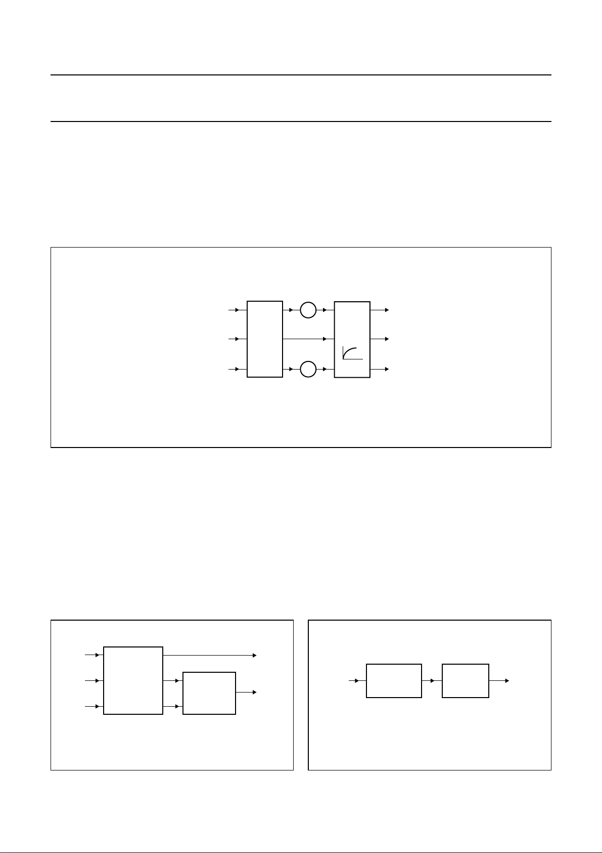
COLOUR MATRIX
A programmable 3 × 3 colour matrix (see Fig.6) is usedto convert the extractedcolour information, R, G and B fromthe
sensor colour space to a standard RGB colour space.
With B and W sensors, a unity matrix is used.
To control the white balance, the gain of the red and blue stream can be changed.
Gamma and knee are combined in one function with adjustable gain.
handbook, full pagewidth
R or (2R-G)
G or Y G
B or (2B-G)
COLOUR
MATRIX
R
B
gain
×
gain
×
R
GAMMA/
KNEE
B
FCE742
Fig.6 RGB processing diagram.
YUV PROCESSING
Following the RGB processing,the R, G and Bsignals are
converted to YUV 4 :2:2 by a fixed matrix (see Fig.7).
Then, the luminance and chrominance signals are
processed separately.
Theluminance processingconsists of edgeenhancement.
Thisfeature isvery flexible.First, itis possibleto adjustthe
bandwidth and the level of the edge detection. Secondly,
the amount of edge enhancement can be independently
adjusted for the horizontal or vertical edge or for the high
or low frequency edge.
R
G
B
CONVERSION
MATRIX
DOWN-
SAMPLING
AND MUX
FCE342
Y
UV
The chrominance processing consists of a colour killer
(white clip) and a UV gain control (see Fig.8). Processing
is done on the multiplexed two-times-downsampled
UV chrominance signals. The sensor input is used to kill
the colour of over-exposed pixels. It is possible to adjust
the number of pixels on which the correction is applied.
The YUV processing block concludes with separate gain
controls on the Y, U and V signals. These gains can be
used to fine tune the Y, U and V colour balance and also
to adjust the luminance and saturation without disturbing
the AE and AWB control loops.
handbook, halfpage
UV
WHITE CLIP
UV GAIN
CONTROL
FCE743
UV
Fig.7 RGB to YUV conversion.
2001 May 04 14
Fig.8 UV processing.
Page 15
Philips Semiconductors Product specification
Digital PC-camera signal processor including
microcontroller and USB interface
MEASUREMENT ENGINE
The ME extracts statistical information from the video
stream. These measurements are used for the
auto-control loops in the microcontroller (AWB, AE
and AGC).They canalso beusedfor otherpurposes,such
as colourdetection. The measurements areperformed on
pre-formatted Y, U and V streams. It is possible to
measure the accumulated value of the Y, U or V samples
either in the full active video window or in a simple
programmable window.
Five parallelmeasurements ofthe luminance canbe done
for the auto exposure, each based on a proper window.
Y, U and V can be measured independently for the auto
white balance, all based on the same window.
During each frame, the microcontroller has access to the
measured values of the previous frame.
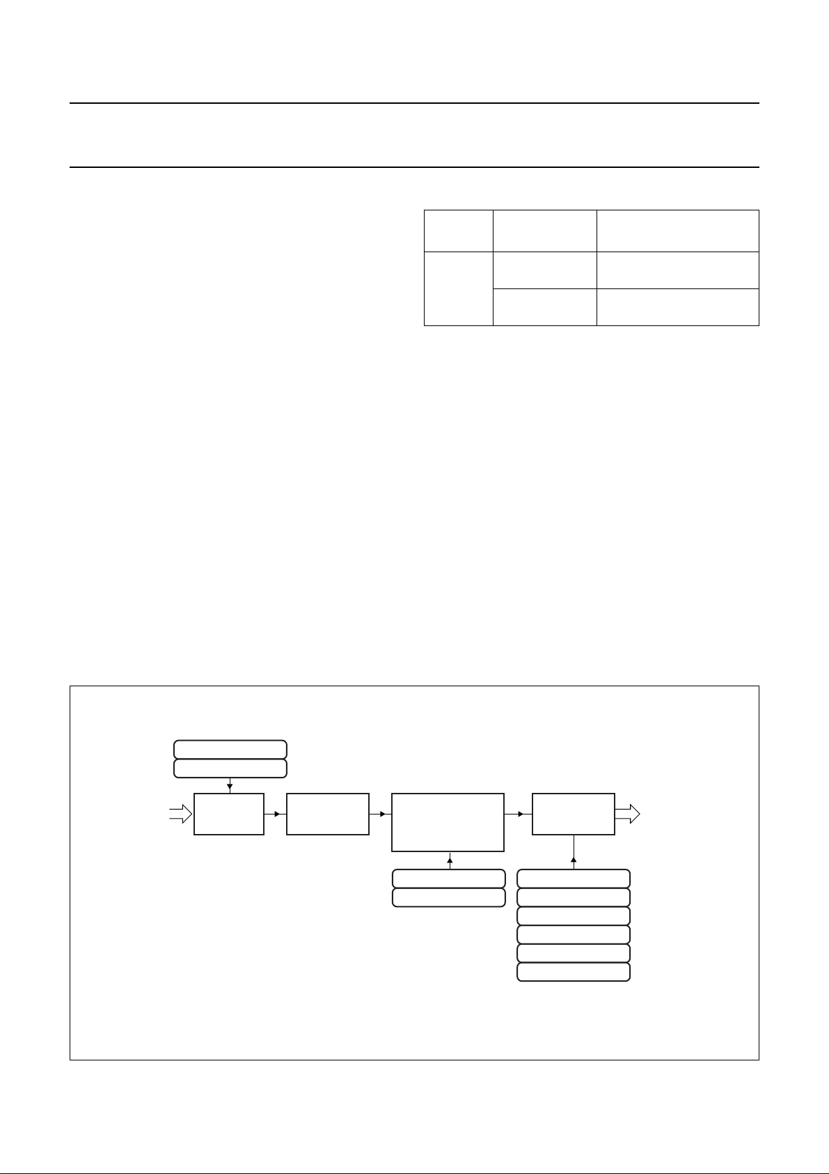
Video formatter
This block is used to convert the YUV 4 : 2 : 2 format to
4:2:0 required by the compression engine. The
incoming 4:2:2 data is vertically filtered. In raw mode,
this block is bypassed to create a full resolution snapshot.
The formatter can also perform downscaling to SIF and
QSIF (see Table 2).
Table 2 Scaler modes
SENSOR
VGA SIF 320 × 240 scaled half horizontally
Compression engine
The compression engine module (see Fig.9) can process
VGA, SIF and QSIF, based on a Philips proprietary
algorithm. The compression ratio is continuously
programmable by setting a maximum bit cost limit. Input
data can also be a raw RGB sensor data to perform
optimum snapshot processing in the host software.
The compression engine uses several strategies and
Q-tables for optimum performance at a wide range of
compression ratios (upto 8×). The required table must be
selected via software. One table is optimized for
compressing the raw VGA data.
Real time decoding can be done in software on any
Pentium or AMD-K6 platform.
TYPE
SAA8116
OUTPUT
FORMAT
QSIF 160 × 120 scaled quarter
SCALER MODES
and vertically
horizontally and vertically
To avoid aliasing, this formatter also contains horizontal
and vertical low pass pre-filters before downscaling.
handbook, full pagewidth
YUV7 to
YUV0
PREFILTER_SEL_UV
PREFILTER_SEL_Y
PREFILTER
HORIZONTAL
DOWNSCALING
Fig.9 The video formatter and compression engine.
DATA FORMATTER
+
VERTICAL
DOWN SAMPLING
VF_LIMITER
SCALE_DATA
COMPRESSION
ENGINE
TABLE_SELECT
LDC
C_BITCOST_MSB
C_BITCOST_LSB
C_THRESHOLD_MSB
C_THRESHOLD_LSB
FCE744
to
transfer
buffer
2001 May 04 15
Page 16

Philips Semiconductors Product specification
Digital PC-camera signal processor including
microcontroller and USB interface
Table 3 gives the available output formats and frame rates.
Table 3 Video formats
FORMAT FRAME RATE COMPRESSION MODE
VGA 5 raw; compressed
5 compressed
10 compressed
15 compressed
30 compressed
SIF 5 compressed and uncompressed
10 compressed
15 compressed
20 compressed
24 compressed
30 compressed
QSIF 5 compressed and uncompressed
10 compressed and uncompressed
15 compressed and uncompressed
20 compressed and uncompressed
24 compressed and uncompressed
30 compressed and uncompressed
SAA8116
The compressed data is streamed into a video FIFO, ready to be packed into USB formatted data blocks.
2001 May 04 16
Page 17

Philips Semiconductors Product specification
Digital PC-camera signal processor including
microcontroller and USB interface
Universal serial bus 1.1 core
The USB core combines all functionalities for a USB 1.1
compliant full speed device. It formats the actual packets
(video and audio) that are transferred to the USB and
passes the incoming packetsto the right end-point buffer.
The end-point setup is composed of control, generic and
isochronous types (see Table 4). All end-points can be
enabled or disabled, except control end-points.
All enabled end-points generate interrupts to the
embedded microcontrollerwhen theyneed tobe serviced.
The microcontroller can then use a set of commands via
the internal parallel interface.
Table 4 Mapping of logical to physical end-point numbers for the end-points
LOGICAL
END-POINT
0 0 control out 16 no
1 2 generic out 8 no
2 4 generic in 8 no
3 5 generic in 8 no
4 6 isochronous in 92 yes
5 7 isochronous in programmable multi-buffered
PHYSICAL
END-POINT
1 control in 16 no
3 generic in 8 no
END-POINT TYPE DIRECTION BUFFER SIZE
The video FIFO size allows demarcation of the video
frames using one or more 0-length packets.
The core also includes VID class support for the video
end-point: headersand trailersenable data tobe attached
to the video frames that are passed over the USB. Eight
1-byte registers are dedicated for the headers, while four
registerscomprise thetrailers. Eachofthe registerscanbe
programmed by the microcontroller. An extra register,
TR_HT_CONTROL, specifies how many bytes are
inserted before or after the video data.
SAA8116
DOUBLE
BUFFERED
ATX interface
The SAA8116 contains an analog bus driver, called
the ATX. This driver incorporates a differential amplifier
and twosingle-ended buffers for thereceiver part and two
single-ended buffers for the transmitter part.
The interface to the bus consists of a differential data pair
(ATXDN and ATXDP).
Microcontroller
The embeddedmicrocontroller is an 80C654core (80C51
family). Ports P0 and P2 (plus ALE and PSEN) are
available for connection to an emulator or to an external
program EPROM (32 kbytes max.).
The microcontroller can control the AOB, AE and AWB
loops, and can download the settings for the internal
registers from an optional EEPROM at power-up or reset.
Aparallel interfaceis usedto communicatewith allinternal
modules, based on the MOVX@DPTR instruction.
The microcontroller includes the following features:
• 32 kbytes internal ROM
• 512 bytes RAM
• Hardware multi-master I2C-bus interface (the
microcontroller can be used either as slave or master):
P1.7 and P1.6
• Power-down mode
• Two timers
• P0 and P2 are pull-up ports
• Three pins are available as general purpose inputs:
GPI1 (P4.6), GPI2 (P1.4) and GPI3 (P3.5).
2001 May 04 17
Page 18

Philips Semiconductors Product specification
Digital PC-camera signal processor including
SAA8116
microcontroller and USB interface
Table 5 80C51 Special Function Registers (SFR)
SFR
NAME
B B register F0H B7 B6 B5 B4 B3 B2 B1 B0
ACC accumulator E0H ACC7 ACC6 ACC5 ACC4 ACC3 ACC2 ACC1 ACC0
SIADR serial interface address DBH SA6 SA5 SA4 SA3 SA2 SA1 SA0 GC
SIDAT serial interface data DAH SD7 SD6 SD5 SD4 SD3 SD2 SD1 SD0
SISTA serial interface status D9H ST7 ST6 ST5 ST4 ST3 0 0 0
SICON serial interface control D8H CR2 ENS1 STA STO SI AA CR1 CR0
PSW program status word D0H CY AC F0 RS1 RS0 OV − P
P4 Port 4 C0H P4.7 P4.6 P4.5 P4.4 P4.3 P4.2 P4.1 P4.0
IP interrupt priority B8H − IP6 IP5 IP4 PT1 PX1 PT0 PX0
P3 Port 3 B0H
IE interrupt enable A8H
P2 Port 2 A0H (AD15) AD14 AD13 AD12 AD11 AD10 AD9 AD8
SBUF serial data buffer 99H −−−−−−−−
SCON serial controller 98H SM0 SM1 SM2 REN TB8 RB8 T1 R1
P1 Port 1 90H SDA SCL P1.5 P1.4 P1.3 P1.2 P1.1 P1.0
TH1 timer high 1 8DH −−−−−−−−
TH0 timer high 0 8CH −−−−−−−−
TL1 timer low 1 8BH −−−−−−−−
TL0 timer low 0 8AH −−−−−−−−
TMOD timer mode 89H GATE C/T M1 M0 GATE C/T M1 M0
TCON timer control 88H TF1 TR1 TF0 TR0 IE1 IT1 IE0 IT0
PCON power control 87H −−−−−−PD IDL
DPH data pointer high 83H −−−−−−−−
DPLl data pointer low 82H −−−−−−−−
SP stack pointer 81H SP7 SP6 SP5 SP4 SP3 SP2 SP1 SP0
P0 Port 0 80H P0.7 P0.6 P0.5 P0.4 P0.3 P0.2 P0.1 P0.0
DESCRIPTION
SFR
ADDRESS
76543210
RD WR T1 T0 INT1 INT0 TXD RXD
EA IE6 IE5 IE4 ET1 EX1 ET0 EX0
DATA BIT
Audio
The SAA8116 contains a microphone supply, including a
low-drop electronic supply filter, and an amplifier circuit
composedof twostages: aLow NoiseAmplifier (LNA) and
a variable gain amplifier (VGA).The LNA has a fixed gain
of 30 dB while the VGA can be programmed between
0 and 30 dB in steps of 2 dB. The frequency transfer
characteristic of the audio path must be controlled via
external high-pass or low-pass filters.
2001 May 04 18
The PLL converts the 48 MHz to 256fs(fs= audio sample
frequency). There arethree modes for the PLL toachieve
the sample frequencies of 48, 44.1 and 32 kHz or their
derivatives (see Table 6).
Thebitstream ADCsamples themono audiosignal. Itruns
at an oversample rate of 256 times the base sample rate.
A decimator filtertransforms the bitstream outputto 16-bit
samples.
A digital mute option is available.
Page 19

Philips Semiconductors Product specification
Digital PC-camera signal processor including
microcontroller and USB interface
Table 6 ADC clock frequencies and sample frequencies
CLOCK
(MHz)
8.1920 1 32 4.096
11.2896 1 44.1 5.6448
12.2880 1 48 6.144
Note
1. Not supported.
DIVIDING
NUMBER
2 16 2.048
4 8 1.042
8 note 1 note 1
2 22.05 2.8224
4 11.025 1.4112
8 5.5125 0.7056
2 24 3.072
4 12 1.536
8 6 0.768
SAMPLE
FREQUENCY
(kHz)
ADC CLOCK
(MHz)
CLOCK PLL
The SAA8116runs onan internalmaster clock of48 MHz,
which can be derived from either a 48 or 12 MHz
fundamental crystal. When it is derived from a 12 MHz
fundamental crystal, an internal clock PLL transfers the
12 MHz to 48 MHz, with a 50% duty cycle.
A 48 MHz third overtone crystal can also be used but
requires an external LC circuit.
RING OSCILLATOR
To generate several time constants for power state
switching, a digital counter running on an integrated ring
oscillator is incorporated, thus saving pins and commonly
used external RC components.
POWER-ON RESET (POR)
APOR functionis integratedto generatea resetduring the
start-up of the power supply and during a power fail. It
includes a fixed threshold detector (2.6 V) and a reset
generator. The reset output has a built-in delay with a
duration determined by the ring oscillator(around 100 ms).
SAA8116
Power management
USB requires the device to switch power states. The
SAA8116 contains a power management module since
the completecamera maynot consumemore than500 µA
during theSUSPEND powerstate. Thisrequires that even
thecrystal oscillatormust be switchedoff. The SAA8116is
not functional exceptfor some logic that enables the ICto
wake up the camera.
The SAA8116 incorporatesremote wake-up (on twopins)
to signal the host to resume operation when triggered.
Thepower managementmodule alsosetsa flagin register
POWERMGT_STATUS. After a reset, the microcontroller
should check this register and find the cause of the
wake-up. Different causes may require different start-up
routines.
Miscellaneous functions
Some additional functions are integrated in the SAA8116
to provide a cost effective application.
SERIAL INTERFACE WITH THE PRE-PROCESSOR
With CCD image sensors, the pre-processor (e.g.
TDA8787A) iscontrolled overa 3-wireserial interface. Itis
adaptedto shiftout16 bit settings.For flexibility, theoutput
pins can also beprogrammed asthree generaloutput pins
using register PIN_CONFIG_1.
An external POR can be used.
MODE CONTROL
Twopins arededicated tocontrolthe operationalmodes of
the SAA8116 (see Table 7).
Table 7 Mode control
XS PS MODE
0 0 application mode (48 MHz crystal;
internal POR)
0 1 application mode (48 MHz crystal;
external POR)
1 0 application mode (12 MHz crystal;
internal POR)
1 1 application mode (12 MHz crystal;
external POR)
2001 May 04 19
Page 20

Philips Semiconductors Product specification
Digital PC-camera signal processor including
SAA8116
microcontroller and USB interface
CONTROL REGISTER DESCRIPTION
This specification gives an overview of all internal
registers. Several modules (VSP, VFC, PPG, USB, audio
and power management) communicate with the internal
microcontroller via a common parallel interface. The
protocol is based on a standard MOVX@DPTR
instruction. A relativeaddress (DPH) is usedto select one
Table 8 Register list
ADDRESS NAME FUNCTION FORMAT RANGE
Write registers
0 0x00H VSP_CONTROL0 control register for VSP data path see Table 9 n.a.
1 0x01H VSP_CONTROL1 control register for VSP data path see Table 10 n.a.
2 0x02H OB_K1 fixed optical black level for
K1 pixel
3 0x03H OB_K2 fixed optical black level for
K2 pixel
4 0x04H OB_K3 fixed optical black level for
K3 pixel
5 0x05H OB_K4 fixed optical black level for
K4 pixel
6 0x06H PRE_MAT_K1 pre-gain for K1 pixel byte
7 0x07H PRE_MAT_K2 pre-gain for K2 pixel byte
8 0x08H PRE_MAT_K3 pre-gain for K3 pixel byte
9 0x09H PRE_MAT_K4 pre-gain for K4 pixel byte
10 0x0AH WHITE_CLIP_THR threshold for white clip detector byte 768 + [0 to 255]
11 0x0BH reserved
12 0x0CH COL_MAT_P11 colour matrix coefficient p11 byte [−128 to 127]/16
13 0x0DH COL_MAT_P12 colour matrix coefficient p12 byte [−128 to 127]/16
14 0x0EH COL_MAT_P13 colour matrix coefficient p13 byte [−128 to 127]/16
15 0x0FH COL_MAT_P21 colour matrix coefficient p21 byte [−128 to 127]/16
16 0x10H COL_MAT_P22 colour matrix coefficient p22 byte [−128 to 127]/16
17 0x11H COL_MAT_P23 colour matrix coefficient p23 byte [−128 to 127]/16
18 0x12H COL_MAT_P31 colour matrix coefficient p31 byte [−128 to 127]/16
19 0x13H COL_MAT_P32 colour matrix coefficient p32 byte [−128 to 127]/16
20 0x14H COL_MAT_P33 colour matrix coefficient p33 byte [−128 to 127]/16
21 0x15H COL_MAT_RGAIN red gain for white balance
correction
22 0x16H COL_MAT_BGAIN blue gain for white balance
correction
23 0x17H GAMMA_KNEE control of gamma/knee level see Table 11 n.a.
24 0x18H VC_CNTRL vertical contour control see Table 12 n.a.
25 0x19H CLDLEV contour level dependency level byte [0 to 255]/2
of the modules (via Port 2), while register addresses and
data are exchanged via Port 0.
VSP, VFC and PPG registers
A first MOVX@DPTR instruction enables to select the
module (viaDPH) and theregister address. A secondone
communicates the data (read or write).
byte [−128 to 127]
byte [−128 to 127]
byte [−128 to 127]
byte [−128 to 127]
byte [0 to 255]/128
byte [0 to 255]/64
2001 May 04 20
Page 21

Philips Semiconductors Product specification
Digital PC-camera signal processor including
SAA8116
microcontroller and USB interface
ADDRESS NAME FUNCTION FORMAT RANGE
26 0x1AH HCLGAIN/HCHGAIN horizontal contour BPF low gain
(MS)/horizontal contour BP high
gain (LS)
27 0x1BH CNCLEV contour noise coring level 6 bits [0 to 63]/2
28 0x1CH CONGAIN contour gain factor 6 bits [0 to 63]/16
29 0x1DH YGAIN Y gain factor (luminance) byte [0 to 255]/128
30 0x1EH UGAIN U (B - Y) gain factor byte [0 to 255]/128
31 0x1FH VGAIN V (R - Y) gain factor byte [0 to 255]/128
32 0x20H AWB_A AWB_A (ME) byte [−128 to 127]/128
33 0x21H AWB_B AWB_B (ME) byte [−128 to 127]/128
34 0x22H AWB_C AWB_C (ME) byte [−128 to 127]/128
35 0x23H AWB_D AWB_D (ME) byte [−128 to 127]/128
36 0x24H AWB_E AWB_E (ME) byte [0 to 255]
37 0x25H AWB_F AWB_F (ME) byte [0to 255]
38 0x26H reserved
39 0x27H DMWSEL display measurement window
select
40 0x28H DISPLEV display level in use with several
display functions
41 0x29H DIG_SETUP setup in digital output byte [0 to 255]
42 0x2AH PRE_SI_LSB control data (LS byte) for analog
processing
43 0x2BH PRE_SI_MSB control data (MS byte) for analog
processing
44 0x2CH PIXCNT_PRESET_LSB preset value of pixel counter (by
default = 0)
45 0x2DH NLINE_PRESET_MSB numberof linesper frame + MSBs
of preset register (by default = 6)
46 0x2EH LINECNT_PRESET_LSB preset value for line counter; line
number 0 is undefined (by
default = 1)
47 0x2FH NPIX number of pixels per line (by
default = 55)
48 0x30H CTR_UPD_LINE number of line for double buffer
update control registers
49 0x31H OB_STARTLINE first line optical black window byte 2 × [0 to 255]
50 0x32H OB_STARTPIXEL first pixel optical black window byte 4 × [0 to 255]
51 0x33H PIX_START_ACTWIN_ME starting position of the active
window defining the ME windows
(by default = 15)
52 0x34H HREFSTART position of positive edge of HREF
on a line (by default = 3)
53 0x35H HOUT_PE_LSB position of positive edge of HOUT byte [0 to 255]
nibble [0 to 15]/16
see Table 13 n.a.
see Table 14 n.a.
byte [0 to 255]
byte [0 to 255]
byte [0 to 255]
see Table 15 n.a.
byte [1 to 255]
byte 768 + [0 to 255]
byte 1 + 2 × [0 to 255]
4 bits [0 to 15]
4 bits 2 × [0 to 15]
2001 May 04 21
Page 22

Philips Semiconductors Product specification
Digital PC-camera signal processor including
SAA8116
microcontroller and USB interface
ADDRESS NAME FUNCTION FORMAT RANGE
54 0x36H HOUT_NE_LSB position of negative edge of
HOUT
55 0x37H VOUT_HPE_LSB horizontal position of positive
edge of VOUT
56 0x38H VOUT_VPE_LSB vertical position of positive edge
of VOUT
57 0x39H VOUT_HNE_LSB horizontal position of negative
edge of VOUT
58 0x3AH VOUT_VNE_LSB vertical position of negative edge
of VOUT
59 0x3BH VHOUT_MSB_1 MSB of VHOUT position
definitions (part 1)
60 0x3CH VHOUT_MSB_2 MSB of VHOUT position
definitions (part 2)
61 0x3DH HOUTWIN_VPE_LSB vertical position of positive edge
of HOUT window
62 0x3EH HOUTWIN_VNE_LSB vertical position of negative edge
of HOUT window
63 0x3FH XSEL selects the number of extended
active pixels (by default = 0)
64 0x40H ME_WIN_START_AWB AWB_window (Vstart; Hstart) byte
65 0x41H ME_WIN_STOP_AWB AWB_window (Vstop; Hstop) byte
66 0x42H ME_WIN_START_AE_0 AE_window no. 0 (Vstart; Hstart) byte
67 0x43H ME_WIN_STOP_AE_0 AE_window no. 0 (Vstop; Hstop) byte
68 0x44H ME_WIN_START_AE_1 AE_window no. 1 (Vstart; Hstart) byte
69 0x45H ME_WIN_STOP_AE_1 AE_window no. 1 (Vstop; Hstop) byte
70 0x46H ME_WIN_START_AE_2 AE_window no. 2 (Vstart; Hstart) byte
71 0x47H ME_WIN_STOP_AE_2 AE_window no. 2 (Vstop; Hstop) byte
72 0x48H ME_WIN_START_AE_3 AE_window no. 3 (Vstart; Hstart) byte
73 0x49H ME_WIN_STOP_AE_3 AE_window no. 3 (Vstop; Hstop) byte
74 0x4AH ME_WIN_START_AE_4 AE_window no. 4 (Vstart; Hstart) byte
75 0x4BH ME_WIN_STOP_AE_4 AE_window no. 4 (Vstop; Hstop) byte
76 0x4CH DPCRAMPTR RAM write pointer for DPC RAM byte 3 × [0 to 127]
77 0x4DH DPCRAMDATA RAM write data DPC RAM byte [0 to 255]
78 0x4EH reserved
79 0x4FH reserved
80 0x50H TR_HEADER #0 data for header byte no. 0 byte
81 0x51H TR_HEADER #1 data for header byte no. 1 byte
82 0x52H TR_HEADER #2 data for header byte no. 2 byte
83 0x53H TR_HEADER #3 data for header byte no. 3 byte
84 0x54H TR_HEADER #4 data for header byte no. 4 byte
85 0x55H TR_HEADER #5 data for header byte no. 5 byte
86 0x56H TR_HEADER #6 data for header byte no. 6 byte
byte [0 to 255]
byte [0 to 255]
byte [0 to 255]
byte [0 to 255]
byte [0 to 255]
see Table 16 n.a.
see Table 17 n.a.
byte [0 to 255]
byte [0 to 255]
see Table 18 n.a.
2001 May 04 22
Page 23

Philips Semiconductors Product specification
Digital PC-camera signal processor including
SAA8116
microcontroller and USB interface
ADDRESS NAME FUNCTION FORMAT RANGE
87 0x57H TR_HEADER #7 data for header byte no. 7 byte
88 0x58H TR_TRAILER #0 data for trailer byte no. 0 byte
89 0x59H TR_TRAILER #1 data for trailer byte no. 1 byte
90 0x5AH TR_TRAILER #2 data for trailer byte no. 2 byte
91 0x5BH TR_TRAILER #3 data for trailer byte no. 3 byte
92 0x5CH TR_HT_CONTROL header trailer control see Table 19 n.a.
93 0x5DH SMP_PERIOD SMP period in
units 4 × clk48_period
94 0x5EH SMP_LOWTIME SMP low time in units
4 × clk48_period
95 0x5FH reserved
96 0x60H PPG_CONTROL_0 PPG control register 0
(by default = 0)
97 0x61H PPG_CONTROL_1 PPG control register 1
(by default = 64)
98 0x62H PPG_H_CTRL controls mode of FH1; FH2
and RG (by default = 0)
99 0x63H PPG_V_INV controls inversion of vertical FV1;
FV2; FV3; FV4 and ROG signals
(by default = 0)
100 0x64H PPG_H_INV controls inversion of horizontal
signals (by default = 0)
101 0x65H PPG_MISC_INV controls inversion of misc. signals
and sets additional mode controls
(by default = 0)
102 0x66H PPG_SHUTTERSPEED_V_LSB shutter speed line number
(by default = 0)
103 0x67H PPG_SHUTTERSPEED_H_LSB shutter speed CRST start
(by default = 0)
104 0x68H PPG_SHUTTERSPEED_MSB MSB for shutter speed control
(line number; CRST start)
(by default = 0)
105 0x69H PPG_BCP_START_LSB starting position control for BCP
pulse (by default = 0)
106 0x6AH PPG_BCP_STOP_LSB stopping position control for BCP
pulse (by default = 0)
107 0x6BH PPG_DCP_START_LSB starting position control for DCP
pulse (by default = 0)
108 0x6CH PPG_DCP_STOP_LSB stopping position control for DCP
pulse (by default = 0)
109 0x6DH PPG_BCP_DCP_MSB MSB for start/stopping position
control for BCP/DCP pulses
(by default = 0)
110 0x6EH PPG_ROG1_START_LSB starting position control for ROG1
pulse (by default = 0)
byte 1 + [0 to 255]
byte 1 + [0 to 255]
see Table 20 n.a.
see Table 21 n.a.
see Table 22 n.a.
see Table 23 n.a.
see Table 24 n.a.
see Table 25 n.a.
see Table 26
see Table 27
see Table 28 n.a.
see Table 29
see Table 30
see Table 31
see Table 32
see Table 33
see Table 34
2001 May 04 23
Page 24

Philips Semiconductors Product specification
Digital PC-camera signal processor including
SAA8116
microcontroller and USB interface
ADDRESS NAME FUNCTION FORMAT RANGE
111 0x6FH PPG_ROG1_STOP_LSB stopping position control for
ROG1 pulse (by default= 0)
112 0x70H PPG_ROG2_START_LSB starting position control for ROG2
pulse (by default = 0)
113 0x71H PPG_ROG2_STOP_LSB stopping position control for
ROG2 pulse (by default= 0)
114 0x72H PPG_ROG1_2_MSB MSB for start/stopping position
control for ROG1/2 pulses
(by default = 0)
115 0x73H VFC_CONTROL_0 control register for video formatter
and compression module
(by default = 1)
116 0x74H VFC_CONTROL_1 control register for video formatter
and compression module
(by default = 0)
117 0x75H VF_LIMITER sets value for limiter output of
video formatter (by default = 0)
118 0x76H C_bitcost_MSB bit cost for compression module
(MSB) (by default = 0)
119 0x77H C_bitcost_LSB bit cost for compression module
(LSB) (by default = 0)
120 0x78H C_THRESHOLD_MSB fixed length coding threshold for
compression module (MSB)
(by default = 0)
121 0x79H C_THRESHOLD_LSB fixed length coding threshold for
compression module (LSB)
(by default = 0)
122 0x7AH TR_CONTROL control registerfortransfer module
(video processing) (by default = 0)
123 0x7BH VFC_VS_V_SHFT V_shift of internal line counter
w.r.t. the VS pulse (by default = 0)
124 0x7CH reserved
125 0x7DH reserved
126 0x7EH PIN_CONFIG_0 control pin configuration see Table 41 n.a.
127 0x7FH PIN_CONFIG_1 control pin configuration see Table 42 n.a.
Read registers
192 0xC0H ME_AWB_Y_MSB MSB part of ME_AWB_Y byte [0 to 31]
193 0xC1H ME_AWB_U_MSB MSB part of ME_AWB_U byte [0 to 31]
194 0xC2H ME_AWB_V_MSB MSB part of ME_AWB_V byte [0 to 31]
195 0xC3H ME_AE_#0_MSB MSB part of ME_AE_no. 0 byte [0 to 31]
196 0xC4H ME_AE_#1_MSB MSB part of ME_AE_no. 1 byte [0 to 31]
197 0xC5H ME_AE_#2_MSB MSB part of ME_AE_no. 2 byte [0 to 31]
198 0xC6H ME_AE_#3_MSB MSB part of ME_AE_no. 3 byte [0 to 31]
199 0xC7H ME_AE_#4_MSB MSB part of ME_AE_no. 4 byte [0 to 31]
see Table 35
see Table 36
see Table 37
see Table 38
see Table 39 n.a.
see Table 40 n.a.
byte [0 to 255]
byte 28 × [0 to 255]
byte [0 to 255]
byte 28 × [0 to 255]
byte [0 to 255]
bit n.a.
3 bits [0 to 7]
2001 May 04 24
Page 25

Philips Semiconductors Product specification
Digital PC-camera signal processor including
SAA8116
microcontroller and USB interface
ADDRESS NAME FUNCTION FORMAT RANGE
200 0xC8H ME_AWB_Y_ISB ISB part of ME_AWB_Y byte [0 to 255]
201 0xC9H ME_AWB_U_ISB ISB part of ME_AWB_U byte [0 to 255]
202 0xCAH ME_AWB_V_ISB ISB part of ME_AWB_V byte [0 to 255]
203 0xCBH ME_AE_#0_ISB ISB part of ME_AE_no. 0 byte [0 to 255]
204 0xCCH ME_AE_#1_ISB ISB part of ME_AE_no. 1 byte [0 to 255]
205 0xCDH ME_AE_#2_ISB ISB part of ME_AE_no. 2 byte [0 to 255]
206 0xCEH ME_AE_#3_ISB ISB part of ME_AE_no. 3 byte [0 to 255]
207 0xCFH ME_AE_#4_ISB ISB part of ME_AE_no. 4 byte [0 to 255]
208 0xD0H ME_AWB_Y_LSB LSB part of ME_AWB_Y byte [0 to 255]
209 0xD1H ME_AWB_U_LSB LSB part of ME_AWB_U byte [0 to 255]
210 0xD2H ME_AWB_V_LSB LSB part of ME_AWB_V byte [0 to 255]
211 0xD3H ME_AE_#0_LSB LSB part of ME_AE_no. 0 byte [0 to 255]
212 0xD4H ME_AE_#1_LSB LSB part of ME_AE_no. 1 byte [0 to 255]
213 0xD5H ME_AE_#2_LSB LSB part of ME_AE_no. 2 byte [0 to 255]
214 0xD6H ME_AE_#3_LSB LSB part of ME_AE_no. 3 byte [0 to 255]
215 0xD7H ME_AE_#4_LSB LSB part of ME_AE_no. 4 byte [0 to 255]
216 0xD8H ME_OB_LEVEL measured optical black level byte [0 to 255]
217 0xD9H READBACK_RGAIN read back of double-buffered
RGAIN
218 0xDAH READBACK_BGAIN read back of double-buffered
BGAIN
byte [0 to 255]
byte [0 to 255]
Table 9 Register CONTROL 0 (address: 0x00H)
BIT
76543210
EN_CLK_DPC_RAM: control defect pixel concealment RAM clock
0 disabled
1 enabled
EN_DPC: control defect pixel concealment
0 disabled
1 enabled
CLK_IF_RESET: control clk1/clk2 interface
0 free running (by default)
1 reset
X toggle phase for line in colour separation
X toggle phase for pixel in colour separation
X reserved
FORCE_AWBVAL: control AWB window
0 enabled
1 disabled (integral AWB measurement)
X reserved
PARAMETER
2001 May 04 25
Page 26

Philips Semiconductors Product specification
Digital PC-camera signal processor including
microcontroller and USB interface
Table 10 Register CONTROL 1 (address: 0x01H)
BIT
PARAMETER
76543210
DISP_CNTRL: select display signal
0 0 no display
0 1 D_WC (white clipped pixels)
1 0 D_AWBVAL (pixels according to AWBVAL)
1 1 D_MWG (measurement windows)
RGB_SEP_OFF: RGB reconstructor for raw data mode
0 enabled (normal RGB mode)
1 disabled (raw data mode)
X X reserved
VCF_GAIN: vertical contour filter gain
0 double
1 normal
WH_CL_MAP: white clip mapping on UV-grid
0 0 [0 0 1 0 0] spreading filter
0 1 [0 1 1 1 0] spreading filter
X X [1 1 1 1 1] spreading filter
SAA8116
Table 11 Register GAMMA_KNEE (address: 0x17H)
BIT
76543210
control scaler (5/8 gain)
0 disabled (transparent mode)
1 enabled (normal operation)
control knee
0 disabled
1 enabled
XXXXXXgamma balance [0 to 63]/64
Table 12 Register VC_CNTRL (address: 0x18H)
BIT
76543210
control vertical contour horizontal low pass filter
0 disabled
1 enabled
X X X vertical contour COMB filter gain [0 to 7]/8
XXXXvertical contour gain [0 to 15]/16
PARAMETER
PARAMETER
2001 May 04 26
Page 27

Philips Semiconductors Product specification
Digital PC-camera signal processor including
microcontroller and USB interface
Table 13 Register DMWSEL (address: 0x27H)
BIT
76543210
X undefined
display measurement window #A for line #3
0 disabled
1 enabled
display measurement window #B for line #2
0 disabled
1 enabled
display measurement window #A for line #2
0 disabled
1 enabled
X undefined
display measurement window #A for line #1
0 disabled
1 enabled
display measurement window #B for line #0
0 disabled
1 enabled
display measurement window #A for line #0
0 disabled
1 enabled
SAA8116
PARAMETER
Table 14 Register DISPLEV (address: 0x28H)
BIT
76543210
XXXXXXXXset defect pixel display level in defect pixel display mode [4 × [0 to 255]]
XXXX setY(luminance) display level to other display modes [16 × [0 to 15]]
X X set U display level to other display modes [64× [−2 to 1]]
X X set V display level to other display modes [64 × [−2 to 1]]
Table 15 Register NLINE_PRESET_MSB (address: 0x2DH)
BIT
76543210
X X bits 8 and 9 for PIXCNT_PRESET (by default = 0)
X bit 8 for LINECNT_PRESET (by default = 0; note 1)
XXXXXnumber of lines in a frame [480 + [0 to 31]] (by default = 6)
Note
1. Internal LINECNT range is [1 to 511]; no line zero.
2001 May 04 27
PARAMETER
PARAMETER
Page 28

Philips Semiconductors Product specification
Digital PC-camera signal processor including
microcontroller and USB interface
Table 16 Register VHOUT_MSB_1 (address: 0x3BH)
BIT
76543210
X X bits 8 and 9 for VOUT_HNE; note1
X X bits 8 and 9 for VOUT_HPE; note 1
X X bits 8 and 9 for HOUT_NE
X X bits 8 and 9 for HOUT_PE
Note
1. Internal LINECNT range is [1 to 511]; no line zero.
Table 17 Register VHOUT_MSB_2 (address: 0x3CH)
BIT
76543210
X X X reserved
X select HOUT polarity
X bit 8 for HOUTWIN_VNE; note 1
X bit 8 for HOUTWIN_VPE; note 1
X bit 8 for VOUT_VNE; note 1
X bit 8 for VOUT_VPE; note 1
SAA8116
PARAMETER
PARAMETER
Note
1. Internal LINECNT range is [1 to 511]; no line zero.
Table 18 Register XSEL (address: 0x3FH)
BIT
76543210
X X X reserved
XXXXXmode control for pixel extender
Table 19 Register TR_HT_CONTROL (address: 0x5CH
BIT
76543210
X undefined
HEAD_ENA: control header transfer
0 disabled
1 enabled
X X X HEAD_LEN: header length
TRAIL_ENA: control trailer transfer
0 disabled
1 enabled
X X TRAIL_LEN: trailer length
PARAMETER
PARAMETER
2001 May 04 28
Page 29

Philips Semiconductors Product specification
Digital PC-camera signal processor including
microcontroller and USB interface
Table 20 Register PPG_CONTROL_0 (address: 0x60H)
BIT
76543210
X X X undefined
SHUTTER_UPDATE_BUFFER: control shutter speed
0 immediate (by default)
1 buffered during vertical blanking
select PPG power mode
0 operational (by default)
1 resume
select PPG timing mode (VGA sensor)
0 0 0 frame rate = 30 fps (LLC = 24.0 MHz)
0 0 1 frame rate = 24 fps (LLC = 19.2 MHz)
0 1 0 frame rate = 20 fps (LLC = 16.0 MHz)
0 1 1 frame rate = 15 fps (LLC = 12.0 MHz)
1 0 0 frame rate = 10 fps (LLC = 8.0 MHz)
1 0 1 frame rate = 5 fps (LLC = 4.0 MHz)
1 1 X undefined
SAA8116
PARAMETER
2001 May 04 29
Page 30

Philips Semiconductors Product specification
Digital PC-camera signal processor including
microcontroller and USB interface
Table 21 Register PPG_CONTROL_1 (address: 0x61H)
BIT
76543210
X reserved
select frequency for compression clock CLK_C
0000 off
0001 2.0MHz
0010 2.4MHz
0011 4.0MHz
0100 4.8MHz
0101 6.0MHz
0110 8.0MHz
0111 9.6MHz
1000 12MHz (by default)
1001 16MHz
1010 19.2 MHz
1011 24MHz
1 1 X X reserved
select VGA sensor type
0 X reserved
1 0 VGA type 1 (Sharp LZ24BP; Sony ICX098AK)
1 1 VGA type 2 (Panasonic MN37771PT)
X reserved
SAA8116
PARAMETER
2001 May 04 30
Page 31

Philips Semiconductors Product specification
Digital PC-camera signal processor including
microcontroller and USB interface
Table 22 Register PPG_H_CTRL (address: 0x62H)
BIT
76543210
X reserved
set RG pulse width
0 nominal value
1 RG_SHORT: half of nominal value
FH2_CTRL; note 1
0 0 0 blanked to HIGH; starts LOW
0 0 1 blanked to LOW; starts HIGH
0 1 0 blanked to LOW; starts LOW
0 1 1 blanked to HIGH; starts HIGH
1 X 0 no horizontal blanking; pulse inverted
1 X 1 no horizontal blanking
FH1_CTRL; note 1
0 0 0 blanked to LOW; starts HIGH
0 0 1 blanked to HIGH; starts LOW
0 1 0 blanked to HIGH; starts HIGH
0 1 1 blanked to LOW; starts LOW
1 X 0 no horizontal blanking; pulse inverted
1 X 1 no horizontal blanking
SAA8116
PARAMETER
Note
1. If bits [5 to 3] equal bits [2 to 0] then FH2 is the inverse of FH1.
2001 May 04 31
Page 32

Philips Semiconductors Product specification
Digital PC-camera signal processor including
microcontroller and USB interface
Table 23 Register PPG_V_INV (address: 0x63H)
BIT
76543210
FV4_INV
0 negative pulses
1 positive pulses
FV3_INV
0 negative pulses
1 positive pulses
FV2_INV
0 positive pulses
1 negative pulses
FV1_INV
0 positive pulses
1 negative pulses
ROG1_INV; note 1
0 negative pulses
1 positive pulses
ROG2_INV; note 1
0 negative pulses
1 positive pulses
X X reserved
SAA8116
PARAMETER
Note
1. ROG1_INV and ROG2_INV are related to ROG_SEL (see Table 41; PIN_CONFIG_0[0]). If ROG_SEL = 0, then
ROG2_INV is activated (with Sony or Sharp CCD applications) and ROG1_INV is disabled. If ROG_SEL = 1, then
ROG1_INV is activated (with Panasonic CCD applications) and ROG2_INV is disabled.
2001 May 04 32
Page 33

Philips Semiconductors Product specification
Digital PC-camera signal processor including
microcontroller and USB interface
Table 24 Register PPG_H_INV (address: 0x64H)
BIT
76543210
CLK2_INV
0 nominal pulses
1 inverted pulses
CLK1_INV
0 nominal pulses
1 inverted pulses
FS_INV
0 negative pulses
1 positive pulses
FCDS_INV
0 negative pulses
1 positive pulses
RG_INV
0 negative pulses
1 positive pulses
X reserved
FH2_INV
0 positive pulses
1 negative pulses
FH1_INV
0 positive pulses
1 negative pulses
SAA8116
PARAMETER
2001 May 04 33
Page 34

Philips Semiconductors Product specification
Digital PC-camera signal processor including
microcontroller and USB interface
Table 25 Register PPG_MISC_INV (address: 0x65H)
BIT
76543210
X reserved
SELECT_FV3
0 FV3 equals FV2
1 FV3 equals FV4 (with VGA type 1 sensors)
X reserved
CRST_INV
0 negative pulses
1 positive pulses
BCP_INV
0 positive pulses
1 negative pulses
DCP_INV
0 positive pulses
1 negative pulses
H_INV
0 positive pulses
1 negative pulses
V_INV
0 positive pulses
1 negative pulses
SAA8116
PARAMETER
Table 26 Register PPG_SHUTTERSPEED_V_LSB (address: 0x66H)
BIT
76543210
XXXXXXXX8LSBs of line number (9 bits) on which shutter speed is updated
Table 27 Register PPG_SHUTTERSPEED_H_LSB (address: 0x67H)
BIT
76543210
XXXXXXXX8LSBs of pixel number (10 bits) on which shutter speed is updated
2001 May 04 34
PARAMETER
PARAMETER
Page 35

Philips Semiconductors Product specification
Digital PC-camera signal processor including
microcontroller and USB interface
Table 28 Register PPG_SHUTTERSPEED_MSB (address: 0x68H)
BIT
PARAMETER
76543210
XXXX reserved
SENSOR_TYPE
0 Sharp
1 Sony
X X 2 MSBs of pixel number (10 bits)
X MSB of line number (9 bits)
Table 29 Register PPG_BCP_START_LSB (address: 0x69H)
BIT
PARAMETER
76543210
XXXXXXXX8LSBs of pixel number (10 bits) where BCP starts
Table 30 Register PPG_BCP_STOP_LSB (address: 0x6AH)
SAA8116
BIT
76543210
XXXXXXXX8LSBs of pixel number (10 bits) where BCP stops
Table 31 Register PPG_DCP_START_LSB (address: 0x6BH)
BIT
76543210
XXXXXXXX8LSBs of pixel number (10 bits) where DCP starts
Table 32 Register PPG_DCP_STOP_LSB (address: 0x6CH)
BIT
76543210
XXXXXXXX8LSBs of pixel number (10 bits) where DCP stops
Table 33 Register PPG_BCP_DCP_MSB (address: 0x6DH)
BIT
76543210
X X 2 MSBs of PPG_DCP_STOP
X X 2MSBs of PPG_DCP_START
X X 2 MSBs of PPG_BCP_STOP
X X 2 MSBs of PPG_BCP_START
PARAMETER
PARAMETER
PARAMETER
PARAMETER
2001 May 04 35
Page 36

Philips Semiconductors Product specification
Digital PC-camera signal processor including
microcontroller and USB interface
Table 34 Register PPG_ROG1_START_LSB (address: 0x6EH)
BIT
PARAMETER
76543210
XXXXXXXX8LSBs of pixel number (10 bits) where ROG1 starts
Table 35 Register PPG_ROG1_STOP_LSB (address: 0x6FH)
BIT
PARAMETER
76543210
XXXXXXXX8LSBs of pixel number (10 bits) where ROG1 stops
Table 36 Register PPG_ROG2_START_LSB (address: 0x70H)
BIT
PARAMETER
76543210
XXXXXXXX8LSBs of pixel number (10 bits) where ROG2 starts
Table 37 Register PPG_ROG2_STOP_LSB (address: 0x71H)
SAA8116
BIT
76543210
XXXXXXXX8LSBs of pixel number (10 bits) where ROG2 stops
Table 38 Register PPG_ROG1_2_MSB (address: 0x72H)
BIT
76543210
X X 2 MSBs of PPG_ROG2_STOP
X X 2MSBs of PPG_ROG2_START
X X 2 MSBs of PPG_ROG1_STOP
X X 2 MSBs of PPG_ROG1_START
PARAMETER
PARAMETER
2001 May 04 36
Page 37

Philips Semiconductors Product specification
Digital PC-camera signal processor including
microcontroller and USB interface
Table 39 Register VFC_CONTROL_0 (address: 0x73H)
BIT
PARAMETER
76543210
X RESET_VP_C: reset compression module of video processing
X RESET_VP_VF: reset video formatter of video processing
SCALE_DATA: limits the number of bits of the video formatter output
0 0 8 bits
0 1 7 bits
1 0 6 bits
1 1 undefined
PREFILTER_SEL_UV: select horizontal UV downscaling prefilter
0 0 no prefilter (bypass)
0 1 prefilter for downscaling to SIF with 3 taps
1 0 prefilter for downscaling to QSIF with 5 taps
1 1 undefined
PREFILTER_SEL_Y: select horizontal Y downscaling prefilter
0 0 no prefilter (bypass)
0 1 prefilter for downscaling to SIF with 3 taps
1 0 prefilter for downscaling to QSIF with 5 taps
1 1 undefined
SAA8116
2001 May 04 37
Page 38

Philips Semiconductors Product specification
Digital PC-camera signal processor including
microcontroller and USB interface
Table 40 Register VFC_CONTROL_1 (address: 0x74H)
BIT
PARAMETER
76543210
Q_TABLE_SELECT: select quantization table for the compression engine
0 0 0 compression ratio= 2 (raw mode table) (by default)
0 0 1 compression ratio= 3
0 1 0 compression ratio= 4
0 1 1 compression ratio= 5
1 0 0 compression ratio= 6; with one bit shift
1 0 1 compression ratio= 7; with one bit shift
1 1 0 compression ratio= 7.5; with one bit shift
1 1 1 compression ratio= 8; with one bit shift
LDC: length of DC coefficient used in the compression engine
0 0 6 bits
0 1 7 bits
1 0 8 bits
1 1 undefined
VOF: select video output format
0 0 0 SIF compressed (by default)
0 0 1 SIF uncompressed
0 1 0 QSIF compressed
0 1 1 QSIF uncompressed
1 0 0 VGA compressed
1 0 1 VGA raw compressed
1 1 0 undefined
1 1 1 undefined
SAA8116
2001 May 04 38
Page 39

Philips Semiconductors Product specification
Digital PC-camera signal processor including
microcontroller and USB interface
Table 41 Register PIN_CONFIG_0 (address: 0x7EH)
BIT
76543210
XXXXXX reserved
P4_SEL: when enabled;pins are configured as generalpurpose outputs; otherwise
they are connected to FV1; FV2 and FV3
0 disabled
1 enabled (by default)
ROG_SEL: select ROG signal according to CCD type
0 PPG output ROG1 (Sony and Sharp CCD application) (by default)
1 PPG output ROG2 (Panasonic CCD application)
Table 42 Register PIN_CONFIG_1 (address: 0x7FH)
BIT
76543210
PR_DISABLE: control remote wake-up 2
0 enabled
1 disabled (by default)
SR_DISABLE: control remote wake-up 1
0 enabled
1 disabled (by default)
SPIF_SEL: select interface between sensor and preprocessor
0 use serial interface (by default)
1 use port P4[2 to 0]
ASCLK_SEL: select ASCLK clock
0 ASCLK = single pixel clock (by default)
1 ASCLK = double pixel clock
VSP_VH_SEL: select connection type of VSP pins V and H
0 0 V = external V pulse (input); H = PPG_HD (output); VSP_VIN = PPG_VD
0 1 V = external V pulse (input); H = VSP_HOUT (output);
VSP_VIN = external V pulse
1 0 V = PPG_VD (output); H = PPG_HD (output); VSP_VIN = PPG_VD
1 1 V= VSP_VOUT (output); H = VSP_HOUT (output); VSP_VIN = 0
PCLK_INV: control pixel clock
0 normal (by default)
1 inverted
VSP_CLK_SEL: select VSP clock
0 VSP_CLK = CLK1 from PPG (by default)
1 VSP_CLK = PCLK
SAA8116
PARAMETER
PARAMETER
2001 May 04 39
Page 40

Philips Semiconductors Product specification
Digital PC-camera signal processor including
SAA8116
microcontroller and USB interface
Audio and power-management registers
A first MOVX@DPTR instruction enables to select the module (via DPH) and send the command. A second one
communicates the data (read or write).
Table 43 Register list
ADDRESS NAME FUNCTION FORMAT
Write registers
0 0x00H AUDIO_CLOCKS audio clocks control see Table 44
1 0x01H RSTGEN reset generator control see Table 45
2 0x02H ANALOG_POWER analog power control see Table 46
3 0x03H POWERMGT_N1 timer N1 (by default = 24) byte
4 0x04H POWERMGT_N2 timer N2 (by default = 57) byte
5 0x05H AUDIO audio properties control see Table 47
Read register
6 0x06H POWERMGT_STATUS power management status bits (read register) see Table 48
Table 44 Register AUDIO_CLOCKS (address: 0x00H)
BIT
76543210
SET_DIVIDE: set clock dividers for ADC
0 0 divide by 1 (by default)
0 1 divide by 2
1 0 divide by 4
1 1 divide by 8
X reserved
DIS_CLK_AD: disable 48 MHz clock (ADC)
0 enabled (by default)
1 disabled
X reserved
FCODE: set the PLL frequency
0 0 256 × 44.1 KHz (by default)
0 1 256 × 32 KHz
1 0 256 × 48 KHz
1 1 256 × 44.1 KHz
X reserved
PARAMETER
2001 May 04 40
Page 41

Philips Semiconductors Product specification
Digital PC-camera signal processor including
microcontroller and USB interface
Table 45 Register RSTGEN (address: 0x01H)
BIT
PARAMETER
76543210
UPC_RST_AUD26: reset generator for USB (aud26) module
0 controlled by the power management (by default)
1 forced
X reserved
UPC_RST_ADIF: reset generator for audio module
0 controlled by the power management (by default)
1 forced
XXXXXreserved
Table 46 Register ANALOG_POWER (address: 0x02H)
BIT
PARAMETER
76543210
UPC_OSC_OFF: set power safe mode
0 disabled (by default)
1 enabled
X reserved
UPC_PLL_OFF: control PLL power
0 enabled (by default)
1 disabled
X reserved
UPC_ADL_OFF: control ADC power (left channel)
0 enabled (by default)
1 disabled
X X X reserved
SAA8116
2001 May 04 41
Page 42

Philips Semiconductors Product specification
Digital PC-camera signal processor including
microcontroller and USB interface
Table 47 Register AUDIO (address: 0x05H)
BIT
76543210
HP_EN: set high pass filter
0 disabled
1 enabled (by default)
X reserved
MUTE_ON: set audio mute
0 mute is off (by default)
1 mute is on
X reserved
gain control; 0 to 30 dB in steps of 2 dB
0000 0dB (by default)
0001 2dB
....
1110 28dB
1111 30dB
SAA8116
PARAMETER
Table 48 Register POWERMGT_STATUS (address: 0x06H)
BIT
76543210
X STATUS_POWERUPBIT: set to 1 after a Power-on reset (by default = 1)
X STATUS_BUSRESETBIT: set to 1 after a bus reset (by default = 0)
X STATUS_RESUMEBIT: set to 1 after a resume (by default = 0)
X STATUS_RW_BIT: set to 1 after remote wake-up is triggered (by default = 0)
XXXXreserved
PARAMETER
2001 May 04 42
Page 43

Philips Semiconductors Product specification
Digital PC-camera signal processor including
SAA8116
microcontroller and USB interface
USB registers
A first MOVX@DPTR instruction enables module selection (via DPH) and command transmission. A second MOVX
communicates the data (read or write).
Table 49 Register list
ADDRESS NAME FUNCTION FORMAT
Write registers
208 0xD0H SET_ADDRESS set address see Table 50
216 0xD8H SET_EP_ENABLE set EP enable see Table 51
243 0xF3H GETSET_MODE set mode see Table 52
Read registers
0 0x00H SELECT_EP0_out select EP 0 out see Table 53
1 0x01H SELECT_EP0_in select EP 0 in see Table 53
2 0x02H SELECT_EP1_OUT select EP 1 out see Table 53
3 0x03H SELECT_EP1_IN select EP 1 in see Table 53
4 0x04H SELECT_EP2 select EP 2 see Table 53
5 0x05H SELECT_EP3 select EP 3 see Table 53
242 0xF2H SET_BUFFER_FE clear selected EP buffer byte
244 0xF4H GET_INTERRUPT read interrupt register see Table 54
245 0xF5H GET_FRAMENUMBER read current frame number note 1
250 0xFAH VALIDATE_BUFFER validate selected EP byte
253 0xFDH GET_CHIPID read chip identifier note 2
Read/write registers
64 0x40H SELECT_EP0_OUT_STATUS select EP; clear interrupt and get information of EP 0
(out)
65 0x41H SELECT_EP0_IN_STATUS select EP; clear interrupt and getinformation of EP 0 (in) byte
66 0x42H SELECT_EP1_OUT_STATUS select EP; clear interrupt and get information of EP 1
(out)
67 0x43H SELECT_EP1_IN_STATUS select EP; clear interrupt and getinformation of EP 1 (in) byte
68 0x44H SELECT_EP2_STATUS select EP; clear interrupt and get information of EP 2 byte
69 0x45H SELECT_EP3_STATUS select EP; clear interrupt and get information of EP 3 byte
70 0x46H SELECT_EP4_STATUS clear interrupt and get information of EP 4 byte
71 0x47H SELECT_EP5_STATUS get information of EP 5 byte
240 0xF0H RW_DATA read selected EP buffer note 3
254 0xFEH GETSET_DEVICE_STATUS set device status byte
byte
byte
Notes
1. The GET_FRAMENUMBER command returns the frame number of the last received Start Of Frame (SOF). The
frame number is 11 bits wide; therefore two consecutive readsare needed to get the complete value. The first byte
provides the LSBs; the second byte (bits 0 to 2) provides the 3 MSBs. Note: it is possible to read the first byte only.
2. The GET_CHIPID command is followed by two reads since the chip identification is 16 bits wide (see Tables 55
and 56).
3. The RW_DATA command can be followed by up to ‘n + 2’ bytes read or write (n is the number of data bytes in the
selected EP buffer). With read, it returns the contents of the selected EP data buffer. With write, it loads the data
buffer of the selected EP.
2001 May 04 43
Page 44

Philips Semiconductors Product specification
Digital PC-camera signal processor including
microcontroller and USB interface
Table 50 Register SET_ADDRESS (address: 0xD0H)
Detailed description of the write (1 byte) following command 0xD0H
BIT
PARAMETER
76543210
X ENABLE_ADD: enable the function (by default= 0)
XXXXXXXDEVICE_address: set the USB assigned address (by default = 0)
Table 51 Register SET_EP_ENABLE (address: 0xD8H)
Detailed description of the write (1 byte) following command 0xD8H
BIT
PARAMETER
76543210
XXXXXXX reserved
ENABLE_EP: enable end-point
0 Non-control end-points are disabled (by default)
10 Non-control end-points are enabled
Table 52 Register GETSET_MODE (address: 0xF3H)
Detailed description of the write (one byte) following command 0xF3H; notes 1, 2 and 3
SAA8116
BIT
76543210
XXXXX reserved
FIFO_ACTIVE: set the video FIFO status
0 FIFO is inactive; only zero-length packet are sent upstream
1 functional mode (by default)
ALWAYS_PLLCLOCK: control internal clock signals
0 clocks and PLL are stopped whenever not needed (e.g. suspend mode)
1 clocks and PLL are always running even in suspend mode (by default)
INTERRUPT_ONNAK: control transaction reporting
0 only successful transactions are reported
1 NAK is reported and generates an interrupt (by default)
Notes
1. GETSET_MODEcommand canwrite from1 to 4 consecutive bytes. The detaileddescription aboveconcerns byte 0.
2. GETSET_MODE bytes 1 and 2are used toset the sizeof the isochronousvideo packets. Byte 1 corresponds to the
LSB to define the packet size. Bits 0 and 1 of byte 2 set the 2 MSBs. By default, the two bytes are forced to 0.
3. GETSET_MODE byte 3 sets the FIFO offset.
PARAMETER
2001 May 04 44
Page 45

Philips Semiconductors Product specification
Digital PC-camera signal processor including
microcontroller and USB interface
Table 53 Register SELECT_EP0_OUT (address: 0x00H)
Detailed description of the optional read (1 byte) following command 0x00H; note 1
BIT
76543210
X X X reserved
SENT_NAK:
0 a NAK is not sent (by default)
1 a NAK is sent by the device
PACKET_OVERWRITTEN:
0 not overwritten (by default)
1 the previously received packet was overwritten by a setup packet
SETUP_PACKET: give the status of the last received packet
0 not a setup packet (by default)
1 last received packet for the selected EP was a setup packet
STALL_PACKET: give the status of the selected EP
0 not stall (by default)
1 stall
BUFFER_STATUS: give the EP buffer status; note 2; this bit is cleared by
executing the SET_BUFFER_FE command
0 buffer not full (by default)
1 buffer of the selected EP is full
SAA8116
PARAMETER
Notes
1. The SELECT_EPX_XXcommand selects the corresponding EP buffer.It can be followed optionallyby a data read,
which provides the EP status to the microcontroller (see the detailed description above). Whatever the EP (from 0
to 3) or its direction, the sequence is the same. Note that isochronous EP cannot be selected in this way.
2. BUFFER_STATUS: in case of an IN endpoint; this bit is set by the VALIDATE_BUFFER command.
Table 54 Register GET_INTERRUPT (address: 0xF4H)
Detailed description of the read (1 byte) following command 0xF4H
BIT
76543210
X DEVICE_EVENT: an event occurred in the device
X PHYSICAL_EP6: interrupt signal comes from (logic) EP4
X PHYSICAL_EP5: interrupt signal comes from (logic) EP3
X PHYSICAL_EP4: interrupt signal comes from (logic) EP2
X PHYSICAL_EP3: interrupt signal comes from (logic) EP1 in
X PHYSICAL_EP2: interrupt signal comes from (logic) EP1 out
X PHYSICAL_EP1: interrupt signal comes from (logic) EP0 in
X PHYSICAL_EP0: interrupt signal comes from (logic) EP0 out
PARAMETER
2001 May 04 45
Page 46

Philips Semiconductors Product specification
Digital PC-camera signal processor including
SAA8116
microcontroller and USB interface
Table 55 Register GET_CHIP_ID BYTE 0 (address: 0xFDH)
Detailed description of the read (byte 0) following command 0xFDH
BIT
76543210
XXXXX PRODUCT_ID: 5 LSBs of the product identification (by default = 10011)
X X X REVISION_NB: revision number (by default = 001)
Table 56 Register GET_CHIP_ID BYTE 1 (address: 0xFDH)
Detailed description of the read (byte 1) following command 0xFDH
BIT
76543210
XXXXXX CUSTOMER_ID: customer identification (by default = 110011)
X X PRODUCT_ID: 2 MSBs of the product identification (by default = 00)
PARAMETER
PARAMETER
2001 May 04 46
Page 47

Philips Semiconductors Product specification
Digital PC-camera signal processor including
SAA8116
microcontroller and USB interface
LIMITING VALUES
In accordance with the Absolute Maximum Rating System (IEC 60134); note 1.
SYMBOL PARAMETER MIN. MAX. UNIT
V
DD
V
n
T
stg
T
amb
T
j
Note
1. Stress beyond these levels may cause permanent damage to the device.
THERMAL CHARACTERISTICS
SYMBOL PARAMETER CONDITIONS VALUE UNIT
R
th(j-a)
supply voltage −0.5 +4.0 V
voltage on
pins GND and AGND −0.5 +4.0 V
all other pins −0.5 V
+ 0.5 V
DD
storage temperature −55 +150 °C
ambient temperature 0 70 °C
junction temperature −40 +125 °C
thermal resistance from junction to ambient in free air 53 K/W
2001 May 04 47
Page 48

Philips Semiconductors Product specification
Digital PC-camera signal processor including
SAA8116
microcontroller and USB interface
CHARACTERISTICS
VDD=V
DDD=VDDA
SYMBOL PARAMETER CONDITIONS MIN. TYP. MAX. UNIT
Supplies
V
DD
V
DDD
V
DDA
I
DDD(tot)
I
DDA(tot)
I
DDQ(susp)
supply voltage 3.0 3.3 3.6 V
supply voltage for digital core 3.0 3.3 3.6 V
analog supply voltage 3.0 3.3 3.6 V
total digital supply current VDD=V
total analog supply current V
total suspend current V
Digital data and control inputs
V
IL
V
IH
LOW-level input voltage −−0.8 V
HIGH-level input voltage 2 −−V
Digital data and control outputs
V
OL
V
OH
LOW-level output voltage 0 − 0.1V
HIGH-level output voltage 0.9V
LDO supply filter
V
ref
V
O
I
O
reference voltage at 0.5V
output voltage on pin LDOUT V
output current on pin LDOUT − 510mA
Microphone supply
I
DDA
V
V
I
O
ref
O
supply current − 0.85 1.2 mA
reference voltage at 0.5V
output voltage on pin MICSUPPLY V
output current on pin MICSUPPLY −−2.0 mA
Audio low noise amplifier
= 3.3 V ±10%; T
= 0 to 70 °C; unless otherwise specified; note 1.
amb
= 3.3 V;
DDD
T
=25°C
amb
= 3.3 V; T
DDA
= 3.3 V; T
DDA
DDA
= 3.0 V − 3.0 − V
DDA
DDA
= 3.0 V − 2.7 − V
DDA
=25°C − 16 − mA
amb
=25°C −−400
amb
− 65
− V
DD
(2)
85
(3)
(3)
DD
DD
− 1.50 − V
− 1.50 − V
mA
µA
V
V
TRANSFER FUNCTION
R
I
DDA
i
input resistance 3.5 5.0 − kΩ
supply current − 0.85 1.2 mA
A amplification 29 30 31 dB
THD total harmonic distortion note 4 −−77 −70 dB
V
o(rms)
V
OO
output voltage (RMS value) −−800 mV
output offset voltage − 0.0 1.0 mV
BIASING
I
ref
reference current − 10 −µA
2001 May 04 48
Page 49

Philips Semiconductors Product specification
Digital PC-camera signal processor including
SAA8116
microcontroller and USB interface
SYMBOL PARAMETER CONDITIONS MIN. TYP. MAX. UNIT
Programmable audio gain amplifier
TRANSFER FUNCTION
R
i
I
DDA
V
OO
A amplification 0.2 − 32 dB
THD total harmonic distortion A = 0 dB; note 4 −−89 −85 dB
B
IASING
I
ref
Audio phase-locked loop
f
i(clk)
f
o(clk)
B bandwidth − 2.3 − kHz
ζ damping coefficient − 0.98 −
Audio ADC (∑∆ converter)
input resistance 7.0 10.5 25 kΩ
supply current − 0.45 0.6 mA
output offset voltage A = 0 dB − 1.0 2.0 mV
A = 30 dB − 14 30 mV
A = 30 dB; note 4 −−66 −62 dB
reference current − 10 −µA
clock input frequency − 48 − MHz
clock output frequency note 5 − 8.1920 − MHz
− 11.290 − MHz
− 12.288 − MHz
I
NPUTS
f
i
V
i(rms)
input signal frequency 1 − 20 kHz
input voltage (RMS value) − 800 − mV
TRANSFER FUNCTION
N order of the ∑∆ − 3 −
N
N
DR
f
clk
bit
bit(eq)
i
number of output bits − 1 −
equivalent output resolution (bit) − 16 −
dynamic range at input note 6 − 96.6 − dB
clock frequency −−5.6448 MHz
δ clock frequency duty factor − 50 − %
THD total harmonic distortion −−73 −60 dB
ATX transceiver full speed mode: pins ATXDP and ATXDN
D
RIVER CHARACTERISTICS
t
t(rise)
t
t(fall)
t
t(match)
V
cr
Z
o
rise transition time CL=50pF 4 − 20 ns
fall transition time CL=50pF 4 − 20 ns
transition time matching note 7 90 − 110 %
output signal crossover voltage 1.3 − 2.0 V
driver output impedance steady state drive 30 − 42 Ω
2001 May 04 49
Page 50

Philips Semiconductors Product specification
Digital PC-camera signal processor including
SAA8116
microcontroller and USB interface
SYMBOL PARAMETER CONDITIONS MIN. TYP. MAX. UNIT
R
ECEIVER CHARACTERISTICS
f
i(D)
t
frame
Notes
1. Including the current through the external 1.5 kΩ resistor connected to ATXDP.
2. Typical: VGA at 15 fps.
3. Maximum: SIF at 30 fps.
4. The distortion is measured at HIGH level; 1 kHz and Vo= 800 mV (RMS).
5. Frequencies depend on PLL settings; see also Table 6.
6. Defined here as:
7. Transition time matching:
data input frequency rate − 12.00 − Mbits/s
frame interval − 1.000 − ms
20 log
×
------------------------------------------------------------------------------ equivalent input noise voltage
t
t match()
input voltage
t
t rise()
-------------t
100%×=
f fall()
2001 May 04 50
Page 51

Philips Semiconductors Product specification
Digital PC-camera signal processor including
SAA8116
microcontroller and USB interface
TIMING
V
DDD=VDDA
SYMBOL PARAMETER CONDITIONS MIN. TYP. MAX. UNIT
Data input related to ASCLK for CCD sensors; (see Fig.10)
INS PXL0 TO PXL7
P
t
su(i)(D)
t
h(i)(D)
PPG high-speed pulses for SONY ICX098AK VGA CCD sensor at 30 fps; (see Fig.11)
t
d1
t
d2
t
d3
t
d4
t
d5
t
d6
t
d7
t
WH(FH1)
t
WL(FH2)
t
WL(FCDS)
t
WL(FS)
t
WL(RG)
t
WL(ASCLK)
t
r
t
f
= 3.3 V ±10%; T
=0to70°C.
amb
data input set-up time 1.5 −−ns
data input hold time 1.5 −−ns
delay between falling edgeFH2 and rising edge FH1 −4 −20 ns
delay between rising edge FH2 and falling edge FH1 0 1.5 3 ns
delay between falling edge FH1 and rising edge FCDS 10.5 12 13.5 ns
delay between rising edge FH1 and rising edge FS 10 12.5 15 ns
delay between rising edge FH1 and falling edge RG 024ns
delay between falling edgeASCLK and rising
−3 −1.5 0 ns
edge FH1
delay between rising edge ASCLK and falling
2610ns
edge FH1
FH1 pulse width HIGH 38 39.5 − ns
FH2 pulse width LOW 41 42.5 − ns
FCDS pulse width LOW 6 7 − ns
FS pulse width LOW 18 20.5 − ns
RG pulse width LOW 20 21.5 − ns
ASCLK pulse width LOW 40 43.5 − ns
rise time note 1
pulse FH1 − 4 − ns
pulse FH2 − 4 − ns
pulse RG − 4 − ns
pulse FCDS − 4 − ns
pulse FS − 4 − ns
fall time note 1
pulse FH1 − 4 − ns
pulse FH2 − 4 − ns
pulse RG − 4 − ns
pulse FCDS − 4 − ns
pulse FS − 4 − ns
Note
1. C
= 11 pF; T
L
amb
=25°C.
2001 May 04 51
Page 52

Philips Semiconductors Product specification
Digital PC-camera signal processor including
microcontroller and USB interface
handbook, full pagewidth
ASCLK
PXL[9:0]
t
su(i)D
Fig.10 Data input timing.
t
h(i)D
SAA8116
FCE746
handbook, full pagewidth
FH1
FH2
FCDS
FS
RG
ASCLK
50%
t
WH(FH1)
50% 50%
t
d1
t
WL(FH2)
50% 50%
t
WL(FCDS)
t
WL(RG)
t
d5
50%
50%
t
WL(ASCLK)
t
d6
50%
t
d2
50%
50%
t
d3
t
WL(FS)
50% 50%
t
d7
50%
t
d4
FCE745
Fig.11 PPG high-speed pulses for Sony ICX098AK VGA CCD sensor.
2001 May 04 52
Page 53

Philips Semiconductors Product specification
Digital PC-camera signal processor including
SAA8116
microcontroller and USB interface
APPLICATION INFORMATION
In the event that the internal ROM is used (pin EA set HIGH), it is strongly recommended to connect pins P0.0 to P0.7
to ground to avoid any leakage that would increase the current in suspend mode.
handbook, full pagewidth
CCD
SENSOR
TDA8787A
PCLK
ASCLK
PXL9 to PXL0
SDATA
SCLK
STROBE
EA
EPROM
(optional)
P0.7 to P0.0
AD14 to AD8
PSEN
ALE
SAA8116
EEPROM
SCL
SDA
XOUT
12 MHz
XIN
DELAYATT
XSEL
LED
SNAPRES
PRIVRES
PORE
PSEL
V-DRIVER
SMP
FS, FCDS, DCP, BCP
FH1, FH2, RG, ROG
FV1, FV2, FV3, FV4, CRST
Fig.12 CCD sensor application.
ref2Vref3
V
REF1
LDOOUT
LNAOUT
PGAININ
MICSUPPLY
MICIN
LDOFIL
FULLPOWER
LDOIN
LDO
3.3 V
LDO
3.3 V
A TXDP
A TXDN
5V
BUS
FCE675
USB
2001 May 04 53
Page 54

Philips Semiconductors Product specification
Digital PC-camera signal processor including
microcontroller and USB interface
handbook, full pagewidth
CMOS
SENSOR
V
ASCLK
PCLK
PXL7 to PXL0
EA
EPROM
(optional)
P0.7 to P0.0
PSEN
AD14 to AD8
ALE
SAA8116
EEPROM
SCL
SDA
XOUT
12 MHz
XIN
DELA YATT
SAA8116
XSEL
LED
SNAPRES
PRIVRES
PORE
PSEL
ref2Vref3
V
REF1
LDOOUT
LNAOUT
PGAININ
MICSUPPL Y
MICIN
LDOFIL
Fig.13 CMOS sensor application.
FULLPOWER
LDOIN
LDO
3.3 V
LDO
3.3 V
A TXDP
A TXDN
5V
BUS
FCE676
USB
2001 May 04 54
Page 55

Philips Semiconductors Product specification
Digital PC-camera signal processor including
microcontroller and USB interface
PACKAGE OUTLINES
LQFP100: plastic low profile quad flat package; 100 leads; body 14 x 14 x 1.4 mm
c
y
X
75
76
51
50
Z
E
A
SAA8116
SOT407-1
100
1
DIMENSIONS (mm are the original dimensions)
mm
A
max.
1.6
UNIT
pin 1 index
e
A1A2A3bpcE
0.15
1.45
0.05
1.35
b
p
0.25
w M
D
H
D
0.27
0.20
0.17
0.09
e
H
E
E
w M
b
p
26
25
Z
D
0 5 10 mm
(1)
(1) (1)(1)
D
14.1
14.1
13.9
13.9
v M
A
B
v M
B
scale
eH
H
E
D
16.25
16.25
0.5
15.75
15.75
A
2
A
LL
p
0.75
0.45
A
1
detail X
0.08 0.080.21.0
Z
1.15
0.85
D
(A )
3
L
p
L
Zywv θ
E
1.15
7
0.85
0
θ
o
o
Note
1. Plastic or metal protrusions of 0.25 mm maximum per side are not included.
OUTLINE
VERSION
SOT407-1 136E20 MS-026
IEC JEDEC EIAJ
REFERENCES
2001 May 04 55
EUROPEAN
PROJECTION
ISSUE DATE
00-01-19
00-02-01
Page 56

Philips Semiconductors Product specification
Digital PC-camera signal processor including
microcontroller and USB interface
TFBGA112: plastic thin fine-pitch ball grid array package; 112 balls; body 7 x 7 x 0.8 mm
ball A1
index area
e
D
e
1
∅ w
b
M
A
B
E
M
vB
vA
A
2
A
A
1
detail X
A
vA
M
SAA8116
SOT630-1
y
M
L
K
J
H
G
F
E
D
C
B
A
246891011121357
DIMENSIONS (mm are the original dimensions)
A
UNIT
mm
OUTLINE
VERSION
SOT630-1 MO-195
max.
1.12
A
0.28
0.16
1
bA
0.37
0.27
D
7.1
6.9
7.1
6.9
2
0.84
0.76
IEC JEDEC EIAJ
e
0 2.5 5 mm
scale
E
e
1
0.5
5.5
REFERENCES
0.1v0.15
e
1
w
ye
0.12
y
0.1
X
1
EUROPEAN
PROJECTION
ISSUE DATE
00-07-20
2001 May 04 56
Page 57

Philips Semiconductors Product specification
Digital PC-camera signal processor including
microcontroller and USB interface
SOLDERING
Introduction to soldering surface mount packages
Thistext givesa very briefinsight toacomplex technology.
A more in-depth account of soldering ICs can be found in
our
“Data Handbook IC26; Integrated Circuit Packages”
(document order number 9398 652 90011).
There is no soldering method that is ideal for all surface
mount IC packages. Wave soldering can still be used for
certainsurface mountICs,but itis not suitablefor finepitch
SMDs. In these situations reflow soldering is
recommended.
Reflow soldering
Reflow soldering requires solder paste (a suspension of
fine solder particles, flux and binding agent) to be applied
tothe printed-circuitboard byscreen printing,stencillingor
pressure-syringe dispensing before package placement.
Several methods exist for reflowing; for example,
convection or convection/infrared heating in a conveyor
type oven. Throughput times (preheating, soldering and
cooling) vary between 100 and 200 seconds depending
on heating method.
Typical reflow peak temperatures range from
215 to 250 °C. The top-surface temperature of the
packages should preferable be kept below 220 °C for
thick/large packages, and below 235 °C for small/thin
packages.
Wave soldering
Conventional single wave soldering is not recommended
forsurface mountdevices(SMDs) orprinted-circuit boards
with a high component density, as solder bridging and
non-wetting can present major problems.
To overcome these problems the double-wave soldering
method was specifically developed.
If wave soldering isused the following conditions must be
observed for optimal results:
• Use a double-wave soldering method comprising a
• For packages with leads on two sides and a pitch (e):
• Forpackages withleads onfour sides,the footprintmust
During placementand beforesoldering, thepackage must
be fixed with a droplet of adhesive. The adhesive can be
applied by screen printing, pin transfer or syringe
dispensing. The package can be soldered after the
adhesive is cured.
Typical dwell time is 4 seconds at 250 °C.
A mildly-activated flux will eliminate the need for removal
of corrosive residues in most applications.
Manual soldering
Fix the component by first soldering two
diagonally-opposite end leads. Use a low voltage(24 V or
less) soldering iron applied to the flat part of the lead.
Contact time must be limited to 10 seconds at up to
300 °C.
When using a dedicated tool, all other leads can be
soldered in one operation within 2 to 5 seconds between
270 and 320 °C.
SAA8116
turbulent wavewith high upward pressurefollowed by a
smooth laminar wave.
– larger than or equal to 1.27 mm, the footprint
longitudinal axis is preferred to be parallel to the
transport direction of the printed-circuit board;
– smaller than 1.27 mm, the footprint longitudinal axis
must be parallel to the transport direction of the
printed-circuit board.
The footprint must incorporate solder thieves at the
downstream end.
be placedat a 45° angleto the transport directionof the
printed-circuit board. The footprint must incorporate
solder thieves downstream and at the side corners.
2001 May 04 57
Page 58

Philips Semiconductors Product specification
Digital PC-camera signal processor including
SAA8116
microcontroller and USB interface
Suitability of surface mount IC packages for wave and reflow soldering methods
PACKAGE
BGA, LFBGA, SQFP, TFBGA not suitable suitable
HBCC, HLQFP, HSQFP, HSOP, HTQFP, HTSSOP, HVQFN, SMS not suitable
(3)
PLCC
, SO, SOJ suitable suitable
LQFP, QFP, TQFP not recommended
SSOP, TSSOP, VSO not recommended
Notes
1. All surface mount (SMD) packages are moisture sensitive. Depending upon the moisture content, the maximum
temperature (with respect to time) and body size of the package, there is a risk that internal or external package
cracks may occur due to vaporizationof the moisture in them (the so called popcorn effect). Fordetails, refer to the
Drypack information in the
“Data Handbook IC26; Integrated Circuit Packages; Section: Packing Methods”
2. These packages are not suitable for wave solderingas a solder joint between the printed-circuit board and heatsink
(at bottom version) can not be achieved, and as solder may stick to the heatsink (on top version).
3. If wave soldering is considered, then the package must be placed at a 45° angle to the solder wave direction.
The package footprint must incorporate solder thieves downstream and at the side corners.
4. Wave soldering isonly suitable for LQFP, TQFP and QFP packageswith a pitch (e) equal to or larger than 0.8 mm;
it is definitely not suitable for packages with a pitch (e) equal to or smaller than 0.65 mm.
5. Wave soldering is onlysuitable for SSOPand TSSOP packageswith a pitch(e) equal to or largerthan 0.65 mm; it is
definitely not suitable for packages with a pitch (e) equal to or smaller than 0.5 mm.
SOLDERING METHOD
WAVE REFLOW
(2)
(3)(4)
(5)
suitable
suitable
suitable
(1)
.
DATA SHEET STATUS
PRODUCT
DATA SHEET STATUS
(1)
STATUS
(2)
DEFINITIONS
Objective data Development This data sheet contains data from the objective specification for product
development. Philips Semiconductors reserves the right to change the
specification in any manner without notice.
Preliminary data Qualification This data sheet contains data from the preliminary specification.
Supplementary data will be published at a later date. Philips
Semiconductors reserves the right to change the specification without
notice, in order to improve the design and supply the best possible
product.
Product data Production This data sheet contains data from the product specification. Philips
Semiconductors reserves the right to make changes at any time in order
to improve the design, manufacturing and supply. Changes will be
communicated according to the Customer Product/Process Change
Notification (CPCN) procedure SNW-SQ-650A.
Notes
1. Please consult the most recently issued data sheet before initiating or completing a design.
2. The product status of the device(s) described in this data sheet may have changed since this data sheet was
published. The latest information is available on the Internet at URL http://www.semiconductors.philips.com.
2001 May 04 58
Page 59

Philips Semiconductors Product specification
Digital PC-camera signal processor including
microcontroller and USB interface
DEFINITIONS
Short-form specification The data in a short-form
specification is extracted from a full data sheet with the
same type number and title. For detailed information see
the relevant data sheet or data handbook.
Limiting valuesdefinition Limiting values givenare in
accordance with the Absolute Maximum Rating System
(IEC 60134). Stress above one or more of the limiting
values may cause permanent damage to the device.
These are stress ratings only and operation of the device
atthese orat anyother conditionsabove thosegivenin the
Characteristics sectionsof the specification isnot implied.
Exposure to limiting values for extended periods may
affect device reliability.
Application information Applications that are
described herein for any of these products are for
illustrative purposes only. Philips Semiconductors make
norepresentation orwarrantythat suchapplicationswill be
suitable for the specified use without further testing or
modification.
DISCLAIMERS
Life support applications These products are not
designed for use in life support appliances, devices, or
systems where malfunction of these products can
reasonably be expected toresult inpersonal injury.Philips
Semiconductorscustomers usingor sellingthese products
for use in such applications do so at their own risk and
agree to fully indemnify Philips Semiconductors for any
damages resulting from such application.
Right to make changes Philips Semiconductors
reserves the right to make changes, without notice, in the
products, including circuits, standard cells, and/or
software, described or contained herein in order to
improve design and/or performance. Philips
Semiconductors assumes no responsibility or liability for
theuse ofanyof theseproducts, conveys nolicence ortitle
under any patent, copyright, or mask work right to these
products,and makesno representationsorwarranties that
these products are free from patent, copyright, or mask
work right infringement, unless otherwise specified.
SAA8116
PURCHASE OF PHILIPS I
Purchase of Philips I
components inthe I2C systemprovided the system conforms to the I2C specificationdefined by
Philips. This specification can be ordered using the code 9398 393 40011.
2
C COMPONENTS
2
C components conveys a license under the Philips’ I2C patent to use the
2001 May 04 59
Page 60

Philips Semiconductors – a w orldwide compan y
Argentina: see South America
Australia: 3 Figtree Drive, HOMEBUSH, NSW 2140,
Tel. +61 2 9704 8141, Fax. +61 2 9704 8139
Austria: Computerstr. 6, A-1101 WIEN, P.O. Box 213,
Tel. +43 1 60 101 1248, Fax. +43 1 60 101 1210
Belarus: Hotel Minsk Business Center, Bld. 3, r. 1211, Volodarski Str. 6,
220050 MINSK, Tel. +375 172 20 0733, Fax. +375 172 20 0773
Belgium: see The Netherlands
Brazil: see South America
Bulgaria: Philips Bulgaria Ltd., Energoproject, 15th floor,
51 James Bourchier Blvd., 1407 SOFIA,
Tel. +359 2 68 9211, Fax. +359 2 68 9102
Canada: PHILIPS SEMICONDUCTORS/COMPONENTS,
Tel. +1 800 234 7381, Fax. +1 800 943 0087
China/Hong Kong: 501 Hong Kong Industrial Technology Centre,
72 Tat Chee Avenue, Kowloon Tong, HONG KONG,
Tel. +852 2319 7888, Fax. +852 2319 7700
Colombia: see South America
Czech Republic: see Austria
Denmark: Sydhavnsgade 23, 1780 COPENHAGEN V,
Tel. +45 33 29 3333, Fax. +45 33 29 3905
Finland: Sinikalliontie 3, FIN-02630 ESPOO,
Tel. +358 9 615 800, Fax. +358 9 6158 0920
France: 7 - 9 Rue du Mont Valérien, BP317, 92156 SURESNES Cedex,
Tel. +33 1 4728 6600, Fax. +33 1 4728 6638
Germany: Hammerbrookstraße 69, D-20097 HAMBURG,
Tel. +49 40 2353 60, Fax. +49 40 2353 6300
Hungary: Philips Hungary Ltd., H-1119 Budapest, Fehervari ut 84/A,
Tel: +36 1 382 1700, Fax: +36 1 382 1800
India: Philips INDIA Ltd, Band Box Building, 2nd floor,
254-D, Dr. Annie Besant Road, Worli, MUMBAI 400 025,
Tel. +91 22 493 8541, Fax. +91 22 493 0966
Indonesia: PT Philips Development Corporation, Semiconductors Division,
Gedung Philips, Jl. Buncit Raya Kav.99-100, JAKARTA 12510,
Tel. +62 21 794 0040 ext. 2501, Fax. +62 21 794 0080
Ireland: Newstead, Clonskeagh, DUBLIN 14,
Tel. +353 1 7640 000, Fax. +353 1 7640 200
Israel: RAPAC Electronics, 7 Kehilat Saloniki St, PO Box 18053,
TEL AVIV 61180, Tel. +972 3 645 0444, Fax. +972 3 649 1007
Italy: PHILIPS SEMICONDUCTORS, ViaCasati, 23 - 20052 MONZA (MI),
Tel. +39 039 203 6838, Fax +39 039 203 6800
Japan: Philips Bldg 13-37, Kohnan 2-chome, Minato-ku,
TOKYO 108-8507, Tel. +81 3 3740 5130, Fax. +81 3 3740 5057
Korea: Philips House, 260-199 Itaewon-dong, Yongsan-ku, SEOUL,
Tel. +82 2 709 1412, Fax. +82 2 709 1415
Malaysia: No. 76 Jalan Universiti, 46200 PETALING JAYA, SELANGOR,
Tel. +60 3 750 5214, Fax. +60 3 757 4880
Mexico: 5900 Gateway East, Suite 200, EL PASO, TEXAS 79905,
Tel. +9-5 800 234 7381, Fax +9-5 800 943 0087
Middle East: see Italy
Netherlands: Postbus 90050, 5600 PB EINDHOVEN, Bldg. VB,
Tel. +31 40 27 82785, Fax. +31 40 27 88399
New Zealand: 2 Wagener Place, C.P.O. Box 1041, AUCKLAND,
Tel. +64 9 849 4160, Fax. +64 9 849 7811
Norway: Box 1, Manglerud 0612, OSLO,
Tel. +47 22 74 8000, Fax. +47 22 74 8341
Pakistan: see Singapore
Philippines: Philips Semiconductors Philippines Inc.,
106 Valero St. Salcedo Village, P.O. Box 2108 MCC, MAKATI,
Metro MANILA, Tel. +63 2 816 6380, Fax. +63 2 817 3474
Poland: Al.Jerozolimskie 195 B, 02-222 WARSAW,
Tel. +48 22 5710 000, Fax. +48 22 5710 001
Portugal: see Spain
Romania: see Italy
Russia: Philips Russia, Ul. Usatcheva 35A, 119048 MOSCOW,
Tel. +7 095 755 6918, Fax. +7 095 755 6919
Singapore: Lorong 1, Toa Payoh, SINGAPORE 319762,
Tel. +65 350 2538, Fax. +65 251 6500
Slovakia: see Austria
Slovenia: see Italy
South Africa: S.A. PHILIPS Pty Ltd., 195-215 Main Road Martindale,
2092 JOHANNESBURG, P.O. Box 58088 Newville 2114,
Tel. +27 11 471 5401, Fax. +27 11 471 5398
South America: Al. Vicente Pinzon, 173, 6th floor,
04547-130 SÃO PAULO, SP, Brazil,
Tel. +55 11 821 2333, Fax. +55 11 821 2382
Spain: Balmes 22, 08007 BARCELONA,
Tel. +34 93 301 6312, Fax. +34 93 301 4107
Sweden: Kottbygatan 7, Akalla, S-16485 STOCKHOLM,
Tel. +46 8 5985 2000, Fax. +46 8 5985 2745
Switzerland: Allmendstrasse 140, CH-8027 ZÜRICH,
Tel. +41 1 488 2741 Fax. +41 1 488 3263
Taiwan: Philips Semiconductors, 5F, No. 96, Chien Kuo N. Rd., Sec. 1,
TAIPEI, Taiwan Tel. +886 2 2134 2451, Fax. +886 2 2134 2874
Thailand: PHILIPS ELECTRONICS (THAILAND) Ltd.,
60/14 MOO 11, Bangna Trad Road KM. 3, Bagna, BANGKOK 10260,
Tel. +66 2 361 7910, Fax. +66 2 398 3447
Turkey: Yukari Dudullu, Org. San. Blg., 2.Cad. Nr. 28 81260 Umraniye,
ISTANBUL, Tel. +90 216 522 1500, Fax. +90 216 522 1813
Ukraine: PHILIPS UKRAINE, 4 Patrice Lumumba str., Building B, Floor 7,
252042 KIEV, Tel. +380 44 264 2776, Fax. +380 44 268 0461
United Kingdom: Philips Semiconductors Ltd., 276 Bath Road, Hayes,
MIDDLESEX UB3 5BX, Tel. +44 208 730 5000, Fax. +44 208 754 8421
United States: 811 East Arques Avenue, SUNNYVALE, CA 94088-3409,
Tel. +1 800 234 7381, Fax. +1 800 943 0087
Uruguay: see South America
Vietnam: see Singapore
Yugoslavia: PHILIPS, Trg N. Pasica 5/v, 11000 BEOGRAD,
Tel. +381 11 3341 299, Fax.+381 11 3342 553
For all other countries apply to: Philips Semiconductors,
Marketing Communications, Building BE-p, P.O. Box 218, 5600 MD EINDHOVEN,
The Netherlands, Fax. +31 40 27 24825
© Philips Electronics N.V. SCA
All rights are reserved. Reproduction in whole or in part is prohibited without the prior written consent of the copyright owner.
The information presented in thisdocument does not form part of anyquotation or contract, is believed tobe accurate and reliable and may be changed
without notice. No liability will be accepted by the publisher for any consequence of its use. Publication thereof does not convey nor imply any license
under patent- or other industrial or intellectual property rights.
2001
Internet: http://www.semiconductors.philips.com
72
Printed in The Netherlands 753505/03/pp60 Date of release: 2001 May 04 Document order number: 9397 75008198
 Loading...