

Page 1

INTEGRATED CIRCUITS
DATA SH EET
SAA7710T
Dolby* Pro Logic Surround;
Incredible Sound
Product specification
Supersedes data of 1997 Oct 03
File under Integrated Circuits, IC01
1998 Mar 13
Page 2
Philips Semiconductors Product specification
Dolby* Pro Logic Surround;
Incredible Sound
FEATURES
• Two stereo I2S-bus digital input channels
• Three stereo I2S-bus digital output channels
• I2C-bus mode control
• Up to 45 ms on-chip delay-line (fs= 44.1 kHz)
• Optional clock divider for crystal oscillator
• Package: SO32L
• Operating supply voltage range: 4.5 to 5.5 V.
Functions
• 4-channel active surround, 20 Hz to 20 kHz
(maximum
• Adaptive matrix
• 7 kHz low-pass filters
• Adjustable delay for surround channel
• Modified Dolby B noise reduction
• Noise sequencer
• Variable output matrix
• Sub woofer
• Centre mode control: on/off, normal, phantom, wide
• Output volume control
• Automatic balance and master level control with
DC-offset filter
1
⁄2fs)
SAA7710T
• Hall/matrix surround sound functions
• Incredible sound functions
• 5-band parametric equalizer on main channels left,
centre, right (f
• Tone control (bass/treble) on all four output channels
(fs= 44.1 kHz).
GENERAL DESCRIPTION
This data sheet describes the 104 ROM-code version of
the SAA7710T chip. The SAA7710T chip is a high quality
audio-performance digital add-on processor for digital
sound systems. It provides all the necessary features for
complete Dolby Pro Logic surround sound on chip.
In addition to the Dolby Pro Logic surround function, this
device also incorporates a 5-band parametric equalizer, a
tone control section and a volume control. Instead of Dolby
Pro Logic surround, the Hall/matrix surround and
Incredible sound functions can be used together with the
equalizer or tone control.
= 32 kHz)
s
QUICK REFERENCE DATA
SYMBOL PARAMETER MIN. MAX. UNIT
V
∆V
V
I
DD
I
SS
T
T
DD
DD
i
amb
stg
DC supply voltage −0.5 +6.5 V
voltage difference between two V
pins − 550 mV
DDx
maximum input voltage −0.5 VDD+ 0.5 V
DC supply current − 50 mA
DC supply current − 50 mA
ambient operating temperature −40 +85 °C
storage temperature range −65 +150 °C
Remark Dolby*: Dolby’ and ‘Pro Logic’ are trademarks of Dolby Laboratories Licensing Corporation. They are available
only to licensees of Dolby Laboratories Licensing Corporation, San Francisco, CA94111, USA, from whom licensing and
application information must be obtained.
ORDERING INFORMATION
PACKAGE
TYPE NUMBER
NAME DESCRIPTION VERSION
SAA7710T/N104 SO32 plastic small outline package; 32 leads; body width 7.5 mm SOT287-1
1998 Mar 13 2
Page 3
This text is here in white to force landscape pages to be rotated correctly when browsing through the pdf in the Acrobat reader.This text is here in
_white to force landscape pages to be rotated correctly when browsing through the pdf in the Acrobat reader.This text is here inThis text is here in
white to force landscape pages to be rotated correctly when browsing through the pdf in the Acrobat reader. white to force landscape pages to be ...
1998 Mar 13 3
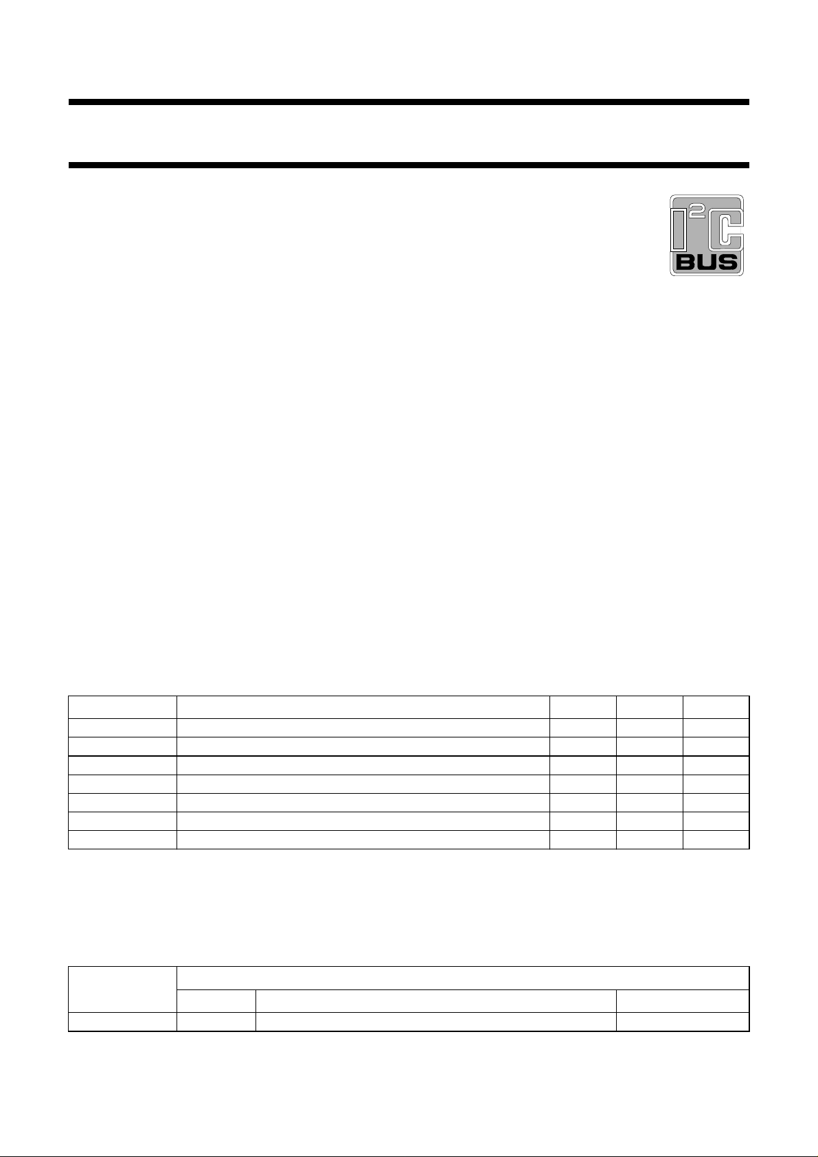
handbook, full pagewidth
BLOCK DIAGRAM
Dolby* Pro Logic Surround;
Incredible Sound
Philips Semiconductors Product specification
I2S input 2
2
I
S_BCKIN1
2
I
S_WSIN1I2S input 1
2
I
S_DATAIN1
2
I
S_DATAIN2
2
I
S_BCKIN2
2
S_WSIN2
I
DSP_RESET
TSCAN
RTCB
22
23
24
25
27
26
17
13
3
DSP_IN1
7
DSP_IN2
2
I
INPUT
SWITCH
CIRCUIT
TEST
FLAG TEST
CONTROL
8
DSP_OUT1
S
9
DSP_OUT2
data 1
10
DOLBY PRO LOGIC
+
SDA
SURROUND
CHANNEL
DELAY LINE
OR
DOLBY 3 STEREO
OR
HALL/MATRIX
OR
INCREDIBLE
SOUND
AUTO BALANCE
FUNCTION
2
C BUS
I
TRANSCEIVER
15
SCL
2
2
S_BCKOUT
I
1
2
I
S_WSOUT
21
OSC
SAA7710T
VARIABLE
OUTPUT
MATRIX
OSCILLATOR
20
XTAL
SHTCB
I2S OUT 1
I2S OUT 2
2
S OUT 3
I
4
28
2
I
S_DATAOUT1
29
2
I
S_DATAOUT2
30
2
I
S_DATAOUT3
5
V
DD1
12
V
+
DD2
32
V
DD3
19
V
DD_XTAL
18
V
SS_XTAL
6
V
SS1
11
V
SS2
31
V
SS3
MGE751
I2S outputs
SAA7710T
S
L
5-BAND
C
PARAMETRIC
EQUALIZER
R
SW
16
OR
TONE
CONTROL
14
A0
Fig.1 Block diagram.
Page 4
Philips Semiconductors Product specification
Dolby* Pro Logic Surround;
Incredible Sound
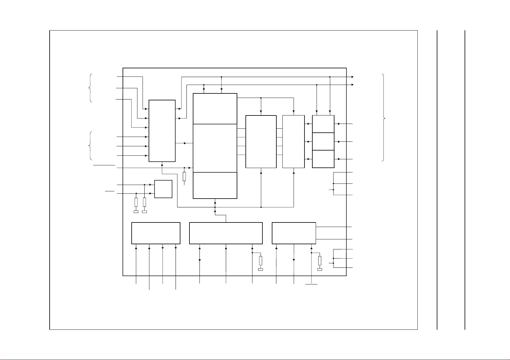
PINNING
SYMBOL PIN DESCRIPTION
2
S_WSOUT 1 I2S-bus slave word-select
I
output
2
I
S_BCKOUT 2 I2S-bus slave bit-clock output
RTCB 3 asynchronous reset test control
block input (active LOW)
SHTCB 4 clock divider switch enable
input (LOW = divide)
V
DD1
V
SS1
DSP_IN1 7 flag input 1
DSP_IN2 8 flag input 2
DSP_OUT1 9 flag output 1
DSP_OUT2 10 flag output 2
V
SS2
V
DD2
TSCAN 13 scan control input
A0 14 I
SDA 15 I
SCL 16 I
DSP_RESET 17 chip reset input (active LOW)
V
SS_XTAL
V
DD_XTAL
XTAL 20 crystal oscillator output
OSC 21 crystal oscillator input
2
I
S_BCKIN1 22 I2S-bus master bit-clock input 1
2
S_WSIN1 23 I2S-bus master word-select
I
2
I
S_DATAIN1 24 I2S-bus master data input 1
2
I
S_DATAIN2 25 I2S-bus master data input 2
2
S_WSIN2 26 I2S-bus master word-select
I
2
I
S_BCKIN2 27 I2S-bus master bit-clock input 2
2
I
S_DAT AOUT1 28 I2S-bus slave data output 1
2
I
S_DATAOUT2 29 I2S-bus slave data output 2
2
S_DATAOUT3 30 I2S-bus slave data output 3
I
V
SS3
V
DD3
5 positive power supply
6 ground power supply
11 ground power supply
12 positive power supply
2
C-bus slave address
selection input
2
C-bus serial data input/output
2
C-bus serial clock input
18 ground power supply crystal
oscillator
19 positive power supply crystal
oscillator
input 1
input 2
31 ground power supply
32 positive power supply
handbook, halfpage
I2S_WSOUT
2
S_BCKOUT
I
DSP_OUT1
DSP_OUT2
1
2
RTCB
3
SHTCB
DSP_IN1
DSP_IN2
TSCAN
V
V
V
V
DD1
SS1
SS2
DD2
A0
SDA
SCL
4
5
6
7
8
SAA7710T
9
10
11
12
13
14
15
16
Fig.2 Pin configuration.
MGE750
SAA7710T
V
32
DD3
V
31
SS3
2
I
S_DATAOUT3
30
2
S_DATAOUT2
I
29
2
S_DATAOUT1
I
28
2
I
S_BCKIN2
27
2
S_WSIN2
I
26
2
S_DATAIN2
I
25
2
S_DATAIN1
I
24
2
S_WSIN1
I
23
2
S_BCKIN1
I
22
OSC
21
XTAL
20
V
19
DD_XTAL
V
18
SS_XTAL
DSP_RESET
17
1998 Mar 13 4
Page 5

Philips Semiconductors Product specification
Dolby* Pro Logic Surround;
Incredible Sound
FUNCTIONAL DESCRIPTION
Figure 1 shows the block diagram of the SAA7710T.
The SAA7710T consists of a Dolby Pro Logic decoder
together with equalizer or tone control. The Dolby Pro
Logic part of the IC may be used to decode audio
soundtracks (Dolby surround movies or Dolby surround
video productions) from for example, a video recorder
(VCR) or a CD laser disc into four channels Left, Centre,
Right and Surround (L, C, R and S).
If desired, post-processing with either an equalizer or a
tone control section is possible. In addition to this, a Sub
Woofer (SW) channel, digital volume control and a
user-programmable variable output matrix are
implemented.
Hall/matrix surround sound functions are implemented for
material not encoded using Dolby Surround. These
features can be used as an alternative to Dolby Pro Logic
and can also be combined with the equalizer or tone
control sections.
Incredible sound is a Philips patented technology which
substantially improves the stereo effect of a television or
audio system. Using advanced signal processing,
speakers that are positioned close together can imitate the
sound produced by speakers that are far apart.
Functional modes
The device thus supports three main modes, Dolby Pro
Logic/Dolby 3 stereo or hall/matrix surround or Incredible
sound mode. All modes can be combined with equalizing
(3-band or 5-band) or tone control depending on f
available cycle budget.
HE DOLBY PRO LOGIC MODE
T
In Dolby Pro Logic mode, several blocks must be initialized
and controlled during operation:
• Noise generator and noise sequencer
• Centre channel mode
(1)
(normal, phantom, wide, off)
• Combining network coefficients
• 7 kHz low-pass filter in surround channel
• Surround channel delay time
(1)
(1)
• Modified Dolby B noise reduction must be on.
Possible post-processing modes for Dolby Pro Logic are:
• Volume control only
(1) The coefficient set used to initialize and control the operation
of the Dolby Pro Logic mode depends upon the selected
sampling frequency f
= 32, 44.1 or48 kHz.
s
and
s
SAA7710T
• Equalizer (3- or 5-band on L, C and R) or tone control
(L, C, R and S); fixed output matrix
• Equalizer (5-band on L, C and R); variable output
(1)
matrix
• Extra sub woofer
HE DOLBY 3 STEREO MODE
T
; volume control
(1)
.
In Dolby 3 stereo mode, several blocks must be initialized
and controlled during operation:
• Noise generator and noise sequencer
• Centre channel mode
(1)
(normal, phantom, wide and off)
• Combining network coefficients
• Incredible Sound widening of the stereo base on two
speakers
• Effect is user adjustable.
HE HALL/MATRIX SURROUND MODE
T
In hall/matrix surround mode, the blocks listed below must
be initialized and controlled during operation:
• Input balance control
• Hall or matrix surround Mode setting
• All-pass and filter transfer characteristics
• 7 kHz low-pass filter in surround channel
• Surround channel delay
(1)
.
Possible post-processing modes for hall/matrix surround
are as above:
• Volume control only
• Equalizer (5-band on L, C and R) or tone control
(L, C, R and S); fixed output matrix
• Equalizer (5-band on L,C,R); variable output matrix
volume control
• Extra sub woofer
T
HE INCREDIBLE SOUND MODE
(1)
.
In the Incredible sound mode the blocks listed below must
be initialized and controlled during operation:
• Incredible sound coefficients
• Combining network coefficients.
Possible post-processing modes for incredible sound are
as follows:
• Volume control only
• Equalizer (5-band on L and R) or tone control (L and R);
variable output matrix
• Extra sub-woofer
(1)
, volume control
(1)
.
(1)
; volume control
(1)
(1)
(1)
; volume control
(1)
;
1998 Mar 13 5
Page 6

Philips Semiconductors Product specification
Dolby* Pro Logic Surround;
Incredible Sound
ADDITIONAL INFORMATION
The possible modes of operation are discussed in more
detail in the
Guide, Application Note AN95063”
which features are available for a given system clock
frequency and sample frequency and the possible input
configurations.
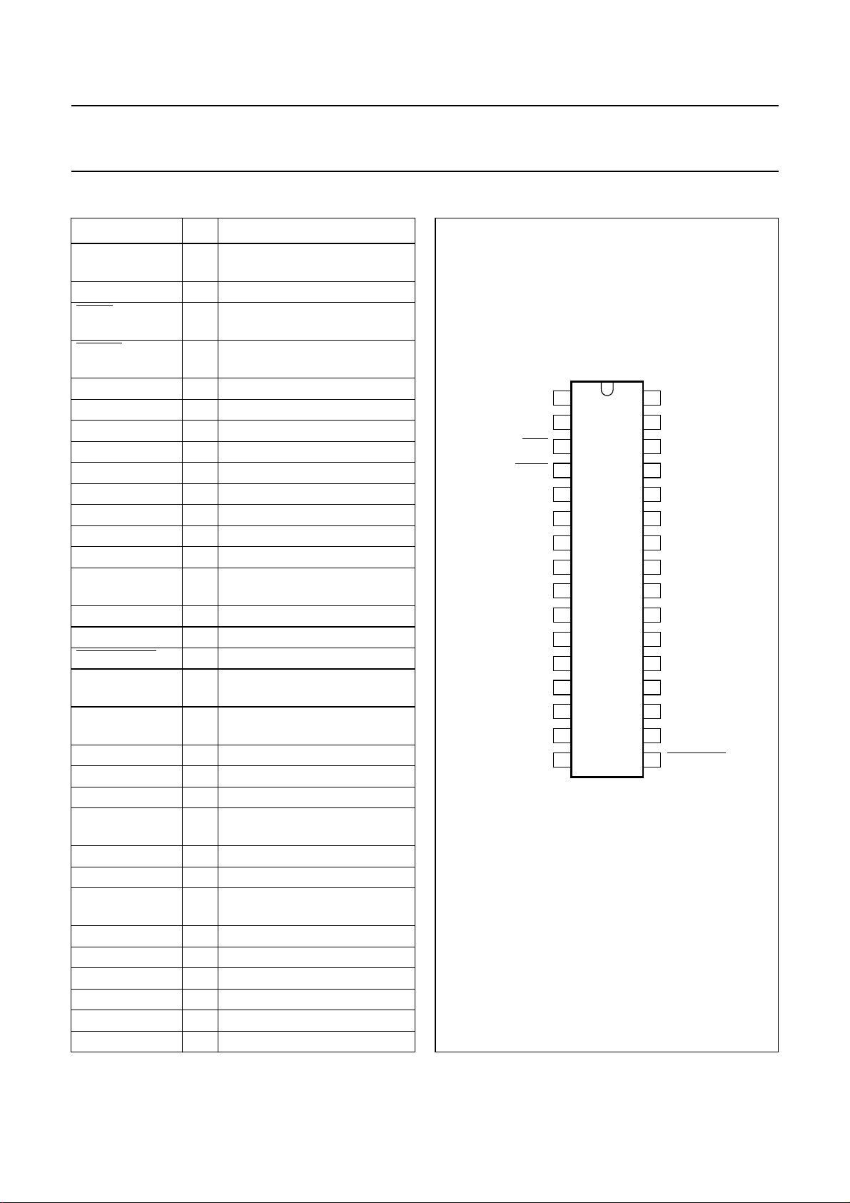
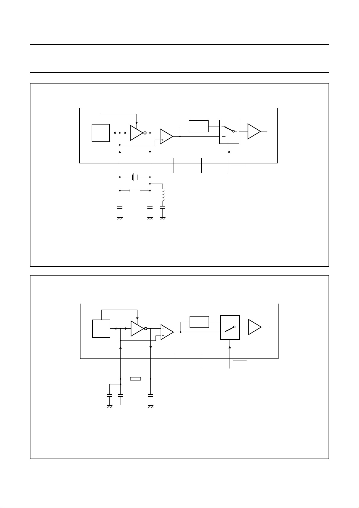
Clock circuit and oscillator
The chip has an on board crystal clock oscillator. The block
schematic of this Pierce oscillator is shown in
Figs 3 and 4. The active element needed to compensate
for the loss resistance of the crystal is the amplifier Gm.
This amplifier is placed between the XTAL (output) pin and
the OSC (sense) pin. The gain of the oscillator is internally
controlled by the automatic gain control. This prevents too
much power loss in the crystal. The higher harmonics are
then as low as possible. The signals on the OSC and XTAL
pin are differentially amplified.
The oscillator has these two modes of operation:
The crystal oscillator mode: in this mode (see Fig.3),
a quartz crystal oscillator is used to generate a clock
signal which is subsequently divided by 2 to ensure that
the final clock signal has a 50% duty cycle.
The oscillator circuit components R
depend on the crystal. In the case of an overtone
oscillator, the ground harmonic is filtered out by L1 and
C3. Pin SHTCB is held low so that the divided signal is
selected. Only a quartz crystal should be used in this
mode.
“SAA7710T Dolby Pro Logic Programming
. This also includes
and C1, C2
bias
SAA7710T
The slave oscillator mode: in this mode (see Fig.4),
the oscillator circuit acts as a slave driven by a master
system clock. The clock divider can be switched on or off
using pin
cycle of the clock will depend on the master system
clock duty cycle and the rising and falling edge times.
This places a tolerance of 5% on the 50% duty cycle of
the master system clock (see Chapter “AC
characteristics”).
In order to be able to control the phase of the clock signal
during testing the divider is skipped and the signal is
directly fed to the circuit via the multiplexer in the TEST
position.
S
UPPLY OF THE CRYSTAL OSCILLATOR
The power supply connections to the oscillator are
separated from the other supply lines to minimise
feedback from on-chip ground bounce to the oscillator
circuit. Noise on the power supply affects the AGC
operation so the power supply should be decoupled.
The V
V
DD_XTAL
SHTCB. When the divider is not used, the duty
SS_XTAL
pin is used as ground supply and the
as positive supply.
1998 Mar 13 6
Page 7
Philips Semiconductors Product specification
Dolby* Pro Logic Surround;
Incredible Sound
handbook, full pagewidth
AGC
ON CHIP
OFF CHIP
C1
10 pF
21
OSC
Gm
100 kΩ
R
bias
10 pF
C2
XTAL
DIVIDE
BY 2
V
DD_XTALVSS_XTAL
L1
4.7 µH
C3
1 nF
SAA7710T
CLOCK
4181920
SHTCB
BUFFER
MGE752
0
1
TEST
= 0
handbook, full pagewidth
AGC
ON CHIP
OFF CHIP
40 pF
Fig.3 Block diagram crystal oscillator circuit.
DIVIDE
BY 2
DD_XTALVSS_XTAL
slave
input
21
OSC
10 pF
Gm
100 kΩ
XTAL
10 nF
V
CLOCK
4181920
SHTCB
BUFFER
MGE753
0
1
TEST
= 1
Fig.4 Block diagram slave oscillator circuit.
1998 Mar 13 7
Page 8
Philips Semiconductors Product specification
Dolby* Pro Logic Surround;
Incredible Sound
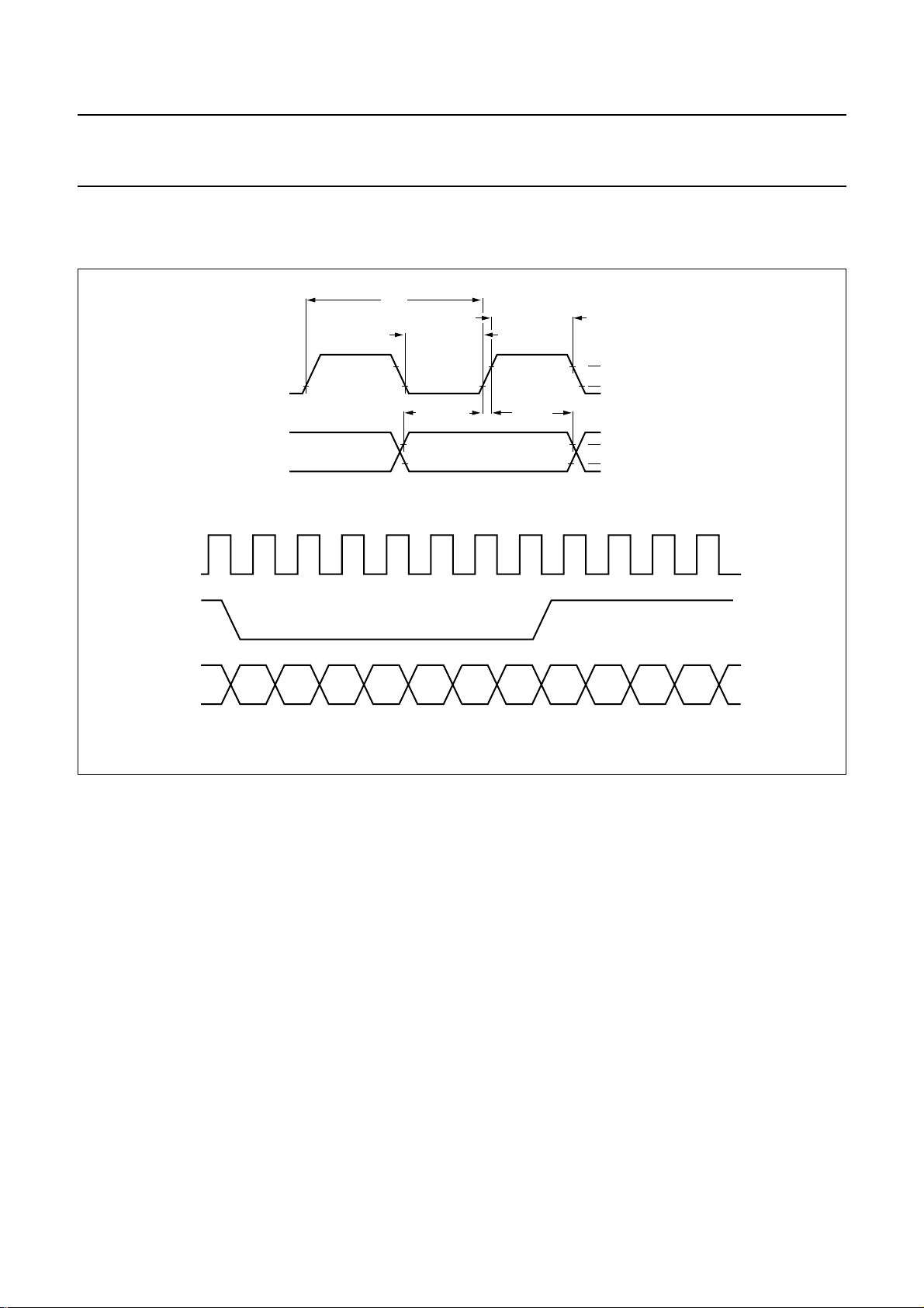
I2S-bus Interfaces and system clock
2
S-BUS BASICS
I
handbook, full pagewidth
SCK
SD
WS
SCK
T
cy
tLC≥0.35 T
tsr≥0.2 T thr≥0
SAA7710T
tHC≥0.35 T
VIH (70%)
VIL (20%)
VIH (70%)
VIL (20%)
WS
SD
MSB
LEFT
Fig.5 I2S-bus timing and format.
For communication with external digital sources and or
additional external processors the I2S-bus digital interface
bus is used. It is a serial 3-line bus, with one line for data,
one line for clock and one line for the word select.
Figure 5 shows an excerpt of the Philips I2S-bus
specification interface report regarding the general timing
and format of I2S-bus. Word Select (WS) logic 0 means left
channel word, logic 1 means right channel word.
The serial data is transmitted in two’s complement with the
MSB first. One clock period after the negative edge of the
word select line the MSB of the left channel is transmitted.
Data is synchronised with the negative edge of the clock
and latched at the positive edge.
MSB
RIGHT
MBH173
2
S-BUS INPUT CIRCUIT
I
The I2S-bus input circuits can be configured in the
following way using the SEL-IN1/IN2 bit (see Table 4):
1. I2S input 1 is master
(SEL-IN1/IN2 bit = logic 0(default))
2. I2S input 2 is master (SEL-IN1/IN2 bit = logic 1).
The incoming bit-clock frequency defines the accuracy in
terms of number of bits of the incoming data samples.
The input circuit is designed to accept any number of bits
per channel up to a maximum of 18 bits. The accepted
data format is MSB-first.
1998 Mar 13 8
Page 9
Philips Semiconductors Product specification
Dolby* Pro Logic Surround;
Incredible Sound
Table 1 Data Accuracy in I2S-bus Interface
INCOMING DATA WIDTH I2S-BUS IN DATA WIDTH I2S-BUS OUT DATA WIDTH
A<18 A A
B≥18 18 18
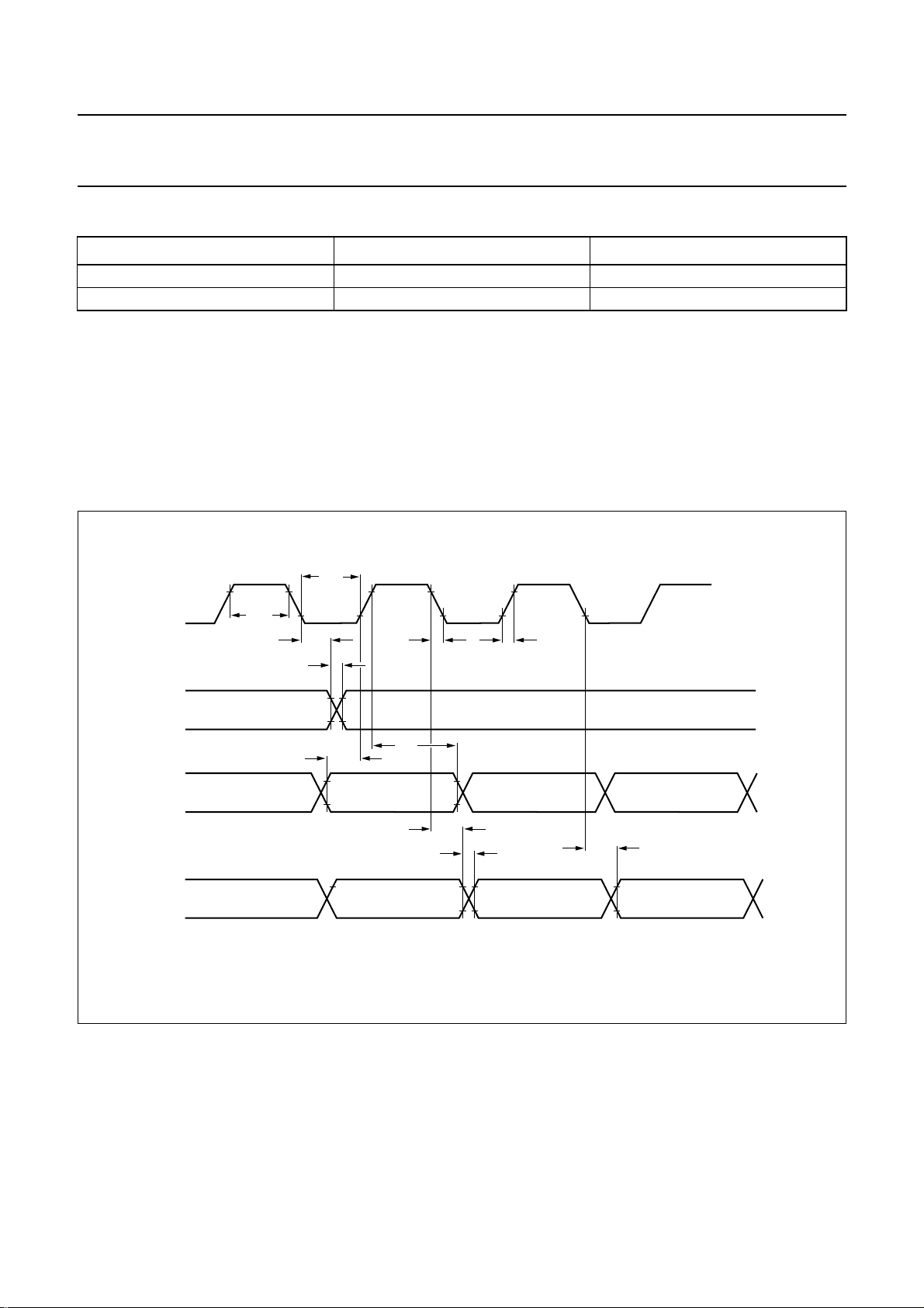
THE I2S-BUS OUTPUT INTERFACE
The I2S-bus data output interfaces (see Fig.1) I2S OUT 1,
I2S OUT 2 and I2S OUT 3 use the same I2S-bus data
signals which are selected by the input switch circuit. The
I2S-bus WS and BCK output signals remain in phase with
the external input signals at all times. The output data is
1/fs cycle delayed relative to the input data. The selected
word-select and bit-clock are included as part of the output
handbook, full pagewidth
CL
WS
t
HC
t
LC
t
d1
t
r
t
f
t
interface: I
signals can be 3-stated by setting the DIS_BCKWS bit
(see Table 4). The 3-state output of the I2S_DATAOUT3
signal can be enabled by setting the ENA_I2S3 bit (see
Table 4).
The timing diagram of the I2S-bus outputs is shown in
Fig.6. The timing details can be found in Chapter “AC
characteristics”.
f
2
S_WSOUT, I2S_BCKOUT. These two output
2
I
S_BCKIN1, 2
2
I
S_BCKOUT
t
r
2
S_WSIN1, 2
I
2
I
S_WSOUT
SAA7710T
DATA (in)
DATA (out)
t
t
s2
d2
DATA VALID
MSB
t
d3
t
r
t
f
MSB
t
acc
Fig.6 Timing diagram of I2S-bus output interface.
2
I
S_DATAIN1, 2
2
I
S_DATAOUT1, 2, 3
MGE755
1998 Mar 13 9
Page 10

Philips Semiconductors Product specification
Dolby* Pro Logic Surround;
Incredible Sound
I2C-bus control and commands
HARACTERISTICS OF THE I
C
The I2C-bus is for 2-way, 2-line communication between
different ICs or modules. The two lines are a serial data
line (SDA) and a serial clock line (SCL). Both lines must be
connected to the V
connected to the output stages of a microprocessor.
Data transfer can only be initiated when the bus is not
busy.
B
IT TRANSFER
One data bit is transferred during each clock pulse.
The data on the SDA line must remain stable during the
HIGH period of the clock pulse as changes in the data line
at this time will be interpreted as control signals.
The maximum clock frequency is 100 kHz (see Fig.7).
START
AND STOP CONDITIONS
Both data and clock lines remain HIGH when the bus is not
busy. A HIGH-to-LOW transition of the data line, while the
clock is HIGH is defined as the START condition (S).
A LOW-to-HIGH transition of the data line while the clock
is HIGH is defined as the STOP condition (P) (see Fig.8).
2
C-BUS
via a pull-up resistor when
DDX
SAA7710T
ATA TRANSFER
D
A device generating a message is a ‘transmitter’, a device
receiving a message is the ‘receiver’. The device that
controls the message is the ‘master’ and the devices which
are controlled by the master are the ‘slaves’ (see Fig.9).
A
CKNOWLEDGE
The number of data bytes transferred between the START
and STOP conditions from transmitter to receiver is not
limited. Each byte of eight bits is followed by one
acknowledge bit. The acknowledge bit is a HIGH level put
on the bus by the transmitter whereas the master
generates an extra acknowledge related clock pulse.
A slave receiver which is addressed must generate an
acknowledge after the reception of each byte. Also a
master must generate an acknowledge after the reception
of each byte that has been clocked out of the slave
transmitter. The device that acknowledges has to pull
down the SDA line during the acknowledge clock pulse, so
that the SDA line is stable LOW during the HIGH period of
the acknowledge related clock pulse, set up and hold times
must be taken into account. A master receiver must signal
an end of data to the transmitter by not generating an
acknowledge on the last byte that has been clocked out of
the slave. In this event the transmitter must leave the data
line HIGH to enable the master to generate a STOP
condition (see Fig.10).
handbook, full pagewidth
SDA
SCL
data line
stable
data valid
change
of data
allowed
Fig.7 Bit transfer on the I2C-bus.
1998 Mar 13 10
MLC160
Page 11

Philips Semiconductors Product specification
Dolby* Pro Logic Surround;
Incredible Sound
ndbook, full pagewidth
SDA
SCL
S P
START condition STOP condition
SAA7710T
MLC161
Fig.8 START and STOP conditions.
handbook, full pagewidth
SDA
MSB
SCL
S P
START condition STOP condition
1 2 7 8 9 1 2 3 to 8 9
acknowledgement
signal from receiver
ACK
byte complete
interrupt within receiver
clock line held LOW while
interrupts are serviced
acknowledgement
signal from receiver
MLC162
Fig.9 Data transfer on the I2C-bus.
1998 Mar 13 11
Page 12

Philips Semiconductors Product specification
Dolby* Pro Logic Surround;
Incredible Sound
handbook, full pagewidth
data output
from transmitter
data output
from receiver
SCL from
master
S
START condition
SAA7710T
not acknowledge
acknowledge
12 789
MLC163
clock pulse for
acknowledgement
Fig.10 Acknowledge on the I2C-bus.
I2C-BUS FORMAT
Addressing
Before any data is transmitted on the I2C-bus, the device
which should respond is addressed first. The addressing is
always done with the first byte transmitted after the START
procedure.
Slave address (pin A0)
The chip acts as a slave receiver or a slave transmitter.
Therefore the clock signal SCL is only an input signal.
The data signal SDA is a bidirectional line. The chip slave
address is shown in Table 2.
The sub address bit A0 corresponds to the hardware
address pin A0 which allows the device to have 1 of 2
different addresses.
Write cycles
The I2C-bus configuration for a write cycle is shown in
Fig 12. The write cycle is used to write in the input selector
control register and to initialise or update coefficient
values.
The data length is 2 bytes or 3 bytes depending of the
accessed memory. If the Y-memory is addressed the data
length is 2 bytes, in case of the X-memory the length is
3 bytes. The slave receiver detects the address and
adjusts the bytes accordingly.
Read cycles
The I2C-bus configuration for a Read cycle is shown in
Fig 13. The read cycle is used to read data values from
XRAM or YRAM.
1998 Mar 13 12
Page 13

Philips Semiconductors Product specification
Dolby* Pro Logic Surround;
Incredible Sound
I2C-BUS FUNCTION BITS
Input selector control register
The write only, two byte, input selector control register is
located on absolute address 0FFFH (4095) and consists
of 16 bits, starting with bit 0 and ending with bit 15.
Deviation from the I2C-bus specification
1. The data hold time (t
stated in the I2C-bus specification) should be as
follows:
a) For the crystal oscillator mode (
6
≥
---------
f
xtal
b) For the slave oscillator mode (SHTCB= 0):
6
≥
-------------
f
slave
c) For the slave oscillator mode (SHTCB = 1):
3
≥
-------------
f
slave
) for this device (≥0 ns as
HD;DAT
SHTCB = 0):
SAA7710T
During the write cycle, the I
be reduced.
The I2C-bus clock frequency has the following constraints:
fs> 2 × f
IIC
fs=I2S-bus sampling frequency
f
=I2C-bus clock frequency.
IIC
If this constraint cannot be met, a higher I2C-bus frequency
can be obtained in the following way:
By making the I2C-bus master insert a delay (td) after the
acknowledge pulse (see Fig.11). The delay should be
larger than or equal to 1/fs where fs is the I2S-bus
sampling frequency.
By not using the auto-increment feature. This means
that each data word must be preceded by its intended
destination address.
2
C-bus clock frequency must
handbook, full pagewidth
SCL
SDA
auto-increment address register
ACKNOWLEDGE AFTER WORD
Fig.11 Timing of reduced I2C-bus frequency.
1998 Mar 13 13
t
d
MGE756
Page 14

Philips Semiconductors Product specification
Dolby* Pro Logic Surround;
SAA7710T
Incredible Sound
Table 2 Slave address
MSB LSB
001111A0R/
2
Table 3 Location of input selector control register bits in I
MSB LSB
DATAH DATAL
15141312111098A76543210AP
Note
1. Explanation for the contents of the register bits:
2
a) A= standard I
b) Number= bit number according to Table 4.
c) P = standard I2C-bus STOP condition.
Table 4 Input selector control bits
SYMBOL FUNCTION NUMBER OF BITS ON RESET BIT NO
SEL-IN1/IN2 I
DIS_BCKWS disable I
2
ENA-I
S3 enable I2S_DATAOUT3 1 disable(0) 13
IMODE I flag resets/background tasking 1 resets(0) 15
C-bus acknowledge.
2
S input 1 or I2S input 2 input 1 IN1(0) 5
2
S_BCKOUT and I2S_WSOUT 1 enable(0) 7
C-bus serial transmission; note 1
W
XRAM format
The XRAM block consists of 256 18-bit RAM locations 0 to 255 and is located on the absolute address range of 0000H
to 00FFH. The I2C-bus transfer consists of 18 useful bits out of 24 bits.
Table 5 Format XRAM bits; note 1
MSB LSB
DATAH DATAM DATAL
DDDDDD1716A1514131211109 8A76543210AP
Note
1. Explanation for the contents of the register bits:
a) D= contents of I2C-bus data register bit is don’t care.
b) A= standard I2C-bus acknowledge.
c) Number = bit number being useful bit XRAM memory.
d) P= standard I2C-bus STOP condition.
1998 Mar 13 14
Page 15

Philips Semiconductors Product specification
Dolby* Pro Logic Surround;
SAA7710T
Incredible Sound
YRAM format
The YRAM block consists of 256 12-bit RAM locations 0 to 255 and is located on the absolute address range of
0800H to 08FFH. The I2C-bus transfer consists of 12 useful bits out of 16 bits.
Table 6 Format YRAM bits; note 1
MSB LSB
DATAH DATAM
DDDD111098A76543210AP
Note
1. Explanation for the contents of the register bits:
a) D= contents of I
b) A= standard I2C-bus acknowledge.
c) Number = bit number being useful bit XRAM memory.
d) P= standard I2C-bus STOP condition.
Error processing
2
C-bus data register bit is don’t care.
If a read action is done without first initialising the memory address the acknowledge after the read command will not be
generated by the chip. This should be treated as an error message:
Table 7
S Write ACK ADDRH ACK ADDRL ACK S Read Correct read sequence
S Read NEG ACK Incorrect read sequence; address is not initialized
1998 Mar 13 15
Page 16

This text is here in white to force landscape pages to be rotated correctly when browsing through the pdf in the Acrobat reader.This text is here in
_white to force landscape pages to be rotated correctly when browsing through the pdf in the Acrobat reader.This text is here inThis text is here in
white to force landscape pages to be rotated correctly when browsing through the pdf in the Acrobat reader. white to force landscape pages to be ...
1998 Mar 13 16
Philips Semiconductors Product specification
Dolby* Pro Logic Surround;
Incredible Sound
A
C
K
R/W
A
C
K
01111A00
0 ADDR H ADDR L DATA H DATA M
S
address
A
C
K
A
C
K
auto increment if repeated n-groups of 3 (2) bytes
Fig.12 Master transmitter writes to chip.
A
C
K
R/W
A
C
K
01111A00
0 011 111A
S
address
A
0ADDR H ADDR L DATA H
C
S
K
0
R/W
A
C
K
auto increment if repeated n-groups of 3 (2) bytes
A
C
K
A
DATA M DATA L
C
K
A
C
DATA L
A
C
K
K
MBH529
A
C
K
MBH528
P
P
Fig.13 Master transmitter reads from chip.
SAA7710T
Page 17

Philips Semiconductors Product specification
Dolby* Pro Logic Surround;
SAA7710T
Incredible Sound
DSP_RESET
The DSP_RESET pin is active LOW and has an internal
pull-up resistor. To enable a proper switch-on of the supply
voltage a capacitor should be connected between this pin
and VSS. The capacitor value is such that the chip is in a
reset state as long as the power supply is not stabilized.
The DSP_RESET has the following functions:
• The bits of the input selector control register are set to
When the level on the
program starts to run.
When the level on theDSP_RESET pin is low, the SDA pin
is asynchronously set to a high-impedance state. In the
absence of a clock and during the power-up reset, the SDA
line is high-impedance.
EST MODE CONNECTIONS (TSCAN, RTCB AND SHTCB
T
PINS)
logic 0 (see Table 4)
• The program counter is set to address 0000H
2
• The I
C-bus interface is initialised; the SDA pin is
guaranteed high-impedance.
The TSCAN, RTCB and SHTCB pins are used to put the
chip in test mode and to test the internal connections.
Each pin has an internal pull-down resistor to ground.
In the application these pins can be left open-circuit or
connected to ground.
LIMITING VALUES
In accordance with the Absolute Maximum Rating System (IEC134).
SYMBOL PARAMETER CONDITIONS MIN. MAX. UNIT
V
∆V
V
l
IK
DD
DD
i(max)
DC supply voltage −0.5 +6.5 V
voltage difference between two V
pins − 550 mV
DDx
maximum input voltage −0.5 VDD+ 0.5 V
DC input clamp diode current Vi< −0.5 V or
Vi>VDD+ 0.5 V
l
l
OK
O
DC output clamp diode current output
type 4 mA
DC output source or sink current output
Vo< −0.5 V or
Vo>VDD+ 0.5 V
−0.5V<Vo<VDD+ 0.5 V − 20 mA
type 4 mA
l
DD
DC output source or sink current output
−0.5V<Vo<VDD+ 0.5 V − 20 mA
type 4 mA
l
l
V
DD
SS
ESD
DC VDD supply current per pin − 50 mA
DC VSS supply current per pin − 50 mA
ESD sensitivity for all pins
human body model 100 pF; 1500 Ω 3000 − V
machine model all pins except pin OSC 200 pF; 2.5 µH; 0 Ω 300 − V
machine model pin OSC 200 pF; 2.5 µH; 0 Ω 250 − V
LTCH latch-up protection CIC spec/test method 100 − mA
P
tot
T
amb
T
stg
total power dissipation − 700 mW
operating ambient temperature −40 +85 °C
storage temperature −65 +150 °C
DSP_RESET pin is HIGH, the DSP
− 10 mA
− 20 mA
THERMAL CHARACTERISTICS
SYMBOL PARAMETER VALUE UNIT
R
th j-a
thermal resistance from junction to ambient in free air 57 K/W
1998 Mar 13 17
Page 18

Philips Semiconductors Product specification
Dolby* Pro Logic Surround;
SAA7710T
Incredible Sound
DC CHARACTERISTICS
V
DD1=VDD2=VDD3=VDD_XTAL
SYMBOL PARAMETER CONDITIONS MIN. TYP. MAX. UNIT
V
DDtot
I
DD(tot)
P
tot
V
IH
total DC supply voltage 4.5 5 5.5 V
total DC supply current DSP frequency = 18 MHz;
total power dissipation DSP frequency = 18 MHz;
HIGH level input voltage
all digital inputs and I/Os
V
IL
LOW level input voltage
all digital inputs and I/Os
V
hys
V
OH
hysteresis voltage pin type I4 − 0.33V
HIGH level output voltage
digital outputs
V
OL
LOW level output voltage
digital outputs
input leakage current Vi= 0 or V
I
LI
I
output leakage current
LO
3-state outputs
R
pu(VDDX)(int)
R
pd(VSSD)(int)
internal pull-up resistor to
V
DDX
internal pull-down resistor
to V
SSD
Crystal oscillator
V
DDX
positive supply voltage
crystal oscillator
= 4.5 to 5.5 V; T
maximum activity DSP
maximum activity DSP
pin types I1, I2 and I3 0.7V
pin type I4 0.8V
pin types I1, I2 and I3 −−0.3V
pin type I4 −−0.2V
V
DDX
pin type O1 and O2
V
DDX
pin types I3, O1 and O2
pin type I1
Vo= 0 or V
pin type I3 and O2
pin type I4 17 − 134 kΩ
pin type I2 17 − 134 kΩ
= −40 to +85 °C; note 1; unless otherwise specified.
amb
− 50 55 mA
− 250 300 mW
−−V
DDX
−−V
DDX
DDX
= 4.5 V; Io= −4 mA;
= 4.5 V; Io= 4 mA;
voltage;
DDX
voltage;
DDX
4.0 −−V
−−0.5 V
−−1µA
−−5µA
4.5 5 5.5 V
DDX
DDX
− V
V
V
Note
1. V
DDX=VDD_XTAL
.
1998 Mar 13 18
Page 19

Philips Semiconductors Product specification
Dolby* Pro Logic Surround;
SAA7710T
Incredible Sound
AC CHARACTERISTICS
V
DD1=VDD2=VDD3=VDD_XTAL
SYMBOL PARAMETER CONDITIONS MIN. TYP. MAX. UNIT
f
xtal
α
f
I
xtal
g
m(XTAL)
V
xtal
C
L(XTAL)
R
xtal
crystal frequency see Fig.3 −−36.864 MHz
spurious frequency attenuation 20 −− dB
current through crystal at input voltage swing 0.2 V − 500 −µA
transconductance at start-up 4 8 − mS
voltage across crystal note 1 − 500 − mV
load capacitance − 25 − pF
allowed loss resistor of crystal Cp= 5 pF; C1 = 10 pF;
Slave oscillator
f
slave
slave frequency no divider; see Fig.4 −−18.432 MHz
SLVOLT slave drive voltage see Fig.4 3.75 −− V
t
r
t
f
input rise times 0.1 to 0.9V
input fall times 0.1 to 0.9V
Timing
2
I
C-BUS INPUTS/OUTPUT
t
f
f
i(max)
2
S-BUS INPUTS/OUTPUTS
I
t
r
t
f
t
HC
t
LC
t
d1
t
d2
t
s2
t
d3
t
acc
ALL OTHER OUTPUTS (O1)
t
r
t
f
ALL OTHER INPUTS
t
r
t
f
fall time I2C-bus 0.1 to 0.9V
maximum input frequency SDA, SCL −−100 kHz
rise time I2S-bus (O2) CL= 30 pF; 0.1 to 0.9V
fall time I2S-bus (O2) CL= 30 pF; 0.1 to 0.9V
CL pulse width HIGH 112 −− ns
CL pulse width LOW 112 −− ns
WS out delay time 0 −− ns
data in hold time 0 −− ns
data in set-up time 25 −− ns
data out delay time 0 − 5ns
data out access time −−5 + 0.5 × C
rise time CL= 30 pF; 0.1 to 0.9V
fall time CL= 30 pF; 0.1 to 0.9V
input rise times VDD= 5.5 V − 6 200 ns
input fall times VDD= 5.5 V − 6 200 ns
= 4.5 to 5.5 V; T
C2 = 10 pF
=25°C; unless otherwise specified.
amb
DD_XTAL
DD_XTAL
DD
; note 2 −−20 ns
; note 2 −−20 ns
DD
DD
DD
DD
− 20 60 Ω
− 5.7 − ns
− 7.3 − ns
− 8.3 − ns
(3)
ns
L
− 7.3 − ns
− 8.3 − ns
Notes
1. The load capacitance is the sum of the series connection of C1 and C2 (see Fig.3) and the parasitic parallel capacitor
of the crystal C
.
p
2. With a 50%, ±5% duty cycle on oscillator drive input (see Fig.4).
3. The value for the capitative load CL is given in pF.
1998 Mar 13 19
Page 20

Philips Semiconductors Product specification
Dolby* Pro Logic Surround;
Incredible Sound
INTERNAL CIRCUITRY
PIN SYMBOL PIN TYPE
7 DSP_IN1 I1
8 DSP_IN2 I1
16 SCL I1
2
22 I
23 I
24 I
25 I
26 I
27 I
17
S_BCKIN1 I1
2
S_WSIN1 I1
2
S_DATAIN1 I1
2
S_DATAIN2 I1
2
S_WSIN2 I1
2
S_BCKIN2 I1
DSP_RESET I4
DC VOL T AGE
(V)
SAA7710T
INTERNAL CIRCUIT
7, 8, 16, 22, 23,
24, 25, 26, 27
MGE758
RTCB I2
3
4
SHTCB I2
13 TSCAN I2
14 A0 I1
2
1I
S_WSOUT O2
2
2I
S_BCKOUT O2
9 DSP_OUT1 O2
2
30 I
S_DATAOUT3 O2
17
+
MGE759
3, 4, 13, 14
MGE760
1, 2, 9, 30
MGE761
1998 Mar 13 20
Page 21

Philips Semiconductors Product specification
Dolby* Pro Logic Surround;
Incredible Sound
PIN SYMBOL PIN TYPE
15 SDA I3
10 DSP_OUT2 O1
2
28 I
29 I
12 V
31 V
32 V
S_DATAOUT1 O1
2
S_DATAOUT2 O1
5V
DD1
6V
SS1
11 V
SS2
DD2
SS3
DD3
21 OSC tbf
20 XTAL tbf
19 V
18 V
DD_XTAL
SS_XTAL
DC VOL T AGE
(V)
tbf
0
0
5
0
5
5
0
SAA7710T
INTERNAL CIRCUIT
15
MGE762
10, 28, 29
MGE763
19
20
21
1998 Mar 13 21
18
MGE764
Page 22

This text is here in white to force landscape pages to be rotated correctly when browsing through the pdf in the Acrobat reader.This text is here in
_white to force landscape pages to be rotated correctly when browsing through the pdf in the Acrobat reader.This text is here inThis text is here in
white to force landscape pages to be rotated correctly when browsing through the pdf in the Acrobat reader. white to force landscape pages to be ...
1998 Mar 13 22
handbook, full pagewidth
APPLICATION INFORMATION
Philips Semiconductors Product specification
Dolby* Pro Logic Surround;
Incredible Sound
2
I
S input 1
I2S input 2
220 Ω 220 Ω
220 pF
220 Ω 220 Ω
220 pF
220 Ω 220 Ω
220 pF
220 Ω 220 Ω
220 pF
220 Ω 220 Ω
220 pF
220 Ω 220 Ω
220 pF
470 pF
2
I
S_BCKIN1
2
S_WSIN1
I
2
S_DATAIN1
I
2
I
S_DATAIN2
2
S_BCKIN2
I
2
I
S_WSIN2
DSP_RESET
TSCAN
RTCB
22
23
SAA7710T
VARIABLE
OUTPUT
MATRIX
OSCILLATOR
21
OSC
100 kΩ
10
pF
20
XTAL
4.7 µH
10
pF
I2S OUT 1
I2S OUT 2
I2S OUT 3
4
SHTCB
1
nF
+
MGE757
I2C BUS
Ω
16
SCL
+5 V
S
L
C
R
SW
10
kΩ
100
pF
5-BAND
PARAMETRIC
EQUALIZER
OR
TONE
CONTROL
14
A0
24
25
I2S
INPUT
DSP_IN1
7
DSP_IN2
SWITCH
CIRCUIT
TEST
FLAG TEST
CONTROL
8
DSP_OUT1
data 1
9
DSP_OUT2
+
10
27
26
17
13
3
SURROUND
CHANNEL
DELAY LINE
DOLBY PRO LOGIC
DOLBY 3 STEREO
HALL/MATRIX
INCREDIBLE
SOUND
AUTO BALANCE
FUNCTION
15
SDA
220
10
Ω
kΩ
+5 V
OR
OR
OR
TRANSCEIVER
220
100
pF
2
I
2
2
I
1
2
28
I
2
29
I
2
I
30
V
5
V
12
V
32
V
19
V
18
V
6
V
11
V
31
S_BCKOUT
S_WSOUT
S_DATAOUT1
S_DATAOUT2
S_DATAOUT3
DD1
DD2
DD3
DD_XTAL
SS_XTAL
SS1
SS2
SS3
220 Ω 220 Ω
220 Ω 220 Ω
220 Ω 220 Ω
220 Ω 220 Ω
220 Ω 220 Ω
100
nF
100
nF
100
nF
100
nF
BLM32A07
100 µF
(6.3 V)
BLM32A07
100 µF
(6.3 V)
220 pF
220 pF
220 pF
220 pF
220 pF
+5 V
+5 V
2
S outputs
I
SAA7710T
Fig.14 Application diagram.
Page 23

Philips Semiconductors Product specification
Dolby* Pro Logic Surround;
Incredible Sound
PACKAGE OUTLINE
SO32: plastic small outline package; 32 leads; body width 7.5 mm
D
y
Z
32
17
SAA7710T
SOT287-1
E
c
H
E
A
X
v M
A
pin 1 index
1
e
0 5 10 mm
DIMENSIONS (inch dimensions are derived from the original mm dimensions)
mm
A
A1A2A3b
max.
0.3
2.65
0.1
0.012
0.10
0.004
2.45
2.25
0.096
0.086
0.25
0.01
0.49
0.36
0.02
0.01
p
0.27
0.18
0.011
0.007
UNIT
inches
Note
1. Plastic or metal protrusions of 0.15 mm maximum per side are not included.
(1)E(1)
cD
20.7
20.3
0.81
0.80
7.6
7.4
0.30
0.29
16
b
p
scale
eHELLpQZywv θ
1.27
0.050
10.65
10.00
0.419
0.394
w M
1.4
0.055
A
2
1.1
0.4
0.043
0.016
Q
A
1
detail X
1.2
0.25
1.0
0.047
0.039
(A )
L
p
L
0.25 0.1
0.004
0.010.01
A
3
θ
(1)
0.95
0.55
0.037
0.022
o
8
o
0
OUTLINE
VERSION
SOT287-1
IEC JEDEC EIAJ
REFERENCES
1998 Mar 13 23
EUROPEAN
PROJECTION
ISSUE DATE
95-01-25
97-05-22
Page 24

Philips Semiconductors Product specification
Dolby* Pro Logic Surround;
Incredible Sound
SOLDERING
Introduction
There is no soldering method that is ideal for all IC
packages. Wave soldering is often preferred when
through-hole and surface mounted components are mixed
on one printed-circuit board. However, wave soldering is
not always suitable for surface mounted ICs, or for
printed-circuits with high population densities. In these
situations reflow soldering is often used.
This text gives a very brief insight to a complex technology.
A more in-depth account of soldering ICs can be found in
our
“IC Package Databook”
Reflow soldering
Reflow soldering techniques are suitable for all SO
packages.
Reflow soldering requires solder paste (a suspension of
fine solder particles, flux and binding agent) to be applied
to the printed-circuit board by screen printing, stencilling or
pressure-syringe dispensing before package placement.
Several techniques exist for reflowing; for example,
thermal conduction by heated belt. Dwell times vary
between 50 and 300 seconds depending on heating
method. Typical reflow temperatures range from
215 to 250 °C.
Preheating is necessary to dry the paste and evaporate
the binding agent. Preheating duration: 45 minutes at
45 °C.
(order code 9398 652 90011).
SAA7710T
Wave soldering
Wave soldering techniques can be used for all SO
packages if the following conditions are observed:
• A double-wave (a turbulent wave with high upward
pressure followed by a smooth laminar wave) soldering
technique should be used.
• The longitudinal axis of the package footprint must be
parallel to the solder flow.
• The package footprint must incorporate solder thieves at
the downstream end.
During placement and before soldering, the package must
be fixed with a droplet of adhesive. The adhesive can be
applied by screen printing, pin transfer or syringe
dispensing. The package can be soldered after the
adhesive is cured.
Maximum permissible solder temperature is 260 °C, and
maximum duration of package immersion in solder is
10 seconds, if cooled to less than 150 °C within
6 seconds. Typical dwell time is 4 seconds at 250 °C.
A mildly-activated flux will eliminate the need for removal
of corrosive residues in most applications.
Repairing soldered joints
Fix the component by first soldering two diagonallyopposite end leads. Use only a low voltage soldering iron
(less than 24 V) applied to the flat part of the lead. Contact
time must be limited to 10 seconds at up to 300 °C. When
using a dedicated tool, all other leads can be soldered in
one operation within 2 to 5 seconds between
270 and 320 °C.
1998 Mar 13 24
Page 25

Philips Semiconductors Product specification
Dolby* Pro Logic Surround;
SAA7710T
Incredible Sound
DEFINITIONS
Data sheet status
Objective specification This data sheet contains target or goal specifications for product development.
Preliminary specification This data sheet contains preliminary data; supplementary data may be published later.
Product specification This data sheet contains final product specifications.
Limiting values
Limiting values given are in accordance with the Absolute Maximum Rating System (IEC 134). Stress above one or
more of the limiting values may cause permanent damage to the device. These are stress ratings only and operation
of the device at these or at any other conditions above those given in the Characteristics sections of the specification
is not implied. Exposure to limiting values for extended periods may affect device reliability.
Application information
Where application information is given, it is advisory and does not form part of the specification.
LIFE SUPPORT APPLICATIONS
These products are not designed for use in life support appliances, devices, or systems where malfunction of these
products can reasonably be expected to result in personal injury. Philips customers using or selling these products for
use in such applications do so at their own risk and agree to fully indemnify Philips for any damages resulting from such
improper use or sale.
PURCHASE OF PHILIPS I
Purchase of Philips I
components in the I2C system provided the system conforms to the I2C specification defined by
Philips. This specification can be ordered using the code 9398 393 40011.
2
C COMPONENTS
2
C components conveys a license under the Philips’ I2C patent to use the
1998 Mar 13 25
Page 26

Philips Semiconductors Product specification
Dolby* Pro Logic Surround;
Incredible Sound
SAA7710T
NOTES
1998 Mar 13 26
Page 27

Philips Semiconductors Product specification
Dolby* Pro Logic Surround;
Incredible Sound
SAA7710T
NOTES
1998 Mar 13 27
Page 28

Philips Semiconductors – a worldwide company
Argentina: see South America
Australia: 34 Waterloo Road, NORTH RYDE, NSW 2113,
Tel. +61 2 9805 4455, Fax. +61 2 9805 4466
Austria: Computerstr. 6, A-1101 WIEN, P.O. Box 213, Tel. +43 160 1010,
Fax. +43 160 101 1210
Belarus: Hotel Minsk Business Center, Bld. 3, r. 1211, Volodarski Str. 6,
220050 MINSK, Tel. +375 172 200 733, Fax. +375 172 200 773
Belgium: see The Netherlands
Brazil: see South America
Bulgaria: Philips Bulgaria Ltd., Energoproject, 15th floor,
51 James Bourchier Blvd., 1407 SOFIA,
Tel. +359 2 689 211, Fax. +359 2 689 102
Canada: PHILIPS SEMICONDUCTORS/COMPONENTS,
Tel. +1 800 234 7381
China/Hong Kong: 501 Hong Kong Industrial Technology Centre,
72 Tat Chee Avenue, Kowloon Tong, HONG KONG,
Tel. +852 2319 7888, Fax. +852 2319 7700
Colombia: see South America
Czech Republic: see Austria
Denmark: Prags Boulevard 80, PB 1919, DK-2300 COPENHAGEN S,
Tel. +45 32 88 2636, Fax. +45 31 57 0044
Finland: Sinikalliontie 3, FIN-02630 ESPOO,
Tel. +358 9 615800, Fax. +358 9 61580920
France: 51 Rue Carnot, BP317, 92156 SURESNES Cedex,
Tel. +33 1 40 99 6161, Fax. +33 1 40 99 6427
Germany: Hammerbrookstraße 69, D-20097 HAMBURG,
Tel. +49 40 23 53 60, Fax. +49 40 23 536 300
Greece: No. 15, 25th March Street, GR 17778 TAVROS/ATHENS,
Tel. +30 1 4894 339/239, Fax. +30 1 4814 240
Hungary: see Austria
India: Philips INDIA Ltd, Band Box Building, 2nd floor,
254-D, Dr. Annie Besant Road, Worli, MUMBAI 400 025,
Tel. +91 22 493 8541, Fax. +91 22 493 0966
Indonesia: see Singapore
Ireland: Newstead, Clonskeagh, DUBLIN 14,
Tel. +353 1 7640 000, Fax. +353 1 7640 200
Israel: RAPAC Electronics, 7 Kehilat Saloniki St, PO Box 18053,
TEL AVIV 61180, Tel. +972 3 645 0444, Fax. +972 3 649 1007
Italy: PHILIPS SEMICONDUCTORS, Piazza IV Novembre 3,
20124 MILANO, Tel. +39 2 6752 2531, Fax. +39 2 6752 2557
Japan: Philips Bldg 13-37, Kohnan 2-chome, Minato-ku, TOKYO 108,
Tel. +81 3 3740 5130, Fax. +81 3 3740 5077
Korea: Philips House, 260-199 Itaewon-dong, Yongsan-ku, SEOUL,
Tel. +82 2 709 1412, Fax. +82 2 709 1415
Malaysia: No. 76 Jalan Universiti, 46200 PETALING JAYA, SELANGOR,
Tel. +60 3 750 5214, Fax. +60 3 757 4880
Mexico: 5900 Gateway East, Suite 200, EL PASO, TEXAS 79905,
Tel. +9-5 800 234 7381
Middle East: see Italy
Netherlands: Postbus 90050, 5600 PB EINDHOVEN, Bldg. VB,
Tel. +31 40 27 82785, Fax. +31 40 27 88399
New Zealand: 2 Wagener Place, C.P.O. Box 1041, AUCKLAND,
Tel. +64 9 849 4160, Fax. +64 9 849 7811
Norway: Box 1, Manglerud 0612, OSLO,
Tel. +47 22 74 8000, Fax. +47 22 74 8341
Philippines: Philips Semiconductors Philippines Inc.,
106 Valero St. Salcedo Village, P.O. Box 2108 MCC, MAKATI,
Metro MANILA, Tel. +63 2 816 6380, Fax. +63 2 817 3474
Poland: Ul. Lukiska 10, PL 04-123 WARSZAWA,
Tel. +48 22 612 2831, Fax. +48 22 612 2327
Portugal: see Spain
Romania: see Italy
Russia: Philips Russia, Ul. Usatcheva 35A, 119048 MOSCOW,
Tel. +7 095 755 6918, Fax. +7 095 755 6919
Singapore: Lorong 1, Toa Payoh, SINGAPORE 1231,
Tel. +65 350 2538, Fax. +65 251 6500
Slovakia: see Austria
Slovenia: see Italy
South Africa: S.A. PHILIPS Pty Ltd., 195-215 Main Road Martindale,
2092 JOHANNESBURG, P.O. Box 7430 Johannesburg 2000,
Tel. +27 11 470 5911, Fax. +27 11 470 5494
South America: Al. Vicente Pinzon, 173, 6th floor,
04547-130 SÃO PAULO, SP, Brazil,
Tel. +55 11 821 2333, Fax. +55 11 821 2382
Spain: Balmes 22, 08007 BARCELONA,
Tel. +34 3 301 6312, Fax. +34 3 301 4107
Sweden: Kottbygatan 7, Akalla, S-16485 STOCKHOLM,
Tel. +46 8 632 2000, Fax. +46 8 632 2745
Switzerland: Allmendstrasse 140, CH-8027 ZÜRICH,
Tel. +41 1 488 2686, Fax. +41 1 488 3263
Taiwan: Philips Semiconductors, 6F, No. 96, Chien Kuo N. Rd., Sec. 1,
TAIPEI, Taiwan Tel. +886 2 2134 2865, Fax. +886 2 2134 2874
Thailand: PHILIPS ELECTRONICS (THAILAND) Ltd.,
209/2 Sanpavuth-Bangna Road Prakanong, BANGKOK 10260,
Tel. +66 2 745 4090, Fax. +66 2 398 0793
Turkey: Talatpasa Cad. No. 5, 80640 GÜLTEPE/ISTANBUL,
Tel. +90 212 279 2770, Fax. +90 212 282 6707
Ukraine: PHILIPS UKRAINE, 4 Patrice Lumumba str., Building B, Floor 7,
252042 KIEV, Tel. +380 44 264 2776, Fax. +380 44 268 0461
United Kingdom: Philips Semiconductors Ltd., 276 Bath Road, Hayes,
MIDDLESEX UB3 5BX, Tel. +44 181 730 5000, Fax. +44 181 754 8421
United States: 811 East Arques Avenue, SUNNYVALE, CA 94088-3409,
Tel. +1 800 234 7381
Uruguay: see South America
Vietnam: see Singapore
Yugoslavia: PHILIPS, Trg N. Pasica 5/v, 11000 BEOGRAD,
Tel. +381 11 625 344, Fax.+381 11 635 777
For all other countries apply to: Philips Semiconductors,
International Marketing & Sales Communications, Building BE-p, P.O. Box 218,
5600 MD EINDHOVEN, The Netherlands, Fax. +31 40 27 24825
© Philips Electronics N.V. 1998 SCA57
All rights are reserved. Reproduction in whole or in part is prohibited without the prior written consent of the copyright owner.
The information presented in this document does not form part of any quotation or contract, is believed to be accurate and reliable and may be changed
without notice. No liability will be accepted by the publisher for any consequence of its use. Publication thereof does not convey nor imply any license
under patent- or other industrial or intellectual property rights.
Internet: http://www.semiconductors.philips.com
Printed in The Netherlands 545102/1200/04/pp28 Date of release: 1998 Mar 13 Document order number: 9397 750 03268
 Loading...