

Page 1
INTEGRATED CIRCUITS
DATA SH EET
SAA7705H
Car radio Digital Signal Processor
(DSP)
Preliminary specification
File under Integrated Circuits, IC01
1999 Aug 16
Page 2

Philips Semiconductors Preliminary specification
Car radio Digital Signal Processor (DSP) SAA7705H
CONTENTS
1 FEATURES
1.1 Hardware
1.2 Software
2 APPLICATIONS
3 GENERAL DESCRIPTION
4 QUICK REFERENCE DATA
5 ORDERING INFORMATION
6 BLOCK DIAGRAM
7 PINNING
8 FUNCTIONAL DESCRIPTION
8.1 FM and level information processing
8.1.1 Signal path for level information
8.1.2 Signal path from FMMPX input to IAC and
stereo decoder
8.1.3 Input sensitivity for FM and RDS signals
8.1.4 AD input selection switch
8.1.5 Interference absorption circuit
8.2 Analog source selection and analog-to-digital
conversion
8.2.1 Input selection switches
8.2.2 Signal flow of the AM, analog CD and TAPE
inputs
8.2.3 The analog CD block
8.2.4 Pin VREFAD
8.2.5 Pins VDACN1, VDACN2 and VDACP
8.2.6 Supply of the analog inputs
8.3 Analog outputs
8.3.1 DACs
8.3.2 Upsample filter
8.3.3 Volume control
8.3.4 Function of pin POM
8.3.5 Power-off plop suppression
8.3.6 The internal pin VREFDA
8.3.7 Internal DAC current reference
8.3.8 Supply of the analog outputs
8.4 Clock circuit and oscillator
8.4.1 Supply of the crystal oscillator
8.4.2 The phase-locked loop circuit to generate the
DSP clock and other derived clocks
8.4.3 The clock block
8.4.4 Synchronization with the core
8.5 Equalizer accelerator circuit
8.5.1 Introduction
8.5.2 EQ circuit overview
8.5.3 Controller and programming circuit
8.6 The DSP core
8.7 External control pins and status register
8.8 I2C-bus interface (pins SCL and SDA)
8.9 I2S-bus inputs and outputs
8.10 RDS decoder (pins RDSCLK and RDSDAT)
8.10.1 Clock and data recovery
8.10.2 Timing of clock and data signals
8.10.3 Buffering of RDS data
8.10.4 Buffer interface
8.11 DSP reset
9 LIMITING VALUES
10 THERMAL CHARACTERISTICS
11 CHARACTERISTICS
12 I2C-BUS INTERFACE AND PROGRAMMING
12.1 I2C-bus interface
12.1.1 Characteristics of the I2C-bus
12.1.2 Bit transfer
12.1.3 Start and stop conditions
12.1.4 Data transfer
12.1.5 Acknowledge
12.2 I2C-bus protocol
12.2.1 Addressing
12.2.2 Slave address
12.2.3 Write cycles
12.2.4 Read cycles
12.3 Memory map specification and register
overview
12.4 Register description
12.5 Detailed register description
13 APPLICATION INFORMATION
13.1 Software description
13.2 Power supply connection and EMC
14 PACKAGE OUTLINE
15 SOLDERING
15.1 Introduction to soldering surface mount
packages
15.2 Reflow soldering
15.3 Wave soldering
15.4 Manual soldering
15.5 Suitability of surface mount IC packages for
wave and reflow soldering methods
16 DEFINITIONS
17 LIFE SUPPORT APPLICATIONS
18 PURCHASE OF PHILIPS I2C COMPONENTS
1999 Aug 16 2
Page 3

Philips Semiconductors Preliminary specification
Car radio Digital Signal Processor (DSP) SAA7705H
1 FEATURES
1.1 Hardware
• Three 3rd-order Switched Capacitor Analog-to-Digital
converters (SCADs)
• Digital-to-Analog Converters (DACs) with four times
oversampling and noise shaping
• Digital stereo decoder for the FM multiplex signal
• ImproveddigitalInterferenceAbsorptionCircuit(IAC)for
FM
• Radio Data System (RDS) processing with an optional
16-bit buffer via a separate channel (two tuners
possible)
• Auxiliary high Common-Mode Rejection Ratio (CMRR)
analog CD input (CD-walkman, speech, economic
CD-changer, etc.)
• I2C-bus controlled
• Four channel 5-band I2C-bus controlled parametric
equalizer
• Twoseparate full I2S-busand LSB-justified formats high
performance input interfaces
• Audio output short-circuit protected
• Separate AM left and right inputs
• Phase-Locked Loop (PLL) to generate the high
frequency DSP clock from a common fundamental
oscillator crystal
• Analog single-ended tape inputs
• I2S-bus subwoofer output (mono or stereo)
• Expandable with additional DSPs for sophisticated
features through an I2S-bus gateway
• Operating ambient temperature from −40 to +85 °C.
1.2 Software
• Improved FM weak signal processing
• Integrated 19 kHz MPX filter and de-emphasis
• Electronic adjustments: FM/AM level, FM channel
separation and Dolby level
• Baseband audio processing (treble, bass, balance,
fader and volume)
• Dynamic loudness or bass boost
• Audio level meter
• Tape equalisation (tape analog playback)
• Music Search System (MSS) detection for tape
• Dolby-B tape noise reduction
• Adjustable dynamics compressor
• CD de-emphasis processing
• Improved AM reception
• Soft audio mute
• AM IAC
• Pause detection for RDS updates
• Signal level, noise and multipath detection for AM/FM
signal quality information.
2 APPLICATIONS
• Car radio systems.
3 GENERAL DESCRIPTION
The SAA7705H performs all the signal functions in frontof
the power amplifiers and behind the AM and FM multiplex
demodulation of a car radio or the tape input.
These functions are:
• Interference absorption
• Stereo decoding
• RDS decoding
• FM and AM weak signal processing (soft mute, sliding
stereo, etc.)
• Dolby-B tape noise reduction
• Audio controls (volume, balance, fader and tone).
Some functions have been implemented in the hardware
(stereo decoder, RDS decoding and IACfor FM multiplex)
and are not freely programmable. Digital audio signals
fromexternalsourceswith the Philips I2S-busformatorthe
LSB-justified 16, 18 or 20 bits format are accepted.
There are four independent analog output channels.
The channels have a hardware implemented 5-band
parametric equalizer, controlled via the I2C-bus.
1999 Aug 16 3
Page 4
Philips Semiconductors Preliminary specification
Car radio Digital Signal Processor (DSP) SAA7705H
The DSP contains a basic program that enables aset with:
• AM/FM reception
• Sophisticated FM weak signal functions
• Music Search System (MSS) detection for tape
• Dolby-B tape noise reduction system
• CD play with compressor function
• Separate bass and treble tone control and fader or
balance control additional to the equalizers.
4 QUICK REFERENCE DATA
SYMBOL PARAMETER CONDITIONS MIN. TYP. MAX. UNIT
Supply
V
DDD3V
digital supply voltage
V
DDD3Vx
pins with respect to VSS3 3.3 3.6 V
3.3 V for DSP core
I
DDD3V
V
DDD5V
supply current of the
3.3 V digital DSP core
supply voltage 5 V for
high activity of the DSP at
27 MHz DSP frequency
V
pins with respect to VSS4.5 5 5.5 V
DDDV5x
− 80 110 mA
periphery
I
DDD5V
supply current of the 5 V
− 35mA
digital periphery
V
DDA
analog supply voltage
V
pins with respect to V
DDAx
3 3.3 3.6 V
SS
3.3 V
I
DDA
Analog level inputs (AML and FML); T
S/N
LAD
analog supply current zero input and output signal − 40 50 mA
level-ADCsignal-to-noise
ratio
=25°C; V
amb
0 to 29 kHz bandwidth;
maximum input level;
= 3.3 V; unless otherwise specified
DDA1
48 54 − dB
unweighted
V
i(LAD)
input voltage level-ADC
0 − V
DDA1
for full-scale
Analog inputs; T
THD
FMMPX
=25°C; V
amb
= 3.3 V; unless otherwise specified
DDA1
total harmonic distortion
FMMPX input
input signal 0.35 V (RMS) at
1 kHz; bandwidth = 19 kHz;
−−70 −65 dB
− 0.03 0.056 %
note 1
S/N
FMMPX(m)
signal-to-noise ratio
FMMPX input mono
input signal at 1 kHz;
0 dB reference = 0.35 V (RMS);
80 83 − dB
bandwidth = 19 kHz; note 1
S/N
FMMPX(s)
signal-to-noise ratio
FMMPX input stereo
input signal at 1 kHz;
0 dB reference = 0.35 V (RMS);
74 77 − dB
bandwidth = 40 kHz; note 1
THD
CD
total harmonic distortion
CD inputs
input signal 0.55 V (RMS) at
1 kHz; input gain = 1;
−−83 −78 dB
− 0.007 0.013 %
bandwidth = 20 kHz
S/N
CD
signal-to-noise ratio CD
inputs
input signal at 1 kHz;
0 dB reference = 0.55 V (RMS);
81 84 − dB
bandwidth = 20 kHz
THD
AM
total harmonic distortion
AM inputs
input signal 0.55 V (RMS) at
1 kHz; bandwidth = 5 kHz
−−80 −76 dB
− 0.01 0.016 %
V
1999 Aug 16 4
Page 5
Philips Semiconductors Preliminary specification
Car radio Digital Signal Processor (DSP) SAA7705H
SYMBOL PARAMETER CONDITIONS MIN. TYP. MAX. UNIT
S/N
AM
THD
TAPE
S/N
TAPE
V
i(con)(max)(rms)
Analog outputs; T
(THD + N)/S total harmonic
DR dynamic range output signal −60 dB at 1 kHz;
DS digital silence output signal at
Oscillator (f
f
xtal
f
clk(DSP)
signal-to-noise ratio AM
inputs
input signal at 1 kHz;
0 dB reference = 0.55 V (RMS);
83 88 − dB
bandwidth = 5 kHz
total harmonic distortion
TAPE inputs
signal-to-noise ratio
TAPE inputs
input signal 0.55 V (RMS) at
1 kHz; bandwidth = 20 kHz;
input signal at 1 kHz;
0 dB reference = 0.55 V (RMS);
−−80 −76 dB
− 0.01 0.016 %
81 83 − dB
bandwidth = 20 kHz
maximum conversion
THD < 1% 0.6 0.66 − V
input level at analog
inputs (RMS value)
=25°C; V
amb
distortion-plus-noise to
signal ratio
= 3.3 V; unless otherwise specified
DDA2
output signal 0.72 V (RMS) at
f = 1 kHz; R
>5kΩ (AC);
L
A-weighted
−−75 −65 dBA
92 102 − dBA
0 dB reference = 0.77 V (RMS);
A-weighted
−−108 −102 dBA
20 Hz to 17 kHz;
0 dB reference = 0.77 V (RMS);
A-weighted
= 11.2896 MHz)
osc
crystal frequency − 11.2896 − MHz
clock frequency
− 27.1656 − MHz
DSP core
Note
1. FMRDS and FMMPX input sensitivity setting ‘000’ (see Table 17).
5 ORDERING INFORMATION
TYPE
NUMBER
NAME DESCRIPTION VERSION
PACKAGE
SAA7705H QFP80 plastic quad flat package; 80 leads (lead length 1.95 mm);
body 14 × 20 × 2.8 mm
1999 Aug 16 5
SOT318-2
Page 6
This text is here in white to force landscape pages to be rotated correctly when browsing through the pdf in the Acrobat reader.This text is here in
_white to force landscape pages to be rotated correctly when browsing through the pdf in the Acrobat reader.This text is here inThis text is here in
white to force landscape pages to be rotated correctly when browsing through the pdf in the Acrobat reader. white to force landscape pages to be ...
1999 Aug 16 6
SSD3V2
SSD3V1
DDD5V3
DDD5V2
DDD5V1
V
TP5
21
LEVEL-ADC
SCAD1
SCAD2
SCAD3
RDS
DECODER
60 59
RDSDAT
V
RDSCLK
V
SAA7705H
V
OSCILLATOR
63 64
DD(OSC)
V
V
IAC
OSCIN
VDACP
VDACN1
AML
FML
CDLB
CDLI
CDRB
CDRI
CDGND
VREFAD
AMAFL
AMAFR
TAPEL
TAPER
FMMPX
FMRDS
SELFR
DDA1
V
1
2
4
3
73
72
71
70
77
78
67
66
69
68
80
79
61
RTCB
INPUT
STAGE
ANALOG
SOURCE
SELECTOR
TSCAN
SHTCB
SSA1
V
VDACN2
18174543 44 2762 29
TP4
TP3
TP2
TP1
handbook, full pagewidth
SSD3V4
SSD3V3
V
V
V
SIGNAL
LEVEL
SIGNAL
QUALITY
OSCOUT
SSD5V2
SSD5V1
V
STEREO
DECODER
SS(OSC)
V
SSD5V3
V
CD1CL
CD1WS
DDD3V1
V
4836 4622757674
CD2DATA
CD1DATA
DDD3V3
DDD3V2
V
V
52 555147372354535049
DIGITAL
SOURCE
SELECTOR
24 26 56 4228 25
CD2WS
V
CD2CL
DDD3V4
DSPIN2
DSPIN1
EQUALIZER
DSP CORE
I2C-BUS INTERFACE
57 58652019
SCL
SDA
DSPOUT1
40 4138 39
QUAD
DIGITAL
TO
ANALOG
CONVERTER
(QDAC)
A0
DSPOUT2
V
11
V
10
POM
5
FLV
16
FLI
15
FRV
13
FRI
14
RLV
9
RLI
8
6
RRV
7
RRI
12
VREFDA
IISOUT1
34
IISOUT2
35
IISCLK
30
IISWS
33
IISIN1
31
IISIN2
32
MGM119
DSPRESET
DDA2
SSA2
6 BLOCK DIAGRAM
Philips Semiconductors Preliminary specification
Car radio Digital Signal Processor (DSP) SAA7705H
Fig.1 Block diagram.
Page 7

Philips Semiconductors Preliminary specification
Car radio Digital Signal Processor (DSP) SAA7705H
7 PINNING
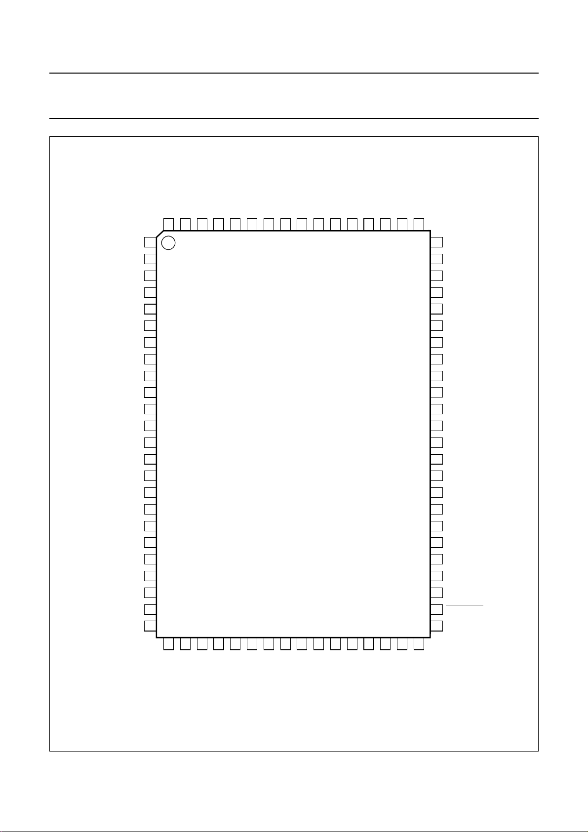
SYMBOL PIN PIN TYPE DESCRIPTION
VDACP 1 AP2D positive reference voltage for SCAD1, SCAD2, SCAD3 and level-ADC
VDACN1 2 AP2D ground reference voltage 1 for SCAD1, SCAD2, SCAD3 and level-ADC
FML 3 AP2D FM level input; via this pin the level of the FM signal is fed to the SAA7705H; the
level information is needed for a correct functioning of the weak signal behaviour
AML 4 AP2D AM level input; via this pin the level of the AM signal is fed to the SAA7705H
POM 5 AP2D power-on mute of the QDAC; timing is determined by an external capacitor
RRV 6 AP2D rear right audio voltage output of the QDAC
RRI 7 AP2D rear right audio current output of the QDAC
RLI 8 AP2D rear left audio current output of the QDAC
RLV 9 AP2D rear left audio voltage output of the QDAC
V
SSA2
V
DDA2
VREFDA 12 AP2D decoupling for voltage reference of the analog part of the QDAC
FRV 13 AP2D front right audio voltage output of the QDAC
FRI 14 AP2D front right audio current output of the QDAC
FLI 15 AP2D front left audio current output of the QDAC
FLV 16 AP2D front left audio voltage output of the QDAC
TP1 17 BT4CR test pin, used in factory test mode, must not be connected
TP2 18 BT4CR test pin, used in factory test mode, must not be connected
TP3 19 BT4CR test pin, used in factory test mode, must not be connected
TP4 20 BT4CR test pin, used in factory test mode, must not be connected
TP5 21 IBUFD test pin, used in factory test mode, must be connected to V
V
DDD5V1
V
SSD5V1
CD2WS 24 IBUFD word select input 2 from a digital audio source (I2S-bus or LSB-justified format)
CD2DATA 25 IBUFD left or right data input 2 from a digital audio source (I2S-bus or LSB-justified format)
CD2CL 26 IBUFD clock input 2 from a digital audio source (I2S-bus or LSB-justified format)
CD1WS 27 IBUFD word select input 1 from a digital audio source (I2S-bus or LSB-justified format)
CD1DATA 28 IBUFD left or right data input 1 from a digital audio source (I2S-bus or LSB-justified format)
CD1CL 29 IBUFD clock input 1 from a digital audio source (I2S-bus or LSB-justified format)
IISCLK 30 BT4CR clock output to extra DSP chip (I2S-bus)
IISIN1 31 IBUFD data input channel 1 (front) from extra DSP chip (I2S-bus)
IISIN2 32 IBUFD data input channel 2 (rear) from extra DSP chip (I2S-bus)
IISWS 33 BD4CR word select input or output for extra DSP chip (I2S-bus)
IISOUT1 34 BD4CR data output to extra DSP chip (I2S-bus)
IISOUT2 35 BD4CR subwoofer output (I2S-bus)
V
DDD5V2
V
SSD5V2
DSPIN1 38 IBUFD digital input 1 of the DSP core (flag F0 of the status register)
DSPIN2 39 IBUFD digital input 2 of the DSP core (flag F1 of the status register)
10 APVSS ground supply for the analog part of the QDAC
11 APVDD positive supply for the analog part of the QDAC
DDD5V
22 VDDE5 positive supply 1 for peripheral cells
23 VSSE5 ground supply 1 for peripheral cells
36 VDDE5 positive supply 2 for peripheral cells
37 VSSE5 ground supply 2 for peripheral cells
1999 Aug 16 7
Page 8
Philips Semiconductors Preliminary specification
Car radio Digital Signal Processor (DSP) SAA7705H
SYMBOL PIN PIN TYPE DESCRIPTION
DSPOUT1 40 B4CR digital output 1 of the DSP core (flag F2 of the status register)
DSPOUT2 41 B4CR digital output 2 of the DSP core (flag F3 of the status register)
DSPRESET 42 IBUFU reset input to the DSP core (active LOW)
RTCB 43 IBUFD asynchronous reset test control block, connect to ground
SHTCB 44 IBUFD shift clock test control block, connect to ground
TSCAN 45 IBUFD scan control (active HIGH), connect to ground
V
DDD5V3
V
SSD5V3
V
DDD3V1
V
SSD3V1
V
SSD3V2
V
DDD3V2
V
DDD3V3
V
SSD3V3
V
SSD3V4
V
DDD3V4
A0 56 IBUFD I2C-bus address selection
SCL 57 SCHMITCD serial clock input (I2C-bus)
SDA 58 BD4SCI4 serial data input/output (I2C-bus)
RDSCLK 59 BD4CR RDS bit clock output or RDS external clock input
RDSDAT 60 BT4CR RDS data output
SELFR 61 IBUFD AD input selection switch; to enable high-ohmic FMMPX input at fast tuner search
V
SS(OSC)
OSCIN 63 AP2D crystal oscillator input: crystal oscillator sense for gain control or forced input in
OSCOUT 64 AP2D crystal oscillator output: drive output to 11.2896 MHz crystal
V
DD(OSC)
AMAFR 66 AP2D AM audio frequency analog input (right channel)
AMAFL 67 AP2D AM audio frequency analog input (left channel)
TAPER 68 AP2D tape analog input (right channel)
TAPEL 69 AP2D tape analog input (left channel)
CDRI 70 AP2D CD analog input (right channel)
CDRB 71 AP2D feedback input of the CD analog input (right channel)
CDLI 72 AP2D CD analog input (left channel)
CDLB 73 AP2D feedback input of the CD analog input (left channel)
V
DDA1
V
SSA1
VDACN2 76 AP2D ground reference voltage 2 for SCAD1, SCAD2, SCAD3 and level-ADC
46 VDDE5 positive supply 3 for peripheral cells
47 VSSE5 ground supply 3 for peripheral cells
48 VDDI3 positive supply 1 for DSP core
49 VSSI3 ground supply 1 for DSP core
50 VSSI3 ground supply 2 for DSP core
51 VDDI3 positive supply 2 for DSP core
52 VDDI3 positive supply 3 for DSP core
53 VSSI3 ground supply 3 for DSP core
54 VSSI3 ground supply 4 for DSP core
55 VDDI3 positive supply 4 for DSP core
on pin FMRDS; if SELFR is HIGH, the input at pin FMRDS is put through to SCAD1
and FMRDS gets high-ohmic; this pin works together with the AD register bit
SELTWOTUN (see Table 9)
62 APVSS ground supply for crystal oscillator circuit
slave mode
65 APVDD positive supply for crystal oscillator circuit
74 APVDD analog positive supply for SCAD1, SCAD2, SCAD3 and level-ADC
75 APVSS analog ground supply SCAD1, SCAD2, SCAD3 and level-ADC
1999 Aug 16 8
Page 9
Philips Semiconductors Preliminary specification
Car radio Digital Signal Processor (DSP) SAA7705H
SYMBOL PIN PIN TYPE DESCRIPTION
CDGND 77 AP2D positive reference for analog CD block
VREFAD 78 AP2D common-mode reference voltage SCAD1, SCAD2, SCAD3 and level-ADC
FMRDS 79 AP2D FM RDS analog input
FMMPX 80 AP2D FM multiplex analog input
Table 1 Explanation of pin types
PIN TYPE DESCRIPTION
AP2D analog input/output
APVDD analog supply
APVSS analog ground
VDDE5 5 V peripheral supply
VSSE5 5 V peripheral ground connection, no connection to the substrate
VDDI3 3.3 V supply to digital core and internal I/O pads
VSSI3 3.3 V ground to digital core and internal I/O pads, no connection to the substrate
SCHMITCD CMOS, Schmitt trigger input with active pull-down
IBUFU CMOS, active pull-up to all VDDE5 pads
IBUFD CMOS, active pull-down to all VSSE5 pads
BD4CR bidirectional CMOS I/O buffer, 4 mA, slew rate control
BT4CR 4 mA CMOS 3-state output buffer, slew rate control
B4CR 4 mA CMOS output buffer, slew rate control
BD4SCI4 CMOS I/O pad with open-drain output
1999 Aug 16 9
Page 10
Philips Semiconductors Preliminary specification
Car radio Digital Signal Processor (DSP) SAA7705H
handbook, full pagewidth
SSA1
VDACP
VDACN1
POM
RRV
V
SSA2
V
DDA2
VREFDA
V
DDD5V1
V
SSD5V1
CD2WS
FML
AML
RRI
RLI
RLV
FRV
FRI
FLI
FLV
TP1
TP2
TP3
TP4
TP5
CDGND
77
VDACN2
76
FMMPX
FMRDS
VREFAD
80
79
78
1
2
3
4
5
6
7
8
9
10
11
12
13
14
15
16
17
18
19
20
21
22
23
24
V
75
DDA1
V
CDLB
74
73
SAA7705H
CDLI
72
CDRB
71
CDRI
70
TAPEL
69
TAPER
68
AMAFL
67
AMAFR
V
66
DD(OSC)
65
64
63
62
61
60
59
58
57
56
55
54
53
52
51
50
49
48
47
46
45
44
43
42
41
OSCOUT
OSCIN
V
SS(OSC)
SELFR
RDSDAT
RDSCLK
SDA
SCL
A0
V
DDD3V4
V
SSD3V4
V
SSD3V3
V
DDD3V3
V
DDD3V2
V
SSD3V2
V
SSD3V1
V
DDD3V1
V
SSD5V3
V
DDD5V3
TSCAN
SHTCB
RTCB
DSPRESET
DSPOUT2
25
26
27
28
29
30
31
32
IISIN1
CD2CL
CD2DATA
CD1WS
CD1DATA
CD1CL
IISCLK
IISIN2
Fig.2 Pin configuration.
1999 Aug 16 10
33
IISWS
34
35
IISOUT1
IISOUT2
36
DDD5V2
V
V
37
38
DSPIN1
SSD5V2
39
40
DSPIN2
DSPOUT1
MGM118
Page 11

Philips Semiconductors Preliminary specification
Car radio Digital Signal Processor (DSP) SAA7705H
8 FUNCTIONAL DESCRIPTION
The SAA7705H consists of a DSP core and periphery.
The DSP core is described in Sections 8.6, 8.7 and 8.11.
The periphery handles the following tasks:
• FM and level information processing (see Section 8.1)
• Analog source selection and analog-to-digital
conversion of the analog audio sources (see
Section 8.2)
• Digital-to-analog conversion of the DSP output QDAC
(see Section 8.3)
• Clock circuit and oscillator (see Section 8.4)
• Equalizer accelerator circuit (see Section 8.5)
• I2C-bus interface (see Section 8.8 and Chapter 12)
• RDS decoder (see Section 8.10).
8.1 FM and level information processing
8.1.1 SIGNAL PATH FOR LEVEL INFORMATION
For FM weak signal processing and for AM and FM
purposes (absolute level and multipath), an FM level and
an AM level input is implemented (pins FML and AML).
In the case ofradio reception clocking of the filters andthe
level-ADC is based on a 38 kHz sample frequency.
The DC input signal is converted by a bitstream first-order
Sigma-Delta ADC followed by a decimation filter.
The input signal has to be obtained from the radio part.
Two different configurations for AM and FM reception are
possible:
• Acircuitwith two separate level signals:oneforFM level
and one for AM level
• A combined circuit with AM and FM level information on
the FM level input.
The level input is selected with bit LEVAM-FM of the SEL
register (see Table 12 and Chapter 12).
8.1.2 SIGNAL PATH FROM FMMPX INPUT TO IAC AND
STEREO DECODER
The SAA7705H has four analog audio source channels.
One of the analog inputs is the FM multiplex signal.
Selection of this signal can be achieved by the SEL
register bits AUX-FM and CD-TAPE (see Table 12).
The multiplexed FM signal is converted to the digital
domain in SCAD1, a bitstream third-order SCAD. The first
decimation with a factor of 16 takes place in down sample
filter ADF1. This decimation filter can be switched by
means of the SEL register bit WIDE-NARROW
(see Table 12)in the wide ornarrowband position. In case
of FM reception, it must be in the narrow position.
The FMMPX path is followed by the sample-and-hold
switch of the IAC (see Section 8.1.5) and the 19 kHz pilot
signal regeneration circuit. A second decimation filter
reduces the output of the IAC to a lower sample rate.
One of the two filter outputs contains the multiplexed
signal with a frequency range of 0 to 60 kHz.
The outputs of this signal path to the DSP (which are all
running on a sample frequency of 38 kHz) are:
• Pilot presence indication: Pilot-I. This one bit signal is
LOW for a pilot frequency deviation <4 kHz and HIGH
for a pilot frequency deviation >4 kHz and locked on a
pilot tone.
• FM reception stereo signal. This is the 18-bit output of
the stereo decoder after the matrix decoding in
Information System Network (ISN) I2S-bus format.
This signal is fed via a multiplexer to a general I2S-bus
interface block that communicates with the DSP core.
• A noise level indication. This signal is derived from the
first MPX decimation filter via a wide band noise filter.
Detection is done with an envelope detector. This noise
level is filtered in the DSP core and is used to optimize
the FM weak signal processing.
8.1.3 INPUT SENSITIVITY FOR FM AND RDS SIGNALS
The FM and RDS input sensitivity is designed for tuner
front ends which deliver an output voltage varying from
65 to 225 mV (RMS) at a sweep of 22.5 kHz for a 1 kHz
tone. The intermediate standard input sensitivities can be
reached in steps of 1.6 dB, to be programmed with the
AD register bits VOLFM and VOLRDS (see Tables 9
and 17). The volume control of the FMMPX and the
FMRDS input can be controlled separately. VOLFM and
VOLRDS = 000is the most sensitive position,VOLFMand
VOLRDS = 111 the least sensitive position. Due to the
analog circuit control of the volume gain, the input
impedanceofpin FMMPX or pin FMRDS changes withthe
volume setting.
8.1.4 AD INPUT SELECTION SWITCH
Pin SELFR makes it possible to change to another
transmitter frequency with the same radio program to
assess the quality of that signal. In case of a stronger
transmitter signal the decision can be made by the
software to switch to the new transmitter. The FMMPX
input is normally used to process the FM signal.
This FMMPX input is connected via a relative large
capacitor to the MPX tuner output. Switching the tuner to
another transmitter frequency means another DC voltage
level on the MPX output of the tuner and a charging of the
1999 Aug 16 11
Page 12
Philips Semiconductors Preliminary specification
Car radio Digital Signal Processor (DSP) SAA7705H
series capacitor (because the FMMPX input of the
SAA7705H is low-ohmic). Pulling SELFR HIGH during
such an update, causes the FMMPX input to become
high-ohmic, preventing charging of the capacitor.
The signal probing of the new transmitter quality is done
via the FMRDS input.
8.1.5 INTERFERENCE ABSORPTION CIRCUIT The Interference Absorption Circuit (IAC) detects and
suppresses ignition interference. This hardware IAC is a
modified, digitized and extended version of the analog
circuit which is in use for many years already.
The IAC consists of an MPX mute function switched by
mutepulses from two ignitioninterferencepulse detectors.
A third detector inhibits muting.
The three detectors are:
• Interference detector: The input signal of the first
detectoris the output signal ofSCAD1.Thisinterference
detector analyses the high frequency contents of the
MPX signal. The discrimination between interference
pulses and other signals is performed by a special
Philips patented fuzzy logic such as algorithm and is
based on probability calculations. This detector
performs optimally with higher antenna voltages.
On detection of ignition interference, this logic will send
appropriate pulses to the MPX mute switch.
• Level detector: The input signal of the second detector
is the FM level signal (the output of the level-ADC).
This detector performs optimally with lower antenna
voltages. It is therefore complementary to the first
detector.Thecharacteristicsofbothignitioninterference
pulse detectors can be adapted to the properties of
different FM front ends by means of the coefficients in
the IAC register and the level-IAC register
(see Section 12.4). Both IAC detectors can be switched
on or off independently. Both IAC detectors can mute
the MPX signal independently.
• Dynamic detector: The third detector is the dynamic
IAC circuit. This detector switches off the IAC
completelyif the frequency deviationof the FM multiplex
signal is too high. The use of narrow band IF filters can
result in AM modulation. This AM modulation could be
interpreted by the IAC circuitry as interference caused
by the car’s engine.
handbook, full pagewidth
FML 3
AML 4
AMAFR 66
TAPER 68
CDRB 71
CDRI 70
CDGND 77
AMAFL 67
TAPEL 69
CDLB 73
CDLI 72
FMMPX 80
FMRDS 79
SELFR 61
SELECTOR
ROUTER
GAIN
CONTROL
Fig.3 Analog input switching circuit.
LEVEL-ADC
SCAD2
INPUT
SCAD1
SCAD3
MGM123
1999 Aug 16 12
Page 13

Philips Semiconductors Preliminary specification
Car radio Digital Signal Processor (DSP) SAA7705H
Parameter setting for the IAC detectors is done by means
of 5 different coefficients. Upon reset, the nominal setting
for a good performing IAC detector is selected.
8.1.5.1 AGC set point (1 bit)
In case the sensitivity and feed-forward factor are out of
range in a certain application, the set point of the AGC
can be shifted. The set point controls the sensitivity of
the other IAC control parameters. See bit 11 of the IAC
register (Table 11).
8.1.5.2 Threshold sensitivity offset (3 bits)
With this parameter the threshold sensitivity of the
comparator in the interfering pulse detectors can be set.
It also influences the amount of unwanted triggering.
Settings are according to Table 25.
8.1.5.3 Deviation feed-forward factor (3 bits)
This parameter determines the reduction of the sensitivity
of the detector by the absolute value of the MPX signal.
This mechanism prevents the detector from unwanted
triggering at noise with modulation peaks. In Table 24 the
possible values are given.
8.1.5.4 Suppression stretch time (3 bits)
This parameter sets the duration of the pulse suppression
after the detector has stopped sending a trigger pulse.
It can be switched off by setting the value ‘000’.
The duration can be selected in steps of one period of the
304 kHz (3.3 µs) sample frequency. In Table 23 the
possible values are given.
8.1.5.5 MPX delay (2 bits)
With this parameter the delay time between
2 and 5 samples of the 304 kHz sample frequency can be
selected. The needed value depends on the used front
end of the car radio. Settings are according to Table 22.
via the FMdemodulator and MPX conversion and filtering.
These differences depend on the front end used in the car
radio. With a simultaneous appearance of a peak
disturbance at the FM level input and the MPX ADC input
of the IC, a zero delay setting takes care for the level-IAC
mutepulse to coincidewiththe passage of thedisturbance
in the MPX mute circuit. The setting for the level-IAC
feed-forward allows to advance the mute pulse by
1 sample period or to delay it by 1 or 2 sample periods of
the 304 kHz clock, with respect to the default value.
The appropriate register bits for each setting are given in
Table 20.
8.1.5.8 Level-IAC suppression stretch time (2 bits)
This parameter sets the time that the mute pulse is
stretched when the FM level input has stopped exceeding
thethreshold. The durationcanbe selected insteps of one
period of the 304 kHz (3.3 µs) sample frequency.
In Table 19 the possible values are given.
8.1.5.9 Dynamic IAC threshold levels
If enabled by bit 15 of the LEVELIAC register, this block
will disable temporarily all IAC actions if the MPX mono
signal exceeds a threshold deviation (threshold 1) for a
given time with a given excess amount (threshold 2). This
MPX mono signal is separated from the MPX signal witha
low-pass filter with the −3 dB corner point at 15 kHz.
The possible values of this threshold are given in
Table 18.
8.1.5.10 IAC testing mode
The internal IAC trigger signal is visible on pin DSPOUT2
if bit IACTRIGGER of the IAC register is set. In this mode
the effect of the parameter settings on the IAC
performance can be verified.
8.2 Analog source selection and analog-to-digital
conversion
8.1.5.6 Level-IAC threshold (4 bits)
With this parameterthe sensitivity of the comparator in the
ignition interference pulse detector can be set. It also
influences the amount of unwanted triggering.
The possible values are given in Table 21. The prefix
value ‘0000’ switches off the level-IAC function.
8.1.5.7 Level-IAC feed-forward setting (2 bits)
This parameter allows for adjusting delay differences in
the signal paths from the FM antenna to the MPX mute,
namely, via the FM level-ADC andlevel-IAC detection and
1999 Aug 16 13
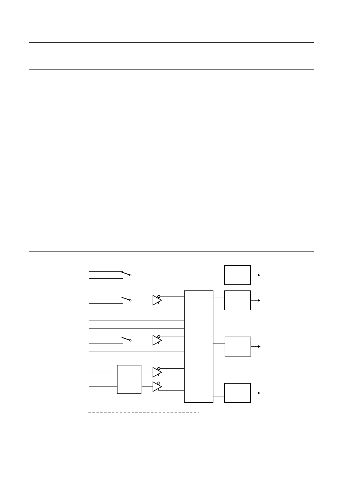
8.2.1 INPUT SELECTION SWITCHES
In Fig.3 the block diagram of the input is shown. The input
selection is controlled by bits in the input selector control
register and the input selection pin SELFR.
The relationship between these bits and the switches is
indicated in Table 26.
8.2.2 SIGNAL FLOW OF THE AM, ANALOG CD AND TAPE
INPUTS
The signal of the two single-ended stereo AM inputs can
be selected by the correct values of the SEL register bits
according to Table 26.
Page 14

Philips Semiconductors Preliminary specification
Car radio Digital Signal Processor (DSP) SAA7705H
The AM and the TAPE inputs are buffered with an
operational amplifier to ensure a high-impedance input
which enables the use of an external resistor divider for
signal reduction. Forcorrect biasing of the first operational
amplifier a resistor must be connected between the input
and pin VREFAD, which acts as a virtual ground (see
Fig.21). The analog input switching circuit is shown in
Fig.3. The input for an analog CD player is explained in
more detail in Section 8.2.3.
8.2.3 THE ANALOG CD BLOCK Special precautions are taken to realize a high
Common-ModeRejectionRatio(CMRR) in case of theuse
of a CD player output processed via analog inputs.
The block diagram is shown in Fig.4. The operational
amplifiers OAR and OAL are used as buffers. The gain of
these operational amplifiers can be adjusted via the
externalresistors and is in thiscase 0.54by using a 8.2 kΩ
and a 15 kΩ resistor.
The reference inputs of these operational amplifiers are
connected to a separate pin CDGND. This pin is on one
side AC connected to the ground shielding of the cable
coming from the CD player and via a resistor >1 MΩ to
pin VREFAD. In this configuration the common-mode
signal propagates all the way to the SCAD block inputs of
SCAD1and SCAD2. TheSCADs themselves havea good
rejection ratio for in-phase common-mode signals.
Which part of the common-mode signal is processed as
the real input signal depends on the ratio of the
CDGND resistor and the series resistor in the cable and
the difference in input offset of the operational amplifiers.
The induced signals onthe CDLI andCDRI lines areof the
same amplitude and therefore rejected as common-mode
signals in the SCADs.
8.2.4 PIN VREFAD
The middle reference voltage of the SCAD1, SCAD2,
SCAD3 and level-ADC can be filtered via this pin.
This voltage is used as half the supply reference of the
SCAD1, SCAD2, SCAD3 and as the positive reference for
thelevel-ADC and buffers.Externalcapacitors (connected
to V
) prevent crosstalk between the SCADs and
SSA1
buffers and improve the power supply rejection ratio of all
blocks. This pin must also be used as a reference for the
inputs AMAFL, AMAFR, TAPEL, TAPER and CDGND.
8.2.5 PINS VDACN1, VDACN2 AND VDACP
These pins are used as ground and positive supply
reference for the SCAD1, SCAD2, SCAD3 and the
level-ADC. For optimal performance, pins VDACN1
and VDACN2 must bedirectly connected tothe V
pin VDACP to the filtered V
DDA1
.
SSA1
and
handbook, full pagewidth
CD-player
analog
output
LEFT
GROUND
RIGHT
15 kΩ
15 kΩ
8.2 kΩ
1 MΩ
8.2 kΩ
off-chip on-chip
Fig.4 Analog CD block.
1999 Aug 16 14
73CDLB
72CDLI
to SCAD2 via router
77CDGND
78VREFAD
71CDRB
70CDRI
OAL
to SCADs and level-ADC
to SCAD1 via router
OAR
MGM124
Page 15
Philips Semiconductors Preliminary specification
Car radio Digital Signal Processor (DSP) SAA7705H
8.2.6 SUPPLY OF THE ANALOG INPUTS The analog input circuit has separate power supply
connections to allow maximum filtering of the analog
supply voltages: V
for the analog ground and V
SSA1
DDA1
for the analog supply.
8.3 Analog outputs
8.3.1 DACS Each of the four low noise high dynamic range DACs
consists of a 15-bit signed magnitude DAC with current
output, followed by a buffer operationalamplifier. For each
of the four audio output channels a separate convertor is
used. Each converter output is connected to the inverting
input of one of the four internal CMOS operational
amplifiers. The non-inverting input of this operational
amplifier is connected to the internal reference voltage.
Together with an internal resistor the conversion of
current-to-voltage of the audio output is achieved.
8.3.2 UPSAMPLE FILTER To reduce spectral components above the audio band, a
fixed 4 times oversampling and interpolating 18-bit digital
IIR filter is used. It is realized as a bit serial design and
consists of two consecutive filters. The data path in these
filters is 22 bits to prevent overflow and to maintain a
signal-to-noiseratio larger then 105 dB. Thewordclock for
theupsample filter (4 × fs)is derived fromthe audio source
timing. If the internal audio source is selected, the sample
frequencycan be either 44.1 or 38 kHz. Incaseofexternal
digital sources (CD1 and CD2), a sample frequency from
32 to 48 kHz is possible.
8.3.3 VOLUME CONTROL
Thetotalvolume control has adynamicrangeof more than
100 dB (0 dB being maximal input on the I2S-bus input).
With the signed magnitude noise shaped 15-bit DAC and
the internal 18-bit registers (these registers provide the
digital data communication between the DSP and the
QDAC) of the DSP core a useful digital volume control
range of 100 dB is possible by calculating the
corresponding coefficients.
The step size is freely programmable and an additional
analog volume control is not needed in this design.
The SNR of the audio output at full-scale is determined by
the total 15 bits of the converter. The noise at low outputs
is fully determined by the noise performance of the DAC.
Since it is a signed magnitude type, the noise at digital
silence is also low. The disadvantage is that the total THD
is higher than conventional DACs. The typical
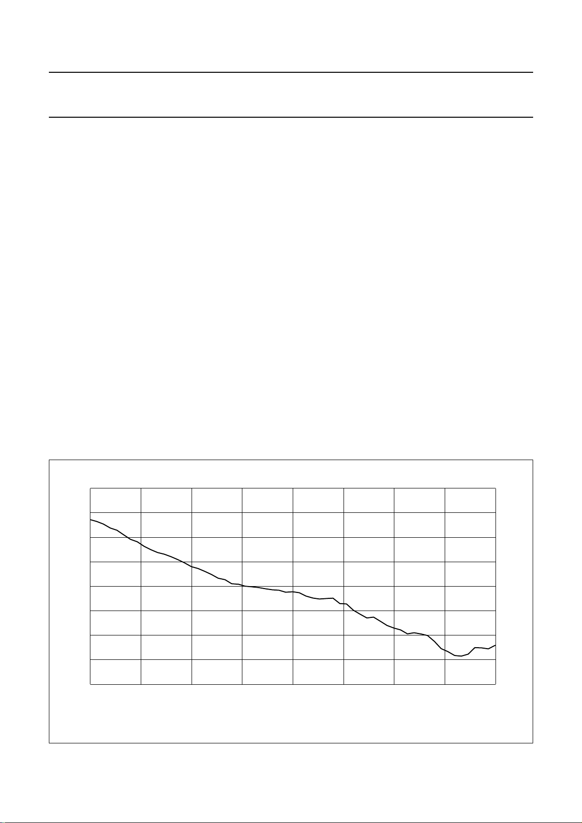
THD-plus-noise versus output level is shown in Fig.5.
handbook, full pagewidth
0
THD + N
(dB)
−20
−30
−40
−50
−60
−70
−80
−90
−80 −70
−40 0−30 −20 −10−60 −50
Fig.5 Typical THD + N curve versus output level.
1999 Aug 16 15
MGM125
output level (dB)
Page 16

Philips Semiconductors Preliminary specification
Car radio Digital Signal Processor (DSP) SAA7705H
8.3.4 FUNCTION OF PIN POM
With pin POM it is possible to switch-off the reference
current of the DAC. The capacitor on pin POM
(see Fig.21) determines the time after which this current
has a soft switch-on. At power-on, the current audiosignal
outputs are always muted. The external capacitor is
loaded in two stages via two different current sources.
The loading starts at a current level that is 9 times lower
than the load current after the voltage on pin POM has
risen above 1 V. This results in an almost dB-linear
behaviour.However, the DAC hasanasymmetrical supply
and the DC output voltage will be half the supply voltage
under functional conditions. During start-up the output
voltage is not defined as long as the supply voltage is
below the threshold voltages of the transistors. A small
jump in DC is possible at start up. In this DC jump audio
components can be present.
8.3.5 POWER-OFF PLOP SUPPRESSION To avoid plops in a power amplifier, the supply voltage
(3.3 V)for the analog partof the DAC canbesupplied from
the 5 V supply via a transistor. A capacitor is connected to
V
to maintain power to the analog part if the 5 V
DDA2
supply is switched off fast. In this case the output voltage
will decrease gradually allowing the power amplifier some
extra time to switch-off without audible plops.
8.3.6 THE INTERNAL PIN VREFDA
8.3.8 SUPPLY OF THE ANALOG OUTPUTS
All the analog circuitry of the DACs and the operational
amplifiers are powered by 2 pins: V
DDA2
and V
SSA2.VDDA2
must have sufficient decoupling to prevent high THD and
to ensure a good Power Supply Rejection Ratio (PSRR).
The digital part of the DAC is fully supplied from the
DSP core supply.
8.4 Clock circuit and oscillator
The device has an on-chip oscillator.The block diagramof
this Pierce oscillator is shown in Fig.6. The active element
neededtocompensateforthe loss resistance of the crystal
is the block Gm. This block is placed between the external
pins OSCIN and OSCOUT. The gain of the oscillator is
internally controlled by the AGC block. A sine wave with a
peak-to-peak voltage close to the oscillator power supply
voltage is generated. The AGC block prevents clipping of
the sine wave and therefore the generation of harmonics
as much as possible. At the same time the voltage of the
sine wave is as high as possible which reduces the jitter
going from the sine wave to the clock signal.
8.4.1 SUPPLY OF THE CRYSTAL OSCILLATOR
The supply of the oscillator is separated from the other
supplies. This minimizes the feedback from the ground
bounce of the chip to the oscillator circuit. Pin V
used as ground and pin V
DD(OSC)
as positive supply.
SS(OSC)
is
Using two internal resistors, half of the supply voltage
V
is obtained and coupled to an internal buffer.
DDA2
This reference voltage is used as a DC voltage for the
output operational amplifiers and as a reference for the
DAC. In order to obtain the lowest noise and to have the
best ripple rejection, a capacitor has to be connected
between this pin and ground.
8.3.7 INTERNAL DAC CURRENT REFERENCE Asa reference for theinternal DAC current andalsofor the
DAC current source output, a current is drawn from
pin VREFDA to V
(ground) via an internal resistor.
SSA2
The value of this resistor determines also the DAC current
(absolute value). Consequently, the absolute value of the
current varies from device to device due to the spread of
the reference resistor value. This, however, has no
influence on the absolute output voltages because these
voltages are derivedfrom a conversion of the DAC current
to the actual output voltage via internal resistors.
1999 Aug 16 16
8.4.2 THE PHASE-LOCKED LOOP CIRCUIT TO GENERATE
THE DSP CLOCK AND OTHER DERIVED CLOCKS
A PLL circuit is used to generate the DSP clock and other
derived clocks.
The minimum equalizer clock frequency is 480fs.
If fsequals 44.1 kHz, this results in a minimum oscillator
frequency of 21.1687 MHz. Crystals for the crystal
oscillator in the range of twice the required DSP clock
frequency (approximately 40 MHz) are always
third-overtone crystals and must be manufactured on
customer demand. This makes these crystals expensive.
The PLL enables the use of a commonly available crystal
operating in fundamental mode. For this circuit a
11.2896 MHz(256 × 44.1 kHz)crystalischosen.Thistype
of crystal is widely used.
Page 17
Philips Semiconductors Preliminary specification
Car radio Digital Signal Processor (DSP) SAA7705H
handbook, full pagewidth
AGC
on-chip
off-chip
G
m
R
bias
63 64
OSCIN OSCOUT
Cx1
Fig.6 Block diagram of the oscillator circuit.
Although multiples of the crystal frequency of
11.2896 MHzfallwithin the FM reception band,thiswillnot
disturb the reception. The relatively low frequency crystal
is driven in a controlled way and the resonating crystal
produces harmonics of a very low amplitude in the FM
reception band.
The block diagram of the programmable PLL is shown in
Fig.7. The oscillator is used in a fundamental mode.
The 11.2896 MHz oscillator frequency is divided by 256
and the resulting signal is fed to the phase detector as a
reference signal. The base for the clock signal is a current
controlled oscillator (free running frequency
70 to 130 MHz).
After having been divided by 4, the required clock
frequency for the DSP core is available. To close the loop
this signal is further divided by 4 and by the PLL clock
division factor N. N can be programmedwith the DCSCTR
register bits PLL-DIV (see Tables 7 and 15) in the range
from 93 to 181. This provides some flexibility in the choice
of the crystal frequency.
With the recommended crystal, N = 154 and the DSP
clockfrequency(f
)equals27.1656 MHz. N = 154 is the
DSP
default position at start-up. By setting the AD register bit
DSPTURBO (see Tables 9 and 15), the PLL output
frequency, and consequently f
, can be doubled.
DSP
This feature is not used in the proposed application.
clock to circuit
65 62
V
DD(OSC)VSS(OSC)
Cx2
MGM126
The clock frequency of the PLL oscillator divided by two
(2f
) is also used as the clock for the DCS block.
DSP
8.4.3 THE CLOCK BLOCK
For the digital stereo decoder a clock signal is needed
which is the 512-multiple of the pilot tone frequency of the
FMmultiplexsignal.This is done by the Digitally Controlled
Sampling (DCS) block, which generates this
512 × 19 kHz = 9.728 MHz clock, the DCS clock, by
locking to the pilot frequency. This block is also able to
generate other frequencies. It is controlled by the
DCSCTR and DCSDIV registers (see Tables 7 and 8).
Default settings of the DCS andthe PLL guaranteecorrect
functioning of the DCS block.
8.4.4 SYNCHRONIZATION WITH THE CORE
In case of I2S-bus input the system can run on audio
sample frequencies of fs= 32 kHz, 38 kHz, 44.1 kHz
or 48 kHz. After processing of an input sample, the Input
flag (I-flag) of the status register (see Section 8.7) of the
DSP core is set to logic 1 during 4 clock cycles on the
falling edge of the internal or external I2S-bus WS pulses.
This flag can be tested with a conditional branch
instruction in the DSP. This synchronisation starts in
parallelwith the input signal duetothe short period thatthe
I-flag is set. It is obvious that the higher fs the lower the
number of cycles available in the DSP program.
1999 Aug 16 17
Page 18
Philips Semiconductors Preliminary specification
Car radio Digital Signal Processor (DSP) SAA7705H
I
handbook, full pagewidth
OSCIN
OSCOUT
V
DD(OSC)
V
SS(OSC)
OSCILLATOR
11.2896 MHz
from
DCSCTR
register
ref
44.1 kHz
÷256
PLL-DIV(0)
PLL-DIV(1)
PLL-DIV(2)
PLL-DIV(3)
×
PHASE
DETECTOR
÷N
Fig.7 Programmable PLL for DSP clock generation.
8.5 Equalizer accelerator circuit
8.5.1 INTRODUCTION The Equalizer accelerator (EQ) circuit is an equalizer
circuit used as a hardware accelerator to the DSP core.
Its inputs and outputs are stored in registers of the
DSP core (these registers provide the digital data
communication between the equalizer and the DSP core).
The flag that starts the DSP program, refreshes the EQ
input and output registers and starts the EQ controller.
The EQ circuit contains one second-order filter data path
that is twenty-fold multiplexed. With this circuit, a
two-channel equalizer of 10 second-order sections per
channel or a four-channel equalizer of 5 second-order
sections per channel can be realized.
The centre frequency, gain and Q-factor of all
20 second-order sections can be set independently from
each other. Every section is followed by a variable
attenuation of 0 or 6 dB. Per section, 4 bytes are needed
to store the settings. During an audio sample period, all
settings are read as 16-bit words in 80 read accesses to
the coefficient memory.
I
delay
70 to
130 MHz
LOOP
FILTER
N = 154
CURRENT CONTROLLED OSCILLATOR
÷2 ÷2÷2÷2
clock clock
27.1656 MHz 54.3312 MHz
MGM127
8.5.2 EQ CIRCUIT OVERVIEW
This EQ circuit contains the following parts:
• A second-order filter data path, with programmable
coefficients and with 40 state registers, supporting
storage of the two filter states for 20 multiplexed filters;
this part is clocked by a gated clock
• Signal routing around this filter data path, consisting of:
– busesand selectors to configurethe 20 filter sections
for two or four channels;
– inputandoutputregisters,withproperinterfacingwith
the DSP core and with conversions between parallel
and serial formats.
• A coefficient memory, to be loaded via the I2C-bus
interface
• A controller, started by the write pulse for input and
outputregisters, that controls thesignalrouting, controls
the clock for the filter data path, addresses the
coefficient memory and controls its programming.
1999 Aug 16 18
Page 19

Philips Semiconductors Preliminary specification
Car radio Digital Signal Processor (DSP) SAA7705H
Table 2 Equalizer port list
NAME DESCRIPTION
Data to/from DSP core
IN FL Front Left input bus, 18 bits
IN FR Front Right input bus, 18 bits
IN RL Rear Left input bus, 18 bits
IN RR Rear Right input bus, 18 bits
OUT FL Front Left output bus, 18 bits
OUT FR Front Right output bus, 18 bits
OUT RL Rear Left output bus, 18 bits
OUT RR Rear Right output bus, 18 bits
From EQ register
TWO-FOUR two or four channel configuration
switch, I2C-bus controlled; see Table 9
Control from DSP
clk
CORE
DSP core clock, at least 480f
s
start new sample start pulse, input and
output registers written
data-valid new coefficient word available
acknowledge new coefficient word loaded in
coefficient memory
new-address address for newcoefficient word, 6 bits,
range is from 0 to 39
new-coefword new coefficient word, 16 bits
In Table 2 the port pinning is depicted. This equalizer
accelerator circuit (EQ)can make a two-channel equalizer
of 10 second-order sectionsper channel or a four-channel
equalizer of 5 second-order sections per channel
depending on the value of AD register bit TWO-FOUR
(see Table 9). It takes an input sample set of 2 (stereo)
samples or 4 (stereo front and rear) samples via 4 input
registers. It delivers an output sample set of 2 or
4 samples via 4 output registers. All input and output
registers are 18 bits wide.
A pulse of three clock cycles long of the signal start based
on the word select of the used signal path refreshes the
EQ input and output registers and starts up the EQ
controller.
This sequence is shown in Fig.8.
8.5.3 CONTROLLER AND PROGRAMMING CIRCUIT A controller is used to generate the bit control and
word control signals for the filter section data path, the
addresses for the coefficient memory and the control
signals for the input and output selections and
conversions. Depending on the AD register
bit TWO-FOUR (see Table 9), control signals for a two- or
four-channel equalizer are generated.
The 40 coefficient words should be addressed via
40 registers (addresses 0F80H to 0FA7H).
The new coefficient word rate must be slower than 0.5fs,
e.g. 22 kHz. The equalizer is programmed by dedicated
software.
handbook, full pagewidth
clk
CORE
start
480 clk
gated clock
CORE
cycles
Fig.8 Derivation of the gated clock from clk
1999 Aug 16 19
audio sample period
CORE
MGM128
.
Page 20

Philips Semiconductors Preliminary specification
Car radio Digital Signal Processor (DSP) SAA7705H
8.6 The DSP core
This IC comprises a DSP core (the actual programmable
embedded calculating machine) that is adapted to the
required calculation power needed and as such is
optimized on area.
This DSP core is also known under the name EPICS6, of
which EPICS is the generic name of this type of DSP and
6 is the version number. This DSP is mainly a calculator
designed for real time processing (at fs= 38 or 44.1 kHz)
of the digitized audio data stream. A DSP is especially
suited to calculate the sum of products of the data words
representingthe audio data. SeeChapter 13for document
references on EPICS6.
8.7 External control pins and status register
The DSP core contains a 9-bit status register.
These 9 flags contain information which is used by the
conditionalbranch logic ofthe DSP core. Forexternal use,
the flags F0, F1, F2 and F3 are available. Pins DSPIN1
and DSPIN2 control the status of the flags F0 and F1.
The two status flags F3 and F4 are controlled by the
DSP core and can be read via the pins DSPOUT1
and DSPOUT2. The function of each pin depends on the
DSPprogram. Another importantflagis the I-flag.Thisflag
is an input flag and is set the moment new I2S-bus data or
another type of digital audio data is available to the
DSP core.
2
8.8 I
The I2C-bus format is described in
to use it”
C-bus interface (pins SCL and SDA)
“The I2C-bus and how
, order no. 9398 393 40011.
For the external control of the SAA7705H a fast I2C-bus is
implemented. This is a 400 kHz bus which is downward
compatible with the standard 100 kHz bus.
There are three different types of control instructions:
• Instructions to control the DSP program, programming
the coefficient RAM and reading the values of
parameters (level, multipath etc.)
• Instructions to control the equalizer and to program the
equalizer coefficient RAM to be able to change the
centre frequency, gain and Q-factor of the equalizer
sections
• Instructions controlling the I
2
S-bus data flow, such as
source selection, IAC control and clock speed.
The detailed descriptionof the I2C-bus and thedescription
of the different bits in the memory map is given in
Chapter 12.
8.9 I
2
S-bus inputs and outputs
For communication with external digital sources, the
I2S-busdigitalinterface bus is used. Itisaserial3-line bus,
having one line for data, one line for clock and one line for
the word select. For external digital sources the
SAA7705H acts as a slave, so the external source is
master and supplies the clock.
The I2S-bus input is capable of handling Philips I2S-bus
and LSB-justified formats of 16, 18 and 20-bit word sizes.
The selection of the digital audio format is described in
Tables 13 and 28. See Fig.9 for the general waveform
formats of the four possible formats.
The number of bit clock (BCK) pulses may vary in the
application. When the applied word length is shorter than
18 bits (internal resolution), the LSBs will get internally a
random value. When the applied word length exceeds
18 bits, the LSBs are skipped.
Theinput circuitry islimited in handlingthe number ofBCK
pulses per WS period. The maximum allowed number of
bit clocks per WS channel (half of the symmetrical WS
period) is 128.
The DSP program is synchronized with the external
source via the word select signal. On every negative edge
of the IISWS the I-flag of the status register is set.
1999 Aug 16 20
Page 21

This text is here in white to force landscape pages to be rotated correctly when browsing through the pdf in the Acrobat reader.This text is here in
ha
_white to force landscape pages to be rotated correctly when browsing through the pdf in the Acrobat reader.This text is here inThis text is here in
white to force landscape pages to be rotated correctly when browsing through the pdf in the Acrobat reader. white to force landscape pages to be ...
1999 Aug 16 21
ndbook, full pagewidth
Philips Semiconductors Preliminary specification
Car radio Digital Signal Processor (DSP) SAA7705H
WS
BCK
DATA
WS
BCK
DATA
WS
BCK
DATA
WS
BCK
MSB B2
LEFT
MSB MSBB2
INPUT FORMAT I
LEFT
LEFT
MSB B2 B3 B4
LEFT
21> = 812 3
2
S-BUS
RIGHT
3
16
15 2 1
MSB
B2
16
1518 17 2 1
16
1518 1720 19 2 1
> = 8
B15
LSB
LSB JUSTIFIED FORMAT 16 BITS
B17
LSB
LSB JUSTIFIED FORMAT 18 BITS
RIGHT
RIGHT
RIGHT
16
MSB B2
16 1518 17 2 1
MSB B2 B3 B4
16
15 2 1
B15 LSB
B17 LSB
1518 1720 19 2 1
DATA
MSB B2 B3 B4 B5 B6
Fig.9 Available serial digital audio data in/output formats.
B19
LSB
LSB JUSTIFIED FORMAT 20 BITS
MSB B2 B3 B4 B5 B6
B19 LSB
MGL808
Page 22

Philips Semiconductors Preliminary specification
Car radio Digital Signal Processor (DSP) SAA7705H
8.10 RDS decoder (pins RDSCLK and RDSDAT)
The RDS decoder recovers the additional inaudible RDS
informationwhich is transmitted byFMradio broadcasting.
The (buffered) data is provided as output for further
processing by a suitable decoder. The operational
functions of the decoder are in accordance with the
“European Broadcasting Union (EBU) specification
EN 50067”
.
The RDS decoder has three different functions:
• Clock and data recovery from the FM multiplex signal
• Buffering of 16 bits, if selected
• Interfacing with the microcontroller.
8.10.1 CLOCK AND DATA RECOVERY The RDS chain has a separate input. This enables RDS
updates during tape play and also the use of a second
receiverformonitoringthe RDS information of signals from
another transmitter (double tuner concept). It can as such
be done without interruption of the audio program.
The MPX signal from the main tuner of the car radio can
be connected to this RDS input via the built-in source
selector. The input selection is controlled by
bit RDS-CLKIN of the RDSCTR register (see Table 14).
The RDS chain contains a third-order Sigma-Delta ADC,
followedbytwo decimation filters. The firstfilterpassesthe
multiplex band including the signals around 57 kHz and
reduces the Sigma-Delta noise.
The second filter reduces the RDS bandwidth around
57 kHz.
The quadrature mixer converts the RDS band to the
frequency spectrum around 0 Hz and contains the
appropriate Q/I signal filters. The final decoder with
CORDIC recovers the clock and data signals.
These signals are output on pins RDSCLK and RDSDAT.
8.10.2 TIMING OF CLOCK AND DATA SIGNALS
The timing of the clock and data output is derived from the
incoming data signal. Under stable conditions the data will
remain valid for 400 µs after the clock transition.
The timing of the data change is 100 µs before a positive
clock change. This timing is suited for positive as well as
negative triggered interrupts on a microcontroller.
The RDS timing is shown in Fig.10.
During poor reception it is possible that faults in phase
occur, then theduty cycle of the clock and datasignals will
vary from minimum 0.5 times to a maximum of 1.5 times
the standard clock periods. Normally, faults in phase do
not occur on a cyclic basis.
8.10.3 BUFFERING OF RDS DATA
The repetition of the RDS data is around the 1187 Hz.
This results in an interrupt on the microcontroller for every
842 µs.In a secondmode, the RDSinterface has a double
16-bit buffer.
handbook, full pagewidth
RDSDAT
RDSCLK
t
s
T
cy
Fig.10 RDS timing (direct output mode).
1999 Aug 16 22
t
HC
t
LC
t
d
MBH175
Page 23

Philips Semiconductors Preliminary specification
Car radio Digital Signal Processor (DSP) SAA7705H
handbook, full pagewidth
RDSDAT
RDSCLK
t
w
block ready start reading data
D0 D1 D2 D13 D14 D15
t
T
cy
HC
Fig.11 Interface signals RDS decoder and microcontroller (buffer mode).
8.10.4 BUFFER INTERFACE The RDS interface buffers 16 data bits. Every time 16 bits
are received, the data line is pulled LOW and the buffer is
overwritten. The microcontroller has to monitor the data
line in at most every 13.5 ms. This mode is selected by
setting the RDS-CLKIN bit of the RDSCTR register
(see Table 14) to logic 1. In Fig.11 the interface signals
from the RDS decoder and the microcontroller in buffer
mode are shown. When the buffer is filled with 16 bits the
data line is pulled LOW. The data line will remain LOW
until reading ofthe buffer isstarted by pulling the clockline
LOW. The first bit is clocked out. After 16 clock pulses the
reading of the buffer is ready and the data line is set HIGH
until the buffer is filled again. The microcontroller stops
communication by pulling the line HIGH. The data is
written out just after the clock HIGH-to-LOW transition.
The data is valid when the clock is HIGH.
When a new 16 bits buffer is filled before the other buffer
is read, that buffer will be overwritten and the old data is
lost.
t
LC
MBH176
A more or less fixed relationshipbetween the DSPRESET
and the POM time constant isrequired. The voltageon the
pin POM determines the current flowing in the DACs.
When pin POM is at 0 V the DAC currents and output
voltages are zero; at V
voltage the DAC currents are
DDA2
at their nominal (maximum) value. Some time before the
QDAC outputs get to their nominal output voltages, the
DSP must be in working mode to reset the output register.
Therefore the DSP time constant must be less than the
POM time constant. For recommended capacitors,
see Figs 21 and 22.
The reset has the following functions:
• The bits of the IAC control register are set to logic 0
• The bits of the SEL register are set to their nominal
values
• The DSP status registers are reset
• The program counter is set to address 0000H
• The two output flags in the status register are reset to
logic 0 (pins DSPOUT1 and DSPOUT2 are LOW).
8.11 DSP reset
Pin DSPRESET is active LOW and hasan internal pull-up
resistor. Between this pin and pin V
SSD3V
a capacitor
should be connected to allow a proper switch-on of the
supply voltage. The capacitor value is suchthat thechip is
in reset state as long as the power supply is not stabilized.
1999 Aug 16 23
When the level on pin DSPRESET is HIGH, the DSP
program starts to run.
Page 24

Philips Semiconductors Preliminary specification
Car radio Digital Signal Processor (DSP) SAA7705H
9 LIMITING VALUES
In accordance with the Absolute Maximum Rating System (IEC 134).
SYMBOL PARAMETER CONDITIONS MIN. MAX. UNIT
V
DDD3V
V
DDD5V
∆V
DDD3Vx
∆V
DDD5Vx
I
IK
I
OK
I
O(sink/source)
I
DD
I
SS
T
amb
T
stg
V
ESD
I
lu(prot)
P/out power dissipation per output − 100 mW
P
tot
supply voltage −0.5 +5 V
supply voltage only valid for the voltages in
−0.5 +6.5 V
connection with the 5 V I/Os
voltage difference between any
two V
DDD3Vx
pins
voltage difference between any
two V
DDD5Vx
pins
− 550 mV
− 550 mV
DC input clamping diode current VI< −0.5 V or VI>VDD+ 0.5 V −±10 mA
DC output clamping diode
current
output type 4 mA (BD4CR,
BT4CR and B4CR); VO< −0.5 V
−±20 mA
or VO>VDD+ 0.5 V
DC output sink or source current output type 4 mA (BD4CR,
−±20 mA
BT4CR and B4CR);
−0.5<VO<VDD+ 0.5 V
DC supply current per pin −±750 mA
DC ground supply current per pin −±750 mA
ambient temperature −40 +85 °C
storage temperature −65 +150 °C
ESD voltage
human body model 100 pF; 1500 Ω 3000 − V
machine model 100 pF; 2.5 µH; 0 Ω 300 − V
latch-up protection current CIC specification/test method 100 − mA
total power dissipation − 1600 mW
10 THERMAL CHARACTERISTICS
SYMBOL PARAMETER CONDITION VALUE UNIT
R
th(j-a)
thermal resistance from junction to ambient mounted on printed-circuit board 45 K/W
1999 Aug 16 24
Page 25

Philips Semiconductors Preliminary specification
Car radio Digital Signal Processor (DSP) SAA7705H
11 CHARACTERISTICS
SYMBOL PARAMETER CONDITIONS MIN. TYP. MAX. UNIT
Supplies; T
V
DDD3V
V
DDA
V
DDA1
V
DDD5V
I
DDD3V
I
DDD5V
I
DDA1
I
DDA2
I
DD(OSC)
P
tot
Digital I/O; T
V
IH
V
IL
V
hys
V
OH
V
OL
= −40 to +85 °C; V
amb
digital supply voltage
3.3 V for DSP core
analog supply voltage
3.3 V
= 4.5 to 5.5 V; V
DDD5V
V
DDD3Vx
to V
V
DDAx
V
SS
pins with respect
SS
pins with respect to
supply voltage analog
part ADC
supply voltage 5 V for
periphery
supply current of the
3.3 V digital DSP core
V
DDD5Vx
to V
pins with respect
SS
high activity of the DSP at
27 MHz DSP frequency
supply current of the
5 V digital periphery
supply current of the
ADCs
zero input and output
signal
supply current of the
DACs
supply current crystal
oscillator
at start-up − 715mA
at oscillation − 0.6 2 mA
total power dissipation high activity of the DSP at
27 MHz DSP frequency
= −40 to +85 °C; V
amb
= 4.5 to 5.5 V; V
DDD5V
HIGH-level input
voltageall digital inputs
and I/Os; pin types:
IBUFD, IBUFU,
BD4CR, SCHMITCD
LOW-level input
voltageall digital inputs
and I/Os; pin types:
IBUFD, IBUFU,
BD4CR, SCHMITCD
hysteresis voltage; pin
type: SCHMITCD
HIGH-level output
IO= −4mA V
voltage digital outputs;
pin types: B4CR,
BD4CR
LOW-level output
V
DDD5V
= 4.5 V; IO=4mA −−0.4 V
voltage digital outputs;
pin types: B4CR,
BD4CR
DDD3V
DDD3V
= 3 to 3.6 V
3 3.3 3.6 V
3 3.3 3.6 V
3 3.3 3.6 V
4.5 5 5.5 V
− 80 110 mA
− 35 mA
− 35 43 mA
− 45 mA
− 0.352 0.535 W
= 3 to 3.6 V
0.7V
DDD5V
−−0.3V
−− V
DDD5V
V
1 1.3 − V
− 0.4 −− V
DDD5V
1999 Aug 16 25
Page 26

Philips Semiconductors Preliminary specification
Car radio Digital Signal Processor (DSP) SAA7705H
SYMBOL PARAMETER CONDITIONS MIN. TYP. MAX. UNIT
V
OL(SDA)
I
LO
R
pu(VDDD)(int)
R
pd(VSSD)(int)
t
i(r)
t
i(f)
t
o(r)(min)
t
o(r)(max)
t
o(f)(min)
LOW-level output
voltage I2C-bus data
output (SDA); pin type:
BD8SCI4
output leakage current
3-state outputs; pin
types: BD4CR,
BD8SCI4
internal pull-up resistor
to V
DDD5V
; pin type:
IBUFU
internal pull-down
resistor to V
SSD5V
; pin
type: IBUFD
input rise time V
input fall time V
minimum output rise
time
digitaloutputsexcept
I2C-bus data output;
pin types:
B(D)(T)4CR
I2C-bus data output;
pin type: BD4SCI4
maximum output rise
time
digitaloutputsexcept
I2C-bus data output;
pin types:
B(D)(T)4CR
I2C-bus data output;
pin type: BD4SCI4
minimum output fall
time
digitaloutputsexcept
I2C-bus data output;
pin types:
B(D)(T)4CR
I2C-bus data output;
pin type: BD4SCI4
IO=8mA −−0.4 V
VO= 0 V or V
DD5V
−−±5 µA
23 50 80 kΩ
23 50 80 kΩ
= 5.5 V − 6 200 ns
DDD5V
= 5.5 V − 6 200 ns
DDD5V
V
V
DDD5V
DDD3V
= 5.5 V;
= 3.6 V;
Tj= −40 °C
CL= 30 pF 7.6 − 18.4 ns
CL= 200 pF tbf tbf tbf ns
V
V
= 4.5 V;
DDD5V
=3V; Tj= 125 °C
DDD3V
CL= 30 pF 13.7 − 33.4 ns
CL= 200 pF tbf tbf tbf tbf
V
V
DDD5V
DDD3V
= 5.5 V;
= 3.6 V;
Tj= −40 °C
CL=30pF 7 − 17 ns
CL= 200 pF tbf tbf tbf ns
1999 Aug 16 26
Page 27

Philips Semiconductors Preliminary specification
Car radio Digital Signal Processor (DSP) SAA7705H
SYMBOL PARAMETER CONDITIONS MIN. TYP. MAX. UNIT
t
o(f)(max)
DC characteristics analog inputs; T
V
REFAD
Z
o(VREFAD)
V
VDACP
I
VDACP
V
V
I
VDACN1
I
VDACN2
V
VDACN1
VDACN2
IO(SCAD)
,
,
AC characteristics analog inputs; T
V
i(con)(max)(rms)
R
i
R
i(FMMPX)
THD
FMMPX
S/N
FMMPX(m)
maximum output fall
time
digitaloutputsexcept
I2C-bus data output;
pin types:
B(D)(T)4CR
I2C-bus data output;
pin type: BD4SCI4
common-mode
reference voltage for
SCAD1, 2, 3 and
level-ADC
output impedance at
pin VREFAD
positive reference
voltage SCAD1, 2, 3
and level-ADC
positive reference
current SCAD1, 2, 3
and level-ADC
negative reference
voltage SCAD1, 2, 3
and level-ADC
negative reference
current SCAD1, 2 3
and level-ADC
input offset voltage
SCAD1, 2 and 3
maximum conversion
input level at analog
input (RMS value)
input resistance (AM,
CD and TAPE inputs)
input resistance at
pin FMMPX
total harmonic
distortion FMMPX
input
signal-to-noise ratio
FMMPX input mono
V
V
= 4.5 V;
DDD5V
=3V; Tj= 125 °C
DDD3V
CL= 30 pF 12.7 − 30.9 ns
CL= 200 pF tbf tbf tbf ns
=25°C; V
amb
with reference to V
DDA1
= 3.3 V
SSA1
0.47V
DDA1
0.5V
DDA1
0.53V
DDA1
− 600 −Ω
3 3.3 3.6 V
−−20 −µA
−0.3 0 +0.3 V
− 20 −µA
− 140 − mV
=25°C; V
amb
DDA1
= 3.3 V
THD < 1% 0.6 0.66 − V
1 −− MΩ
44 − 164 kΩ
input signal 0.35 V (RMS)
at 1 kHz;
−−70 −65 dB
− 0.03 0.056 %
bandwidth = 19 kHz; note 1
input signal at 1 kHz;
80 83 − dB
0 dB reference = 0.35 V
(RMS);
bandwidth = 19 kHz; note 1
V
1999 Aug 16 27
Page 28

Philips Semiconductors Preliminary specification
Car radio Digital Signal Processor (DSP) SAA7705H
SYMBOL PARAMETER CONDITIONS MIN. TYP. MAX. UNIT
S/N
THD
S/N
THD
S/N
THD
S/N
α
19
α
38
α
57
α
76
IM
α10
IM
α13
α
57(VF)
α
67(SCA)
FMMPX(s)
CD
CD
AM
AM
TAPE
TAPE
signal-to-noise ratio
FMMPX input stereo
total harmonic
distortion CD inputs
signal-to-noise ratio
CD inputs
total harmonic
distortion AM inputs
signal-to-noise ratio
AM inputs
total harmonic
distortion TAPE inputs
signal-to-noise ratio
TAPE inputs
carrier and harmonic
suppression at the
output
carrier and harmonic
suppression at the
output
carrier and harmonic
suppression for
19 kHz, including notch
carrier and harmonic
suppression for
19 kHz,including notch
intermodulation f
intermodulation f
traffic radio (Verkehrs
Warnfunk) suppression
Subsidiary
Communication
Authority (SCA)
suppression
input signal at 1 kHz;
74 77 − dB
0 dB reference = 0.35 V
(RMS);
bandwidth = 40 kHz; note 1
input signal 0.55 V (RMS)
at 1 kHz; input gain = 1
−−83 −78 dB
− 0.007 0.013 %
(see Fig.4);
bandwidth = 20 kHz
input signal at 1 kHz;
81 84 − dB
0 dB reference = 0.55 V
(RMS);
bandwidth = 20 kHz
input signal 0.55 V (RMS)
at 1 kHz;
−−80 −76 dB
− 0.01 0.016 %
bandwidth = 5 kHz
input signal at 1 kHz;
83 88 − dB
0 dB reference = 0.55 V
(RMS); bandwidth = 5 kHz
input signal 0.55 V (RMS)
at 1 kHz;
−−80 −76 dB
− 0.01 0.016 %
bandwidth = 20 kHz;
input signal at 1 kHz;
81 83 − dB
0 dB reference = 0.55 V
(RMS);
bandwidth = 20 kHz
pilot signal
− 81 − dB
frequency = 19 kHz
unmodulated − 98 − dB
subcarrier
− 83 − dB
frequency = 38 kHz
unmodulated − 91 − dB
subcarrier
− 83 − dB
frequency = 57 kHz
unmodulated − 96 − dB
subcarrier
− 84 − dB
frequency = 76 kHz
unmodulated − 94 − dB
= 10 kHz; f
mod
= 13 kHz; f
mod
= 1 kHz 77 −− dB
spur
= 1 kHz 76 −− dB
spur
f = 57 kHz − 110 − dB
f = 67 kHz − 110 − dB
1999 Aug 16 28
Page 29

Philips Semiconductors Preliminary specification
Car radio Digital Signal Processor (DSP) SAA7705H
SYMBOL PARAMETER CONDITIONS MIN. TYP. MAX. UNIT
α
114
α
190
V
th(pilot)(rms)
hys hysteresis of
f
i(FMMPX)
α
cs
f
res(FM)
∆G
L-R
α
cs(TAPE,CD)
f
res(TAPE,CD)
α
ct
PSRR
MPX/RDS
PSRR
LAD
CMRR
CD
AC characteristics RDS input; T
V
i(con)(max)(rms)
adjacent channel
suppression
adjacent channel
suppression
pilot threshold voltage
(RMS value) at
pin DSPOUT1
V
th(pilot)(rms)
input frequency of the
FMMPX input
FM-stereo channel
separation
audio frequency
response FM
overall left/right gain
unbalance (TAPE, CD,
FM and AM inputs)
channel separation
(TAPE and CD inputs)
response frequency
(TAPE and CD inputs)
crosstalk between
inputs
power supply ripple
rejection MPX and
RDS ADCs
power supply ripple
rejection level-ADC
common-mode
rejection ratio for CD
input mode
amb
maximum conversion
input level (RMS value)
f = 114 kHz − 110 − dB
f = 190 kHz − 110 − dB
stereo ‘on’, AD input
− 35.5 − mV
selection switch
position ‘110’
stereo ‘off’, AD input
− 35.4 − mV
selection switch
position ‘110’
− 0 − dB
−3 dB; AD via bitstream
0 − 55 kHz
test output
fi= 1 kHz 40 45 − dB
fi= 10 kHz 25 30 − dB
at −3 dB via DSP at DAC
17 −− kHz
output
−−0.5 dB
fi= 1 kHz 70 75 − dB
fi= 10 kHz 65 70 − dB
fs= 38 kHz; at −3dB 18 −− kHz
fi= 1 kHz 65 −− dB
fi= 15 kHz 50 −− dB
output via I2S-bus;
35 45 − dB
ADC input short-circuited;
f
= 1 kHz;
ripple
V
= 100 mV (peak);
ripple
C
VREFAD
C
VDACP
output via DAC; ADC input
=22µF;
=10µF
29 39 − dB
short-circuited;
f
= 1 kHz;
ripple
V
= 100 mV (peak);
ripple
C
VREFAD
R
CDGND
=22µF
=1MΩ;
60 −− dB
resistance of CD player
ground cable < 1 kΩ;
fi= 1 kHz
=25°C
THD < 1% 0.6 0.66 − V
1999 Aug 16 29
Page 30

Philips Semiconductors Preliminary specification
Car radio Digital Signal Processor (DSP) SAA7705H
SYMBOL PARAMETER CONDITIONS MIN. TYP. MAX. UNIT
R
i(FMRDS)
THD
FMRDS
S/N
FMRDS
α
pilot
α nearby selectivity RDS neighbouring channel at
α
n(ADC)
V
ripple(RDS)
α
mux(RDS)
∆f
osc
Analog level inputs (AML and FML); T
S/N
LAD
R
i
V
i(fs)(LAD)
V
IO
α decimation filter
f
co(PB)
f
sr
Analog outputs; T
V
VREFDA
Z
VREFDA
V
o
V
O(av)
input resistance
44 − 164 kΩ
FMRDS input
total harmonic
fc= 57 kHz −60 −67 − dB
distortion RDS ADC
signal-to-noise ratio
RDS ADC
6 kHz bandwidth;
fc= 57 kHz;
54 −− dB
0 dB reference = 0.55 V
(RMS); note 1
pilot attenuation RDS 50 −− dB
61 −− dB
200 kHz distance
RDS ADC noise
70 −− dB
attenuation
ripple voltage RDS
2.4 kHz bandwidth −−0.5 dB
pass band
multiplex attenuation
RDS
allowable frequency
deviation of the 57 kHz
RDS
signal-to-noise ratio of
level-ADC
mono 70 −− dB
stereo 40 −− dB
maximum crystal
−−6Hz
resonance frequency
deviation of 100 ppm
=25°C; V
amb
0 to 29 kHz bandwidth;
DDA1
= 3.3 V
48 54 − dB
maximum input level;
unweighted
input resistance 1.5 − 2.2 MΩ
full-scale level-ADC
0 − V
DDA1
V
input voltage
DC offset voltage −−60 mV
attenuation
pass band cut-off
frequency
sample rate frequency
20 −−
at −3 dB and DCS
− 29 − kHz
clock = 9.728 MHz
DCS clock = 9.728 MHz − 38 − kHz
------------------decade
after decimation
=25°C; V
amb
voltage at pin VREFDA 0.47V
impedance at
pin VREFDA
output voltage of
operational amplifiers
average DC output
= 3.3 V
DDA2
0.5V
DDA2
with respect to pin V
with respect to pin V
DDA2
SSA2
maximum I2S-bus signal
DDA2
− 40 − kΩ
− 40 − kΩ
0.65 0.75 0.85 V
(RMS); RL>5kΩ (AC)
RL>5kΩ (AC) 1.5 1.65 1.8 V
0.53V
DDA2
V
voltage
dB
1999 Aug 16 30
Page 31

Philips Semiconductors Preliminary specification
Car radio Digital Signal Processor (DSP) SAA7705H
SYMBOL PARAMETER CONDITIONS MIN. TYP. MAX. UNIT
I
pu(POM)
PSRR
QDAC
∆I
o(QDAC)(max)
α
ct
I
o(sc)
RES
DAC
(THD + N)/S total harmonic
DR dynamic range output signal −60 dB at
DS digital silence f = 20 Hz to 17 kHz;
V
no(DS)(rms)
IM intermodulation
f
s(max)
B bandwidth DAC at −3dB − 0.5f
C
L
R
L
2
S-bus inputs and outputs; see Fig.12
I
T
cy
t
r
t
f
t
BCK(H)
t
BCK(L)
pull-upcurrent to V
from pin POM
power supply ripple
rejection of QDAC
maximum deviation in
output level of the
QDAC current outputs
crosstalk between all
outputs in the audio
voltage at pin POM <0.6 V 3.3 − 5 µA
DDA2
voltage at pin POM >0.8 V 50 − 90 µA
input via I2S-bus;
f
= 1 kHz;
ripple
V
= 100 mV (p-p);
ripple
C
VREFDA
=22µF
full-scale output; with
respect to the average of
45 60 − dB
−−±4.47 %
−−±0.38 dB
the 4 current outputs
one output digital silence,
−−−69 dB
three maximum volume
band
output short-circuit
current
output short-circuited to
ground
−−20 mA
DAC resolution − 18 − bits
distortion-plus-noise to
signal ratio
f = 1 kHz;
Vo= 0.72 V (RMS);
RL>5kΩ (AC);
−−75 −65 dBA
A-weighted
92 102 − dBA
1 kHz;
0 dB reference = 0.77 V
(RMS); A-weighted
− 102 108 dBA
reference Vo= 0.77 V
(RMS); A-weighted
digital silence noise
− 38 µV
output voltage
(RMS value)
f = 60 Hz and 7 kHz; ratio 4 −−70 −55 dB
distortion/comparator
maximum sample
48 −− kHz
frequency
− Hz
s
load capacitance on
−−2.5 nF
DAC voltage outputs
loadresistanceon DAC
2 −− kΩ
voltage outputs
bit clock cycle time 50 −− ns
rise time −−0.15T
fall time −−0.15T
bit clock HIGH time 0.35T
bit clock LOW time 0.35T
cy
cy
−− ns
−− ns
ns
cy
ns
cy
1999 Aug 16 31
Page 32

Philips Semiconductors Preliminary specification
Car radio Digital Signal Processor (DSP) SAA7705H
SYMBOL PARAMETER CONDITIONS MIN. TYP. MAX. UNIT
t
su(D)
t
h(D)
t
d(D)
t
su(WS)
t
h(WS)
RDS interface timing; see Figs 10 and 11
f
RDSCLK
t
su
T
cy
t
HC
t
LC
t
h
t
w
f
i(clk)(ext)
Oscillator
f
xtal
f
clk(DSP)
α
f
V
xtal
g
m
C
L
N
cy(su)
P
xtal
V
i(clk)(ext)
data set-up time 0.2T
data hold time 0.2T
cy
cy
data delay time −−0.15T
word select set-up time 0.2T
word select hold time 0.2T
nominal RDS clock
cy
cy
− 1187.5 − Hz
−− ns
−− ns
ns
cy
−− ns
−− ns
frequency
clock set-up time direct output mode 100 −− µs
cycle time direct output mode − 842 −µs
buffer mode 2 −− µs
clock HIGH time direct output mode 220 − 640 µs
buffer mode 1 −− µs
clock LOW time direct output mode 220 − 640 µs
buffer mode 1 −− µs
data output hold time direct output mode 100 −− µs
wait time buffer mode 1 −− µs
input frequency
buffer mode −−22 MHz
external RDS clock
crystal frequency − 11.2896 − MHz
clock frequency
27.1656 −− MHz
DSP core
spurious frequency
20 −− dB
attenuation
voltage across the
− 3 − V
crystal
transconductance at start-up 10.5 19 32 mS
in operating range 3.6 − 38 mS
load capacitance − 15 − pF
number of cycles in
start-up time
crystal drive power
depends on quality of the
− 1000 − cycles
external crystal
at oscillation − 0.4 0.5 mW
level
external clock input
in slave mode 3 3.3 5 V
voltage
Note
1. FMRDS and FMMPX input sensitivity setting ‘000’ (see Table 17).
1999 Aug 16 32
Page 33

Philips Semiconductors Preliminary specification
Car radio Digital Signal Processor (DSP) SAA7705H
handbook, full pagewidth
WS
BCK
DATA IN
DATA OUT
t
r
RIGHT
t
BCK(H)
t
f
t
BCK(L)
T
cy
t
h(WS)
LSB MSB
LSB MSB
t
d(D)
t
su(WS)
Fig.12 Timing of the digital audio data in- and outputs.
t
su(D)
LEFT
t
h(D)
MGM129
1999 Aug 16 33
Page 34

Philips Semiconductors Preliminary specification
Car radio Digital Signal Processor (DSP) SAA7705H
12 I2C-BUS INTERFACE AND PROGRAMMING
2
12.1 I
12.1.1 C
C-bus interface
HARACTERISTICS OF THE I
2
C-BUS
The I2C-bus is used for 2-way, 2-line communication
between different ICs or modules. The two lines are a
serial data line (SDA) and a serial clock line (SCL). Both
lines must be connected toVDDvia a pull-up resistor when
connected to the output stages of a microcontroller. For a
400 kHz clock frequency the recommendations of Philips
Semiconductors for this type of bus must be followed e.g.
up to loads of 200 pF at the bus a pull-up resistor can be
used; loads between 200 to 400 pF need a current source
or switched resistor. Data transfer can only be initiated
when the bus is not busy.
handbook, full pagewidth
SDA
12.1.2 BIT TRANSFER One data bit is transferred during each clock pulse;
see Fig.13. The data on the SDA line must remain stable
during the HIGH period of the clock pulse as changes in
the data line at this time will be interpreted as control
signals. The maximum clock frequency is 400 kHz. To be
able to run on this high frequencyall theI/Os connected to
this bus must be designed for thishigh speedaccording to
the Philips specification.
12.1.3 START AND STOP CONDITIONS Both data and clock line will remain HIGH when the bus is
not busy. A HIGH-to-LOW transition of the data line while
the clock is HIGH is defined as a START condition (S).
A LOW-to-HIGH transition of the data line while the clock
is HIGH is defined as a STOP condition (P); see Fig.14.
handbook, full pagewidth
SDA
SCL
SCL
S
START condition
data line
stable;
data valid
change
of data
allowed
Fig.13 Bit transfer on the I2C-bus.
MBC621
P
STOP condition
SDA
SCL
MBC622
Fig.14 START and STOP condition.
1999 Aug 16 34
Page 35

Philips Semiconductors Preliminary specification
Car radio Digital Signal Processor (DSP) SAA7705H
12.1.4 DATA TRANSFER A device generating a message is a ‘transmitter’, a device
receiving a message is the ‘receiver’. The device that
controlsthemessage is the ‘master’ andthedeviceswhich
are controlled by the master are the ‘slaves’; see Fig.15.
12.1.5 ACKNOWLEDGE
The number of data bits transferred between the START
andSTOP conditions from thetransmitterto receiver is not
limited. Each byte of eight bits is followed by one
acknowledge bit. At the acknowledge bit the data line is
released by the master and the master generates anextra
acknowledge related clock pulse. A slave receiver, which
handbook, full pagewidth
SDA
MSB acknowledgement
signal from receiver
interrupt within receiver
is addressed, must generate an acknowledge after the
reception of each byte. Also a master must generate an
acknowledge after the reception of each byte that has
been clocked out of the slave transmitter. The device that
acknowledges has to pull down the SDA line during the
acknowledge clock pulse, so that the SDA line is stable
LOW during the HIGH period of the acknowledge related
clock pulse. Set-up and hold times must be taken into
account. A master receiver must signal an ‘end of data’ to
the transmitter by not generating an acknowledge on the
last byte that has been clocked out of the slave. In this
event the transmitter must leave the data line HIGH to
enable the master to generate a STOP condition;
see Fig.16.
acknowledgement
signal from receiver
byte complete;
clock line held low while
interrupts are serviced
SCL
START
CONDITION
DATA OUTPUT
BY TRANSMITTER
DATA OUTPUT
BY RECEIVER
SCL FROM
MASTER
7812
9
ACK
Fig.15 Data transfer on the I2C-bus.
S
START
CONDITION
1 2 3 - 8 9
not acknowledge
acknowledge
clock pulse for
MBH178
acknowledgement
ACK
9821
MBH177
PS
STOP
CONDITION
Fig.16 Acknowledge on the I2C-bus.
1999 Aug 16 35
Page 36

Philips Semiconductors Preliminary specification
Car radio Digital Signal Processor (DSP) SAA7705H
12.2 I2C-bus protocol
12.2.1 ADDRESSING Before any data is transmitted on the I2C-bus, the device
that should respond is addressed first. The addressing is
alwaysdonewith the first byte transmittedaftertheSTART
procedure.
12.2.2 SLAVE ADDRESS
The SAA7705H acts as a slave receiver or a slave
transmitter. Therefore, the clock signal SCL is only an
input signal. The data signal SDA is a bidirectional line.
The slave address is shown in Table 3.
Table 3 Slave address
MSB LSB
0 0 1 1 1 0 A0 R/
The sub-address bit A0 corresponds to the hardware
address pin A0 which allows the device to have 2 different
addresses. The A0 input is also used in the test mode as
a serial input of the test control block.
12.2.3 WRITE CYCLES
W
12.2.4 R
The I2C-bus configuration for a read cycle is shown in
Fig.18.The read cycleis used to readthe data valuesfrom
XRAM or YRAM. The master starts with a START
condition (S), the DSP address ‘0011100’ and a logic 0
(write) for the read/write bit. This is followed by an
acknowledge of the SAA7705H. Then the master writes
the high memory address (ADDR H) and low memory
address (ADDR L) where the reading of the memory
content of the SAA7705H must start. The SAA7705H
acknowledges these addresses both.
The master generates a repeated START and again the
SAA7705H address ‘0011100’ but this time followed by a
logic 1 (read) of the read/write bit. From this moment on
the SAA7705H will send the memory content in groups of
2 (Y-memory) or 3 (X-memory) bytes to the I2C-bus, each
time acknowledged by the master. The master stops this
cycle by generating a negative acknowledge, then the
SAA7705H frees the I2C-bus and the mastercan generate
a STOP condition.
The data is transferred from the DSP register to the
I2C-bus register at execution of the MPI instruction in the
DSPprogram. Therefore atleast once everyDSP cycle an
MPI instruction should be added.
EAD CYCLES
The I2C-bus configuration for a write cycle is shown in
Fig.17. The write cycle is used to write the bytes to control
the DCS block, the PLL for the DSP clock generation, the
IAC settings, the AD volume control settings, the analog
input selection, the format of the I2S-bus and some other
settings. More details can befound in the I2C-bus memory
map (see Table 5).
Thedatalength is 2 or 3 bytes dependingontheaccessed
memory. If the Y-memory is addressed the data length is
2 bytes, in case of the X-memory the length is 3 bytes.
The slave receiver detects the address and adjusts the
number of bytes accordingly.
1999 Aug 16 36
Page 37

This text is here in white to force landscape pages to be rotated correctly when browsing through the pdf in the Acrobat reader.This text is here in
_white to force landscape pages to be rotated correctly when browsing through the pdf in the Acrobat reader.This text is here inThis text is here in
white to force landscape pages to be rotated correctly when browsing through the pdf in the Acrobat reader. white to force landscape pages to be ...
1999 Aug 16 37
Philips Semiconductors Preliminary specification
Car radio Digital Signal Processor (DSP) SAA7705H
0111000
0 ADDR H ADDR L DATA H DATA M
S
A
C
K
address
R/W
S = START condition.
ACK = acknowledge from DSP (SDA LOW).
ADDR H and ADDR L = address DSP register.
DATA H, DATA M and DATA L = data of XRAM or registers.
DATA H and DATA M = data of YRAM.
P = STOP condition.
A
C
K
R/W
A
C
K
0111000
0 011 1100
S
address
A
C
K
A
C
K
A
C
K
auto increment if repeated n-groups of 3 (2) bytes
Fig.17 Master transmitter writes to the DSP registers.
R/W
A
C
K
auto increment if repeated n-groups of 3 (2) bytes
A
0ADDR H ADDR L DATA H
C
S
K
A
C
K
A
DATA M DATA L
C
K
A
C
DATA L
A
C
K
K
MGD568
A
C
K
MGA808 - 1
P
P
S = START condition.
ACK = acknowledge from DSP (SDA LOW).
ADDR H and ADDR L = address DSP register.
DATA H, DATA M and DATA L = data of XRAM or registers.
DATA H and DATA M = data of YRAM.
P = STOP condition.
Fig.18 Master transmitter reads from the DSP registers.
Page 38

This text is here in white to force landscape pages to be rotated correctly when browsing through the pdf in the Acrobat reader.This text is here in
_white to force landscape pages to be rotated correctly when browsing through the pdf in the Acrobat reader.This text is here inThis text is here in
white to force landscape pages to be rotated correctly when browsing through the pdf in the Acrobat reader. white to force landscape pages to be ...
1999 Aug 16 38
SDA
Philips Semiconductors Preliminary specification
Car radio Digital Signal Processor (DSP) SAA7705H
t
f
t
SU;DAT
SCL
t
BUF
P
S
t
LOW
t
HD;STA
t
r
t
HD;DAT
t
HIGH
Fig.19 Definition of timing on the I2C-bus.
2
Table 4 Timing fast I
C-bus (see Fig.19)
SYMBOL PARAMETER CONDITIONS
f
SCL
t
BUF
t
HD;STA
SCL clock frequency 0 100 0 400 kHz
bus free time between a STOP and START condition 4.7 − 1.3 −µs
hold time (repeated) START condition; after this
period, the first clock pulse is generated
t
LOW
t
HIGH
t
SU;STA
t
HD;DAT
t
SU;DAT
t
r
t
f
t
SU;STO
C
b
t
SP
SCL LOW period 4.7 − 1.3 −µs
SCL HIGH period 4.0 − 0.6 −µs
set-up time for a repeated START condition 4.7 − 0.6 −µs
DATA hold time 0 − 0 0.9 µs
DATA set-up time 250 − 100 −µs
rise time of both SDA and SCL signals Cb in pF − 1000 20 + 0.1Cb300 µs
fall time of both SDA and SCL signals Cb in pF − 300 20 + 0.1Cb300 µs
set-up time for STOP condition 4.0 − 0.6 −µs
capacitive load for each bus line − 400 − 400 pF
pulse width of spikes to be suppressed by input filter not applicable 0 50 ns
t
SP
t
SU;STO
MBC611
t
SU;STA
t
HD;STA
Sr
STANDARD I2C-BUS FAST MODE I2C-BUS
MIN. MAX. MIN. MAX.
4.0 − 0.6 −µs
P
UNIT
Page 39

Philips Semiconductors Preliminary specification
Car radio Digital Signal Processor (DSP) SAA7705H
12.3 Memory map specification and register overview
TheSAA7705H memory mapcontainsall defined bits.Themap is splitupin two differentsections:the hardware memory
registers and the RAM definitions. In Table 5 the memory map is depicted. Table 6 shows the detailed memory map
locations.
Table 5 Memory map
ADDRESS FUNCTION SIZE
9C00H to 9FFFH reserved 1024 × 32 bits
9000H to 9BFFH not used
8000H to 8FFFH reserved 4096 × 28 bits
1000H to 7FFFH not used
0FF9H to 0FFFH DSP core 7 × 16 bits
0FF4H to 0FF8H reserved 5 × 16 bits
0FF3H RDS 1 × 16 bits
0FEEH to 0FF2H reserved 5 × 16 bits
0FA8H to 0FEDH not used
0F80H to 0FA7H equalizer 40 × 16 bits
0B30H to 0F7FH not used
0AFFH to 0B2FH reserved 49 × 16 bits
0AC0H to 0AFEH not used
0A80H to 0ABFH reserved 65 × 16 bits
0A40H to 0A7FH not used
0A00H to 0A3FH reserved 65 × 16 bits
0980H to 09FFH reserved YRAM space
0800H to 097FH YRAM 384 × 12 bits
0200H to 07FFH not used
0180H to 01FFH reserved XRAM space
0000H to 017FH XRAM 384 × 18 bits
Table 6 Register overview
ADDRESS NAME DESCRIPTION
EPICS6
0FFFH DCSCTR DCS control register (see Table 7)
0FFEH DCSDIV DCS divide register (see Table 8)
0FFDH AD AD register (see Table 9)
0FFCH LEVELIAC IAC level register (see Table 10)
0FFBH IAC IAC register (see Table 11)
0FFAH SEL Input selection register (see Table 12)
0FF9H HOST Host register (see Table 13)
RDS
0FF3H RDSCTR RDS control register (see Table 14)
1999 Aug 16 39
Page 40

Philips Semiconductors Preliminary specification
Car radio Digital Signal Processor (DSP) SAA7705H
12.4 Register description Table 7 DCSCTR register (address 0FFFH)
NAME
CLK-ISN-ONOFF 1 ISN clock 1 (off) 15
PLL-DIV 4 PLL clock division factor (see Table 15) 1010 (154) 14 to 11
LOOPO-ONOFF 1 Loopo 0 (off) 10
GAIN-HL 1 variable loop-gain stereo decoder 1 (high) 9
LOCKED-PRESET 1 DCS clock 1 (locked) 8
F1-COEF 4 coarse division factor F1 (see Table 16) 0010 (F1 = 11) 7 to 4
F0-COEF 4 coarse division factor F0 (see Table 16) 0011
Table 8 DCSDIV register (address 0FFEH)
NAME
DCS-COEF 16 Sigma-Delta modulator V (note 1) 28EDH 15 to 0
SIZE
(BITS)
SIZE
(BITS)
DESCRIPTION DEFAULT BIT POSITION
1: off
0: on
1: on
0: off
1: high
0: low
1: locked
0: preset
3to0
(F0 = 11.5)
DESCRIPTION DEFAULT BIT POSITION
Note
1. DCS-COEF can be calculated by the multiplication V × 215 and then convert this decimal value to hexadecimal.
1999 Aug 16 40
Page 41

Philips Semiconductors Preliminary specification
Car radio Digital Signal Processor (DSP) SAA7705H
Table 9 AD register (address 0FFDH)
NAME
LDEF 3 always in position 000 000 15 to 13
TWO-FOUR 1 equalizer configuration 0 (four
DSPTURBO 1 PLL output frequency 0 (no doubling) 11
− 4 reserved − 10 to 7
VOLFM 3 input sensitivity FMMPX input (see Table 17) 110 (200 mV) 6, 5 and 4
VOLRDS 3 input sensitivity FMRDS input (see Table 17) 110 (200 mV) 3, 2 and 1
SELTWOTUN 1 select one- or two-tuner operation 0 (one tuner) 0
Table 10 LEVELIAC register (address 0FFCH)
NAME
LEV-EN-DYN-IAC 1 FM frequency sweep dependent IAC 0 (disable) 15
LEV-DYN-IAC-DEV 2 deviation threshold frequency setting of the
− 5 not used − 12 to 8
LEV-IAC-STRETCH 2 level-IAC stretch time (see Table 19) 10 (13 periods) 7 and 6
LEV-IAC-FEEDFORWARD 2 level-IAC deviation feed-forward factor (see
LEV-IAC-THRESHOLD 4 level-IAC threshold settings (see Table 21) 0000 (off) 3 to 0
SIZE
(BITS)
SIZE
(BITS)
DESCRIPTION DEFAULT BIT POSITION
1: two channels
0: four channels
1: double
0: no doubling
1: two tuners
0: one tuner
DESCRIPTION DEFAULT BIT POSITION
1: enable
0: disable
dynamic IAC (see Table 18)
Table 20)
12
channels)
00 (50 kHz) 14 and 13
00 (−2 periods) 5 and 4
1999 Aug 16 41
Page 42

Philips Semiconductors Preliminary specification
Car radio Digital Signal Processor (DSP) SAA7705H
Table 11 IAC register (address 0FFBH)
NAME
IACTRIGGER 1 input selection for IAC triggering 0 (DSPOUT2) 15
− 3 not used 14 to 12
AGC 1 AGC set point
MPXDELAY 2 IAC delay settings MPX (see Table 22) 01 (5 periods) 10 and 9
SUPPRESSION 3 IAC stretch time suppression (see Table 23) 011 (2 samples) 8, 7 and 6
FEEDFORWARD 3 IAC deviation feed-forward factor (see Table 24) 101 (0.00781) 5, 4 and 3
THRESHOLD 3 IAC threshold sensitivity (see Table 25) 101 (0.031) 2, 1 and 0
SIZE
(BITS)
DESCRIPTION DEFAULT BIT POSITION
1: IAC output
0: DSPOUT2 output
1
1:
--------- 256
1
0:
--------- 128
1
1
--------- -
256
11
1999 Aug 16 42
Page 43

Philips Semiconductors Preliminary specification
Car radio Digital Signal Processor (DSP) SAA7705H
Table 12 SEL register (address 0FFAH)
NAME
ADC-BWSWITCH 1 processing base SCAD1, SCAD2 and LAD 0 (38 kHz) 15
− 1 not used 14
INVHOSTWS 1 word select 0 (non-inverting) 13
NSDEC 1 select noise detector 1 (1 : 8) 12
ADCSRC 1 compensation switch for Audio-AD 0 (Audio-AD, required) 11
− 1 reserved − 10
DCOFFSET 1 DC offset filter 0 (on) 9
BYPASSPLL 1 clock oscillator signal handling by PLL 0 (PLL active) 8
DEF 1 selection 0 (29 kHz) 7
WIDE-NARROW 1 selection 1 (audio data, required) 6
LEVAM-FM 1 select input for level detector 0 (FM level) 5
− 1 reserved − 4
CD-TAPE 1 select audio input 1 (CD) 3
AM-TAPE 1 select audio input 0 (TAPE) 2
AUX-FM 1 select audio input 0 (FM) 1
− 1 reserved − 0
SIZE
(BITS)
DESCRIPTION DEFAULT BIT POSITION
1: 44.1 kHz
0: 38 kHz
1: inverting
0: non-inverting
1: ratio 1 : 8
0: ratio 1 : 4
1: off
0: on
1: PLL by-passed
0: PLL active
1: 19 kHz (microphone input and
compensation filter)
0: 29 kHz (level filter position)
1: audio data
0: audio + RDS info
1: AM level (pin AML)
0: FM level (pin FML)
1: CD
0: TAPE
1: AM
0: TAPE
1: CD left
0: FM
1999 Aug 16 43
Page 44

Philips Semiconductors Preliminary specification
Car radio Digital Signal Processor (DSP) SAA7705H
Table 13 HOST register (address 0FF9H)
NAME
CLOOP-MODE 3 cloop mode (see Table 27) 110 (WS 50% duty
ENHOSTIO 1 external I2S-bus 0 (disable) 12
HOST-IO-FORMAT 2 host input/output data format (see Table 28) 00 (standard
AUDIO-FORMAT 3 audio register data format (see Table 29) 000 (ISN) 9, 8 and 7
AUDIO-SOURCE 2 audio selection register (see Table30) 01 (ISN) 6 and 5
− 5 reserved − 4to0
Table 14 RDSCTR register (address 0FF3H)
NAME
− 7 reserved − 15 to 9
RDS-CLKIN 1 select output for RDS 0 (RDS output) 8
− 8 reserved − 7to0
SIZE
(BITS)
SIZE
(BITS)
DESCRIPTION DEFAULT BIT POSITION
15 to 13
cycle + BCLK/4)
1: enable
0: disable
11 and 10
I2S-bus, required)
DESCRIPTION DEFAULT BIT POSITION
1: buffered RDS with RDS clock input
0: RDS output
1999 Aug 16 44
Page 45

Philips Semiconductors Preliminary specification
Car radio Digital Signal Processor (DSP) SAA7705H
12.5 Detailed register description Table 15 PLL clock division factor (PLL-DIV bits)
PLL-DIV PLL CLOCK DIVISION FACTOR
BIT 14 BIT 13 BIT 12 BIT 11 dsp-turbo = 0 dsp-turbo = 1 (not used)
0000 93 186 0001 99 198 0010 106 106 0011 113 212 0100 121 242 0101 126 252 0110 132 264 0111 137 274 1000 143 286 1001 148 296 1010 154 (default) 308 1011 159 318 1100 165 330 1101 170 340 1110 176 352 1111 181 362
Table 16 Representation of division factors F0 and F1
F0-COEF/F1-COEF
BIT 3/7 BIT 2/6 BIT 1/5 BIT 0/4 HEX-VALUE
1000 8H 6
1001 9H 6.5
1010 AH 7
1011 BH 7.5
1100 CH 8
1101 DH 8.5
1110 EH 9
1111 FH 9.5
0000 0H 10
0001 1H 10.5
0010 2H 11 (default F1)
0011 3H 11.5 (default F0)
0100 4H 12
0101 5H 12.5
0110 6H 13
0111 7H 13.5
DIVISION FACTOR
F0/F1
1999 Aug 16 45
Page 46

Philips Semiconductors Preliminary specification
Car radio Digital Signal Processor (DSP) SAA7705H
Table 17 Volume control of the FMMPX and FMRDS input by the AD register.
VOLFM/VOLRDS
BIT 3/6 BIT 2/5 BIT 1/4
0 0 0 65 410 137 0 0 1 78 493 103 0 1 0 93 587 84.8 0 1 1 111 700 74 1 0 0 132 833 67 1 0 1 158 1000 62 1 1 0 188 (default) 1188 (default) 58.4 (default) 1 1 1 225 1387 56
Table 18 Dynamic IAC deviation threshold
LEV-DYN-IAC-DEV
BIT 14 BIT 13
0 0 43 (default) 0 1 48.5 10 58 11 65
AT 22.5 kHz SWEEP
INPUT VOLTAGE
(mV)
FMMPX/FMRDS INPUTS
INPUT IMPEDANCE
FOR 0 dB AT DSP
(mV)
DEVIATION
(kHz)
(kΩ)
Table 19 IAC-level stretch time
LEV-IAC-STRETCH
PULSE LENGTH ON SINGLE TRIGGER IN PERIODS OF 304 kHz
BIT 7 BIT 6
00 9 0 1 11 (default) 10 13 11 15
Table 20 IAC-level deviation feed-forward factor
LEV-IAC-FEEDFORWARD
BIT 5 BIT 4
00 −2 (default)
01 −1
10 0
11 1
DELAY (DECIMAL VALUE) IN PERIODS OF 304 kHz
1999 Aug 16 46
Page 47

Philips Semiconductors Preliminary specification
Car radio Digital Signal Processor (DSP) SAA7705H
Table 21 Level IAC threshold settings
LEVEL-IAC-THRESHOLD THRESHOLD
BIT 3 BIT 2 BIT 1 BIT 0 DECIMAL VALUE BINARY VALUE
0000 level-IAC off (default) 0001 0.02 0.0000010 0010 0.025 0.0000011 0011 0.0316 0.0000100 0100 0.04 0.0000101 0101 0.05 0.0000110 0110 0.063 0.0001000 0111 0.08 0.0001010 1000 0.1 0.0001101 1001 0.126 0.0010000 1010 0.16 0.0010100 1011 0.2 0.0011010 1100 0.25 0.0100000 1101 0.316 0.0101000 1110 0.4 0.0110100 1111 0.5 0.1000000
Table 22 IAC delay settings MPX
MPX-DELAY
BIT 10 BIT 9
10 2 11 3 00 4 0 1 5 (default)
Table 23 IAC stretch time suppression
SUPPRESSION STRETCH TIME SUPPRESSION
BIT 8 BIT 7 BIT 6
1 0 1 0 not applicable 100 1 0 111 2 1 110 3 2 001 4 3 000 5 4 0 1 1 6 5 (default) 010 7 6
DELAY (DECIMAL VALUE) IN PERIODS OF 304 kHz
PULSE LENGTH
ON SINGLE TRIGGER
(NUMBER OF SAMPLES)
STRETCH
1999 Aug 16 47
Page 48

Philips Semiconductors Preliminary specification
Car radio Digital Signal Processor (DSP) SAA7705H
Table 24 IAC deviation feed-forward factor
FEEDFORWARD FACTOR
BIT 5 BIT 4 BIT 3 DECIMAL VALUE BINARY VALUE
0 1 1 0.00146 0.000000000110 0 1 0 0.00195 0.000000001000 0 0 1 0.00293 0.000000001100 0 0 0 0.00391 0.000000010000 1 1 1 0.00586 0.000000011000 1 1 0 0.00781 0.000000100000 1 0 1 0.01172 (default) 0.000000110000 1 0 0 0.00000 0.000000000000
Table 25 IAC threshold sensitivity
DYN-IAC-DEV THRESHOLD
BIT 2 BIT 1 BIT 0 DECIMAL VALUE BINARY VALUE
1 0 0 0.027 0.000001110000 1 0 1 0.031 (default) 0.000010000000 1 1 0 0.038 0.000010011100 1 1 1 0.047 0.000011000000 0 0 0 0.055 0.000011100000 0 0 1 0.063 0.000100000000 0 1 0 0.074 0.000100110000 0 1 1 0.085 0.000101100000
1999 Aug 16 48
Page 49

Philips Semiconductors Preliminary specification
Car radio Digital Signal Processor (DSP) SAA7705H
Table 26 Analog input selection; notes 1 and 2
MODE AM-TAPE AUX-FM CD-TAPE SELTWOTUN LEVAM-FM
FMMPX one tuner mode X
FMMPX two tuner mode X
AM 1 X
CD-ANALOG X
MICROPHONE
(4)
TAPE 0 X
Notes
1. It is assumed that the AM level input is used for AM reception and the FM level input for FM reception. It is, however,
also possible to have a combined AM and FM level output from the tuner. In that case the FM level input should be
used and the LEVAM-FM should remain logic 0.
2. In all the positions it is assumed that pin SELFR is LOW.
3. X = don’t care.
4. In the MICROPHONE position it is assumed that the microphone is connected to the AML input. When using
a microphone the bandwidth of the level decimation path is limited to 19 kHz. In all other cases the bandwidth is
29 kHz. At the same time the I2C-bus bit DEF of the SEL register must be put in the ‘voice’ = logic 1 position.
(3)
(3)
(3)
(3)
X
0100
0110
(3)
0X
11X
(3)
X
(3)
(3)
X
0X
(3)
(3)
(3)
X
(3)
1
(3)
X
1
(3)
X
Table 27 Cloop mode settings
CLOOP-MODE
BIT 15 BIT 14 BIT 13
Word select (WS)
0 −−bypass WS
1 −−WS 50% duty-cycle (default)
Bit clock (BCLK)
− 0 0 bypass BCLK
− 0 1 divide BCLK by 2
− 1 0 divide BCLK by 4 (default)
− 1 1 divide BCLK by 8
Table 28 Host input/output data format
HOST-IO-FORMAT
BIT 11 BIT 10
0 0 standard I2S-bus (default)
0 1 LSB-justified, 16 bits
1 0 LSB-justified, 18 bits
1 1 LSB-justified, 20 bits
OUTPUT
OUTPUT
1999 Aug 16 49
Page 50

Philips Semiconductors Preliminary specification
Car radio Digital Signal Processor (DSP) SAA7705H
Table 29 Audio register data format
AUDIO-FORMAT
BIT 9 BIT 8 BIT 7
0 0 0 ISN, LSB first (default)
− 0 1 LSB-justified, 16 bits
− 1 0 LSB-justified, 18 bits
− 1 1 LSB-justified, 20 bits
1 0 0 standard I2S-bus
Table 30 Audio selection register
AUDIO-SOURCE
BIT 6 BIT 5
0 0 Audio-AD
0 1 ISN L + R and R − L (default)
1 0 external CD1
1 1 external CD2
OUTPUT
OUTPUT
1999 Aug 16 50
Page 51

Philips Semiconductors Preliminary specification
Car radio Digital Signal Processor (DSP) SAA7705H
13 APPLICATION INFORMATION
The application diagram shown in Figs 21 and 22 must be
considered as one of the examples of a (limited)
application of the chip e.g. in this case the I2S-bus inputs
of the CD1 and CD2 are not used. For the real application
set-up the information of the application report and
application support by Philips is necessary on issues such
as EMC, kappa reduction of the package, DSP program,
etc.
13.1 Software description
The use and description of the software features of the
SAA7705H is described in the separate manual:
“USER MANUAL SAA7705H, report no. NBA/AN9704,
Version 2.1, Author G. Willighagen”
Further information aboutthe programming of the EPICS6
DSP core is available in
“EPICS6 Programmer’s Guide,
version 1.3, July 3 1997, Author Ron Schiffelers, CIC
development Nijmegen”
TAPE
CD
(analog)
handbook, full pagewidth
AM/FM
The availability of a programmer’s guide does not mean
that the normal procedure enables the customer to
develop their own DSP software.
13.2 Power supply connection and EMC
Thedigital part of thechip has in total7 positivesupply line
connections and 7 ground connections. To minimise
radiation the chip should be put on a double layer
Printed-Circuit Board (PCB) with on one side a large
groundplane. The ground supplylinesshould have a short
connection to this ground plane. A coil and capacitor
network in the positive supply line can be used as high
frequency filter.
CD2
(digital)
CD1
(digital)
SAA7740H
(optional)
AM
AM/FM-RF
TEA6811
AM/FM-IF
TEA6824
RDS
level
2
I
C-bus
FM
RDS
Fig.20 Application block diagram.
1999 Aug 16 51
DSP
SAA7705H
MICROCONTROLLER
LR
RR
LF
RF
POWER
AMPLIFIER
DISPLAY
MGM120
Page 52

Philips Semiconductors Preliminary specification
Car radio Digital Signal Processor (DSP) SAA7705H
handbook, full pagewidth
CD-L
CD-R
AM-L
AM-R
FM
R1
27 kΩ
C2
220 nF
C3
220 nF
C4
1 µF
C7
220 nF
C9
220 nF
C11
220 nF
C13
220 nF
FM-LEVEL
CD-GND
TAPE-L
TAPE-R
C5
C1
330 pF
R8
47 kΩ
R10
47 kΩ
R12
47 kΩ
R14
47 kΩ
R16
3.3 kΩ
C48
VDACN1
274
V
DDD5V
R22
100
nF
DDD5V1
V
TP5
LEVEL-ADC
SCAD1
SCAD2
SCAD3
RDS
DECODER
100 Ω
36 462221
DDD5V2
V
DDD5V3
V
SSD3V1
V
SSD3V3
SSD3V2
V
V
SIGNAL
SIGNAL
QUALITY
SAA7705H
SSD3V4
V
V
LEVEL
IAC
OSCILLATOR
SSD5V2
SSD5V1
V
SSD5V3
V
47372354535049
A
B
C
D
E
V
DDA3V
R17
100 Ω
1
VDACP
10
C17
µF
R2
27 kΩ
8.2 kΩ
R3
15 kΩ
8.2 kΩ
R5
15 kΩ
1 MΩ
47
nF
C10
C12
C14
C15
22
C6
µF
100 kΩ
100
C8
pF
100
pF
100
pF
100
150
R11
100 kΩ
R13
100 kΩ
R15
100 kΩ
pF
C16
680 nF
pF
AML
4
FML
3
R4
CDLB
73
CDLI
72
R6
R7
R9
CDRB
CDRI
CDGND
VREFAD
AMAFL
AMAFR
TAPEL
TAPER
FMMPX
FMRDS
SELFR
71
70
77
78
67
66
69
68
80
79
61
100 nF
C47
DDA1
V
INPUT
STAGE
ANALOG
SOURCE
SELECTOR
V
VDACN2
7576
SSA1
L3
+5 V
+3.3 V
C47
100 µF
C49
22 µF
C48
100 nF
C50
10 nF
100 µH
L4
BLM21A10
V
DDA5V
V
DDD5V
V
DDA3V
V
DDD3V
RTCB
SHTCB
TSCAN
Fig.21 Application diagram (continued in Fig.22).
1999 Aug 16 52
TP1
TP2
TP3
C18
60 59 65
201918174543 44
TP4
RDSDAT
R18
220 Ω
100
pF
RDS
data
RDS
clock
RDSCLK
R19
220 Ω
C19
100
pF
V
DDA3V
DD(OSC)
V
C20
L1
BLM21A10
18 pF
C21
63 64
OSCIN
X1
18
C22
pF
OSCOUT
18
pF
MGM132
Page 53

Philips Semiconductors Preliminary specification
Car radio Digital Signal Processor (DSP) SAA7705H
handbook, full pagewidth
C49
A
B
C
D
E
SAA7705H
V
DDD3V
22
µF
DDD3V1
V
STEREO
DECODER
SS(OSC)
V
L2BLM21A10
DDD3V2
V
52 555148
2762 29
CD1CL
DDD3V3
V
CD1WS
C26
DDD3V4
V
CD2DATA
CD1DATA
100
pF
R23
220 Ω
DIGITAL
SOURCE
SELECTOR
24 26 56 4228 25
CD2CL
CD2WS
C23
DSPIN1
C27
R24
220 Ω
DSPIN2
EQUALIZER
DSP CORE
I2C-BUS INTERFACE
57 58
SCL
R20
220 Ω
100
pF
SCL
to/ from
MICROCONTROLLER
100
C28
pF
SDA
R21
220 Ω
C24
SDA
100
pF
100
pF
CONVERTER
A0
R25
220 Ω
DSPOUT1
40 4138 39
QUAD
DIGITAL
TO
ANALOG
(QDAC)
C25
C29
R26
220 Ω
DSPOUT2
11
10
5
16
15
13
14
9
8
6
7
12
34
35
30
33
31
32
DSPRESET
220
nF
100
pF
V
DDA2
V
SSA2
POM
FLV
FLI
FRV
FRI
RLV
RLI
RRV
RRI
VREFDA
IISOUT1
IISOUT2
IISCLK
IISWS
IISIN1
IISIN2
C32
C34
C35
C36
C37
C30
MGM133
C46
2.2
2.2
2.2
2.2
4.7
µF
nF
nF
nF
nF
22
µF
R27
5.6 kΩ
100 Ω
100 Ω
100 Ω
100 Ω
R28
R29
R30
R31
22
µF
C31
C33
C38
C39
C40
C41
V
DDA5V
TR1
100
nF
from
MICROCONTROLLER
100
pF
C42
2.2 µF
10 nF
C43
2.2 µF
10 nF
C44
2.2 µF
10 nF
C45
2.2 µF
10 nF
from
MICROCONTROLLER
R32
1.2 kΩ
R33
4.7 kΩ
front-left
front-right
rear-left
rear-right
to
power
amplifier
Fig.22 Application diagram (continued from Fig.21).
1999 Aug 16 53
Page 54

Philips Semiconductors Preliminary specification
Car radio Digital Signal Processor (DSP) SAA7705H
14 PACKAGE OUTLINE
QFP80: plastic quad flat package; 80 leads (lead length 1.95 mm); body 14 x 20 x 2.8 mm
c
y
X
SOT318-2
64 41
65
pin 1 index
80
1
b
e
p
D
H
D
DIMENSIONS (mm are the original dimensions)
mm
A
max.
3.2
0.25
0.05
2.90
2.65
0.25
cE
p
0.45
0.25
0.30
0.14
UNIT A1A2A3b
A
40
Z
E
e
A
H
E
E
2
A
w M
b
p
25
24
w M
Z
D
v M
A
B
v M
B
0 5 10 mm
scale
(1)
(1) (1)(1)
D
14.1
20.1
13.9
19.9
H
eHELL
D
18.2
24.2
0.8 1.95
23.6
17.6
p
1.0
0.6
0.20.2 0.1
(A )
A
1
3
θ
L
p
L
detail X
Zywv θ
Z
E
D
o
1.2
1.0
0.6
0.8
7
o
0
Note
1. Plastic or metal protrusions of 0.25 mm maximum per side are not included.
OUTLINE
VERSION
IEC JEDEC EIAJ
REFERENCES
SOT318-2
1999 Aug 16 54
EUROPEAN
PROJECTION
ISSUE DATE
95-02-04
97-08-01
Page 55

Philips Semiconductors Preliminary specification
Car radio Digital Signal Processor (DSP) SAA7705H
15 SOLDERING
15.1 Introduction to soldering surface mount
packages
Thistextgives a very briefinsighttoa complex technology.
A more in-depth account of soldering ICs can be found in
our
“Data Handbook IC26; Integrated Circuit Packages”
(document order number 9398 652 90011).
There is no soldering method that is ideal for all surface
mount IC packages. Wave soldering isnot always suitable
for surface mount ICs, or for printed-circuit boards with
high population densities. In these situations reflow
soldering is often used.
15.2 Reflow soldering
Reflow soldering requires solder paste (a suspension of
fine solder particles, flux and binding agent) to be applied
tothe printed-circuit board byscreen printing, stencilling or
pressure-syringe dispensing before package placement.
Several methods exist for reflowing; for example,
infrared/convection heating in a conveyor type oven.
Throughput times (preheating,soldering and cooling) vary
between 100 and 200 seconds depending on heating
method.
Typical reflow peak temperatures range from
215 to 250 °C. The top-surface temperature of the
packages should preferable be kept below 230 °C.
If wave soldering is used the following conditions must be
observed for optimal results:
• Use a double-wave soldering method comprising a
turbulent wave with high upward pressure followed by a
smooth laminar wave.
• For packages with leads on two sides and a pitch (e):
– larger than or equal to 1.27 mm, the footprint
longitudinal axis is preferred to be parallel to the
transport direction of the printed-circuit board;
– smaller than 1.27 mm, the footprint longitudinal axis
must be parallel to the transport direction of the
printed-circuit board.
The footprint must incorporate solder thieves at the
downstream end.
• Forpackageswith leads on four sides,thefootprintmust
be placed at a 45° angle to the transport direction of the
printed-circuit board. The footprint must incorporate
solder thieves downstream and at the side corners.
During placement andbefore soldering, the package must
be fixed with a droplet of adhesive. The adhesive can be
applied by screen printing, pin transfer or syringe
dispensing. The package can be soldered after the
adhesive is cured.
Typical dwell time is 4 seconds at 250 °C.
A mildly-activated flux will eliminate the need for removal
of corrosive residues in most applications.
15.3 Wave soldering
Conventional single wave soldering is not recommended
forsurfacemount devices (SMDs) or printed-circuitboards
with a high component density, as solder bridging and
non-wetting can present major problems.
To overcome these problems the double-wave soldering
method was specifically developed.
1999 Aug 16 55
15.4 Manual soldering
Fix the component by first soldering two
diagonally-opposite end leads. Use a low voltage (24 V or
less) soldering iron applied to the flat part of the lead.
Contact time must be limited to 10 seconds at up to
300 °C.
When using a dedicated tool, all other leads can be
soldered in one operation within 2 to 5 seconds between
270 and 320 °C.
Page 56

Philips Semiconductors Preliminary specification
Car radio Digital Signal Processor (DSP) SAA7705H
15.5 Suitability of surface mount IC packages for wave and reflow soldering methods
PACKAGE
WAVE REFLOW
(1)
BGA, SQFP not suitable suitable
SOLDERING METHOD
HLQFP, HSQFP, HSOP, HTSSOP, SMS not suitable
(3)
PLCC
, SO, SOJ suitable suitable
LQFP, QFP, TQFP not recommended
SSOP, TSSOP, VSO not recommended
(2)
(3)(4)
(5)
suitable
suitable
suitable
Notes
1. All surface mount (SMD) packages are moisture sensitive. Depending upon the moisture content, the maximum
temperature (with respect to time) and body size of the package, there is a risk that internal or external package
cracks may occur due to vaporization of the moisture in them (the so called popcorn effect). For details, refer to the
Drypack information in the
“Data Handbook IC26; Integrated Circuit Packages; Section: Packing Methods”
.
2. These packages are not suitable for wave soldering as a solder joint between the printed-circuit board and heatsink
(at bottom version) can not be achieved, and as solder may stick to the heatsink (on top version).
3. If wave soldering is considered, then the package must be placed at a 45° angle to the solder wave direction.
The package footprint must incorporate solder thieves downstream and at the side corners.
4. Wave soldering is only suitable for LQFP, TQFP and QFP packages with a pitch (e) equal to or larger than 0.8 mm;
it is definitely not suitable for packages with a pitch (e) equal to or smaller than 0.65 mm.
5. Wave soldering is only suitable for SSOP and TSSOP packages with a pitch (e)equal toor larger than 0.65 mm; it is
definitely not suitable for packages with a pitch (e) equal to or smaller than 0.5 mm.
1999 Aug 16 56
Page 57

Philips Semiconductors Preliminary specification
Car radio Digital Signal Processor (DSP) SAA7705H
16 DEFINITIONS
Data sheet status
Objective specification This data sheet contains target or goal specifications for product development.
Preliminary specification This data sheet contains preliminary data; supplementary data may be published later.
Product specification This data sheet contains final product specifications.
Limiting values
Limiting values given are in accordance with the Absolute Maximum Rating System (IEC 134). Stress above one or
more of the limiting values may cause permanent damage to the device. These are stress ratings only and operation
of the device at these or at any other conditions above those given in the Characteristics sections of the specification
is not implied. Exposure to limiting values for extended periods may affect device reliability.
Application information
Where application information is given, it is advisory and does not form part of the specification.
17 LIFE SUPPORT APPLICATIONS
These products are not designed for use in life support appliances, devices, or systems where malfunction of these
products can reasonably be expected to result in personal injury. Philips customers using or selling these products for
use in such applications do so at their own risk and agree to fully indemnify Philips for any damages resulting from such
improper use or sale.
18 PURCHASE OF PHILIPS I
Purchase of Philips I
components in the I2C system provided the system conforms to the I2C specification defined by
Philips. This specification can be ordered using the code 9398 393 40011.
2
C COMPONENTS
2
C components conveys a license under the Philips’ I2C patent to use the
1999 Aug 16 57
Page 58

Philips Semiconductors Preliminary specification
Car radio Digital Signal Processor (DSP) SAA7705H
NOTES
1999 Aug 16 58
Page 59

Philips Semiconductors Preliminary specification
Car radio Digital Signal Processor (DSP) SAA7705H
NOTES
1999 Aug 16 59
Page 60

Philips Semiconductors – a w orldwide compan y
Argentina: see South America
Australia: 3 Figtree Drive, HOMEBUSH, NSW 2140,
Tel. +61 2 9704 8141, Fax. +61 2 9704 8139
Austria: Computerstr. 6, A-1101 WIEN, P.O. Box 213,
Tel. +43 1 60 101 1248, Fax. +43 1 60 101 1210
Belarus: Hotel Minsk Business Center, Bld. 3, r. 1211, Volodarski Str. 6,
220050 MINSK, Tel. +375 172 20 0733, Fax. +375 172 20 0773
Belgium: see The Netherlands
Brazil: see South America
Bulgaria: Philips Bulgaria Ltd., Energoproject, 15th floor,
51 James Bourchier Blvd., 1407 SOFIA,
Tel. +359 2 68 9211, Fax. +359 2 68 9102
Canada: PHILIPS SEMICONDUCTORS/COMPONENTS,
Tel. +1 800 234 7381, Fax. +1 800 943 0087
China/Hong Kong: 501 Hong Kong Industrial Technology Centre,
72 Tat Chee Avenue, Kowloon Tong, HONG KONG,
Tel. +852 2319 7888, Fax. +852 2319 7700
Colombia: see South America
Czech Republic: see Austria
Denmark: Sydhavnsgade 23, 1780 COPENHAGEN V,
Tel. +45 33 29 3333, Fax. +45 33 29 3905
Finland: Sinikalliontie 3, FIN-02630 ESPOO,
Tel. +358 9 615 800, Fax. +358 9 6158 0920
France: 51 Rue Carnot, BP317, 92156 SURESNES Cedex,
Tel. +33 1 4099 6161, Fax. +33 1 4099 6427
Germany: Hammerbrookstraße 69, D-20097 HAMBURG,
Tel. +49 40 2353 60, Fax. +49 40 2353 6300
Hungary: see Austria
India: Philips INDIA Ltd, Band Box Building, 2nd floor,
254-D, Dr. Annie Besant Road, Worli, MUMBAI 400 025,
Tel. +91 22 493 8541, Fax. +91 22 493 0966
Indonesia: PT Philips DevelopmentCorporation, Semiconductors Division,
Gedung Philips, Jl. Buncit Raya Kav.99-100, JAKARTA 12510,
Tel. +62 21 794 0040 ext. 2501, Fax. +62 21 794 0080
Ireland: Newstead, Clonskeagh, DUBLIN 14,
Tel. +353 1 7640 000, Fax. +353 1 7640 200
Israel: RAPAC Electronics, 7 Kehilat Saloniki St, PO Box 18053,
TEL AVIV 61180, Tel. +972 3 645 0444, Fax. +972 3 649 1007
Italy: PHILIPS SEMICONDUCTORS, Via Casati, 23 - 20052 MONZA (MI),
Tel. +39 039 203 6838, Fax +39 039 203 6800
Japan: Philips Bldg 13-37, Kohnan 2-chome, Minato-ku,
TOKYO 108-8507, Tel. +81 3 3740 5130, Fax. +81 3 3740 5057
Korea: Philips House, 260-199 Itaewon-dong, Yongsan-ku, SEOUL,
Tel. +82 2 709 1412, Fax. +82 2 709 1415
Malaysia: No. 76 Jalan Universiti, 46200 PETALING JAYA, SELANGOR,
Tel. +60 3 750 5214, Fax. +60 3 757 4880
Mexico: 5900 Gateway East, Suite 200, EL PASO, TEXAS 79905,
Tel. +9-5 800 234 7381, Fax +9-5 800 943 0087
Middle East: see Italy
Netherlands: Postbus 90050, 5600 PB EINDHOVEN, Bldg. VB,
Tel. +31 40 27 82785, Fax. +31 40 27 88399
New Zealand: 2 Wagener Place, C.P.O. Box 1041, AUCKLAND,
Tel. +64 9 849 4160, Fax. +64 9 849 7811
Norway: Box 1, Manglerud 0612, OSLO,
Tel. +47 22 74 8000, Fax. +47 22 74 8341
Pakistan: see Singapore
Philippines: Philips Semiconductors Philippines Inc.,
106 Valero St. Salcedo Village, P.O. Box 2108 MCC, MAKATI,
Metro MANILA, Tel. +63 2 816 6380, Fax. +63 2 817 3474
Poland: Ul. Lukiska 10, PL 04-123 WARSZAWA,
Tel. +48 22 612 2831, Fax. +48 22 612 2327
Portugal: see Spain
Romania: see Italy
Russia: Philips Russia, Ul. Usatcheva 35A, 119048 MOSCOW,
Tel. +7 095 755 6918, Fax. +7 095 755 6919
Singapore: Lorong 1, Toa Payoh, SINGAPORE 319762,
Tel. +65 350 2538, Fax. +65 251 6500
Slovakia: see Austria
Slovenia: see Italy
South Africa: S.A. PHILIPS Pty Ltd., 195-215 Main Road Martindale,
2092 JOHANNESBURG, P.O. Box 58088 Newville 2114,
Tel. +27 11 471 5401, Fax. +27 11 471 5398
South America: Al. Vicente Pinzon, 173, 6th floor,
04547-130 SÃO PAULO, SP, Brazil,
Tel. +55 11 821 2333, Fax. +55 11 821 2382
Spain: Balmes 22, 08007 BARCELONA,
Tel. +34 93 301 6312, Fax. +34 93 301 4107
Sweden: Kottbygatan 7, Akalla, S-16485 STOCKHOLM,
Tel. +46 8 5985 2000, Fax. +46 8 5985 2745
Switzerland: Allmendstrasse 140, CH-8027 ZÜRICH,
Tel. +41 1 488 2741 Fax. +41 1 488 3263
Taiwan: Philips Semiconductors, 6F, No. 96, Chien Kuo N. Rd., Sec. 1,
TAIPEI, Taiwan Tel. +886 2 2134 2886, Fax. +886 2 2134 2874
Thailand: PHILIPS ELECTRONICS (THAILAND) Ltd.,
209/2 Sanpavuth-Bangna Road Prakanong, BANGKOK 10260,
Tel. +66 2 745 4090, Fax. +66 2 398 0793
Turkey: Yukari Dudullu, Org. San. Blg., 2.Cad. Nr. 28 81260 Umraniye,
ISTANBUL, Tel. +90 216 522 1500, Fax. +90 216 522 1813
Ukraine: PHILIPS UKRAINE, 4 Patrice Lumumba str., Building B, Floor 7,
252042 KIEV, Tel. +380 44 264 2776, Fax. +380 44 268 0461
United Kingdom: Philips Semiconductors Ltd., 276 Bath Road, Hayes,
MIDDLESEX UB3 5BX, Tel. +44 208 730 5000, Fax. +44 208 754 8421
United States: 811 East Arques Avenue, SUNNYVALE, CA 94088-3409,
Tel. +1 800 234 7381, Fax. +1 800 943 0087
Uruguay: see South America
Vietnam: see Singapore
Yugoslavia: PHILIPS, Trg N. Pasica 5/v, 11000 BEOGRAD,
Tel. +381 11 62 5344, Fax.+381 11 63 5777
For all other countries apply to: Philips Semiconductors,
International Marketing & Sales Communications, Building BE-p, P.O. Box 218,
5600 MD EINDHOVEN, The Netherlands, Fax. +31 40 27 24825
© Philips Electronics N.V.
All rights are reserved. Reproduction in whole or in part is prohibited without the prior written consent of the copyright owner.
The information presented in this document does not form part of any quotation or contract, is believed to be accurate and reliable and may be changed
without notice. No liability will be accepted by the publisher for any consequence of its use. Publication thereof does not convey nor imply any license
under patent- or other industrial or intellectual property rights.
1999
Internet: http://www.semiconductors.philips.com
67
SCA
Printed in The Netherlands 545002/01/pp60 Date of release: 1999 Aug 16 Document order number: 9397 750 02256
 Loading...