

Page 1

INTEGRATED CIRCUITS
DATA SH EET
SAA7500
Digital satellite radio broadcasting
tuner decoder (SAT-2)
Product specification
File under Integrated Circuits, IC01
September 1989
Page 2

Philips Semiconductors Product specification
Digital satellite radio broadcasting tuner
decoder (SAT-2)
GENERAL DESCRIPTION
The SAA7500 performs a decoder function for digital
satellite sound broadcasting tuners. It is designed to
decode one of 16 stereo channels broadcasting audio
signals in accordance with the German standard -
Technische Richtlinie ARD/ZDF Nr. 3R1.
Features
• Clock recovery
• Differential decoding
QUICK REFERENCE DATA
PARAMETER SYMBOL MIN. MAX. UNIT
Supply voltage V
Power dissipation P
Clock frequency T
DD
tot
20N
SAA7500
• Main frame synchronization
• Swapping half-frames in case of inversion
• Unscrambling
• Demultiplexing
• Subframe synchronization
• Error correction and concealment
• Scale factor decoding with error correction
• Shift into the original values using the scale factors
• Mute in case of synchronization loss
4.5 5.5 V
500 mW
20.48 MHz
PACKAGE OUTLINE
68-lead plastic leaded chip carrier (PLCC); ‘pocket’ version (SOT188AA); SOT188-2; 1996 September 05.
September 1989 2
Page 3
Philips Semiconductors Product specification
Digital satellite radio broadcasting tuner
decoder (SAT-2)
SAA7500
September 1989 3
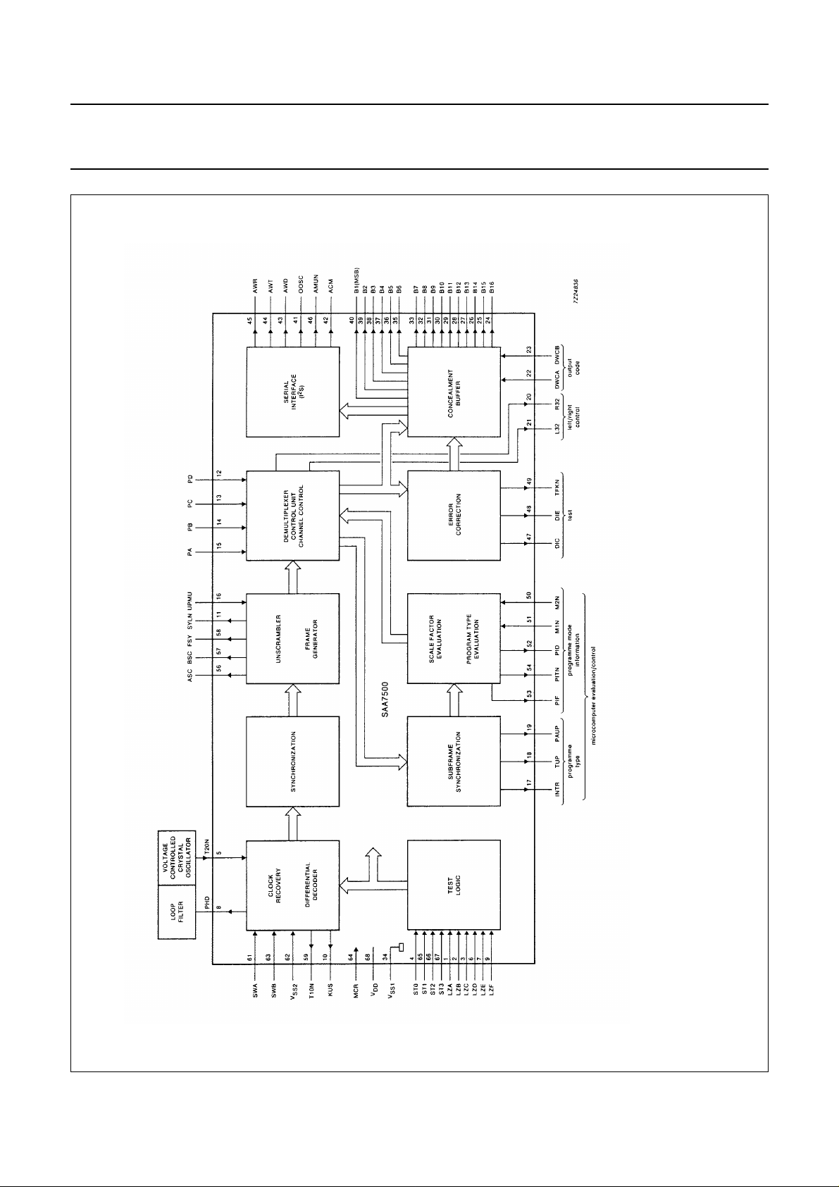
Fig.1 Block diagram.
Page 4
Philips Semiconductors Product specification
Digital satellite radio broadcasting tuner
decoder (SAT-2)
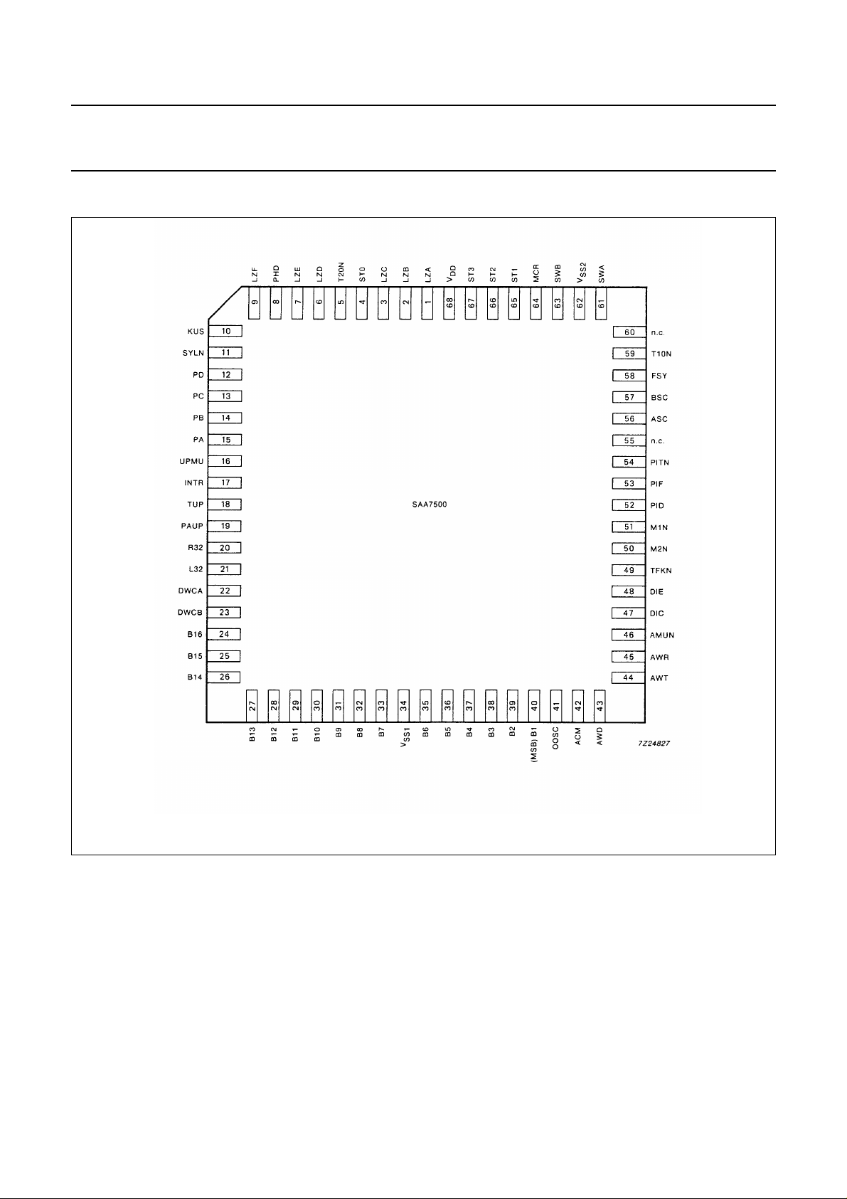
PINNING
SAA7500
Fig.2 Pinning diagram; for pin functions see next page.
September 1989 4
Page 5

Philips Semiconductors Product specification
Digital satellite radio broadcasting tuner
decoder (SAT-2)
Pin functions
(1) = CMOS level input. (2) = TTL level input. (3) = CMOS level input with pull down resistor.
PIN NO. MNEMONIC DESCRIPTION
1 LZA I(3) phase adjustment for the internal clock.
2 LZB I(3) phase adjustment for the internal clock.
3 LZC I(3) phase adjustment for the internal clock.
4 STO I(3) control input for testing.
5 T20N I(1) 20.48 MHz clock input from voltage controlled oscillator (VCX).
6 LZD I(3) control input for testing.
7 LZE I(3) control input for testing.
8 PHD O phase control signal for VCX.
9 LZF I(3) control input for testing.
10 KUS O test output (A’B’ swap).
11 SYLN O synchronization indication flag.
12 PD I(2) programme number input selector (MSB).
13 PC I(2) programme number input selector.
14 PB I(2) programme number input selector.
15 PA I(2) programme number input selector (LSB).
16 UPMU I(2) mute input (controlled by microcomputer).
17 INTR O interrupt flag for microcomputer.
18 TUP O programme type interface (clock).
19 PAUP O programme type interface (data).
20 R32 O multiplex control signal for right channel.
21 L32 O multiplex control signal for left channel.
22 DWCA I(3) DA-converter mode select input.
23 DWCB I(3) DA-converter mode select input.
24-33 B16-7 O audio data for parallel interface, bits 16 (LSB) to 7.
34 V
35-40 B6-1 O audio data for parallel interface, bits 6 to 1 (MSB).
41 OOSC O 4.096 MHz clock output.
42 ACM O concealment flag (for SAA7220P/C).
43 AWD O audio data (for SAA7220P/C).
44 AWT O bit clock (for SAA7220P/C).
45 AWR O word select signal (for SAA7220P/C).
46 AMUN O mute signal (for SAA7220P/C).
47 DIC O data output for testing.
48 DIE O data output for testing.
SS1
I ground (supply).
SAA7500
September 1989 5
Page 6

Philips Semiconductors Product specification
Digital satellite radio broadcasting tuner
SAA7500
decoder (SAT-2)
PIN NO. MNEMONIC DESCRIPTION
49 TFKN O burst clock for test data.
50 M2N I(2) channel mode select input.
51 M1N I(2) channel mode select input.
52 PID O programme information (PI) interface output (data).
53 PIF O programme information (PI) interface output (window signal).
54 PITN O programme information (PI) interface output (clock).
55 n.c. not connected.
56 ASC O data output for 10.24 Mbit/s interface.
57 BSC O data output for 10.24 Mbit/s interface.
58 FSY O window signal for 10.24 Mbit/s interface.
59 T10N O 10.24 MHz clock output.
60 n.c. not connected.
61 SWA I(2) 10.24 Mbit/s data input.
62 V
63 SWB I(2) 10.24 Mbit/s data input.
64 MCR I(1) master reset.
65 ST1 I(3) control input for testing.
66 ST2 I(3) control input for testing.
67 ST3 I(3) control input for testing and mode select for 10.24 Mbit/s interface.
68 V
SS2
DD
I ground (screen).
I power supply.
September 1989 6
Page 7

Philips Semiconductors Product specification
Digital satellite radio broadcasting tuner
SAA7500
decoder (SAT-2)
FUNCTIONAL DESCRIPTION
General
The SAA7500 has been designed to decode 16 stereo channel sound broadcasting signals in accordance with the
German standard - Technische Richtlinie ARD/ZDF Nr. 3R1. The channel carrying the sound broadcast programme
is selected and converted into an intermediate frequency by a frontend. The signal is then amplified and demodulated
(4 PSK (Phase Shift Keying) with carrier recovery). The outputs from the demodulator are two differential coded signals
that are input into the SAA7500. The SAA7500 decoder outputs the audio data, of the selected stereo or mono channel,
as linear quantized 16-bit audio samples.
Selection of the desired audio channel, as well as stereo or mono mode, is controlled by inputs PA, PB, PC and PD.
These inputs may be driven directly by switches or controlled by a microcomputer.
When under the control of a microcomputer, the SAA7500 transmits serial data to the microcomputer on the type of
programme (16 stereo or 32 mono). The corresponding synchronization of the subframe is partly performed by the
SAA7500 (every 2 ms) and at a higher level by the microcomputer (every 16 ms). The SAA7500 also sends to the
microcomputer, programme information code data together with its clock and window signal.
The circuit automatically performs the system error correction and concealment. In the transmit error rate range of 0 to
-3
3 ×10
transmit error rates ≤ 3 × 10⁻⁴.
The remaining functions, such as clock recovery, main and subframe synchronization and scale factor decoding, are
protected in a similar manner so that they will not influence the residual error rate.
a theoretical C/N (carrier-to-noise ratio) gain of about 6 dB is obtained. The residual error rate is nearly zero for
Clock recovery
The baseband signals A’ and B’ are connected to the SWA and SWB inputs of the SAA7500. For clock recovery, the
phase of the incoming data streams is compared with T10N (half the oscillator frequency). The output of the phase
comparator (PHD) controls, by means of the loop filter, the voltage controlled oscillator (both are external to the IC) and
thus its output signal T20N.
For energy dispersal, for example, in modulation pauses or with constant signals, the data streams are scrambled during
generation. The exceptions are the synchronization words and the special service bits. In order that the phase
correspondence between the recovered system clock (T10N) and the input signals A’ and B’ can be adjusted to a
minimum bit error rate (BER), a programmable phase shifter is provided (inputs LZA, LZB, LZC and ST3).
The differential decoder logic delivers the original data streams which may be exchanged depending on the number of
mixer stages on the transmission channel. The polarity of the two synchronization words will indicate if this is necessary,
if so the two data streams will be automatically switched over.
Synchronization
Using the synchronization circuit, the incoming data streams are first searched for 11-bit Barker codewords.
The synchronization circuit permits two errors for both synchronization words, which guards against failure of the
synchronization word. If the synchronization word has been detected, the following data is examined at frame length
intervals to see if the synchronization word is repeated. If it is repeated, it is acknowledged as a synchronization word
(window check) and an internal frame pulse generator takes over further control. There is also synchronization word
failure control which initiates a renewed synchronization word search and mutes the AF output if four successive
synchronization word failures occur.
To enhance the performance the result from the error correction circuit is used as an additional input to the
synchronization circuit. This is to avoid extra errors through synchronization loss in the case of relative high, but for
reception acceptable, bit error rates. This will not affect the rapid detection of a very high bit error rate or the
non-synchronization of the data stream. The decoder will function correctly with a bit error rate up to 3 × 10
-3
.
September 1989 7
Page 8

Philips Semiconductors Product specification
Digital satellite radio broadcasting tuner
SAA7500
decoder (SAT-2)
Demultiplexer
After synchronization, the beginning of a frame is marked and the digital signals are defined as to their assignment.
First the non-scrambled special service bit from the half frame A is taken out. The rest of both half frames are
unscrambled and demultiplexed so that each half frame is split into two substreams with a rate of 5.12 Mbit/s (see
Technische Richtlinie ARD/ZDF Nr. 3R1, main frame specification). Using the inputs from the synchronization circuit and
the programme selector (inputs PA, PB, PC and PD) the demultiplexer locks on to the selected programme block and
generates all the control signals required for further signal processing.
Error correction
The error correction circuit provides for exact identification of two errors in a 63/44 BCH block and correction of the
incorrect bits. In the event of more than two errors the identification circuit can identify incorrect BCH blocks with up to
five errors.
The BCH block is operated on by a syndrome calculator, the results controls the lines of an error correction matrix.
The output of this matrix corrects (inverts) the incorrect bits when data is shifted out from its buffer. The BCH block is
then fed through a second syndrome calculator. In the event of more than two errors the result of the whole calculation
will be other than zero. This information provides the concealment in the next stages.
The two adjacent samples related to the detected incorrect sample are added and divided by two, the result replaces the
incorrect sample (interpolation). In the event of successive bad samples the last corrected sample is held until a good
sample is detected (hold function). A high error frequency in the event of synchronization loss will activate the muting
function and set the output data to zero.
This information, if concealment is not active, is used in the synchronization circuit as described in that section.
When the samples are correct it can be assumed that the synchronization is also correct.
Scale factor, programme type evaluation and shift sunction
The transmitted samples are returned to their original range of values by the scale factor, which is obtained by decoding
the ZI-subframe. The start of this frame is coupled to the start of the special services frame, synchronization for this frame
uses the same principle as for the main frame. In the scale factor evaluation unit the BCH 14/6 code words (three times
transmitted) are fed into a majority selection circuit working at bit level. Subsequently the error check and the correction
of a maximum of two errors is carried out.
The SAA7500 contains the synchronization word detection and error check for the subframe synchronization word with
its repetition time of 2 ms. The programme type evaluation with its superior synchronization has to be performed external
to the chip, for example, by a microcomputer. For this purpose data is available in 8-bit blocks at a serial interface (INTR,
PAUP and TUP; block rate = 4000/s). The same microcomputer can also perform the programme selection (inputs PA,
PB, PC and PD).
At the input to the concealment buffer the corrected 11 bits (MSB) are combined with the 3 unprotected transmitted bits
(LSB). The scale factor determines the required shift-back operations needed to convert the transmitted values back into
the original values. Voids that occur are filled with noughts or ones corresponding to the sign bit. The shift-back and filling
of voids ensures that no incorrect bits occur above the range defined by the scale factor. The upper 16 bits represent the
regenerated audio sample.
September 1989 8
Page 9

Philips Semiconductors Product specification
Digital satellite radio broadcasting tuner
SAA7500
decoder (SAT-2)
Digital-to-analogue conversion and interfaces
The SAA7500 enables different DAC systems to be used. For control of the SAA7220P/C and TDA1541 a 2.5 external
divider must be connected to the 20.48 MHz clock signal to produce the required 8.192 MHz clock signal.
A serial interface is built in with the following outputs: bit clock (AWT), word select (AWR) and audio data (AWD).
In addition the mute signal (AMUN) and the concealment flag (ACM) are also available. The SAA7220P/C and TDA1541
are equipped with a digital audio interface for domestic use equivalent to ‘IEC proposal No. 84 (secretariat 28; from June
1985)’.
For DACs with a parallel interface in a multiplex mode the audio data are available at the B1(MSB)-B16 outputs.
The multiplexing is controlled by the L32 and R32 outputs. Using the mode outputs DWCA and DWCB the code (offset
binary or two’s complement) and polarity can be selected.
Additional information, including the scale factor is available through the programme information (PI) interface (PID,
PITN, and PIF). Another interface, using the ASC, BSC and T10N outputs, makes available signals from the differential
decoder. These signals are used for bit error measurement and an optimized phase adjustment of the internal clock (refer
to ‘clock recovery’ section).
An optional application of the control signals for mute and concealment operations is possible using the outputs AMUN
and ACM. For the mute signal a different time relationship to the unwanted pulse with very low C/N values may be
obtained.
The external application of the concealment signal is recommended; if an additional interpolation is required between
additional samples with different levels in the external circuitry (such as the SAA7220P/C).
Truth tables
Table 1 Delay adjustment
pins 1 to 3
LZC LZB LZA DELAY
0004× τ
0013× τ
0102× τ
0111× τ
1000× τ
101−1× τ
110−2× τ
111−3× τ
τ ≈ 1.5 × gate delay time (NAND)
Table 2 Master reset
pin 64
MCR FUNCTION
0 operation
1 master reset
Table 3 Mute
pin 16
UPMU FUNCTION
0no
1 yes
September 1989 9
Page 10

Philips Semiconductors Product specification
Digital satellite radio broadcasting tuner
decoder (SAT-2)
Table 4 Programme number
pins 12 to 15
PD PC PB PA PROGRAMME NO.
00001
00012
00103
.....
110114
111015
111116
Table 5 Phase control signal
pin 8
PHD PHASE
0 lead phase
1 lag phase
Table 6 Synchronization indication
pin 11
SYLN SYNCHRONIZATION
0 yes
1no
Table 7 Mode select for data outputs ASC and BSC for
10.24 Mbit/s interface
pin 67
SAA7500
Table 9 Channel mode select
pins 50 and 51
M2N M1N CHANNEL MODE
0 0 mono (1 + 2)
0 1 mono R(2)
1 0 mono L(1)
1 1 stereo
Table 10 Concealment
pin 42
ACM FUNCTION
0no
1 yes
Table 11 Mute
pin 46
AMUN MUTE
0 yes
1no
Table 12 Interrupt
pin 47
INTR INTERRUPT
0no
1 yes
ST3 DATA ASC/BSC
0 after unscrambler
1 before unscrambler
Table 8 Data converter mode select B1 (MSB) to B16
pins 22 and 23
DWCB DWCA DA CONVERTER MODE
0 0 compl. offset binary
0 1 offset binary
1 0 compl. 2’s complement
1 1 2’s complement
September 1989 10
Page 11

Philips Semiconductors Product specification
Digital satellite radio broadcasting tuner
decoder (SAT-2)
RATINGS
Limiting values in accordance with the Absolute Maximum Rating System (IEC 134)
PARAMETER SYMBOL MIN. MAX. UNIT
Supply voltage range V
Input voltage range
(1)
Input current I
Output current I
Supply current in V
Supply current in V
SS
DD
Total power dissipation P
Operating ambient temperature range T
Storage temperature range T
Note
1. V
+ 0.5 must not exceed 7.0 V.
DD
HANDLING
DD
V
I
I
O
I
SS
I
DD
tot
amb
stg
−0.5 7.0 V
−0.5 VDD+0.5 V
−± 10 mA
−± 10 mA
− 28 mA
− 28 mA
− 500 mW
−25 +85 °C
−55 +150 °C
SAA7500
Inputs and outputs are protected against electrostatic charge in normal handling, however, to be totally safe it is desirable
to take normal precautions appropriate to handling MOS devices (see Handling MOS Devices).
The PLCC-68 package can only be guaranteed with soldering temperatures up to a maximum of 235 °C.
September 1989 11
Page 12

Philips Semiconductors Product specification
Digital satellite radio broadcasting tuner
decoder (SAT-2)
DC CHARACTERISTICS
T
= 0 °C to + 70 °C; unless otherwise specified
amb
PARAMETER CONDITIONS SYMBOL MIN. TYP. MAX. UNIT
Supply voltage V
Supply current Fig.10 I
Quiescent supply current note 1 I
Inputs I(1)
Input voltage LOW V
Input voltage HIGH V
Input current LOW note 2 −I
Input current HIGH note 2 I
Inputs I(2)
Input voltage LOW V
Input voltage HIGH V
Input current LOW note 2 −I
Input current HIGH note 2 I
Inputs I(3)
Input voltage LOW V
Input voltage HIGH V
Pull down resistor R
Outputs O
Output voltage LOW −IOL = 1 mA V
Output voltage HIGH I
= 1 mA V
OH
DD
DD
DDq
IL
IH
IL
IH
IL
IH
IL
IH
IL
IH
I
OL
OH
SAA7500
4.5 − 5.5 V
− 12.5 − mA
−−50 µA
−−0.3 V
0.7 V
DD
−− V
DD
−−10 µA
−−10 µA
−−0.8 V
2.0 −− V
−−10 µA
− -10 µA
−−0.3 V
0.7 V
DD
−− V
DD
25 50 100 kΩ
−−0.5 V
4.0 −− V
V
V
Notes to DC characteristics
1. T
= 25 °C, all inputs at VSS or VDD, all outputs open.
amb
2. At 25 °C max. 1 µA.
September 1989 12
Page 13

Philips Semiconductors Product specification
Digital satellite radio broadcasting tuner
decoder (SAT-2)
AC CHARACTERISTICS
T
= 0 to + 70 °C; unless otherwise specified
amb
PARAMETER CONDITIONS SYMBOL MIN. TYP. MAX. UNIT
T20N clock pulse
Pulse width HIGH t
Pulse width LOW t
T20N pulse period t
Data input timing
Set-up time for data SWA and
SWB to T10N note 1 t
T10N pulse period T
PSW
Main frame timing
Main frame sync pulse t
Audio data timing
Audio sample repetition time t
Load pulse width HIGH t
Audio data hold t
2
S timing
I
Frequency AWT signal f
Audio sample repetition time t
PI interface timing
Frequency PITN signal f
PITN pulse period t
PIF pulse width HIGH t
PIF pulse period t
Output timing Programme type
interface
INTR pulse period t
INTR pulse width HIGH t
Fig.3
Fig.4
note 2 t
Fig.5
Fig.6
Fig.7
Fig.8
Fig.9
WH
WL
P20
SWL
P10
SYNC
SAMP
LPH
ADH
AWT
SAMP
PITN
PITN
PIFH
ZI
INTR
PINH
SAA7500
15 20 − ns
15 22 − ns
48 48.8 − ns
− 50 − ns
− 97.6 − ns
− 11t
P10
− 31.25 - µs
− 6.25 - µs
− 1- µs
− 1.024 − MHz
− 31.25 −µs
− 32 − kHz
− 31.25 −µs
− 22t
PITN
− 2 − ms
− 250 −µs
− 31.25 −µs
− ns
−µs
Notes to the characteristics
1. Due to noise, the period t
2. Due to noise, the period time t
may occasionally vary between 30 and 70 ns.
SWL
may occasionally vary between 77.6 and 117.6 ns.
PSW
September 1989 13
Page 14

Philips Semiconductors Product specification
Digital satellite radio broadcasting tuner
decoder (SAT-2)
Fig.3 Waveform at clock input T20N (pin 5).
SAA7500
Fig.4 Data input timing (pins 59, 61 and 63).
Fig.5 Output timing for 10.24 Mbit/s interface (pins 56, 57, 58 and 59).
September 1989 14
Page 15

Philips Semiconductors Product specification
Digital satellite radio broadcasting tuner
decoder (SAT-2)
SAA7500
Fig.6 Audio data timing parallel out (pins 40 to 35, 33 to 24, 21 and 20).
Fig.7 Inter-IC Sound (I2S) timing and mute and interpolation flags (pins 42 to 46).
September 1989 15
Page 16

Philips Semiconductors Product specification
Digital satellite radio broadcasting tuner
decoder (SAT-2)
Fig.8 PI interface timing (pins 52 to 54).
SAA7500
(1) Programme type - left
(2) Programme type - right
(3) This time is approximately 10 µs
Fig.9 Output timing programme type interface (pins 17 to 19).
September 1989 16
Page 17

Philips Semiconductors Product specification
Digital satellite radio broadcasting tuner
decoder (SAT-2)
SAA7500
Fig.10 Application proposal.
September 1989 17
Page 18

Philips Semiconductors Product specification
Digital satellite radio broadcasting tuner
decoder (SAT-2)
PACKAGE OUTLINE
PLCC68: plastic leaded chip carrier; 68 leads
e
y
61
68
1
pin 1 index
D
X
4460
43
SAA7500
SOT188-2
e
E
A
Z
E
b
p
b
1
w M
H
E
E
e
A
A
1
A
4
(A )
3
k
9
β
1
27
k
10 26
e
Z
D
H
D
D
v M
A
B
v M
B
0 5 10 mm
scale
DIMENSIONS (millimetre dimensions are derived from the original inch dimensions)
UNIT A
mm
inches
A
1
min. max. max. max. max.
4.57
0.51
4.19
0.180
0.020
0.165
A
0.25
0.01
A
4
3
3.30
0.13
b
0.53
0.33
0.021
0.013
b
p
1
0.81
0.66
0.032
0.026
D
24.33
24.13
0.958
0.950
(1)
(1)
E
eH
e
D
1.27
0.05
23.62
22.61
0.930
0.890
24.33
24.13
0.958
0.950
e
E
23.62
22.61
0.930
0.890
H
D
25.27
25.02
0.995
0.985
25.27
25.02
0.995
0.985
Note
1. Plastic or metal protrusions of 0.01 inches maximum per side are not included.
OUTLINE
VERSION
SOT188-2
IEC JEDEC EIAJ
112E10 MO-047AC
REFERENCES
k
1
k
E
1.22
1.07
0.048
0.042
0.51
0.020
L
1.44
1.02
0.057
0.040
detail X
p
EUROPEAN
PROJECTION
L
p
(1) (1)
Z
Z
E
D
ywv β
0.18 0.100.18
0.007 0.0040.007
2.16
0.085
2.16
0.085
o
45
ISSUE DATE
92-11-17
95-03-11
September 1989 18
Page 19

Philips Semiconductors Product specification
Digital satellite radio broadcasting tuner
decoder (SAT-2)
SOLDERING
Introduction
There is no soldering method that is ideal for all IC
packages. Wave soldering is often preferred when
through-hole and surface mounted components are mixed
on one printed-circuit board. However, wave soldering is
not always suitable for surface mounted ICs, or for
printed-circuits with high population densities. In these
situations reflow soldering is often used.
This text gives a very brief insight to a complex technology.
A more in-depth account of soldering ICs can be found in
our
“IC Package Databook”
Reflow soldering
Reflow soldering techniques are suitable for all PLCC
packages.
The choice of heating method may be influenced by larger
PLCC packages (44 leads, or more). If infrared or vapour
phase heating is used and the large packages are not
absolutely dry (less than 0.1% moisture content by
weight), vaporization of the small amount of moisture in
them can cause cracking of the plastic body. For more
information, refer to the Drypack chapter in our
Reference Handbook”
Reflow soldering requires solder paste (a suspension of
fine solder particles, flux and binding agent) to be applied
to the printed-circuit board by screen printing, stencilling or
pressure-syringe dispensing before package placement.
Several techniques exist for reflowing; for example,
thermal conduction by heated belt. Dwell times vary
between 50 and 300 seconds depending on heating
method. Typical reflow temperatures range from
215 to 250 °C.
(order code 9398 652 90011).
“Quality
(order code 9397 750 00192).
SAA7500
Preheating is necessary to dry the paste and evaporate
the binding agent. Preheating duration: 45 minutes at
45 °C.
Wave soldering
Wave soldering techniques can be used for all PLCC
packages if the following conditions are observed:
• A double-wave (a turbulent wave with high upward
pressure followed by a smooth laminar wave) soldering
technique should be used.
• The longitudinal axis of the package footprint must be
parallel to the solder flow.
• The package footprint must incorporate solder thieves at
the downstream corners.
During placement and before soldering, the package must
be fixed with a droplet of adhesive. The adhesive can be
applied by screen printing, pin transfer or syringe
dispensing. The package can be soldered after the
adhesive is cured.
Maximum permissible solder temperature is 260 °C, and
maximum duration of package immersion in solder is
10 seconds, if cooled to less than 150 °C within
6 seconds. Typical dwell time is 4 seconds at 250 °C.
A mildly-activated flux will eliminate the need for removal
of corrosive residues in most applications.
Repairing soldered joints
Fix the component by first soldering two diagonallyopposite end leads. Use only a low voltage soldering iron
(less than 24 V) applied to the flat part of the lead. Contact
time must be limited to 10 seconds at up to 300 °C. When
using a dedicated tool, all other leads can be soldered in
one operation within 2 to 5 seconds between
270 and 320 °C.
September 1989 19
Page 20

Philips Semiconductors Product specification
Digital satellite radio broadcasting tuner
SAA7500
decoder (SAT-2)
DEFINITIONS
Data sheet status
Objective specification This data sheet contains target or goal specifications for product development.
Preliminary specification This data sheet contains preliminary data; supplementary data may be published later.
Product specification This data sheet contains final product specifications.
Limiting values
Limiting values given are in accordance with the Absolute Maximum Rating System (IEC 134). Stress above one or
more of the limiting values may cause permanent damage to the device. These are stress ratings only and operation
of the device at these or at any other conditions above those given in the Characteristics sections of the specification
is not implied. Exposure to limiting values for extended periods may affect device reliability.
Application information
Where application information is given, it is advisory and does not form part of the specification.
LIFE SUPPORT APPLICATIONS
These products are not designed for use in life support appliances, devices, or systems where malfunction of these
products can reasonably be expected to result in personal injury. Philips customers using or selling these products for
use in such applications do so at their own risk and agree to fully indemnify Philips for any damages resulting from such
improper use or sale.
September 1989 20
 Loading...