

Page 1

INTEGRATED CIRCUITS
DATA SH EET
SAA7392
Channel encoder/decoder CDR60
Preliminary specification
File under Integrated Circuits, IC01
2000 Mar 21
Page 2

Philips Semiconductors Preliminary specification
Channel encoder/decoder CDR60 SAA7392
CONTENTS
1 FEATURES
2 GENERAL DESCRIPTION
3 QUICK REFERENCE DATA
4 ORDERING INFORMATION
5 BLOCK DIAGRAM
6 PINNING INFORMATION
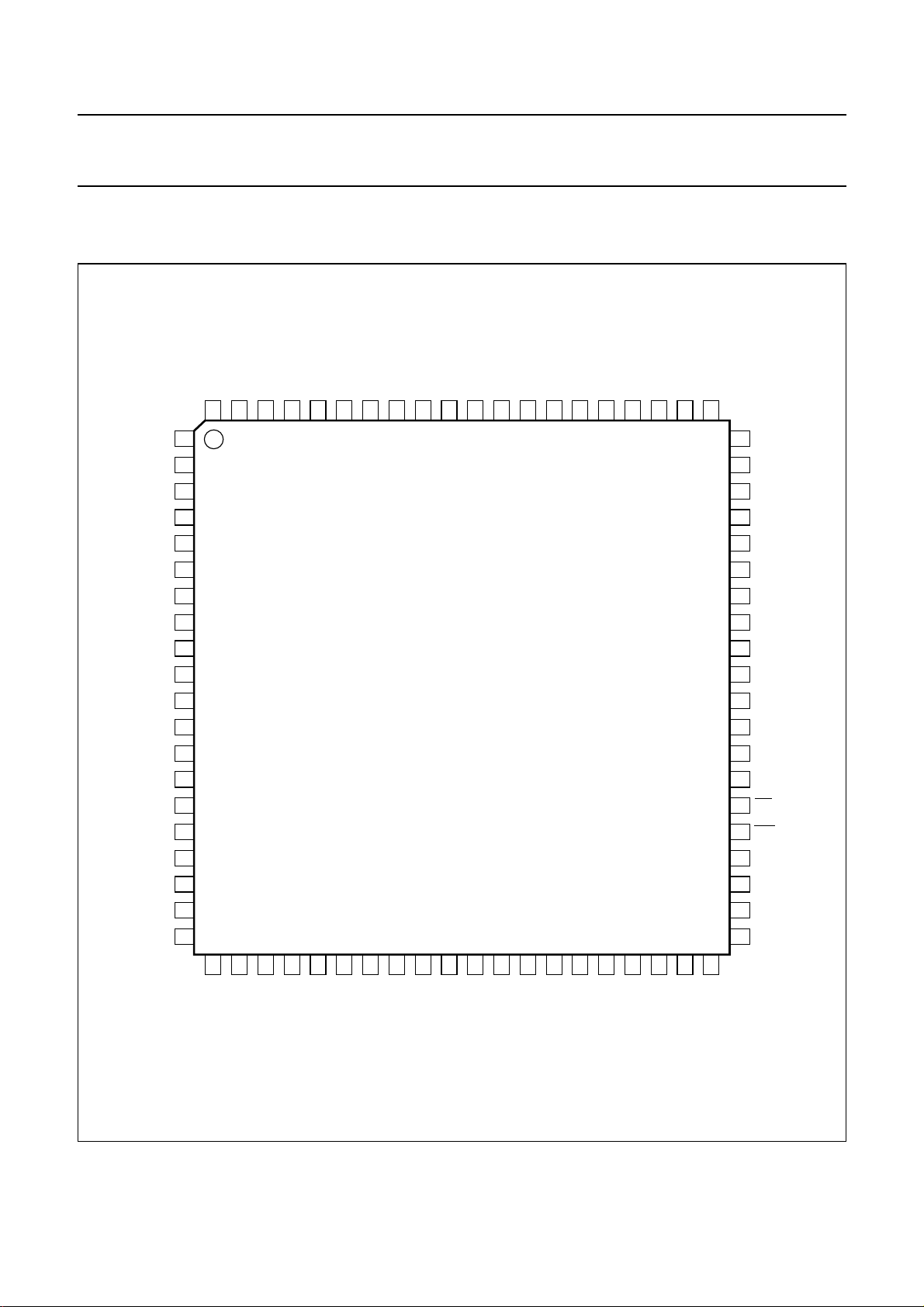
6.1 Pinning
6.2 Pin description
7 FUNCTIONAL DESCRIPTION
7.1 Microprocessor interfaces
7.2 Register map
7.3 System clocks
7.4 HF analog front-end
7.5 Bit recovery
7.6 Decoder function
7.7 Subcode interface
7.8 Digital output
7.9 Serial output interface
7.10 Motor control
7.11 The serial in function
7.12 The subcode insert function
7.13 The data encoder block
7.14 Encode control block
7.15 The EFM modulator
7.16 The EFM clock generator
7.17 The Wobble processor
8 LIMITING VALUES
9 OPERATING CHARACTERISTICS
9.1 ADC and AGC parameters
10 APPLICATION INFORMATION
10.1 Write startcontrol of encoder in CD-ROM mode
10.2 Write start control of encoder in Audio mode
10.3 Start-up of encode in flow-control operation
10.4 Start-up of encoder in synchronous stream
mode
10.5 Operating CDR60 in CAV mode, flow control
on input stream
10.6 Operating in CLV Mode, Flow Control on Input
Stream
10.7 Operating in CLV Mode, Synchronous Stream
Operation
11 PACKAGE OUTLINE
12 SOLDERING
12.1 Introduction to soldering surface mount
packages
12.2 Reflow soldering
12.3 Wave soldering
12.4 Manual soldering
12.5 Suitability of surface mount IC packages for
wave and reflow soldering methods
13 DEFINITIONS
14 LIFE SUPPORT APPLICATIONS
15 PURCHASE OF PHILIPS I2C COMPONENTS
2000 Mar 21 2
Page 3
Philips Semiconductors Preliminary specification
Channel encoder/decoder CDR60 SAA7392
1 FEATURES
• Very high speed Compact Disc (CD) compatible
decoding and encoding device
• On-chip Analog-to-Digital Converter (ADC) and
Automatic Gain Control (AGC) for HF data capture
• Eight-to-Fourteen Modulation (EFM)
• Advanced motor control loop to allow CAV, CLV and
pseudo-CLV playback
• Integrated FIFO for de-coupling of mechanism speed
and application speed
• Versatile output interface allowing different I2S-bus and
Electronic Industries Association of Japan (EIAJ)
formats
• Device is fully compatible with ELM, PLUM and Sanyo
CD-ROM block decoders
• Quad-pass CIRC correction for CD mode
(C1-C2-C1-C2)
• Subcode/header processing for CD format
• Frequency multiplier allows use of a 8 MHz crystal.
The bit detector recovers the individual bits from the
incoming signal, correcting asymmetry, performing noise
filtering and equalisation, and recovering the channel bit
clock using a digital PLL. The demodulator converts the
EFM bits to byte-wide data symbols, before passing them
onto the decoder for subcode extraction, de-interleaving
and error correction. The decoded data is then made
available via the multi-function serial output interface.
The encode datapath takes data symbols from the block
encoder/decoder via the serial data and subcode input
functions, encoding them via the encoder block. The
encoded data stream is passed to the EFM modulator,
which generates the required EFM signal, output as a
digital bitstream. Theencode process iscontrolled viathe
Wobble processor, encode control and EFM clock
generator functions.
2 GENERAL DESCRIPTION
As well as these two data processing sections, three
further blocks support overall device operation. The
CDR60 is a channel encoder/decoder for
CD/CD-R/CD-RW/CD Audio Recorder systems. It
incorporates all logic and RAM required for the complete
encoding and decoding processes.
There aretwo main datapathsthrough the CDR60 device.
system clockgenerator provides all digitalclocks required
by the CDR60. The motor servo allows the CDR60 to
control the spindle motor and is controlled by the
microprocessor interface. This interface can be accessed
either via a parallel (80C51) or a serial (I2C-bus) interface.
The decode datapath captures the incoming EFM data
stream via the HF ADC and AGC functions.
3 QUICK REFERENCE DATA
SYMBOL PARAMETER MIN. TYP. MAX. UNIT
V
V
V
I
f
T
T
DDD
DDA
DDE
DD
xtal
amb
stg
supply voltage (core and pad ring) 3.0 3.3 3.6 V
supply voltage (analog) 3.0 3.3 3.6 V
supply voltage (output drivers) 3.0 3.3 3.6 V
supply current − 200 − mA
crystal frequency 8 8.4672 33 MHz
operating ambient temperature 0 − 70 °C
storage temperature −55 − +125 °C
4 ORDERING INFORMATION
TYPE
NUMBER
NAME DESCRIPTION VERSION
PACKAGE
SAA7392HL LQFP80 plastic low profile quad flat package; 80 leads; body 12 × 12 × 1.4 mm SOT315-1
2000 Mar 21 3
Page 4

This text is here in white to force landscape pages to be rotated correctly when browsing through the pdf in the Acrobat reader.This text is here in
d
_white to force landscape pages to be rotated correctly when browsing through the pdf in the Acrobat reader.This text is here inThis text is here in
white to force landscape pages to be rotated correctly when browsingthrough the pdf inthe Acrobat reader. white to force landscape pages to be ...
2000 Mar 21 4
book, full pagewidth
5 BLOCK DIAGRAM
Philips Semiconductors Preliminary specification
Channel encoder/decoder CDR60 SAA7392
IREF
VREF
OTD
T1
T2
MOTO2/T3
MOTO1
V
SSA1
V
DDA1
V
DDA2
V
SSA2
V
DDD
V
SSD
V
DDE
8
IREF
7
GENERATOR
23
70
69
73
74
4
5
15
16
30, 49, 53, 76
19, 31, 43, 48,
52, 62, 71, 75
20, 44, 63, 72
WREFLO
HF DATA
CAPTURE
ATIPSYC
26
6
W441
25
WREFMID
WREFHI
3
1
PROCESSOR
WIN
2
WOBBLE
MOTOR/TACHO
INTERFACE
SAA7392
BIT DETECTOR DE-MODULATOR
SYSTEM CLOCK
GENERATOR
XEFM
78
EFM CLOCK
GENERATOR
RESET
EFMDATA
MODULATOR
TEST
CONTROL
PANIC
LASERON
79
EFM
ERROR CORRECTOR
AND
MEMORY PROCESSOR
77
ENCODE
CONTROL
SUB-CPU INTERFACE
27
SUBCODE
INSERT
SERIAL IN
SERIAL OUT
65
SUB
67
SFSY
66
RCK
64
DATAI
60
WCLK
61
BCLK
57
SYNC
55
V4
56
EBUOUT
59
DATAO
54
STOPCK
58
FLAG
51
PCAin
11
HREFLO
HREFMID
14
HREFHI
10
13
AGCREF
HIN
12
MEAS1
80
29
CL1
MUXSWI
24
XTLO
21
22
XTLI
28
PORE
Fig.1 Block diagram.
TEST2
18
17
TEST1
CFLG
35
to
42
DA7
to
DA0
47
ALE
68
RDi
45
46
WRi
CSi
32
50
SCL
SDA
34
33
MGR791
INT
Page 5
Philips Semiconductors Preliminary specification
Channel encoder/decoder CDR60 SAA7392
6 PINNING INFORMATION
6.1 Pinning
handbook, full pagewidth
WREFLO
WREFHI
WREFMID
V
SSA1
V
DDA1
WIN
VREF
IREF
n.c.
HREFHI
HREFLO
AGCREF
HIN
HREFMID
V
DDA2
V
SSA2
TEST1
TEST2
V
SSD
V
DDE
MEAS1
EFMDATA
XEFM
80
79
78
1
2
3
4
5
6
7
8
9
10
11
12
13
14
15
16
17
18
19
20
DDDVSSD
LASERON
V
77
76
75
MOTO1
74
MOTO2/T3
73
DDEVSSD
V
72
71
SAA7392
T1
70
T2
69
CFLG
68
SFSY
67
RCK
66
SUB
65
DATAI
64
DDEVSSD
V
63
62
BCLK
61
60
59
58
57
56
55
54
53
52
51
50
49
48
47
46
45
44
43
42
41
WCLK
DATAO
FLAG
SYNC
EBUOUT
V4
STOPCK
V
DDD
V
SSD
PCAin
CSi
V
DDD
V
SSD
ALE
RDi
WRi
V
DDE
V
SSD
DA0
DA1
21
22
23
24
25
26
27
28
29
30
XTLI
XTLO
OTD
W441
MUXSWI
PANIC
ATIPSYC
PORE
CL1
V
Fig.2 Pin configuration.
2000 Mar 21 5
DDD
31
SSD
V
32
SCL
33
SDA
34
INT
35
DA7
36
DA6
37
DA5
38
DA4
39
DA3
40
MGR792
DA2
Page 6

Philips Semiconductors Preliminary specification
Channel encoder/decoder CDR60 SAA7392
6.2 Pin description Table 1 LQFP80 package; note 1
SYMBOL PIN TYPE DESCRIPTION
WREFLO 1 O wobble ADC analog reference voltage
WREFHI 2 O wobble ADC analog reference voltage
WREFMID 3 O wobble ADC analog reference voltage
V
SSA1
V
DDA1
WIN 6 I wobble analog input
VREF 7 O analog voltage reference
IREF 8 O analog current reference
n.c. 9 − not connected
HREFHI 10 O HFADC analog reference voltage
HREFLO 11 O HF ADC analog reference voltage
AGCREF 12 I AGC analog reference voltage
HIN 13 I HF analog data input
HREFMID 14 O HFADC analog reference voltage
V
DDA2
V
SSA2
TEST1 17 I test input 1
TEST2 18 I test input 2
V
SSD
V
DDE
XTLI 21 I crystal oscillator input
XTLO 22 O crystal oscillator output
OTD 23 I off track detect input
MUXSWI 24 I clock multiplier enable
W441 25 O wobble 44.1 kHz clock output
ATIPSYC 26 O ATIPSync output
PANIC 27 I laser low power (LLP)
PORE 28 I power-on reset
CL1 29 O divided clock output
V
DDD
V
SSD
SCL 32 I sub-CPU clock
SDA 33 I/O bidirectional sub-CPU data
INT 34 O sub-CPU interrupt
DA7 35 I/O bidirectional sub-CPU parallel data bus
DA6 36 I/O bidirectional sub-CPU parallel data bus
DA5 37 I/O bidirectional sub-CPU parallel data bus
DA4 38 I/O bidirectional sub-CPU parallel data bus
4 supply analog ground
5 supply 3 V analog supply voltage 1; note 2
15 supply 3 V analog supply voltage 2; note 2
16 supply analog ground
19, 43, 62, 71 supply output driver ground
20 supply output driver 3 V supply voltage
30, 49, 53, 76 supply core and pad ring 3 V supply voltage; note 2
31, 48, 52, 75 supply core and pad ring ground
2000 Mar 21 6
Page 7
Philips Semiconductors Preliminary specification
Channel encoder/decoder CDR60 SAA7392
SYMBOL PIN TYPE DESCRIPTION
DA3 39 I/O bidirectional sub-CPU parallel data bus
DA2 40 I/O bidirectional sub-CPU parallel data bus
DA1 41 I/O bidirectional sub-CPU parallel data bus
DA0 42 I/O bidirectional sub-CPU parallel data bus
V
DDE
WRi 45 I sub-CPU write enable; active LOW
RDi 46 I sub-CPU read enable; active LOW
ALE 47 I sub-CPU address latch enable
CSi 50 I sub-CPU chip select
PCAin 51 I PCA input
STOPCK 54 O stop clock output
V4 55 O serial subcode output
EBUOUT 56 O digital output
SYNC 57 O I
FLAG 58 O I
DATAO 59 O I
WCLK 60 I/O bidirectional I
BCLK 61 I/O bidirectional I
V
DDE
DATAI 64 I I
SUB 65 I EIAJ subcode data
RCK 66 O EIAJ subcode clock
SFSY 67 I EIAJ subcode sync
CFLG 68 O correction statistics; open-drain
T2 69 I tacho control input 2
T1 70 I tacho control input 1
V
DDE
MOTO2/T3 73 I/O motor output 2/tacho input 3
MOTO1 74 O motor control output 1
LASERON 77 O laser write control
XEFM 78 O EFM clock output
EFMDATA 79 O EFM data output
MEAS1 80 O front end telemetry; open-drain
44 supply output driver 3 V supply voltage
2
S sector sync output
2
S correction flag
2
S data output
2
S word clock
2
S bit clock
63 supply output driver 3 V supply voltage
2
S data input
72 supply output driver 3 V supply voltage
Notes
1. No signal may be applied to this device when it is not powered.
2. The analog and digital supply pins (V
DDA
and V
) must be connected to the same external supply.
DDD
2000 Mar 21 7
Page 8
Philips Semiconductors Preliminary specification
Channel encoder/decoder CDR60 SAA7392
7 FUNCTIONAL DESCRIPTION
7.1 Microprocessor interfaces
The SAA7392 is programmed via two independent
microprocessor interfaces:
• Serial I2C-bus
– SDA=I2C-bus data
– SCL = I2C-bus clock
–I2C-bus write address = 3EH
–I2C-bus read address = 3FH.
• Parallel 80C51 compatible
– DA(7:0) = address/data bus
– ALE = address latch enable; latches the address
information on the bus
– WRi = active LOW write signal; write to SAA7392
– RDi = active LOW read signal; read from SAA7392
– CSi = chip select signal; gates the RDi and WRi
signals.
7.1.1 S
ERIAL I
C-BUS INTERFACE
2
Data is transferred over the interface in single bytes, via
write data or read data commands.
The sequence for a write data command is as follows:
1. Send START condition
2. Send address 3EH (write)
3. Write register address byte
4. Write data byte
5. Send STOP condition.
The sequence for a read data command is as follows:
1. Send START condition
2. Send address 3EH (write)
3. Write status register address byte
4. Send STOP condition
5. Send address 3FH (read)
6. Read data byte
7. Send STOP condition.
7.1.2 P
ARALLEL INTERFACE
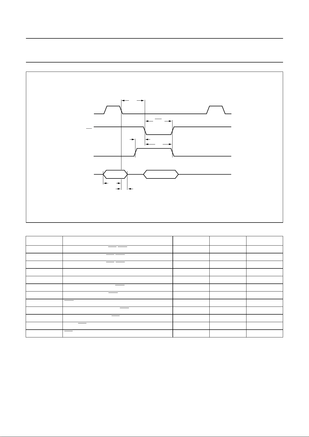
The parallelinterface hasa multiplexed address/databus.
Information can be written to or read from the SAA7392
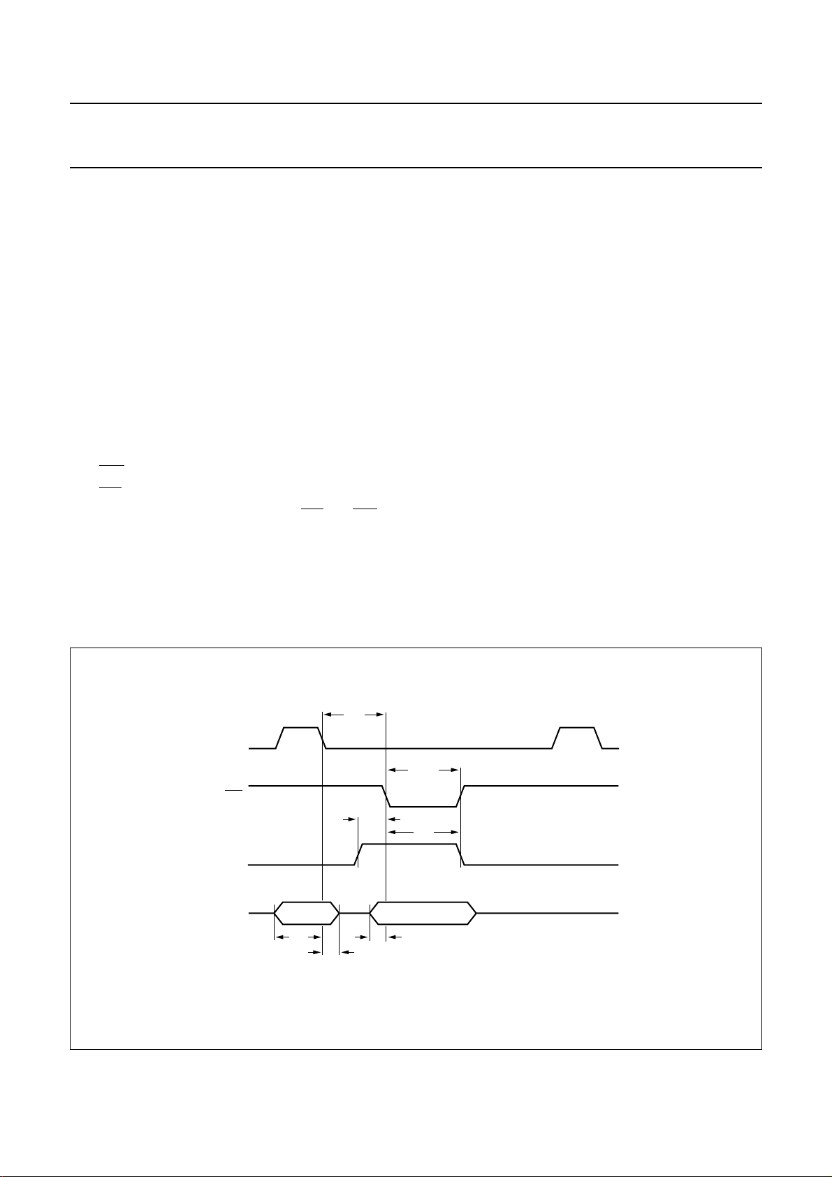
using the protocols shown inFigs 3 and 4; specific timings
are shownin Table 2. Notethat only thelower six address
bits are decoded; so writing to address 40H would have
the same effect as writing to address 00H.
t
handbook, full pagewidth
ALE
WRi
CSi
DA0 to DA7
address (0:7)
IN
t
su1
d1
t
d2
data (0:7)
t
t
h2
su2
Fig.3 Microprocessor write protocol.
2000 Mar 21 8
t
WRiL
t
IN
h1
MGR793
Page 9
Philips Semiconductors Preliminary specification
Channel encoder/decoder CDR60 SAA7392
t
handbook, full pagewidth
ALE
RDi
CSi
d1
RDi
L
t
d2
t
h1
DA0 to DA7
address (0:7)
IN
t
su1
t
h2
data (0:7)
OUT
Fig.4 Microprocessor read protocol.
Table 2 Parallel interface timing
SYMBOL DESCRIPTION MIN.
t
d1
t
d2
t
h1
t
su1
t
h2
t
su2
t
h3
t
WRiL
t
h4
t
d3
t
d4
t
RDiL
Delay ALE falling to RDi/WRi falling. 17 − ns
Delay CSi rising to RDi/WRi falling. 17 − ns
CSi hold time after RDi/WRi falling. 2T
Address setup time before ALE falling. 17 − ns
Address hold time after ALE falling. 17 − ns
Data setup time before WRi falling. 0 − ns
Data hold time after WRi falling. 2T
WRi LOW time. 1T
ALE LOW hold time after WRi LOW. 3T
Delay data valid after RDi LOW. − 3T
Delay RDi HIGH to data out high-impedance. − 17 ns
RDi LOW time. 3T
MGR794
(1)
+17 − ns
clk
+17 − ns
clk
+17 − ns
clk
+17 − ns
clk
+ 128 − ns
clk
(1)
MAX.
+17 ns
clk
UNIT
Note
1. T
is the system clock period.
clk
2000 Mar 21 9
Page 10

This text is here in white to force landscape pages to be rotated correctly when browsing through the pdf in the Acrobat reader.This text is here in
_white to force landscape pages to be rotated correctly when browsing through the pdf in the Acrobat reader.This text is here inThis text is here in
white to force landscape pages to be rotated correctly when browsingthrough the pdf inthe Acrobat reader. white to force landscape pages to be ...
2000 Mar 21 10
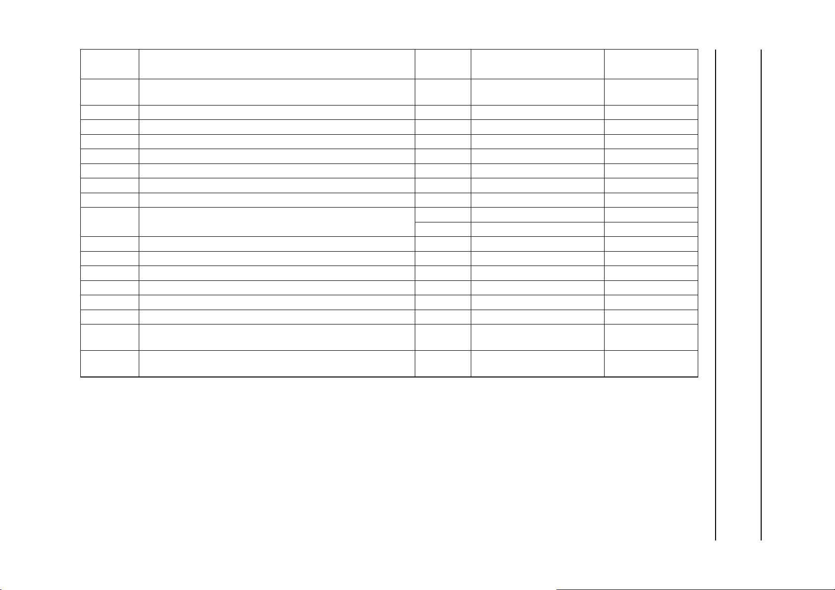
7.2 Register map Table 3 Register map
Philips Semiconductors Preliminary specification
Channel encoder/decoder CDR60 SAA7392
ADDRESS
(HEX)
00 PLL Lock Select Register (PLLLock) Write PLL lock select bit detector
01 PLL Bandwidth Select Register (PLLSet) Write PLL bandwidth select bit detector
02 PLL Frequency Preset Register (PLLFreq) Write PLL frequency preset bit detector
03 PLL Equalizer Preset Register (PLLEqu) Write PLL equalizer preset bit detector
04 PLL Lock Aid2 Preset Register (PLLFMeas) Write PLL lock aid 2 preset bit detector
05 I2S Output Register 1 (Output1) Write I2S output 1 serial out
06 I
07 I
08 Semaphore Register 1 (Sema1) Write/Read Inter-microprocessor
09 Semaphore Register 2 (Sema2) Write/Read Inter-microprocessor
0A Semaphore Register 3 (Sema3) Write/Read Inter-microprocessor
0B Interrupt Enable Register (IntEn) Write Enable interrupts sub-CPU
0B Status Register (Status) Read Interrupt status sub-CPU
0C Motor Control Register1 (Motor1) Write Frequency set-point motor/tacho
0D Motor Mode Select Register2 (Motor2) Write Motor coefficient preset motor/tacho
0E Motor Control Register 3 (Motor3) Write Motor integrator preset motor/tacho
0F Motor Control Register 4 (Motor4) Write Motor control motor/tacho
10 Motor Control Register 5 (Motor5) Read/Write Motor integrator value motor/tacho
11 Motor Control Register 6 (Motor6) Read/Write Motor integrator value motor/tacho
2
S Output Register 2 (Output2) Write I2S output 2 serial out
2
S Output Register 3 (Output3) Write I2S output 3 serial out
REGISTER NAME TYPE FUNCTION
Read 8-bit PLL frequency bit detector
Read 8-bit asymmetry signal bit detector
Read 8-bit jitter signal bit detector
Read Observe internal lock flags bit detector
communication
communication
communication
Read 8-bit slicer compensation
value
Read Opening of eye pattern bit detector
Read Read back of motor frequency motor/tacho
sub-CPU
sub-CPU
sub-CPU
bit detector
BLOCK
RESPONSIBLE
Page 11

This text is here in white to force landscape pages to be rotated correctly when browsing through the pdf in the Acrobat reader.This text is here in
_white to force landscape pages to be rotated correctly when browsing through the pdf in the Acrobat reader.This text is here inThis text is here in
white to force landscape pages to be rotated correctly when browsingthrough the pdf inthe Acrobat reader. white to force landscape pages to be ...
2000 Mar 21 11
ADDRESS
(HEX)
12 Clock Preset Register (ClockPre) Write Clock control clock generator
13 Decoder Mode Select Register (DecoMode) Write Decoder mode select encoder/decoder
14 Subcode Read End Register (SubReadEnd) Read Subcode data read finished encoder/decoder
15 Analog Settings Register 1 (AnaSet1) Write Analog control analog
16 Viterbi Detector Settings Register (VitSet) Write Viterbi detector control bit detector
17 Tacho Gain Setting Register (Tacho1) Write Tacho gain setting motor/tacho
18 Tacho Trip Setting Register (Tacho2) Write Tacho trip setting motor/tacho
19 Tacho Control Register (Tacho3) Write Tacho control settings motor/tacho
1B Soft Reset Register (SoftReset) Write Sub-block reset sub-CPU
1D Motor Control Register7 (Motor7) Write Control coefficients select motor/tacho
1E Input Configuration Register (InputConfig) Write EBU clock frequency and
20 Status Register 2 (Status2) Read/Write Interrupt status sub-CPU
21 Interrupt Enable Register 2 (IntEn2) Write Enable interrupts sub-CPU
22 Subcode Preset Count Register (SubPresetCount) Write Preset count field subcode insert
23 Subcode Configuration Register 1 (SubConfig1) Write Subcode control subcode insert
24 Subcode Configuration Register 2 (SubConfig2) Read/Write Subcode control subcode insert
25 Subcode Start Data Register (SubStartData) Write Subcode control subcode insert
26 Subcode Data Register (SubData) Read/Write Subcode data subcode insert
27 Wobble Configuration Register 1 (WobbleConfig1) Integrator and loop bandwidth Wobble processor
28 Wobble Configuration Register 2 (WobbleConfig2) Write Wobble PLL control Wobble processor
29 ATIP Status Register (ATIPStatus) Read ATIP status Wobble processor
2A Wobble Frequency Register 1 (WobbleFreq1) Read/Write 8 MSBs of PLL frequency Wobble processor
2B Wobble Frequency Register 2 (WobbleFreq2) Read/Write 8 LSBs of PLL frequency Wobble processor
2C ATIP Data Register (ATIPData) Read ATIP data Wobble processor
REGISTER NAME TYPE FUNCTION
Read Status of Q-channel subcode encoder/decoder
Read Q-channel subcode data encoder/decoder
Read C1 frames in FIFO + offset encoder/decoder
input format
Read Current count field subcode insert
Window width ATIP syncs Wobble processor
BLOCK
RESPONSIBLE
serial input
Philips Semiconductors Preliminary specification
Channel encoder/decoder CDR60 SAA7392
Page 12
This text is here in white to force landscape pages to be rotated correctly when browsing through the pdf in the Acrobat reader.This text is here in
_white to force landscape pages to be rotated correctly when browsing through the pdf in the Acrobat reader.This text is here inThis text is here in
white to force landscape pages to be rotated correctly when browsingthrough the pdf inthe Acrobat reader. white to force landscape pages to be ...
2000 Mar 21 12
ADDRESS
(HEX)
2D ATIP Data End Register (ATIPDataEnd) Read Least significant byte ATIP
2E Wobble Peak Status Register (WobbleStatus) Read Peak value of wobble signal Wobble processor
30 Encode WriteOn Control Register (EncodeWContr) Read/Write Laser and data flow control encode control
31 Encode Start Offset Register (EncodeStartOffset) Write Start WriteOn flags delay encode control
32 Encode Stop Offset Register (EncodeStopOffset) Write Stop WriteOn flags delay encode control
33 Encode Offset Register (EncodeXOffset) Write 10-bit value for Xoffset encode control
34 EFM Clock Configuration Register 1 (EFMClockConf1) Write EFM clock control EFM clock generator
35 EFM Clock Configuration Register 2 (EFMClockConf2) Write EFM clock control EFM clock generator
36 EFM Clock Configuration Register 3 (EFMClockConf3) Write EFM clock control EFM clock generator
37 EFM PLL Frequency Register (EFMPLLFreq) Read EFM PLL frequency EFM clock generator
37 EFM Clock Configuration Register 4 (EFMClockConf4) Write EFM clock control EFM clock generator
38 ATIP Error Register (ATER) Read Counter for ATIP CRC errors sub-CPU
39 C1 Block Error Register (C1BLER) Read Counter for C1 errors sub-CPU
3A C2 Block Error Register (C2BLER) Read Counter for C2 errors sub-CPU
3C EFM Preset Count Register (EFMPresetCount) Write EFM frame position for output EFM modulator
3D EFM Modulator Configuration Register (EFMModConfig) Write XEFM control and output data
3E EFM Modulator Configuration Register 2 (EFMModConfig2) Write XEFM control and output data
REGISTER NAME TYPE FUNCTION
data
Read Integrator value EFM clock generator
format
format
BLOCK
RESPONSIBLE
Wobble processor
EFM modulator
EFM modulator
Philips Semiconductors Preliminary specification
Channel encoder/decoder CDR60 SAA7392
Page 13

Philips Semiconductors Preliminary specification
Channel encoder/decoder CDR60 SAA7392
7.2.1 INTERRUPT PIN
The interrupt pin (INT) is the AND-OR-INVERT of the Status and Interrupt Enable Registers, i.e. INT will become active
when corresponding bits are set at the same time in the Status and Interrupt Enable Registers.
7.2.2 THE SEMAPHORE REGISTERS (SEMA1, SEMA2 AND SEMA3)
The Semaphore Registers are intended for inter-microprocessor communications. For example, microcontroller 1 can
writedata tomicrocontroller 2 viaSema1 andmicrocontroller 2 can writedata tomicrocontroller 1 viaSema2. TheStatus
Register ofthe SAA7392offers a mechanismso that both microcontrollers cansee when newdata hasbeen written and
whenit hasbeen readby lookingat thecontents ofthe Semaphore Registers. Version M3of theCDR60 canbe identified
by writingand reading register Sema3. In version M3,bit 1 of Sema3is always read as logic 0, whereas inother CDR60
versions this bit reads the same value as what was written to it before.
7.2.2.1 Semaphore Register 1 (Sema1)
Table 4 Semaphore Register 1 (address 08H) - READ/WRITE
76543210
Sema1.7 Sema1.6 Sema1.5 Sema1.4 Sema1.3 Sema1.2 Sema1.1 Sema1.0
7.2.2.2 Semaphore Register 2 (Sema2)
Table 5 Semaphore Register 2 (address 09H) - READ/WRITE
76543210
Sema2.7 Sema2.6 Sema2.5 Sema2.4 Sema2.3 Sema2.2 Sema2.1 Sema2.0
7.2.2.3 Semaphore Register 3 (Sema3)
Table 6 Semaphore Register 3 (address 0AH) - READ/WRITE
76543210
Sema3.7 Sema3.6 Sema3.5 Sema3.4 Sema3.3 Sema3.2 Sema3.1 Sema3.0
7.2.3 S
Table 7 Status Register (address 0BH) - READ
Table 8 Description of Status bits
TATUS REGISTER (STATUS)
76543 210
Sema1 Sema2 Sema3 LockIn HeaderVal MotorOverflow FIFOOv −
BIT SYMBOL DESCRIPTION
7 Sema1 If Sema1 = 1, change in register Sema1 has been detected. Reset if register Sema1 read.
6 Sema2 If Sema2 = 1, change in register Sema2 has been detected. Reset if register Sema2 read.
5 Sema3 If Sema3 = 1, change in register Sema3 has been detected. Reset if register Sema3 read.
4 LockIn If LockIn = 1, then channel data PLL in lock (not latched).
3 HeaderVal HeaderVal is set when new header/subcode is available; reset on reading SubReadEnd.
2 MotorOverflow If MotorOverflow = 1, then a motor overflow is occurring (not latched).
1 FIFOOv If FIFOOv = 1, then the FIFO has overflowed.
0 − This bit is reserved.
2000 Mar 21 13
Page 14

Philips Semiconductors Preliminary specification
Channel encoder/decoder CDR60 SAA7392
7.2.4 INTERRUPT ENABLE REGISTER (INTEN)
Table 9 Interrupt Enable Register (address 0BH) - WRITE
76543 2 10
Sema1En Sema2En Sema3En LockInEn HeaderValen MotorOverflowEn FIFOOvEn −
Table 10 Description of IntEn bits
BIT SYMBOL DESCRIPTION
7 Sema1En If Sema1En = 1, then Semaphore Register 1 interrupt is enabled.
6 Sema2En If Sema2En = 1, then Semaphore Register 2 interrupt is enabled.
5 Sema3En If Sema3En = 1, then Semaphore Register 3 interrupt is enabled.
4 LockInEn If LockinEn = 1, then channel data PLL in lock interrupt is enabled.
3 HeaderValEn If HeaderValEn = 1, then new header/subcode available interrupt is enabled.
2 MotorOverflowEn If MotorOverflowEn = 1, then motor overflow interrupt is enabled.
1 FIFOOvEn If FIFOOvEn = 1, then FIFO overflow interrupt is enabled.
0 − This bit is reserved.
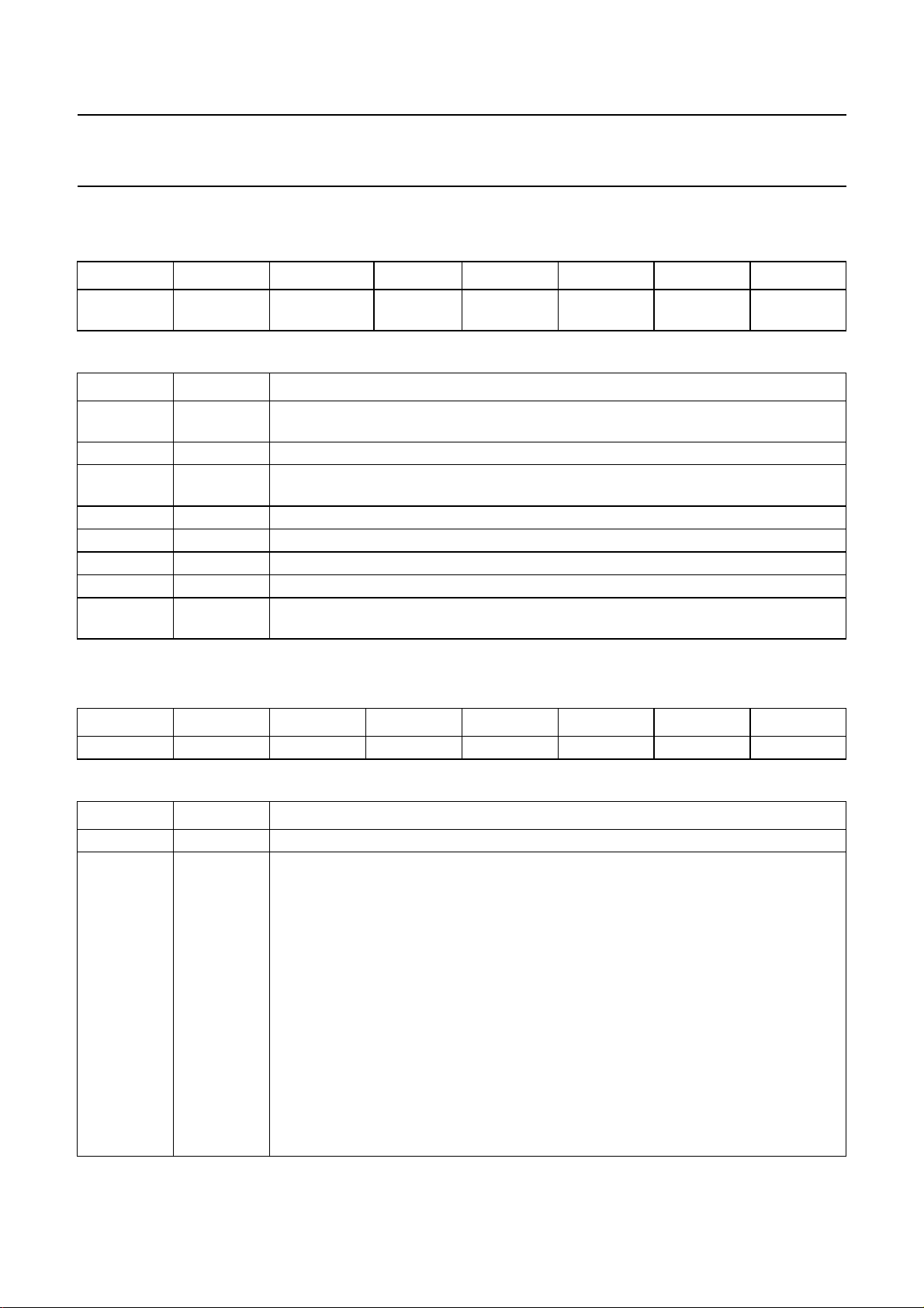
7.2.5 S
Table 11 Status Register 2 (address 20H) - READ/WRITE
BankSwitch SyncError DataNotValid QSync ATIPSync LaserOn LaserOff XErrorLarge
Table 12 Description of Status2 bits
BIT SYMBOL DESCRIPTION
TATUS REGISTER 2(STATUS2)
76 543210
7 BankSwitch When set a ‘Bank switch’in the subcode insert blockhas occurred; reset when a logic 1
is written to this bit.
6 SyncError When set synchronisation with PLUM on subcode transfer has failed; reset when a
logic 1 is written to this bit.
5 DataNotValid When set an under-run on subcode transfer with PLUM has occurred; reset when a
logic 1 is written to this bit.
4 QSync When set a Q-channel subcode sync has been written to disc; reset when a logic 1 is
written to this bit.
3 ATIPSync When set sync has been found in the ATIP channel; reset when a logic 1 is written to
this bit.
2 LaserOn When set a rising edge of the internal LaserOn signal has occurred; reset when a
logic 1 is written to this bit.
1 LaserOff When set a falling edge of the internal LaserOn signal has occurred; reset when a
logic 1 is written to this bit.
0 XErrorLarge Whenset the offset between QSync and ATIPSync is more than 2 EFM frames different
from the programmed value.
2000 Mar 21 14
Page 15
Philips Semiconductors Preliminary specification
Channel encoder/decoder CDR60 SAA7392
7.2.6 INTERRUPT ENABLE REGISTER 2(INTEN2)
Table 13 Interrupt Enable Register 2 (address 21H) - WRITE
76 543210
BankSwitchEnSyncErrorEn DataNotValidEnQSyncEn ATIPSyncEn LaserOnEn LaserOffEn XErrorLarge
En
Table 14 Description of IntEn2 bits
BIT SYMBOL DESCRIPTION
7 BankSwitchEnIf BankSwitchEn = 1, then BankSwitch interrupt is enabled.
6 SyncErrorEn If SyncErrorEn = 1, then SyncError interrupt is enabled.
5 DataNotVali
dEn
4 QSyncEn If QSyncEn = 1, then QSync interrupt is enabled.
3 ATIPSyncEn If ATIPSyncEn = 1, then ATIPSync interrupt is enabled.
2 LaserOnEn If LaserOnEn = 1, then LaserOn interrupt is enabled.
1 LaserOffEn If LaserOffEn = 1, then LaserOff interrupt is enabled.
0 XErrorLargeEnIf XerrorLarge = 1, then XErrorLarge interrupt is enabled.
If DataNotValidEn= 1, then DataNotValid interrupt is enabled.
7.2.7 S
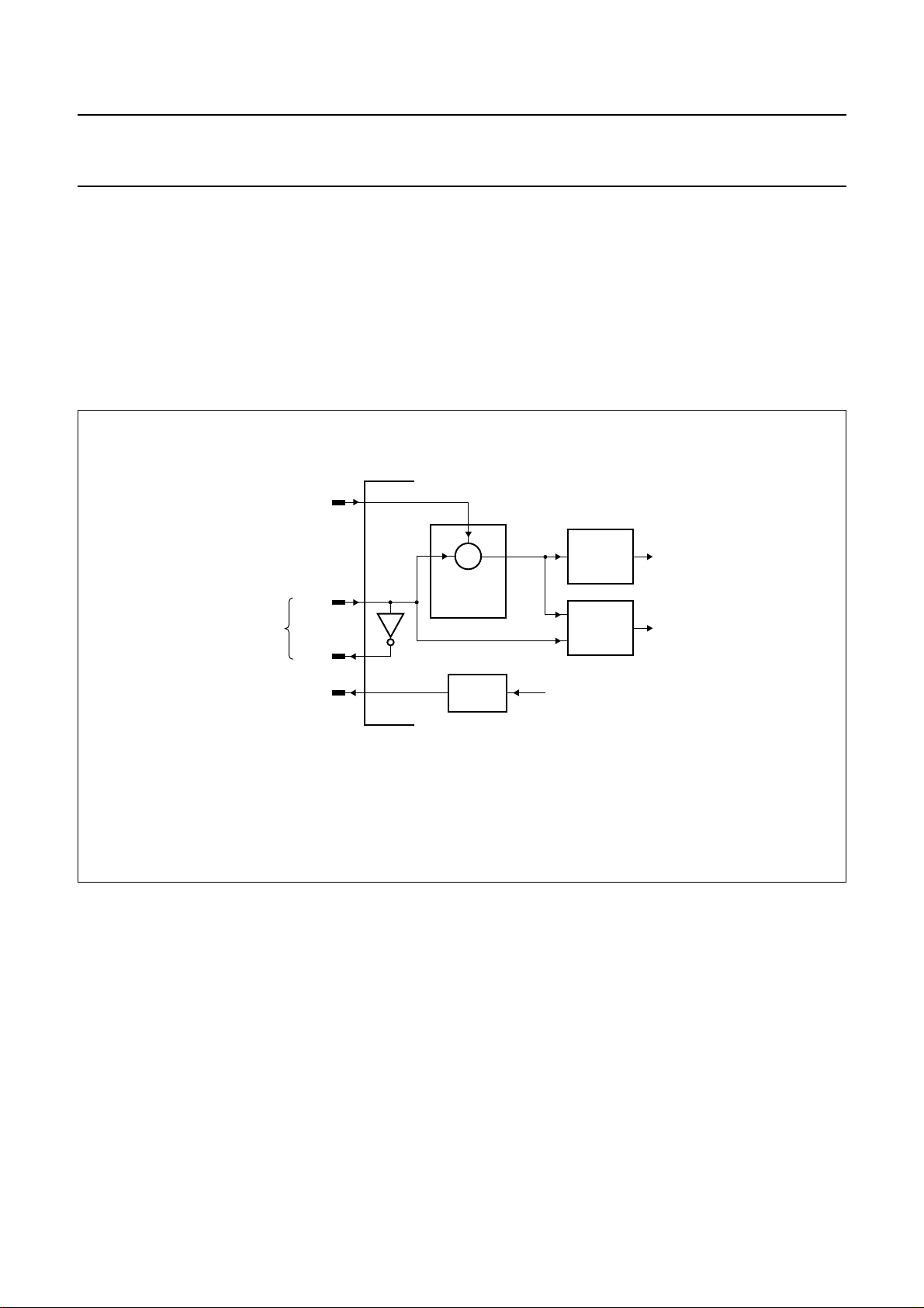
Table 15 Soft Reset Register (address 1BH) - WRITE
Table 16 Description of SoftReset bits
OFT RESET REGISTER (SOFTRESET)
76543210
−−−−−−−SReset1
BIT SYMBOL DESCRIPTION
7to1 − These 7 bits are reserved.
0 SReset1 When set, synchronisation with PLUM on subcode transfer has failed; reset when
a logic 1 is written to this bit (Status2).
This bit is an active HIGH reset to the following blocks: Encoder/decoder, EFM
modulator, Encode control block, Serial input/output block and Encode subcode insert
block. The clock control, EFM PLL, tacho, motor interface and wobble interface remain
running.
Soft reset will reset the following registers: EFMPresetCount, EFMModulateConfig,
EFMModulateConfig2, EncodeXOffset, EncodeWriteControl, EncodeStartOffset,
EncodeStopOffset, SubPresetCount, SubConfig1, Subconfig2,SubStartData, SubData,
InputConfig, DecoMode, Output1, Output2 and Output3.
A soft reset is mandatory in the following cases:
1. After programming the BCLK clock
2. When switching from encode to decode
3. When switching from decode to encode.
2000 Mar 21 15
Page 16
Philips Semiconductors Preliminary specification
Channel encoder/decoder CDR60 SAA7392
7.3 System clocks
The principleclocks used inthe SAA7392 are derived from the crystaloscillator input pinXTLI (alternatively, anexternal
clock can be connected to this pin). These clocks are the system clock (also used as the ADC clock) and the I2S output
bit clock (BCLK).
The system clock (f
) defines the maximumoperational channel rate for the device. The maximum EFM channel clock
clk
is twice the system clock, for CD it is equivalent tosystem clock/(4.3 × 106) which is approximately 11.5 × CDROM for a
25 MHz system clock.
The other clock in the system is the channel data clock, this is recovered by the front-end bit recovery PLL.
handbook, full pagewidth
crystal
oscillator
MUXSWI
XTLI
XTLO
CL1
×
(1)
CLOCK
MULTIPLIER
CL1
DIVIDER
M × XTLI
XTLI
SYSTEM
CLOCK
DIVIDER
BIT
CLOCK
DIVIDER
system clock
system clock
BCLK
MGR795
(1) M = 1 if MUXSWI is LOW; M = 8 if MUXSWI is HIGH.
Fig.5 System clock generator.
2000 Mar 21 16
Page 17

Philips Semiconductors Preliminary specification
Channel encoder/decoder CDR60 SAA7392
7.3.1 CLOCK PRESET REGISTER (CLOCKPRE)
Table 17 Clock Preset Register (address 12H) - WRITE
76543210
CL1Div GateBClk Div.1 Div.0 Mux2 Div2.2 Div2.1 Div2.0
Table 18 Description of ClockPre bits
BIT SYMBOL DESCRIPTION
1
⁄3f
7 CL1Div If CL1Div = 0, then CL1 output frequency is
frequency is1⁄2f
6 GateBClk If GateBClk = 0, then I
clk
.
2
S output bit clock gating is disabled. If GateBClk = 1, then I2S
output bit clock gating enabled, BCLK is output, clock is automatically stopped if FIFO
underflows (this is known as Flow control mode).
5 Div.1 These 2 bits select the system clock frequency (f
4 Div.0
should be programmed for the expected disc channel rate (e.g. 4.33 MHz for 1 × CD)
within the following constraints:
. If CL1Div = 1, then CL1 output
clk
); see Table 19. This frequency
clk
Channel rate
---------------------------------2
4 Channel rate×<<
f
clk
In this clock range, reliable bit detection is possible. All data found will be written to the
FIFO. It is the responsibility of the user to select system clock values so that the FIFO
performance is controlled.
3 Mux2 If Mux2 = 0, then N (bit clock divider pre-scaler) = 1. If Mux2 = 1, then N = M.
2 to 0 Div2<2:0> These 3 bits select the BCLK frequency (f
); see Table 20. It is the responsibility of
BCLK
the user to select BCLK values so that the FIFO performance is controlled.
Table 19 Selection of system clock frequency
Div.1 Div.0 SYSTEM CLOCK FREQUENCY (f
00M×f
0 1 0.5 × M × f
1 0 0.25 × M × f
1 1 0.125 × M × f
XTLI
XTLI
XTLI
XTLI
clk
Table 20 Selection of BCLK frequency
Div2.1 Div2.1 Div2.0 BCLK FREQUENCY (f
000N×f
001N×f
010
011
100
101
110
111
XTLI
XTLI
1
/
(N × f
2
1
/
(N × f
3
1
/
(N × f
4
1
/
(N × f
6
1
/
(N × f
8
1
/
(N × f
12
XTLI
XTLI
XTLI
XTLI
XTLI
XTLI
)
)
)
)
)
)
BCLK
)
)
2000 Mar 21 17
Page 18
Philips Semiconductors Preliminary specification
Channel encoder/decoder CDR60 SAA7392
7.4 HF analog front-end
The HF ADC in the SAA7392 encodes the EFM high
frequency signal from the disc light pen assembly. These
signals are pre-processed, externally to the SAA7392, by
either AEGER-2 or a DALAS equivalent. The dynamic
range of the ADC is optimized by the inclusion of an
AC coupled AGC function under digital control.
In order to make use of the whole digital front-end
resolution, the output of the gain control amplifier should
constantly deliver 1.4 V
ofthe ADC isapproximately14 dB, with32 steps. Thegain
control for the variable gain amplifier is controlled by an
on-chip digital gaincontrol block (AGC). This blockallows
for both automatic and microprocessor gain control. The
gain control block will detect ADC extreme conditions
(00H or FFH outputs); on these values the gain control
block will decrement the gain. If no extreme codes occur
the gain is incremented.
7.4.1 FIXED GAIN
Control of the gain is as follows:
1. Writing XX1X XXXX to the Anaset1 register
(address 15H) increases the AGC gain by 1.1 dB
2. Writing XX0X XXXX to the AnaSet1 register
(address 15H) decreases the AGC gain by 1.1 dB
output signal. The gain range
(p-p)
3. Instructions to increment/decrement gain are ignored
when the AGC gain limits of −4/+12 dB are reached.
7.4.2 AUTOMATIC GAIN CONTROL (AGC)
The gain of theAGC cellis adjusteduntil the analog signal
at the ADC input extends over the complete range of
the ADC.Detection ofthis conditionis in thedigital domain
where the maximum and minimum ADC codes are
measured. The dynamics of the AGC system are as
follows.
1. If the ADC output codes are not full scale (i.e.
000 0000 and 111 11111) the AGC gain is
incremented in 1.1 dB steps with a time constant of
1000/n µs, where n is the over-speed factor i.e. n = 1
for basic audio CD.
2. When full scale is detected at the output of the ADC
the AGC gain is fixed provided that full scale is
maintained and clipping does not occur for greater
than 20% of the time.
3. If clipping occurs for more than 20% of the time, then
the AGC gain is reduced in 1.1 dB steps with a time
constant of 60/n µs.
The ADC and AGC electrical characteristics are specified
in Chapter 9.
7.4.3 ANALOG SETTINGS REGISTER 1(ANASET1)
Table 21 Analog Settings Register 1 (address 15H) - WRITE
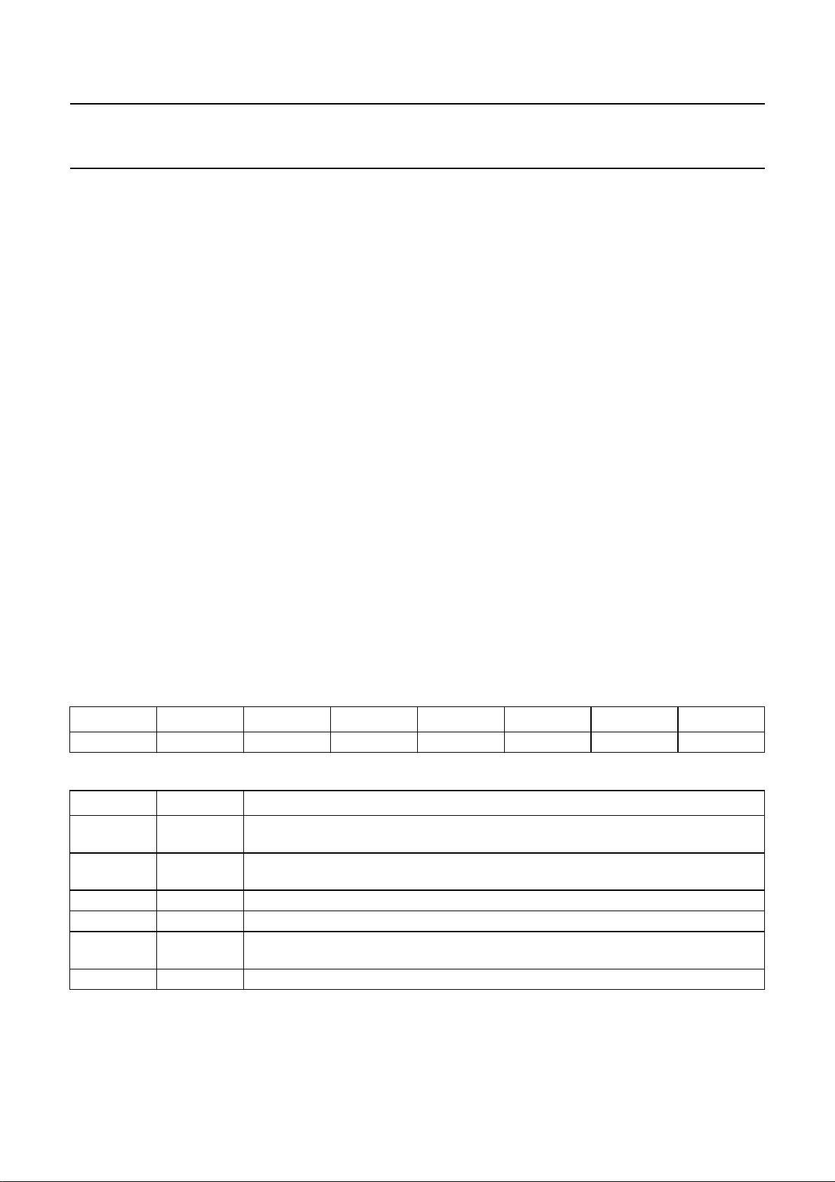
76543210
GainControl MaxGain StepUp StepDown PowerDown −−−
Table 22 Description of AnaSet1 bits
BIT SYMBOL DESCRIPTION
7 GainControl If GainControl = 0, then gain control is in Hold mode. If GainControl = 1, then automatic
gain control is on.
6 MaxGain If MaxGain = 0, then there is no gain limit. If MaxGain = 1, then the maximum gain is
7.66 dB.
5 StepUp If StepUp = 1, then step up gain by one LSB.
4 StepDown If StepDown = 1, then step down gain by one LSB.
3 PowerDown If PowerDown = 0, then analog blocks are powered up. If PowerDown = 1, then analog
blocks are powered down.
2to0 − These 3 bits are reserved and must be set to a logic 0s.
2000 Mar 21 18
Page 19

Philips Semiconductors Preliminary specification
Channel encoder/decoder CDR60 SAA7392
7.5 Bit recovery
The bit recovery block (shown in Fig.6) contains the slice
levelcircuitry, anoise filtertolimit theHF-EFMsignal noise
contribution, an adaptive slicer circuit and a digital PLL.
These blocks can be controlled via the microprocessor.
The channel rate should always obey the following
constraints:
• It should be less than 2 × the system clock
• It should be greater than 0.25 × the system clock.
In this clock range reliable bit clock detection is possible.
All data found will be written to the FIFO. It is the
responsibility ofthe user toselect BCLK and system clock
values so that the FIFO operation is controlled.
The digital noise filter runs on the PLL bit clock and limits
the bandwidthof the incomingsignal to 0.25 ofthe PLL bit
clock frequency. The characteristics of the filter are:
• Passband: 0 to 0.22 f
• Stopband: 0.28 fb to (f
b
− 0.28 fb)
clk
• Rejection: −28 dB.
The slice level determination circuit compensates the
incoming signalasymmetry component. Thebandwidth of
this circuit is programmable via register PLLSet.
A programmable (one tap presetable, asymmetrical)
equaliser is used in the bit detection circuit. The first and
last tap settings are different. Possible tap values are
settable via register PLLEqu.
The advanced detector has two extra detection circuits
(adaptive slicer and run length 2 push-back) which are
controlled via the VitSet register, that allow improved
margin in the bit detector.
The adaptive slicer does a second stage slice operation;
thebandwidth ishigherthan thefirst slicer. Itcan beturned
on/off via the VitSet register.
If the advanced detector is switched on all run length 2
symbols are pushed back to run length 3. The circuit will
determine thetransition that was most likely to bein error,
and shift the transition on that edge.
GAIN CONTROLLED
handbook, full pagewidth
AMPLIFIER
HIN
GAIN CONTROL
BLOCK
ADC
+
+
−
NOISE
FILTER
SLICE LEVEL
DETERMINE
DIGITAL
EQUALIZER
clocked on PLL clock
DIGITAL
PLL
RMS JITTER
MEASUREMENT
Fig.6 Block diagram of bit recovery block.
VITERBI
DETECTOR
ZERO TRANS
DETECTOR
PLL frequency
jitter value
slice level
MULTIPLEXER
MEAS1
MGR796
2000 Mar 21 19
Page 20
Philips Semiconductors Preliminary specification
Channel encoder/decoder CDR60 SAA7392
7.5.1 DIGITAL PLL
The digital PLL will recover the channel bit clock. As the
capturerange ofthe PLLitselfis limited,lockdetectors and
2 capture aids are present. In total three different PLL
operation modes exist: In-lock, Inner-lock aid and
Outer-lock aid.
The PLL behaviour during in-lock (the normal on-track
situation) can be best explained in the frequency domain.
The PLL operation is completely linear during in-lock
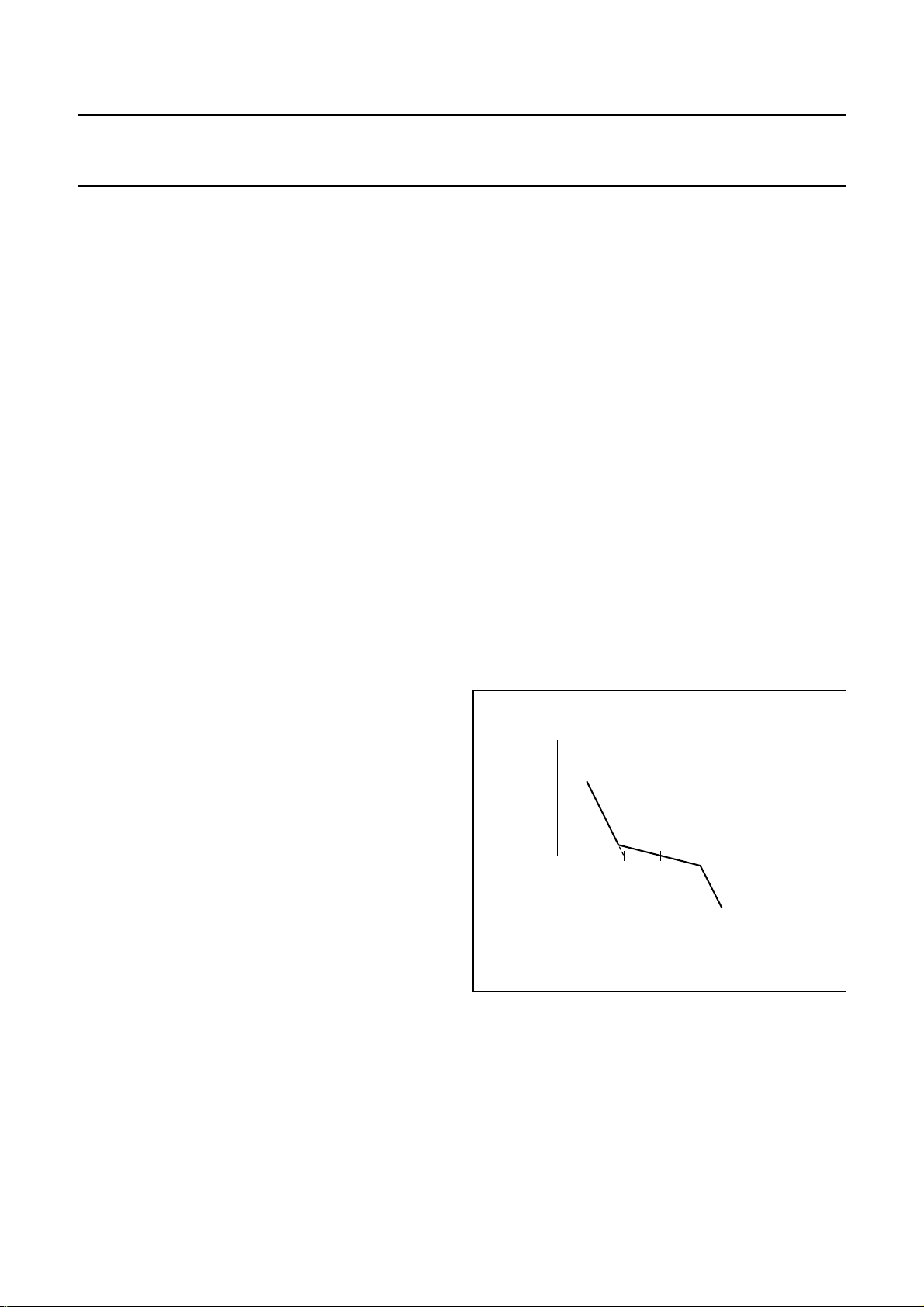
situations. The open-loop response of the PLL is given in
Fig.7. The three frequencies, f0(integrator cross-over
frequency), f1(PLL bandwidth) and f2(low-pass
bandwidth) are programmable via register PLLSet.
To extend the PLL capture range two lock aids are used:
• Inner lock aid: has a capture range of ±10% and will
bring the PLL frequency to the lock point
• Outer lock range: has no limitation on capture range,
and will bring the PLL within the range of the inner lock
range.
Two outer lock aids can be used:
• Run length 3 deviation detector: this circuit is known to
be sensitive to systematic over/under equalization; this
over/under equalizationcan becounter-acted by writing
a non-zero phase offset value to register PLLLock.
• Frequency measurement detector: this circuit regulates
the PLL frequency so that the average number of EFM
transitions is a fixed fraction of the PLL bit clock; the
transition frequency is settable via register PLLFMeas.
• PLL frequency signal: the most significant 8 bits are
available via register PLLLock
• Asymmetry signal: the 8-bit signal in 2’s complement
form is available via register PLLSet
• Jitter signal: the most significant 8 bits are available via
register PLLFreq. This gives an impression of the
detection jitter after all processing is done.
jitter<9:0> = average ((jitter individual
transition)2× 8192)
To obtain the jitter in the bit clocks the jitter<9:0> value
must be divided by 8192 and square routed. Note that
the jitter<9:0> overestimates thejitter (byapproximately
rms jitter increase of 0.03 bit clock), because the
quantization of the zero transitions is in 4 intervals.
Note the jitter is measured before the bit detection and
contains contributions due to various imperfections in
the complete signal path; i.e. disc, preamplifier, ADC,
limited bitwidths, PLL performance, internal filter noise,
asymmetry compensation, equalizer.
• Internal lock flags: The internally generated inner-lock
signal (f_lock_in), lock signal (lock_in) and flag that
indicates when a run length 14 is detected
(long_symbol) are available via register PLLEqu.
handbook, halfpage
amplitude
(dB)
Programmability/observability is built into the PLL. Its
operation can be influenced in two ways:
• It is possible to select the state the PLL is in (in-lock,
near-lock, outer-lock) via register PLLLock
• It is possible to preset the PLL frequency to a certain
value via registers PLLEqu and PLLFreq.
The operation of the bit detector can be monitored by the
microprocessor and via the MEAS1 pin. Four signals are
available for measurement:
2000 Mar 21 20
f
2
f
0f1
frequency (Hz)
Fig.7 PLL bode diagram.
MGR797
Page 21
Philips Semiconductors Preliminary specification
Channel encoder/decoder CDR60 SAA7392
7.5.2 MEAS1 PIN
The MEAS1 pin carries the 3 measurement signals: jitter
(sampled twice), PLL frequency, and asymmetry. Each
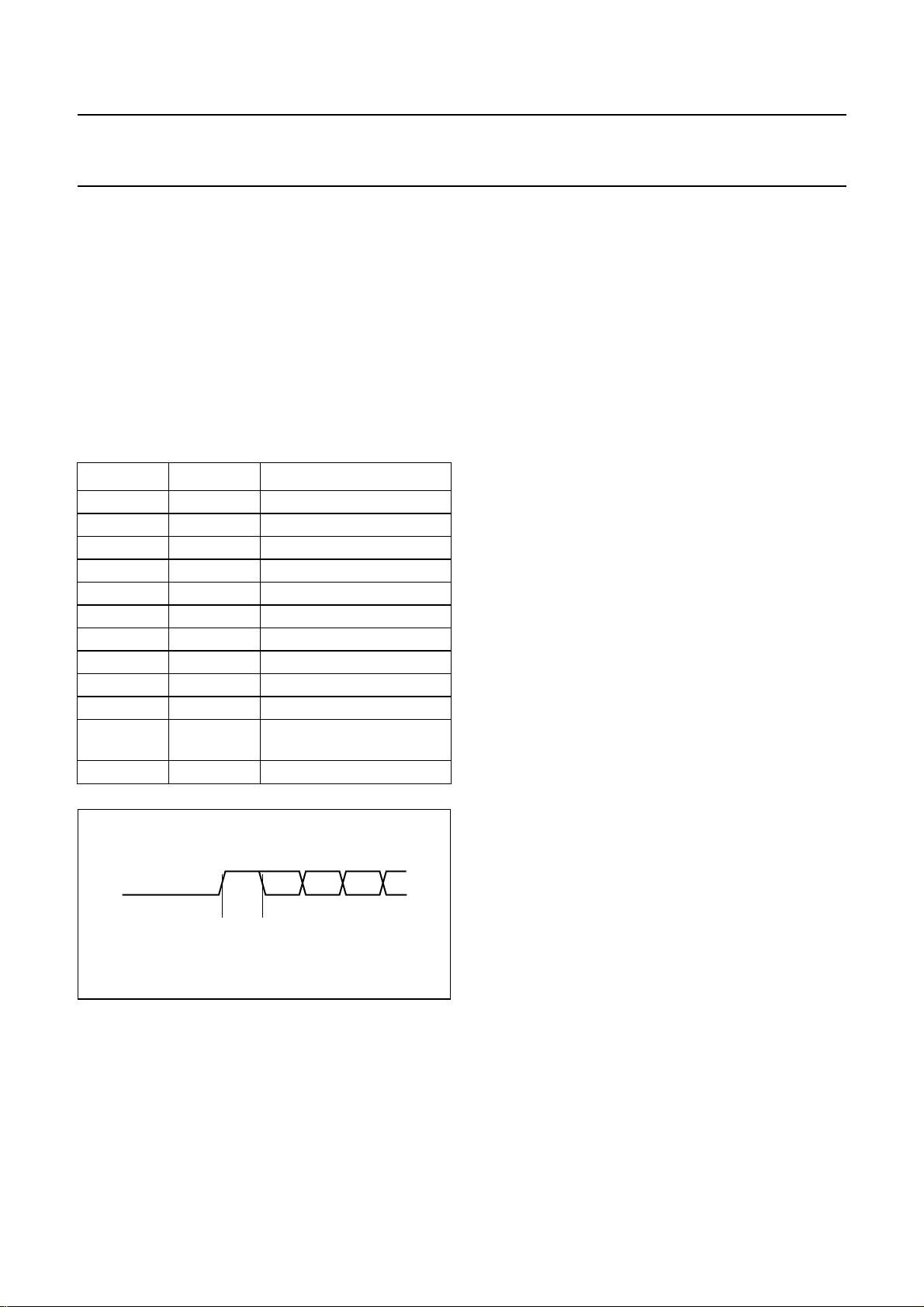
frame consists of 64 bits (each 4 system clock periods
long), beginning with a start bit, then data bits then pause
bits (see Fig.8). The start bit is always preceded by
17 pause bits; and the intermediate start bits at
locations 12, 24 and 36 guarantee that no other ‘1’ bit is
preceded by 17 ‘0’ bits, making the start detection easy.
The structure of the frame is described in Table 23 and
shown in Fig.8.
Table 23 Frame structure
BIT VALUE FUNCTION
0 logic 1 start bit
1 to 10 jitter<9:0> jitter word
11 logic 0
12 logic 1 intermediate start bit
13 to 22 pllfreq<9:0> PLL frequency word
23 logic 0
24 logic 1 intermediate start bit
25 to 32 assym<7:0> asymmetry word
33 logic 0
34 logic 1 intermediate start bit
37 to 46 jitter<9:0> second sample of jitter
word
47 to 63 logic 0 pause
handbook, halfpage
pause data bits
bit 0 bit 1
start
bit
bit 2 bit 3
MGR798
Fig.8 Format on MEAS1 pin.
2000 Mar 21 21
Page 22
Philips Semiconductors Preliminary specification
Channel encoder/decoder CDR60 SAA7392
7.5.3 PLL LOCK SELECT REGISTER (PLLLOCK)
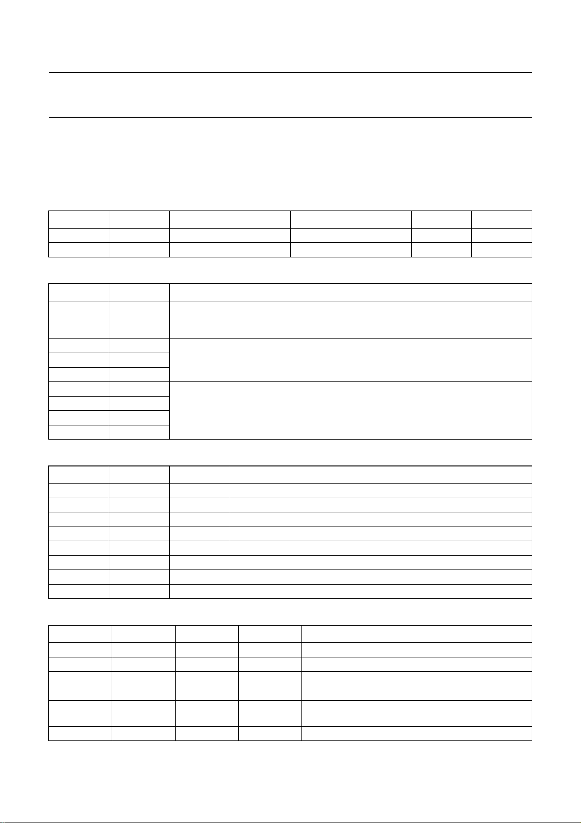
The behaviour of this register is dependent upon whether its being read or written. The behaviour for the write operation
is described in Tables 24 to 27. When read the 8 MSBs of the PLL frequency counter are returned; this is described in
Tables 24 and 28.
Table 24 PLL Lock Select Register (address 00H) - WRITE/READ
76543210
LockOride PhaOset.2 PhaOset.1 PhaOset.0 PLLForceL.3 PLLForceL.2 PLLForceL.1 PLLForceL.0
PLLFreq.7 PLLFreq.6 PLLFreq.5 PLLFreq.4 PLLFreq.3 PLLFreq.2 PLLFreq.1 PLLFreq.0
Table 25 Description of PLLLock bits for write operation
BIT SYMBOL DESCRIPTION
7 LockOride When LockOride = 0, then automatic lock behaviourselected, PLLForceL<3:0>must be
set to ‘0000’. When LockOride = 1, then PLL manual override, PLLForceL<3:0> must
also be programmed.
6 PhaOset.2 These 3 bits are used to select the phase override settings; see Table 26.
5 PhaOset.1
4 PhaOset.0
3 PLLForceL.3 These 4 bits are used to select the PLL lock; see Table 27.
2 PLLForceL.2
1 PLLForceL.1
0 PLLForceL.0
Table 26 Selection of phase override setting
PhaOset.2 PhaOset.1 PhaOset.0 PHASE OVERRIDE
0 0 0 reserved
001
010
011
3
/
×PLL clock over-equalized T3
8
2
/
×PLL clock over-equalized T3
8
1
/
×PLL clock over-equalized T3
8
1 0 0 correct equalisation
101
110
111
1
/
×PLL clock under-equalized T3
8
2
/
×PLL clock under-equalized T3
8
3
/
×PLL clock under-equalized T3
8
Table 27 Selection of PLL lock
PLLForceL.3 PLLForceL.2 PLLForceL.1 PLLForceL.0 PLL LOCK
0000automatic lock behaviour
0001force PLL in-lock
0100force PLL into outer-lock
0110force PLL into inner-lock
1000force PLL into Hold mode (PLL frequency can be
forced using preset value in register PLLFreq)
XXXXall other combinations are reserved
2000 Mar 21 22
Page 23

Philips Semiconductors Preliminary specification
Channel encoder/decoder CDR60 SAA7392
Table 28 Description of PLLock bits for read operation
BIT SYMBOL DESCRIPTION
7 to 0 PLLFreq<7:0> This register holds the 8 MSBs of the PLL frequency counter. The PLL frequency is
calculated as shown below:
f
(Hz)
PLL
7.5.4 PLL B
The function of this register is dependent upon whether its being read or written. The function for the write operation is
described in Tables 29 to 34. Note the measurement conditions are: system clock = 2.15 MHz, bit clock = 4.3 MHz,
bandwidth is proportional to the system clock.
When read this register returns the 8-bit PLL asymmetry value, see Table 29.
Table 29 PLL Bandwidth Select Register (address 01H) - WRITE/READ
76543210
SliceBW.1 SliceBW.0 IntegF0.1 IntegF0.0 PLLBWF1.1 PLLBWF1.0 LPBWF2.1 LPBWF2.0
PLLAsym.7 PLLAsym.6 PLLAsym.5 PLLAsym.4 PLLAsym.3 PLLAsym.2 PLLAsym.1 PLLAsym.0
Table 30 Description of PLLSet bits for write operation
BIT SYMBOL DESCRIPTION
7 SliceBW.1 These 2 bits select the Slicer bandwidth; see Table 31.
6 SliceBW.0
5 IntegF0.1 These 2 bits select the integrator crossover frequency; see Table 32.
4 IntegF0.0
3 PLLBWF1.1 These 2 bits select the PLL bandwidth; see Table 33.
2 PLLBWF1.0
1 LPBWF2.1 These 2 bits select the low-pass bandwidth; see Table 34.
0 LPBWF2.0
ANDWIDTH SELECT REGISTER (PLLSET)
PLLFreq<7:0> ADC clock (Hz)×()
=
-----------------------------------------------------------------------------------------128
Table 31 Selection of Slicer bandwidth
SliceBW.1 SliceBW.0 SLICER BANDWIDTH
0 0 12 Hz
0 1 50 Hz
1 0 200 Hz
1 1 This value is reserved.
Table 32 Selection of integrator crossover frequency
IntegFO.1 IntegFO.0 INTEGRATOR CROSSOVER FREQUENCY
0 0 3780 Hz
0 1 1890 Hz
1 0 945 Hz
1 1 This value is reserved.
2000 Mar 21 23
Page 24
Philips Semiconductors Preliminary specification
Channel encoder/decoder CDR60 SAA7392
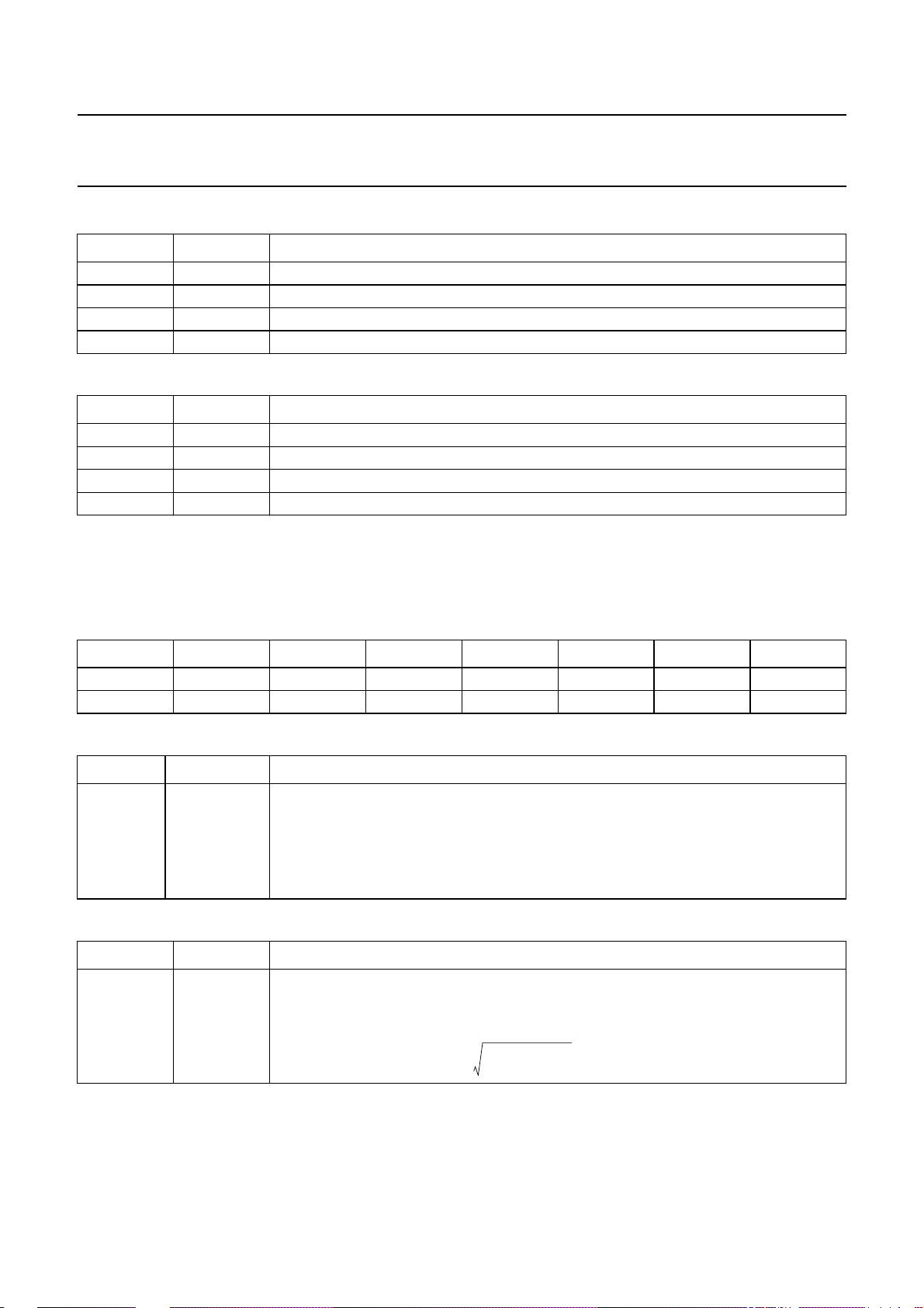
Table 33 Selection of PLL bandwidth
PLLBWF1.1 PLLBWF1.0 PLL BANDWIDTH
0 0 21000 Hz
0 1 10528 Hz
1 0 5264 Hz
1 1 2632 Hz
Table 34 Selection of low-pass bandwidth
LPBWF2.1 LPBWF2.0 LOW-PASS BANDWIDTH
0 0 42100 Hz
0 1 21000 Hz
1 0 10528 Hz
1 1 This value is reserved.
7.5.5 PLL FREQUENCY PRESET REGISTER (PLLFREQ)
The function of this register is dependent upon whether its being read or written. Tables 35 and 36 define the register
function for the write operation. Tables 35 and 37 define the register function for the read operation.
Table 35 PLL Frequency Preset Register (address 02H) - WRITE/READ
76543210
PLLFreq.9 PLLFreq.8 PLLFreq.7 PLLFreq.6 PLLFreq.5 PLLFreq.4 PLLFreq.3 PLLFreq.2
JV.7 JV.6 JV.5 JV.4 JV.3 JV.2 JV.1 JV.0
Table 36 Description of PLLFreq bits for write operation
BIT SYMBOL DESCRIPTION
7 to 0 PLLFreq<9:2> These are the 8 MSBs of the 10-bit code used to set the PLL frequency. The 2 LSBs
reside in the PLLEqu register; these 2 bits should be written to first. The PLL frequency
can be set using the following equation:
f
PLL
PLLFreq<9:0>
--------------------------------------
512
5–
2
+
×=
f
clk
Table 37 Description of PLLFreq bits for read operation
BIT SYMBOL DESCRIPTION
7 to 0 JV.7 to JV.0 Jitter value. These 8 bits determine the PLL clock jitter value (jitter values below 7%
cannot be measuredwith this register). The absoluteclock jitter value can be calculated
as follows:
PLL clock recovery jitter %
2000 Mar 21 24
JV<7:0> 6.5–
------------------------------------ 100×=
2048
Page 25
Philips Semiconductors Preliminary specification
Channel encoder/decoder CDR60 SAA7392
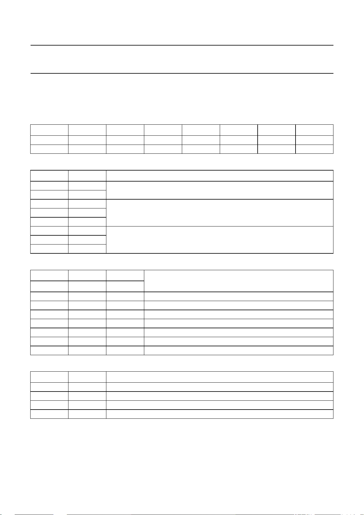
7.5.6 PLL EQUALIZER PRESET REGISTER (PLLEQU)
The functionof thisregister is dependent upon whetherits being read or written.Tables 38, 39and 40 definethe register
function for the write operation. Tables 38 and 41 define the register function for the read operation.
Table 38 PLL Equalizer Preset Register (address 03H) - WRITE/READ
76543210
PLLFreq.1 PLLFreq.0 Tap a1.2 Tapa1.1 Tap a1.0 Tap a2.2 Tap a2.1 Tap a2.0
−−−−−LongSymb FLock InLock
Table 39 Description of PLLEqu bits for write operation
BIT SYMBOL DESCRIPTION
7 PLLFreq.1 These 2 bits are the 2 LSBs of the 10-bit PLL frequency code; see Section 7.5.5.
6 PLLFreq.0
5 Tapa1.2 These 3 bits select the equalizer tap setting a1; see Table 40.
4 Tapa1.1
3 Tapa1.0
2 Tapa2.2 These 3 bits select the equalizer tap setting a2; see Table 40.
1 Tapa2.1
0 Tapa2.0
Table 40 Selection of equalizer tap settings: a1 and a2
Tap a1.2 Tap a1.1 Tap a1.0
Tap a2.2 Tap a2.1 Tap a2.0
0000
001−0.0625
010−0.125
011−0.1875
100−0.25
101−0.3125
X X X All other settings are reserved.
Table 41 Description of PLLEqu bits for read operation
BIT SYMBOL DESCRIPTION
7to3 − These 5 bits are reserved.
2 LongSymb If LongSymb = 1, then a run length of 14 has been detected.
1 FLock If FLock = 1, then PLL is in inner-lock range.
0 InLock If Inlock = 1, then PLL is in lock.
a1 OR a2 EQUALIZER TAP SETTINGS
2000 Mar 21 25
Page 26
Philips Semiconductors Preliminary specification
Channel encoder/decoder CDR60 SAA7392
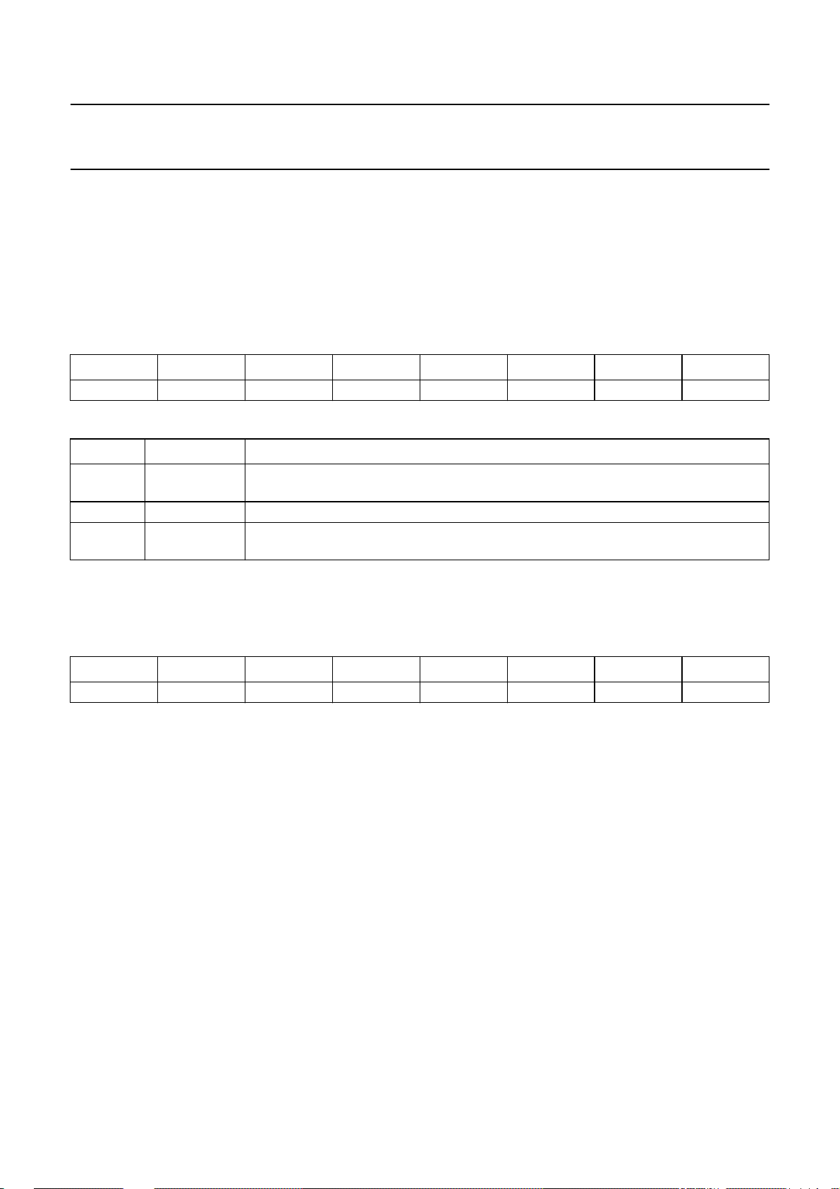
7.5.7 PLL LOCK AID2PRESET REGISTER (PLLFMEAS)
The PLL setting point for the EFM counting locking strategy is controlled by setting the PLL frequency such that, there
are, on average, a fixed number of EFM transitions per PLL clock period:
PLL Locking Frequency/EFM Transition Frequency = (EFM_Count + 32)/16 = 4.75 in a typical application.
Thisvalue (4.75) isdependent ondisc andmechanical variations,improvements maybe achievedby adjusting the value
slightly.
Table 42 PLL Lock Aid2 Preset Register (address 04H) - WRITE
76543210
RL3_En − EFMns.5 EFMns.4 EFMns.3 EFMns.2 EFMns.1 EFMns.0
Table 43 Description of PLLFMeas bits
BIT SYMBOL DESCRIPTION
7 RL3_En If RL3_En = 0, then EFM transition counting outer PLL lock strategy. If RL3_En = 1,
then RL3 detection PLL outer lock strategy.
6 − This bit is reserved.
5 to 0 EFMns<5:0> These 6 bits select the EFM nominal setting. The default nominal setting should be set
to ‘101110’.
7.5.8 MOTOR CONTROL REGISTER 2(MOTOR2)
This is a dual-function register. When read Motor2 gives an indication of the EYE opening of the equalised HF.
Table 44 Eye Open Register (address 0DH) - READ
76543210
EOV.7 EOV.6 EOV.5 EOV.4 EOV.3 EOV.2 EOV.1 EOV.0
2000 Mar 21 26
Page 27
Philips Semiconductors Preliminary specification
Channel encoder/decoder CDR60 SAA7392
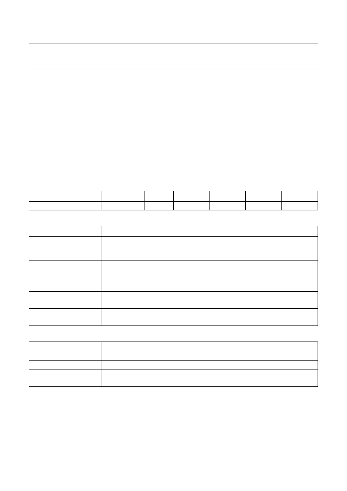
7.5.9 VITERBI DETECTOR SETTING REGISTER (VITSET)
Thisregister controlsanadvanced dataslicerfor improved
bit detector performance.
• An adaptive slicer performs a second slice operation.
This has a higher bandwidth than the first slicer.
• Ifswitched on,the runlength 2push-back circuitpushes
allrun lengthtwo symbolsto run length 3.The circuitwill
determine which transition was most likely in error and
shift transition on that edge.
To avoid advanced detector hang-up, caused by a
detection level that is too high and is not brought down, a
Watchdog counter on the slicer level is installed.
Table 45 Viterbi Detector Setting Register (address 16H) - WRITE
76 543210
AdSliceON AdDetON FEndAutoSON RL2PB WDog MaxCnt WDogCnt.1 WDogCnt.0
Table 46 Description of VitSet bits
BIT SYMBOL DESCRIPTION
7 AdSliceON If AdSliceON = 0, then slicer reset (to logic 0). If AdSliceON = 1, then slicer active.
6 AdDetON If AdDetON = 0, then advanced bit detector off. If AdDetON = 1, then advanced bit
detector on.
5 FEndAutoSON If FEndAutoSON = 0, then auto-scaling in front-end Hold mode. If FEndAutoSON = 1,
then auto-scaling in front-end on.
4 RL2PB If RL2PB = 0, then run length 2 push-back off. If RL2PB = 1, then run length 2
push-back on.
3 WDog If WDog = 0, then slicer Watchdog is off. If WDog = 1, then slicer Watchdog is on.
2 MaxCnt If MaxCnt = 0, then maxcount is 1024. If MaxCnt = 1, then maxcount is 2048.
1 WDogCnt.1 These 2 bits select the Watchdog count step; see Table 47.
0 WDogCnt.0
The Watchdog counter is a counter that counts on the
front-end PLL clock.
• If rl1 or a rl2 received: count + stepsize
• Elsif no transition: count + 1
• Elsif transition on a valid runlength: count − 8
• Elsif (count > maxcount): reset count.
Stepsize and maxcountcan be set by writing to the VitSet
register. On a reset of the counter the slice level is also
reset.
Table 47 Selection of Watchdog count step
WDogCnt.1 WDogCnt.0 WATCHDOG COUNT STEP
00 32
01 64
1 0 128
1 1 256
7.5.10 M
When read this register holds the 8-bit advanced slicer compensation value.
2000 Mar 21 27
OTOR CONTROL REGISTER 1(MOTOR1)
Page 28
Philips Semiconductors Preliminary specification
Channel encoder/decoder CDR60 SAA7392
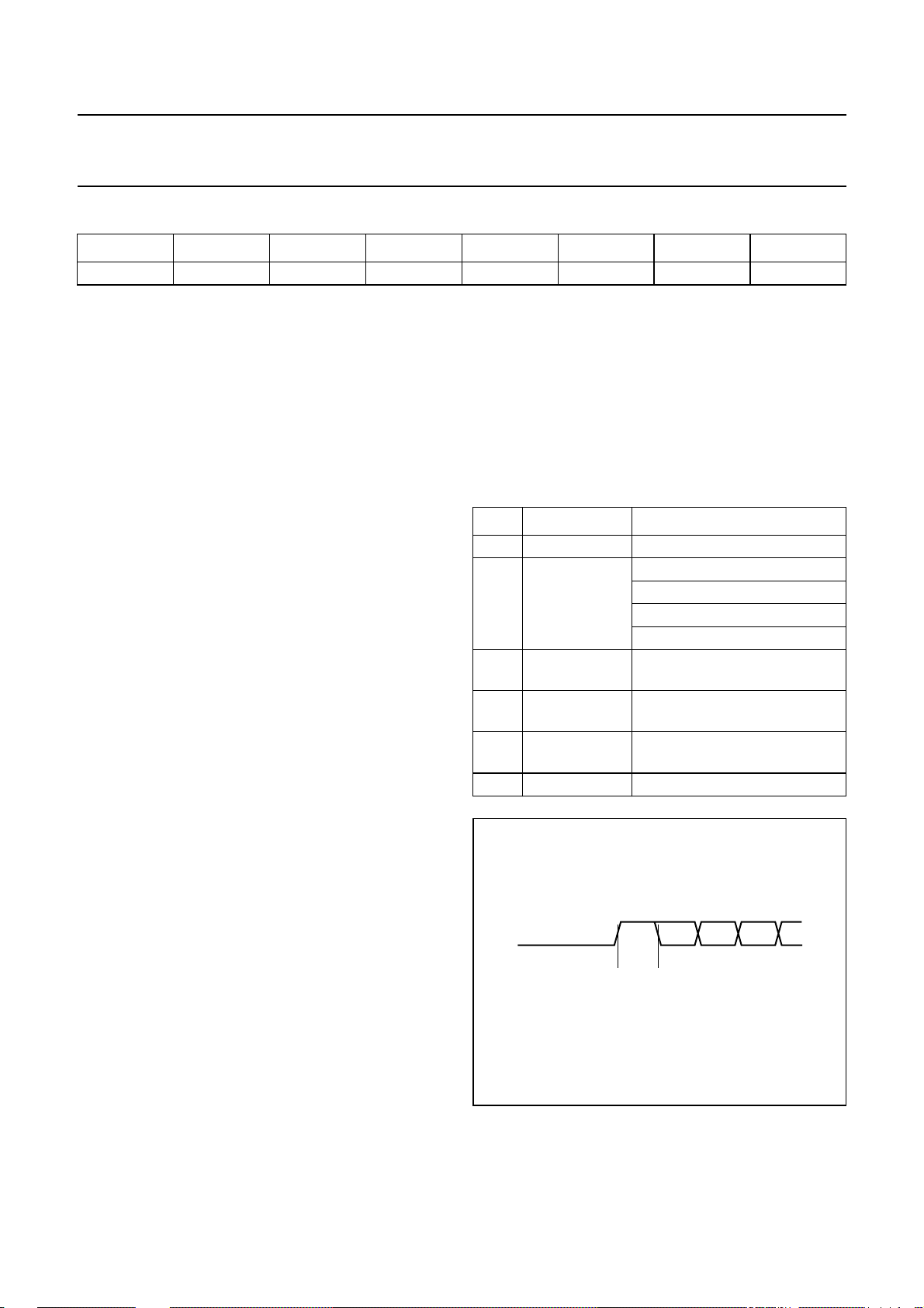
Table 48 Motor Control Register 1 (address 0CH) - READ
76543210
ASCV.7 ASCV.6 ASCV.5 ASCV.4 ASCV.3 ASCV.2 ASCV.1 ASCV.0
7.6 Decoder function
7.6.1 DEMODULATOR
The demodulator block includes sync extraction,
interpolation and protection circuits, and converts the
14-bit EFM data and subcode words into 8-bit symbols.
Two counters are used to detect frame synchronisation.
The coincidence counter detects the coincidence of
successive syncs (i.e. 2 syncs are within
588 ± 1 EFM clock). The main counter partitions the EFM
signal into 16 or 17-bit bytes; and is reset when a sync
coincidence is found or the sync pulse is within ±6 EFM
clock pulses. The sync coincidence signal generates the
‘lock’ signal which goes active HIGH when one sync
coincidence is found, and goes inactive when no sync
coincidence is found within 61 consecutive EFM frames.
The frame sync detection circuit extracts the frame sync
and will guard against mis-detection; up to 7 consecutive
corrupted syncs will not disturb the sync detection.
After data demodulation the sector sync is extracted; a
doublelock counteris used.The maincounter interpolates
the sector syncs, and a coincidence counter resets the
main counter.
7.6.2 ERROR CORRECTOR
The error corrector can correct up to 2 errors on the
C1 level and up to 4 errors on the C2 level. The error
corrector also contains a flag processor. Flags are
assigned to symbols when the error corrector cannot
ascertain if the symbols are definitely good.C1 generates
output flags that are used by C2. The C2 output flags are
output via the FLAG signal along with the I2S, and can be
used by the interpolator for concealment of uncorrectable
errors for audio output.
• Muting of data. Data output via the serial interface
and/or the EBU can be set to zero using register
Output3.
• Concealment of audio errors. A simple 1 sample
linear interpolator can be selected via register Output3.
If selected the interpolator becomes active if a single
sample is flagged as erroneous; left and right channels
have independent interpolators.
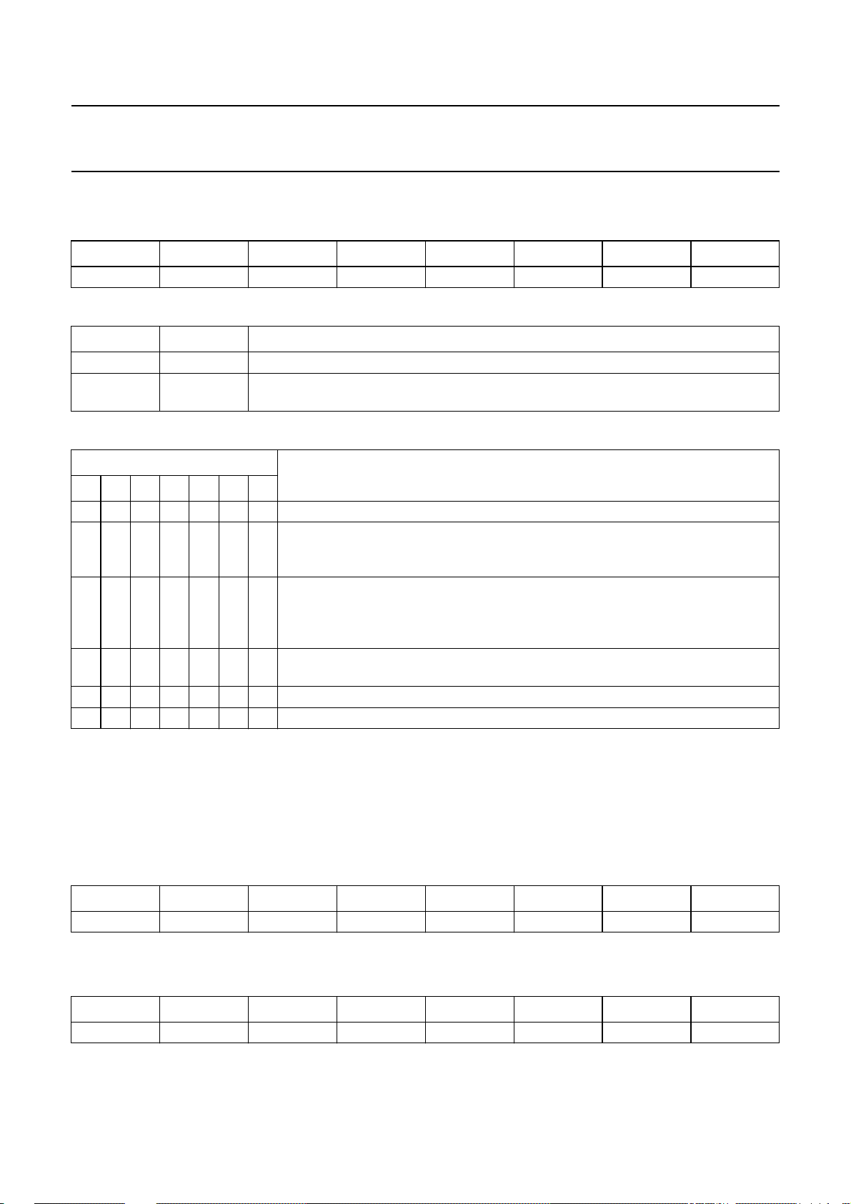
7.6.2.1 CFLG pin
The error corrector outputs status information in serial
format on the CFLG pin. Each frame consists of 11 bits
(each 7 system clock periods long), beginning with a start
bit, then data bits then pause bit (see Fig.9). The repetition
rate of CFLGis notfixed; itdepends onthe discspeed and
output interface speed. There is always at least one pause
bit. The structure of the frame is shown in Table 49.
Table 49 Frame structure
BIT VALUE COMMENT
0 logic 1 start bit
1 to 3 cormode<2:0> 000 = C1 correction
011 = C2 correction
100 = corrector not active
all other codes not used
4 corfail failure flag set because
correction impossible
5 flagfail failure flag set because
correction too risky
6 to 9 rootcount<3:0> number of errors corrected,
after Euclidean algorithm
10 logic 0 pause bit
handbook, halfpage
pause data bits
bit 0 bit 1
start
bit
bit 2 bit 3
MGR798
Fig.9 Format on CFLG pin.
2000 Mar 21 28
Page 29
Philips Semiconductors Preliminary specification
Channel encoder/decoder CDR60 SAA7392
7.6.3 DECODER MODE SELECT REGISTER (DECOMODE)
Table 50 Decoder Mode Select Register (address 13H) - WRITE
76543210
Mode.6 Mode.5 Mode.4 Mode.3 Mode.2 Mode.1 Mode.0 LWCon
Table 51 Description of DecoMode bits
BIT SYMBOL DESCRIPTION
7 to 1 Mode<6:0> These 7 bits select the Decoder mode; see Table 52.
0 LWCon When a logic 0, LaserOn and WriteOn2 signals operate normally. When a logic 1,
LaserOn and WriteOn2 signals are reset.
Table 52 Selection of Decoder mode
MODE
6543210
0000000Flush mode. Deinterleaver table is emptied and all data is discarded.
0100000Normal play. Uses the Quad-pass error correction mode used for disc speeds up
to 75% of maximum defined by ADCCLK. Note the data integrity should be
checked using the CRC as the FLAG pin is not fully defined in this mode.
0101000Fast play. Used for audio play or fast CDROM mode (25 to 100% of maximum
defined by ADCCLK), this reduces the error correction performance, but also
halves the throughput time of error corrector (only dual pass error correction
algorithm used).
0110000Hold mode. Data into output FIFO is stopped (header/subheader decoding
remains operative).
0101010Encode mode.
X X X X X X X All other combinations reserved.
7.6.4 F
These two registers are non-buffered counters. Each time a C1 frame with errors is found the register C1BLER is
incremented. In the same way C2BLER increments on all C2 frames with errors. When the value of either register
reaches 255, it will hold. When read, the register value is reset.
RAME ERROR STATUS REGISTERS (C1BLER AND C2BLER)
DECODER MODE
7.6.4.1 C1 Block Error Register (C1BLER)
Table 53 C1 Block Error Register (address 39H) - READ
76543210
C1BLER.7 C1BLER.6 C1BLER.5 C1BLER.4 C1BLER.3 C1BLER.2 C1BLER.1 C1BLER.0
7.6.4.2 C2 Block Error Register (C2BLER)
Table 54 C2 Block Error Register (address 3AH) - READ
76543210
C2BLER.7 C2BLER.6 C2BLER.5 C2BLER.4 C2BLER.3 C2BLER.2 C2BLER.1 C2BLER.0
2000 Mar 21 29
Page 30

Philips Semiconductors Preliminary specification
Channel encoder/decoder CDR60 SAA7392
7.6.5 DATA FIFO
Thedecoder blockcan beviewed as aFIFO, demodulated
data is written in while the output interface reads from it.
The way in which the FIFO is filled depends on the
decoder mode set via register DecoMode. The decoder
modes that effect the filling of the FIFO are described in
Sections 7.6.5.1 to 7.6.5.3.
Data is read out via the output interface and is only
possible if enough data is present in the FIFO. The
minimumamount ofdata is110 C1 frames (C1 frame = 24
user bytes).
7.6.5.1 Flush mode
The FIFO contentis thrown away; no read-out possible. It
is necessary to flush the FIFO every time a context switch
is made; when data written to the FIFO is not subsequent
with data already present in the FIFO.
7.6.5.2 Hold mode
Writing to the FIFO is stopped; read-out possible if FIFO
wasfilled. Thismodeis intendedtoavoid FIFOoverflowby
implementing a ‘stop write - jump back’ action in the
microprocessor. When the microprocessor switches to
hold mode the switch-over is synchronised internally with
the next subcode block start, allowing the microprocessor
to know exactly where the writing will stop or start. This
mode is also intended to avoid overflow in the block
decoder; on imminent overflow the microprocessor can
switch to hold mode. When it jumps back one track and
switches off hold mode on the samesubcode address the
SAA7392 will make a seamless link.
7.6.5.3 Play mode
7.6.5.4 Data FIFO monitoring
The state of the internal data FIFO may be monitored by
reading the AnaSet1 register. This gives the number of
C1 frames present in the FIFO including those frames in
the outer corrector (i.e. 110 in CD fast and 220 in
CD normal). One C1 frame equates to 24 user bytes in
CD mode).
7.7 Subcode interface
Q-channel subcode data can be read using the ClockPre
and DecoMode registers. The ClockPre register must be
read first; this contains the status of the Q-channel
subcode that maybe read. Reading the ClockPreregister
with Ready = 1 will block the subcode interface for data
read; no new subcode will overwrite the current subcode,
and the microprocessor may retrieve as many bytes (up
to 12) as required by issuing reads to register DecoMode.
After finishing the subcode read the microprocessor must
release the interface by issuing a read to the dummy
register SubReadEnd (no data can be read from it); this
allows the SAA7392 to capture new subcode frames.
The serial Q to W subcode is output on the V4 pin as
illustrated in Fig.10. The subcode sync word is formed by
a pause of
200
/nµs minimum; where n = the disc speed.
Each subcode word starts with a logic 1followed by 7 bits
(Q to W); the bit time is 0.5 of the period of the WCLK
signal, (
11.3
11.3
/nµs). The gap between the words is between
/n and90/nµs. Note that the subcode data cannot be
guaranteed at a rate higher than 0.5 × the maximum data
rate programmed.
The subcode data is also available in the EBU output
(EBUOUT).
The FIFO is filled; read-out possible when FIFO filling big
enough.
handbook, full pagewidth
n = disc speed
200/n µs min 11.3/n µs
W96
1 Q1 R1 S1 T U1 V W1 1 Q2
Fig.10 Subcode format and timing on V4 pin.
2000 Mar 21 30
11.3/n µs min
90/n µs max
MGR799
Page 31
Philips Semiconductors Preliminary specification
Channel encoder/decoder CDR60 SAA7392
7.7.1 CLOCK PRESET REGISTER (CLOCKPRE)
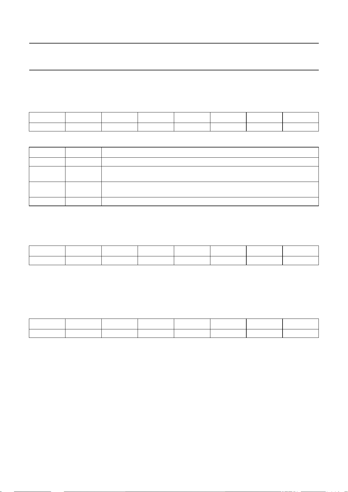
This is a dual-function register. When read the status of the Q-channel is returned.
Table 55 Clock Preset Register (address 12H) - READ
76543210
Ready Busy CRC OK −−−−−
Table 56 Description of ClockPre bits
BIT SYMBOL DESCRIPTION
7 Ready If Ready = 0, then buffer filling. If Ready = 1, then valid Q subcode frame available.
6 Busy If Busy = 0, then buffer filling. If Busy = 1, then buffer held (set after reading this register
with Ready = 1).
5 CRC OK If CRC OK = 0, then CRC not checked or not OK. If CRC OK = 1, then CRC of
Q-channel checks OK, only valid if Ready = 1.
4to0 − These 5 bits are reserved.
7.7.2 D
This is a dual-function register. When read this register holds the Q-channel subcode data.
Table 57 Decoder Mode Select Register (address 13H) - READ
7.7.3 S
After finishing a subcode read, the microprocessor must release the interface to allow the SAA7392 to capture new
subcode frames. This is done by issuing a read to SubReadEnd. No data can be read from this register; only the side
effect is important.
Table 58 Subcode Read End Register (address 14H) - READ
ECODER MODE SELECT REGISTER (DECOMODE)
76543210
SubD.7 SubD.6 SubD.5 SubD.4 SubD.3 SubD.2 SubD.1 SubD.0
UBCODE READ END REGISTER (SUBREADEND)
76543210
−−−−−−−−
2000 Mar 21 31
Page 32
Philips Semiconductors Preliminary specification
Channel encoder/decoder CDR60 SAA7392
7.8 Digital output
The AES/EBU signal is available on pin EBUOUT,
according to the format defined by the
specification”
. This signal is only available in the CLV
“IEC958
modes of the decoder (not in QCLV). Three different
modes can be selected:
• EBU off
The EBU interface uses a clock derived from XTLI for
timing generation. For correct operation of the EBU
interface, BCLKmust be non-gated and the selected EBU
clock and BCLK must fulfil the following constraint:
EBU clock WCLK 64×=
WCLK is BCLK divided by 16, 24 or 32 depending on the
chosen output format.
• EBU data all zero
• EBU data valid.
7.8.1 INPUT CONFIGURATION REGISTER (INPUTCONFIG)
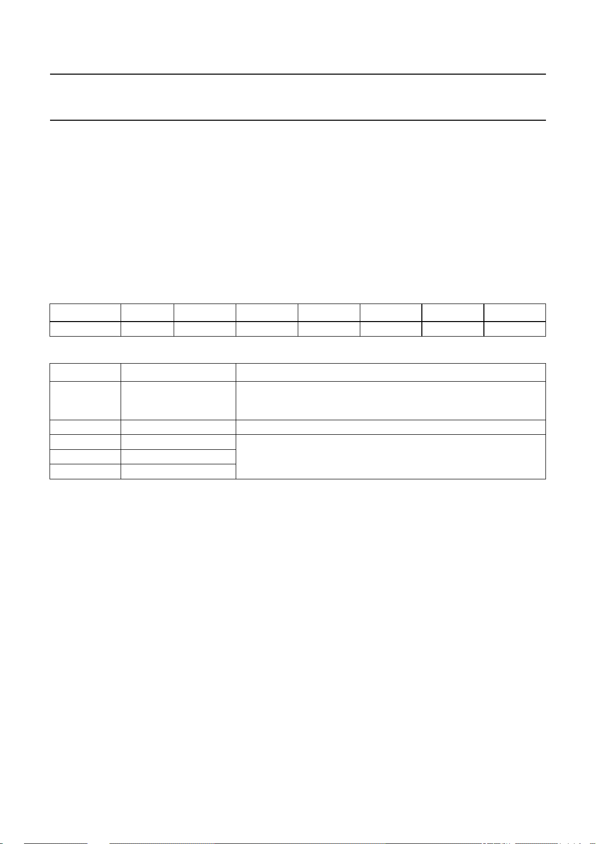
Table 59 Input Configuration Register (address 1EH) - WRITE
76543210
EBUClkSelect −−−−ScramOn InputFmt.1 InputFmt.0
Table 60 Description of InputConfig bits
BIT SYMBOL DESCRIPTION
1
/3f
XTLI
XTLI
(input
. If
7 EBUClkSelect If EBUClkSelect = 0, then the EBU clock frequency is
EBUClkSelect = 1, then the EBU clock frequency is2/3f
MUXSWI must be a logic 1 for this setting).
6to3 − These 4 bits are reserved.
2 ScramOn See Section 7.11.1.
1 InputFmt1
0 InputFmt0
2000 Mar 21 32
Page 33

Philips Semiconductors Preliminary specification
Channel encoder/decoder CDR60 SAA7392
7.8.2 FORMAT
The digital audio output consists of 32-bit words (subframes) transmitted in biphasemark code (two transitions for a
logic 1 and one transition for a logic 0). Words are transmitted in blocks of 384.
Table 61 Digital audio output subframe format
BIT FIELD NAME DESCRIPTION
0 to 3 sync The sync word is formed by violation of the biphase rule and therefore does not
contain any data. Its length is equivalent to 4 data bits. The 3 different sync patterns
indicate the following situations:
• Sync B: Start of a block (384 words), word contains left sample
• Sync M: Word contains left sample (no block start)
• Sync W: Word contains right sample.
4 to 7 auxiliary These bits are not used; normally zero.
8 to 27 audio sample Left and right samples are transmitted alternately. The first 4 bits not used (always
zero); 2’s compliment; LSB = bit 12 and MSB = bit 27.
28 validity flag If validity flag = 1, audio samples are flagged if an error has been detected but was
uncorrectable. This flag remains the same even if data is taken after concealment.
29 user data Subcode bits Q until W from the subcode section are transmitted via the user data
bit. This data is asynchronous with the block rate.
30 channel status The channel status bit is the same for left and right words. Therefore, a block of
384 words contains 192 channel status bits. The category code is always CD. The bit
assignment is shown in Table 62.
31 parity bit Even parity for bits 4 to 30.
Table 62 Channel status bit assignment
BIT FIELD NAME DESCRIPTION
0 to 4 control Bits 1 to 4 copied from register Output2. Bit 2 is logic 1 when copy permitted. Bit 3 is
logic 1 when recording has pre-emphasis
5 to 7 reserved mode always zero
8 to 15 category code CD: bit 8 = logic 1, all other bits = logic 0
28 to 29 clock accuracy set by register Output2:
10 = level I
00 = level II
01 = level III
16 to 27, remaining always zero
30 to 191
2000 Mar 21 33
Page 34
Philips Semiconductors Preliminary specification
Channel encoder/decoder CDR60 SAA7392
7.9 Serial output interface
The serial data output interface consists of three signals:
WCLK (word select), BCLK (serial clock), DATAO (serial
data). The polarity of WCLK and the data can be inverted.
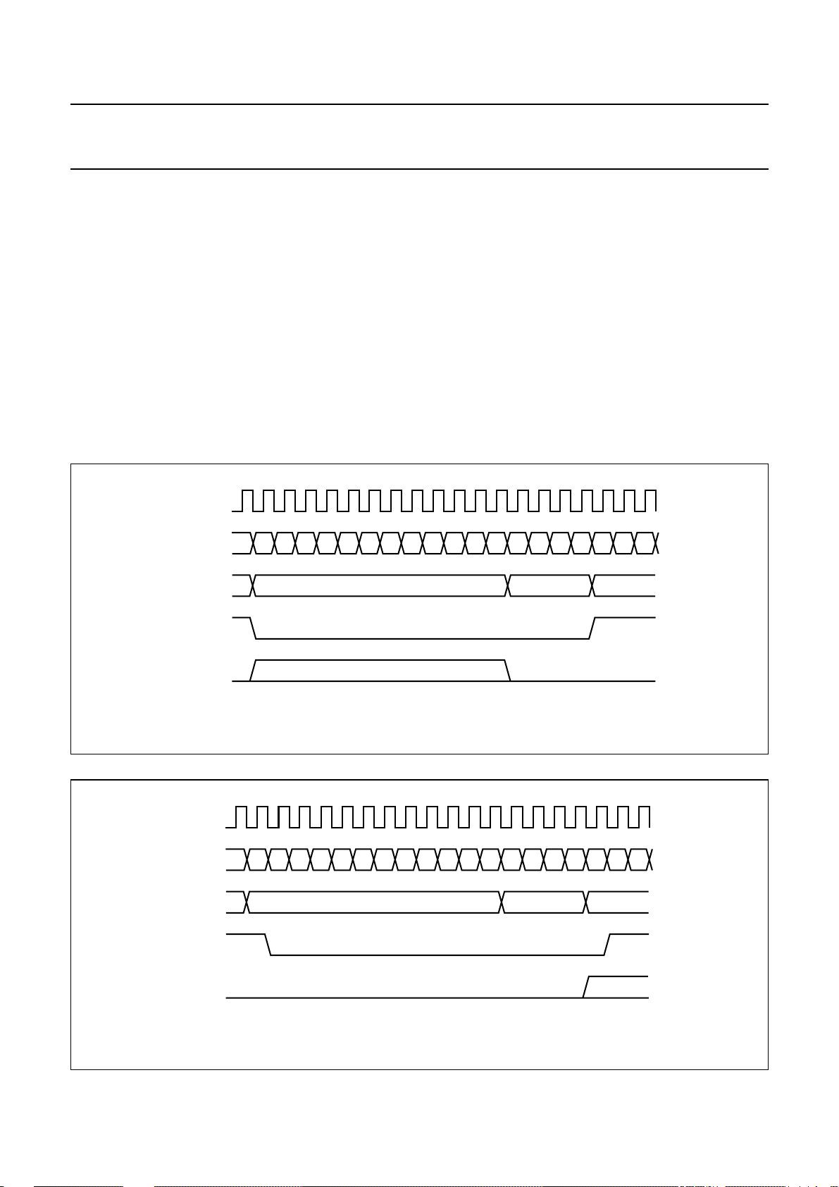
The FLAG signal is used to identify if there are errors in
either the LSB or MSB of the 16-bit data word. The
interfacecan beused asamaster orslaveinterface (BCLK
and WCLK are then inputs), selectable by register
Output1.
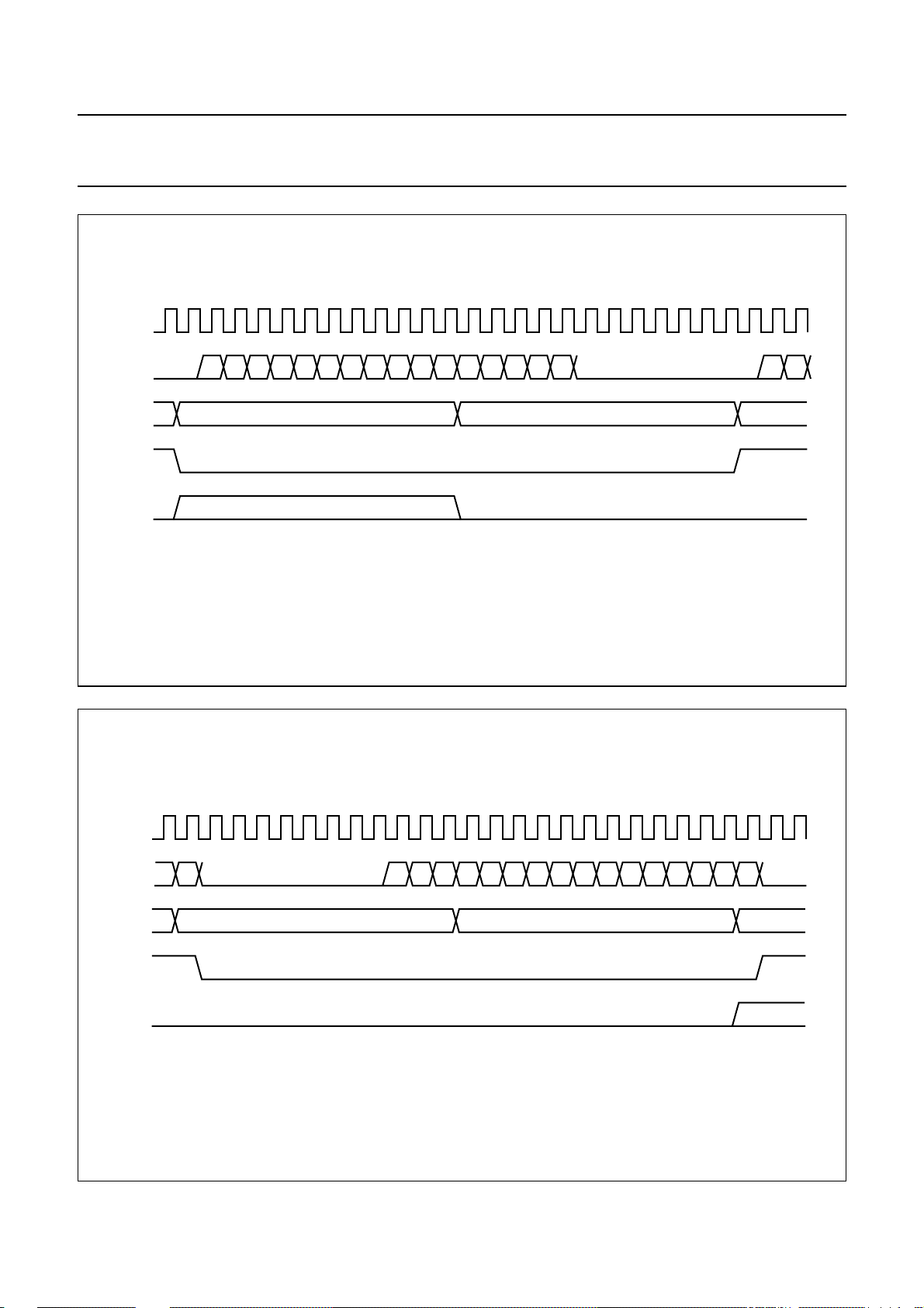
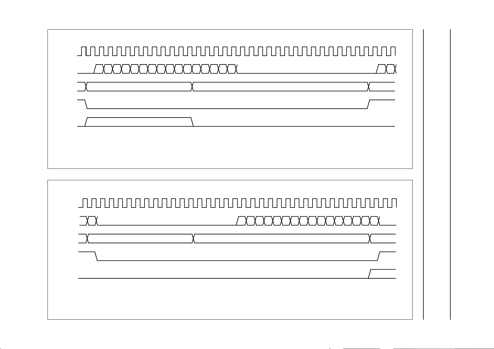
The serial datainterface can be switched into two modes:
PhilipsI2Sand theEIAJformat (theprotocol can useeither
16, 24 or 32 BCLK clocks for each 16-bit output,
selectable by Output1register). The formats are shownin
Figs 11 to 16.
handbook, full pagewidth
BCLK
D15
DATA
FLAG FLAG - MSB (1 is unreliable) FLAG - LSB
D14 D13 D12 D11 D10 D9 D8 D7 D6 D5 D4 D3 D2 D1 D0D1 D0 D15 D14
The BCLK frequency can be selected by register
ClockPre, or input externally. If the data out rate does not
correspond with the disc speed and the bit clock data, the
FIFO will either fill or empty. FIFO underflow (STOPCK
output goes HIGH indicating absence of data) must be
avoided. If BCLK is an input, it should be stopped and
restarted again when STOPCK goes LOW. If BCLK is
output, it is automatically stopped if BCLK gate enable is
set(via registerClockPre);if itisnot setthenunpredictable
operation will result.
handbook, full pagewidth
WCLK
SYNC
left
Fig.11 Format 1: 16 clocks/word I2S format.
BCLK
D15
DATA
FLAG FLAG - MSB (1 is unreliable) FLAG - LSB
WCLK
SYNC
D14 D13 D12 D11 D10 D9 D8 D7 D6 D5 D4 D3 D2 D1 D0D1 D0 D15 D14
right
right
MGR800
left
MGR801
Fig.12 Format 2: 16 clocks/word ‘S’ format (WCLK inverted).
2000 Mar 21 34
Page 35
Philips Semiconductors Preliminary specification
Channel encoder/decoder CDR60 SAA7392
handbook, full pagewidth
BCLK
D15
DATA
FLAG FLAG - MSB (1 is unreliable) FLAG - LSB
D14 D13 D12 D11 D10 D9 D8 D7 D6 D5 D4 D3 D2 D1 D0 D15 D14
WCLK
SYNC
handbook, full pagewidth
BCLK
DATA
left
Fig.13 Format 3: 24 clocks/word I2S format.
D15
D14 D13 D12 D11 D10 D9 D8 D7 D6 D5 D4 D3 D2 D1 D0D1 D0
right
MGR802
FLAG FLAG - MSB (1 is unreliable) FLAG - LSB
WCLK
SYNC
right
Fig.14 Format 4: 24 clocks/word ‘S’ format (WCLK inverted).
2000 Mar 21 35
left
MGR803
Page 36
This text is here in white to force landscape pages to be rotated correctly when browsing through the pdf in the Acrobat reader.This text is here in
_white to force landscape pages to be rotated correctly when browsing through the pdf in the Acrobat reader.This text is here inThis text is here in
white to force landscape pages to be rotated correctly when browsingthrough the pdf inthe Acrobat reader. white to force landscape pages to be ...
2000 Mar 21 36
BCLK
D15
DATA
FLAG FLAG - MSB (1 is unreliable) FLAG - LSB
D14 D13 D12 D11 D10 D9 D8 D7 D6 D5 D4 D3 D2 D1 D0 D15 D14
Philips Semiconductors Preliminary specification
Channel encoder/decoder CDR60 SAA7392
WCLK
SYNC
left
Fig.15 Format 5: 32 clocks/word I2S format.
BCLK
D15
DATA
FLAG FLAG - MSB (1 is unreliable) FLAG - LSB
WCLK
right
D14 D13 D12 D11 D10 D9 D8 D7 D6 D5 D4 D3 D2 D1 D0D1 D0
right
MGR804
left
SYNC
MGR805
Fig.16 Format 6: 32 clocks/word ‘S’ format (WCLK inverted).
Page 37
Philips Semiconductors Preliminary specification
Channel encoder/decoder CDR60 SAA7392
7.9.1 I2SOUTPUT REGISTER (OUTPUT1)
2
Table 63 I
Format.2 Format.1 Format.0 WClkIO BClkIO −−−
Table 64 Description of Output1 bits
S Output Register 1 (address 05H) - WRITE
76543210
BIT SYMBOL DESCRIPTION
7 Format.2 These 3 bits select the format; see Table 65.
6 Format.1
5 Format.0
4 WClkIO When WClkIO = 0, then WCLK is in Input mode. When WClkIO = 1, then WCLK is in
Output mode.
3 BClkIO When BClkIO = 0, then BCLK is in Input mode. When BClkIO = 1, then BCLK is in
Output mode.
2to0 − These 3 bits are reserved.
Table 65 Format selection
Format.2 Format.1 Format.0 FORMAT
0 0 0 Format 1
0 0 1 Format 2
0 1 0 Format 3
0 1 1 Format 4
1 0 0 Format 5
1 0 1 Format 6
7.9.2 I
Table 66 I
2
SOUTPUT REGISTER 2(OUTPUT2)
2
S Output Register 2 (address 06H) - WRITE
76543210
EBUValid EBUOn EBUCon.29 EBUCon.28 EBUCon.3 EBUCon.2 EBUCon.1 EBUCon.0
Table 67 Description of Output2 bits
BIT SYMBOL DESCRIPTION
7 EBUValid If EBUValid= 0, then EBU/IEC958 output data zero. If EBUValid = 1, then EBU/IEC958
output data valid.
6 EBUOn If EBUOn = 0, then EBU/IEC958 outputis switched off. If EBUOn =1, then EBU/IEC958
output switched on.
5 EBUCon.29 These 2 bits are copied to bits 29 and 28 of the IEC958 control channel (crystal
4 EBUCon.28
accuracy); see Table 62.
3 to 0 EBUCon<3:0> These 4 bits are copied to bits 4 to 1 of the IEC958 control channel (data/audio, copy
protect, de-emphasis); see Table 62.
2000 Mar 21 37
Page 38

Philips Semiconductors Preliminary specification
Channel encoder/decoder CDR60 SAA7392
7.9.3 I2SOUTPUT REGISTER 3(OUTPUT3)
2
Table 68 I
WClkHLeft DescrmOn InterpOn − FlagPin KillDataOn KillEBUOn −
Table 69 Description of Output3 bits
S Output Register 3 (address 07H) - WRITE
76543210
BIT SYMBOL DESCRIPTION
7 WClkHLeft When WClkHLeft = 0, then WCLK is HIGH on right byte of I2S/S format output; (use for
I2S format modes). When WCLKHLeft = 1, then WCLK is HIGH on left byte of I2S/S
format output; (use for S format modes).
6 DescrmOn When DescrmOn = 1, then Descrambling function on.
For CD-DA playbackdescrambling has tobe switched off.For CD-ROMdescrambling is
required but it might also be possible that a descrambling function is available in the
buffer manager (block decoder).
5 InterpOn When InterpOn = 0, then audio data interpolation is switched off. When InterpOn = 1,
then audio data interpolation switched on.
4 − This bit is reserved.
3 FlagPin When FlagPin = 0, then flag pin sends out EDC-OK signal on byte 2063 of the sector.
When FlagPin = 1, then flag pin sends out reliability flag information.
2 KillDataOn When KillDataOn = 0, then in normal mode. When KillDataOn = 1, then all data inserial
output channel is set to zero.
1 KillEBUOn When KillEBUOn = 0, then in normal mode. When KillEBUOn = 1, then all data in
IEC958/EBU channel is set to zero
0 − This bit is reserved.
2000 Mar 21 38
Page 39
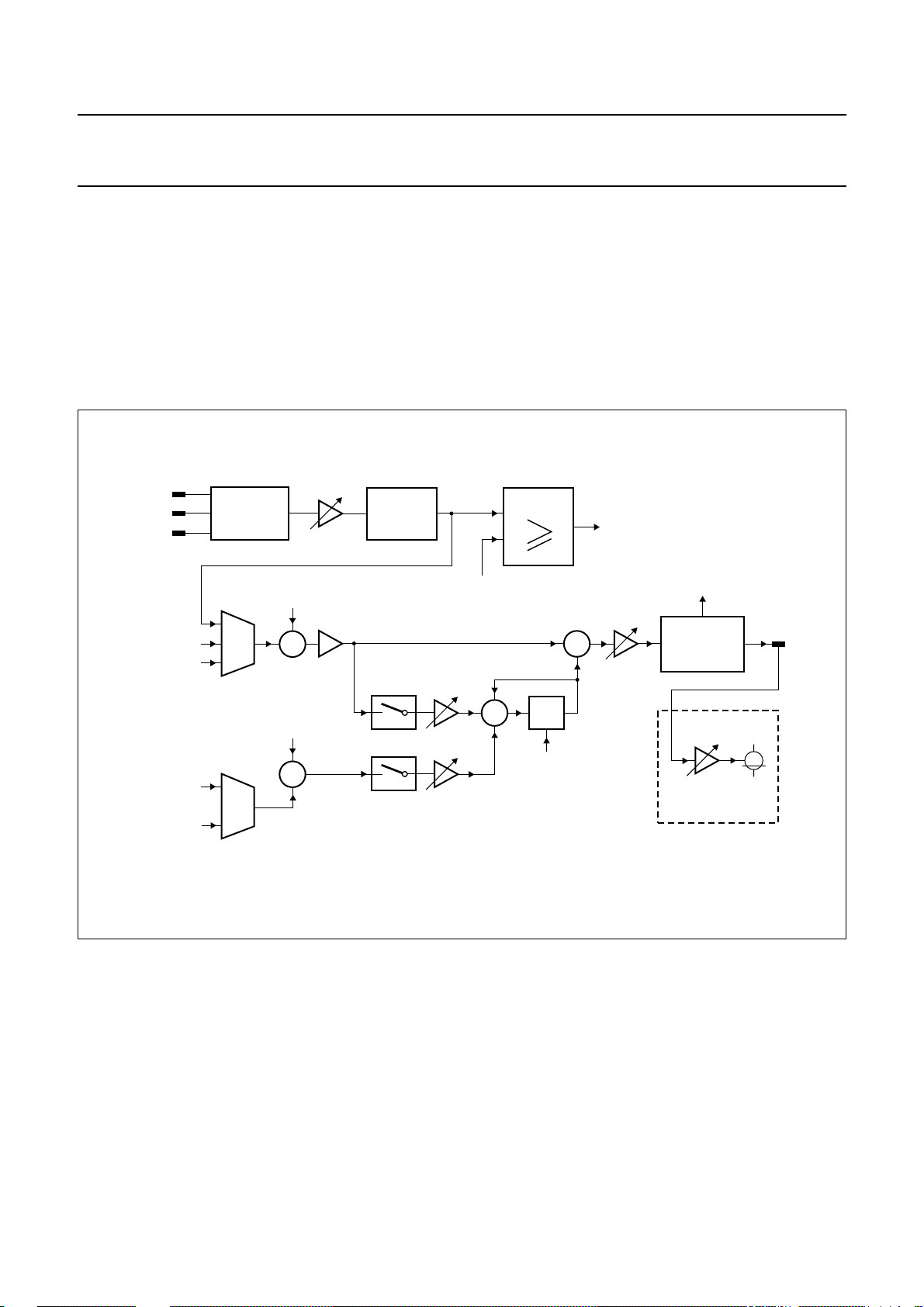
Philips Semiconductors Preliminary specification
Channel encoder/decoder CDR60 SAA7392
7.10 Motor control
The spindle motor is controlled by a fully integrated digital servo sub-system within the SAA7392. Information from the
data FIFO, data recovery PLL and tacho inputs may be used to calculate the motor control output signals.
The frequency set-point, the FIFO settings and coefficients G, Kiand Kf are all programmable using the seven motor
control registers. The motor can be controlled in either Pulse Width Mode (PWM) or Pulse Density Mode (PDM).
The tacho controlsubsystem allows a range ofdifferent motor tacho systems to be used, the modes and prescalers are
programmable via the tacho register set. (Note due to pin multiplexing, PWM motor control mode and CAV mode using
tacho control are mutually exclusive).
handbook, full pagewidth
T1
T2
MOTO2/T3
Wobble frequency
PLL frequency
FIFO filling
XError
TRANSITION
DETECTOR
frequency/tacho
set-point
+
FIFO half-full
−
+
set-point
−
+
+
tacho
TACHO
LOW-PASS
K
tacho
1/(2.667 × system clock)
FILTER
SW1
frequency
tacho
set-point
+
K
SW2
Fig.17 Motor servo block diagram.
i
K
f
COMPARE
24T
reset
tacho
interrupt
overflow
detector
M
MGR807
motor
pads
+
G
PDM/PWM
MODULATOR
analog output
stage gain
G
E
EXTERNAL
MOTOR CIRCUIT
motor
2000 Mar 21 39
Page 40
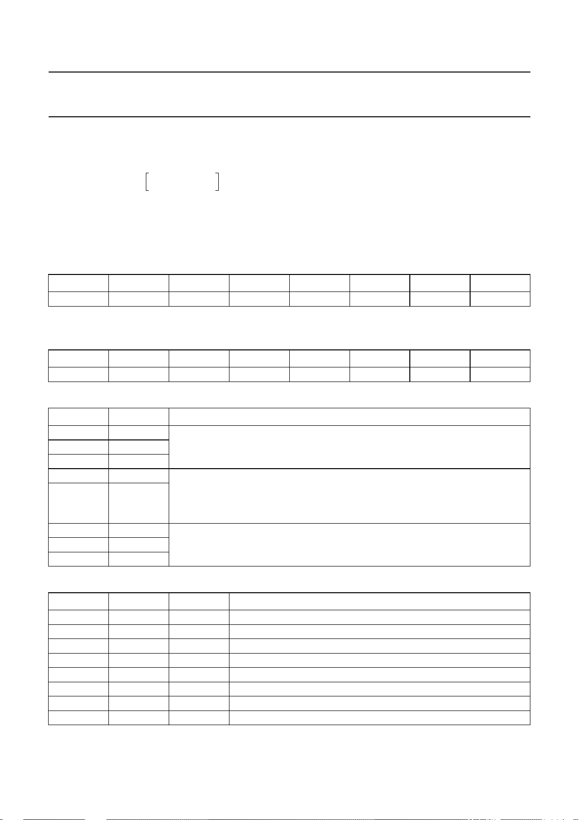
Philips Semiconductors Preliminary specification
Channel encoder/decoder CDR60 SAA7392
7.10.1 MOTOR CONTROL REGISTER 1(MOTOR1)
The frequency/tacho set-point (i.e. the target PLL or tacho frequency) is calculated as follows:
MFS<7:0>
Frequency set-point 1
PLLFreqR<7:0>
PLL frequency
------------------------------------------
Note that: (PLL frequency − frequency set-point) must be less than 1.33 × ADC clock.
Table 70 Motor Control Register 1 (address 0CH) - WRITE
76543210
MFS.7 MFS.6 MFS.5 MFS.4 MFS.3 MFS.2 MFS.1 MFS.0
– 2.667× ADC clock×=
--------------------------- -
256
128
ADC clock×=
7.10.2 M
OTOR CONTROL REGISTER 2(MOTOR2)
Table 71 Motor Control Register 2 (address 0DH) - WRITE
76543210
G.2 G.1 G.0 Ki.1 Ki.0 Kf.2 Kf.1 Kf.0
Table 72 Description of Motor2 bits
BIT SYMBOL DESCRIPTION
7 G.2 These 3 bits select coefficient G; see Table 73.
6 G.1
5 G.0
4 Ki.1 These 2 bits select coefficient K
3 Ki.0
In order to set the integrator bandwidth low enough at high system clock speeds, an
; see Table 74.
i
extra divider for Ki has been added. This is set by writing to register Motor7. The
resulting K
2 Kf.2 These 3 bits select coefficient K
is then the Ki set by Motor2 multiplied by the Ki’ set by Motor7.
i(tot)
; see Table 75.
f
1Kf.1
0Kf.0
Table 73 Selection of coefficient G
G.2 G.1 G.0 COEFFICIENT G
0 0 0 8.36
0 0 1 10.4
0 1 0 16.7
0 1 1 20.9
1 0 0 33.4
1 0 1 41.8
1 1 0 66.9
1 1 1 83.6
2000 Mar 21 40
Page 41
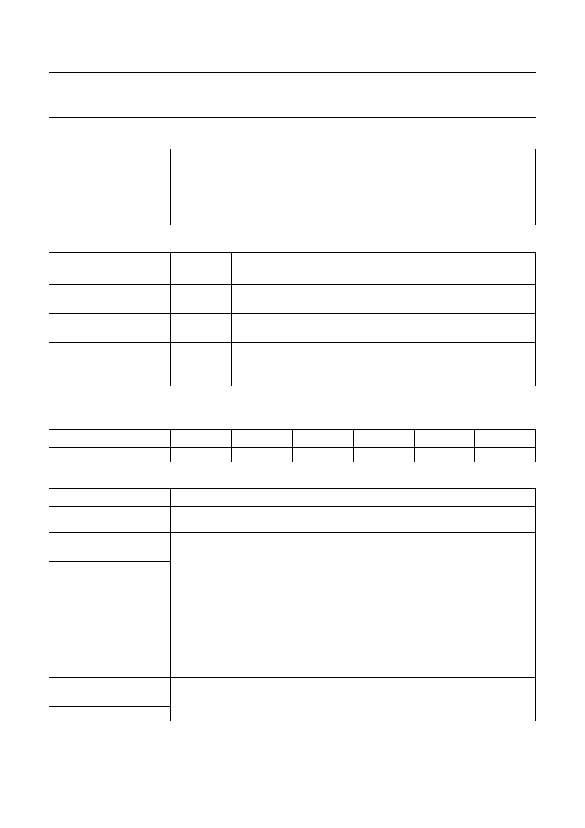
Philips Semiconductors Preliminary specification
Channel encoder/decoder CDR60 SAA7392
Table 74 Selection of coefficient K
i
Ki.1 Ki.0 COEFFICIENT K
0 0 3.1 × 10
0 1 6.1 × 10
1 0 1.2 × 10
1 1 2.4 × 10
Table 75 Selection of the coefficient K
−5
−5
−4
−4
f
Kf.2 Kf.1 Kf.0 COEFFICIENT K
0 0 0 reserved
0013.7×10
0107.5×10
0111.5×10
1003.0×10
1016.0×10
1101.2×10
1112.4×10
−9
−9
−8
−8
−8
−7
−7
7.10.3 MOTOR CONTROL REGISTER 7(MOTOR7)
Table 76 Motor Control Register 7 (address 1DH) - WRITE
i
f
76543210
PhErSrc − Kf’.2 Kf’.1 Kf’.0 Ki’.2 Ki’.1 Ki’.0
Table 77 Description of Motor7 bits
BIT SYMBOL DESCRIPTION
7 PhErSrc If PhErSrc = 0, then the phase error source is FIFOFil. If PhErSrc = 1, then the phase
error source is XError.
6 − This bit is reserved.
5 Kf’.2 These 3 bits select the value of the K
4 Kf’.1
3 Kf’.0
Kf’operates by sampling the input. For example, for Kf’= 1, every sample of the input is
passed through to a following integrator circuit, for a Kf’ of 0.5 every 2nd sample is
coefficient; see Table 78.
f’
passed through, for a Kf’ of 0.25 every 4th sample is passed through, and so on.
For a DC input signal, Kf× Kf’should always give the same result. If however, the input
is varying sufficiently quickly, the Kf× Kf’ combinations with the same product will not
always give the same result, especially for low values of Kf’, where the sampling in the
extreme becomes 1 out of every 128 samples. (The input samples to the block that
performs the Kf’multiplication occur at a rate of 1 sample every 24 system clock
periods.)
2 Ki’.2 These 3 bits select the value of the K
coefficient; see Table 78.
i’
1 Ki’.1
0 Ki’.0
2000 Mar 21 41
Page 42
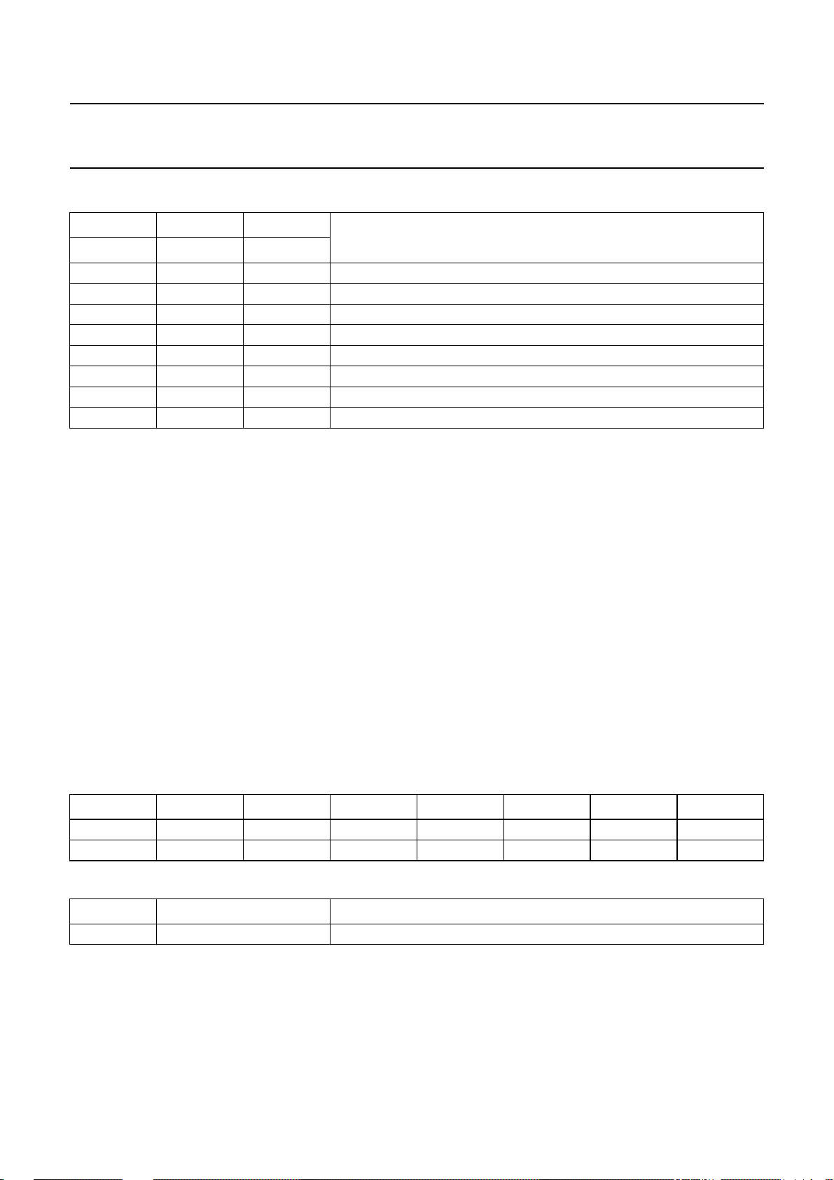
Philips Semiconductors Preliminary specification
Channel encoder/decoder CDR60 SAA7392
Table 78 Selection of coefficient Kf’ and K
i’
Kf’.2 Kf’.1 Kf’.0
Ki’.2 Ki’.1 Ki’.0
COEFFICIENTS K
AND K
f’
i’
0001
0010.5
0 1 0 0.25
0 1 1 0.125
1 0 0 0.0625
1 0 1 0.03125
1 1 0 0.015625
1 1 1 0.0078125
7.10.4 MOTOR CONTROL REGISTER 3(MOTOR3)
The function of this register is dependent upon whether its being read or written.
Whenwritten, thevalue determines theFIFO set-pointvalue inC1 frames (oneC1 frameis 24 bytes).The FIFO set-point
value should be set to a value greater than 110 frames for CD Fast mode and greater than 219 frames for CD Normal
mode. The maximum value for the FIFO half-full value is 256. Normally, the FIFO set-point value should be set to the
minimum value plus a margin for disc overspeed. The set-point value is calculated as shown below:
FIFO set-point value = HFSP<7:0> × 8.
When read, the motor speed can be determined from the recovered tacho frequency. Note this information is only valid
whena Hallmotor isbeing usedin theapplication andthe tacho subsystem is correctlyconfigured. Thereading isrelated
to the motor frequency (relative to pulse rate on a single tacho input pin) as shown in Equation (1); the actual Tacho
frequency can be calculated as shown in Equation (2). Negative frequencies will be measured if the motor is rotating in
reverse.
Tacho4
6 Tacho1×()Motor frequency×[]
=
---------------------------------------------------------------------------------------- Tacho sample rate
(1)
Tacho frequency (Hz) Tacho4
ADC clock
×=
--------------------------- 128
Table 79 Motor Control Register 3 (address 0EH) - WRITE/READ
76543210
HFSP.7 HFSP.6 HFSP.5 HFSP.4 HFSP.3 HFSP.2 HFSP.1 HFSP.0
TachoFreq.7 TachoFreq.6 TachoFreq.5 TachoFreq.4 TachoFreq.3 TachoFreq.2 TachoFreq.1 TachoFreq.0
Table 80 Description of Tacho4 bits for read operation
BIT SYMBOL DESCRIPTION
7 to 0 TachoFreq<7:0> These 8 bits indicate the Tacho frequency (2’s complement notation).
2000 Mar 21 42
(2)
Page 43
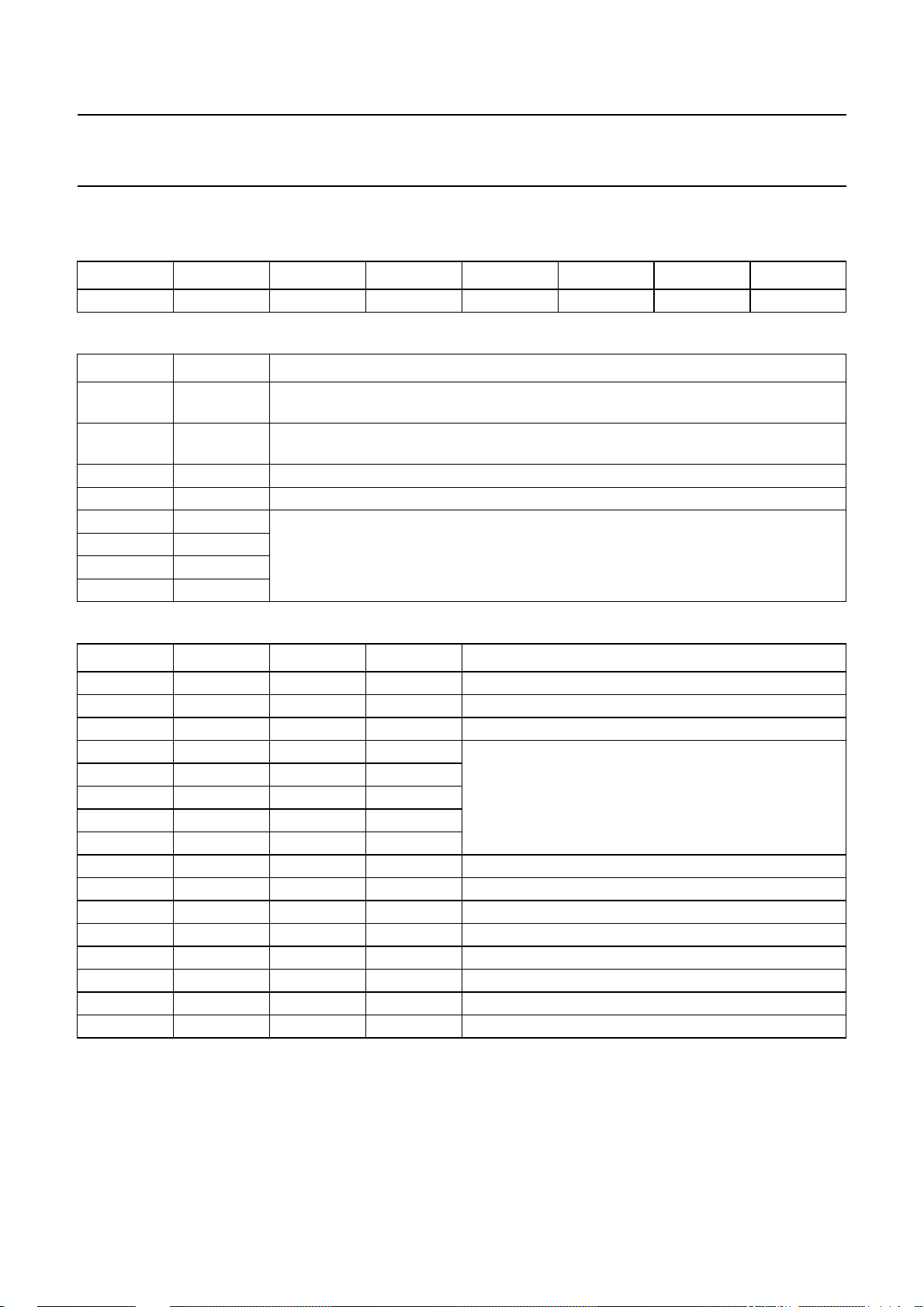
Philips Semiconductors Preliminary specification
Channel encoder/decoder CDR60 SAA7392
7.10.5 MOTOR CONTROL REGISTER 4(MOTOR4)
Table 81 Motor Control Register (address 0FH) - WRITE
76543210
PWM_PDM OVF_SW SW1 SW2 MSCON.3 MSCON.2 MSCON.1 MSCON.0
Table 82 Description of Motor4 bits
BIT SYMBOL DESCRIPTION
7 PWM_PDM If PWM_PDM = 0, then motor control in PWM mode. If PWM_PDM = 1, then motor
control in PDM mode.
6 OVF_SW If OVF_SW = 0, then SW1 and SW2 in normal operation. If OVF_SW = 1, then SW1
and SW2 will both open on overflow.
5 SW1 If SW1 = 0, then SW1 is open. If SW1 = 1, then SW1 is closed.
4 SW2 If SW2 = 0, then SW2 is open. If SW2 = 1, then SW2 is closed.
3 MSCON.3 These 4 bits are used to select the motor servo state; see Table 83.
2 MSCON.2
1 MSCON.1
0 MSCON.0
Table 83 Selection of motor servo state
MSCON.3 MSCON.2 MSCON.1 MSCON.0 MOTOR SERVO STATE
0 0 0 0 Motor servo active.
0 0 0 1 Motor servo off (clears integrator).
0 0 1 0 Motor servo 3-state (motor output pin 3-states).
0 0 1 1 These 5 codes are reserved.
0100
0101
0110
0111
1 0 0 0 Motor start at 37% power.
1 0 0 1 Motor start at 50% power.
1 0 1 0 Motor start at 75% power.
1 0 1 1 Motor start at 100% power.
1 1 0 0 Motor stop at 37% power.
1 1 0 1 Motor stop at 50% power.
1 1 1 0 Motor stop at 75% power.
1 1 1 1 Motor stop at 100% power.
2000 Mar 21 43
Page 44
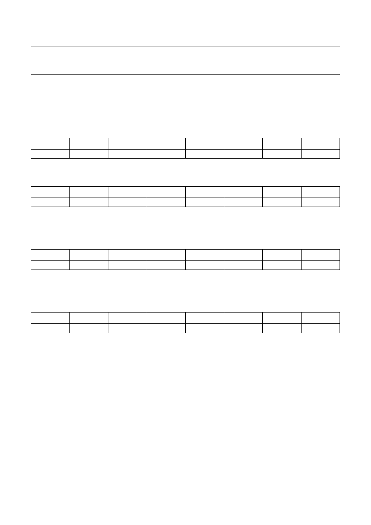
Philips Semiconductors Preliminary specification
Channel encoder/decoder CDR60 SAA7392
7.10.6 MOTOR CONTROL REGISTERS 5 AND 6
These two registers hold the 16-bit motor integrator value. The motor integrator value can be read or updated using
registers Motor5 and Motor6. Register Motor5 should be read or written first to prevent spurious results.
7.10.6.1 Motor Control Register 5 (Motor5)
Table 84 Motor Control Register 5 (address 10H) - READ/WRITE
76543210
MIV.7 MIV.6 MIV.5 MIV.4 MIV.3 MIV.2 MIV.1 MIV.0
7.10.6.2 Motor Control Register 6 (Motor6)
Table 85 Motor Control Register 6 (address 11H) - READ/WRITE
76543210
MIV.15 MIV.14 MIV.13 MIV.12 MIV.11 MIV.10 MIV.9 MIV.8
7.10.7 T
This register holds the 8-bit Tacho multiplier frequency value.
Table 86 Tacho Gain Setting Register (address 17H) - WRITE
KTacho.7 KTacho.6 KTacho.5 KTacho.4 KTacho.3 KTacho.2 KTacho.1 KTacho.0
7.10.8 T
This register holds the 8-bit Tacho interrupt trip frequency value.
Table 87 Tacho Trip Setting Register (address 18H) - WRITE
ACHO GAIN SETTING REGISTER (TACHO1)
76543210
ACHO TRIP SETTING REGISTER (TACHO2)
76543210
TIntF.7 TIntF.6 TIntF.5 TIntF.4 TIntF.3 TIntF.2 TIntF.1 TIntF.0
2000 Mar 21 44
Page 45
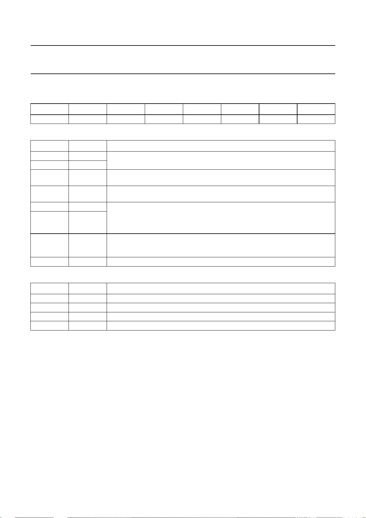
Philips Semiconductors Preliminary specification
Channel encoder/decoder CDR60 SAA7392
7.10.9 TACHO CONTROL REGISTER 3(TACHO3)
Table 88 Tacho Control Register 3 (address 19H) - WRITE
76543210
SConS.1 SConS.0 TachoFRes Moto2/T3 Fsam.1 Fsam.0 TachoIntLF TachoMode
Table 89 Description of Tacho3 bits
BIT SYMBOL DESCRIPTION
7 SConS.1 These 2 bits select the motor servo frequency source; see Table 90.
6 SConS.0
5 TachoFRes IfTachoFRes = 0, thenthe tacho filteris enabled (normal mode).If TachoFRes = 1, then
the tacho filter is reset.
4 Moto2/T3 If Moto2/T3 = 0, then MOTO2 pin is an output. If Moto2/T3 = 1, then MOTO2 pin is
tacho T3.
3 Fsam.1 These 2 bits select the tacho sample rate (f
2 Fsam.0
fsHz()
1 TachoIntLF If TacholntLF = 0, then tacho interrupt isenabled on frequenciesLOWER than set-point.
If TacholntLF = 1, then tacho interrupt is enabled on frequencies HIGHER than
set-point.
0 TachoMode If TachoMode = 0, tacho is in 3-pin mode. If TachoMode = 1, tacho is in 1-pin mode.
2
2
Fsam<1:0>× system clock×
=
----------------------------------------------------------------------------------32768
) as shown below:
s
Table 90 Motor servo frequency source selection
SConS.1 SConS.0 MOTOR SERVO FREQUENCY SOURCE
0 0 Motor servo locks to PLL clock (recovered from channel EFM).
0 1 This value is reserved.
1 0 Motor servo runs on tacho frequency.
1 1 This value is reserved.
2000 Mar 21 45
Page 46
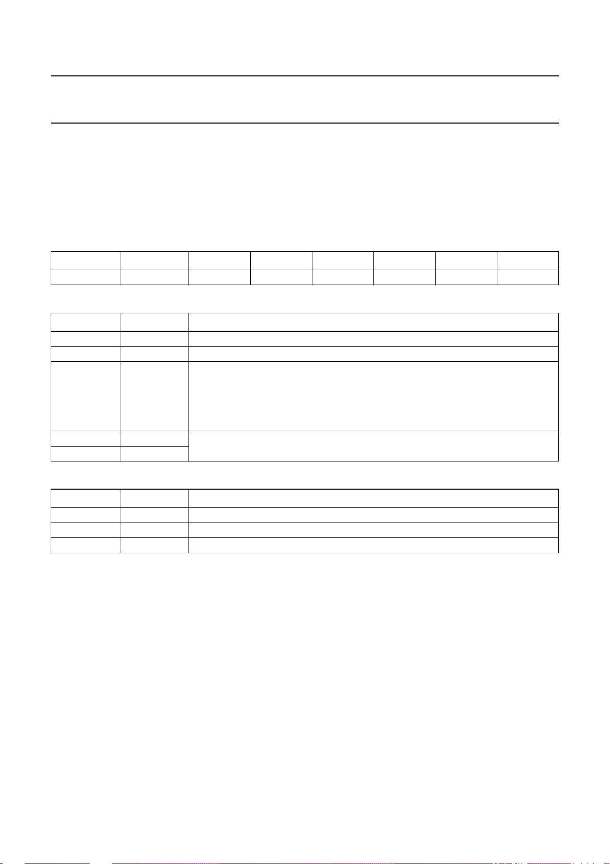
Philips Semiconductors Preliminary specification
Channel encoder/decoder CDR60 SAA7392
7.11 The serial in function
The serialin function takes serial data from the block decoder andpasses the dataon to the encoder. It supports theI2S
and Sony 3-wire serial interfaces (DATAI, BCLK and WCLK). The block is slave to the interface and therefore the BCLK
and WCLK signals are generated externally and are the same signals as the serial data output interface. The selection
of the input format follows the output interface setting.
7.11.1 INPUT CONFIGURATION REGISTER (INPUTCONFIG)
Table 91 Input Configuration Register (address 1EH) - WRITE
7 6 543210
EBUClkSelect − −−−ScramOn InputFmt.1 InputFmt.0
Table 92 Description of InputConfig bits
BIT SYMBOL DESCRIPTION
7 EBUClkSelect See Section 7.8.1.
6to3 − These 4 bits are reserved.
2 ScramOn This bit enables/disables the scrambling function. If ScramOn = 1, then the
scrambling function is enabled.
Scrambling must be off for CD-DA and on for CD-ROM. However, if the buffer
manager (block decoder) already scrambles the CD-ROM data, then the user must
switch scrambling off in the CDR60.
1 InputFmt.1 These 2 bits select the input format to the encoder; see Table 93.
0 InputFmt.0
Table 93 Selection of encoder input format
INPUTFMT.1 INPUTFMT.0 INPUT FORMAT
0 0 normal input data to encoder
0 1 all zero input data to encoder
1 X random input data to encoder
2000 Mar 21 46
Page 47

Philips Semiconductors Preliminary specification
Channel encoder/decoder CDR60 SAA7392
7.12 The subcode insert function
The SAA7392 allows two modes of subcode insertion:
Bypass mode and Auto-format mode.
• Bypass mode. In this mode the subcode is generated
by a block decoder (such as PLUM) and transmitted to
the SAA7392 via the proprietary Subcode Record
Interface (SRI). P, Q and R to W channels are
supported in this mode. However, the Q-channel CRC
and the S0 and S1 bytes are generated by the
SAA7392. The Q-channel CRC is calculated from the
SRI data Q-bits and hence the 16 Q-channel CRC bits
in the SRI data are discarded.
• Auto-format mode. In this mode, the SAA7392 will
generate subcode data itself. However, only
P and Q subcode channels are supported.
7.12.1 SUBCODE PRESET COUNT REGISTER (SUBPRESETCOUNT)
The presetcount field isloaded when thisregister is written. The current count field is returned when this register is read.
Table 94 Subcode Preset Count Register (address 22H) - WRITE
76543210
init_frame PCF.6 PCF.5 PCF.4 PCF.3 PCF.2 PCF.1 PCF.0
It is possibleto beginsubcode recordingat anypoint inthe
subcode frame, for both internally and externally
generated subcode, by loading the preset count field (bits
PCF<6:0> in the SubPresetCount register) with the start
positionin thesubcode frameand settingthe init_framebit
to a logic 1.
Itmust beensured that,if used, theexternal blockencoder
is ready to transmit subcode data before the frame
initialisation is started. When the frame initialisation
sequence is complete the init_frame bit is automatically
cleared to a logic 0.
It should be noted that the frame initialisation sequence
must be carried out at the beginning of every record
session, even if starting from byte 0.
Table 95 Subcode Preset Count Register (address 22H) - READ
76543210
init_frame CCF.6 CCF.5 CCF.4 CCF.3 CCF.2 CCF.1 CCF.0
2000 Mar 21 47
Page 48
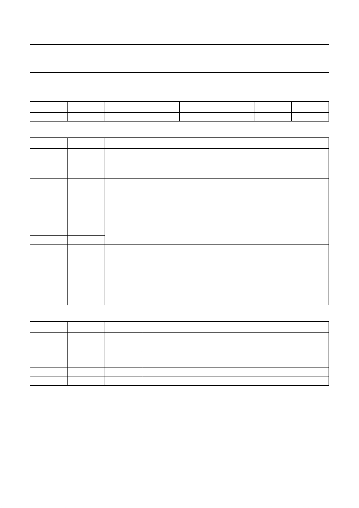
Philips Semiconductors Preliminary specification
Channel encoder/decoder CDR60 SAA7392
7.12.2 SUBCODE CONFIGURATION REGISTER 1(SUBCONFIG1)
Table 96 Subcode Configuration Register 1 (address 23H) - WRITE
76543210
sri_on p_toggle p_one time1 time2 copy_alter zero_inc time3
Table 97 Description of SubConfig1 bits
BIT SYMBOL DESCRIPTION
7 sri_on If sri_on = 0, then subcode generated by CDR60 for Pand Q-channels; R to W
channels are all logic 0’s. If sri_on = 1, then subcode data from SRI except Q-channel
CRC and S0 and S1 bytes. SRI frame sync checking is enabled. SubConfig1 register
bits 1 to 6 do not effect the SRI subcode data.
6 p_toggle If p_toggle = 0, then P-channel takes value of the p_one bit. If p_toggle = 1, then
P-channel is the value of bit 5 of the absolute frame byte in the current Q-code memory
bank.
5 p_one P-channel is the value of this bit. The P-channel takes on a new value of p_one at the
start of a subcode frame.
4 time1 These 3 bits control the incrementing and decrementing of the Q-channel absolute and
3 time2
0 time3
2 copy_alter If copy_alter = 0, then the copy bit will hold its current value. The copy bit value can be
1 zero_inc If zero_inc = 0, then all bits of the Q-code memory zero byte will hold. If zero_inc = 1,
relative time fields; see Table 98.
changed by writing to the Q-code memory control byte via the SubData register. If
copy_alter = 1, then the copy bit in the subcode control byte will alternate every
4 subcode frames. This is accomplished by copyingbit 2 of the current Q-code memory
absolute frame byte to the copy bit of the Q-code memory control byte.
then bits 0 to 3 of the current Q-code memory zero byte are incremented modulo 10.
Bits 4 to 7 are unchanged.
Table 98 Selection of Q-channel time fields
time3 time2 time1 Q-CHANNEL TIME FIELD
0 0 0 increment relative and absolute time
0 1 1 increment relative time and hold absolute time
1 0 0 hold relative time and increment absolute time
1 0 1 decrement relative time and increment absolute time
1 1 1 hold relative and absolute time
X X X All other settings are reserved.
2000 Mar 21 48
Page 49
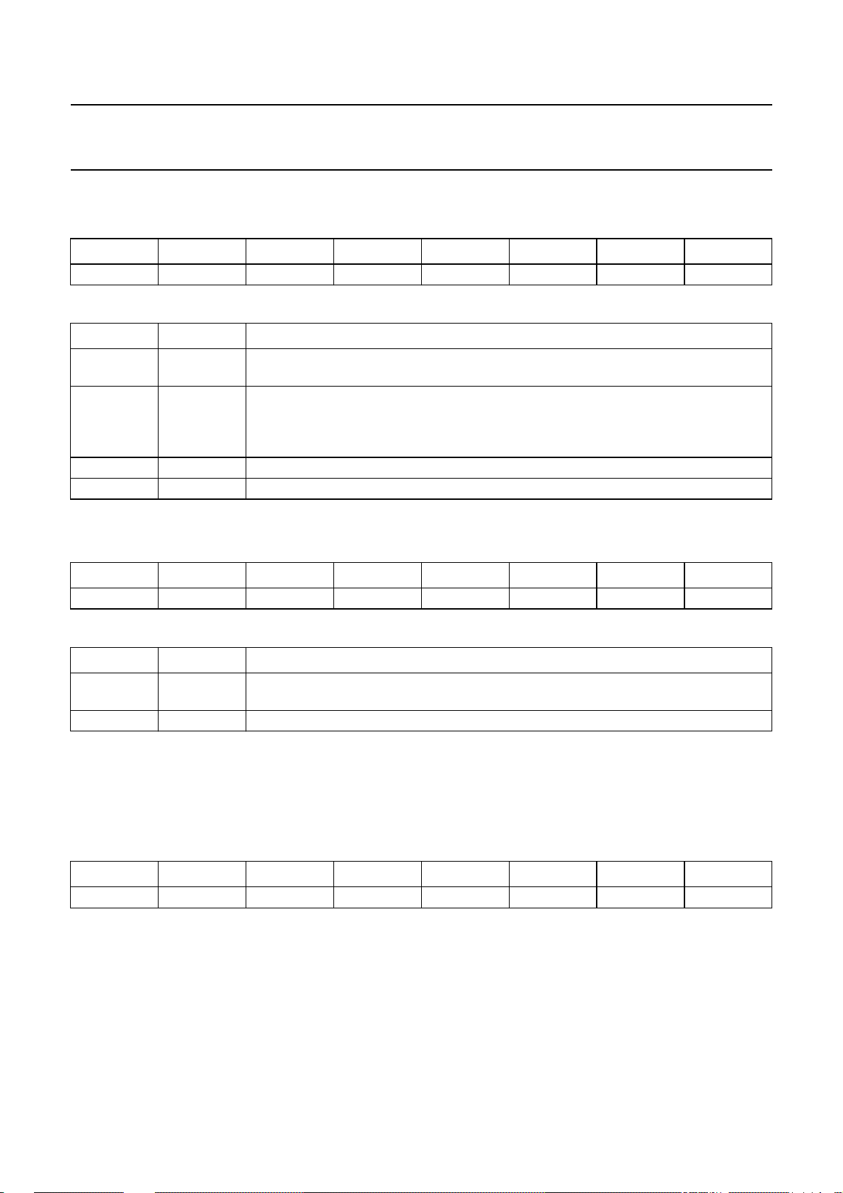
Philips Semiconductors Preliminary specification
Channel encoder/decoder CDR60 SAA7392
7.12.3 SUBCODE CONFIGURATION REGISTER 2(SUBCONFIG2)
Table 99 Subcode Configuration Register 2 (address 24H) - READ/WRITE
76543210
BSwOn InOBO relcnt.2 relcnt.1 relcnt.0 curcnt.2 curcnt.1 curcnt.0
Table 100 Description of SubConfig2 bits
BIT SYMBOL DESCRIPTION
7 BSwOn If BSwOn = 0, then no bank switching. If BSwOn = 1, then bank switch will occur when
first subcode sync output by EFM modulator and curcnt<2:0> = 000
6 InOBO If InOBO = 0, then original bank is used again. In this case no bank switching or
interrupts occur andautomatic bank update isstill done on theoriginal bank, evenwhen
the other bank is output. If InOBO = 1, then the other bank is automatically inserted
once into Q-channel, this bit is automatically reset to logic 0.
5 to 3 relcnt<2:0> Count value to load curcnt<2:0>.
2 to 0 curcnt<2:0> Current value of subcode frame counter.
7.12.4 S
Table 101 Subcode Start Data Register (address 25H) - WRITE
Table 102 Description of SubStartData bits
7.12.5 S
Sub-CPU read/write from/to the SubData register causes a read or write to occur on the Q-code memory. Normally the
sub-CPU would access all 10 bytes of a Q-code bank. Before such a block access the sub-CPU must issue a write to
the SubStartWrite register.
Table 103 Subcode Data Register (address 26H) - READ/WRITE
UBCODE START DATA REGISTER (SUBSTARTDATA)
76543210
NextSet −−−−−−−
BIT SYMBOL DESCRIPTION
7 NextSet If NextSet = 0, then access other bank. If NextSet = 1, then access current bank that is
being used for Q-channel data.
6to0 − These 7 bits are reserved.
UBCODE DATA REGISTER (SUBDATA)
76543210
QCD.7 QCD.6 QCD.5 QCD.4 QCD.3 QCD.2 QCD.1 QCD.0
2000 Mar 21 49
Page 50

Philips Semiconductors Preliminary specification
Channel encoder/decoder CDR60 SAA7392
7.12.6 GENERATING CD-TEXT
CD-Text is stored in the R to W channels of the disc. The
CD-Text standardstates that aCD-Text disc must at least
contain CD-Text information in the lead-in, and it may
contain CD-Text information in the program area.
CDR60 supports writing of the R to W subcode channels
only in bypass modewhich meansthat thewhole subcode
informationhas tobe generatedfrom anexternal device.It
is not possible to use the automatic subcode formatting
features like auto-incrementing or the two buffers which
means that the application has to take care of the whole
subcode formatting itself. However, if an application likes
to write a CD-Text disc that contains CD-Text information
only in the lead-in area, then the application can use the
auto-format featuresfor writing theprogram area and only
use the bypass mode to write CD-Text information when
writing the lead-in.
7.14.1 ENCODE WRITEON CONTROL REGISTER (ENCODEWCON)
Table 104 Encode WriteOn Control Register (address 30H) - READ/WRITE
76543210
WriteOn1 WriteOn2 EFMDelOn Count.4 Count.3 Count.2 Count.1 Count.0
7.13 The data encoder block
Thisblock generatesall C1/C2 errorcorrection datafor the
raw data.
7.14 Encode control block
This block controlsthe starting and stopping of the writing
process. It does this based on the QSync signal it receives
from the subcode insert block and the ATIPSync and
W441disc positioninformation itreceivesfrom theWobble
processor.
Table 105 Description of EncodeWContr bits
BIT SYMBOL DESCRIPTION
7 WriteOn1 If WriteOn1 = 0, then laser is off or turn laser off. If WriteOn1 = 1,then laser is onor turn
laser on.
6 WriteOn2 If WriteOn2 = 0, then data flowis off or turn dataflow off. If WriteOn2 = 1, then data flow
is on or turn data flow on.
5 EFMDelOn If EFMDelOn = 0, then disable delay of WriteOn1. If EFMDelOn = 1, then enable delay
of WriteOn1 with EncodeStartOffset/EncodeStopOffset of W441 pulses relative to
ATIPSync.
4 Count.4 These 5 bits determine the delay generation of internal WriteOn flags by Count<4:0>
3 Count.3
2 Count.2
1 Count.1
0 Count.0
ATIPSyncs.
2000 Mar 21 50
Page 51
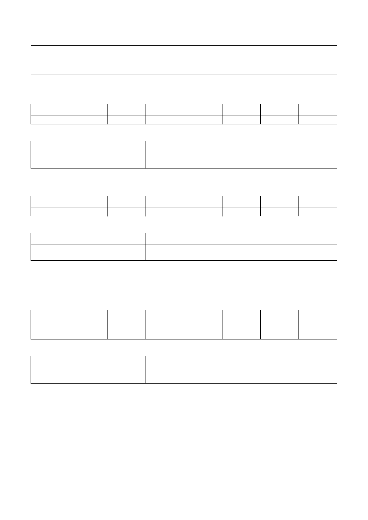
Philips Semiconductors Preliminary specification
Channel encoder/decoder CDR60 SAA7392
7.14.2 ENCODE START OFFSET REGISTER (ENCODESTARTOFFSET)
Table 106 Encode Start Offset Register (address 31H) - WRITE
76543210
StartOffset.7 StartOffset.6 StartOffset.5 StartOffset.4 StartOffset.3 StartOffset.2 StartOffset.1 StartOffset.0
Table 107 Description of EncodeStartOffset bits
BIT SYMBOL DESCRIPTION
7 to 0 StartOffset<7:0> If enabled, WriteOn flags are delayed by EncodeStartOffset pulses of
W441 when starting the encode process.
7.14.3 ENCODE STOP OFFSET REGISTER (ENCODESTOPOFFSET)
Table 108 Encode Stop Offset Register (address 32H) - WRITE
76543210
StopOffset.7 StopOffset.6 StopOffset.5 StopOffset.4 StopOffset.3 StopOffset.2 StopOffset.1 StopOffset.0
Table 109 Description of EncodeStopOffset bits
BIT SYMBOL DESCRIPTION
7 to 0 StopOffset<7:0> If enabled, WriteOn flags are delayed by EncodeStopOffset pulses of
W441 when stopping the encode process.
7.14.4 ENCODE XOFFSET REGISTER (ENCODEXOFFSET)
The 10-bit value for Xoffset must be written in two steps. EncodeXOffset can be written to in any order. XOffset<9:0> is
a 2’s complement number which gives a range of −511 to 511.
Table 110 Encode XOffset Register (address 33H) - WRITE
76543210
0 0 XOffset.5 XOffset.4 XOffset.3 XOffset.2 XOffset.1 XOffset.0
01−−XOffset.9 XOffset.8 XOffset.7 XOffset.6
Table 111 Description of EncodeXoffset bits
BIT SYMBOL DESCRIPTION
7 to 0 XOffset<9:0> Offset applied to the phase error calculated between ATIPSync and
Q-code sync.
2000 Mar 21 51
Page 52
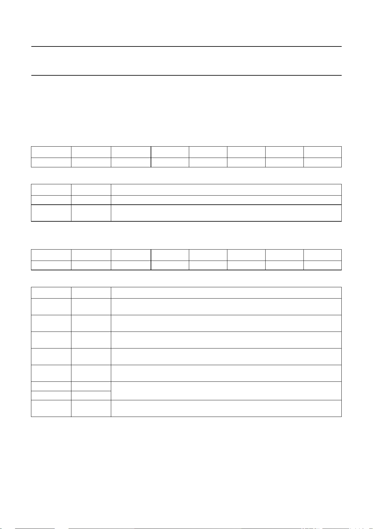
Philips Semiconductors Preliminary specification
Channel encoder/decoder CDR60 SAA7392
7.15 The EFM modulator
This block takes data from the data encoder block and adds the subcode and synchronisation information. This data
stream ismodulated usingEFM according tothe Red Book standard. Thisdata is outputserially fromthe SAA7392, with
the associated EFM clock signal.
7.15.1 EFM PRESET COUNT REGISTER (EFMPRESETCOUNT)
Table 112 EFM Preset Count Register (address 3CH) - WRITE
7 6 543210
−−Count.5 Count.4 Count.3 Count.2 Count.1 Count.0
Table 113 Description of EFMPresetCount bits
BIT SYMBOL DESCRIPTION
7 and 6 − These 2 bits are reserved.
5 to 0 Count<5:0> Thisfield can be used to program a position in an EFM frame for the modulator to start
outputting data.
7.15.2 EFM M
Table 114 EFM Modulator Configuration Register (address 3DH) - WRITE
7 6 543210
EFMClkSel ModifiedEFM EnableLWRT LWRTOn GateClkOn DataSel.1 DataSel.0 PanicOn
Table 115 Description of EFMModConfig bits
BIT SYMBOL DESCRIPTION
7 EFMClkSel If EFMClkSel = 0, then EFM clock generator outputs normal XEFM frequency clock. If
6 ModifiedEFM If ModifiedEFM= 0, then normal EFM output. If ModifiedEFM = 1, then all ‘0’ output
5 EnableLWRT If EnableLWRT = 0, then LaserOn is off. If EnableLWRT = 1, then LaserOn will be set
4 LWRTOn If LWRTOn = 0, then LaserOn determined by EnableLWRT bit. If LWRTOn = 1, then
3 GateClkOn If GateClkOn = 0, then XEFM clock is on if WriteOn2 is set. If GateClkOn = 1, then
2 DataSel.1 These 2 bits along with the DataSel.2 bit in register EFMCON2 select the output data
1 DataSel.0
0 PanicOn If PanicOn = 1, the Panic input is enabled. LaserOn will be disabled immediately when
ODULATOR CONFIGURATION REGISTER (EFMMODCONFIG)
EFMClkSel = 1, then EFM clock generator outputs double frequency XEFM clock.
symbols are increased in length by one bit.
when WriteOn1 is turned on.
LaserOn output is enabled unconditionally.
XEFM clock is gated on unconditionally.
format; see Table 119.
the PANIC pin (pin 27) is logic 1.
2000 Mar 21 52
Page 53
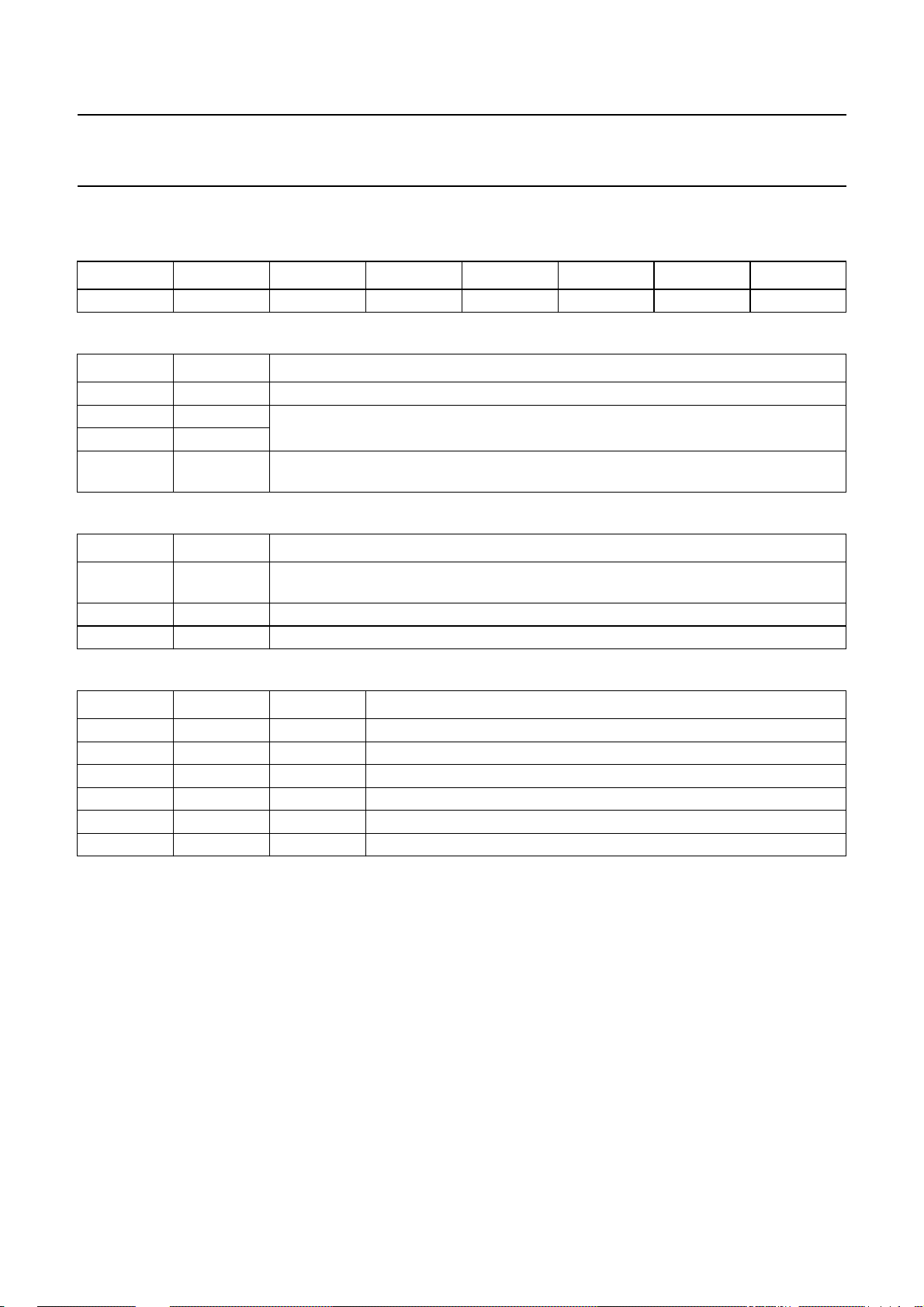
Philips Semiconductors Preliminary specification
Channel encoder/decoder CDR60 SAA7392
7.15.3 EFM MODULATOR CONFIGURATION REGISTER 2 (EFMMODCONFIG2))
Table 116 EFM Modulator Configuration Register 2 (address 3EH) - WRITE
76543210
−−−−−TIM2Mode TIM2ClkOn DataSel.2
Table 117 Description of EFMModConfig2 bits
BIT SYMBOL DESCRIPTION
7to3 − These 5 bits are reserved.
2 TIM2Mode These 2 bits control the XEFM output; see Table 118.
1 TIM2ClkOn
0 DataSel.2 This bit along with the DataSel.1 and DataSel.0 bits in register EFMModConfig select
the output data format; see Table 119.
Table 118 Control of the XEFM output
TIM2Mode TIM2ClkOn
0 X XEFM is operated according to GateClkOn bit setting in the EFMCON register
(address 3DH).
1 0 XEFM output is not influenced by LaserOn/WriteOn and is off.
1 1 XEFM is gated on.
Table 119 Selection of output data format
DataSel.2 DataSel.1 DataSel.0 OUTPUT DATA FORMAT
0 0 0 hold data output at zero
0 0 1 output normal data
0 1 0 output I3 pattern
0 1 1 output I11 pattern
1 0 1 output special OPC pattern 3-3-4-4-5-5-6-6-7-7
X X X All other settings are reserved.
2000 Mar 21 53
Page 54
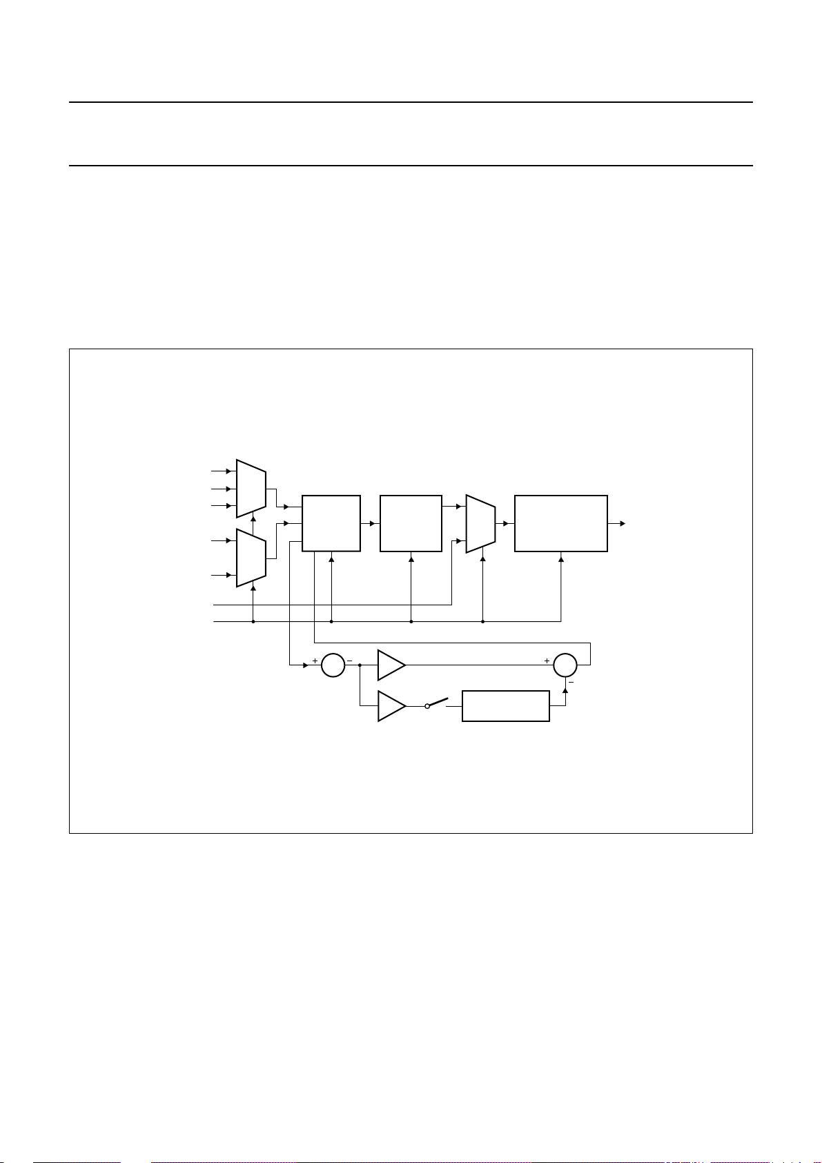
Philips Semiconductors Preliminary specification
Channel encoder/decoder CDR60 SAA7392
7.16 The EFM clock generator
TheEFM clockgenerator willproduce the recordingclock basedon one ofthree referencesources. Therearefive stages
to the function. The first selects the reference source using a multiplexer. The next stage is a digital PLL to up-multiply
the reference source. The source will determine the base frequency output by the PLL, whilst a position error signal is
used to alter the frequency sothat the position errortends to zero. Next,an analog PLL isused to up-multiply theoutput
from the digital PLL. The output of the analog PLL is then multiplexed with an external source to allow the EFM clock
generator to be bypassed completely. Finally, a programmable divider is used to enable the clock output, XEFM, to be
doubled producing XEFM_2.
handbook, full pagewidth
W441
WCLK
Sysclk/192
XError
Fifo filling
Sysclk
Config Data
MUX
MUX
DIGITAL
PLL
+
ANALOG
PLL
K
p
K
i
MUX XEFM
INTEGRATOR
Fig.18 EFM PLL block diagram.
PROGRAMMABLE
DIVIDER
+
MGR808
2000 Mar 21 54
Page 55
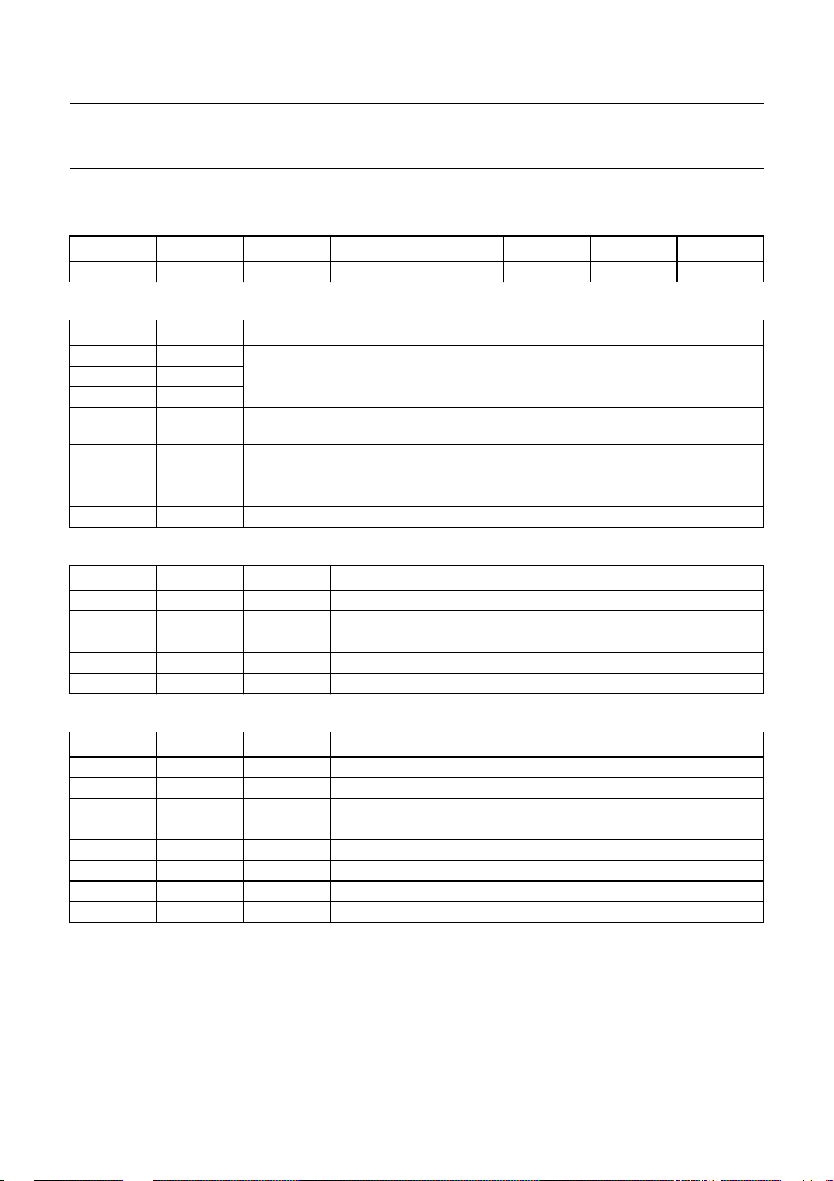
Philips Semiconductors Preliminary specification
Channel encoder/decoder CDR60 SAA7392
7.16.1 EFM CLOCK CONFIGURATION REGISTER 1 (EFMCLOCKCONF1)
Table 120 EFM Clock Configuration Register 1 (address 34H) - WRITE
76543210
DPLLBW.2 DPLLBW.1 DPLLBW.0 Bypass Div.2 Div.1 Div.0 −
Table 121 Description of EFMClockConf1 bits
BIT SYMBOL DESCRIPTION
7 DPLLBW.2 These 3 bits select the digital PLL bandwidth; see Table 122.
6 DPLLBW.1
5 DPLLBW.0
4 Bypass When Bypass = 0, then bypass is off. When Bypass = 1, then PLL is bypassed and the
XEFM clock is derived from the system clock.
3 Div.2 These 3 bits select the analog PLL output divisor; see Table 123.
2 Div.1
1 Div.0
0 − This bit is reserved.
Table 122 Selection of PLL bandwidth
DPLLBW.2 DPLLBW.1 DPLLBW.0 PLL BANDWIDTH
0 0 0 Digital PLL bandwidth is 400 Hz.
0 0 1 Digital PLL bandwidth is 200 Hz.
0 1 0 Digital PLL bandwidth is 100 Hz.
0 1 1 Digital PLL bandwidth is 50 Hz.
1 0 0 Digital PLL bandwidth is 25 Hz.
Table 123 Selection of analog PLL output divisor
Div.2 Div.1 Div.0 PLL DIVISOR
0 0 0 Analog PLL output is divided by 1 (XEFM_2 output is not available).
0 0 1 Analog PLL output is divided by 2.
0 1 0 Analog PLL output is divided by 3 (XEFM_2 output is not available).
0 1 1 Analog PLL output is divided by 4.
1 0 0 Analog PLL output is divided by 6.
1 0 1 Analog PLL output is divided by 8.
1 1 0 Analog PLL output is divided by 12.
1 1 1 Analog PLL output is divided by 16.
2000 Mar 21 55
Page 56
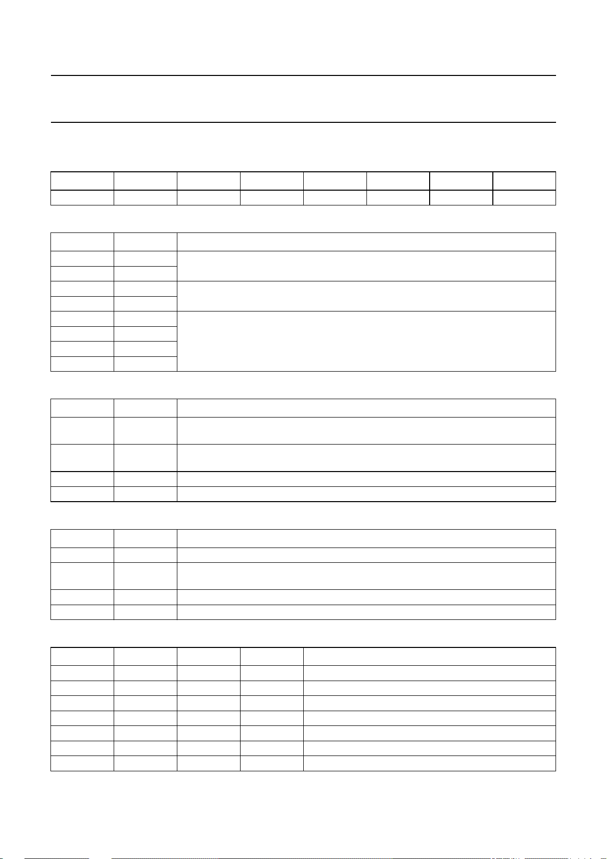
Philips Semiconductors Preliminary specification
Channel encoder/decoder CDR60 SAA7392
7.16.2 EFM CLOCK CONFIGURATION REGISTER 2 (EFMCLOCKCONF2)
Table 124 EFM Clock Configuration Register 2 (address 35H) - WRITE
76543210
FreqSrc.1 FreqSrc.0 PosSrc.1 PosSrc.0 DPLLMF.3 DPLLMF.2 DPLLMF.1 DPLLMF.0
Table 125 Description of EFMClockConf2 bits
BIT SYMBOL DESCRIPTION
7 FreqSrc.1 These 2 bits select the frequency source for the PLL; see Table 126.
6 FreqSrc.0
5 PosSrc.1 These 2 bits select the position source; see Table 127.
4 PosSrc.0
3 DPLLMF.3 These 4 bits select the multiplication factor for the PLL; see Table 128
2 DPLLMF.2
1 DPLLMF.1
0 DPLLMF.0
Table 126 Selection of PLL frequency source
FreqSrc.1 FreqSrc.0 FREQUENCY SOURCE
0 0 PLL locks to W441. Use this signal as frequency source to lock EFM frequency to disc
wobble.
0 1 PLL locks to WCLK. Use this signal if encoding must slave to the word clock of some
external I
1 0 PLL locks to sysclock/192
1 1 This setting is reserved.
Table 127 Selection of position source
PosSrc.1 PosSrc.0 POSITION SOURCE
0 0 No position error used.
1 0 Position source is XError<6:0>. Use this source if EFM clock is locked to ATIP carrier
(W441).
1 1 Position source is FifoFill<6:0>. Use this source is EFM clock is locked to WCLK signal.
X X All other combinations are reserved.
Table 128 Digital PLL multiplication factor
DPLLMF.3 DPLLMF.2 DPLLMF.1 DPLLMF.0 DIGITAL PLL MULTIPLICATION FACTOR
0000294
0001196
0010147
010098
0 1 1 0 73.5
100049
1 0 1 0 36.75
2
S/EBU input.
2000 Mar 21 56
Page 57
Philips Semiconductors Preliminary specification
Channel encoder/decoder CDR60 SAA7392
7.16.3 EFM CLOCK CONFIGURATION REGISTER 3 (EFMCLOCKCONF3)
This is a dual-function register, the specific function is controlled by the state of bit 7.
The integrator of the PI controller can be preset by writing to this register with the MSB set to logic 0. The value written
is interpreted as a signed value. The current integrator value can be read back via this register.
To program the Kp and Ki values, bit 7 of the EFMClockConf3 register must be logic 1.
To determine the time constant of the I-branch, the sample frequency of the integrator must be known. This sample
frequency is programmed via register EFMClockConf4 when the MSB is logic 1. The LSB is actually the switch to turn
off the integrator path. The value in the integrator is not affected by programming this bit, so the integrator can be used
as offset when Ki is logic 0.
Table 129 EFM Clock Configuration Register 3 (address 36H) - READ/WRITE
76543210
0 IntegVal.6 IntegVal.5 IntegVal.4 IntegVal.3 IntegVal.2 IntegVal.1 IntegVal.0
1 Kp.2 Kp.1 Kp.0 Ki.3 Ki.2 Ki.1 Ki.0
Table 130 Selection of coefficient K
p
Kp.2 Kp.1 Kp.0 COEFFICIENT K
0004
0012
0101
0110.5
1 0 0 0.25
Table 131 Selection of the coefficient K
i
Ki.3 Ki.2 Ki.1 Ki.0 COEFFICIENT K
00000
00011
00110.5
0 1 0 1 0.25
0 1 1 1 0.125
1 0 0 1 0.0625
1 0 1 1 0.03125
1 1 0 1 0.015625
1 1 1 1 0.0078125
p
i
2000 Mar 21 57
Page 58
Philips Semiconductors Preliminary specification
Channel encoder/decoder CDR60 SAA7392
7.16.4 EFM CLOCK CONFIGURATION REGISTER 4
(EFMCLOCKCONF4)
This is a dual-function register, the specific function is
controlled by the state of bit 7.
The sample rate of the integrator may be programmed by
writing to this register when the MSB is set to a logic 1.
Higher sample rates let the integrator work faster. This is
effectively the same as increasing the Ki value.
Table 132 EFM Clock Configuration Register 4 (address 37H) - WRITE
7 6 5432 1 0
1 − −−−−Samplerate.1 Samplerate.0
0 PosErr.6 PosErr.5 PosErr.4 PosErr.3 PosErr.2 PosErr.1 PosErr.0
Table 133 Selection of the integrator sample rate
Samplerate.1 Samplerate.0 SAMPLE RATE
0 0 392
0 1 196
1098
1149
Good stability and criticaldamping ofthe integratorcan be
expected with a sample rate of1/98EFM frames and
Ki= 2-7at n = 2.
Theposition errorset-pointmay beprogrammedby writing
to thisregister when theMSB is set to a logic 0. Aposition
error setpoint between −64 and 63 can be programmed
using the remaining 7 bits.
On reset this register has the value −8.
Table 134 EFMPLL settings information
INTENDED
ENCODER SPEED
n = 1 294 4 12 2581 ms
n = 2 147 4 6 635 ms
n = 4 98 4 4 160 ms
DIGITAL
MULTIPLICATION
FACTOR
ANALOG PLL
MULTIPLICATION
FACTOR
PROGRAMMABLE
DIVIDER FACTOR
POSITION ERROR
TIME CONSTANT
2000 Mar 21 58
Page 59
Philips Semiconductors Preliminary specification
Channel encoder/decoder CDR60 SAA7392
7.17 The Wobble processor
The Wobble processor is a critical part of the recording
process, and performs two main functions:
• To extract the ATIP data from the wobble signal
• To control the linear disc speed during recording.
The Wobble processor comprises four functions, a
front-end ADC,a digital PLL, the ATIPbit detector andthe
ATIP data read interface.
7.17.1 THE WOBBLE ADC FUNCTION
This converts the ATIP signal (WIN) to the digital domain.
7.17.2 THE WOBBLE PLL
ThePLL hasaPI typeloopfilter. Thebandwidthof theloop
andthe integratorareprogrammable bythe user. Theuser
can also read andwrite thePLL frequency,the write mode
is available to aid PLL lock-in. The block outputs a pulse
signal at 44.1 kHz, which is phase modulatedby the ATIP
signal.
7.17.5 WOBBLE CONFIGURATION REGISTER 1(WOBBLECONFIG1)
This is adual-function register, the specific function is determined by the state of bit 7. When bit 7 = 0, the function is as
described in Tables 135 to 138. When bit 7 = 1, the function is as described in Tables 135 and 139.
7.17.3 THE ATIP BIT DETECTOR
This function extracts the ATIP information bits from the
ADC output and passes them to the ATIP read interface
block. It also outputs the ATIPSync pulse. In order to
protect the ATIPSyncs, a flywheel mechanism exists to
interpolate ATIPSyncs if none are detected. This is a
requirement to ensure thatthe recordingprocess doesnot
get corrupted.
7.17.4 THE ATIP READ INTERFACE
TheATIP datais readby the on-chipmicroprocessor. Data
availability can be checked by polling the ATIPReady bit in
the ATIP Status Register. The microprocessor must read
both the ATIPDataand ATIPDataEnd registers in orderto
complete the data read process correctly. If this does not
happen, a status bit is set to warn the microcontroller.
Table 135 Wobble Configuration Register 1 (address 27H) - WRITE
76543210
0 0 PLLIntBW.2 PLLIntBW.1 PLLIntBW.0 LoopBW.2 LoopBW.1 LoopBW.0
1 ATIPhold − WinWidth.4 WinWidth.3 WindWidth.2 WindWidth.1 WindWidth.0
Table 136 Description of WobbleConfig1 bits, bit 7 = 0
BIT SYMBOL DESCRIPTION
5 PLLIntBW.2 These 3 bits select the integrator bandwidth; see Table 137.
4 PLLIntBW.1
3 PLLIntBW.0
2 to 0 LoopBW<2:0> These 3 bits select the loop bandwidth; see Table 138. The PLL
bandwidth is proportional to the system clock frequency and determines
the following performance points:
• Loop bandwidth should be approximately equal to bit rate to get good
detector performance
• Loop bandwidth depends on ATIP signal scaling. Current figures are
valid for −6 dB scaling
• PLL lock-in range is approximately equal to loop bandwidth.
2000 Mar 21 59
Page 60
Philips Semiconductors Preliminary specification
Channel encoder/decoder CDR60 SAA7392
Table 137 Selection of integrator bandwidth
PLLIntBW.2 PLLIntBW.1 PLLIntBW.0 INTEGRATOR BANDWIDTH
0 0 0 1.32 kHz for 4.26 MHz system clock
0 0 1 662 Hz for 4.26 MHz system clock
0 1 0 331 Hz for 4.26 MHz system clock
0 1 1 166 Hz for 4.26 MHz system clock
1 0 0 83 Hz for 4.26 MHz system clock
1 0 1 42 Hz for 4.26 MHz system clock
1 1 0 21 Hz for 4.26 MHz system clock
1 1 1 10 Hz for 4.26 MHz system clock
Table 138 Selection of loop bandwidth
LOOPBW.2 LOOPBW.1 LOOPBW.0 LOOP BANDWIDTH
0 0 0 10.6 kHz for 4.26 MHz system clock
0 0 1 5.3 kHz for 4.26 MHz system clock
0 1 0 2.65 kHz for 4.26 MHz system clock
0 1 1 1.32 kHz for 4.26 MHz system clock
1 0 0 662 Hz for 4.26 MHz system clock
1 0 1 331 Hz for 4.26 MHz system clock
1 1 0 166 Hz for 4.26 MHz system clock
1 1 1 83 Hz for 4.26 MHz system clock
Table 139 Description of WobbleConfig1 bits, bit 7 = 1
BIT SYMBOL DESCRIPTION
6 ATIPhold When ATIPhold = 1, then Wobble PLL in Hold mode.
5 − This bit is reserved.
4 WinWidth.4 Determines the half of the widthof the windowwhere ATIP syncs arebeing accepted for
3 WinWidth.3
2 WinWidth.2
1 WinWidth.1
0 WinWidth.0
resynchronization. The unit of WindowWidth is ATIP clock pulses. As an ATIP frame
consists of 42 ATIP clock pulses, the maximum value of WindowWidth that can be
programmed is 21. The reset value is logic 0. The OutOfWindow state can be detected
by reading the ATIPStatus register.
2000 Mar 21 60
Page 61
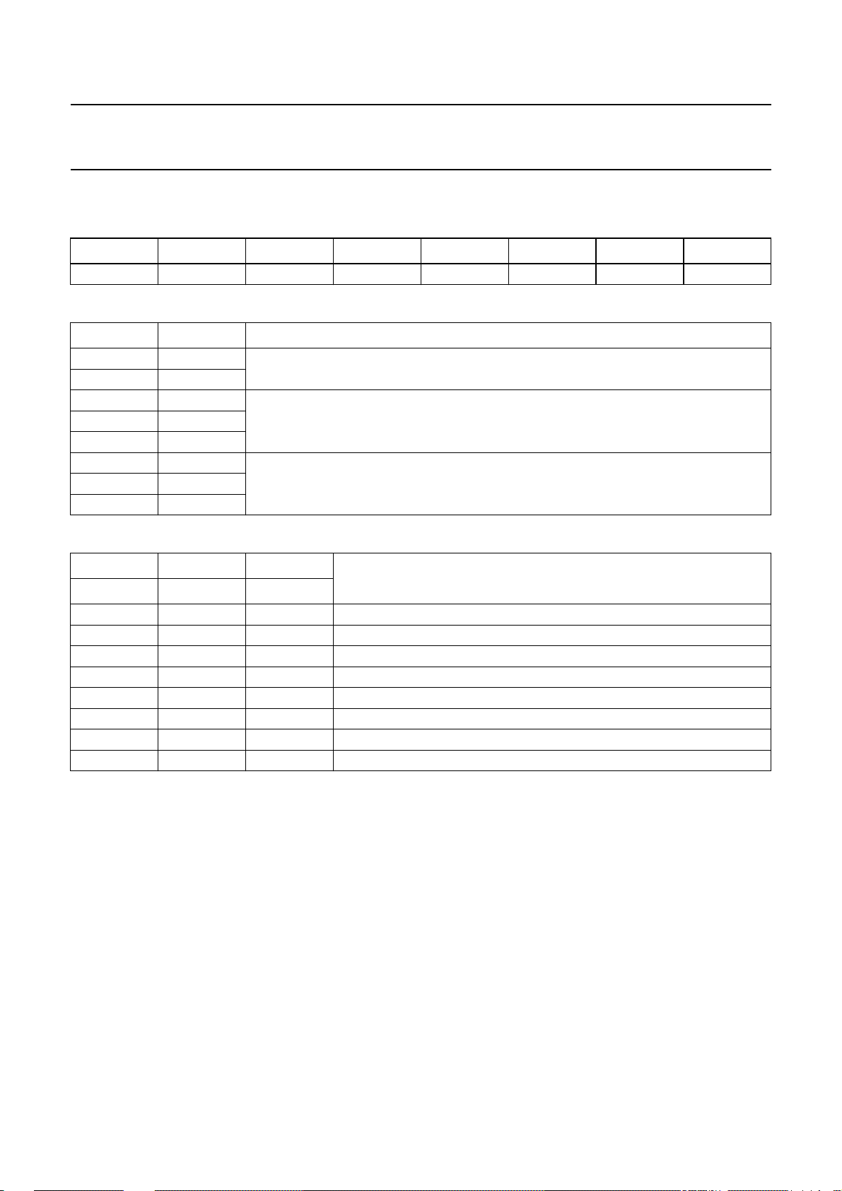
Philips Semiconductors Preliminary specification
Channel encoder/decoder CDR60 SAA7392
7.17.6 WOBBLE CONFIGURATION REGISTER 2(WOBBLECONFIG2)
Table 140 Wobble Configuration Register 2 (address 28H) - WRITE
76543210
−−PLLLBW.2 PLLLBW.1 PLLLBW.0 PLLHBW.2 PLLHBW.1 PLLHBW.0
Table 141 Description of WobbleConfig2 bits
BIT SYMBOL DESCRIPTION
7 − These 2 bits are reserved.
6 −
5 PLLLBW.2 These 3 bits select the PLL low-pass bandwidth; see Table 142.
4 PLLLBW.1
3 PLLLBW.0
2 PLLHBW.2 These 3 bits select the PLL high-pass bandwidth; see Table 142.
1 PLLHBW.1
0 PLLHBW.0
Table 142 Selection of the PLL high/low-pass bandwidth
PLLLBW.2 PLLLBW.1 PLLLBW.0
PLLHBW.2 PLLHBW.1 PLLHBW.0
0 0 0 43 kHz for 4.26 MHz system clock
0 0 1 21.5 kHz for 4.26 MHz system clock
0 1 0 10.7 kHz for 4.26 MHz system clock
0 1 1 5.4 kHz for 4.26 MHz system clock
1 0 0 2.7 kHz for 4.26 MHz system clock
1 0 1 1.35 kHz for 4.26 MHz system clock
1 1 0 670 Hz for 4.26 MHz system clock
1 1 1 350 Hz for 4.26 MHz system clock
HIGH/LOW-PASS BANDWIDTH
2000 Mar 21 61
Page 62
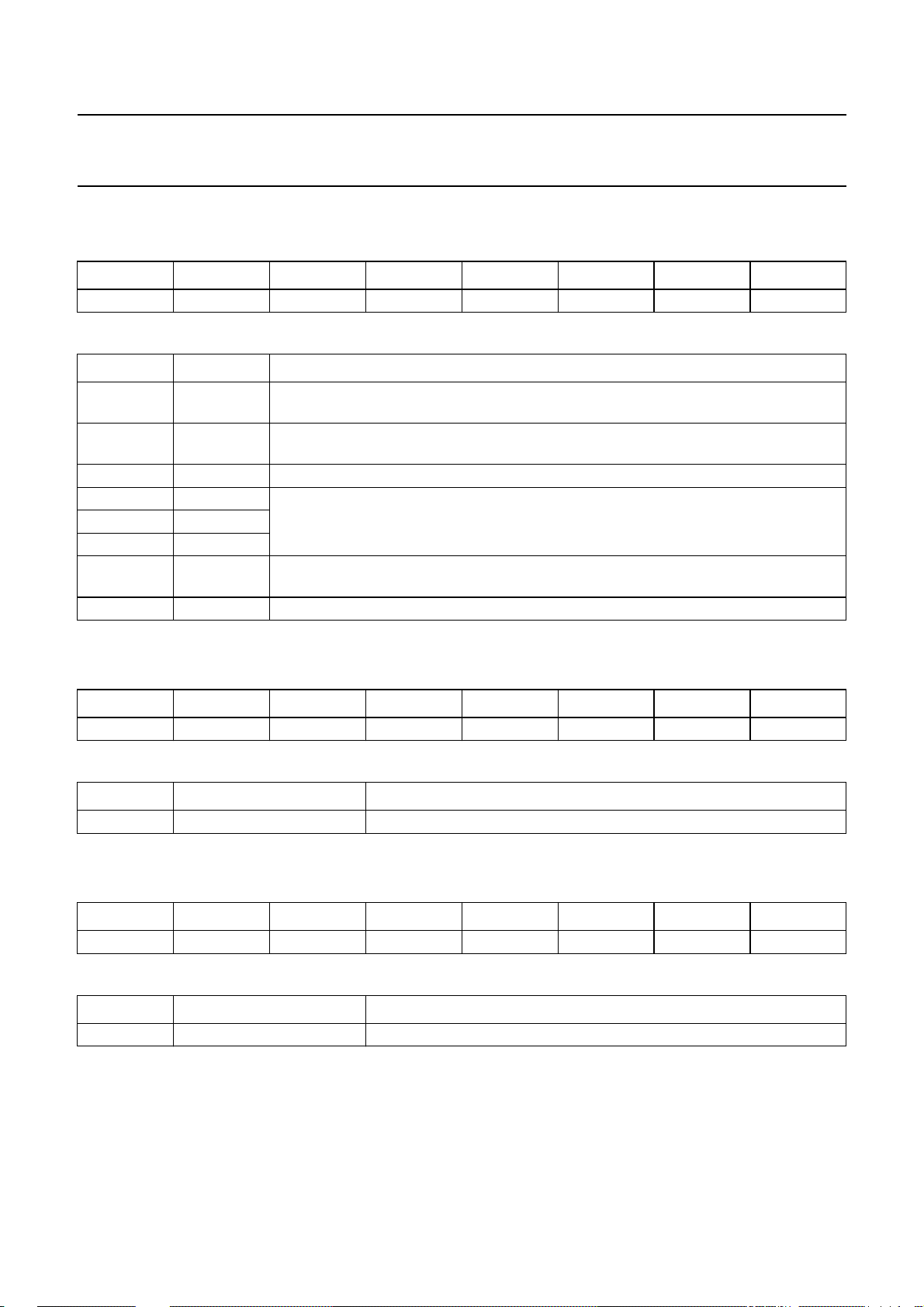
Philips Semiconductors Preliminary specification
Channel encoder/decoder CDR60 SAA7392
7.17.7 ATIP STATUS REGISTER (ATIPSTATUS)
Table 143 ATIP Status Register (address 29H) - READ
76543210
ATIPReady Busy CRCOK −−−SyncErr OIS
Table 144 Description of ATIPStatus bits
BIT SYMBOL DESCRIPTION
7 ATIPReady If ATIPReady = 0, then ATIP data isnot ready. If ATIPReady = 1, thenATIP datais ready
for read. Can also be an interrupt source.
6 Busy If Busy = 0, then ATIP data is not being read. If Busy = 1, then sub-CPU is busyreading
ATIP data.
5 CRCOK If CRCOK = 0, then CRC check is not OK. If CRCOK = 1, then CRC check is OK.
4 − These 3 bits are reserved.
3 −
2 −
1 SyncErr If SyncErr = 1, thendetected sync isnot in-phase withthe interpolated sync. Resync will
be done on next detected sync.
0 OIS If OIS = 1, then sync has been interpolated, no detected sync.
7.17.8 W
Table 145 Wobble Frequency Register 1 (address 2AH) - WRITE/READ
PLLFreq.15 PLLFreq.14 PLLFreq.13 PLLFreq.12 PLLFreq.11 PLLFreq.10 PLLFreq.9 PLLFreq.8
Table 146 Description of WobbleFreq1 bits
7.17.9 WOBBLE FREQUENCY REGISTER 2(WOBBLEFREQ2)
Table 147 Wobble Frequency Register 2 (address 2BH) - READ/WRITE
PLLFreq.7 PLLFreq.6 PLLFreq.5 PLLFreq.4 PLLFreq.3 PLLFreq.2 PLLFreq.1 PLLFreq.0
Table 148 Description of WobbleFreq2 bits
OBBLE FREQUENCY REGISTER 1(WOBBLEFREQ1)
76543210
BIT SYMBOL DESCRIPTION
7 to 0 PLLFreq<15:8> These 8 bits form the most significant byte of the PLL frequency.
76543210
BIT SYMBOL DESCRIPTION
7 to 0 PLLFreq<7:0> These 8 bits form the least significant byte of the PLL frequency.
2000 Mar 21 62
Page 63
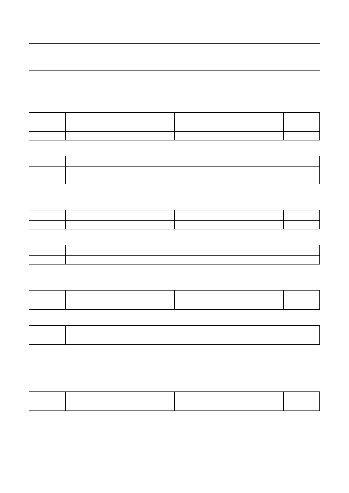
Philips Semiconductors Preliminary specification
Channel encoder/decoder CDR60 SAA7392
7.17.10 ATIP DATA REGISTER (ATIPDATA)
The upper 16 bits of the ATIP data can be obtained from this register by carrying out consecutive read operations.
Table 149 ATIP Data Register (address 2CH) - READ
76543210
ATIPData.23 ATIPData.22 ATIPData.21 ATIPData.20 ATIPData.19 ATIPData.18 ATIPData.17 ATIPData.16
ATIPData.15 ATIPData.14 ATIPData.13 ATIPData.12 ATIPData.11 ATIPData.10 ATIPData.9 ATIPData.8
Table 150 Description of ATIPData bits
BIT SYMBOL DESCRIPTION
7 to 0 ATIPData<23:16> most significant byte of ATIP data
7 to 0 ATIPData<15:8> penultimate byte of ATIP data
7.17.11 ATIP DATA END REGISTER (ATIPDATAEND)
Table 151 ATIP Data End Register (address 2DH) - READ
76543210
ATIPData.7 ATIPData.6 ATIPData.5 ATIPData.4 ATIPData.3 ATIPData.2 ATIPData.1 ATIPData.0
Table 152 Description of ATIPDataEnd bits
BIT SYMBOL DESCRIPTION
7 to 0 ATIPData<7:0> least significant byte of ATIP data
7.17.12 WOBBLE PEAK STATUS REGISTER (WOBBLESTATUS)
Table 153 Wobble Peak Status Register (address 2EH) - READ
76543210
WPPV.7 WPPV.6 WPPV.5 WPPV.4 WPPV.3 WPPV.2 WPPV.1 WPPV.0
Table 154 Description of WobbleStatus bits
BIT SYMBOL DESCRIPTION
7 to 0 WPPV<7:0> Peak value of the bit signal recovered by the Wobble processor.
7.17.13 ATIP ERROR REGISTER (ATER)
This register is an unbuffered counter and is incremented on every ATIP code CRC error. When the register reaches 255
it will hold and is reset by being read.
Table 155 ATIP Error Register (address 38H) - READ
76543210
ATER.7 ATER.6 ATER.5 ATER.4 ATER.3 ATER.2 ATER.1 ATER.0
2000 Mar 21 63
Page 64
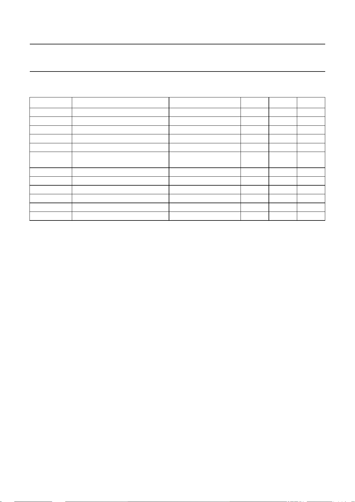
Philips Semiconductors Preliminary specification
Channel encoder/decoder CDR60 SAA7392
8 LIMITING VALUES
In accordance with the Absolute Maximum Rating System (IEC 60134).
SYMBOL PARAMETER CONDITIONS MIN. MAX. UNIT
V
V
V
V
V
∆V
I
O
I
IK
T
T
V
V
amb
stg
DDE
DDD
DDA
i(max)
O
DDD
es1
es2
supply voltage - pad output drivers notes 1 and 2 −0.5 +4.0 V
supply voltage - core/pad ring notes 1 and 2 −0.5 +4.0 V
supply voltage - analog notes 1 and 2 −0.5 +4.0 V
maximum input voltage (any input) −0.5 +5.0 V
output voltage (any output) −0.5 note 3 V
voltage difference between
V
and V
DDA
DDD
− 0.25 V
output current (continuous) − 20 mA
DC input diode current (continuous) − 20 mA
operating ambient temperature 0 +70 °C
storage temperature −55 +125 °C
electrostatic handling note 4 −1000 +1000 V
electrostatic handling note 5 −100 +100 V
Notes
1. All pad driver supply connections (V
) and analog and digital core/pad ring supply connections (V
DDE
must be made externally to the same power supply.
2. All VSS pins must be connected to the same external voltage.
3. (VDD+ 0.5) or 4.1 V depending on which one is lower.
4. Equivalent to discharging a 100 pF capacitor via a 1.5 kΩ series resistor with a rise time of 15 ns.
5. Equivalent to discharging a 200 pF capacitor via a 0.75 µH series inductor.
DDA
and V
DDD
)
2000 Mar 21 64
Page 65
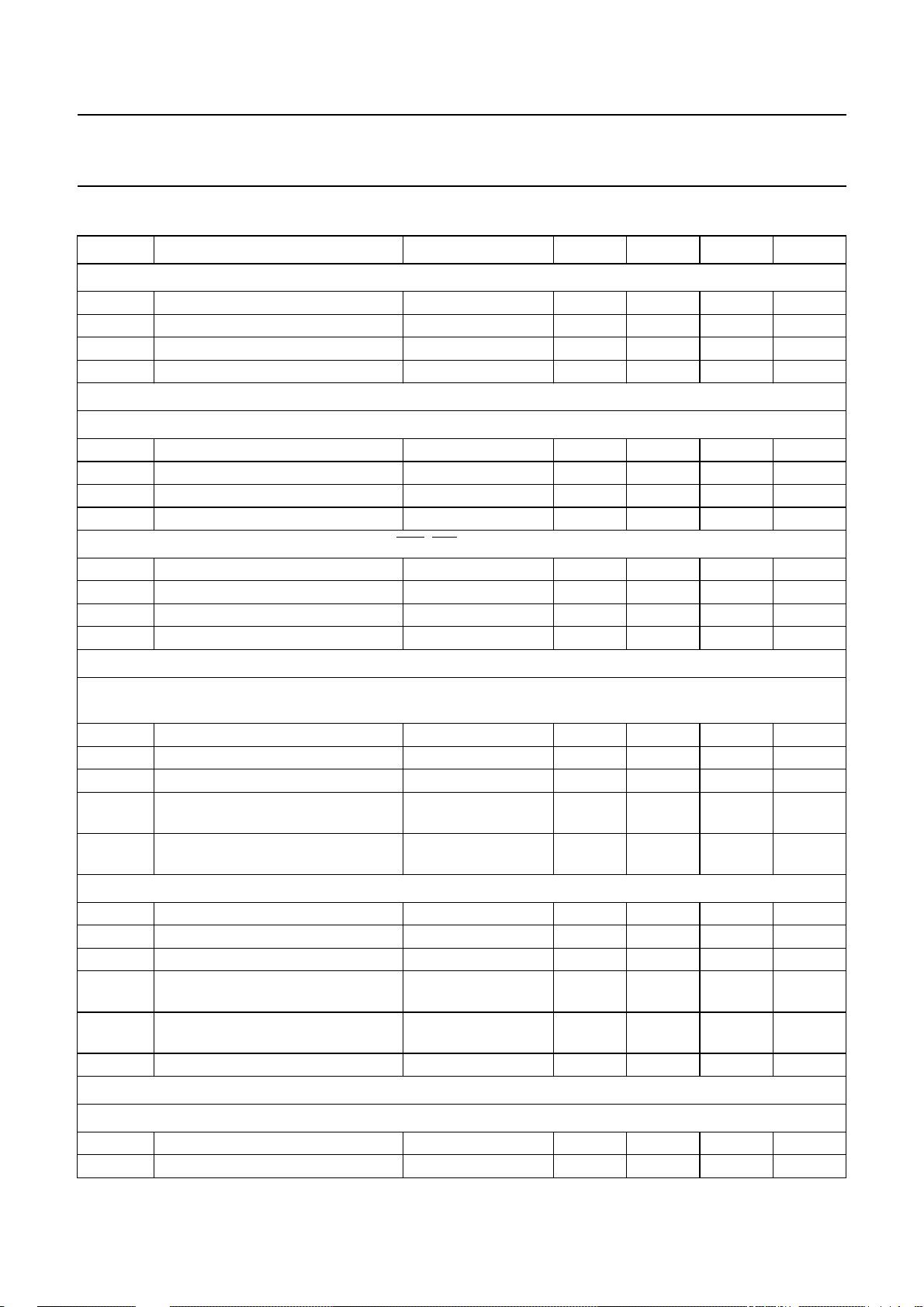
Philips Semiconductors Preliminary specification
Channel encoder/decoder CDR60 SAA7392
9 OPERATING CHARACTERISTICS
SYMBOL PARAMETER CONDITIONS MIN. TYP. MAX. UNIT
Supply
V
DDD
V
DDA
V
DDE
I
DD
Digital inputs
SCL (CMOS)
V
IL
V
IH
I
LI
C
i
TEST1, TEST2, OTD, MUXSWI, PANIC, PORE, WRI, RDI, ALE, CSI, PCAIN, DATAI, SUB, SFSY, T2 AND T1
V
IL
V
IH
I
LI
C
i
Digital outputs
supply voltage (core/pad ring) 3.0 3.3 3.6 V
supply voltage (analog) 3.0 3.3 3.6 V
supply voltage (pad output drivers) 3.0 3.3 3.6 V
supply current − 200 − mA
LOW-level input voltage −−0.3V
HIGH-level input voltage 0.7V
input leakage current Vi= 0 to V
DD
−10 − +10 µA
− 5.0 V
DD
DD
V
input capacitance −−10 pF
LOW-level input voltage −−0.8 V
HIGH-level input voltage 2.0 − 5.0 V
input leakage current Vi= 0 to V
DD
−10 − +10 µA
input capacitance −−10 pF
W441, ATPSYC, CL1, INT, STOPCK, V4, EBUOUT, SYNC, FLAG, DATAO, RCK, LASERON, XEFM, EFMDATA,
CFLG AND MEAS1
V
OL
V
OH
C
L
t
r
LOW-level output voltage IOL=4mA −−0.4 V
HIGH-level output voltage IOH= −4 mA 0.85V
−−V
DD
load capacitance −−20 pF
output rise time 0.4 to (VDD− 0.4);
−−20 ns
CL=20pF
t
f
output fall time (VDD− 0.4) to 0.4;
−−20 ns
CL=20pF
MOTO1 (3-STATE)
V
OL
V
OH
C
L
t
r
LOW-level output voltage IOL=4mA −−0.4 V
HIGH-level output voltage IOH= −4 mA 0.85V
−−V
DD
load capacitance −−20 pF
output rise time 0.4 to (VDD− 0.4);
−−20 ns
CL=20pF
t
f
output fall time (VDD− 0.4) to 0.4;
−−20 ns
CL=20pF
I
LI
3-state leakage current Vi= 0 to V
DD
−10 − +10 µA
Digital I/O
DA7 TO DA0, WCLK, BCLK AND MOTO2/T3
V
IL
V
IH
LOW-level input voltage −−0.3V
HIGH-level input voltage 0.7V
− 5.0 V
DD
DD
V
2000 Mar 21 65
Page 66
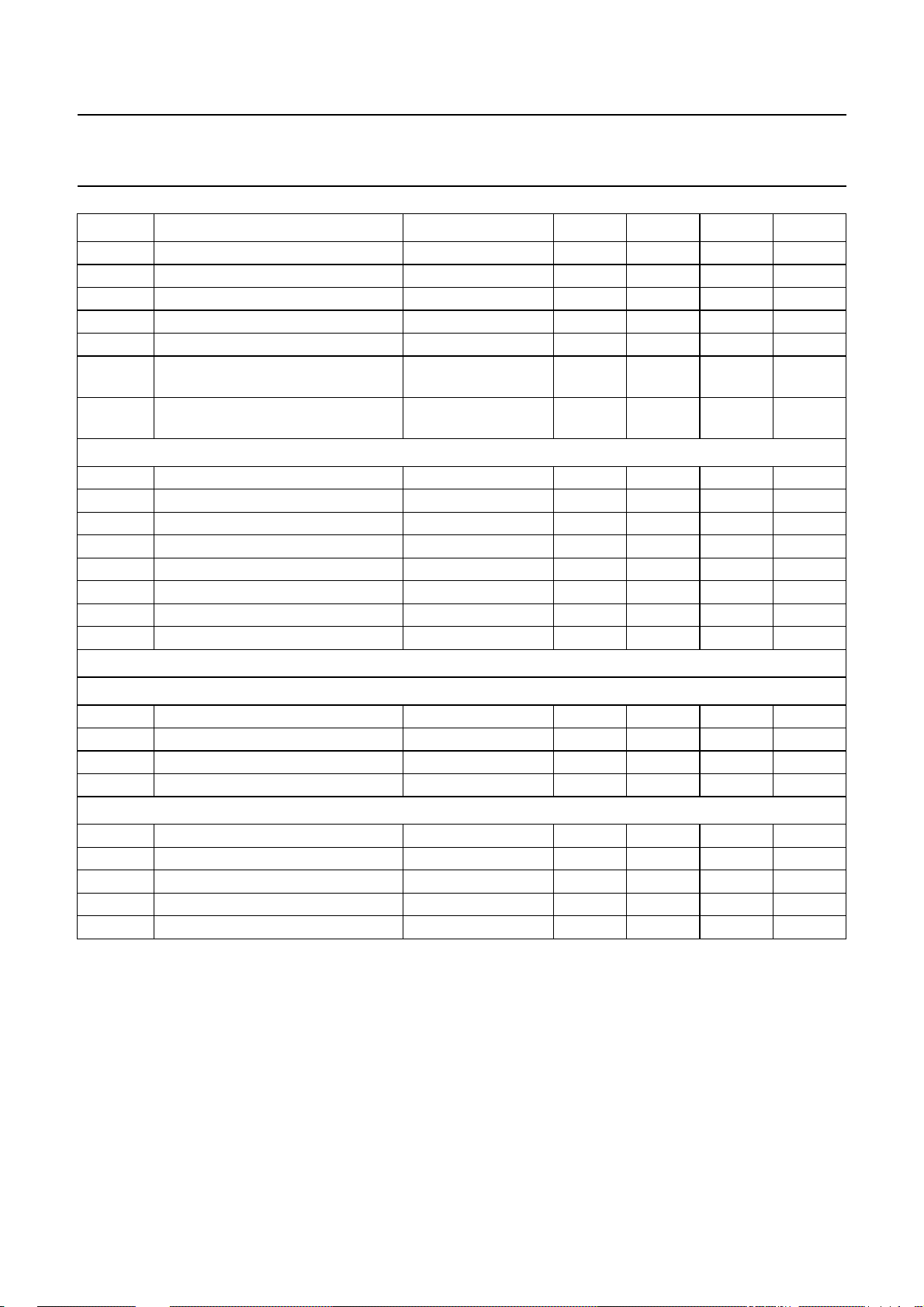
Philips Semiconductors Preliminary specification
Channel encoder/decoder CDR60 SAA7392
SYMBOL PARAMETER CONDITIONS MIN. TYP. MAX. UNIT
I
LI
C
i
V
OL
V
OH
C
L
t
r
t
f
SDA (I2C-BUS)
V
IL
V
IH
I
LI
C
i
V
OL
I
OL
C
L
t
f
Crystal oscillator
3-state leakage current Vi= 0 to V
DD
−10 − +10 µA
input capacitance −−10 pF
LOW-level output voltage IOL=4mA −−0.4 V
HIGH-level output voltage IOH= −4 mA 0.85V
−−V
DD
load capacitance −−20 pF
output rise time 0.4 to (VDD− 0.4);
−−20 ns
CL=20pF
output fall time (VDD− 0.4) to 0.4;
−−20 ns
CL=20pF
LOW-level input voltage −−0.3V
HIGH-level input voltage 0.7V
3-state leakage current Vi= 0 to V
DD
−10 − +10 µA
− 5.0 V
DD
DD
V
input capacitance −−10 pF
LOW-level output voltage IOL=4mA 0 − 0.4 V
LOW-level output current −−8mA
load capacitance −−20 pF
output fall time CL=20pF −−250 ns
XTLI (INPUT)
V
IL
V
IH
I
LI
C
i
LOW-level input voltage −−0.3V
HIGH-level input voltage 0.7V
input leakage current −10 − +10 µA
input capacitance −−−pF
XTLO (OUTPUT)
f
g
G
C
C
xtal
m
v
F
o
crystal frequency 4 8 − MHz
mutual conductance f = 100 kHz −−−mA/V
small signal voltage gain Gv= gm.R
feedback capacitance −−−pF
output capacitance −−−pF
V
DD
− 5.0 V
DD
O
−−−V/V
2000 Mar 21 66
Page 67
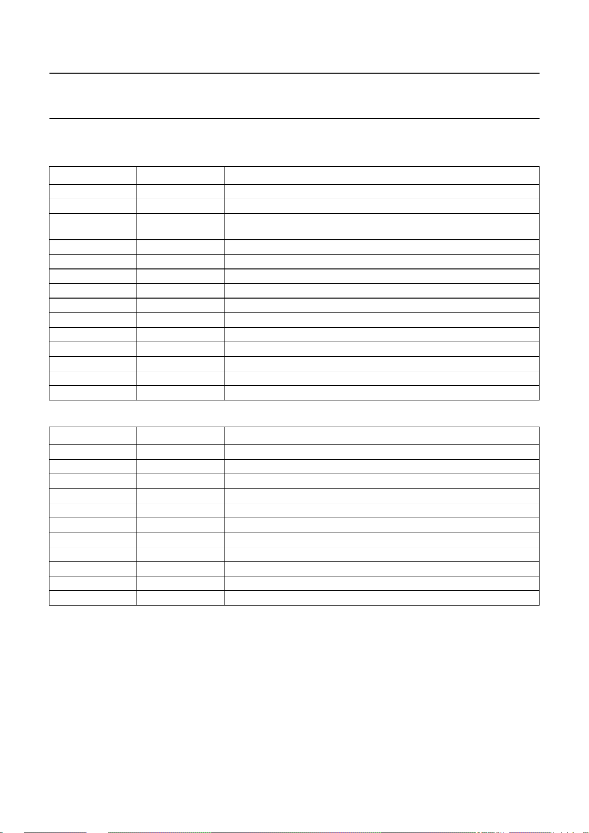
Philips Semiconductors Preliminary specification
Channel encoder/decoder CDR60 SAA7392
9.1 ADC and AGC parameters Table 156 ADC parameters
PARAMETER VALUE COMMENTS
Resolution 8-bit
Data format Simple Binary
Maximum sample
frequency
SINAD >26 dB 17.5 MHz signal − 12 dB down on ADC full scale, 70 MS/s sample rate
DNL −1.0/+1.0 LSB 70 MS/s; 1 MHz input
INL −2.0/+2.0 LSB 70 MS/s; 1 MHz input
Power dissipation <100 mW
Input range 1.47 − 2.91 V
Voltage reference 2.9 V top ladder reference
Bias current 100 µA provided externally
Bandwidth 35 MHz −3 dB (−0.5 effective bits)
Clock frequency 70 MHz defines sample rate
Clock duty cycle 40 to 60%
Clock jitter ±200 ps for 6.5-bit accuracy, f = 17.5 MHz
70 MS/s nominal rate 50 MS/s
Table 157 AGC parameters
PARAMETER VALUE COMMENTS
Output level 1.4 V(p-p)
Gain range −2.69 to +11.25 dB approx. linear in dBs
Gain step 1.1 dB
Bandwidth 35 MHz −3 dB point
Phase linearity 0.6 ns in bandwidth of 35 MHz
Resolution 5-bit
SNR 50 dB in bandwidth of 35 MHz
THD <−35 dB f = 17.5 MHz; V
Input range 0.39 to 1.96 V peak-to-peak value
Input impedance 7.57 kΩ nominal, at HIN
Offset voltage <30 mV
= 1.44 V; ADC load
out(p-p)
2000 Mar 21 67
Page 68

Philips Semiconductors Preliminary specification
Channel encoder/decoder CDR60 SAA7392
10 APPLICATION INFORMATION
10.1 Write start control of encoder in CD-ROM mode
In CD-ROM mode, the CDR60 is intended to operate in
lock-to-disc mode during write. When writing is stopped by
theEncode ControlBlock,the dataflow through thedevice
will also stop. All pointers will stop incrementing and the
BCLK clock ofthe I2S input interfacewill stop. As a result,
the buffer manager will stop outputting data to the CDR60.
Write start will be given while the encoder is in this ‘hot
stand-by’ state, with all pointers stopped and all clocks
stopped. It is extremely important to start the write from a
precisely definedinitial state. Hence, a ‘cold start’ must be
executed prior to the start of the write. This is as follows:
1. Start the CDR servo. Start the spindle motor servo in
‘tacho’ mode. Start focus and radial servo loops.
2. Program the Wobble processor to capture ATIP time
code data from the disc. (Lock-in the wobble PLL).
3. Jump to a suitable time prior to the ‘record start
address’. (e.g. 10 frames.)
4. Switch motor servo to ATIP signal. Allowenough time
for motor speed to stabilize before start of write. Use
motor monitor and wobble monitor functions for this.
5. Lock EFM PLL to crystal clock.
6. Program encoder in ‘CD, encode, flush mode’.
Program the EFM modulator to ‘WriteOn1,
WriteOn2 off’ mode. This is the reset state.
7. Reset the block encoder.
8. Program the encoder to ‘CD encode, normal mode’.
The encoder will fill itsinternal tables,but dataflow will
stop after a while, because no EFM data is output.
9. Program SubPresetCount and EFMPresetCount
registers.
10. Initialize the subcode insert block.
11. Read ATIP time again.
12. Start encoding after suitable delay by writing to
EncodeWriteControl. Turn on both WriteOn1 and
WriteOn2.
10.2 Write start control of encoder in Audio mode
In this mode the data flow is fixed speed as it is not
possible to stop the data stream from the ADC to the
CDR60. Because of this, a ‘hot start’ is needed.
1. Start the CDR servo. Start the spindle motor servo in
Tacho mode. Start focus and radial servo loops.
2. Program the Wobble processor to capture ATIP time
code from the disc. (Lock-in the wobble PLL).
3. Jump to a suitable time prior to the ‘record start
address’ (e.g. 10 frames).
4. Switch motor servo to ATIP signal. Allowenough time
for motor speed to stabilize before start of write. Use
motor monitor and wobble monitor functions for this.
5. Lock EFM PLL to I2S bit clock and FIFO filling.
6. Program encoder in ‘CD, encode, flush mode’.
Program EFM modulator to WriteOn1 off and
WriteOn2 on mode. Program input interface to digital
silence.
7. Program the encoder to ‘CD, encode, normal mode’.
The encoderwill start streaming digitalzero data. The
operationof PLLlocked toI2Sbit clockand FIFOfilling
will regulate the FIFO filling toward a nominal value.
8. Program SubPresetCount and EFMPresetCount
registers.
9. Initialize the subcode insert block.
10. Read ATIP time again.
11. Start encoding after suitable delay by writing to
EncodeWriteControl. Turn on WriteOn1.
10.3 Start-up of encode in flow-control operation
1. Reset the encoder. Switch LaserOn off, switch
WriteOn2 off and switch encoder to ‘flush’ mode.
2. Preset the device.
a) Preset the serial input format
b) Preset the subcode insertion block
c) Preset the EFM modulator block
d) Preset the EFM clock generator.
3. Let the disc runat thecorrect speed,let theEFM clock
generator produce the correct clock.
4. At this stage, the device is in Standby mode.
Everything is initialized, the encoder is still in ‘reset’
state and the I2S input clock is stopped. The encoder
cannot accept data because it is reset. Because flow
control is enabled the clock is stopped.
5. Initialize the block encoder pointers to point to the
correct data from where encoding should start.
6. Switch theencoder from ‘flush’ to ‘encodeplay’ mode.
At this point the encoder starts reading data from the
serialinterface butstops againafter a fewmilliseconds
because the its FIFO gets filled as the data out to the
EFM modulator is still blocked.
2000 Mar 21 68
Page 69

Philips Semiconductors Preliminary specification
Channel encoder/decoder CDR60 SAA7392
7. When the correct start address is found on the disc,
the LaserOn and WriteOn2 signals are switchedon at
the same time. As a result data flow in the encoder
starts while data is written to the disc.
10.4 Start-up of encoder in synchronous stream
mode
In synchronous stream mode operation is different
because the serial input stream cannot be gated off.
1. Reset the encoder. Switch LaserOn off, Switch
WriteOn2 off and switch encoder to ‘flush’ mode.
2. Preset the device.
a) Preset the serial input format
b) Preset the subcode insertion block
c) Preset the EFM modulator block
d) Preset the EFM clock generator. The EFM clock
generator must be programmed to slave to the
incoming serial stream.
3. Let the disc runat therequired speed. Make the motor
servo slave to the W441 wobble clock.
4. Switch on WriteOn2. This signal must be switched on
to allow data to leave the encoder when it enters it.
(Important to avoid overflow.)
5. At thisstage everything isinitialized. The inputstream
is running but doesnot enterthe encoder because it is
still in the ‘reset’ state. The output stream is running
too at the samespeed asthe input speed because the
EFM clock generator is setup like this.
6. The encoder is switched from ‘flush’ to ‘encode play’
mode. At this point the data stream starts. Data from
the serial in interface enters the encoder while data is
read out from it at approximately the same speed via
the EFM modulator. The FIFO will not overflow. The
data is discarded and not written to the disc because
LaserOn is still switch off.
7. When the correct start address is found on the disc
LaserOn is switched on allowing data stream to the
disc.
10.5 OperatingCDR60 in CAV mode, flow control on
input stream
For very high-speed operation it is possible to lock the
EFM clock to the ATIP wobble carrier. To do this W441
must be selected as the clock source while the position
erroris takenfrom XError. TheXError signalgives the time
difference between the ATIPSync and the QSync.
Programming the EFM clock generator like this with a
multiplicationfactor of 98will producean EFMclock thatis
synchronous with the ATIP carrier. It can be used to write
data in lock-to-disc mode.
10.6 Operating in CLV Mode, Flow Control on Input
Stream
Simply bypass the EFM PLL and use the system clock as
EFM source.
10.7 Operating in CLV Mode, Synchronous Stream
Operation
When an audio stream is input to the CDR60 encoder the
EFM clock mustlock tothe serialinput WCLKclock signal.
The position error is taken from the FIFOFill signal. This
will produce an EFM clock that is 98 times the WCLK
frequency.
2000 Mar 21 69
Page 70
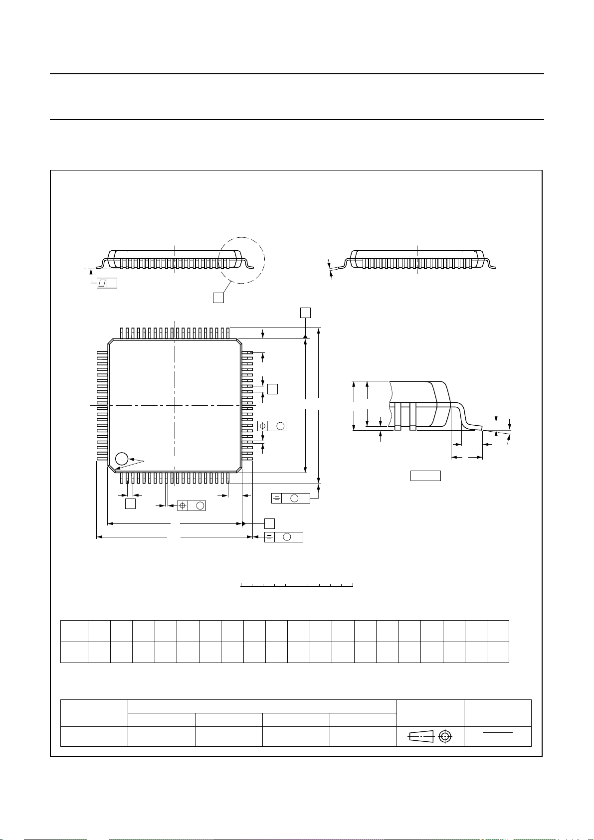
Philips Semiconductors Preliminary specification
Channel encoder/decoder CDR60 SAA7392
11 PACKAGE OUTLINE
LQFP80: plastic low profile quad flat package; 80 leads; body 12 x 12 x 1.4 mm
c
y
X
A
60 41
61
80
pin 1 index
1
Z
40
E
e
H
E
E
A
2
A
A
1
w M
b
p
21
20
detail X
SOT315-1
(A )
3
θ
L
p
L
Z
e
w M
b
p
D
D
H
D
v M
B
v M
0 5 10 mm
scale
DIMENSIONS (mm are the original dimensions)
UNIT
mm
A
A1A2A3b
max.
0.16
1.6
0.04
1.5
1.3
0.25
cE
p
0.27
0.18
0.13
0.12
(1)
(1) (1)(1)
D
12.1
11.9
eH
H
12.1
11.9
0.5
14.15
13.85
Note
1. Plastic or metal protrusions of 0.25 mm maximum per side are not included.
OUTLINE
VERSION
IEC JEDEC EIAJ
REFERENCES
SOT315-1 136E15 MS-026
2000 Mar 21 70
B
A
D
E
14.15
13.85
LL
p
0.75
0.30
0.15 0.10.21.0
EUROPEAN
PROJECTION
Z
1.45
1.05
D
Zywv θ
E
o
1.45
7
o
1.05
0
ISSUE DATE
99-12-27
00-01-19
Page 71

Philips Semiconductors Preliminary specification
Channel encoder/decoder CDR60 SAA7392
12 SOLDERING
12.1 Introduction to soldering surface mount packages
Thistext givesavery briefinsightto acomplextechnology.
A more in-depth account of soldering ICs can be found in
our
“Data Handbook IC26; Integrated Circuit Packages”
(document order number 9398 652 90011).
There is no soldering method that is ideal for all surface
mount IC packages. Wave soldering is not always suitable
for surface mount ICs, or for printed-circuit boards with
high population densities. In these situations reflow
soldering is often used.
12.2 Reflow soldering
Reflow soldering requires solder paste (a suspension of
fine solder particles, flux and binding agent) to be applied
tothe printed-circuitboard byscreenprinting, stencillingor
pressure-syringe dispensing before package placement.
Several methods exist for reflowing; for example,
infrared/convection heating in a conveyor type oven.
Throughput times (preheating, solderingand cooling)vary
between 100 and 200 seconds depending on heating
method.
Typical reflow peak temperatures range from
215 to 250 °C. The top-surface temperature of the
packages should preferable be kept below 230 °C.
12.3 Wave soldering
Conventional single wave soldering is not recommended
forsurface mountdevices (SMDs)or printed-circuit boards
with a high component density, as solder bridging and
non-wetting can present major problems.
To overcome these problems the double-wave soldering
method was specifically developed.
• Use a double-wave soldering method comprising a
turbulent wavewith high upward pressure followed by a
smooth laminar wave.
• For packages with leads on two sides and a pitch (e):
– larger than or equal to 1.27 mm, the footprint
longitudinal axis is preferred to be parallel to the
transport direction of the printed-circuit board;
– smaller than 1.27 mm, the footprint longitudinal axis
must be parallel to the transport direction of the
printed-circuit board.
The footprint must incorporate solder thieves at the
downstream end.
• Forpackages withleads onfour sides, thefootprint must
be placedat a 45° angleto the transport direction of the
printed-circuit board. The footprint must incorporate
solder thieves downstream and at the side corners.
During placement and beforesoldering, thepackage must
be fixed with a droplet of adhesive. The adhesive can be
applied by screen printing, pin transfer or syringe
dispensing. The package can be soldered after the
adhesive is cured.
Typical dwell time is 4 seconds at 250 °C.
A mildly-activated flux will eliminate the need for removal
of corrosive residues in most applications.
12.4 Manual soldering
Fix the component by first soldering two
diagonally-opposite end leads. Use a low voltage (24 V or
less) soldering iron applied to the flat part of the lead.
Contact time must be limited to 10 seconds at up to
300 °C.
When using a dedicated tool, all other leads can be
soldered in one operation within 2 to 5 seconds between
270 and 320 °C.
If wave soldering isused the following conditions must be
observed for optimal results:
2000 Mar 21 71
Page 72

Philips Semiconductors Preliminary specification
Channel encoder/decoder CDR60 SAA7392
12.5 Suitability of surface mount IC packages for wave and reflow soldering methods
PACKAGE
WAVE REFLOW
(1)
BGA, LFBGA, SQFP, TFBGA not suitable suitable
SOLDERING METHOD
HBCC, HLQFP, HSQFP, HSOP, HTQFP, HTSSOP, SMS not suitable
(3)
PLCC
, SO, SOJ suitable suitable
LQFP, QFP, TQFP not recommended
SSOP, TSSOP, VSO not recommended
(2)
(3)(4)
(5)
suitable
suitable
suitable
Notes
1. All surface mount (SMD) packages are moisture sensitive. Depending upon the moisture content, the maximum
temperature (with respect to time) and body size of the package, there is a risk that internal or external package
cracks may occur due to vaporization of the moisture in them (the so called popcorn effect). For details, refer to the
Drypack information in the
“Data Handbook IC26; Integrated Circuit Packages; Section: Packing Methods”
.
2. These packages arenot suitable for wave soldering as a solder joint between the printed-circuit board and heatsink
(at bottom version) can not be achieved, and as solder may stick to the heatsink (on top version).
3. If wave soldering is considered, then the package must be placed at a 45° angle to the solder wave direction.
The package footprint must incorporate solder thieves downstream and at the side corners.
4. Wave soldering is onlysuitable for LQFP, TQFP and QFP packages with a pitch (e) equal to or larger than 0.8 mm;
it is definitely not suitable for packages with a pitch (e) equal to or smaller than 0.65 mm.
5. Wave solderingis only suitable for SSOPand TSSOP packageswith a pitch (e) equalto or largerthan 0.65 mm; it is
definitely not suitable for packages with a pitch (e) equal to or smaller than 0.5 mm.
2000 Mar 21 72
Page 73
Philips Semiconductors Preliminary specification
Channel encoder/decoder CDR60 SAA7392
13 DEFINITIONS
Data sheet status
Objective specification This data sheet contains target or goal specifications for product development.
Preliminary specification This data sheet contains preliminary data; supplementary data may be published later.
Product specification This data sheet contains final product specifications.
Limiting values
Limiting values given are in accordance with the Absolute Maximum Rating System (IEC 134). Stress above one or
more of the limiting values may cause permanent damage to the device. These are stress ratings only and operation
of the device at these or at any other conditions above those given in the Characteristics sections of the specification
is not implied. Exposure to limiting values for extended periods may affect device reliability.
Application information
Where application information is given, it is advisory and does not form part of the specification.
14 LIFE SUPPORT APPLICATIONS
These products are not designed for use in life support appliances, devices, or systems where malfunction of these
products can reasonably be expected to result in personal injury. Philips customers using or selling these products for
use in suchapplications do so at their own risk and agree to fully indemnify Philips for any damages resulting from such
improper use or sale.
15 PURCHASE OF PHILIPS I
Purchase of Philips I
components inthe I2C systemprovided the systemconforms to theI2C specificationdefined by
Philips. This specification can be ordered using the code 9398 393 40011.
2
C COMPONENTS
2
C components conveys a license under the Philips’ I2C patent to use the
2000 Mar 21 73
Page 74

Philips Semiconductors Preliminary specification
Channel encoder/decoder CDR60 SAA7392
NOTES
2000 Mar 21 74
Page 75

Philips Semiconductors Preliminary specification
Channel encoder/decoder CDR60 SAA7392
NOTES
2000 Mar 21 75
Page 76

Philips Semiconductors – a w orldwide compan y
Argentina: see South America
Australia: 3 Figtree Drive, HOMEBUSH, NSW 2140,
Tel. +61 2 9704 8141, Fax. +61 2 9704 8139
Austria: Computerstr. 6, A-1101 WIEN, P.O. Box 213,
Tel. +43 1 60 101 1248, Fax. +43 1 60 101 1210
Belarus: Hotel Minsk Business Center, Bld. 3, r. 1211, Volodarski Str. 6,
220050 MINSK, Tel. +375 172 20 0733, Fax. +375 172 20 0773
Belgium: see The Netherlands
Brazil: see South America
Bulgaria: Philips Bulgaria Ltd., Energoproject, 15th floor,
51 James Bourchier Blvd., 1407 SOFIA,
Tel. +359 2 68 9211, Fax. +359 2 68 9102
Canada: PHILIPS SEMICONDUCTORS/COMPONENTS,
Tel. +1 800 234 7381, Fax. +1 800 943 0087
China/Hong Kong: 501 Hong Kong Industrial Technology Centre,
72 Tat Chee Avenue, Kowloon Tong, HONG KONG,
Tel. +852 2319 7888, Fax. +852 2319 7700
Colombia: see South America
Czech Republic: see Austria
Denmark: Sydhavnsgade 23, 1780 COPENHAGEN V,
Tel. +45 33 29 3333, Fax. +45 33 29 3905
Finland: Sinikalliontie 3, FIN-02630 ESPOO,
Tel. +358 9 615 800, Fax. +358 9 6158 0920
France: 51 Rue Carnot, BP317, 92156 SURESNES Cedex,
Tel. +33 1 4099 6161, Fax. +33 1 4099 6427
Germany: Hammerbrookstraße 69, D-20097 HAMBURG,
Tel. +49 40 2353 60, Fax. +49 40 2353 6300
Hungary: see Austria
India: Philips INDIA Ltd, Band Box Building, 2nd floor,
254-D, Dr. Annie Besant Road, Worli, MUMBAI 400 025,
Tel. +91 22 493 8541, Fax. +91 22 493 0966
Indonesia: PTPhilipsDevelopmentCorporation,Semiconductors Division,
Gedung Philips, Jl. Buncit Raya Kav.99-100, JAKARTA 12510,
Tel. +62 21 794 0040 ext. 2501, Fax. +62 21 794 0080
Ireland: Newstead, Clonskeagh, DUBLIN 14,
Tel. +353 1 7640 000, Fax. +353 1 7640 200
Israel: RAPAC Electronics, 7 Kehilat Saloniki St, PO Box 18053,
TEL AVIV 61180, Tel. +972 3 645 0444, Fax. +972 3 649 1007
Italy: PHILIPS SEMICONDUCTORS, ViaCasati, 23 - 20052MONZA (MI),
Tel. +39 039 203 6838, Fax +39 039 203 6800
Japan: Philips Bldg 13-37, Kohnan 2-chome, Minato-ku,
TOKYO 108-8507, Tel. +81 3 3740 5130, Fax. +81 3 3740 5057
Korea: Philips House, 260-199 Itaewon-dong, Yongsan-ku, SEOUL,
Tel. +82 2 709 1412, Fax. +82 2 709 1415
Malaysia: No. 76 Jalan Universiti, 46200 PETALING JAYA, SELANGOR,
Tel. +60 3 750 5214, Fax. +60 3 757 4880
Mexico: 5900 Gateway East, Suite 200, EL PASO, TEXAS 79905,
Tel. +9-5 800 234 7381, Fax +9-5 800 943 0087
Middle East: see Italy
Netherlands: Postbus 90050, 5600 PB EINDHOVEN, Bldg. VB,
Tel. +31 40 27 82785, Fax. +31 40 27 88399
New Zealand: 2 Wagener Place, C.P.O. Box 1041, AUCKLAND,
Tel. +64 9 849 4160, Fax. +64 9 849 7811
Norway: Box 1, Manglerud 0612, OSLO,
Tel. +47 22 74 8000, Fax. +47 22 74 8341
Pakistan: see Singapore
Philippines: Philips Semiconductors Philippines Inc.,
106 Valero St. Salcedo Village, P.O. Box 2108 MCC, MAKATI,
Metro MANILA, Tel. +63 2 816 6380, Fax. +63 2 817 3474
Poland: Al.Jerozolimskie 195 B, 02-222 WARSAW,
Tel. +48 22 5710 000, Fax. +48 22 5710 001
Portugal: see Spain
Romania: see Italy
Russia: Philips Russia, Ul. Usatcheva 35A, 119048 MOSCOW,
Tel. +7 095 755 6918, Fax. +7 095 755 6919
Singapore: Lorong 1, Toa Payoh, SINGAPORE 319762,
Tel. +65 350 2538, Fax. +65 251 6500
Slovakia: see Austria
Slovenia: see Italy
South Africa: S.A. PHILIPS Pty Ltd., 195-215 Main Road Martindale,
2092 JOHANNESBURG, P.O. Box 58088 Newville 2114,
Tel. +27 11 471 5401, Fax. +27 11 471 5398
South America: Al. Vicente Pinzon, 173, 6th floor,
04547-130 SÃO PAULO, SP, Brazil,
Tel. +55 11 821 2333, Fax. +55 11 821 2382
Spain: Balmes 22, 08007 BARCELONA,
Tel. +34 93 301 6312, Fax. +34 93 301 4107
Sweden: Kottbygatan 7, Akalla, S-16485 STOCKHOLM,
Tel. +46 8 5985 2000, Fax. +46 8 5985 2745
Switzerland: Allmendstrasse 140, CH-8027 ZÜRICH,
Tel. +41 1 488 2741 Fax. +41 1 488 3263
Taiwan: Philips Semiconductors, 6F, No. 96, Chien Kuo N. Rd., Sec. 1,
TAIPEI, Taiwan Tel. +886 2 2134 2886, Fax. +886 2 2134 2874
Thailand: PHILIPS ELECTRONICS (THAILAND) Ltd.,
209/2 Sanpavuth-Bangna Road Prakanong, BANGKOK 10260,
Tel. +66 2 745 4090, Fax. +66 2 398 0793
Turkey: Yukari Dudullu, Org. San. Blg., 2.Cad. Nr. 28 81260 Umraniye,
ISTANBUL, Tel. +90 216 522 1500, Fax. +90 216 522 1813
Ukraine: PHILIPS UKRAINE, 4 Patrice Lumumba str., Building B, Floor 7,
252042 KIEV, Tel. +380 44 264 2776, Fax. +380 44 268 0461
United Kingdom: Philips Semiconductors Ltd., 276 Bath Road, Hayes,
MIDDLESEX UB3 5BX, Tel. +44 208 730 5000, Fax. +44 208 754 8421
United States: 811 East Arques Avenue, SUNNYVALE, CA 94088-3409,
Tel. +1 800 234 7381, Fax. +1 800 943 0087
Uruguay: see South America
Vietnam: see Singapore
Yugoslavia: PHILIPS, Trg N. Pasica 5/v, 11000 BEOGRAD,
Tel. +381 11 3341 299, Fax.+381 11 3342 553
For all other countries apply to: Philips Semiconductors,
International Marketing & Sales Communications, Building BE-p, P.O. Box 218,
5600 MD EINDHOVEN, The Netherlands, Fax. +31 40 27 24825
© Philips Electronics N.V. SCA
All rights are reserved. Reproduction in whole or in part is prohibited without the prior written consent of the copyright owner.
The information presented in this document does not form part of any quotationor contract, is believed to be accurate and reliableand may be changed
without notice. No liability will be accepted by the publisher for any consequence of its use. Publication thereof does not convey nor imply any license
under patent- or other industrial or intellectual property rights.
2000
Internet: http://www.semiconductors.philips.com
69
Printed in The Netherlands 753503/01/pp76 Date of release: 2000 Mar 21 Document order number: 9397 750 04685
 Loading...