

Page 1

INTEGRATED CIRCUITS
DATA SH EET
SAA7390
High performance Compact
Disc-Recordable (CD-R) controller
Preliminary specification
File under Integrated Circuits, IC01
1996 Jul 02
Page 2

Philips Semiconductors Preliminary specification
High performance Compact
Disc-Recordable (CD-R) controller
CONTENTS
1 FEATURES
1.1 General
1.2 Interface logic (CD-ROM operation)
1.3 Hardware third-level error correction
1.4 Interface logic (CD-R operation)
1.5 DRAM buffer controller (256 kbytes × 8,
1 Mbyte × 8, 4 Mbytes × 8)
1.6 Additional product support
2 GENERAL DESCRIPTION
3 QUICK REFERENCE DATA
4 ORDERING INFORMATION
5 BLOCK DIAGRAM
6 PINNING
7 FUNCTIONAL DESCRIPTION
7.1 Input clock doubler
7.2 Block encoder
7.3 Front-end
7.4 Track descriptor block
7.5 Buffer manager
8 MICROCONTROLLER INTERFACE
8.1 Microprocessor interface status register
8.2 Microcontroller interface command register
8.3 Microprocessor interrupts
8.4 Microcontroller RAM organization
9 FRONT PANEL AND MISCELLANEOUS
CONTROL SIGNALS
9.1 S2B UART registers
9.2 SPI UART registers
9.3 Track Descriptor Block (TDB) generation
9.4 Miscellaneous control registers
10 FRONT-END
10.1 Minute-second frame addressing and header
information
10.2 Front-end status and control
11 BUFFER MANAGER
SAA7390
11.1 Front-end to buffer manager interface
11.2 Microcontroller to buffer manager interface
11.3 ECC to buffer manager interface
11.4 SCSI to buffer manager interface
11.5 Miscellaneous buffer manager considerations
11.6 Host interface related registers
11.7 CDB2 related registers
12 FRAME BUFFER ORGANIZATION
13 SUMMARY OF CONTROL REGISTER MAP
14 LIMITING VALUES
15 OPERATING CHARACTERISTICS
15.1 I2S-bus timing; data mode
15.2 EIAJ timing; audio mode
15.3 R-W timing (see Fig.17)
15.4 C-flag timing (see Fig.18)
15.5 S2B interface timing
15.6 SPI interface timing
15.7 Microprocessor interface
15.8 Host interface
15.9 DRAM interface (the SAA7390 is designed to
operate with standard 70 ns DRAMs)
16 PACKAGE OUTLINE
17 SOLDERING
17.1 Introduction
17.2 Reflow soldering
17.3 Wave soldering
17.4 Repairing soldered joints
18 DEFINITIONS
19 LIFE SUPPORT APPLICATIONS
1996 Jul 02 2
Page 3

Philips Semiconductors Preliminary specification
High performance Compact
Disc-Recordable (CD-R) controller
1 FEATURES
1.1 General
• 8× speed CD-ROM, 4× speed Compact
Disc-Recordable (CD-R) controller
• 16.9 Mbytes/s burst rate to host controller
• High performance CD-ROM and CD-R interface logic
• 128 pin QFP package.
1.2 Interface logic (CD-ROM operation)
• Full 8× speed hardware operation
• Block decoder
• Sector sequencer
• CRC checking of Mode 1 and Mode 2, Form 1 sectors
• 212 ms watch-dog timer
• Sub-code interface with synchronization
• C-flag interface for absolute time stamp.
1.3 Hardware third-level error correction
• Third-level correction provides superior performance in
unfavourable conditions
• Full hardware error correction to reduce microcontroller
overhead
• Corrections are automatically written to the DRAM
frame buffer.
1.4 Interface logic (CD-R operation)
• Block encoder (using a modified CDB2).
1.5 DRAM buffer controller (256 kbytes × 8,
1 Mbyte × 8, 4 Mbytes × 8)
• DRAM buffer manager
• Ten level arbitration logic
• Utilizes low cost 70 ns DRAMs
• Page mode DRAM access for high-speed error
correction and host interface data transfers
• Data organization by 3 kbytes frames.
1.6 Additional product support
SAA7390
• Dedicated Serial Peripheral Interface (SPI)
• Third level error correction and encoding
• 80C32 microcontroller interface
• 53CF90 or 53CF92A/B fast SCSI processor interface
(may also use ATAPI processor).
2 GENERAL DESCRIPTION
The SAA7390 is a high integration ASIC that incorporates
all of the logic necessary to connect a CD-60 based
decoder to a SCSI or ATAPI host. It also supports a data
path from the host to the CDCEP (compact disc encoder)
for CD-R applications. An 80C32 microcontroller and a
53CF94/92A (or an ATAPI interface device) are required
to provide the full block encode/decode functions. The
following functions are supported:
• Input clock doubler
• Block encoder (using a modified CDB2)
• Block decoder
• CRC checking of Mode 1 and Mode 2, Form 1 sectors
• Red book audio pass through to SCSI or ATAPI
• Sub-code and Q-channel support
• Dedicated S2B interface UART
• Dedicated SPI interface UART
• Up to 4 Mbytes DRAM buffer manager
• Third-level error correction and encoding
• Automatic storage of audio and data
• 80C32 microcontroller interface
• 53CF90 or 53CF92A/B fast SCSI or Wapiti ATAPI
processor interface.
The SAA7390 uses a 33.8688 MHz clock and is capable
of accepting data at eight times (n = 8 or 1.4 Mbytes/s) the
normal CD-ROM data rate. The minimum host burst rate
capability of the SAA7390 is 5 Mbytes/s.
Third level error correction hardware is included to
improve the correction efficiency of the system. The buffer
manager hardware utilizes a ten-level arbitration unit and
can stop the clock to the static microcontroller to emulate
a wait condition when necessary. The host interface is
capable of burst rates to 16.9 Mbytes/s.
• Input clock doubler
• All control registers mapped into 80C32 special function
memory space
• Red book audio pass through to host interface
• Sub-code and Q-channel support
1996 Jul 02 3
Page 4

Philips Semiconductors Preliminary specification
High performance Compact
SAA7390
Disc-Recordable (CD-R) controller
The SAA7390 comprises four major functional blocks:
• The front-end block connects to the external CD-60
based decoder and fully processes the incoming data
stream
• The buffer manager block provides the address
generation and timing control for the external DRAMs
• The ECC block performs the error correction functions in
hardware on the data stored in the DRAM buffer.
• The block encoder function (realized via a modified
CDB2) serializes the data from the buffer, appends the
sync pattern, header, sub-header, third level ECC parity
and EDC bytes as necessary, performs the required
scrambling and outputs them to the CDCEP using a
special data clock (98 clock cycles per word selection
period).
3 QUICK REFERENCE DATA
SYMBOL PARAMETER MIN. TYP. MAX. UNIT
V
DD
T
amb
T
stg
digital supply voltage 4.5 5.0 5.5 V
operating ambient temperature 0 − 70 °C
storage temperature −55 − +150 °C
4 ORDERING INFORMATION
TYPE
NUMBER
SAA7390GP
Note
1. This device uses a Symbios logic package.
(1)
NAME DESCRIPTION VERSION
SQFP128 plastic quad flat package; 128 leads (lead length 1.6 mm);
body 14 × 20 × 2.8 mm
PACKAGE
SOT387-2
1996 Jul 02 4
Page 5

Philips Semiconductors Preliminary specification
High performance Compact
Disc-Recordable (CD-R) controller
5 BLOCK DIAGRAM
handbook, full pagewidth
data subcode
CD
DECODER
BASIC
ENGINE
DATA
CONVERTER
AND SUB-CODE
UART
data
subcode
C-flag
WRITE I/F
LAYERED
CORRECTOR
SAA7390
BUFFER MANAGER
ERROR
256K × 8 to 4M × 8
DRAM BUFFER
ENCODE
MICROCONTROLLER INTERFACE
BUFFER
MAPPER
SPI UART
GENERIC
EXTERNAL
INTERFACE
S2B UART
SAA7390
SCSI
or
ATAPI
interface
S2B
interface
MGE518
80C32 MICROCONTROLLER
128K × 8 ROM
SPI
interface
Fig.1 Block diagram (simplified).
6 PINNING
All input and bidirectional signals are TTL level with Schmitt-trigger logic, with the exception of OSCIN. All output
signals are TTL levels unless otherwise stated. (PD = internal pull-down; PU = internal pull-up).
SYMBOL PIN I/O TYPE DESCRIPTION
DA0 1 O DRAM address bus; bit DA0
DA1 2 O DRAM address bus; bit DA1
DA2 3 O DRAM address bus; bit DA2
V
SS1
4 − ground 1
DA3 5 O DRAM address bus; bit DA3
DA4 6 O DRAM address bus; bit DA4
DA5 7 O DRAM address bus; bit DA5
V
SS2
8 − ground 2
DA6 9 O DRAM address bus; bit DA6
1996 Jul 02 5
Page 6

Philips Semiconductors Preliminary specification
High performance Compact
SAA7390
Disc-Recordable (CD-R) controller
SYMBOL PIN I/O TYPE DESCRIPTION
DA7 10 O DRAM address bus; bit DA7
V
DD1
DA8 12 O DRAM address bus; bit DA8
DA9 13 O DRAM address bus; bit DA9
DA10 14 O DRAM address bus; bit DA10
RAS 15 O DRAM row address section; active LOW
CAS 16 O DRAM column address selection; active LOW
DWR 17 O DRAM write; active LOW
DOE 18 O DRAM output enable; active LOW
DD0 19 I/O PD DRAM data bus; bit DD0
V
DD2
DD1 21 I/O PD DRAM data bus; bit DD1
DD2 22 I/O PD DRAM data bus; bit DD2
DD3 23 I/O PD DRAM data bus; bit DD3
DD4 24 I/O PD DRAM data bus; bit DD4
V
SS3
DD5 26 I/O PD DRAM data bus; bit DD5
DD6 27 I/O PD DRAM data bus; bit DD6
DD7 28 I/O PD DRAM data bus; bit DD7
COM_IN 29 I serial data in from basic engine
COM_OUT 30 O serial data out to basic engine
COM_CLK 31 O serial data clock
COM_ACK 32 I serial data acknowledge
TRAYSW 33 I PU active LOW when tray is in
EJECT 34 I PU opens tray; active LOW
LQDATA 35 O latched qualified data
LWCLK 36 O latched word clock
V
DD3
LED 38 O CMOS; 24 mA panel LED; active LOW; open drain; 24 mA (min.) sink capability
V
SS4
SCLK 40 O audio data clock
V
SS5
SYSRES 42 O system reset; active HIGH
SYSRES 43 O system reset; active LOW
V
DD4
GPIO3 45 I/O PD general purpose input/output 3
GPIO4 46 I/O PD general purpose input/output 4
VOLUP 47 I PU volume up; active LOW
VOLDN 48 I PU volume down; active LOW
UC_AD0 49 I/O microprocessor multiplexed address/data bus; bit UC_AD0
UC_AD1 50 I/O microprocessor multiplexed address/data bus; bit UC_AD1
11 − power supply 1
20 − power supply 2
25 − ground 3
37 − power supply 3
39 − ground 4
41 − ground 5
44 − power supply 4
1996 Jul 02 6
Page 7

Philips Semiconductors Preliminary specification
High performance Compact
SAA7390
Disc-Recordable (CD-R) controller
SYMBOL PIN I/O TYPE DESCRIPTION
UC_AD2 51 I/O microprocessor multiplexed address/data bus; bit UC_AD2
UC_AD3 52 I/O microprocessor multiplexed address/data bus; bit UC_AD3
V
SS6
UC_AD4 54 I/O microprocessor multiplexed address/data bus; bit UC_AD4
UC_AD5 55 I/O microprocessor multiplexed address/data bus; bit UC_AD5
UC_AD6 56 I/O microprocessor multiplexed address/data bus; bit UC_AD6
UC_AD7 57 I/O microprocessor multiplexed address/data bus; bit UC_AD7
V
DD5
UC_LA0 59 O latched lower address; bit UC_LA0
UC_LA1 60 O latched lower address; bit UC_LA1
UC_LA2 61 O latched lower address; bit UC_LA2
V
SS7
UC_LA3 63 O latched lower address; bit UC_LA3
UC_LA4 64 O latched lower address; bit UC_LA4
UC_LA5 65 O latched lower address; bit UC_LA5
UC_LA6 66 O latched lower address; bit UC_LA6
UC_LA7 67 O latched lower address; bit UC_LA7
V
SS8
PCLK 69 O 33.8688 MHz microprocessor clock
V
DD6
ALE 71 I address latch enable
UC_WR 72 I write enable
UC_RD 73 I read enable
INT 74 O CMOS interrupt to microcontroller; active LOW; open drain
UC_A8 75 I upper address; bit UC_A8
UC_A9 76 I upper address; bit UC_A9
UC_A10 77 I upper address; bit UC_A10
SYS_SYNC 78 I system synchronization from basic engine
UC_A11 79 I upper address; bit UC_A11
UC_A12 80 I upper address; bit UC_A12
UC_A13 81 I upper address; bit UC_A13
COM_SYNC 82 I communication synchronization from basic engine
UC_A14 83 I upper address; bit UC_A14
UC_A15 84 I upper address; bit UC_A15
SD0 85 I/O internal data bus; bit SD0
V
DD6
SD1 87 I/O internal data bus; bit SD1
SD2 88 I/O internal data bus; bit SD2
V
SS9
SD3 90 I/O internal data bus; bit SD3
SD4 91 I/O internal data bus; bit SD4
53 − ground 6
58 − power supply 5
62 − ground 7
68 − ground 8
70 − power supply 6
86 − power supply 6
89 − ground 9
1996 Jul 02 7
Page 8

Philips Semiconductors Preliminary specification
High performance Compact
SAA7390
Disc-Recordable (CD-R) controller
SYMBOL PIN I/O TYPE DESCRIPTION
SD5 92 I/O internal data bus; bit SD5
SD6 93 I/O internal data bus; bit SD6
SD7 94 I/O internal data bus; bit SD7
V
SS10
DREQ 96 I PD DMA request
DACK 97 O DMA acknowledge; active LOW
HOSTRD 98 O read enable; active LOW
HOSTWR 99 O write enable; active LOW
HOSTSEL 100 O chip select; active LOW
CSAB 101 I word strobe for write data
CCLAB 102 I clock for write data
CDAAB 103 O write data stream
RXS2B 104 I PU receive data
TXS2B 105 O transmit data
CPR 106 O ready to accept data; active LOW
SCSIRST 107 I reset from SCSI bus; active LOW
POR 108 I power-on reset; active LOW
TCL_GPIO1 109 I/O PD general purpose input/output 1 (also used as test-mode clock)
SPR 110 I ready to send data; active LOW
TDA_GPIO2 111 I/O PD general purpose input/output 2 (also used as test-mode data)
HFD 112 I laser on and focused status; active LOW
KILL 113 I PU mute audio; active LOW
V
SS11
MCOUT 115 O motor control output from PWM
MCIN 116 I PD motor control input from decoder
RXSUB 117 I PU sub-code input
CFLAG 118 I PU C1 and C2 status
V
SS12
OSCIN 120 I input clock from decoder
V
DD7
CLAB 122 I clock input
DAAB 123 I data input
WSAB 124 I word strobe input
EFAB 125 I error flags
V
SS13
CLK34 127 O 33.8688 MHz output clock
V
DD8
95 − ground 10
114 − ground 11
119 − ground 12
121 − power supply 7
126 − ground 13
128 − power supply 8
1996 Jul 02 8
Page 9

Philips Semiconductors Preliminary specification
High performance Compact
Disc-Recordable (CD-R) controller
handbook, full pagewidth
CDAAB
RXS2B
TXS2B
CPR
SCSIRST
POR
TCL_GPIO1
SPR
TDA_GPIO2
HFD
KILL
V
SS11
MCOUT
MCIN
RXSUB
CFLAG
V
SS12
OSCIN
V
DD7
CLAB
DAAB
WSAB
EFAB
V
SS13
CLK34
V
DD8
103
104
105
106
107
108
109
110
111
112
113
114
115
116
117
118
119
120
121
122
123
124
125
126
127
128
CCLAB
CSAB
HOSTSEL
HOSTWR
9998979695949392919089888786858483828180797877767574737271706968676665
102
101
100
432
1
SS1
DA0
DA1
DA2
V
HOSTRD
DACK
6
5
DA3
DA4
DREQ
7
DA5
V
8
V
SS10
SS2
SD7
9
DA6
SD6
10
DA7
V
SD5
11
DD1
SD4
12
DA8
SD3
13
DA9
V
14
DA10
SS9
SD2
15
RAS
SD1
16
CAS
DD6
V
SD0
SAA7390
18
17
DWR
DOE
UC_A15
UC_A14
20
19
DD0VDD2
UC_A12
COM_SYNC
UC_A13
23
22
21
DD1
DD2
DD3
UC_A11
SYS_SYNC
25
24
SS3
DD4
V
UC_A10
UC_A9
27
26
DD5
DD6
UC_A8
28
DD7
INT
UC_RD
30
29
COM_IN
COM_OUT
UC_WR
ALE
32
31
COM_CLK
COM_ACK
DD6
V
PCLK
34
33
EJECT
TRAYSW
SS8
V
UC_LA7
36
35
LWCLK
LQDATA
SAA7390
UC_LA6
UC_LA5
64
UC_LA4
63
UC_LA3
V
62
SS7
61
UC_LA2
60
UC_LA1
59
UC_LA0
V
58
DD5
UC_AD7
57
56
UC_AD6
UC_AD5
55
54
UC_AD4
V
53
SS6
52
UC_AD3
51
UC_AD2
50
UC_AD1
49
UC_AD0
48
VOLDN
47
VOLUP
46
GPIO4
45
GPIO3
V
44
DD4
SYSRES
43
42
SYSRES
V
41
40
SCLK
V
39
38
37
MGE517
LED
DD3
V
SS5
SS4
Fig.2 Pin configuration.
1996 Jul 02 9
Page 10

Philips Semiconductors Preliminary specification
High performance Compact
Disc-Recordable (CD-R) controller
left
output
AUDIO
TDA8425
PROCESSOR
RAM
output
DAC
AND
CD-ROM
ENCODER
right
TDA1545A
SAA7390
DECODER
ATAPI
interface
WAPITI
53CF90
SCSI-2
interface
53CF92A
53CF92B
ATAPI/SCSI
INTERFACE
80C32
MICRO
CD-ROM
SAA7390
MGE519
book, full pagewidth
DISC
COMPACT
DISC MOTOR
LO9465
DECODER
CDR650
S83C752
CONTROLLER
L2465
CD LOADER
DISC
COMPACT
ENCODER
SIGNAL
PROCESSOR
TDA1371
TDA1372
MICRO
SERVO
SERVO
DIGITAL
CONTROLLER
SERVO
DIGITAL
DRIVERS
CDM24
3-BEAM
MECHANISM
OQ8845
OQ8844
Fig.3 Double-speed write quad-speed play CD-R system D65420 with ATAPI or SCSI-2 interface.
1996 Jul 02 10
Page 11

Philips Semiconductors Preliminary specification
High performance Compact
Disc-Recordable (CD-R) controller
7 FUNCTIONAL DESCRIPTION
7.1 Input clock doubler
To facilitate compatibility of the SAA7390 with all of the
available CD decoders, a clock doubler has been included.
This clock doubler may take a 16.9344 MHz clock and
double this when requested to do so by the
microcontroller. Logic has been included to remove the
possibility of a ‘runt’ clock pulse when the doubler is
engaged. Once engaged, the only way to disengage it is
via a reset condition.
7.2 Block encoder
To support the write function, a modified version of the
CDB2 function has been included. The block encoder
accepts parallel data from the buffer manager, serializes it,
calculates the CRC and third-level ECC parity bytes and
appends them when and where necessary. The RAM
required during the parity calculation is included on the
SAA7390.
The following modifications to the CDB2 have been made:
• Word select in bypass mode has been inverted to match
the data mode
• The ‘end-of-frame’ signal is now generated during the
bypass and CD-ROM mode and will interrupt the
microcontroller at the end of each frame
• The ‘end-of-frame’ signal is also used to correctly
synchronize between bypass mode and regular data
mode at the end of a frame. The modes programmed
into the CDB2 command, header, sub-header and block
size registers will automatically switch in or out at the
end of frame
• DRQ in CCMD is also synchronized to frame boundaries
using the ‘end-of-frame’ signal. This change is valid for
both bypass and regular data modes.
7.3 Front-end
The front-end section of the SAA7390 is identical to the
front-end of the mini-SEQUOIA (also found on the
SAA7385), with the exception of the Serial Peripheral
Interface (SPI). The front-end is comprised of many
sub-sections.
7.3.1 B
The block decoder first reverses the bits of each received
byte and then runs them through a linear feedback shift
register to be de-scrambled. The polynomial used to
de-scramble the serial data is as follows: X
LOCK DECODER
15
+X+1
SAA7390
It also detects and tests the synchronization field and will
start the data clock when commanded. The de-scrambled
header is assembled into four registers with header ready
and header error status (see HDRRDY and HDRERR in
RDDSTAT). The data clock does not have to be enabled
to receive valid headers.
Also included in this section is the logic required to decide
when to automatically start collecting data and sub-code
information based on the contents of the Q-channel
registers.
7.3.2 S
The sector sequencer de-serializes the data and error
flags from the block decoder and determines when to:
• Write data to the buffer
• Write flags to the buffer
• Test the header to determine the Mode
• Test the sub-header to determine the Form
• Test the CRC
• End the sector and write the status byte to the buffer.
Included in the sector sequencer is the CRC generator
which checks each Yellow book or Green book sector as it
is shifted into the SAA7390 in accordance with the
following polynomial:
32+X31+X16+X15+X4+X3
X
The status of each sector is saved and written to the buffer
at the end of the sector.
7.3.3 S
A UART which samples asynchronous bits on a 24 clocks
per bit basis is included. This is required because the
CD-60 based decoders output the sub-code data at
nominally 24 clocks per bit, but not synchronized to the
data. Also included is a sub-code synchronization detector
which senses the beginning of each new sector of
sub-code information. The serial sub-code information is
assembled into bytes in the following order:
Data bits 7 to 0 = 0, Q, R, S, T, U, V and W.
As each byte is assembled, it is sent to the buffer manager
to be written to the DRAM buffer. At the same time, the
Q-channel bits are assembled into bytes and sent to the
buffer. All Q-channel bytes except CRC are sorted in
registers for use by the microcontroller. The Q-channel
CRC (last two bytes) is checked just before the end of the
sub-code sector. If the CRC check fails, BADQ in
RDDSTAT is available to the microcontroller and is written
into the buffer at the end of the sector.
ECTOR SEQUENCER
+X+1
UB-CODE RECEIVE AND Q-CHANNEL EXTRACTOR
1996 Jul 02 11
Page 12

Philips Semiconductors Preliminary specification
High performance Compact
Disc-Recordable (CD-R) controller
When the ten Q-channel registers have been updated,
QFRMRDY in RDDSTAT is set. The ten Q-channel
registers are valid while QFRMRDY is set. In the audio
mode, HDRRDY in RDDSTAT generates this interrupt, but
the QFRMRDY bit will still be available as status to the
microcontroller.
7.3.4 C-
The C-flag bits, or corrector flags, are also 24 data clocks
long and reception of these bits is achieved using the
same method as for the sub-code; in this event, the C-flag
data is synchronized to the data.
The difference is that only one bit is used; F1, the absolute
time synchronization information. When in audio mode
and ENABRED in FECTL is set, receipt of F1 set will start
the internal data clock after the next rising edge of word
strobe (WSAB) which is the left channel sample when the
CD-60 decoder is programmed for EIAJ audio format.
When in audio mode, the Q-channel information provides
the MSF address and the F1 flag provides the start of
frame information; together these provide an absolute byte
address on the disc.
7.3.5 S2B UART
This UART is provided for communication with a second
slave microcontroller. It is hard-wired for one start-bit, eight
data bits, a parity bit and one stop bit. Parity testing can be
programmed to be either odd parity or even parity. Parity
error and over-run status are provided via PE and
OVRRUN in S2BSTAT. Selectable baud rates of
31.25, 62.5 and 187.5 kbaud are available via S2BSEL1
and S2BSEL0 in BRGSEL. Once the start-bit is found, the
data sampling time does not adapt dynamically, therefore
parity errors may occur depending on the baud rate
selected.
FLAG RECEIVER
SAA7390
7.3.6 SPI UART
This UART is provided for communication with a second
slave microcontroller used in Philips CD-R engines.
7.3.7 W
A pair of counters are included which output a 967 µs reset
pulse to the entire chip and the SYSRES and SYSRES
pins if the timer is not reset during the 212 ms time-out
period. The watch-dog timer is reset by setting RWMD in
FECTL HIGH then LOW. If RWMD is left HIGH, the
watch-dog function is disabled.
7.3.8 G
The final block of logic in the front-end consists of:
a programmable, linear pulse-width modulator for
spindle-motor control; an address de-multiplexer for the
address/data bus of the microcontroller; plus audio
multiplexing and muting circuitry for full control of Red
book audio data to an external Digital-to-Analog Converter
(DAC).
7.4 Track descriptor block
Logic has been included to simplify the creation of the
track descriptor block. This is achieved by allowing one
frame to be repeated a selectable number of times. Once
this repeated pattern is complete, the normal data is then
sent to the front-end.
ATCH-DOG TIMER
LUE LOGIC (GLIC)
1996 Jul 02 12
Page 13

Philips Semiconductors Preliminary specification
High performance Compact
Disc-Recordable (CD-R) controller
7.5 Buffer manager
The buffer manager provides the arbitration for the
different processes that wish to access the DRAM buffer.
These processes include the front-end, microcontroller
requests, CDB2 accesses, ECC accesses, host interface
requests and DRAM refreshing.
To manage a DRAM interface with up to four devices
requesting access to the DRAM, the following priority
scheme is used. The DRAM control logic will start an
access on the next rising edge of the clock after a request
is received. If two or more requests are pending then the
priority is:
1. Front-end (highest priority)
2. A refresh cycle (required every 15.6 µs) granted
priority for one access
3. Microcontroller requests
4. Host interface requests
5. ECC requests (lowest priority).
SAA7390
A burst access by ECC or host interface will only be
interrupted by a higher priority access request.
In addition to the priority logic, logic is required for the
front-end sources of data. The priority is; CDB2 requests
(highest) frame data, flag data, sub-code data, Q-channel
data and finally status byte. All front-end sources are
granted priority over the host interface logic, ECC, refresh
and data will be written into the frame store during the next
cycle. However, the microcontroller has priority over the
lower three front-end sources and will be granted an
access after front-end frame data or flag data is written to
memory.
The required timing (see Figs 4 to 11) operate with the
industry standard 70 ns DRAMs. The interface is designed
to operate with 256 kbytes, 1 Mbyte, and 4 Mbytes of
DRAM. A single byte access cycles requires five clock
cycles of 29.5 ns each, totalling 147.5 ns.
handbook, full pagewidth
CLOCK
RAS
CAS
ADDRESS ROW COL
DATA
DOE
Fig.4 Byte mode single access read cycle.
1996 Jul 02 13
latch data
MGE392
Page 14

Philips Semiconductors Preliminary specification
High performance Compact
Disc-Recordable (CD-R) controller
handbook, full pagewidth
CLOCK
RAS
CAS
ADDRESS
DATA
WRITE
ROW COL
SAA7390
DATA
MGE393
handbook, full pagewidth
CLOCK
ADDRESS ROW COL1 COL2 COL3 COL4
DATA
Fig.5 Byte mode single access write cycle.
RAS
CAS
latch latch latch
DOE
MGE394
Fig.6 ECC burst access read cycle.
1996 Jul 02 14
Page 15

Philips Semiconductors Preliminary specification
High performance Compact
Disc-Recordable (CD-R) controller
handbook, full pagewidth
CLOCK
RAS
CAS
ADDRESS ROW COL1 COL2 COL3 COL4
DATA
WRITE
DATA1 DATA2 DATA3 DATA4
SAA7390
MGE395
handbook, full pagewidth
CLOCK
RAS
CAS
ADDRESS ROW COL1 COL2 COL3 COL4
DATA
DOE
Fig.7 ECC burst access write cycle.
latch data latch data latch data
MGE396
Fig.8 Host interface fast burst access read cycle (2 clocks).
1996 Jul 02 15
Page 16

Philips Semiconductors Preliminary specification
High performance Compact
Disc-Recordable (CD-R) controller
handbook, full pagewidth
CLOCK
RAS
CAS
ADDRESS ROW COL1 COL2 COL3 COL4
DATA
WRITE
DATA1 DATA2 DATA3 DATA4
SAA7390
MGE397
handbook, full pagewidth
CLOCK
QA
QB
QC
RAS
CAS
ADDRESS ROW COL1 COL2 COL3 COL4
DATA
DOE
Fig.9 Host interface fast burst access write cycle (2 clocks).
latch data latch data latch data
MGE520
Fig.10 Host interface standard burst access read cycle (3 clocks).
1996 Jul 02 16
Page 17

Philips Semiconductors Preliminary specification
High performance Compact
Disc-Recordable (CD-R) controller
handbook, full pagewidth
CLOCK
QA
QB
QC
RAS
CAS
ADDRESS ROW COL1 COL2 COL3 COL4
DATA
WRITE
DATA1 DATA2 DATA3 DATA4
SAA7390
MGE521
Fig.11 Host interface standard burst access write cycle (3 clocks).
8 MICROCONTROLLER INTERFACE
8.1 Microprocessor interface status register
Table 1 NUM_COR register: 0xF08E; note 1
DATA BYTE
MNEMONIC R/W
76543210
NUM_COR R NUM_COR7 to NUM_COR0
Note
1. Register 0xF08E indicates the number of corrections performed during the most recently executed
CORRECT_P_SYNDROMES or CORRECT_Q_SYNDROMES command. Note that NUM_COR is only valid after
completion of the CORRECT_P_SYNDROMES or CORRECT_Q_SYNDROMES command, and becomes invalid
upon execution of any other command.
Table 2 ECC_STATUS register: 0xF086; note 1
DATA BYTE
MNEMONIC R/W
765 4 3 2 1 0
ECCSTAT R −−−FLG_EQ0 CRC_EQ0 PS_EQ0 QS_EQ0 ECC_ACT
Note
1. Register 0xF086 provides status information on the current or last ECC command.
1996 Jul 02 17
Page 18

Philips Semiconductors Preliminary specification
High performance Compact
SAA7390
Disc-Recordable (CD-R) controller
Table 3 ECCSTAT definitions
MNEMONIC DESCRIPTION
ECC_ACT asserted while a command other than ASSERT_ABORT or RELEASE_ABORT remains active
QS_EQ0 asserted when all Q syndromes are zero
PS_EQ0 asserted when all P syndromes are zero
CRC_EQ0 asserted when the CRC remainder calculated by the CRC_CALCULATE command is all zeros
FLG_EQ0 asserted when all flag bytes in ECC RAM are zero
8.2 Microcontroller interface command register
Table 4 ECCCTL register: 0xF085; note 1
MNEMONIC R/W
76543210
ECCCTL R/W −−−−ECC_COMMAND3 to ECC_COMMAND0
Note
1. The ECC_COMMAND definitions are explained in Table 5.
DATA BYTE
Table 5 Definitions of ECC_COMMAND3 to ECC_COMMAND0
EEC_COMMAND DESCRIPTION
0000 ASSERT_ABORT
0001 RELEASE_ABORT
0010 CALCULATE_SYNDROMES (not Mode 2, Form 1)
0011 CALCULATE_SYNDROMES (Mode 2, Form 1)
0100 CRC_RECALCULATE (not Mode 2, Form 1)
0101 CRC_RECALCULATE (Mode 2, Form 1)
0110 COPY_RESULTS (not Mode 2, Form 1)
0111 COPY_RESULTS (Mode 2, Form 1)
1000 CORRECT_P_SYNDROMES
1001 CORRECT_Q_SYNDROMES
1100 TEST_ECC_ROM
1101 TEST_ECC_RAM_READ
1110 TEST_ECC_RAM_WRITE
Table 6 Command descriptions
COMMAND DESCRIPTION
ASSERT_ABORT Terminates any currently active operation and re-initializes the ECC logic. Remains in
reset state until occurrence of the RELEASE_ABORT command. At power-on reset,
the ECC is in the ASSERT_ABORT state. All microprocessor status bits are reset
when the ECC is in the ASSERT_ABORT state.
RELEASE_ABORT Terminates the ASSERT_ABORT command and enables activation of other
commands.
1996 Jul 02 18
Page 19

Philips Semiconductors Preliminary specification
High performance Compact
SAA7390
Disc-Recordable (CD-R) controller
COMMAND DESCRIPTION
CRC_RECALCULATE Calculate CRC remainder buffer data, storing result in ECC RAM and updating
microprocessor status bit CRC_EQ0. Mode 2, Form 1 uses address 16 : 2075, or
0 : 2067; note 1
CALCULATE_SYNDROMESPrepares buffer for correction, calculates P and Q syndromes, and copies error flags
and CRC remainder from buffer to ECC RAM. The microprocessor status bits
PS_EQ0, QS_EQ0 and FLAGS_EQ0 are updated at the end of this operation.
1. Copy header from buffer to ECC RAM (Mode 2, Form 1 only)
2. Write to the buffer.
Not Mode 2, Form 1:
Address 0 → 0x00; Address1:10→0xFF; Address 11 → 0x00;
Address 2068 : 2075 → 0x00
Mode 2, Form 1:
Address 0 → 0x00; Address1:10→0xFF; Address 11 : 15 → 0x00
3. Read header and frame data from buffer to calculate P and Q syndromes
psyn[0 : 85].s1, psyn[0 : 85].s0, qsyn[0 : 51].s1 and qsyn[0 : 51].s0, storing results
in ECC RAM
4. Copy error flags from buffer to ECC RAM
5. Copy CRC remainder from buffer to ECC RAM
6. Update microprocessor status bits PS_EQ0, QS_EQ0 and FLAGS_EQ0.
COPY_RESULTS
Copies current ECC RAM contents to the buffer memory:
1. Copy header flags from ECC RAM to buffer (Mode 2, Form 1 only)
2. Copy error Flags from ECC RAM to buffer
3. Copy CRC remainder from ECC RAM to buffer
4. Copy P syndromes from ECC RAM to buffer
5. Copy Q syndromes from ECC RAM to buffer.
CORRECT_P_SYNDROMESScan all P syndromes and perform P-syndrome calculation. The microprocessor status
bits PS_EQ0, QS_EQ0 and FLAGS_EQ0 are updated at the end of this operation.
CORRECT_Q_SYNDROMESScan all Q syndromes and perform Q-syndrome calculation. The microprocessor
status bits PS_EQ0, QS_EQ0 and FLAGS_EQ0 are updated at the end of this
operation.
TEST_ECC_ROM Read each exponent and log in the alpha ROM to the NUM_COR register. This
command may only be terminated by the ASSERT_ABORT command.
TEST_ECC_RAM_READ Read ECC RAM addresses 0 : 591 and copy to buffer addresses 0 : 591.
TEST_ECC_RAM_WRITE Read buffer addresses 0 : 591 and copy to ECC RAM addresses 0 : 591.
Note
1. 16 : 2075 and 0 : 2067 are address frame offsets. The frame buffer organization is shown in Table 76.
1996 Jul 02 19
Page 20

Philips Semiconductors Preliminary specification
High performance Compact
SAA7390
Disc-Recordable (CD-R) controller
8.3 Microprocessor interrupts
An interrupts pulse is generated upon completion of any of the following commands:
• CALCULATE_SYNDROMES (not Mode 2, Form 1)
• CALCULATE_SYNDROMES (Mode 2, Form 1)
• CRC_RECALCULATE (not Mode 2, Form 1)
• CRC_RECALCULATE (Mode 2, Form 1)
• COPY_RESULTS (not Mode 2, Form 1)
• COPY_RESULTS (Mode 2, Form 1)
• CORRECT_P_SYNDROMES
• CORRECT_Q_SYNDROMES
• TEST_ECC_ROM
• TEST_ECC_RAM_READ
• TEST_ECC_RAM_WRITE.
If a command is aborted by the ASSERT_ABORT command, a spurious interrupt may be generated within five clock
cycles of the ASSERT_ABORT command.
Table 7 Command execution times; note 1
COMMAND CYCLES
CALCULATE_SYNDROMES (not Mode 2, Form 1) 5604 186.8 2658
CALCULATE_SYNDROMES (Mode 2, Form 1) 5600 186.7 2654
CRC_RECALCULATE (not Mode 2, Form 1) 4136 137.9 2068
CRC_RECALCULATE (Mode 2, Form 1) 4120 137.3 2060
COPY_RESULTS (not Mode 2, Form 1) 1148 38.3 574
COPY_RESULTS (Mode 2, Form 1) 1156 38.5 578
CORRECT_P_SYNDROMES
(maximum addition per correction)
CORRECT_Q_SYNDROMES
(maximum addition per correction)
TEST_ECC_RAM_READ 1184 39.5 592
TEST_ECC_RAM_WRITE 1184 39.5 592
Note
1. All times indicated reflect two clock cycles per memory access for all accesses other than P and Q corrections.
P and Q corrections reflect seven clock cycles per memory access. Execution times will be extended due to refresh
timing, other buffer traffic, and configuration of nibble-wide memory.
8.3.1 I
NTERRUPT REGISTER DEFINITIONS
1466
157
888
167
TIME (µs)
at 33 MHz
48.9
5.2
29.6
5.6
MEMORY
ACCESSES
0
2
0
2
Two registers are used to control the operation of the interrupt logic. The register INTRMSK allows each interrupt to be
enabled or disabled. INTRMSK and INTRFLG are cleared on reset to initially disable and clear all interrupts; the output
latch controlling the INT line is set on a reset; this must be cleared by writing 0x00 to INTRFLG. To enable an interrupt,
the bit that corresponds to the interrupt in INTRFLG must be set. The INTRFLG register shows the status of the
interrupts. If any bit is HIGH then an interrupt has occurred since the last time the bit was cleared. Writing a zero to any
1996 Jul 02 20
Page 21

Philips Semiconductors Preliminary specification
High performance Compact
SAA7390
Disc-Recordable (CD-R) controller
bit location in INTRFLG will clear the corresponding interrupt. If a masked interrupt occurs, the microcontroller can still
detect the occurrence because the event is still posted in INTRFLG.
Table 8 Interrupt mask register: 0xF0FB
MNEMONIC R/W
76543210
INTRMSK R/W MASK7 MASK6 MASK5 MASK4 MASK3 MASK2 MASK1 MASK0
Each bit in register 0xF0FB corresponds to the interrupt at the same bit location in register 0xF0FC. To enable an
interrupt, the bit in this register must be set HIGH.
Table 9 Interrupt flag register: F0FC; note 1
MNEMONIC R/W
765 43210
INTRFLG R/W CDB2INT FETXINT FERXINT ECC_COR FE_HDR FE2352 STR_LST FRM_STR
Note
1. If any bit is set in this register an interrupt is sent to the microcontroller. Table 10 shows when the interrupts are
asserted; assuming the corresponding mask bit is set.
DATA BYTE
DATA BYTE
Table 10 INTRFLG field descriptions
FIELD DESCRIPTION
FRM_STR set one when one complete frame is stored
STR_LST set at the start of the last frame
FE_2352 set if the front-end data exceeds 2352 bytes
FE_HDR front-end interrupt for header (or Q channel) ready
ECC_COR ECC interrupt for correction complete
RFERXINT front-end interrupt for receive ready
FETXINT front-end interrupt for transmit ready
CDB2INT CDB2 interrupts: see CSTAT (Table 78) for bit descriptions
8.4 Microcontroller RAM organization
MICFRM# is used to determine the frame address for the
microcontroller access through the frame window
0x8000 to 0x8FFF. To obtain the actual byte location
within the buffer RAM, the lower 12 bits of the
microcontroller address form the relative offset and hence
the absolute address is found.
Note that the microcontroller has the option of addressing
memory in a linear fashion using the 32 kbytes address
space between 0x000 and 0x7FFF. If this 32 kbytes page
is used, the PAGEREG must be programmed with the
required page address. PAGEREG is used to select the
required page when the microcontroller makes a linear
access to the buffer memory using the address space
0x7000 to 0x7FFF. The actual address is the fifteen LSBs
from the microcontroller plus 32768 times the value in
PAGEREG.
1996 Jul 02 21
Page 22

Philips Semiconductors Preliminary specification
High performance Compact
SAA7390
Disc-Recordable (CD-R) controller
Table 11 Microcontroller frame number address registers: 0xF0F6 and 0xF0F7; note 1
MNEMONIC R/W
76543210
MICFRM# R/W FRAME7 FRAME6 FRAME5 FRAME4 FRAME3 FRAME2 FRAME1 FRAME0
MICFRM# R/W −−−−−FRAME10 FRAME9 FRAME8
Note
1. Registers 0xF0F6 and 0xF0F7 provide the frame number address for the microcontroller access to memory. The
counter associated with these registers is loaded after the most significant byte is written; the least significant byte
must be written first to ensure that the counter is loaded correctly. If a DRAM access is in progress that uses the
address from the counter, the update will be delayed until the access is complete.
Table 12 Microcontroller address page register: 0xF0FF; note 1
MNEMONIC R/W
76 5 43210
PAGEREG R/W − MA_21 MA_20 MA_19 MA_18 MA_17 MA_16 MA_15
Note
1. Register 0xF0FF is used by the buffer manager for the upper address lines when the microcontroller addresses
non-frame memory. These registers overlap frame memory, so register 0xF0FF must be programmed with an
address in the top part of the memory if no overlap is required. The microcontroller page address line is selected from
this register. The outputs are used directly to control DRAM access cycles, and will affect any current DRAM cycle
in progress.
DATA BYTE
DATA BYTE
It is possible to access three contiguous frames from the
microcontroller by reading the three data sector windows,
0x8000 to 0x8FFF, 0x9000 to 0x9FFF and
0xA000 to 0xAFFF. This function is required for the
decoding of the sub-code information. If the ‘next’ frame
wraps past the last frame pointer (LASTFRM) then the
pointers are modified to wrap back to the start pointer
onwards (FEFRM#); this section is transparent to the
microcontroller.
1996 Jul 02 22
Page 23

Philips Semiconductors Preliminary specification
High performance Compact
Disc-Recordable (CD-R) controller
handbook, halfpage
0000
SCRATCH PAD RAM
7FFF
8000
DATA SECTOR WINDOW
9000
DATA SECTOR WINDOW
A000
DATA SECTOR WINDOW
AFFF
SAA7390
80C32
(FRAME 0)
(FRAME 1)
(FRAME 2)
F000
FFFF
SAA7390
CONTROL REGISTERS
MGE522
Fig.12 Address map for the microcontroller.
Table 13 SAA7390 address map details for the 80C32
ADDRESS FUNCTION
0000 to 7FFF This 32 kbytes window is used to address and portion the DRAM buffer. It is intended for non-frame
mapped memory to be addressed through this window. The upper page address bits (to address the
full range of the DRAM buffer) are set by the linear address page register (PAGEREG).
8000 to 8FFF All accesses to frame memory use this window to read or write to the buffer memory. The actual
address to the DRAM buffer is Micro Frame Number (MICFRM#) times 3 k plus the 12 LSBs from the
80C32.
9000 to 9FFF This frame window is identical to the frame 0 window with the exception that one is added to the
value from the Micro Frame Number (MICFRM#).
A000-AFFF This frame window is identical to the frame 0 window with the exception that two is added to the
value from the Micro Frame Number (MICFRM#).
B000-EFFF Not used; output 3-state.
F000-FFFF SAA7390 control registers.
1996 Jul 02 23
Page 24
Philips Semiconductors Preliminary specification
High performance Compact
SAA7390
Disc-Recordable (CD-R) controller
9 FRONT PANEL AND MISCELLANEOUS CONTROL SIGNALS
This Chapter describes the various SAA7390 control signals; front panel and basic engine signals, jumper settings and
use of the general purpose signals.
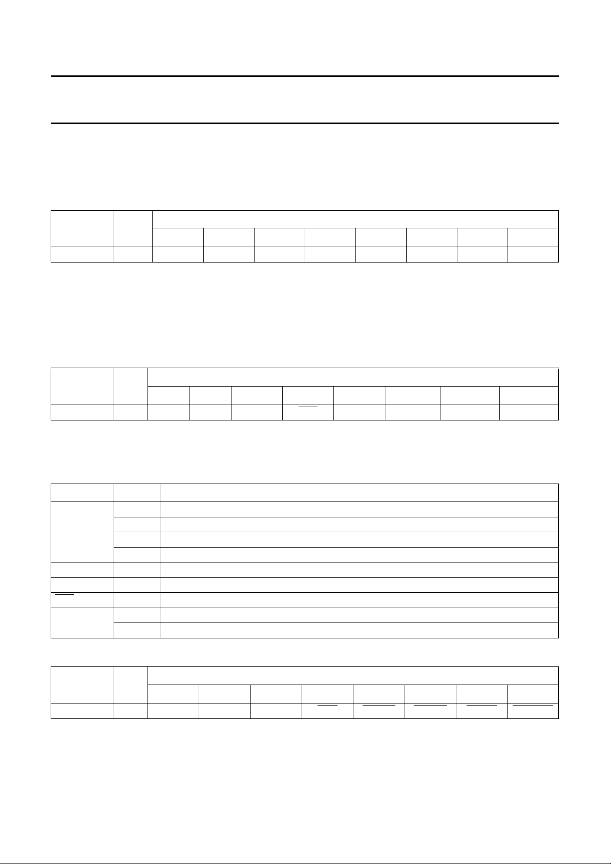
Table 14 Start clock doubler: 0xF091
MNEMONIC R/W
76543210
CLKSEL W −−−−−−−−
A write of any value to this address will engage the clock doubler. The state of the doubler may be obtained by reading
C_34_16 in BRGSEL (see Table 26). If this bit is set then the clock doubler is engaged. On power-on, the clock doubler
is disabled. Once the clock doubler is engaged, it can only be reset by one of the reset sources; a power-on reset, an
SCSI reset or a reset from the watch-dog timer. The clock doubler must not be engaged when a 34.8688 MHz clock is
connected to OSCIN (pin 120).
Table 15 General logic control register: 0xF0B9; note 1
MNEMONIC R/W
76 5 4 3 2 1 0
WTGCTL W −−PWMSEL
DATA BYTE
DATA BYTE
LED LA_MUTE RA_MUTE CHANNEL1 CHANNEL0
Note
1. Register 0xF0B9 controls the audio mixing, the LED and the PWM control.
Table 16 WTGCTL field descriptions
FIELD LOGIC DESCRIPTION
CHANNELS 00 mute
01 right data sent to both channels
10 left data sent to both channels
11 stereo
RA_MUTE − right channel digital mute
LA_MUTE − left channel digital mute
LED − active LOW control for the light emitting diode
PWMSEL 0 CD decoder output (default); e.g. CD-60 MOTO1 output
1 PWM output
Table 17 Drive switches register: 0xF0BA; note 1
MNEMONIC R/W
76543210
RDSW R −−−
DATA BYTE
HFD VOLUP VOLDN EJECT TRAYSW
Note
1. Register 0xF0BA is used for sensing the drive switches (note that the meaning of the switches is application specific).
1996 Jul 02 24
Page 25
Philips Semiconductors Preliminary specification
High performance Compact
SAA7390
Disc-Recordable (CD-R) controller
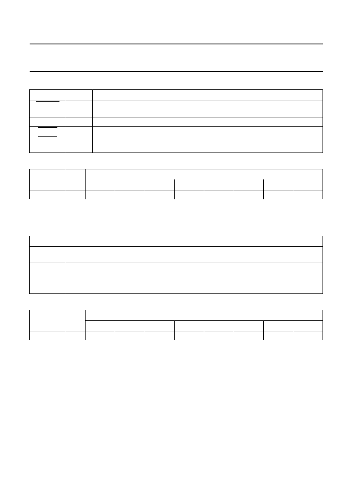
Table 18 RDSW field descriptions
FIELD LOGIC DESCRIPTION
TRAYSW 0 tray position in
1 tray position out
EJECT − user is requesting the drive tray to open (active LOW)
VOLDN − user is requesting a decrease in volume (active LOW)
VOLUP − user is requesting an increase in volume (active LOW)
HFD − high frequency detection; laser is on and focused (active LOW)
Table 19 Jumper status register: 0xF0C9; note 1
MNEMONIC R/W
76543210
RDJMPRS R RESERVED (2 to 0) ALO/PRE PAREN SCSIID2 SCSIID1 SCSIID0
Note
1. The bit fields for the jumpers are explained in Table 21 (note that the meaning of the jumpers is application specific).
DATA BYTE
Table 20 RDJMPRS field descriptions
FIELD DESCRIPTION
SCSIID SCSI identity. Installing pull-up shunts on the ID selection jumpers (DD2 to DD) sets the respective
SCSI ID bits HIGH on de-assertion of reset.
PAREN SCSI bus parity enable. Installing a pull-up shunt on DD3 sets this bit HIGH on de-assertion of reset.
The firmware should interpret this as SCSI bus parity enable.
ALO/PRE Allow/Prevent. Installing a pull-up shunt on DD4 sets this bit HIGH on de-assertion of reset.
Drive firmware interprets this as allowing access to media.
Table 21 General purpose bits: 0xF0C2; note 1
MNEMONIC R/W
76543210
GPIOCTL R/W GPDAT4 GPDIR4 GPDAT3 GPDIR3 GPDAT2 GPDIR2 GPDAT1 GPDIR1
Note
1. Register 0xF0C2 controls the direction and output state of the general purpose I/O bits on the SAA7390. Reading
the GPIO direction bits reflects the last value that was written to the register. The four GPIO data bits shows the
current value of the input signals in the input mode. In the output mode, the last value written to the output latches is
that which is read back.
DATA BYTE
1996 Jul 02 25
Page 26
Philips Semiconductors Preliminary specification
High performance Compact
SAA7390
Disc-Recordable (CD-R) controller
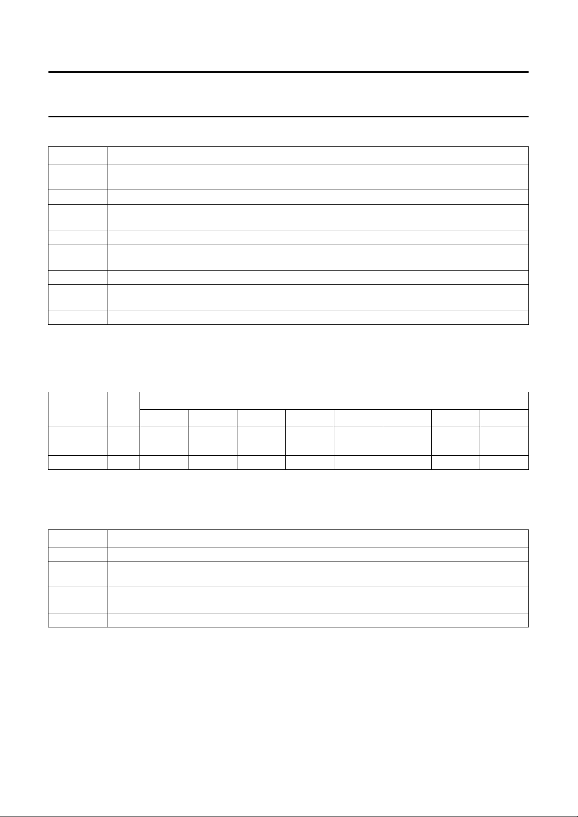
Table 22 GPIOCTL field descriptions
FIELD DESCRIPTION
GPDIR1 General purpose bit direction control. Default LOW puts GPIO1 into the input mode, setting this HIGH
puts GPIO1 in output mode.
GPDAT1 GPIO1 data bit.
GPDIR2 General purpose bit direction control. Default LOW puts GPIO2 into the input mode, setting this HIGH
puts GPIO2 in output mode.
GPDAT2 GPIO2 data bit.
GPDIR3 General purpose bit direction control. Default LOW puts GPIO3 into the input mode, setting this HIGH
puts GPIO3 in output mode.
GPDAT3 GPIO3 data bit.
GPDIR4 General purpose bit direction control. Default LOW puts GPIO4 into the input mode, setting this HIGH
puts GPIO4 in output mode.
GPDAT4 GPIO4 data bit.
9.1 S2B UART registers
This section describes the registers used for the S2B UART control.
Table 23 S2B UART transmit, receive and status buffer: 0xF0A1, F0A2 and F0A3; note 1
MNEMONIC R/W
76543210
WTS2B W DATA7 DATA6 DATA5 DATA4 DATA3 DATA2 DATA1 DATA0
RDS2B R DATA7 DATA6 DATA5 DATA4 DATA3 DATA2 DATA1 DATA0
S2BSTAT R −−−−TXDRDY PE OVRRUN RXDRDY
Note
1. WTS2B is for the transmit data byte from the S2B UART and RDS2B is for the receive data byte from the S2B UART.
Table 24 S2BSTAT field descriptions
FIELD DESCRIPTION
RXDRDY logic 1 indicates that the receive data is valid
OVRRUN logic 1 indicates that the data in the receive buffer was not read before it was over written by the next
byte
PE logic 1 indicates that a parity error was detected in the receive data byte; this is usually caused by the
wrong baud rate
TXDRDY logic 1 indicates that the transmit data buffer is empty and ready for another byte
DATA BYTE
1996 Jul 02 26
Page 27
Philips Semiconductors Preliminary specification
High performance Compact
SAA7390
Disc-Recordable (CD-R) controller
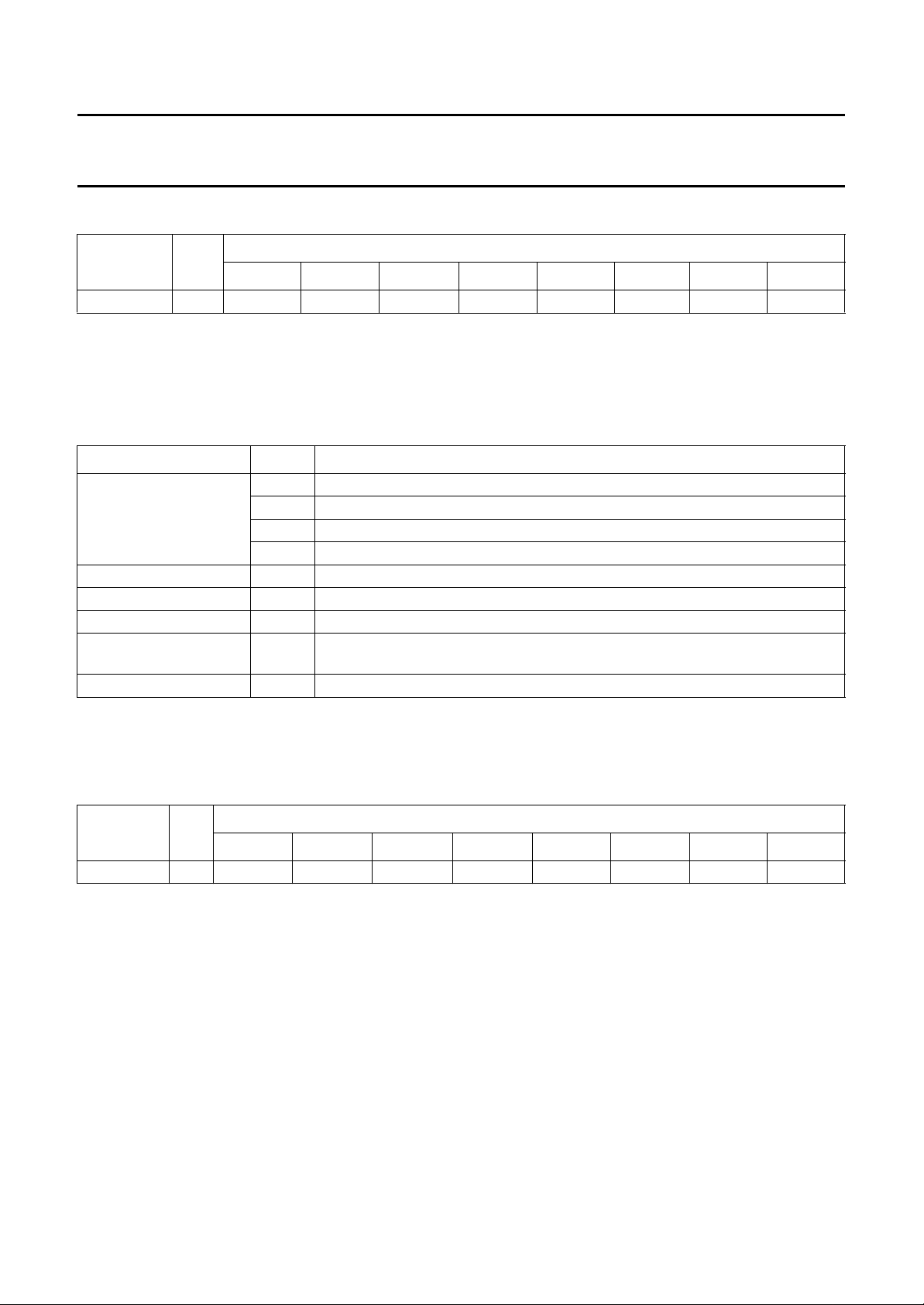
Table 25 Baud rate generator control: 0xF0C0; note 1
MNEMONIC R/W
76543210
BRGSEL R/W C_34_16 LOCK EVENPAR INVSUBC INVQ − S2BSEL1 S2BSEL0
Note
1. Register 0xF0C0 controls the S2B UART baud rate and selective inversion of the sub-code information. Control over
the parity and the clock doubler is also included together with the ability to invert the sub-code and Q-channel
information.
Table 26 BRGSEL field descriptions
FIELD LOGIC DESCRIPTION
S2BSEL1 and S2BSEL0 00 31.25 kbaud transfer rate
01 62.5 kbaud transfer rate
10 187.5 kbaud transfer rate
11 not specified
INVQ − inverts all Q-channel information if set
INVSUBC − inverts all sub-code information if set
EVENPAR − selects even parity for S2B UART is set
LOCK − read only information; indicates clock synthesizer is stable (after reset) and it is
ready to set C_34_16
C_34_16 − once LOCK is HIGH, asserting this bit engages the clock doubler
DATA BYTE
9.2 SPI UART registers
This section describes the registers used for SPI control.
Table 27 Serial communication control: 0xF0F1; note 1
MNEMONIC R/W
76543210
SC_CTL R/W SSU_REP SSD_REP CSU_REP CSD_REP SSU_SEL SSD_SEL CSU_SEL CSD_SEL
Note
1. Register 0xF0F1 selects and reports the signals and edges of interrupts required to control the basic engine.
The least significant four bits perform the selection and are read/write. If both the rising and falling edges are set then
both signal edges cause interrupts. If both rising and falling edges are cleared then neither edge will cause an
interrupt. The most significant four bits report which edge of which signal caused the interrupt and are read-only; the
interrupt generated by these bits is cleared by reading register 0xF0F1.
DATA BYTE
1996 Jul 02 27
Page 28
Philips Semiconductors Preliminary specification
High performance Compact
SAA7390
Disc-Recordable (CD-R) controller
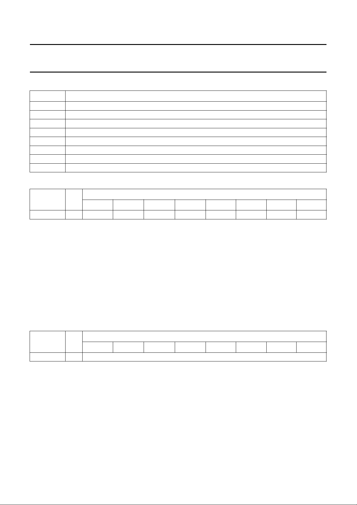
Table 28 UARTCTL field descriptions
FIELD DESCRIPTION
CSD_SEL elects COM_SYNC falling edge when set
CSU_SEL selects COM_SYNC rising edge when set
SSD_SEL selects SYS_SYNC falling edge when set
SSU_SEL selects SYS_SYNC rising edge when set
CSD_REP reports COM_SYNC falling edge when set
CSU_REP reports COM_SYNC rising edge when set
SSD_REP reports SYS_SYNC falling edge when set
SSU_REP reports SYS_SYNC rising edge when set
Table 29 SAA7390 to basic engine communication port: 0xF0C4; note 1
MNEMONIC R/W
76543210
SERCOM R/W DATA7 DATA6 DATA5 DATA4 DATA3 DATA2 DATA1 DATA0
Note
1. Register 0xF0C4 provides a serial communication path to the basic engine processor. Writing a byte to this register
automatically clocks the bits to the other processor. As the bits shift out, a byte from the basic engine processor is
shifted in. The bit rate is 2 Mbits/s. Handshake with the basic engine is accomplished with COM_ACK.
DATA BYTE
9.3 Track Descriptor Block (TDB) generation
A special mode has been included to support automatic TDB generation. Basically, the host writes one frame of the TDB
into the buffer and programs its address into TDB. Then the number of frames to repeat this pattern is programmed in
TDB_CNT. Once this has been carried out, TDB_EN in FEBMCTL is set. When the frame counter equals the contents
of TDB, the TDB frame will be repeated as many times as programmed by TDB_CNT. If more than 256 frames are
required for the TDB, TDB_CNT can be read back and re-programmed with a new value. This action must be carried out
as soon as possible after an end-of-frame to prevent the count value from being corrupted.
Table 30 Track descriptor block count: 0xF08F; note 1
MNEMONIC R/W
76543210
TDB_CNT R/W TDB count 7 to TDB count 0
Note
1. The loadable down counter holds the TDB frame count. TDB_CNT can be read while a TDB is being sent to the
CDB2 and may be re-written with a new value to extend the length of the TDB beyond 256 frames; which should be
carried out as soon as possible after an end-of-frame.
DATA BYTE
1996 Jul 02 28
Page 29
Philips Semiconductors Preliminary specification
High performance Compact
SAA7390
Disc-Recordable (CD-R) controller
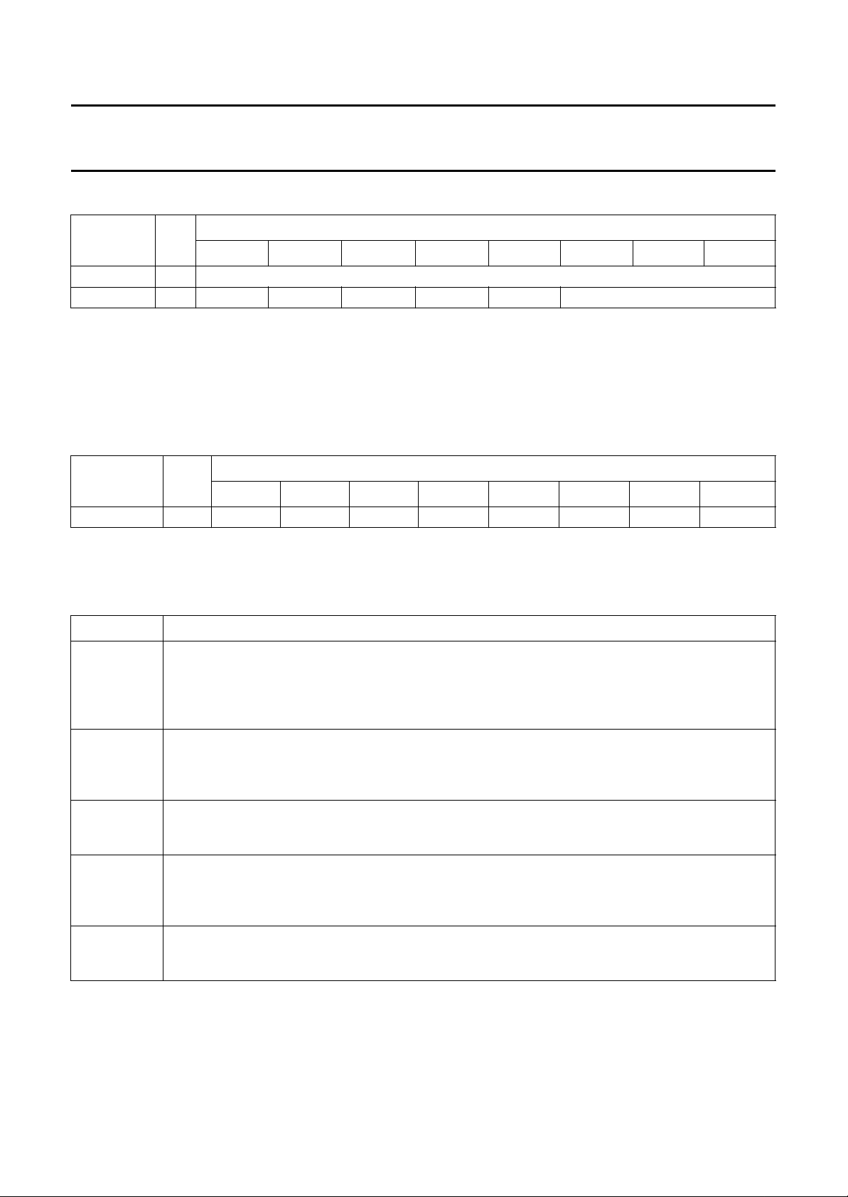
Table 31 Track descriptor block address: 0xF096 and 0xF097; note 1
MNEMONIC R/W
76543210
TDB R/W TDB address 7 to TDB address 0
TDB R/W −−−−− TDB address 10 to 8
Note
1. Registers 0xF096 and 0xF097 contain the frame address of the TDB. When the buffer manager frame count equals
the contents of this register and the TDB_EN bit is set in BMFECTL, the frame counter will not be allowed to
increment until TDB_CNT equals zero.
9.4 Miscellaneous control registers
Table 32 Host interface direction and audio mode control: 0xF0C1; note 1
MNEMONIC R/W
76543210
WTDIR R/W −−−CBSB OVER4X BSB HOSTDIR AUTOSTR
DATA BYTE
DATA BYTE
Note
1. Register 0xF0C1 controls the data path to the host interface and some audio functions.
Table 33 WTDIR field descriptions
FIELD DESCRIPTION
AUTOSTR Automatic store; default is off. When set HIGH, the front-end will automatically begin storing data or
audio when the contents of the header/Q-channel registers equals the contents of the STRTMIN,
STRTSEC and STRTFRM registers. If a header/Q-channel error occurs to invalidate the address,
auto-store is inhibited. Storing of data will continue until the contents of the STOPCNT equals zero, at
which time it will automatically stop.
HOSTDIR Host direction; default LOW. This selects the microcontroller data path to the SCSI interface. Setting
this HIGH selects the buffer managers DMA path. When using a 53CF92A, this should be set and left
HIGH since the microcontroller has a separate command path into the 53CF92A whereas the
53CF90B requires the buffer manager and microcontroller to share the same path.
BSB Byte swap bit. Defaults to swapping the most significant byte and least significant byte in the audio
mode such that the least significant byte of all audio samples is stored at even addresses in the
DRAM. Setting this HIGH causes the audio data to be stored in the same way as in the data mode.
OVER4X 4× over-sampling bit selection; default LOW select transmit, or no over-sampling, mode for the
sub-code and C-flag UARTs. Setting this bit HIGH will cause the sub-code and C-flag data to be
sampled at one quarter the data rate allowing Q-channel information to be correctly stored in the
registers while the CD-60 is outputting audio data at 4× over-sampling.
CBSB CBD2 byte swap bit; default LOW allows data from the DRAM buffer to be sent to the CDB2 normally
(data mode). When set HIGH, the high byte and low byte are swapped since data from the host will be
swapped. As a result, Red book in the bypass mode will be correctly aligned.
1996 Jul 02 29
Page 30
Philips Semiconductors Preliminary specification
High performance Compact
SAA7390
Disc-Recordable (CD-R) controller
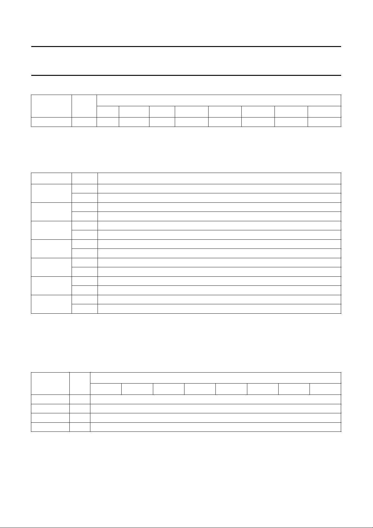
Table 34 SCSI mode control register: 0xF0FD; note 1
MNEMONIC R/W
76543210
HOSTMOD R/W − SELCF92 FAST OFF_ADR OFF_END OFF_STR RD_BUF BYT/PAG
Note
1. Register 0xF0FD controls the operation of the interface to the host interface controller. The outputs of these registers
are used to directly control DRAM access cycles, and will affect any current DRAM cycle in progress.
Table 35 HOSTMOD field descriptions
FIELD LOGIC DESCRIPTION
BYT/PAG 0 host interface DRAM byte mode access
1 host interface DRAM page mode access
RD_BUF 0 host interface read/write control; read from buffer memory
1 host interface read/write control; write to buffer memory
OFF_STR 0 host interface offset start A/B control; select A registers
1 host interface offset start A/B control; select B registers
OFF_END 0 host interface offset end A/B control; select A registers
1 host interface offset end A/B control; select B registers
OFF_ADR 0 host interface transfers use only A registers
1 host interface transfers use A and B registers
FAST 0 3 cycles host interface burst accesses from buffer
1 2 cycles host interface burst accesses from buffer
SELCF92 0 DRAM timing optimized for 53CF90
1 DRAM timing optimized for 53CF92
DATA BYTE
10 FRONT-END
This chapter explains the information of the front-end circuitry.
10.1 Minute-second frame addressing and header information
Table 36 Header mode and MSF from block decoder: 0xF092, F093, F09A and F09B; note 1
MNEMONIC R/W
76543210
HDRMODE R MODE7 to MODE0
HDRMINS R MINUTES7 to MINUTES0
HDRSEC R SECONDS7 to SECONDS0
HDRFRM R FRAME7 to FRAME0
Note
1. These registers contain the mode, minute, second and frame information from the header when in data mode. This
data is valid whenever the HDDRDY bit in the RDDSTAT register is set. In audio mode, the MSF address is taken
from the Q-channel information.
1996 Jul 02 30
DATA BYTE
Page 31
Philips Semiconductors Preliminary specification
High performance Compact
SAA7390
Disc-Recordable (CD-R) controller
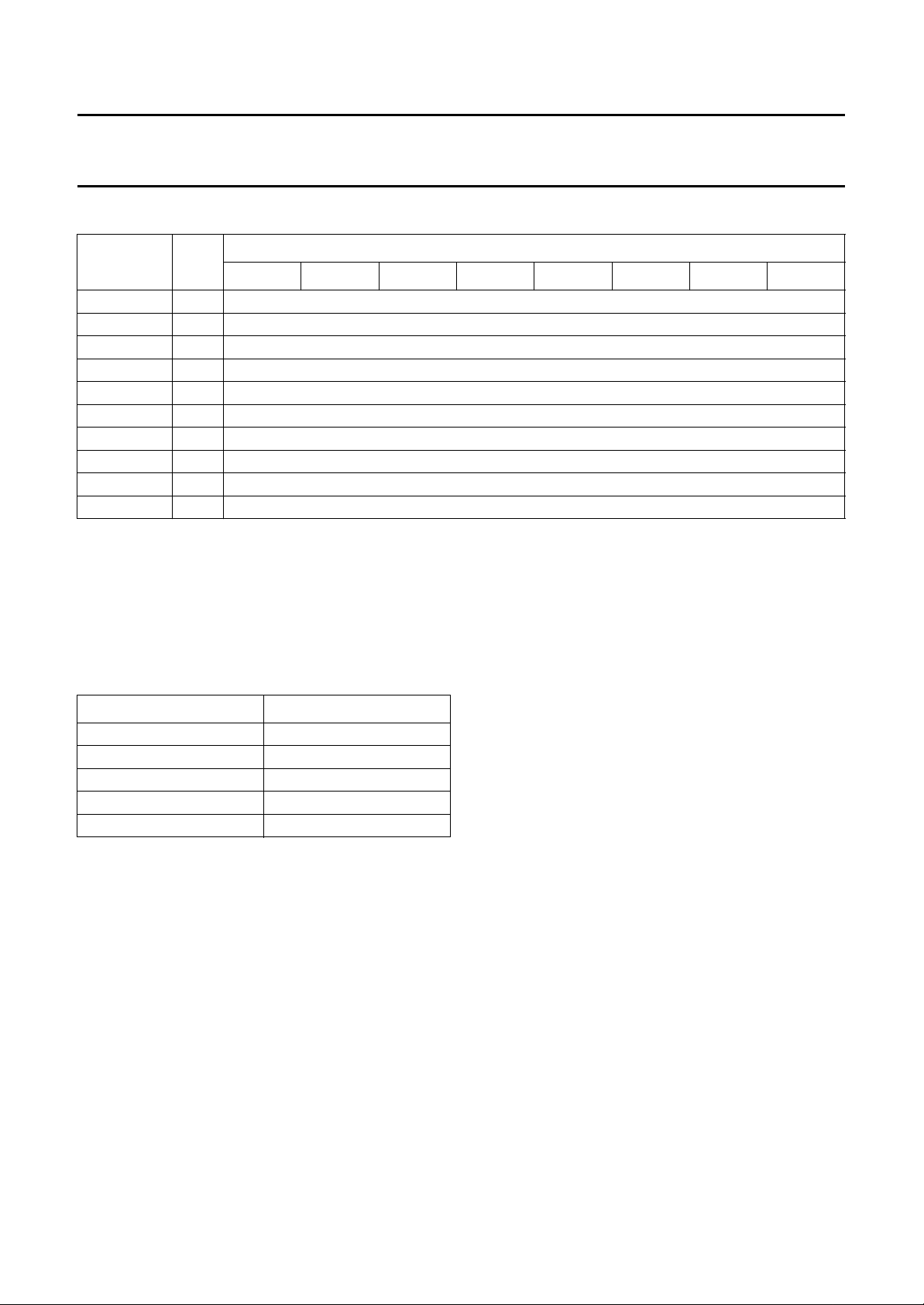
Table 37 Q-channel information: 0xF084, F094, F095, F0A9, F0AA, F0AB, F0B1, F0B2, F0CF and F0FA,; note 1
MNEMONIC R/W
76543210
QZERO R ZERO7 to ZERO0
QTNO R TRACK7 to TRACK0
QINDX R INDEX7 to INDEX0
QMODE R MODE7 to MODE0
QAMIN R ABSMIN7 to ABSMIN0
QASEC R ABSSEC7 to ABSSEC0
QAFRM R ABSFRM7 to ABSFRM0
QMIN R RELMIN7 to RELMIN0
QSEC R RELSEC7 to RELSEC0
QFRM R RELFRM7 to RELFRM0
Note
1. These registers contain the information taken from the raw sub-channel information from the CD decoder. Due to the
fact that this data has not had any error correction applied to it, it is necessary to perform a CRC check for validity.
Twelve bytes of Q-channel information are assembled from each sector of data; the last two bytes contain the CRC
parity. Therefore the validity of the contents of these registers can only be determined after the last bit has been
loaded and checked.
DATA BYTE
Table 38 Times from QCHRDY to BADQ (RDDSTAT)
SPEED TIME (µs)
n = 1 2177
n = 2 1089
n = 4 545
n = 6 363
n = 8 273
For example, at the n = 4 data rate, the BADQ flag
(in RDDSTAT) should be checked 545 µs after the
QFRMRDY interrupt (from RDDSTAT) is asserted.
If BADQ is LOW then the contents of the Q-channel
registers are valid; otherwise the CRC check failed and the
Q-channel information may be incorrect. If the data clock
is running (ECMD LOW or ENABRED HIGH) then BADQ
will be valid until the end of the sector; otherwise BADQ is
valid until the end of the next Q frame.
1996 Jul 02 31
Page 32
Philips Semiconductors Preliminary specification
High performance Compact
SAA7390
Disc-Recordable (CD-R) controller
10.2 Front-end status and control
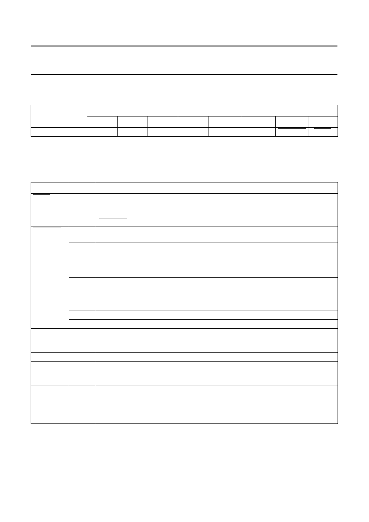
Table 39 Front-end control: 0xF0BB; note 1
MNEMONIC R/W
7654 3 2 10
FECTL R/W SIM_EOF RSMD BREAK RWMD ENABRED AUDMODE
Note
1. Register 0xF0BB controls the front-end of the SAA7390. The naming convention used here is similar to that used in
the block decoders.
Table 40 FECTL field descriptions
FIELD LOGIC DESCRIPTION
ECMD 0 Data is shifted in and stored when the next synchronization pattern is detected;
(SYNASYN = 1 and AUDMODE = 0).
1 Data flow stop just before next synchronization pattern.
(SYNASYN = 1).
SYNASYN Synchronous/asynchronous selection; this controls the method by which data is started and
stopped by the block decoder, only operates in data mode.
0 Causes a ‘panic stop’. A partial frame will reside in current and subsequent buffers unless
SIM_EOF is set then cleared; (ECMD = 1).
1 Data is started and stopped on frame boundaries (on synchronization patterns).
AUDMODE 0 Data mode. Cleared on reset.
1 Audio mode, where the bit clock is shifted to accommodate EIAJ format. HQRDY in
INTRFLG follows HDRRDY in data mode and QFRMDRY in audio mode.
ENABRED Enable red book to data path; while in audio mode, this is equivalent to
mode. No asynchronous stop is provided in the audio mode.
0 Data flow will stop when the next F1 C-flag is detected. Cleared on a reset condition.
1 Red book data is input to buffer after the detection of the next F1 C-flag.
RWMD − This must be pulsed HIGH then LOW every 212 ms to prevent the watch-dog timer from
resetting the SAA7390 and the drive. The length of the reset pulse is 967 µs. If RWMD is set,
the watch-dog timer is disabled.
BREAK − When set, the S2B UART transmitter output is held HIGH.
RSMD − When the pulse is HIGH then LOW, the block decoder begins to search for a synchronization
pattern in the data bitstream. Once a synchronization pattern is found, MODE, MINS, SECS,
and FRMS become valid.
SIM_EOF − This provides a firmware reset to the frame sequencer and parts of the buffer manager.
This would be required if an asynchronous stop of the data stream occurs. Pulsing this HIGH
then LOW resets all counters and establishes a ‘beginning of frame’ state. DCOACT in
RDDST AT must be LOW to allow SIM_EOF to have any effect. If SIM_EOF is set, no data or
sub-code is stored in the buffer.
DATA BYTE
SYNASYN ECMD
ECMD is set on a reset condition;
ECMD in the data
1996 Jul 02 32
Page 33

Philips Semiconductors Preliminary specification
High performance Compact
SAA7390
Disc-Recordable (CD-R) controller
Table 41 Read status register: 0xF0C3; note 1
MNEMONIC R/W
76 5 4321 0
RDDSTAT R DCOTACT BADQ QFRMRDY HDRRDY HDRERR CRCERR DATERR SYNCERR
Note
1. The information in register 0xF0C3 is a copy of the status byte written to the data buffer at the end of every frame.
SYNCERR, DATERR and CRCERR are essentially unusable since they are valid only long enough to be written to
the buffer.
Table 42 RDDSTAT field descriptions
FIELD LOGIC DESCRIPTION
SYNCERR 0 Good synchronization detected (valid for 120 ns at the end of a sector).
DATERR 0 Good data (valid for 120 ns at the end of a sector).
CRCERR 0 Good CRC (valid for 120 ns at the end of a sector).
HDRERR 0 Good header.
If the automatic storage is selected, assertion of HDRERR inhibits data storage.
1 EFAB during reception of header (valid while HDRRDY set).
If the automatic storage is selected, assertion of HDRERR inhibits data storage.
HDRRDY − When set, a valid header is available. If the header is not read within a frame time, this
remains set until the next synchronization pattern and will be set again when the next
header arrives. It is cleared when any of the header bytes are read. This bit generates an
interrupt to the microcontroller when in data mode.
QFRMRDY − When set, all ten Q-channel bytes are received waiting to be read (BADQ is known). It is
reset at the end of frame or when any of the Q-channel bytes are read. This bit generates an
interrupt to the microcontroller when in audio mode.
BADQ − If Q-channel information failed CRC then BADQ is set. It is reset on next good CRC check or
on end of frame if DCOACT is running. If DCOACT is not running (i.e. audio mode) BADQ is
reset on next detection of sub-code gap. If AUTOSTR in WTDIR is selected, assertion of
BADQ inhibits audio data storage.
DCOTACT − Set when data is being shifted an and stored in the buffer: this will remain HIGH for the
entire transmission.
DATA BYTE
1996 Jul 02 33
Page 34

Philips Semiconductors Preliminary specification
High performance Compact
Disc-Recordable (CD-R) controller
11 BUFFER MANAGER
11.1 Front-end to buffer manager interface
The buffer manager interface to the front-end is write only
with no handshaking. The front-end passes one byte of
data and a write strobe to the buffer manager; this byte will
be one of five types of data (see Table 44). The data byte
is latched and the interface is given the highest priority
thus no wait signal is required. The other signals passed
from the front-end logic are an end-of-frame strobe (which
is the same as the status byte write strobe), a
software-generated reset pulse (used to reset the
front-end counters), and a reset pulse for the Q-channel
and sub-code offset counters.
Table 43 Data types from the front-end
START END LENGTH DATA TYPE
0x000 0x92F 0x930 header, data and parity
0x930 0x93F 0x010 Q-channel
0x940 0x99F 0x060 sub-channel
0x9A0 0xAC5 0x126 error flags
0xBDE 0xBDE 0x001 status byte
The buffer manager provides the remainder of the logic to
write the data into the RAM and keep track of the frame
addresses and offset addresses. This logic consists of a
12-bit frame offset counter FEOFF, for data and an 11-bit
frame counter; this is a relative frame number and is not
related to the CD-ROM frame number. Offset counters are
also provided for the four other types of data. The other
offset address generators are based on fixed addresses,
and they will be loaded with the start address at the
beginning of each frame. The five types of data from the
front-end are loaded into the frame map as shown in
Table 44.
SAA7390
Initially the front-end frame counter and all of the offset
counters are cleared by reset or loaded with the contents
of FEFRM# when the last frame as specified by LASTFRM
is filled; therefore FEFRM# should be loaded with the
required starting frame number. FEFRM# will load the
counter immediately if FEWBLK from BMFECTL is clear.
If TDB_EN in BMFECLT is set then one frame may be read
multiple times from memory; TDB selects the frame to be
read and TDB_CNT determines the number of times the
frame will be repeated. When this process is active, the
frame counter will not increment until TDB_CNT reaches
zero.
LASTFRM establishes the limit of the frame memory. This
register should be loaded with the required number of
frames; the amount of memory used is 3 kbytes times the
number of frames. The front-end frame address counter
uses this value to determine the correct location to re-load
the counter to the starting frame number, FEFRM#.
The frame counter and the frame data offset counter may
be loaded by the microcontroller; this allows the starting
frame number (via FEFRM#) to be modified by the
microcontroller, and the frame data offset counter
(FEFRMOFF) may be loaded for test purposes.
Once the data load process starts, the offset counter
(FEOFF) increments after each byte is written into
memory. This process continues until an end-of-frame
signal is received from the front-end logic. If an error
occurs and the offset counter increments past the
maximum 2352, an interrupt will be issued to the
microcontroller.
1996 Jul 02 34
Page 35
Philips Semiconductors Preliminary specification
High performance Compact
SAA7390
Disc-Recordable (CD-R) controller
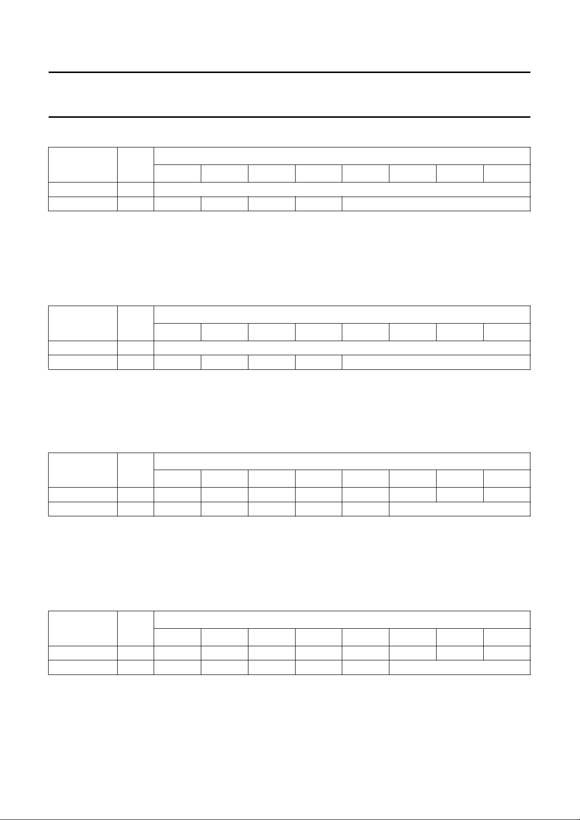
Table 44 Front-end frame offset: 0xF0E2, F0E3; note 1
MNEMONIC R/W
76543210
FEFRMOFF R/W OFFSET7 to OFFSET0
FEFRMOFF R/W −−−− OFFSET11 to OFFSET8
Note
1. This register allows the front-end frame offset counter to be read and reloaded. The counter associated with these
registers is loaded after the most significant byte is written; the least significant byte must be written first to ensure
that the counter is loaded correctly. If a DRAM access is in progress that uses the address from the counter, the
update will be delayed until the access is complete.
Table 45 Front-end offset counter: 0xF09E, 0xF09F; note 1
MNEMONIC R/W
76543210
FEOFF R/W OFFSET7 to OFFSET0
FEOFF R/W −−−− OFFSET11 to OFFSET8
DATA BYTE
DATA BYTE
Note
1. These registers access the actual counter for the front-end offset counter and therefore change rapidly during a
transfer. The front-end frame offset counter is cleared after reset and after each frame is loaded into the buffer
memory. Therefore, FEFRMOFF should not be loaded during normal operation.
Table 46 Front-end offset counter: 0xF0E4, 0xF0E5; note 1
MNEMONIC R/W
76543210
FEFRM# R/W FRAME7 FRAME6 FRAME5 FRAME4 FRAME3 FRAME2 FRAME1 FRAME0
FEFRM# R/W −−−−− FRAME10 to FRAME8
Note
1. This register allows the front-end frame number counter to be read and reloaded. The counter associated with these
registers is loaded after the most significant byte is written; the least significant byte must be written first to ensure
that the counter is loaded correctly. If a DRAM access is in progress that uses the address from the counter, the
update will be delayed until the access is completed.
Table 47 Last frame number for storage: 0xF0F8, F0F9; note 1
MNEMONIC R/W
76543210
LASTFRM R/W FRAME7 FRAME6 FRAME5 FRAME4 FRAME3 FRAME2 FRAME1 FRAME0
LASTFRM R/W −−−−− FRAME10 to FRAME8
DATA BYTE
DATA BYTE
Note
1. These registers are used by the buffer manager to set the top of frame storage memory (wrap point). Any memory
past this point is available for general usage by the microcontroller. The outputs of the registers are used directly to
control DRAM access cycles, and will affect any current DRAM cycle in progress.
1996 Jul 02 35
Page 36

Philips Semiconductors Preliminary specification
High performance Compact
SAA7390
Disc-Recordable (CD-R) controller
Table 48 Buffer manager front-end control: 0xF0E1
MNEMONIC R/W
76543210
BMFECTL R/W −−−−STOP FEWBLK HW_BLK TDB_EN
Table 49 BMFECTL field descriptions
FIELD LOGIC DESCRIPTION
TDB_EN − Track Descriptor Block (TDB) enable; default LOW. When set, this causes the buffer
manager to continuously output the frame addressed by TBDL/TDBH for as many frames as
programmed into TDB_CNT . TDB_CNT can be read and re-initialized while the TDB is being
sent to the CDB2 to extend the count beyond 256.
HW_BLK − Host write block. If set HIGH, this bit will prevent a write to the host start frame number
register (HOSTSFRM) for immediately changing the host frame counter (HOSTCFRM).
The new value will be loaded at the next roll-over; a roll-over occurs when the host frame
counter reaches the maximum frame number (LASTHOST) and is reloaded with the host
start frame number.
FEWBLK − Front-end write block. If set HIGH, this bit will prevent a write to the front-end start frame
number register (FEFRM#) from immediately changing the front-end counter. The new value
will be loaded at the next roll-over; a roll-over occurs when the front-end frame counter
reaches the maximum frame number (LASTFRM) and is reloaded with the front-end start
frame number (FEFRM#).
STOP 0 Automatic START control registers are selected.
1 Automatic STOP control registers are selected.
DATA BYTE
11.2 Microcontroller to buffer manager interface
The microcontroller interface allows the microcontroller to
read or write any register or the frame store memory.
Frame and offset registers are used to update the counters
after the most significant byte has been loaded. Frame
store memory is addressed using a frame number register
controller by the microcontroller. Logic is provided to allow
the frame number of the last complete frame received
(LSTCMPFM) from the front-end to be read by the
microcontroller for the purpose of setting the
microcontroller frame address.
Memory beyond the last frame number is available to the
microcontroller using the microcontroller bottom 32 kbytes
located at 0x0000 to 0x7FFF. The 4 kbytes segment at
0x8000 to 0x8FFF is used to address the current frame
memory. Also, the next frame may be accessed at
0x9000 to 0x9FFF, and the current frame plus 2 may be
accessed at 0xA000 to 0xAFFF.
A page register is provided to allow the microcontroller to
address the complete memory range in 32 kbytes pages.
All microcontroller accesses to memory are single byte
read or write cycles.
All microcontroller accesses to memory will generate a
wait state. If no other accesses to memory are in progress
then a minimum wait state cycle will be generated. If,
however, other cycles are in progress then the
microcontroller is forced to wait until the lower priority
access cycles finish and any high priority access cycles
are completed. The worst case wait is four complete
access cycles; a total of 20 clock cycles.
1996 Jul 02 36
Page 37
Philips Semiconductors Preliminary specification
High performance Compact
SAA7390
Disc-Recordable (CD-R) controller
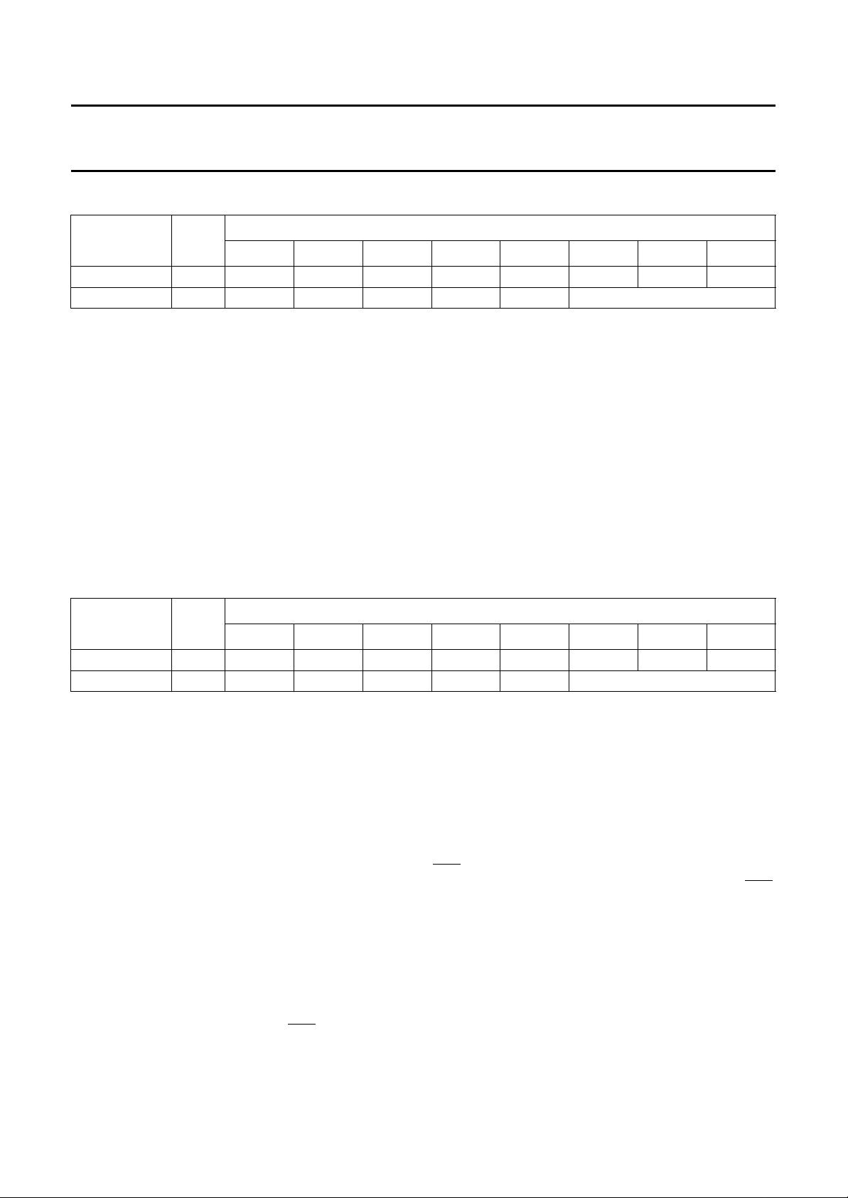
Table 50 Last complete frame number: 0xF0E6, F0E7; note 1
MNEMONIC R/W
76543210
LSTCMPFM R FRAME7 FRAME6 FRAME5 FRAME4 FRAME3 FRAME2 FRAME1 FRAME0
LSTCMPFM R −−−−− FRAME10 to FRAME8
Note
1. This register provides the address of the last complete frame that was received.
11.3 ECC to buffer manager interface
The ECC logic is able to access the buffer manager frame memory in either byte or burst mode. The ECC logic provides
an offset address and uses a frame address programmed by the microcontroller, ECCFRM#. The logic can write a single
byte or variable number of bytes. In the event of an access to a variable number of bytes, the ECC logic will assert the
signal BURST and EREQ to indicate that a large number of cycles are requested.
For each read or write cycle, the buffer manager will toggle EACK HIGH for one clock cycle to indicate that one byte of
data has been read from or written to the memory. A single byte cycle will be the same with the exception that BURST
will remain negated (LOW). In the event of a higher priority memory access request during a burst cycle, EACK will
remain LOW for the duration of the higher priority access cycle. At the end of the higher priority access, the burst cycle
will resume and EACK will again toggle HIGH after each read or write is completed.
DATA BYTE
Table 51 ECC frame number address registers: 0xF0F4, F0F5; note 1
MNEMONIC R/W
ECCFRM# R/W FRAME7 FRAME6 FRAME5 FRAME4 FRAME3 FRAME2 FRAME1 FRAME0
ECCFRM# R/W −−−−− FRAME10 to FRAME8
Note
1. These registers provide the frame number address for ECC access to memory. The counter associated with these
registers is loaded after the most significant byte is written; the least significant byte must be written first to ensure
that the counter is loaded correctly. If a DRAM access is in progress that uses the address from the counter, the
update will be delayed until the access is completed.
ECCFRM# is used to determine the frame address for
all ECC operations. This register must be reloaded for
each frame accessed by the ECC.
11.4 SCSI to buffer manager interface
The host interface registers should be loaded prior to
starting an host interface transfer. The HOSTMOD register
should be loaded first. BYT/PAG and FAST from this
register are used to control the type of DRAM access used
by the host interface. If BYT/PAG is HIGH then burst mode
access cycles are selected; multiple
are used to access data as fast as possible. FAST allows
the speed of the burst cycle to be selected; for most host
76543210
CAS access cycles
DATA BYTE
controllers this bit is set LOW to select three clocks per
CAS cycle. For faster host access, FAST should be
asserted and the host burst cycle uses two clocks perCAS
cycle.
RD_BUF from HOSTMOD controls the direction of data
flow to the buffer memory; this bit is kept LOW to allow
reading of data from the DRAM buffer. If RD_BUF is
asserted then host data will be written to the DRAM buffer.
OFF_ADR from HOSTMOD is used to select between one
and two offset mode for the host transfer. OFF_ADR LOW
selects single offset mode in which one block of data is
transferred for each frame of the buffer.
1996 Jul 02 37
Page 38

Philips Semiconductors Preliminary specification
High performance Compact
Disc-Recordable (CD-R) controller
The transfer block is specified by registers HOSTOFFS
and HOSTOFFE. For each frame, the transfer will start at
the address specified by HOSTOFFS and continue until
the address specified by HOSTOFFE is transferred.
After each block is transferred, the frame address
HOSTCFRM will be incremented and the transfer will
continue with the same address block from the next frame.
If OFF_ADR is set, then two blocks of data are transferred.
In the two offset mode, both HOSTOFFS and HOSTOFFE
are used to access two independent register pairs; for
simplicity, these are called the A registers and the B
registers. In this event, the transfer for each frame is a two
step process.
First, the offset block specified by HOSTOFFS-A and
HOSTOFFE-A is transferred; the transfer address range is
from HOSTOFFS-A to HOSTOFFE-A and includes both
the start and end addresses. After the first offset block is
transferred, the second offset block as specified by
HOSTOFFS-B and HOSTOFFE-B is transferred.
The frame address will not be incremented until after both
offset blocks are transferred. Once both offset blocks are
transferred, the frame address is incremented and again
the two offset blocks are transferred for the next frame.
Reading and writing of the A and the B registers is
controlled by an automatic switching after the most
significant bytes of the registers are written.
After power-up or reset the pointer to the A registers will be
selected. If the dual offset mode is selected, the A/B switch
will be toggled when the most significant bytes of the
registers are written; either the most significant bytes of
SAA7390
HOSTOFFS or HOSTOFFE. Any future reads or writes will
access the B registers.
The process of loading and reading the two host offset
address pairs can be monitored and controlled by
OFF_STR and OFF_END from HOSTMOD. Reading
OFF_STR shows the status of the A/B switch for the
HOSTOFFS-A/B registers; reading OFF_END shows the
status of the A/B switch for the HOSTOFFE-A/B registers.
A write to HOSTMOD with OFF_STR LOW will clear the
A/B switch for the HOSTOFFS registers; a write to
HOSTMOD with OFF_END LOW will clear the A/B switch
for the HOSTOFFE registers.
HOSTSFRM is used to determine the starting frame
address for all host operations. The associated counter is
automatically incremented after each frame, and wraps
back onto HOSTSFRM when the last frame as specified by
LSTFHOST is transferred. To update the host frame
address counter, HOSTSFRM must be rewritten.
The current host frame address is available by reading
HOSTCFRM.
The SCSIOFFS registers access either one or two register
pairs as controlled by SCSIMOD. SCSIOFFS determines
the starting offset address for a host transfer.
The SCSIOFFE register accesses either one or two
register pairs as controlled by SCSIMOD. SCSIOFFE
determines the ending offset address for a host transfer.
Remarks:
• If two offset pairs are used, theA start offset must be written last to ensure that the correct offset start address is loaded
into the counter.
• In the two offset mode, reading the register after loading is not possible due to the automatic switching feature; if the
A offset pair is written, and the register pair is read, the B offset pair would be read.
Table 52 Host interface offset counter: 0xF09C, F09D; note 1
MNEMONIC R/W
76543210
HOFF R/W OFFSET7 to OFFSET0
HOFF R/W −−−− OFFSET11 to OFFSET8
Note
1. These addresses access the actual counter of the host interface offset counter and therefore rapidly change during
host interface transfers.
1996 Jul 02 38
DATA BYTE
Page 39
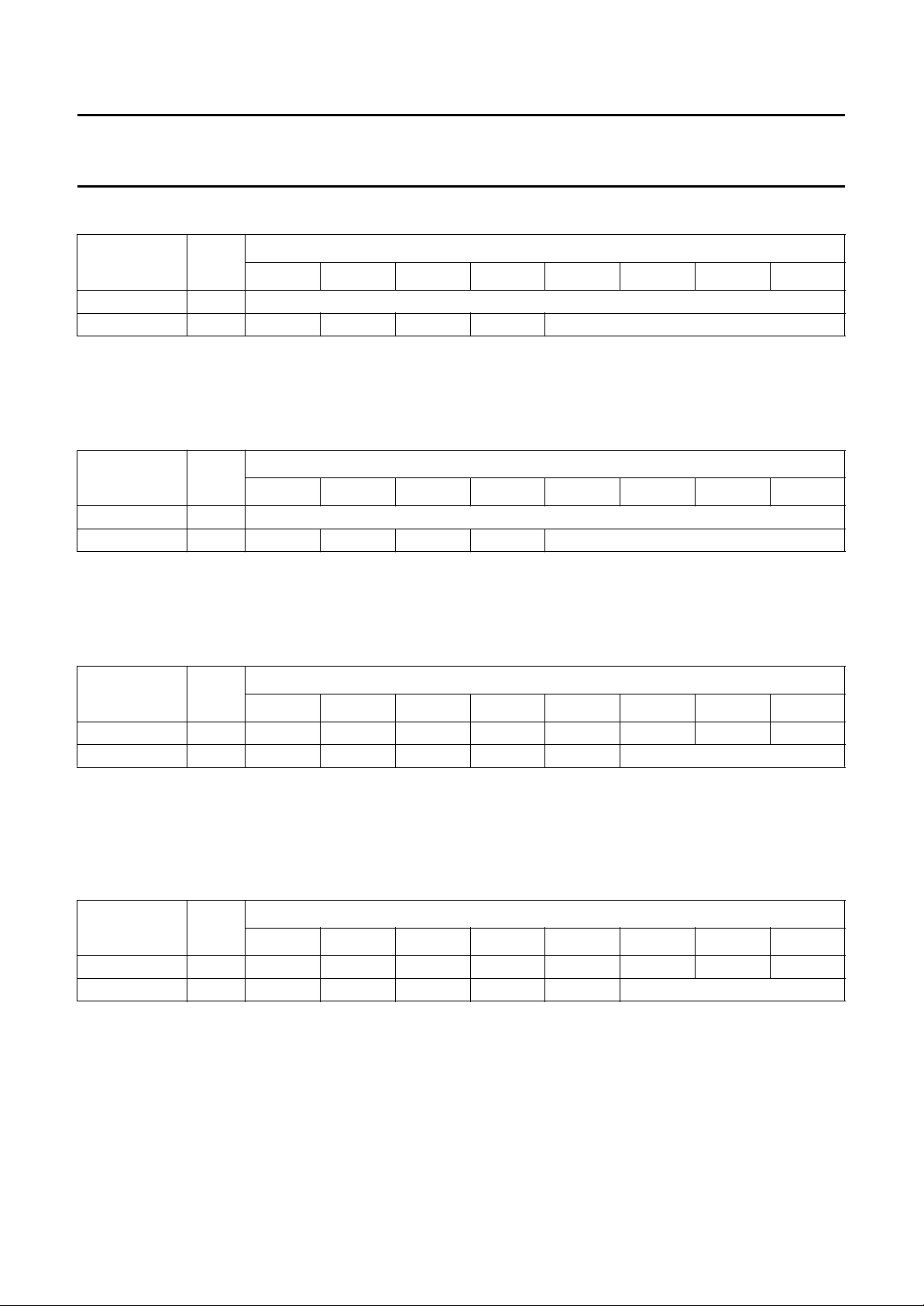
Philips Semiconductors Preliminary specification
High performance Compact
SAA7390
Disc-Recordable (CD-R) controller
Table 53 Host interface offset start register (A and B): 0xF0E8, F0E9; note 1
MNEMONIC R/W
76543210
HOSTOFFS R/W OFFSET7 to OFFSET0
HOSTOFFS R/W −−−− OFFSET11 to OFFSET8
Note
1. These registers, together with the offset end registers, allow full control over the number of frame bytes that will be
transferred to the host interface port.
Table 54 Host interface offset end register (A and B): 0xF0EA, F0EB; note 1
MNEMONIC R/W
76543210
HOSTOFFE R/W OFFSET7 to OFFSET0
HOSTOFFE R/W −−−− OFFSET11 to OFFSET8
Note
1. These registers together with the offset start registers, allow full control over the number of frame bytes that will be
transferred to the host interface port.
DATA BYTE
DATA BYTE
Table 55 Host interface transfer start frame number: 0xF0EC, F0ED; note 1
MNEMONIC R/W
76543210
HOSTSFRM R/W FRAME7 FRAME6 FRAME5 FRAME4 FRAME3 FRAME2 FRAME1 FRAME0
HOSTSFRM R/W −−−−− FRAME10 to FRAME8
Note
1. This register determines the starting frame number for a host interface transfer. The outputs of the registers are used
to directly control DRAM access cycles, and will affect any current DRAM cycle in progress. The host interface frame
pointer will wrap back to this point.
Table 56 Host interface current transfer frame: 0xF0EE, F0EF; note 1
MNEMONIC R/W
76543210
HOSTCFRM R FRAME7 FRAME6 FRAME5 FRAME4 FRAME3 FRAME2 FRAME1 FRAME0
HOSTCFRM R −−−−− FRAME10 to FRAME8
Note
1. This register allows the current host interface frame transfer number to be read.
DATA BYTE
DATA BYTE
1996 Jul 02 39
Page 40
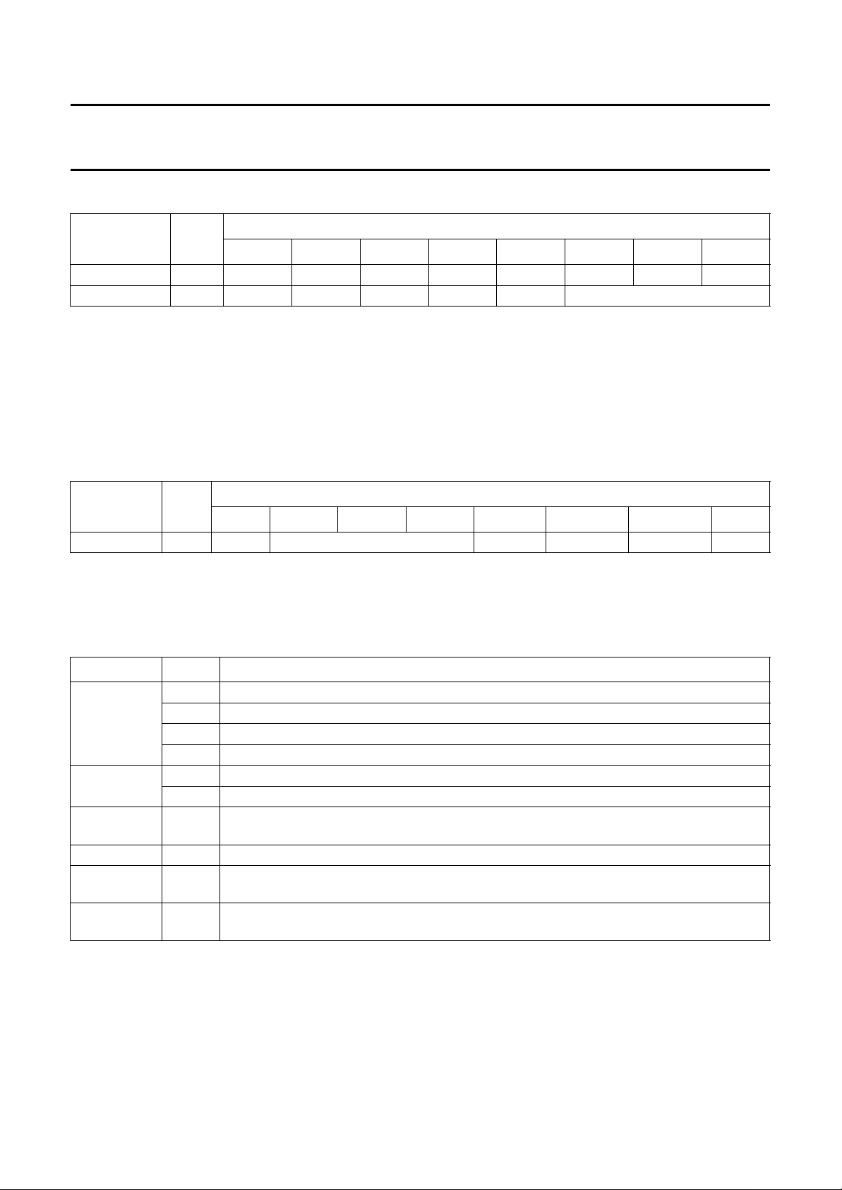
Philips Semiconductors Preliminary specification
High performance Compact
SAA7390
Disc-Recordable (CD-R) controller
Table 57 Ending frame number: 0xF0F2, F0F3
MNEMONIC R/W
76543210
LSTFHOST R/W FRAME7 FRAME6 FRAME5 FRAME4 FRAME3 FRAME2 FRAME1 FRAME0
LSTFHOST R/W −−−−− FRAME10 to FRAME8
11.5 Miscellaneous buffer manager considerations
The following bandwidth limitation must be observed in normal operation:
• Only 833 ns is available between each data write from the front-end at the maximum 8 times transfer rate. At the end
of the frame, multiple front-end writes may stack up, so the microcontroller accesses to DRAM will be off
(PCLK stopped) during the end of frame time.
• After power-up or reset, the register DRAMSEL should be programmed first.
Table 58 Selection/test mode: 0xF0FE; note 1
MNEMONIC R/W
76543 2 1 0
DRAMSEL R/W TEST RES_TEST2 to RES_TEST0 REFRATE DRAMSEL1 DRAMSEL0 −
DATA BYTE
DATA BYTE
Note
1. DRAMSEL1 and DRAMSEL0 are used to select the type of DRAM which is connected to the SAA7390. The test
modes are also defined by the DRAMSEL register.
Table 59 DRAMSEL field descriptions
FIELD LOGIC DESCRIPTION
DRAMSEL1
DRAMSEL0
REFRATE 0 normal refresh rate
RES_TEST0 − reserved for test; setting this HIGH enables the DRAM access test, a write to INTRMSK sets
RES_TEST1 − reserved for test; setting this HIGH enables the switch multiplexer control
RES_TEST2 − reserved for test; setting this HIGH enables the interrupt test, a write to PAGEREG will set
TEST − test mode; this bit must be set to enable the test modes, also, read back of any of the test
00 256 kbytes
01 1 Mbyte
10 not applicable
11 4 Mbytes
1
1 double refresh rate; set HIGH if clock is running at
a front-end access test, and a write to PAGEREG sets a test ECC access
interrupts
bits is gated by this bit
⁄2 normal rate, or 16.9 MHz
1996 Jul 02 40
Page 41
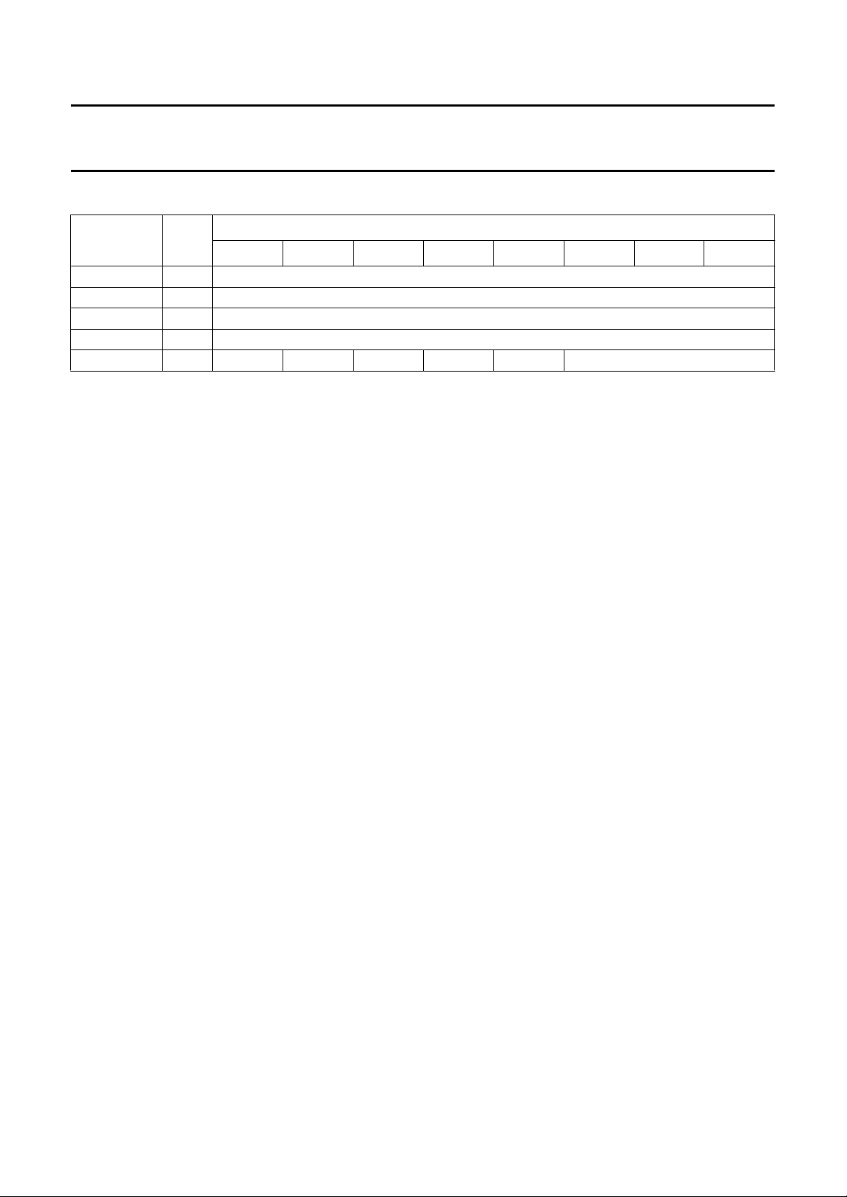
Philips Semiconductors Preliminary specification
High performance Compact
SAA7390
Disc-Recordable (CD-R) controller
Table 60 Automatic start and stop control functions (same address): 0xF0C5, F0C6 and F0C7
MNEMONIC R/W
76543210
STRTMIN R/W MINUTE7 to MINUTE0
STRTSEC R/W SECOND7 to SECOND0
STRTFRM R/W FRAME7 to FRAME0
STOPCNT R/W COUNT7 to COUNT0
STOPCNT R/W −−−−− COUNT10 to COUNT8
The multiplexing between the start and stop registers is
achieved by programming STOP in BMFECTL. If STOP is
clear then STRTMIN, STRTSEC and STRTFRM are
accessible, otherwise STOPCNT may be accessed.
These registers contain the start address (MSF) and the
stop count for the automatic read control function. When
the block decoders header or registers equal the start
address, the front-end will start to send data to the buffer
manager until the down counter STOPCNT decrements to
zero, at which time the data flow stops.
DATA BYTE
In the 53CF9X series of SCSI controllers, some registers
are read only and others are write only. These share the
same address and the multiplexing between the two
depends on the read or write select.
The address mapping is: 0xF0A4 to 0xF0A7,
0xF0AC to 0xF0AF, 0xF0B4 to 0xF0B7,
0xF0BC to 0xF0BF maps onto the external interface
device address range 0x00 to 0x0F respectively.
11.7 CDB2 related registers
The header registers are selected then AUDMODE in
FECTL is LOW, otherwise the Q registers are selected;
the latter event is used for loading audio data. The start
registers are selected when FEWBLK in BMFECLT is
LOW, otherwise the STOPCNT registers are selected. The
start registers should be programmed to ‘Header 1’. If
EFAB (C2 failure) is asserted while the header is shifting
in, the data flow will not start. The same is true for BADQ
(Q channel CRC failure) used in the audio mode.
11.6 Host interface related registers
The SAA7390 provides a 16 address wide pass through
mechanism to communicate to an external SCSI or ATAPI
interface device. Supported devices include the 53CF9X
series of SCSI controllers and the Wapiti ATAPI controller.
The register definitions for the external device can be
found in the corresponding data sheet.
This section outlines the registers which are related to the
modified CDB2 block encoder. Figure 13 shows a
functional block diagram for the CDB2.
Figure 14 explains the generation of header and
sub-header information.
1996 Jul 02 41
Page 42
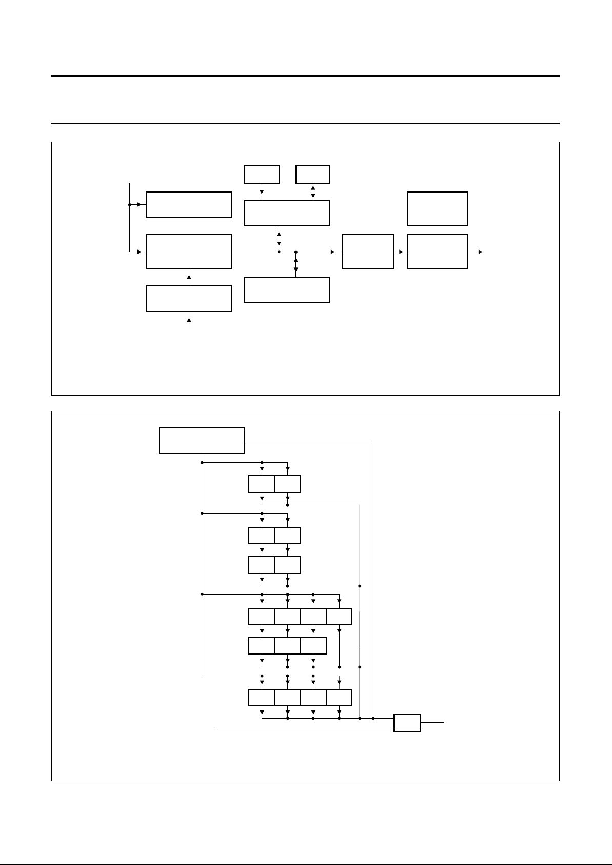
Philips Semiconductors Preliminary specification
High performance Compact
Disc-Recordable (CD-R) controller
handbook, full pagewidth
microcontroller
access
MICROCONTROLLER
INTERFACE
BLOCK COUNTER
AND
HEADER GENERATION
DATA
INTERFACE
data cource
Fig.13 Functional block diagram for the CDB2.
ROM RAM
ERROR CORRECTION
CODE GENERATION
ERROR DETECTION
CODE GENERATION
SCRAMBLER
TIMER AND
CONTROL
LOGIC
BYTE SWAP
AND
2
S INTERFACE
I
SAA7390
I2S output
MGD620
handbook, full pagewidth
MICROCONTROLLER
INTERFACE
registers
registers
registers
registers
registers
registers
data
CMD
STS
BCH BCL
BCH BCL
MIN SEC
MIN SEC
FILN CHAN SUBM DTYP
FRM MODE
FRM
BCM
MUX
output
MGD621
Fig.14 Generation of the header and sub-header information.
1996 Jul 02 42
Page 43
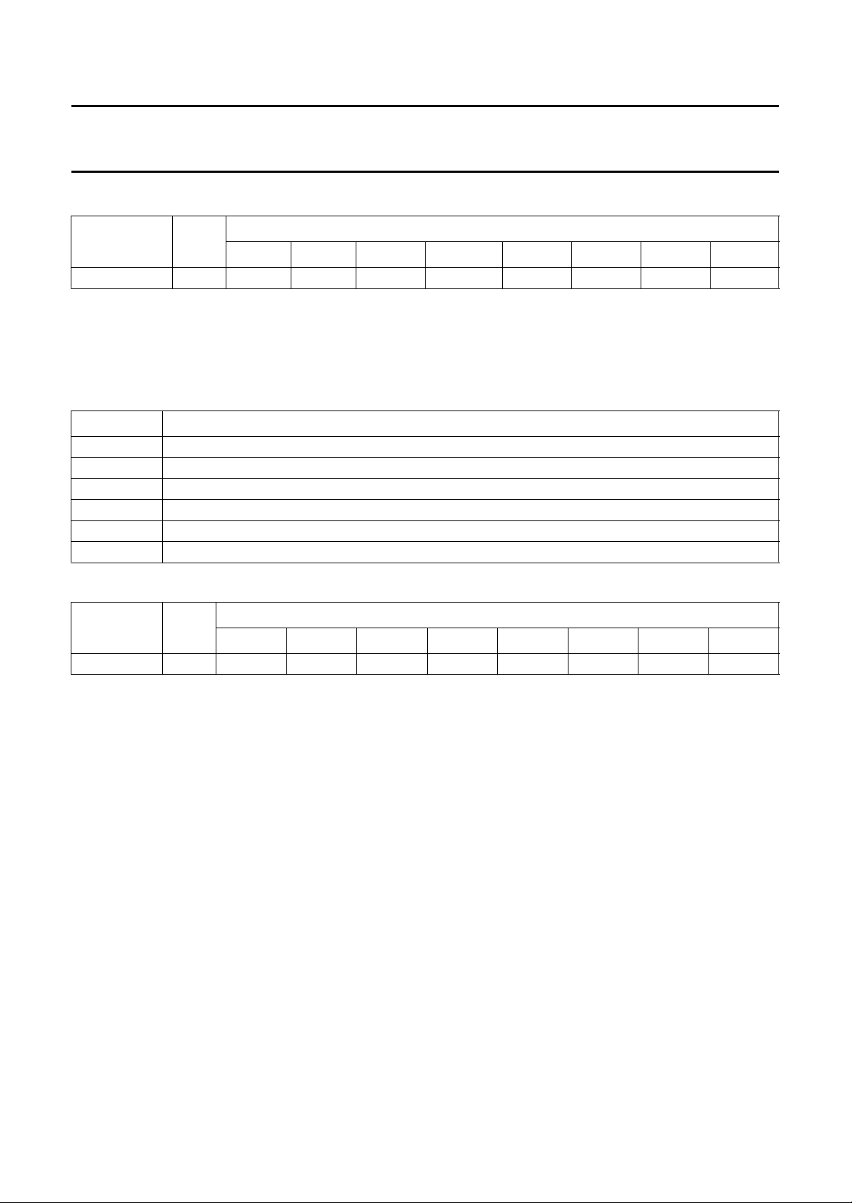
Philips Semiconductors Preliminary specification
High performance Compact
SAA7390
Disc-Recordable (CD-R) controller
Table 61 Interrupt mask register: 0xF0CE; note 1
MNEMONIC R/W
765 4 3210
CMSK R/W −−EOFMSK COM_SYS ACKINT HEF ACA LBT
Note
1. Register 0xF0CE contains the mask bits for the various SAA7390 specific interrupts. Setting a mask bit HIGH
enables the interrupt. The register is cleared to all zeros after reset. The definitions of the bit fields of CMSK are given
in Table .63.
Table 62 CMSK field descriptions
FIELD DESCRIPTION
LBT block counter equals zero
ACA access allowed
HEF DMA to CDB2 under-run
ACKINT interrupt from serial communication with basic engine
COM_SYS COMSYNC/SYSSYNC clock interrupt
EOFMSK end of frame interrupt generated by CDB2 when writing to the disc in audio or data mode
DATA BYTE
Table 63 Command register: 0xF0D1
MNEMONIC R/W
76543210
CCMD R/W SRS BPE ACT DRQ NHD CDI SBH ED2
DATA BYTE
1996 Jul 02 43
Page 44
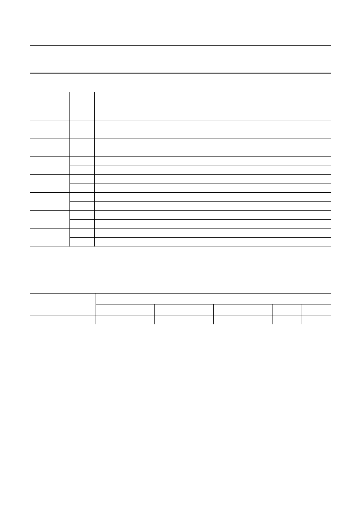
Philips Semiconductors Preliminary specification
High performance Compact
Disc-Recordable (CD-R) controller
Table 64 CCMD field descriptions
FIELD LOGIC DESCRIPTION
ED2 0 no EDC in CDI, Form 2; zeros replace CRC; note 1
1 EDC is performed in CDI, Form 2; note 1
SBH 0 sub-header retrieved from sub-header register; note 2
1 sub-header retrieved from host data; note 2
CDI 0 CD-ROM mode; note 2
1 CDI mode; note 2
NHD 0 header calculated internally; note 2
1 header supplied by host; note 2
DRQ 0 requests to host are enabled; note 2
1 requests to host are disabled; this is now synchronous with the end-of-frame signal; note 2
ACT 0 continue transmission; note 2
1 stop transmission during next block; note 2
BPE 0 bypass disabled; note 2
1 bypass enabled; this is now synchronous with the end-of-frame signal; note 2
SRS 0 normal operation
1 soft reset to CDB2
SAA7390
Notes
1. Only has effect in CDI mode.
2. Latched on rising edge of ACA.
Table 65 Status register: 0xF0D2
MNEMONIC R/W
76543210
CSTS R ATT HEF LBT ACA RDY NRQ SAR −
DATA BYTE
1996 Jul 02 44
Page 45
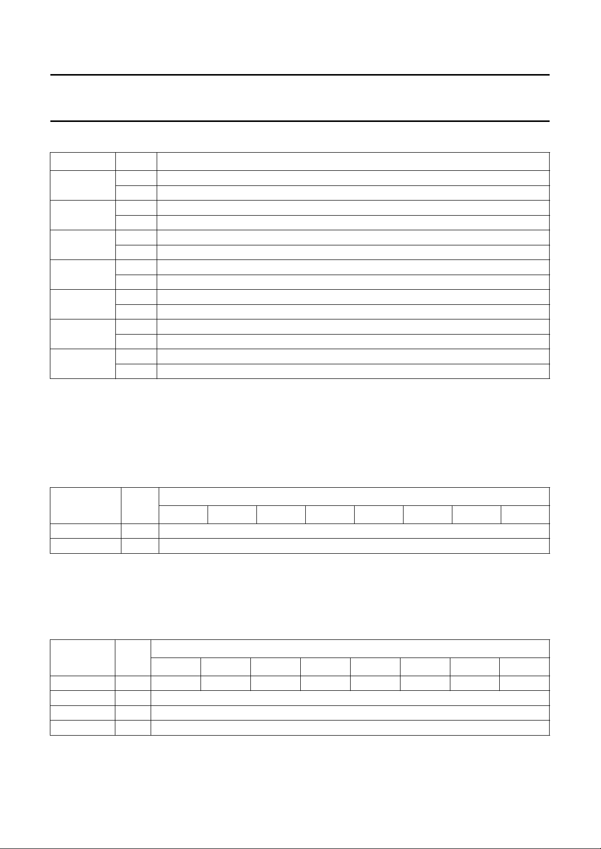
Philips Semiconductors Preliminary specification
High performance Compact
Disc-Recordable (CD-R) controller
Table 66 CSTS field descriptions
FIELD LOGIC DESCRIPTION
SAR 0 status not ready yet during this block; SAR cleared on each new block
1 status already read
(1)
NRQ
(2)
RDY
ACA 0 access to CDB2 is denied
LBT 0 state of block counter has reached zero
HEF 0 no error has occurred during communication with the host
(4)
ATT
0 no request to host will be issued
1 requests to host will be issued
0 data block transmission is in progress
1 data transmission is ceased
1 access to CDB2 is allowed
1 block counter is non zero
1 an error has occurred in the host communication process; note 3
0 interrupt to microcontroller is asserted
1 no pending interrupts
SAA7390
Notes
1. Normally NRQ is LOW during synchronization, header and EDC/ECC transmission.
2. RDY is set after command bit ACT is pulled LOW.
3. This is a fatal error which can be rectified only by restarting CDB2.
4. Interrupt sources are ACA = logic 1, LBT = logic 0 and HEF = logic 1.
Table 67 Block count registers: 0xF0D3 and 0xF0D4; note 1
MNEMONIC R/W
76543210
CBCL R/W BLOCKCOUNT7 to BLOCKCOUNT0
CBCH R/W BLOCKCOUNT15 to BLOCKCOUNT8
Note
1. This is a 16-bit down counter which should be programmed with the; number of blocks - 1. As soon as the count value
reaches zero, LBT is cleared and ATT is pulled LOW. LBT remains active for 13.3 ms at single speed record. Note
that the counter continue to decrement. New programmed information is used at the start of the next block.
Table 68 Header containing MSF address and mode: 0xF0D5, F0D6, F0D7 and F0DB
MNEMONIC R/W
76543210
CMDE R/W −−−−−−MODE1 MODE0
CMIN R/W MINUTES7 to MINUTES0
CSEC R/W SECONDS7 to SECONDS0
CFRM R/W FRAME7 to FRAME0
DATA BYTE
DATA BYTE
1996 Jul 02 45
Page 46
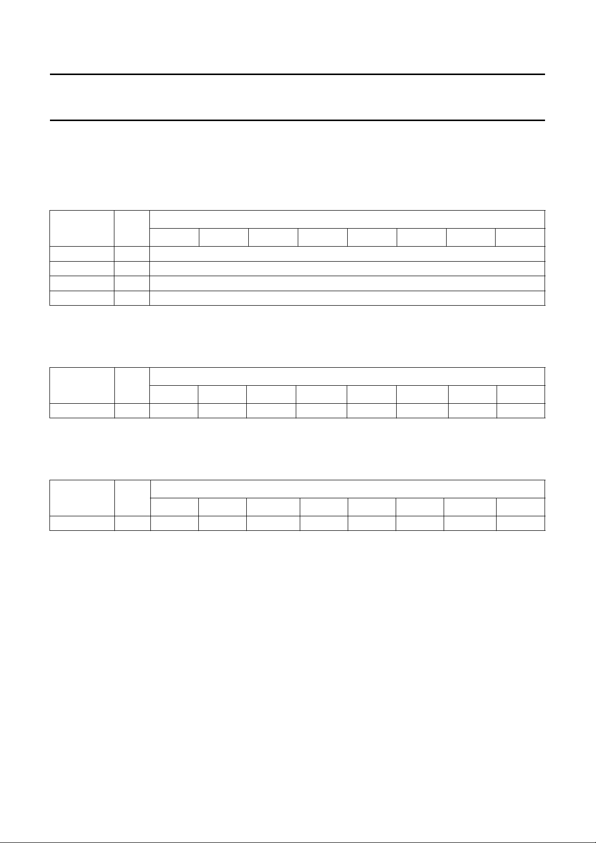
Philips Semiconductors Preliminary specification
High performance Compact
SAA7390
Disc-Recordable (CD-R) controller
Automatic header generation is implemented in the CDB2. Once the initial header value is loaded, the header is
incremented and added to the user data in accordance with the Yellow book rules. When the information is written into
the header registers, this is used by the CDB2 at the start of the next frame. MODE1 and MODE0 specifies the CD-ROM
mode used, even when NHD = logic 1.
Table 69 Sub-header information fields: 0xF0DC, F0DD, F0DE and F0DF; note 1
MNEMONIC R/W
76543210
CFN R/W FILENUMBER7 to FILENUMBER0
CCHAN R/W CHANNEL7 to CHANNEL0
CSMD R/W SUBMODE7 to SUBMODE0
CDTB R/W DATATYPE7 to DATATYPE0
Note
1. These form the CDB2 sub-header information, comprising of the file number, channel, mode and data type.
Table 70 Test register for CDB2: 0xF0D8; note 1
MNEMONIC R/W
765 4 3 2 10
CTST W −−SYN_PD S_CPSEL S_FDBK S_OUTEN TEST1 TEST0
DATA BYTE
DATA BYTE
Note
1. This register is strictly for use by the manufacturer. Setting any bits will result in undefined operation.
Table 71 Control register for CDB2: 0xF0D9
MNEMONIC R/W
76 5 432 1 0
CCTL R/W HSTSH HSH CDB2ECC −−− 0 RSTA
DATA BYTE
1996 Jul 02 46
Page 47
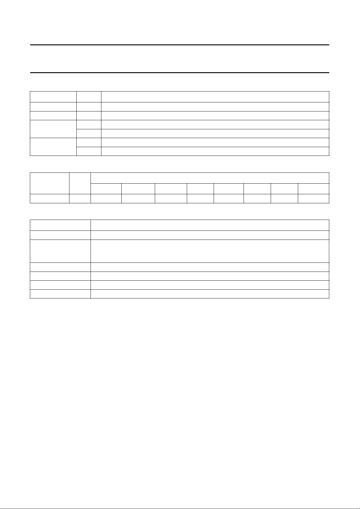
Philips Semiconductors Preliminary specification
High performance Compact
SAA7390
Disc-Recordable (CD-R) controller
Table 72 CCTL field descriptions
FIELD LOGIC DESCRIPTION
RSTA to reset CDB2, first set RSTA HIGH then LOW
CDB2ECC when set, enables the ECC RAM to be used by the CDB2 during encoding of ECC parity
(1)
HSH
HSTSH
Table 73 Status register for CDB2: 0xF0DA
Table 74 CCTL field descriptions
EOFCDB2 end of frame interrupt from CDB2; generated in both bypass and CD-ROM modes
COMACK Acknowledge signal from the basic engine indicating reception of a byte in its register. The
ACKINT indicates a HIGH-to-LOW transition on COMACK; this status is not affected by masking bits
SYSSYNC one of the serial synchronization signals
COMSYNC one of the serial synchronization signals
COM/SYS combination of the SYSSYNC and COMSYNC interrupts; control of selection is via SC_CTL
(2)
MNEMONIC R/W
CSTAT R COM/SYS COMSYNC SYSSYNC ACKINT COMACK −−EOFCDB2
FIELD DESCRIPTION
0 header supplied from CDB2
1 header supplied by host
0 sub-header supplied from CDB2
1 sub-header supplied by host
DATA BYTE
7 6 5 43210
HIGH-to-LOW transition of this signal indicates ‘ready to receive’ and generates an interrupt
to the microcontroller.
1996 Jul 02 47
Page 48
Philips Semiconductors Preliminary specification
High performance Compact
Disc-Recordable (CD-R) controller
12 FRAME BUFFER ORGANIZATION
The break-down of the 3 kbytes frame buffer is described in this section.
Table 75 Frame buffer organization
DECIMAL HEXADECIMAL
START END LEN START END LEN
0 11 12 000 00B 00C synchronization field
12 15 4 00C 00F 004 header
16 2063 2048 010 80F 800 frame data
2064 2067 4 810 813 004 CRC parity
2068 2075 8 814 81B 008 padding
2076 2247 172 81C 8C7 0AC P parity
2248 2351 104 8C8 92F 068 Q parity
2352 2367 16 930 93F 010 Q channel
2368 2463 96 940 99F 060 sub-channel
2464 2757 294 9A0 AC5 126 error flags
2758 2761 4 AC6 AC9 004 CRC remainder
2762 2933 172 ACA B75 0AC P syndromes
2934 3037 104 B76 BDD 068 Q syndromes
3038 3038 1 BDE BDE 001 status
SAA7390
DATA
Table 76 ECC RAM organization
DEC HEX
3210
000 000 psyn[00].s1 psyn[00].s0 qsyn[00].s1 qsyn[00].s0
↓↓↓↓↓↓
204 0CC psyn[51].s1 psyn[51].s0 qsyn[51].s1 qsyn[51].s0
208 0D0 psyn[52].s1 psyn[52].s0 flags[001] flags[000]
↓↓↓↓↓↓
340 154 psyn[85].s1 psyn[85].s0 flags[067] flags[066]
344 158 flags[071] flage[070] flags[069] flags[068]
↓↓↓↓↓↓
564 234 flags[291] flage[290] flags[289] flags[288]
568 238 unused[1] unused[0] flags[293] flags[292]
572 23C crc_rem[3] crc_rem[2] crc_rem[1] crc_rem[0]
576 240 header[3] header[2] header[1] header[0]
580 244 ecc_reg[03] ecc_reg[02] ecc_reg[01] ecc_reg[00]
584 248 ecc_reg[07] ecc_reg[06] ecc_reg[05] ecc_reg[04]
588 588 ecc_reg[11] ecc_reg[10] ecc_reg[09] ecc_reg[08]
BYTE NUMBER
1996 Jul 02 48
Page 49

Philips Semiconductors Preliminary specification
High performance Compact
Disc-Recordable (CD-R) controller
13 SUMMARY OF CONTROL REGISTER MAP Table 77 Control register map for the SAA7390
ADDRESS MNEMONIC READ/WRITE DESCRIPTION
F084 QZERO R Q channel zero byte
F085 ECCCTL R/W ECC control register
F086 ECCSTAT R ECC status register
F08E NUM_COR R ECC register for the number of corrections
F08F TDB_CNT R/W track descriptor count
F091 CLKSEL W start the clock synthesizer (doubler)
F092 HDRMODE R header mode byte from block decoder
F093 HDRFRM R header frame byte from block decoder
F094 QFRM R Q channel frame (track relative)
F095 QMIN R Q channel minutes (track relative)
F096 TDB R/W track descriptor block frame number low
F097 TDB R/W track descriptor block frame number high
F09A HDRSEC R header seconds byte from block decoder
F09B HDRMIN R header minutes byte from block decoder
F09C HOFF R host interface offset register low
F09D HOFF R host interface offset register high
F09E FEOFF R front-end offset register low
F09F FEOFF R front-end offset register high
F0A1 WTS2B W S2B UART transmit buffer
F0A2 RDS2B R S2B UART receive buffer
F0A3 S2BSTAT R S2B UART status register
F0A4 HOSTPASS R/W interface device pass through register address 0x00
F0A5 HOSTPASS R/W interface device pass through register address 0x01
F0A6 HOSTPASS R/W interface device pass through register address 0x02
F0A7 HOSTPASS R/W interface device pass through register address 0x03
F0A9 QTNO R Q channel track number
F0AA QMODE R Q channel mode number
F0AB QAMIN R Q channel minutes number (absolute)
F0AC HOSTPASS R/W interface device pass through register address 0x04
F0AD HOSTPASS R/W interface device pass through register address 0x05
F0AE HOSTPASS R/W interface device pass through register address 0x06
F0AF HOSTPASS R/W interface device pass through register address 0x07
F0B1 QASEC R Q channel seconds (absolute)
F0B2 QAFRM R Q channel frames (absolute)
F0B3 −−not connected
F0B4 HOSTPASS R/W interface device pass through register address 0x08
F0B5 HOSTPASS R/W interface device pass through register address 0x09
F0B6 HOSTPASS R/W interface device pass through register address 0x0A
SAA7390
1996 Jul 02 49
Page 50

Philips Semiconductors Preliminary specification
High performance Compact
Disc-Recordable (CD-R) controller
ADDRESS MNEMONIC READ/WRITE DESCRIPTION
F0B7 HOSTPASS R/W interface device pass through register address 0x0B
F0B9 WTGCTL W GLIC control registers (audio control)
F0BA RDSW R drive control switches register
F0BB FECTL R/W front-end control register
F0BC HOSTPASS R/W interface device pass through register address 0x0C
F0BD HOSTPASS R/W interface device pass through register address 0x0D
F0BE HOSTPASS R/W interface device pass through register address 0x0E
F0BF HOSTPASS R/W interface device pass through register address 0x0F
F0C0 BRGSEL R/W baud rate generator select register
F0C1 WTDIR R/W SAA7390-host interface direction plus audio mode control
F0C2 GPIOCTL R/W general purpose bits control register
F0C3 RDDSTAT R data status register
F0C4 SERCOM R/W SAA7390: basic engine communications port
F0C5 STRTMIN R/W start minutes (automatic control)
F0C6 STRTSEC R/W start seconds (automatic control)
F0C6 STOPCNT R/W stop count low byte (automatic control)
F0C7 STRTFRM R/W start frame (automatic control)
F0C7 STOPCNT R/W stop count high byte (automatic control)
F0C9 RDJMPRS R option jumper register (attached to DRAM data bus)
F0CE CMSK R/W CDB2 interrupt mask register
F0CF QINDX R Q channel index (track relative)
F0D1 CCMD R/W CDB2 command register
F0D2 CSTS R CDB2 status register
F0D3 CBCH R/W CDB2 block counter high
F0D4 CBCL R/W CDB2 block counter low
F0D5 CMIN R/W CDB2 header minutes register
F0D6 CSEC R/W CDB2 header seconds register
F0D7 CFRM R/W CDB2 header frame register
F0D8 CTST W test register for CDB2 block
F0D9 CCTL R/W control register for CDB2 block
F0DA CSTAT R status register for CDB2 block
F0DB CMDE R/W CDB2 header mode register
F0DC CFN R/W CDB2 file number register
F0DD CCHAN R/W CDB2 channel number register
F0DE CSMD R/W CDB2 sub-mode byte register
F0DF CDTB R/W CDB2 data type byte register
F0E1 BMFECTL R/W buffer manager front-end control
F0E2 FEFRMOFF R/W front-end 8 LSBs; frame offset
F0E3 FEFRMOFF R/W front-end 4 MSBs; frame offset (bit 0 to bit 3)
F0E4 FEFRM# R/W front-end 8 LSBs of the frame
F0E5 FEFRM# R/W front-end 3 MSBs of the frame (bit 0 to bit 2)
SAA7390
1996 Jul 02 50
Page 51

Philips Semiconductors Preliminary specification
High performance Compact
SAA7390
Disc-Recordable (CD-R) controller
ADDRESS MNEMONIC READ/WRITE DESCRIPTION
F0E6 LSTCMPFM R 8 LSBs; last complete frame number
F0E7 LSTCMPFM R 3 MSBs; last complete frame number (bit 0 to bit 2)
F0E8 HOSTOFFS R/W host interface 8 LSBs; offset start (A and B)
F0E9 HOSTOFFS R/W host interface 4 MSBs; offset start (bit 0 to bit 3)
F0EA HOSTOFFE R/W host interface 8 LSBs; offset end (A and B)
F0EB HOSTOFFE R/W host interface 4 MSBs; offset end (bit 0 to bit 3)
F0EC HOSTSFRM R/W host interface 8 LSBs; start transfer frame number
F0ED HOSTSFRM R/W host interface 3 MSBs; start frame number (bit 0 to bit 2)
F0EE HOSTCFRM R/W host interface 8 LSBs; current frame number
F0EF HOSTCFRM R/W host interface 3 MSBs; current frame number (bit 0 to bit 2)
F0F1 SC_CTL R/W serial communication control
F0F2 LSTFHOST R/W last frame host interface LOW
F0F3 LSTFHOST R/W last frame host interface HIGH
F0F4 ECCFRM# R/W ECC 8 LSBs; frame number (frame address)
F0F5 ECCFRM# R/W ECC 3 MSBs; frame number (bit 0 to bit 2)
F0F6 MICFRM# R/W microcontroller 8 LSBs; frame number (frame address)
F0F7 MICFRM# R/W microcontroller 3 MSBs; frame number (bit 0 to bit 2)
F0F8 LASTFRM R/W last frame number for storage 8 LSBs
F0F9 LASTFRM R/W last frame number 3 MSBs (bit 0 to bit 2)
F0FA QSEC R Q channel seconds (track relative)
F0FB INTRMSK R/W interrupt mask register
F0FC INTRFLG R/W interrupt flag register
F0FD HOSTMOD R/W host interface mode control
F0FE DRAMSEL R/W DRAM selection/test mode register.
F0FF PAGEREG R/W 80C32 linear address page register
1996 Jul 02 51
Page 52
Philips Semiconductors Preliminary specification
High performance Compact
SAA7390
Disc-Recordable (CD-R) controller
14 LIMITING VALUES
In accordance with the Absolute Maximum Rating System (IEC 134).
SYMBOL PARAMETER MIN. MAX. UNIT
V
DD
V
i(max)
V
o
T
stg
15 OPERATING CHARACTERISTICS
15.1 I
= 4.75 to 5.25 V; VSS=0V; T
V
DD
SYMBOL PARAMETER CONDITIONS MIN. TYP. MAX. UNIT
2
I
S-bus timing (single speed × n); see Fig.15 and note 1
CLOCK INPUT: CLAB
T
cy
t
CH
t
CL
INPUTS: DAAB, WSAB AND EFAB
t
su
t
h
digital supply voltage −0.5 +7 V
maximum input voltage on any pin VSS− 0.5 VDD+ 0.5 V
output voltage on any output −0.5 +7 V
storage temperature −55 +150 °C
2
S-bus timing; data mode
= −10 to +70 °C; unless otherwise specified.
amb
output clock period sample rate = f
sample rate = 2 f
sample rate = 4 f
clock HIGH time sample rate = f
sample rate = 2f
sample rate = 4f
clock LOW time sample rate = f
sample rate = 2f
sample rate = 4f
set-up time sample rate = f
sample rate = 2f
sample rate = 4f
hold time sample rate = f
sample rate = 2f
sample rate = 4f
s
s
s
s
s
s
s
s
s
s
s
s
s
− 472.4/n − ns
− 236.2/n − ns
s
− 118.1/n − ns
s
166/n −−ns
83/n −−ns
42/n −−ns
166/n −−ns
83/n −−ns
42/n −−ns
95/n −−ns
48/n −−ns
24/n −−ns
95/n −−ns
48/n −−ns
24/n −−ns
Note
1. The I
2
S-bus timing is directly related to the overspeed factor ‘n’ in the normal operating mode. In the lock-to-disc
mode ‘n’ is replaced by the disc speed factor ‘d’.
1996 Jul 02 52
Page 53
Philips Semiconductors Preliminary specification
High performance Compact
SAA7390
Disc-Recordable (CD-R) controller
15.2 EIAJ timing; audio mode
V
= 4.75 to 5.25 V; VSS=0V; T
DD
SYMBOL PARAMETER CONDITIONS MIN. TYP. MAX. UNIT
EIAJ timing (single speed × n); see Fig.16 and note 1
C
LOCK INPUT: CLAB
T
cy
t
CH
t
CL
output clock period sample rate = f
clock HIGH time sample rate = f
clock LOW time sample rate = f
INPUTS: DAAB, WSAB AND EFAB
t
su
t
h
set-up time sample rate = f
hold time sample rate = f
= −10 to +70 °C; unless otherwise specified.
amb
− 472.4/n − ns
− 236.2/n − ns
s
− 118.1/n − ns
s
166/n −−ns
83/n −−ns
42/n −−ns
166/n −−ns
83/n −−ns
42/n −−ns
95/n −−ns
48/n −−ns
24/n −−ns
95/n −−ns
48/n −−ns
24/n −−ns
sample rate = 2 f
sample rate = 4 f
sample rate = 2f
sample rate = 4f
sample rate = 2f
sample rate = 4f
sample rate = 2f
sample rate = 4f
sample rate = 2f
sample rate = 4f
s
s
s
s
s
s
s
s
s
s
s
s
s
Note
1. The EIAJ timing is directly related to the overspeed factor ‘n’ in the normal operating mode. In the lock-to-disc mode
‘n’ is replaced by the disc speed factor ‘d’.
1996 Jul 02 53
Page 54
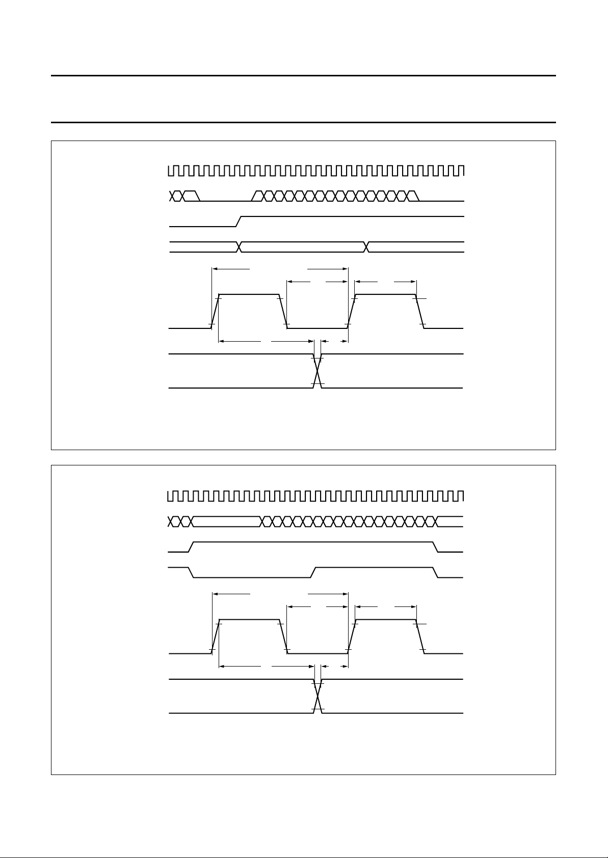
Philips Semiconductors Preliminary specification
High performance Compact
Disc-Recordable (CD-R) controller
handbook, full pagewidth
CLAB
DAAB
WSAB
EFAB
(error flags)
CLAB
DAAB
WSAB
EFAB
1
0
left
left LSB valid
15 14 13 12 11 10
clock period T
76543210
8
9
right
right MSB valid right LSB valid
cy
t
CL
t
h
t
su
VDD − 0.8 V
0.8 V
t
CH
V
DD
0.8 V
SAA7390
− 0.8V
MGE399
handbook, full pagewidth
CLAB
DAAB
WSAB
EFAB
CLAB
DAAB
WSAB
EFAB
10
Fig.15 I2S-bus timing diagram.
17
16 15 14 13 12 11 10 9 8 7 6 5 4 3 2 1 0
left
clock period T
t
h
cy
t
CL
t
VDD − 0.8 V
0.8 V
right
t
CH
V
− 0.8V
DD
0.8 V
su
MGE400
Fig.16 EIAJ timing diagram.
1996 Jul 02 54
Page 55
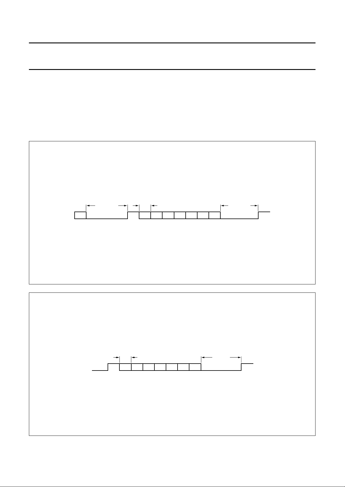
Philips Semiconductors Preliminary specification
High performance Compact
Disc-Recordable (CD-R) controller
15.3 R-W timing (see Fig.17)
The data from sub-code R-W may be read via the V4 pin
from the CD-decoder (SAA7372) and has a format similar
to RS232. The sub-code synchronization word is
formatted by a pause of 200 µs minimum. Each sub-code
byte starts with a logic 1 followed by seven bits (Q to W).
The gap between bytes is variable between 1.3 and 90 µs.
handbook, full pagewidth
200 µs min
W96
11.3
µs
1 Q1R1S1T1U1V1W1
SAA7390
15.4 C-flag timing (see Fig.18)
A 1-bit flag signal is input to the CFLAG pin. This signal
shows the status of the error corrector and interpolator and
is updated every frame.
11.3 µs min
90 µs max
1
MGE401
handbook, full pagewidth
Fig.17 Sub-code formatting and timing from the V4 pin.
11.3
µs
F1 F2 F3 F4 F5 F6 F7
45.4 µs
(nominal speed)
Fig.18 C-flag output timing.
MGE402
1996 Jul 02 55
Page 56
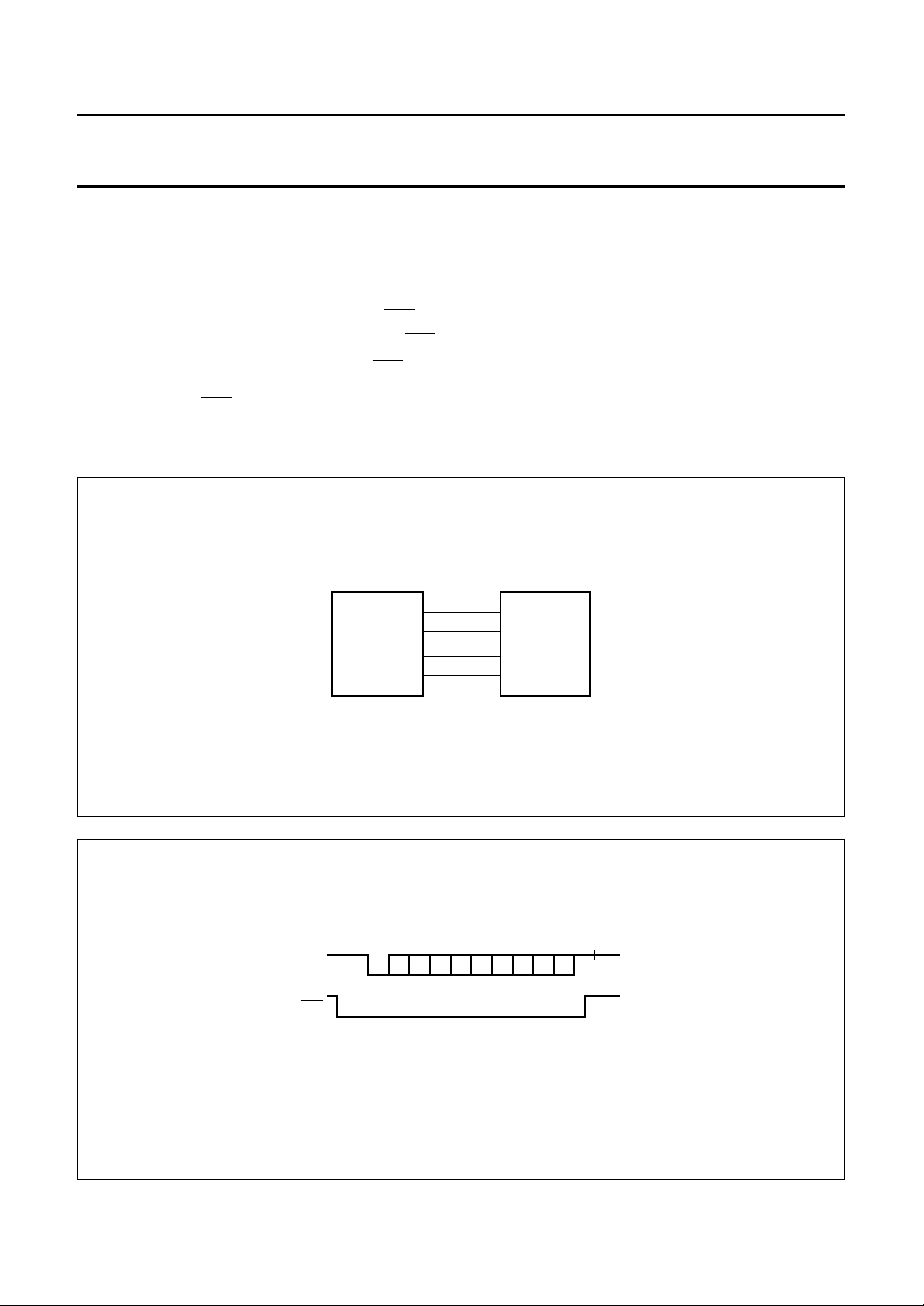
Philips Semiconductors Preliminary specification
High performance Compact
Disc-Recordable (CD-R) controller
15.5 S2B interface timing
The S2B serial interface consists of four lines (see Fig.19):
Transmit data (TXD)
Receive data (RXD)
Data path ready to accept data; active LOW (CPR)
Basic engine ready to accept data; active LOW (SPR).
These are used for communication. TXD and CPR for
sending acknowledges and information data to the data
path and RXD and SPR for receiving commands and
parameters from the data path. The data is transferred
frame-wise and asynchronously.
handbook, halfpage
data path
SAA7390
A data frame is proceeded by a start-bit (active LOW),
followed by the actual data byte, and again followed by a
parity bit (even parity), and a stop bit (active HIGH),
see Fig.20. In total, eleven bits per frame are incorporated.
The interface is full duplex, meaning data frames may be
transmitted and received simultaneously.
The bit-rate is selectable:
187.5 kbits/s with a 2.6% error
62.5 kbits/s with a 0.4% error
31.25 kbits/s with a 0.4% error.
basic engine
handbook, halfpage
CPR
RXD
CPR
TXD
SPR
sequoia
TXD
CPR
RXD
SPR
MGE403
Fig.19 S2B interface.
S0TXD 01234567PS1
MGE404
Fig.20 S2B Timing.
1996 Jul 02 56
Page 57
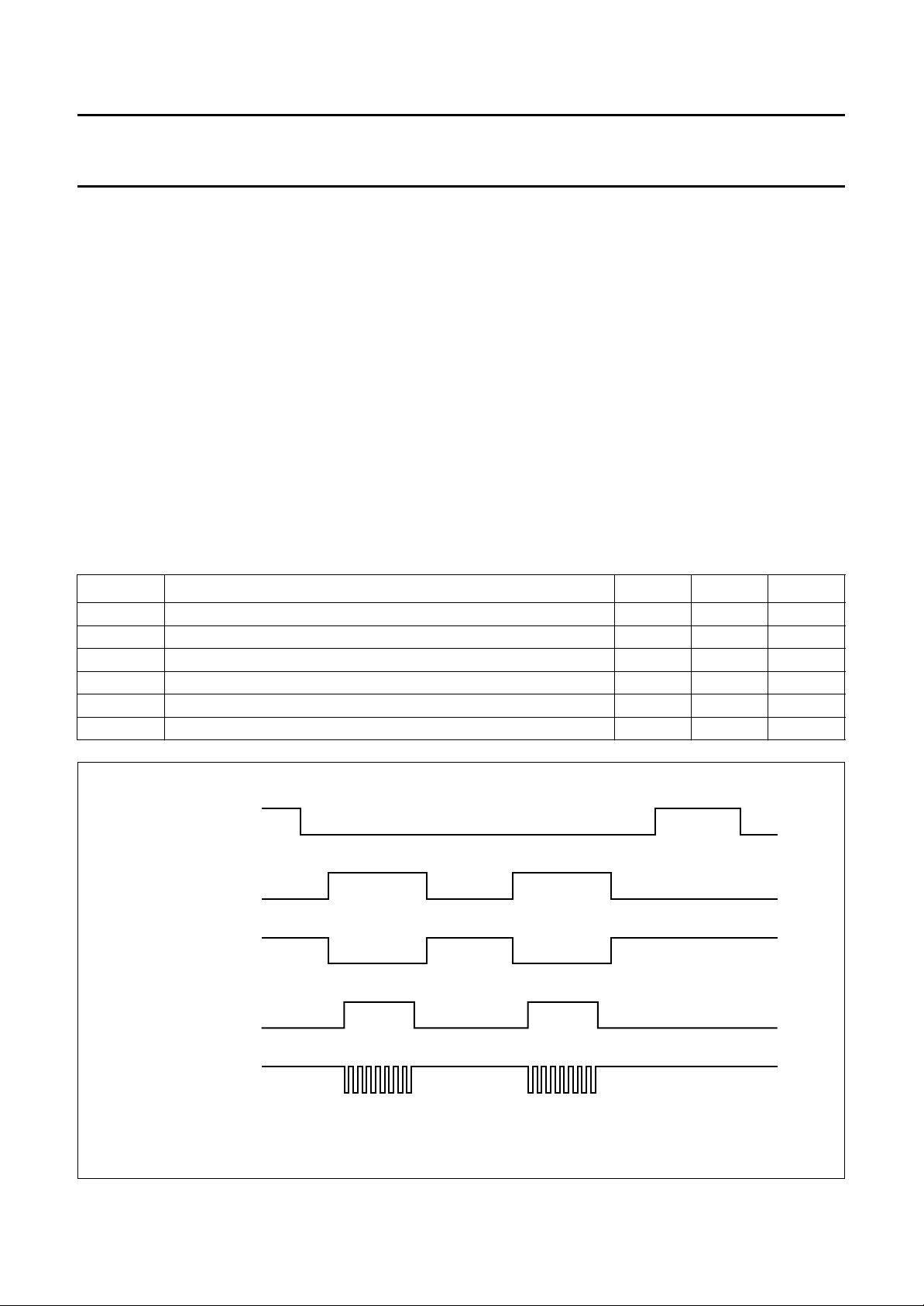
Philips Semiconductors Preliminary specification
High performance Compact
SAA7390
Disc-Recordable (CD-R) controller
15.6 SPI interface timing
The control communication between the CD-R engine and
the interface module is based on data blocks that are
swapped in the same cycle.
The control communication channel is byte and message
synchronous. Byte synchronization is realized with an
acknowledge after each byte that is transferred. Message
synchronization is ensured through resetting the serial
shift register after each communication synchronization
pulse. This is to detect the start of the next data block even
if a time-out or bit-slip occurs.
This control interface is used for the exchange of:
• Sub-code data
• Commands with parameters
• Status information.
Table 78 SPI timing parameters
SYMBOL PARAMETER MIN. MAX. UNIT
T
cy
t
CH
t
CL
t
su
t
h
t
d
serial clock cycle time 500 − ns
serial clock HIGH time 210 − ns
Serial clock LOW time 210 − ns
serial input data set-up time to COM_CLK 80 − ns
serial input data hold time from COM_CLK 80 − ns
serial output delay after COM_CLK 0 150 ns
The control interface channel is implemented as a
bidirectional, synchronous, high-speed serial link, having
the following advantages:
• The Q sub-code and header data can be coupled
(synchronized)
• The user part has real time access of the Q sub-code
information
• The user part has full control over the CD-R engines
mode of operation, for example synchronous stop while
recording
• High speed data transfers are possible; up to 2 Mbits/s
for the microcontroller in slave mode.
handbook, full pagewidth
COMM_SYNC
engine data available
COM_ACK
user data available
COM_CLK
Fig.21 Serial communication timing and synchronization.
1996 Jul 02 57
MGE523
Page 58
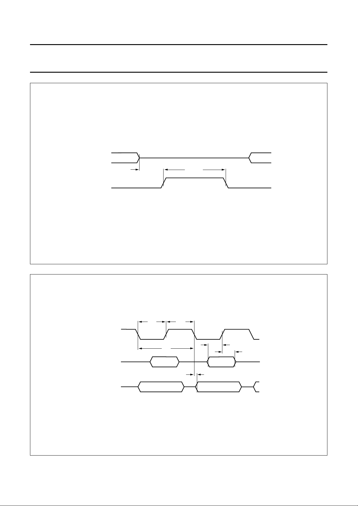
Philips Semiconductors Preliminary specification
High performance Compact
Disc-Recordable (CD-R) controller
handbook, full pagewidth
serial data in
acknowledge
30 to 700
µs
30 to 700
µs
SAA7390
MGE524
handbook, full pagewidth
COM_CLK
COM_IN
COM_OUT
Fig.22 Acknowledge signal timing.
t
CL
t
CH
t
T
cy
su
t
d
t
h
MGE525
Fig.23 Synchronous serial communication channel timing.
1996 Jul 02 58
Page 59
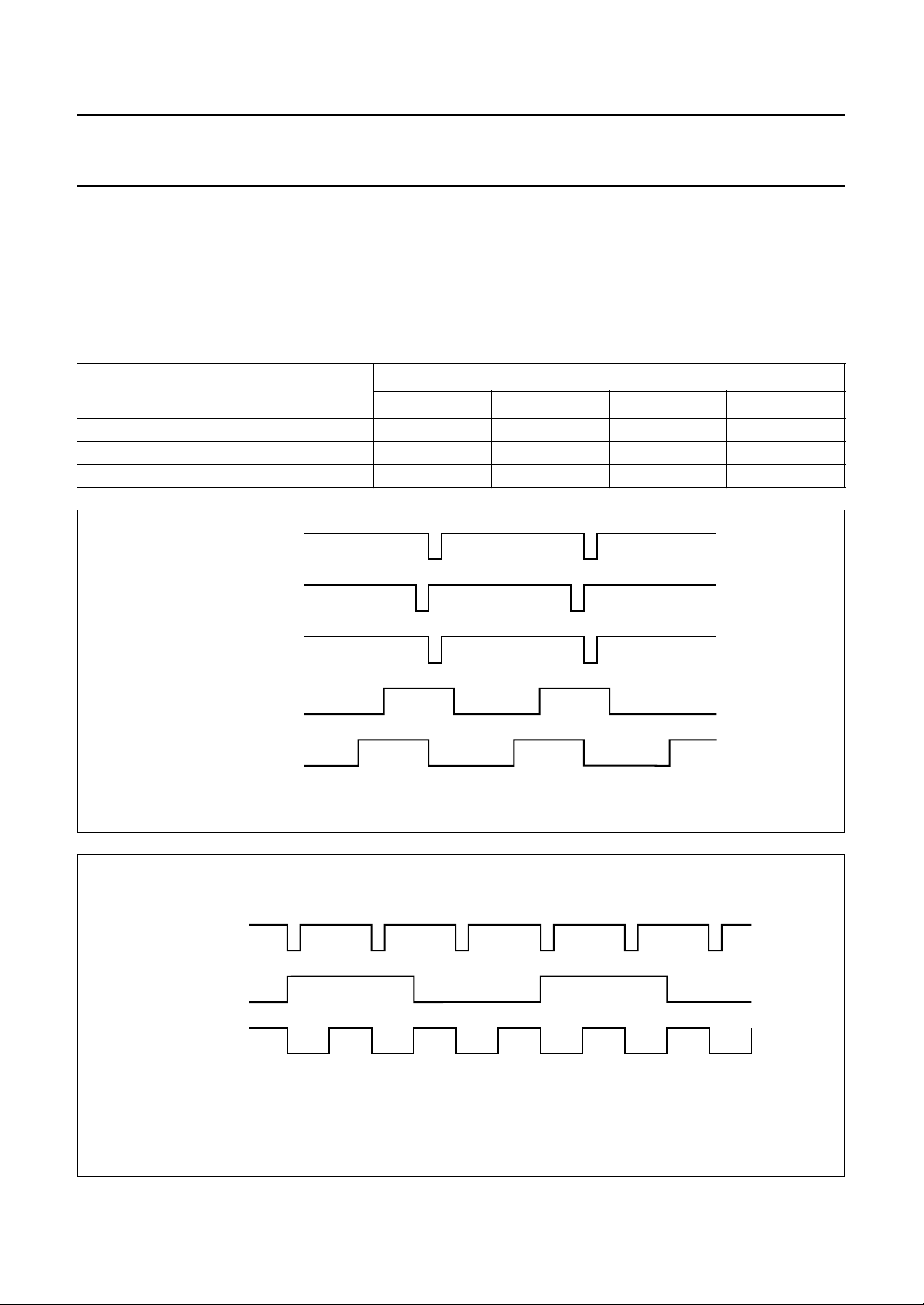
Philips Semiconductors Preliminary specification
High performance Compact
SAA7390
Disc-Recordable (CD-R) controller
15.6.1 RELATIONSHIP BETWEEN COMMUNICATION AND SYSTEM SYNCHRONIZATION
The system synchronization line (SYS_SYNC) is locked on a hardware generated frame synchronization; the decoders
sub-code, the ATIP and the encoders synchronization signals. The communication synchronization line (COM_SYNC)
has the same frequency as SYS_SYNC, except for four-times speed operation, where it is down-scaled with a factor 3.
Table 80 provides a representation between the speed and synchronization lines.
Table 79 Relationship of synchronization line frequency and speed.
SIGNAL
n=1 n=2 n=4 n=6
SYS_SYNC (full period) 13.3 6.6 3.3 2.2
SYS_SYNC (half period) 6.6 3.3 1.66 1.1
COM_SYNC (half period) 6.6 3.3 5.0 3.3
handbook, full pagewidth
decoder interrupt
SPEED (ms)
handbook, full pagewidth
decoder interrupt
ATIP sync interrupt
encoder interrupt
COM_SYNC
SYS_SYNC
MGE526
Fig.24 Phase relationship of COM_SYNC and SYS_SYNC (n = 1, n = 2).
COM_SYNC
SYS_SYNC
MGE527
Fig.25 Phase relationship of COM_SYNC and SYS_SYNC (n = 4).
1996 Jul 02 59
Page 60

Philips Semiconductors Preliminary specification
High performance Compact
SAA7390
Disc-Recordable (CD-R) controller
15.7 Microprocessor interface
V
= 4.75 to 5.25 V; VSS=0V; T
DD
SYMBOL PARAMETER MIN. MAX. UNIT
Microprocessor timing; see Figs 26, 27 and 28
t
LHLL
t
AVLL
t
LLAX
t
LLPL
t
PLPH
t
PLIV
t
PXIX
t
PXIZ
t
AVIV
t
PLAZ
t
RLRH
t
WLWH
t
RLDV
t
RHDX
t
RHDZ
t
LLDV
t
AVDV
t
LLWL
t
AVWL
t
QVWX
t
WHQX
t
RLAZ
t
WHLH
ALE pulse width 60 − ns
address valid to ALE LOW 15 − ns
address hold after ALE LOW 35 − ns
ALE LOW to PSEN LOW 25 − ns
PSEN pulse width 80 − ns
PSEN LOW to valid input instruction − 65 ns
Input instruction hold after PSEN 0 − ns
Input instruction float after PSEN − 30 ns
address to valid input instruction − 130 ns
PSEN low to address float − 6ns
UC_RD pulse width 180 − ns
UC_WR pulse width 180 − ns
UC_RD LOW to valid input data − 135 ns
data hold after UC_RD 0 − ns
data float after UC_RD − 70 ns
ALE LOW to valid input data − 235 ns
address to valid input data − 260 ns
ALE LOW to UC_RD or UC_WR LOW 90 115 ns
address LOW to UC_RD or UC_WR LOW 115 − ns
data valid to UC_WR transition 20 − ns
data hold after UC_WR 20 − ns
UC_RD LOW to address float − 0ns
UC_RD or UC_WR LOW to ALE HIGH 20 40 ns
= −10 to +70 °C; unless otherwise specified.
amb
1996 Jul 02 60
Page 61
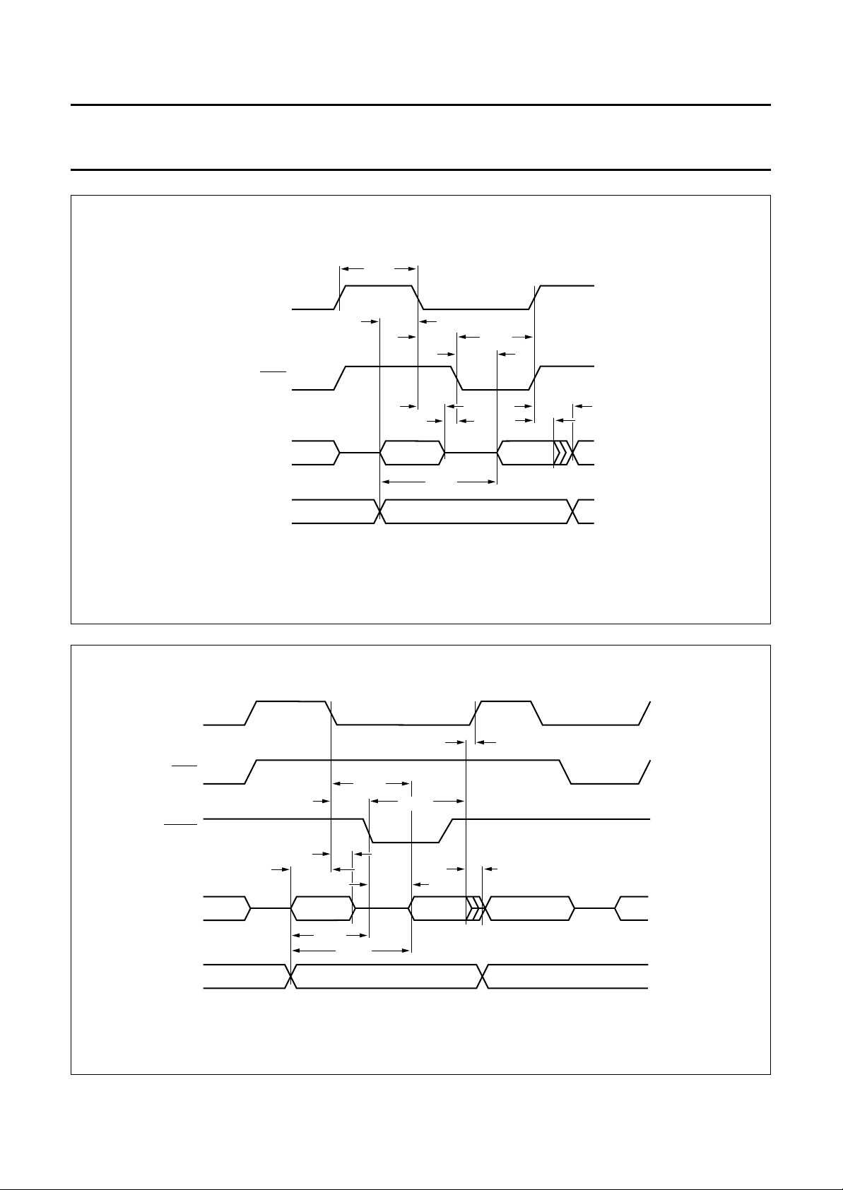
Philips Semiconductors Preliminary specification
High performance Compact
Disc-Recordable (CD-R) controller
handbook, full pagewidth
ALE
PSEN
LA7 to LA0
A15 to A8
t
LHLL
t
AVLL
t
LLPL
t
LLAX
t
AVIV
t
PLAZ
t
PLIV
t
PLPH
t
PXIX
t
PXIZ
SAA7390
MGE528
handbook, full pagewidth
UC_AD7
UC_AD0
ALE
PSEN
UC_RD
to
UC_A15
to
UC_A8
Fig.26 External program memory read cycle.
t
WHLH
t
LLDV
t
AVLL
t
AVWL
t
LLWL
t
LLAX
t
AVDV
t
RLVD
t
RLRH
t
RHDZ
MGE529
Fig.27 External data memory read cycle.
1996 Jul 02 61
Page 62
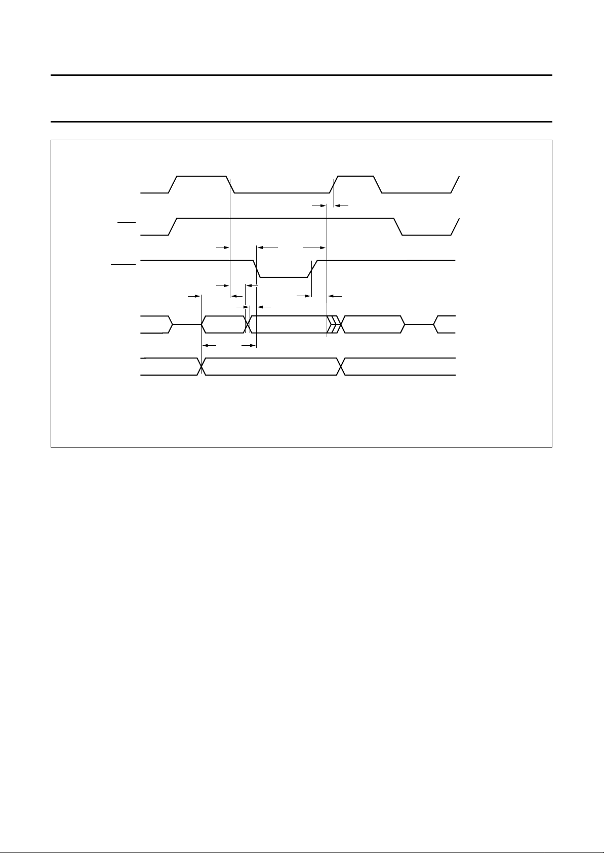
Philips Semiconductors Preliminary specification
High performance Compact
Disc-Recordable (CD-R) controller
handbook, full pagewidth
ALE
PSEN
UC_WR
UC_AD7
to
UC_AD0
UC_A15
to
UC_A8
t
AVLL
t
AVWL
t
LLWL
t
LLAX
t
RLRH
t
QVWX
t
WHLH
t
WHQX
SAA7390
MGE530
Fig.28 External data memory write cycle.
1996 Jul 02 62
Page 63
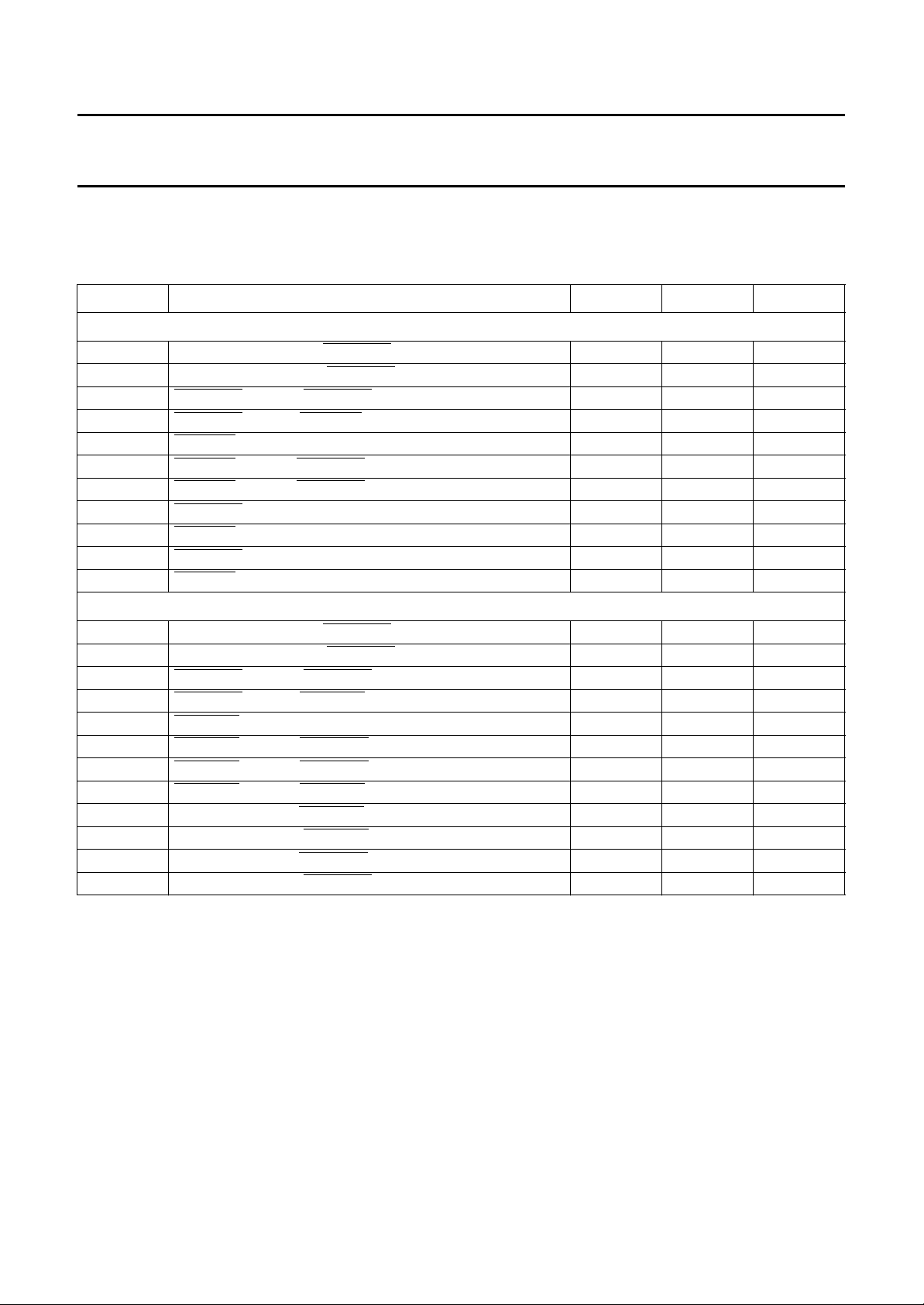
Philips Semiconductors Preliminary specification
High performance Compact
SAA7390
Disc-Recordable (CD-R) controller
15.8 Host interface
15.8.1 R
VDD= 4.75 to 5.25 V; VSS=0V; T
SYMBOL PARAMETER MIN. MAX. UNIT
Read cycle timing; see Fig.29; note 1
t
1
t
2
t
3
t
4
t
5
t
6
t
7
t
8
t
9
t
10
t
11
Write cycle timing; see Fig.30; note 1
t
1
t
2
t
3
t
4
t
5
t
6
t
7
t
8
t
9
t
10
t
11
t
12
EGISTER INTERFACE
= −10 to +70 °C; unless otherwise specified.
amb
address set-up time to HOSTSEL LOW 0 − ns
address hold time from HOSTSEL LOW 50 − ns
HOSTSEL HIGH to HOSTSEL LOW 40 − ns
HOSTSEL LOW to HOSTRD LOW 0 − ns
HOSTRD pulse width 25 − ns
HOSTRD HIGH to HOSTSEL HIGH 0 − ns
HOSTRD HIGH to HOSTSEL LOW 40 − ns
HOSTSEL LOW to data valid 0 40 ns
HOSTRD LOW to data valid 0 25 ns
HOSTSEL HIGH to data release 2 25 ns
HOSTRD HIGH to data release 2 25 ns
address set-up time to HOSTSEL LOW 0 − ns
address hold time from HOSTSEL LOW 50 − ns
HOSTSEL HIGH to HOSTSEL LOW 40 − ns
HOSTSEL LOW to HOSTWR LOW 0 − ns
HOSTWR pulse width 25 − ns
HOSTWR HIGH to HOSTSEL HIGH 0 − ns
HOSTWR HIGH to HOSTSEL LOW 40 − ns
HOSTWR HIGH to HOSTWR LOW 40 40 ns
data set-up time to HOSTWR HIGH 8 25 ns
data hold time from HOSTWR HIGH 0 25 ns
data set-up time to HOSTSEL HIGH 10 25 ns
data hold time from HOSTSEL HIGH 35 25 ns
Note
1. These timings are taken form the 53CF90; the 53CD92A/B timings are slightly different.
1996 Jul 02 63
Page 64
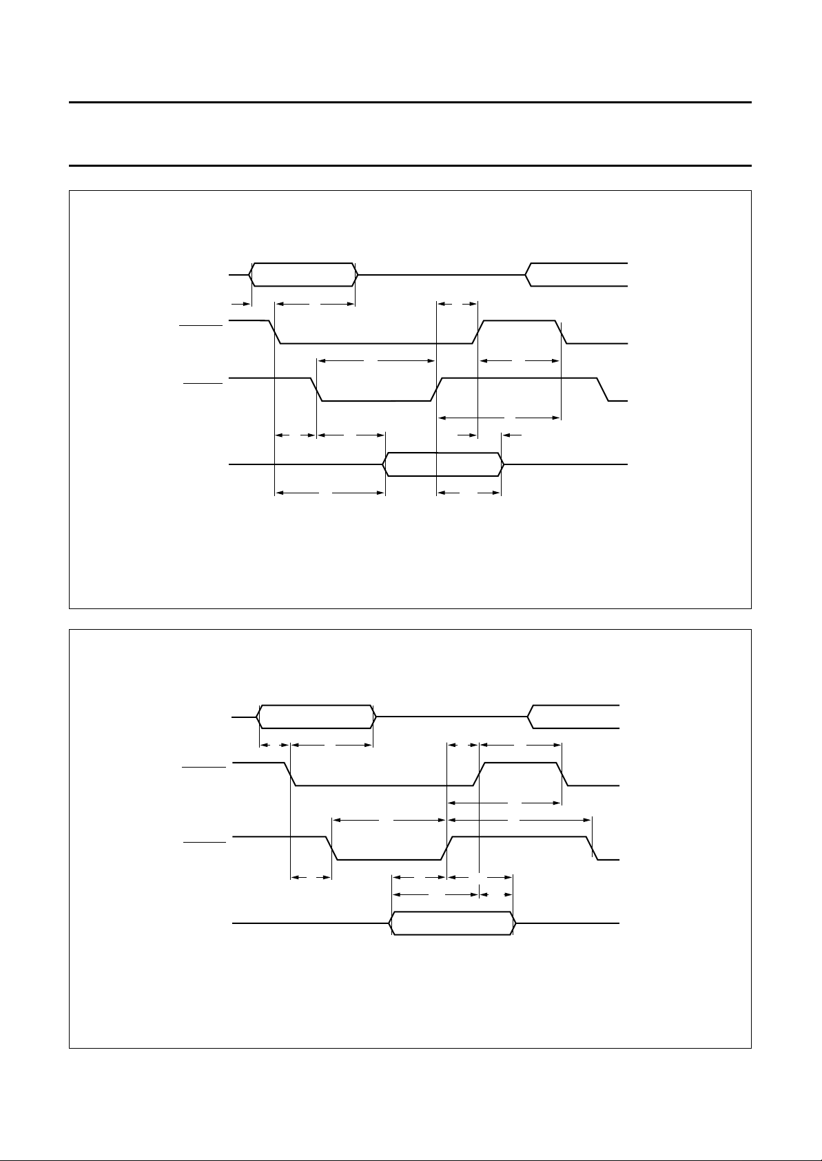
Philips Semiconductors Preliminary specification
High performance Compact
Disc-Recordable (CD-R) controller
handbook, full pagewidth
UC_AD3
to
UC_AD0
HOSTSEL
HOSTRD
UC_AD7
to
UC_AD0
t
1
t
2
t
4
t
9
t
8
SAA7390
t
6
t
5
t
11
t
3
t
7
t
10
MGE531
handbook, full pagewidth
UC_AD3
to
UC_AD0
HOSTSEL
HOSTWR
UC_AD7
to
UC_AD0
Fig.29 Register read cycle timing.
t
1
t
2
t
5
t
4
t
t
6
t
9
t
10
11
t
3
t
7
t
8
t
12
MGE532
Fig.30 Register write cycle timing.
1996 Jul 02 64
Page 65
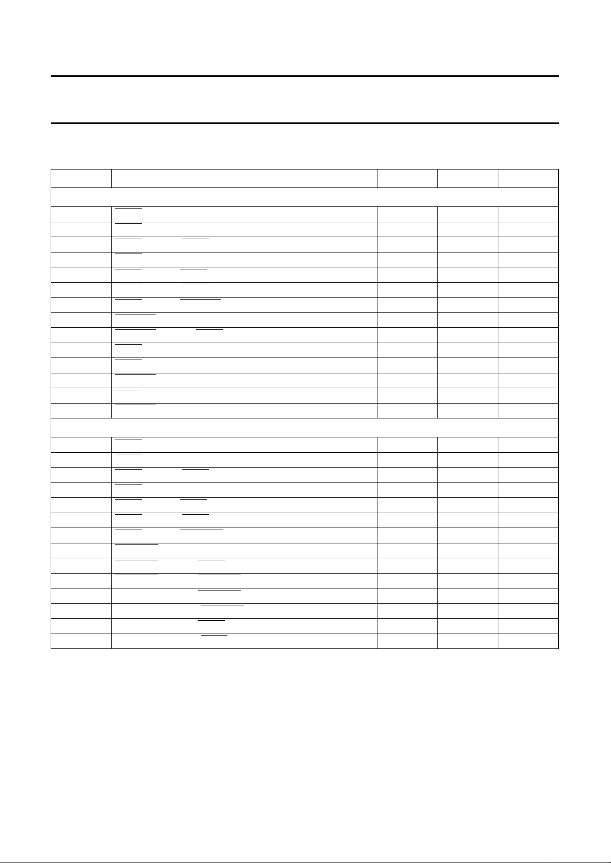
Philips Semiconductors Preliminary specification
High performance Compact
SAA7390
Disc-Recordable (CD-R) controller
15.8.2 DMA INTERFACE TIMING
VDD= 4.75 to 5.25 V; VSS=0V; T
SYMBOL PARAMETER MIN. MAX. UNIT
DMA read cycle timing; see Fig.31
t
1
t
2
t
3
t
4
t
5
t
6
t
7
t
8
t
9
t
10
t
11
t
12
t
13
t
14
DACK LOW to DREQ LOW − 20 ns
DACK HIGH to DREQ HIGH − 20 ns
DACK HIGH to DACK LOW 12 − ns
DACK pulse width 35 − ns
DACK LOW to DACK LOW 75 − ns
DACK HIGH to DACK HIGH note 1 − ns
DACK LOW to HOSTRD LOW 0 − ns
HOSTRD pulse width t
HOSTRD HIGH to DACK HIGH 0 − ns
DACK HIGH to data valid − 30 ns
DACK LOW to data valid − 25 ns
HOSTRD LOW to data valid − 25 ns
DACK HIGH to data release 2 25 ns
HOSTRD HIGH to data release 2 25 ns
DMA write cycle timing; see Fig.32
t
1
t
2
t
3
t
4
t
5
t
6
t
7
t
8
t
9
t
10
t
11
t
12
t
13
t
14
DACK LOW to DREQ LOW − 20 ns
DACK HIGH to DREQ HIGH − 20 ns
DACK HIGH to DACK LOW 12 − ns
DACK pulse width 35 − ns
DACK LOW to DACK LOW 75 − ns
DACK HIGH to DACK HIGH note 1 − ns
DACK LOW to HOSTWR LOW 0 − ns
HOSTWR pulse width 30 − ns
HOSTWR HIGH to DACK HIGH 0 − ns
HOSTWR HIGH to HOSTWR HIGH 30 − ns
data set-up time to HOSTWR HIGH 8 − ns
data hold time from HOSTWR HIGH 0 − ns
data set-up time to DACK HIGH 10 − ns
data hold time from DACK HIGH 10 − ns
= −10 to +70 °C; unless otherwise specified.
amb
12
− ns
Note
1. t
+30−t3and tCP; where tCS is the synchronization latency and tCP is the clock period.
CS
1996 Jul 02 65
Page 66
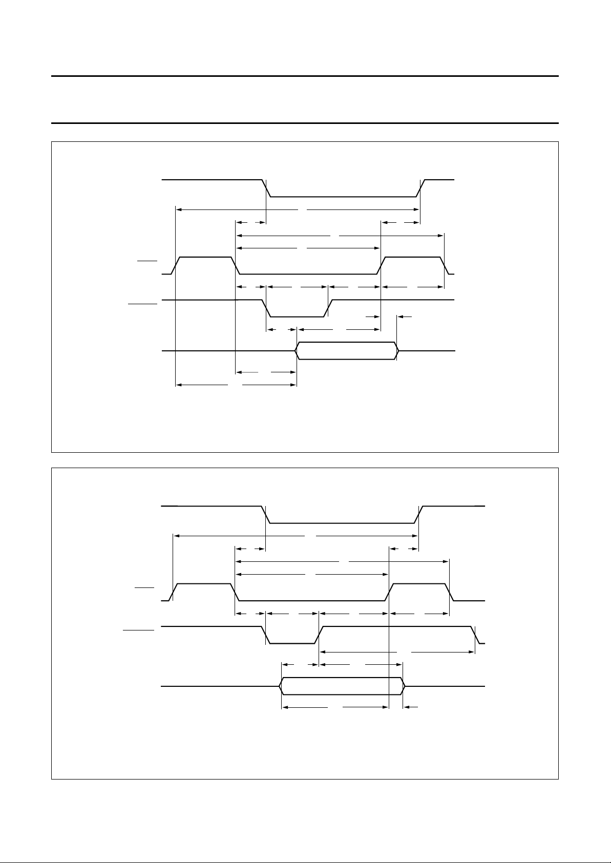
Philips Semiconductors Preliminary specification
High performance Compact
Disc-Recordable (CD-R) controller
book, full pagewidth
DREQ
DACK
HOSTRD
SD7 to SD0
t
1
t
7
t
10
SAA7390
t
6
t
t
4
t
8
t
12
t
11
5
t
9
t
14
t
2
t
3
t
13
MGE533
handbook, full pagewidth
DREQ
DACK
HOSTWR
SD7 to SD0
Fig.31 DMA read cycle timing.
t
6
t
1
t
t
4
t
7
t
8
t
11
5
t
9
t
12
t
13
t
2
t
3
t
10
t
14
MGE534
Fig.32 DMA write cycle timing.
1996 Jul 02 66
Page 67
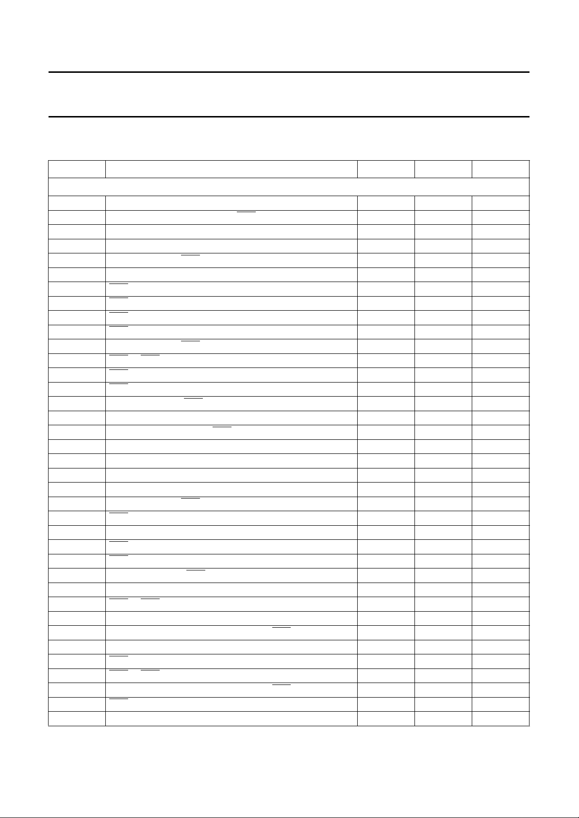
Philips Semiconductors Preliminary specification
High performance Compact
SAA7390
Disc-Recordable (CD-R) controller
15.9 DRAM interface (the SAA7390 is designed to operate with standard 70 ns DRAMs)
V
= 4.75 to 5.25 V; VSS=0V; T
DD
SYMBOL PARAMETER MIN. MAX. UNIT
DRAM interface timing; see Figs 33 to 37
t
acc;CA
t
hCA;RAS
t
su;CA
t
su;RA
t
acc;CAS
t
h;CA
t
W;CAS
t
h;CAS
t
CASLZ
t
pCAS
t
acc;pCAS
t
pCAS;RAS
t
h;CAS
t
su;CAS
t
wCASL
t
h;DAT
t
hDAT;RAS
t
su;DAT
t
d;OFF
t
cy;FPR/W
t
cy;FPR-W
t
acc;RAS
t
dRAS;CA
t
h;RA
t
W;RAS
t
W;RASFP
t
CA;RASL
t
cy;R/W
t
dRAS;CAS
t
su;R
t
hrR;CAS
t
REF
t
pRAS
t
pRAS;CAS
t
hr;RAS
t
h;RAS
t
cy;R-W
access time from column address − 35 ns
column address hold time from RAS 55 − ns
column address set-up time 0 − ns
row address set-up time 0 − ns
access time from CAS − 20 ns
column address hold time 15 − ns
CAS pulse width 20 10000 ns
CAS hold time (CBR refresh) 15 − ns
CAS to output in low impedance 3 − ns
CAS precharge time 10 − ns
access time from CAS precharge − 40 ns
CAS to RAS precharge time 5 − ns
CAS hold time 70 − ns
CAS set-up time (CBR refresh) 5 − ns
write command to CAS lead time 20 − ns
data input hold time 15 − ns
data input hold time from RAS 55 − ns
data input set-up time 0 − ns
output buffer turn off delay 3 20 ns
fast page mode read or write cycle time 40 − ns
fast page mode read-write cycle time n/a
access time from RAS − 70 ns
RAS to column address delay time 15 35 ns
row address hold time 10 − ns
RAS pulse width 70 10000 ns
RAS pulse width (fast page mode) 70 100000 ns
column address to RAS lead time 35 − ns
random read or write cycle time 130 − ns
RAS to CAS delay time 20 50 ns
read command set-up time 0 − ns
read command hold time (referenced to CAS) 0 − ns
refresh period − 32 ns
RAS precharge time 50 − ns
RAS to CAS precharge time 0 − ns
read command hold time (referenced to RAS) 0 − ns
RAS hold time 20 − ns
read-write cycle time n/a
= −10 to +70 °C; unless otherwise specified.
amb
(1)
(1)
− ns
− ns
1996 Jul 02 67
Page 68
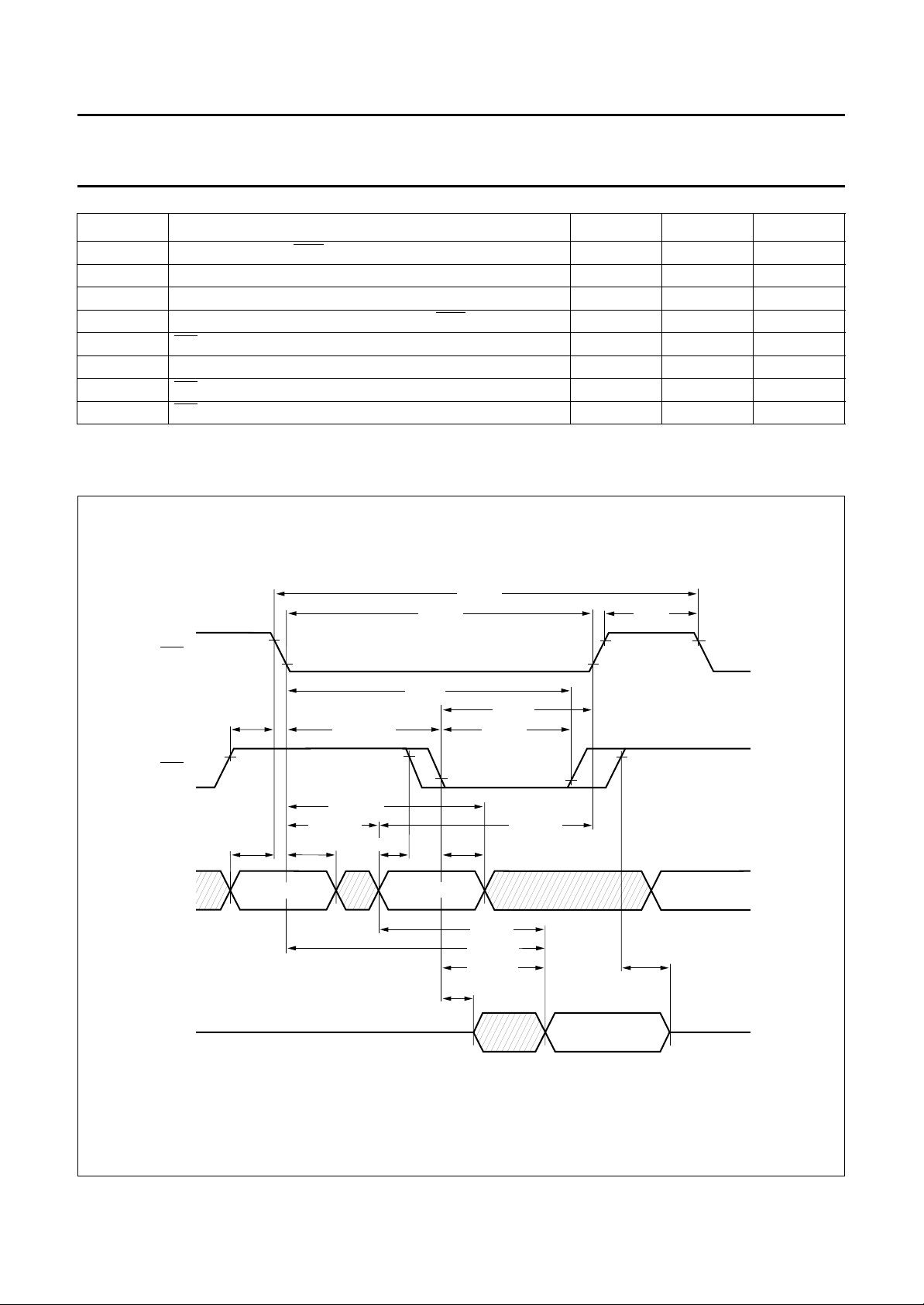
Philips Semiconductors Preliminary specification
High performance Compact
SAA7390
Disc-Recordable (CD-R) controller
SYMBOL PARAMETER MIN. MAX. UNIT
t
RASL;W
t
trans
t
hW
t
hW;RAS
t
su;WE
t
W;W
t
h;WE
t
su;WE
Note
1. Not applicable.
write command to RAS lead time 20 − ns
transition time (rise or fall) 3 50 ns
write command hold time 15 − ns
write command hold time (referenced to RAS) 55 − ns
WE command set-up time 0 − ns
write command pulse width 15 − ns
WE hold time (CBR refresh) 10 − ns
WE set-up time (CBR refresh) 10 − ns
andbook, full pagewidth
RAS
CAS
ADDRESS
DATA
t
pCAS;RAS
t
su;RA
ROW
t
dRAS;CA
t
h;RA
t
dRAS;CAS
t
hCA;RAS
t
su;CA
t
W;RAS
t
h;CAS
COLUMN
t
cy;R/W
t
h;CA
t
CASLZ
t
t
W;CAS
t
acc;CA
t
acc;RAS
t
acc;CAS
h;RAS
t
CA;RASL
t
pRAS
t
d;OFF
ROW
MGE412
Fig.33 DRAM read cycle.
1996 Jul 02 68
Page 69
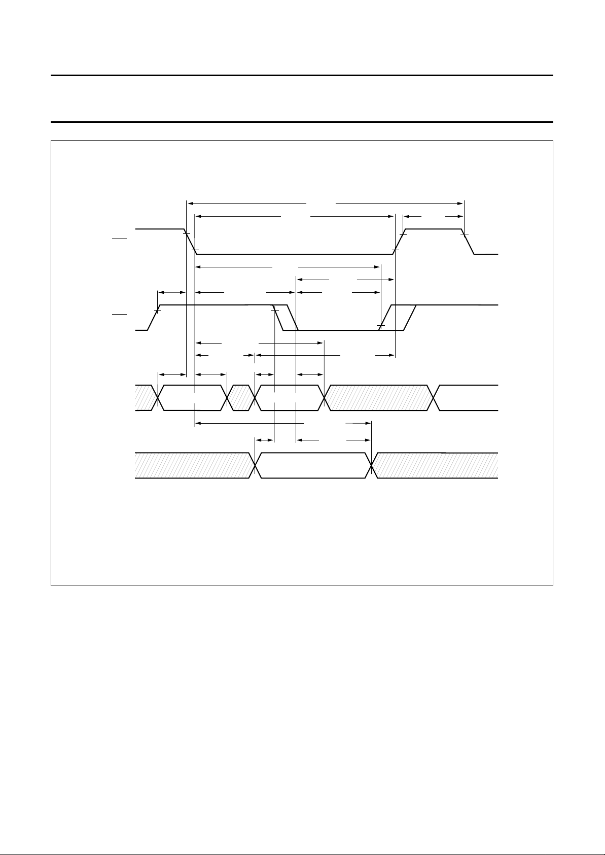
Philips Semiconductors Preliminary specification
High performance Compact
Disc-Recordable (CD-R) controller
handbook, full pagewidth
RAS
t
CAS
pCAS;RAS
t
su;RA
t
dRAS;CA
t
h;RA
t
dRAS;CAS
t
hCA;RAS
t
su;CA
t
W;RAS
t
h;CAS
t
h;CA
t
cy;R/W
t
h;RAS
t
W;CAS
t
CA;RASL
t
pRAS
SAA7390
ADDRESS
DATA
ROW
COLUMN
t
t
su;DAT
hDAT;RAS
t
h;DAT
Fig.34 DRAM early write cycle.
ROW
MGE413
1996 Jul 02 69
Page 70
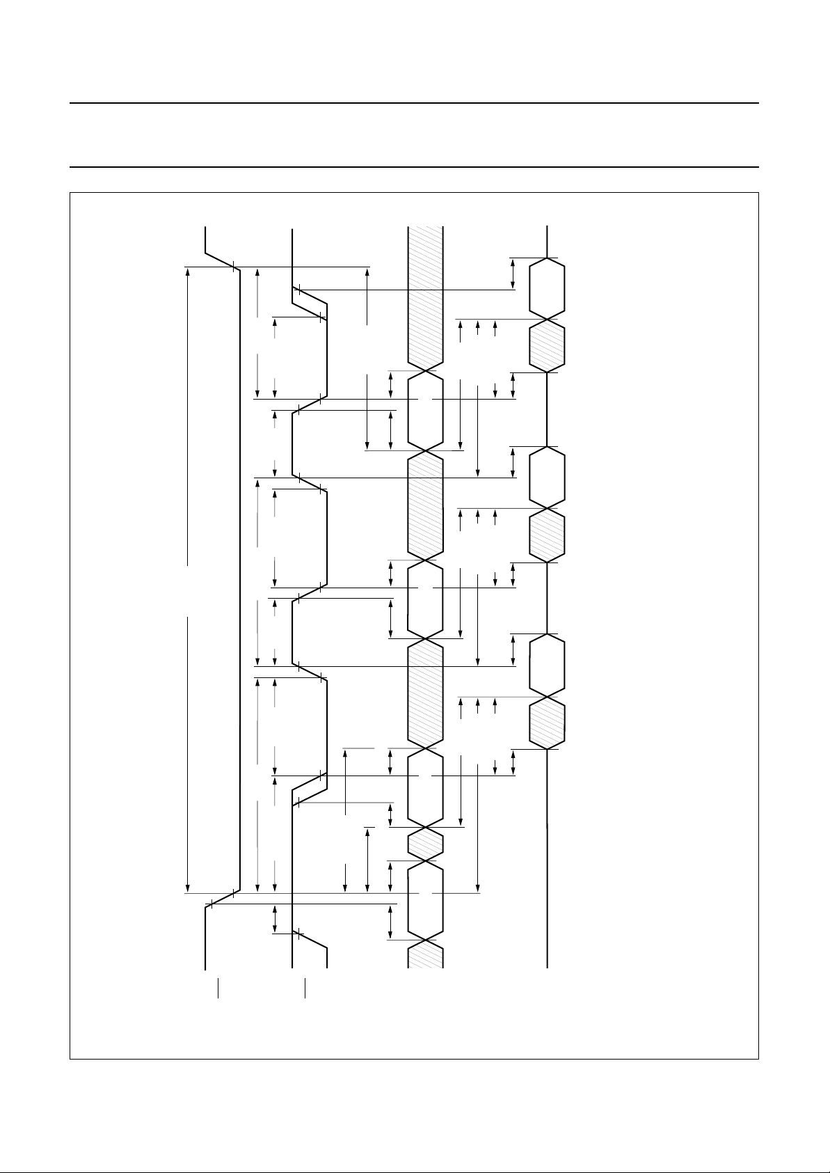
Philips Semiconductors Preliminary specification
High performance Compact
Disc-Recordable (CD-R) controller
h;RAS
t
CA;RASL
W;CAS
t
pCAS
t
t
h;CA
t
su;CA
t
t
COLUMN
acc;CA
acc;pCAS
t
d;OFF
t
acc;CAS
t
d;OFF
t
CASLZ
t
SAA7390
MGE414
ndbook, full pagewidth
W;RASFP
t
W;CAS
t
cy;FPR/W
t
pCAS
t
W;CAS
t
h;CAS
t
dRAS;CAS
t
pCAS;RAS
t
hCA;RAS
t
dRAS;CA
t
h;CA
t
su;CA
t
h;CA
t
su;CA
t
h;RA
t
su;RA
t
t
t
COLUMN COLUMN
ROW
acc;CA
acc;pCAS
t
acc;CA
acc;pCAS
t
acc;CAS
t
d;OFF
t
acc;CAS
t
CASLZ
t
CASLZ
t
Fig.35 Fast page mode DRAM read cycle.
RAS
CAS
1996 Jul 02 70
DATA
ADDRESS
Page 71
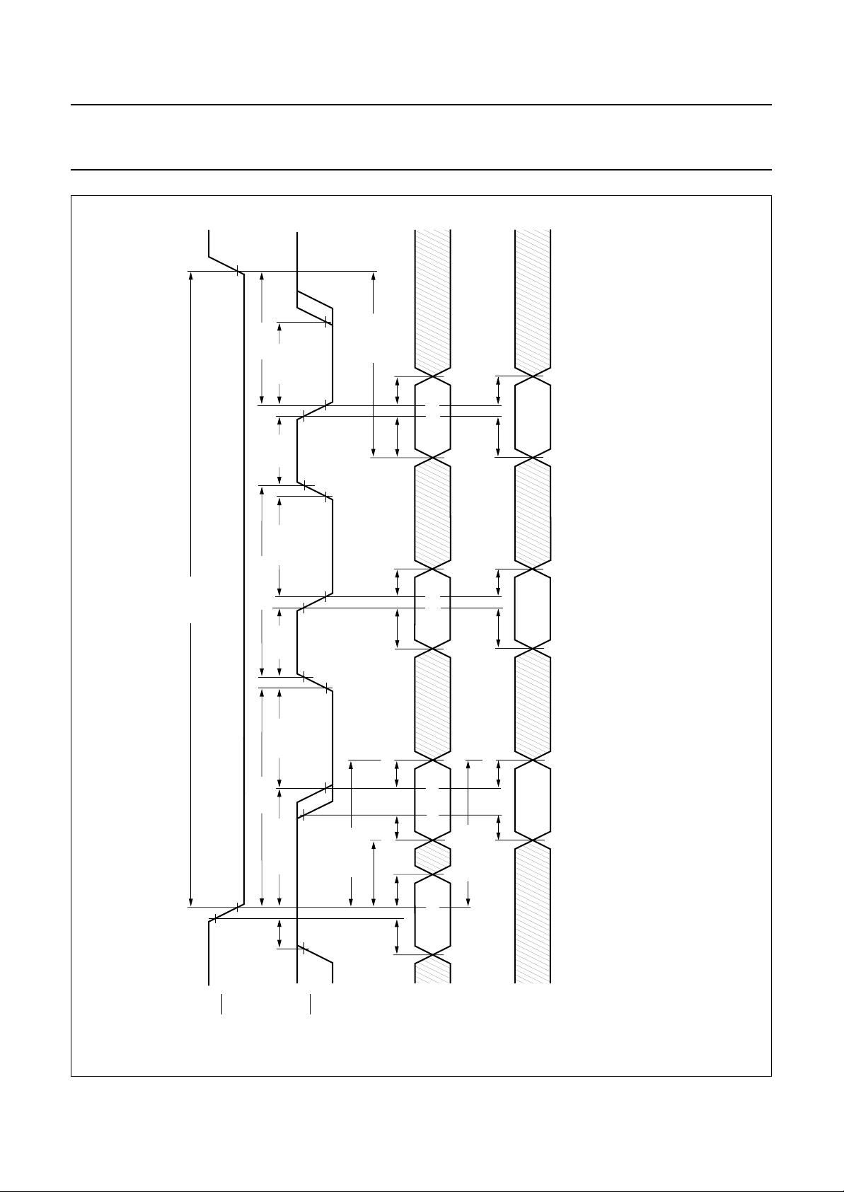
Philips Semiconductors Preliminary specification
High performance Compact
Disc-Recordable (CD-R) controller
h;RAS
t
W;CAS
t
pCAS
t
CA;RASL
t
h;CA
t
su;CA
t
COLUMN
h;DAT
t
su;DAT
t
SAA7390
MGE415
ndbook, full pagewidth
W;RAS
t
W;CAS
t
cy;FPR/W
t
pCAS
t
W;CAS
t
h;CAS
t
dRAS;CAS
t
pCAS;RAS
t
hCA;RAS
t
dRAS;CA
t
h;CA
t
su;CA
t
h;CA
t
su;CA
t
h;RA
t
su;RA
t
COLUMN COLUMN
t
ROW
h;DAT
t
su;DAT
t
h;DAT
t
su;DAT
t
hDAT;RAS
Fig.36 Fast page mode DRAM write cycle.
RAS
CAS
1996 Jul 02 71
DATA
ADDRESS
Page 72
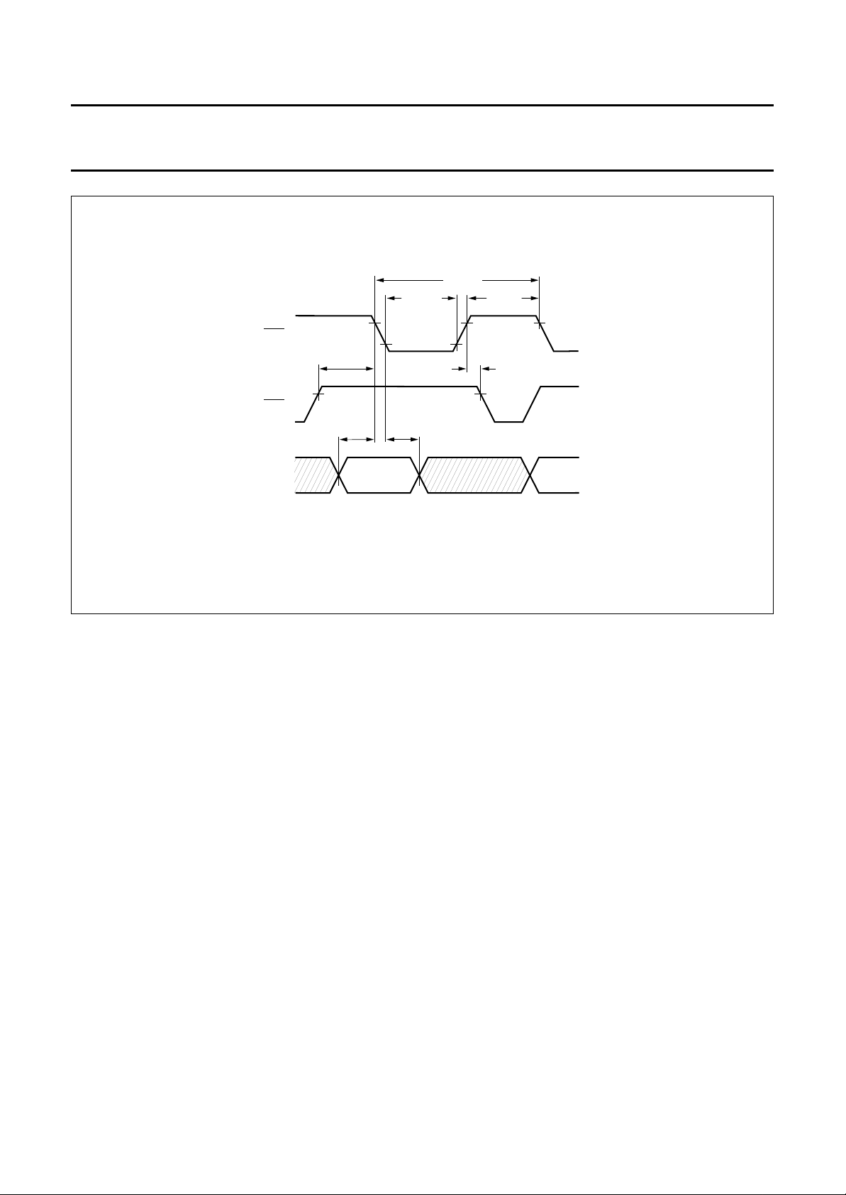
Philips Semiconductors Preliminary specification
High performance Compact
Disc-Recordable (CD-R) controller
handbook, full pagewidth
RAS
t
pCAS;RAS
CAS
t
su;RA
ADDRESS
t
cy;R/W
t
W;RAS
t
h;RA
ROW ROW
t
pRAS
t
pRAS;CAS
MGE416
SAA7390
Fig.37 DRAM refresh cycle.
1996 Jul 02 72
Page 73
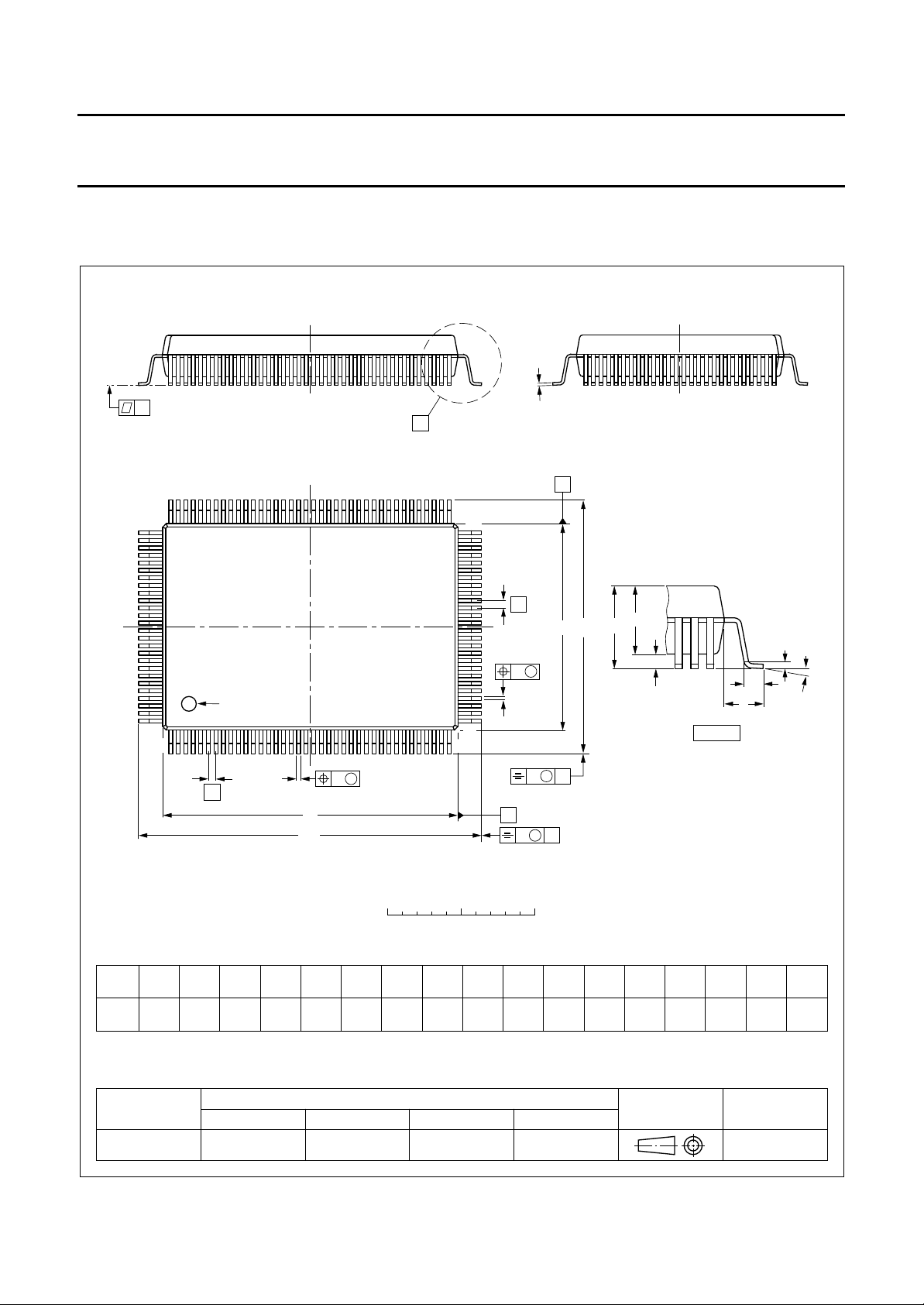
Philips Semiconductors Preliminary specification
High performance Compact
SAA7390
Disc-Recordable (CD-R) controller
16 PACKAGE OUTLINE
SQFP128: plastic shrink quad flat package; 128 leads (lead length 1.6 mm); body 14 x 20 x 2.8 mm
c
y
X
A
102 65
103
64
SOT387-2
pin 1 index
128
1
w M
b
e
DIMENSIONS (mm are the original dimensions)
A
A
UNIT
max. min.
mm
3.40
Note
1. Plastic or metal protrusions of 0.25 mm maximum per side are not included.
1
A
2
3.05
2.55
p
D
H
D
0 5 10 mm
A
b
3
p
0.27
0.17
0.20
0.09
0.250.25
(1)
cE
D
38
scale
(1)
14.020.0 0.50
e
H
E
E
w M
b
p
39
v M
A
B
v M
B
eH
H
23.2
D
E
17.2
A
2
A
A
1
LL
p
0.95
0.65
detail X
0.08 0.100.201.60
(A )
L
p
L
ywv θ
3
θ
o
7
o
0
OUTLINE
VERSION
SOT387-2
IEC JEDEC EIAJ
REFERENCES
1996 Jul 02 73
EUROPEAN
PROJECTION
ISSUE DATE
96-03-14
Page 74

Philips Semiconductors Preliminary specification
High performance Compact
Disc-Recordable (CD-R) controller
17 SOLDERING
17.1 Introduction
There is no soldering method that is ideal for all IC
packages. Wave soldering is often preferred when
through-hole and surface mounted components are mixed
on one printed-circuit board. However, wave soldering is
not always suitable for surface mounted ICs, or for
printed-circuits with high population densities. In these
situations reflow soldering is often used.
This text gives a very brief insight to a complex technology.
A more in-depth account of soldering ICs can be found in
our
“IC Package Databook”
17.2 Reflow soldering
Reflow soldering techniques are suitable for all QFP
packages.
The choice of heating method may be influenced by larger
plastic QFP packages (44 leads, or more). If infrared or
vapour phase heating is used and the large packages are
not absolutely dry (less than 0.1% moisture content by
weight), vaporization of the small amount of moisture in
them can cause cracking of the plastic body. For more
information, refer to the Drypack chapter in our
Reference Handbook”
Reflow soldering requires solder paste (a suspension of
fine solder particles, flux and binding agent) to be applied
to the printed-circuit board by screen printing, stencilling or
pressure-syringe dispensing before package placement.
Several techniques exist for reflowing; for example,
thermal conduction by heated belt. Dwell times vary
between 50 and 300 seconds depending on heating
method. Typical reflow temperatures range from
215 to 250 °C.
Preheating is necessary to dry the paste and evaporate
the binding agent. Preheating duration: 45 minutes at
45 °C.
(order code 9398 652 90011).
“Quality
(order code 9397 750 00192).
SAA7390
17.3 Wave soldering
Wave soldering is not recommended for QFP packages.
This is because of the likelihood of solder bridging due to
closely-spaced leads and the possibility of incomplete
solder penetration in multi-lead devices.
If wave soldering cannot be avoided, the following
conditions must be observed:
• A double-wave (a turbulent wave with high upward
pressure followed by a smooth laminar wave)
soldering technique should be used.
• The footprint must be at an angle of 45° to the board
direction and must incorporate solder thieves
downstream and at the side corners.
Even with these conditions, do not consider wave
soldering the following packages: QFP52 (SOT379-1),
QFP100 (SOT317-1), QFP100 (SOT317-2),
QFP100 (SOT382-1) or QFP160 (SOT322-1).
During placement and before soldering, the package must
be fixed with a droplet of adhesive. The adhesive can be
applied by screen printing, pin transfer or syringe
dispensing. The package can be soldered after the
adhesive is cured.
Maximum permissible solder temperature is 260 °C, and
maximum duration of package immersion in solder is
10 seconds, if cooled to less than 150 °C within
6 seconds. Typical dwell time is 4 seconds at 250 °C.
A mildly-activated flux will eliminate the need for removal
of corrosive residues in most applications.
17.4 Repairing soldered joints
Fix the component by first soldering two diagonallyopposite end leads. Use only a low voltage soldering iron
(less than 24 V) applied to the flat part of the lead. Contact
time must be limited to 10 seconds at up to 300 °C. When
using a dedicated tool, all other leads can be soldered in
one operation within 2 to 5 seconds between
270 and 320 °C.
1996 Jul 02 74
Page 75

Philips Semiconductors Preliminary specification
High performance Compact
SAA7390
Disc-Recordable (CD-R) controller
18 DEFINITIONS
Data sheet status
Objective specification This data sheet contains target or goal specifications for product development.
Preliminary specification This data sheet contains preliminary data; supplementary data may be published later.
Product specification This data sheet contains final product specifications.
Limiting values
Limiting values given are in accordance with the Absolute Maximum Rating System (IEC 134). Stress above one or
more of the limiting values may cause permanent damage to the device. These are stress ratings only and operation
of the device at these or at any other conditions above those given in the Characteristics sections of the specification
is not implied. Exposure to limiting values for extended periods may affect device reliability.
Application information
Where application information is given, it is advisory and does not form part of the specification.
19 LIFE SUPPORT APPLICATIONS
These products are not designed for use in life support appliances, devices, or systems where malfunction of these
products can reasonably be expected to result in personal injury. Philips customers using or selling these products for
use in such applications do so at their own risk and agree to fully indemnify Philips for any damages resulting from such
improper use or sale.
1996 Jul 02 75
Page 76

Philips Semiconductors – a worldwide company
Argentina: see South America
Australia: 34 Waterloo Road, NORTH RYDE, NSW 2113,
Tel. +61 2 9805 4455, Fax. +61 2 9805 4466
Austria: Computerstr. 6, A-1101 WIEN, P.O. Box 213,
Tel. +43 1 60 101, Fax. +43 1 60 101 1210
Belarus: Hotel Minsk Business Center, Bld. 3, r. 1211, Volodarski Str. 6,
220050 MINSK, Tel. +375 172 200 733, Fax. +375 172 200 773
Belgium: see The Netherlands
Brazil: see South America
Bulgaria: Philips Bulgaria Ltd., Energoproject, 15th floor,
51 James Bourchier Blvd., 1407 SOFIA,
Tel. +359 2 689 211, Fax. +359 2 689 102
Canada: PHILIPS SEMICONDUCTORS/COMPONENTS,
Tel. +1 800 234 7381, Fax. +1 708 296 8556
China/Hong Kong: 501 Hong Kong Industrial Technology Centre,
72 Tat Chee Avenue, Kowloon Tong, HONG KONG,
Tel. +852 2319 7888, Fax. +852 2319 7700
Colombia: see South America
Czech Republic: see Austria
Denmark: Prags Boulevard 80, PB 1919, DK-2300 COPENHAGEN S,
Tel. +45 32 88 2636, Fax. +45 31 57 1949
Finland: Sinikalliontie 3, FIN-02630 ESPOO,
Tel. +358 615 800, Fax. +358 615 80920
France: 4 Rue du Port-aux-Vins, BP317, 92156 SURESNES Cedex,
Tel. +33 1 40 99 6161, Fax. +33 1 40 99 6427
Germany: Hammerbrookstraße 69, D-20097 HAMBURG,
Tel. +49 40 23 52 60, Fax. +49 40 23 536 300
Greece: No. 15, 25th March Street, GR 17778 TAVROS,
Tel. +30 1 4894 339/911, Fax. +30 1 4814 240
Hungary: see Austria
India: Philips INDIA Ltd, Shivsagar Estate, A Block, Dr. Annie Besant Rd.
Worli, MUMBAI 400 018, Tel. +91 22 4938 541, Fax. +91 22 4938 722
Indonesia: see Singapore
Ireland: Newstead, Clonskeagh, DUBLIN 14,
Tel. +353 1 7640 000, Fax. +353 1 7640 200
Israel: RAPAC Electronics, 7 Kehilat Saloniki St, TEL AVIV 61180,
Tel. +972 3 645 0444, Fax. +972 3 648 1007
Italy: PHILIPS SEMICONDUCTORS, Piazza IV Novembre 3,
20124 MILANO, Tel. +39 2 6752 2531, Fax. +39 2 6752 2557
Japan: Philips Bldg 13-37, Kohnan 2-chome, Minato-ku, TOKYO 108,
Tel. +81 3 3740 5130, Fax. +81 3 3740 5077
Korea: Philips House, 260-199 Itaewon-dong, Yongsan-ku, SEOUL,
Tel. +82 2 709 1412, Fax. +82 2 709 1415
Malaysia: No. 76 Jalan Universiti, 46200 PETALING JAYA, SELANGOR,
Tel. +60 3 750 5214, Fax. +60 3 757 4880
Mexico: 5900 Gateway East, Suite 200, EL PASO, TEXAS 79905,
Tel. +1 800 234 7381, Fax. +1 708 296 8556
Middle East: see Italy
Netherlands: Postbus 90050, 5600 PB EINDHOVEN, Bldg. VB,
Tel. +31 40 27 83749, Fax. +31 40 27 88399
New Zealand: 2 Wagener Place, C.P.O. Box 1041, AUCKLAND,
Tel. +64 9 849 4160, Fax. +64 9 849 7811
Norway: Box 1, Manglerud 0612, OSLO,
Tel. +47 22 74 8000, Fax. +47 22 74 8341
Philippines: Philips Semiconductors Philippines Inc.,
106 Valero St. Salcedo Village, P.O. Box 2108 MCC, MAKATI,
Metro MANILA, Tel. +63 2 816 6380, Fax. +63 2 817 3474
Poland: Ul. Lukiska 10, PL 04-123 WARSZAWA,
Tel. +48 22 612 2831, Fax. +48 22 612 2327
Portugal: see Spain
Romania: see Italy
Russia: Philips Russia, Ul. Usatcheva 35A, 119048 MOSCOW,
Tel. +7 095 926 5361, Fax. +7 095 564 8323
Singapore: Lorong 1, Toa Payoh, SINGAPORE 1231,
Tel. +65 350 2538, Fax. +65 251 6500
Slovakia: see Austria
Slovenia: see Italy
South Africa: S.A. PHILIPS Pty Ltd., 195-215 Main Road Martindale,
2092 JOHANNESBURG, P.O. Box 7430 Johannesburg 2000,
Tel. +27 11 470 5911, Fax. +27 11 470 5494
South America: Rua do Rocio 220, 5th floor, Suite 51,
04552-903 São Paulo, SÃO PAULO - SP, Brazil,
Tel. +55 11 821 2333, Fax. +55 11 829 1849
Spain: Balmes 22, 08007 BARCELONA,
Tel. +34 3 301 6312, Fax. +34 3 301 4107
Sweden: Kottbygatan 7, Akalla, S-16485 STOCKHOLM,
Tel. +46 8 632 2000, Fax. +46 8 632 2745
Switzerland: Allmendstrasse 140, CH-8027 ZÜRICH,
Tel. +41 1 488 2686, Fax. +41 1 481 7730
Taiwan: PHILIPS TAIWAN Ltd., 23-30F, 66,
Chung Hsiao West Road, Sec. 1, P.O. Box 22978,
TAIPEI 100, Tel. +886 2 382 4443, Fax. +886 2 382 4444
Thailand: PHILIPS ELECTRONICS (THAILAND) Ltd.,
209/2 Sanpavuth-Bangna Road Prakanong, BANGKOK 10260,
Tel. +66 2 745 4090, Fax. +66 2 398 0793
Turkey: Talatpasa Cad. No. 5, 80640 GÜLTEPE/ISTANBUL,
Tel. +90 212 279 2770, Fax. +90 212 282 6707
Ukraine: PHILIPS UKRAINE, 2A Akademika Koroleva str., Office 165,
252148 KIEV, Tel. +380 44 476 0297/1642, Fax. +380 44 476 6991
United Kingdom: Philips Semiconductors Ltd., 276 Bath Road, Hayes,
MIDDLESEX UB3 5BX, Tel. +44 181 730 5000, Fax. +44 181 754 8421
United States: 811 East Arques Avenue, SUNNYVALE, CA 94088-3409,
Tel. +1 800 234 7381, Fax. +1 708 296 8556
Uruguay: see South America
Vietnam: see Singapore
Yugoslavia: PHILIPS, Trg N. Pasica 5/v, 11000 BEOGRAD,
Tel. +381 11 825 344, Fax.+381 11 635 777
For all other countries apply to: Philips Semiconductors, Marketing & Sales Communications,
Building BE-p, P.O. Box 218, 5600 MD EINDHOVEN, The Netherlands, Fax. +31 40 27 24825
© Philips Electronics N.V. 1996 SCA50
All rights are reserved. Reproduction in whole or in part is prohibited without the prior written consent of the copyright owner.
The information presented in this document does not form part of any quotation or contract, is believed to be accurate and reliable and may be changed
without notice. No liability will be accepted by the publisher for any consequence of its use. Publication thereof does not convey nor imply any license
under patent- or other industrial or intellectual property rights.
Printed in The Netherlands 517021/50/01/pp76 Date of release: 1996 Jul 02 Document order number: 9397 750 00942
Internet: http://www.semiconductors.philips.com/ps/
(1) SAA7390_1 June 26, 1996 11:51 am
 Loading...