

Page 1

INTEGRATED CIRCUITS
DATA SH EET
SAA7388
Error correction and host interface
IC for CD-ROM (ELM)
Preliminary specification
File under Integrated Circuits, IC01
1996 Apr 26
Page 2

Philips Semiconductors Preliminary specification
Error correction and host interface IC for
CD-ROM (ELM)
CONTENTS
1 FEATURES
2 GENERAL DESCRIPTION
3 QUICK REFERENCE DATA
4 ORDERING INFORMATION
5 BLOCK DIAGRAM
6 PINNING
7 FUNCTIONAL DESCRIPTION
7.1 CD-DSP interface and data input
7.2 Error correction and EDC check
7.3 Host interface
7.4 Subcode channel Q-to-W buffering
7.5 External buffer memory
7.6 Sub-CPU registers
7.7 Register Descriptions
7.8 Sub-CPU interface
7.9 Host registers
.10 CD-DSP Timings
8 LIMITING VALUES
9 THERMAL CHARACTERISTICS
10 CHARACTERISTICS
11 TIMING CHARACTERISTICS
11.1 Q-to-W subcode interface timing
11.2 External memory SRAM timing
11.3 External memory DRAM timing
11.4 Sub-CPU interface timing
11.5 ATAPI host interface timing
11.6 SANYO compatibility mode host interface
timing
11.7 Oak compatibility mode host interface timing
11.8 Crystal oscillator
12 PACKAGE OUTLINE
13 SOLDERING
14 DEFINITIONS
15 LIFE SUPPORT APPLICATIONS
SAA7388
1996 Apr 26 2
Page 3
Philips Semiconductors Preliminary specification
Error correction and host interface IC for
CD-ROM (ELM)
1 FEATURES
• CD-ROM (Mode 1) and CD-I (Mode 2 - Form 1 and
Form 2) formats supported
• Real-time error detection and correction in hardware
• Suitable for octal speed, n = 8.
• Maximum host transfer burst rate of 13.3 Mbyte/s
• Corrects two errors per symbol with erasure correction
• 36 kbit of on-chip error correction buffer RAM
• 12-byte command FIFO and 12-byte status FIFO
• Compatible with the Advanced Technology Attachment
(ATA) register set and the Advanced Technology
Attachment Program Interface (ATAPI) command set
• Operates with popular memories. (up to 128 kbyte
SRAM; 1 to 16 Mbit DRAM, different speed grades,
nibble or byte wide)
• Interface to Integrated Drive Electronics (IDE) bus
without external bus drivers
• Q-to-W subcode buffering, de-interleaving and
correction are supported
• Device can operate with audio RAMs. A RAM test allows
bad segments to be identified.
SAA7388
2 GENERAL DESCRIPTION
The SAA7388 decoder is a block decoder buffer manager
for high-speed CD-ROM applications that integrates
real-time error correction and detection and host interface
data transfer functions into a single chip.
The SAA7388 has an on-chip 36-kbit memory. This
memory is used as a buffer memory for error and erasure
corrections. The chip also has a buffer memory interface
thus enabling the connection of SRAM up to 128 kbytes, or
DRAM up to 16 Mbits. The on-chip memory is sufficient to
buffer 1 sector of data. The external memory can buffer
many more, depending on memory size.
The error corrector of the SAA7388 can perform 2-pass
error correction in real-time. Buffer memory for this
correction is integrated on-chip.
The SAA7388 has an host interface that is compatible with
the SANYO LC89510 or OAK OTI-012 and also
compatible with the ATA/IDE/ATAPI hard disc interface
bus. (All ATAPI registers are present in hardware).
Supply of this Compact Disc IC does not convey an implied
license under any patent right to use this IC in any
Compact Disc application.
3 QUICK REFERENCE DATA
SYMBOL PARAMETER MIN. TYP. MAX. UNIT
V
V
I
DDD
f
clk
T
T
DDD1
DDD2
amb
stg
digital supply voltage 1 3.0 3.3 3.6 V
digital supply voltage 2 4.5 5 5.5 V
supply current − 60 − mA
clock frequency 15.2 48 50.4 MHz
operating ambient temperature 0 − +70 °C
storage temperature −55 − +125 °C
4 ORDERING INFORMATION
PACKAGE
TYPE NUMBER
NAME DESCRIPTION VERSION
SAA7388GP QFP80 plastic quad flat package; 80 leads; lead length 1.95 mm;
SOT318-2
body 14 × 20 × 2.8 mm
1996 Apr 26 3
Page 4
Philips Semiconductors Preliminary specification
Error correction and host interface IC for
CD-ROM (ELM)
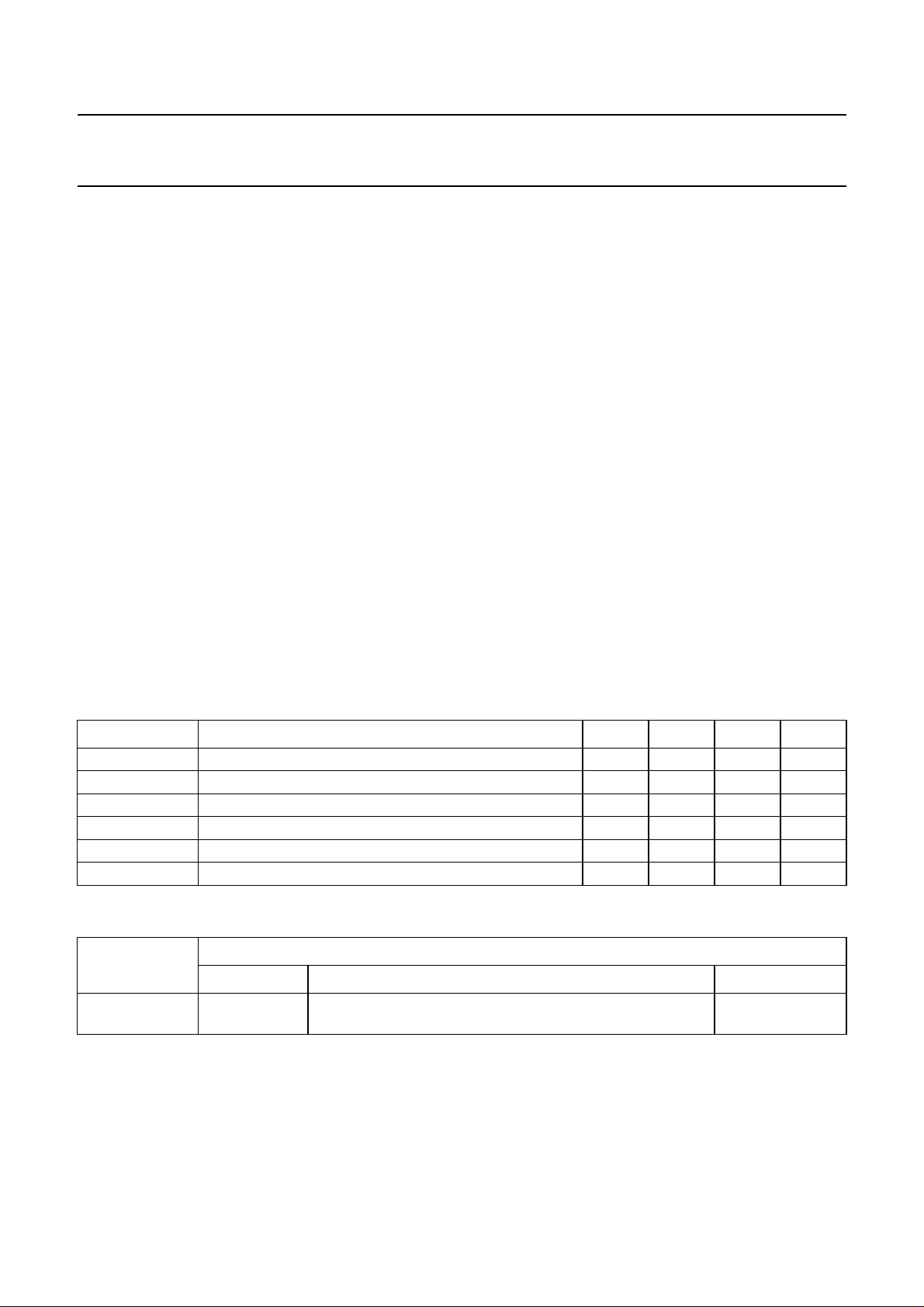
5 BLOCK DIAGRAM
handbook, full pagewidth
V
DDD1
SDA
SCL
INT
RESET
SYN
DMACK
DA1
DA2/EJECT
CS2/SELRQ
IOCS16
1, 14, 24,
41, 59, 68
32
36
37
38
39
40
45
70
71
72
73
DGND
CONTROLLER
V
MICRO-
INTERFACE
DDD2
RCK
SFSY
50, 74 28
HOST INTERFACE
BCKWSDATA
SUB
29 30 31 33 34 35 23 25
DECODER
SERIAL
INTERFACE
ERROR
CORRECTOR
SRAM
CACHE
C2PO TEST1
TEST2
TEST
SAA7388
MEMORY
MANAGER
OSCILLATOR
SAA7388
75-80
2-10
12
11
13
15-22
27
26
RA0 to RA5
RA6 to RA14
RA16/CAS
RA15/RAS
RWE
RD0 to RD7
CRIN
CROUT
42 43 44 69 46 47 48 49
CS1/HEN
HRD
HWR DA0/CMD
IORDY/WAIT/HFBLB
DMARQ/DTEN
SCRST/STEN
IRQ/EOP/HFBC
Fig.1 Block diagram.
1996 Apr 26 4
51-58 60-67
MGD305
HD0 to HD7 HD8 to HD15
Page 5

Philips Semiconductors Preliminary specification
Error correction and host interface IC for
SAA7388
CD-ROM (ELM)
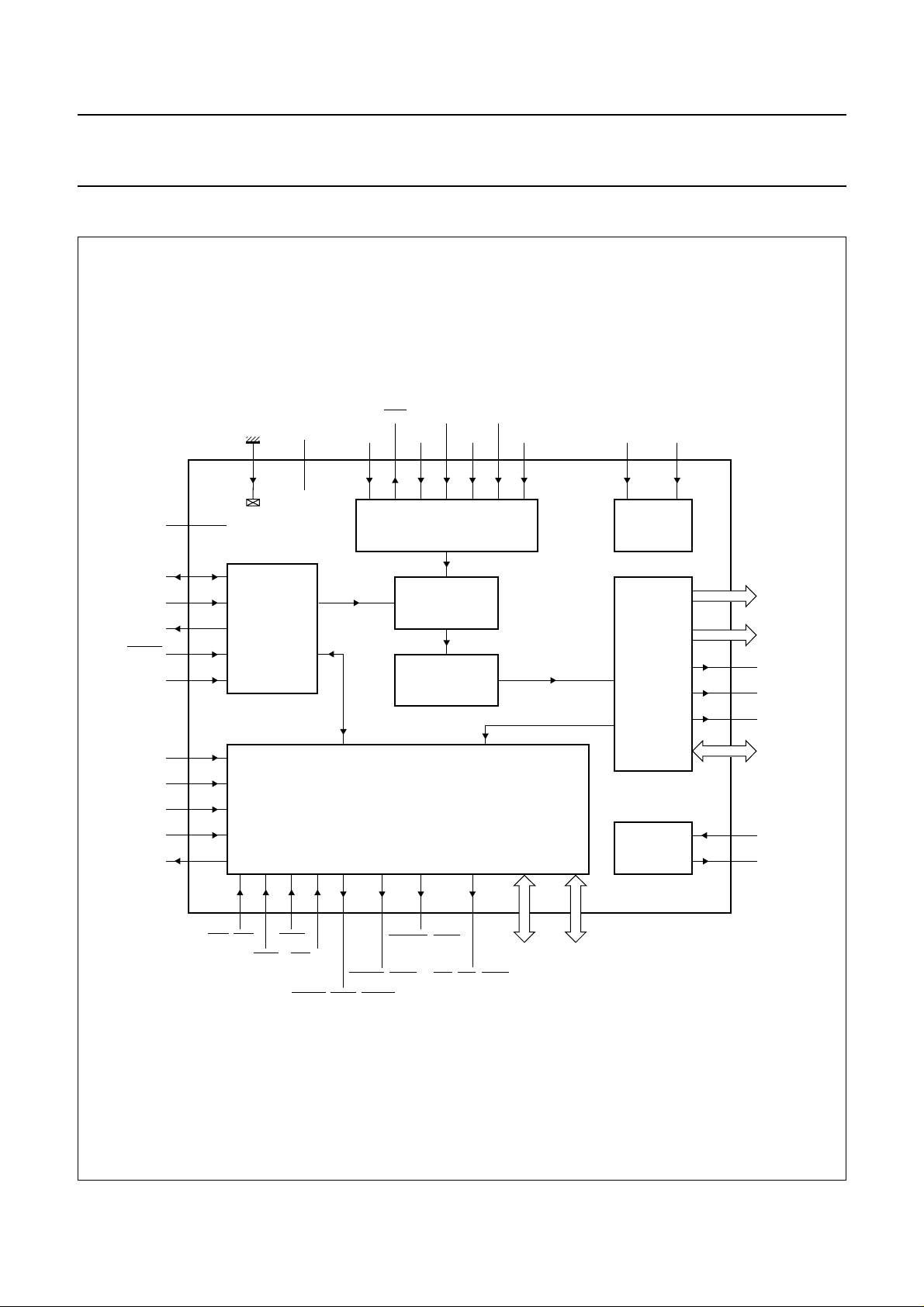
6 PINNING
SYMBOL PIN I/O DESCRIPTION
DGND1 1 − digital ground 1
RA6 2 O buffer RAM address bus output line 6
RA7 3 O buffer RAM address bus output line 7
RA8 4 O buffer RAM address bus output line 8
RA9 5 O buffer RAM address bus output line 9
RA10 6 O buffer RAM address bus output line 10
RA11 7 O buffer RAM address bus output line 11 (SRAM) only
RA12 8 O buffer RAM address bus output line 12 (SRAM) only
RA13 9 O buffer RAM address bus output line 13 (SRAM) only
RA14 10 O buffer RAM address bus output line 14 (SRAM) only
RA15/RAS 11 O buffer RAM address bus output line 15 (SRAM) or RAS (DRAM)
RA16/CAS 12 O buffer RAM address bus output line 16 (SRAM) or CAS (DRAM)
RWE 13 O buffer RAM write enable output
DGND2 14 − digital ground 2
RD0 15 I/O buffer RAM data bus bidirectional line 0
RD1 16 I/O buffer RAM data bus bidirectional line 1
RD2 17 I/O buffer RAM data bus bidirectional line 2
RD3 18 I/O buffer RAM data bus bidirectional line 3
RD4 19 I/O buffer RAM data bus bidirectional line 4
RD5 20 I/O buffer RAM data bus bidirectional line 5
RD6 21 I/O buffer RAM data bus bidirectional line 6
RD7 22 I/O buffer RAM data bus bidirectional line 7
TEST2 23 I test input 2
DGND3 24 − digital ground 3
TEST1 25 I test input 1
CROUT 26 O clock oscillator output
CRIN 27 I clock oscillator input
SFSY 28 I serial subcode input frame sync input
RCK 29 O serial subcode clock output (active LOW)
SUB 30 I serial input for Q-to-W subcode input
BCK 31 I serial interface bit clock input
V
DDD1
WS 33 I serial interface word clock input
DATA 34 I serial data input
C2PO 35 I serial interface flag input
SDA 36 I/O sub-CPU serial data input/output
SCL 37 I sub-CPU serial clock input
INT 38 O sub-CPU open-collector interrupt output
RESET 39 I power-on reset input (active LOW)
SYN 40 I sync signal input from sub-CPU
32 − digital supply voltage 1 (3.3 V)
1996 Apr 26 5
Page 6

Philips Semiconductors Preliminary specification
Error correction and host interface IC for
SAA7388
CD-ROM (ELM)
SYMBOL PIN I/O DESCRIPTION
DGND4 41 − digital ground 4
CS1/HEN 42 I host interface enable input (active LOW)
HWR 43 I host interface write enable input (active LOW)
HRD 44 I host interface read enable input (active LOW)
DMACK 45 I DMA acknowledge input
IORDY/WAIT/HFBLB 46 O host interface wait output (active LOW); 3-state control
SCRST/STEN 47 O host interface status enable output ATAPI sub-CPU reset signal
(active LOW)
DMARQ/DTEN 48 O ATAPI DMA request host interface data enable output (active LOW);
3-state control
IRQ/EOP/HFBC 49 O host interface end of process flag output ATAPI host interrupt request
(active LOW); 3-state control
V
DDD2
HD0 51 I/O host interface data bus input/output line 0
HD1 52 I/O host interface database input/output line 1
HD2 53 I/O host interface database input/output line 2
HD3 54 I/O host interface data bus input/output line 3
HD4 55 I/O host interface data bus input/output line 4
HD5 56 I/O host interface data bus input/output line 5
HD6 57 I/O host interface data bus input/output line 6
HD7 58 I/O host interface data bus input/output line 7
DGND5 59 − digital ground 5
HD8 60 I/O host interface data bus input/output line 8
HD9 61 I/O host interface data bus input/output line 9
HD10 62 I/O host interface data bus input/output line 10
HD11 63 I/O host interface data bus input/output line 11
HD12 64 I/O host interface data bus input/output line 12
HD13 65 I/O host interface data bus input/output line 13
HD14 66 I/O host interface data bus input/output line 14
HD15 67 I/O host interface data bus input/output line 15
DGND6 68 − digital ground 6
DA0/CMD 69 I host interface data input (active LOW)/command select input host interface
DA1 70 I ATAPI address line input 1
DA2/EJECT 71 I ATAPI address line input 2
CS2/SELRQ 72 I ATAPI chip select input 2
IOCS16 73 O ATAPI 16-bit data select output
V
DDD2
RA0 75 O buffer RAM address bus output line 0
RA1 76 O buffer RAM address bus output line 1
RA2 77 O buffer RAM address bus output line 2
50 − digital supply voltage 2 (5 V)
address line 0
74 − digital supply voltage 2 (5 V)
1996 Apr 26 6
Page 7
Philips Semiconductors Preliminary specification
Error correction and host interface IC for
CD-ROM (ELM)
SYMBOL PIN I/O DESCRIPTION
RA3 78 O buffer RAM address bus output line 3
RA4 79 O buffer RAM address bus output line 4
RA5 80 O buffer RAM address bus output line 5
handbook, full pagewidth
RA0
75
DDD2
V
IOCS16
74
73
SAA7388
CS2/SELRQ
DA2/EJECT
71
72
DA1
70
DA0/CMD
69
DGND1
RA6
RA7
RA8
RA9
RA10
RA11
RA12
RA13
RA14
RA15/RAS
RA16/CAS
RWE
DGND2
RD0
RD1
RD2
RD3
RD4
RD5
RD6
RD7
TEST2
DGND3
RA2
RA5
RA4
RA3
80
79
78
1
2
3
4
5
6
7
8
9
10
11
12
13
14
15
16
17
18
19
20
21
22
23
24
RA1
77
76
DGND6
68
HD15
67
HD14
66
HD13
65
HD12
64
HD11
63
HD10
62
HD9
61
HD8
60
DGND5
59
HD7
58
HD6
57
HD5
56
HD4
55
HD3
54
HD2
53
HD1
52
HD0
51
V
50
DDD2
IRQ/EOP/HFBC
49
DMARQ/DTEN
48
SCRST/STEN
47
IORDY/WAIT/HFBLB
46
DMACK
45
HRD
44
HWR
43
CS1/HEN
42
DGND4
41
SAA7388
25
26
27
28
29
30
31
32
SUB
TEST1
CRIN
CROUT
SFSY
RCK
BCK
V
Fig.2 Pin configuration.
1996 Apr 26 7
DDD1
33
WS
34
DATA
35
C2PO
36
SDA
37
SCL
38
INT
39
RESET
40
SYN
MGD306
Page 8

Philips Semiconductors Preliminary specification
Error correction and host interface IC for
CD-ROM (ELM)
6.1 Pin functions
6.1.1 RA0
External memory address signals.
6.1.2 RA16/CAS
External memory RA16 signal if SRAM or, CAS signal if
DRAM.
6.1.3 RA15/RAS
External memory RA15 signal if SRAM or, RAS signal if
DRAM.
6.1.4 RWE
Write output enable signal for external buffer memory. This
is LOW when the SAA7388 wants to write data into the
external memory.
6.1.5 RD0
External buffer memory bidirectional data signals.
TO RA14
TO RD7
SAA7388
6.1.12 C2PO
Error flag from the CD decoder. A HIGH indicates that a
byte has not been corrected by the C2 error corrector and
therefore is not valid. This is taken into account by the
SAA7388 error corrector.
6.1.13 SDA
Sub-CPU bidirectional data signal. This signal forms part
of the 3-wire serial interface between the SAA7388 and the
sub-CPU.
6.1.14 SCL
Sub-CPU sync signal. This signal forms part of the 3-wire
serial interface between the SAA7388 and the sub-CPU.
This signal is used to synchronize data transfers between
the sub-CPU and the SAA7388.
6.1.15 INT
Sub-CPU interrupt signal. This active LOW output signals
to the sub-CPU that the SAA7388 has an interrupt request.
6.1.6 SFSY
Frame sync for the Q-to-W subcode, indicates when
P-channel is available by a HIGH-to-LOW transition.
Frame 0 is also indicated by no transition on this line.
6.1.7
In response to SFSY going LOW data is clocked into the
SAA7388 before each rising edge using this clock output.
6.1.8 SUB
Q-to-W subcode is input in response to
mode or WS in “V4” mode compatible with the SAA7345.
6.1.9 BCK
Bit clock for the serial data input from the CD decoder.
6.1.10 WS
Word clock for the serial data input from the CD decoder.
6.1.11 DATA
Serial data input from the CD decoder. This may be either
2
I
S-bus or EIAJ 16-bit format.
RCK
RCK in 3-wire EIAJ
6.1.16
Forcing this input LOW resets the SAA7388.
6.1.17 SYN
Sub-CPU clock signal. This signal forms part of the 3-wire
serial interface between the SAA7388 and the sub-CPU.
This signal is the sub-CPU driven bit clock used to
synchronize the signals on the SDA line.
6.1.18
In the ATAPI mode this is the host chip select 1 address
signal. In the Sanyo and Oak compatibility modes setting
this input LOW enables the host interface.
6.1.19
This active LOW signal is the host write request.
6.1.20
This active LOW signal is the host read request.
RESET
CS1/HEN
HWR
HRD
1996 Apr 26 8
Page 9

Philips Semiconductors Preliminary specification
Error correction and host interface IC for
CD-ROM (ELM)
6.1.21 DMACK
This signal is used in the ATAPI and Oak compatibility
modes during DMA transfers. The host pulls this signal
LOW in response to a DMARQ request to indicate that it is
ready to transfer data.
If this signal is not being used then it must be pulled HIGH
for SAA7388 to operate correctly.
6.1.22
In the ATAPI mode this signal is negated to extend the
host transfer cycle of any host register access. It is used in
PIO transfers. When IORDY is not negated it is in a
high-impedance state.
In the Sanyo compatibility mode the function of this signal
depends on the SELRQ input. If SELRQ is HIGH then
WAIT is set LOW to extend the host transfer cycle. If
SELRQ is LOW then WAIT acts as the DRQ signal in a
DMA transfer.
IORDY/WAIT/HFBLB
SAA7388
6.1.25
In the ATAPI mode this active HIGH signal indicates a host
interrupt request. It is asserted when the sub-CPU writes
to the ITRG register and is negated when the host reads
the status register or writes to the command register.
In the Sanyo compatibility mode this signal is set LOW
when the last data byte is transferred to or from the host.
In the Oak compatibility mode this is the Host First Byte
Cycle output and is HIGH while the first byte in the pseudo
16-bit DMA transfer is accessed. It should be used to
inhibit non-DMA transactions while the first byte is latched.
6.1.26 HD0
These are the bidirectional Host Data signals. In the Sanyo
and Oak compatibility modes HD8 to HD15 are never
used.
6.1.27
IRQ/EOP/HFBC
TO HD15
DA0/CMD
In the Oak compatibility mode this signal is the Host First
Byte Latch signal. A rising edge on this signal is used to
latch the first byte in a pseudo 16-bit DMA read. HFBLB
can only be HIGH when pseudo 16-bit DMA transfer mode
is selected.
6.1.23
In the ATAPI or Oak compatibility mode this signal is pulled
LOW to reset the sub-CPU in response to a reset
command from the host.
In the Sanyo compatibility mode this signal is pulled LOW
to signal to the host that status bytes are available for
transfer.
6.1.24
In the ATAPI or Oak compatibility mode this signal is
asserted when the SAA7388 is ready to transfer data
between the host and itself. In ATAPI single word and Oak
DMA transfers this occurs at every word. In ATAPI
multi-word DMA transfers this occurs at the start of the
transfer.
In the Sanyo compatibility mode this signal is pulled LOW
to signal to the host that data bytes are available for
transfer.
SCRST/STEN
DMARQ/DTEN
In the ATAPI mode this is the host Data Address 0 signal.
In the Sanyo and Oak compatibility modes this input
selects between command or data transfers.
6.1.28 DA1
This is the ATAPI Data Address 1 signal.
6.1.29 DA2/ EJECT
In the ATAPI mode this is the Data Address 2 signal. In the
Oak compatibility mode this is the door switch input pin. Its
state is reflected in the TSTAT register.
6.1.30 CS2/SELRQ
In the ATAPI mode this is the Chip Select 2 signal. In the
Oak and Sanyo compatibility mode this is the data transfer
mode select input. It is used to select between PIO and
DMA transfers.
6.1.31 IOCS16
This open-collector signal is used in the ATAPI mode to
signal to the host that a 16-bit data port has been
addressed. It is not activated during DMA transfers.
1996 Apr 26 9
Page 10

Philips Semiconductors Preliminary specification
Error correction and host interface IC for
CD-ROM (ELM)
7 FUNCTIONAL DESCRIPTION
The SAA7388 is comprised of four main blocks; a CD
player interface, an error corrector, a host interface and a
memory manager. These four blocks operate in parallel.
All receive and send data to the buffer memory via the
memory manager. A 36-kbit on-chip SRAM has been
incorporated to allow high-speed data read operations for
the error corrector.
The SAA7388 performs simultaneous data input buffering,
error correction and host data transfer.
7.1 CD-DSP interface and data input
The input data is synchronized, decoded, and written to
the buffer RAM. The input data format is software
programmable.
The synchronization is achieved using a sync detector and
a sync interpolator. The sync detector detects the sync
pattern in every sector while the interpolator avoids sync
loss when no sync is found. The detector and interpolator
can be individually enabled and disabled under software
control.
After decoding, each full sector of data (2352 bytes)
comprising sync, header, sub-header and parity fields is
written to the buffer RAM.
7.2 Error correction and EDC check
Error correction and detection is performed on each sector
after it is written to the buffer RAM.
SAA7388
7.3 Host interface
The host interface controls data transfers between the
SAA7388 and an external microcontroller. The host
interface can be programmed to operate in three modes.
In the Sanyo compatibility mode the host interface is
functionally compatible with the Sanyo LC89510 block
decoder. In the Oak compatibility mode the host interface
is functionally compatible with the Oak OTI-012 controller
chip in enhanced mode.
In the ATAPI mode the interface meets the ATA Program
Interface specification.
7.4 Subcode channel Q-to-W buffering
As well as buffering the main data, the SAA7388 can also
be used to buffer R-to-W subcode data in buffer memory.
Two buffer modes exist, raw mode and cooked mode. In
the raw mode, data is written to an external RAM without
any processing being performed. In the cooked mode, the
Q-channel data is extracted, the Q-channel CRC is
calculated, the R-to-W data is de-interleaved and the
residues of each R-to-W frame are calculated. These
residues make it easier to correct errors in the data.
7.5 External buffer memory
It is possible to use the SAA7388 with different external
RAM memories. From 0 to 128 kbyte SRAMs or to 16-Mbit
DRAMs are possible. Memories may be nibble or byte
wide (allowing 2, 8 or 16 Mbits). Selection is performed
under software control.
The SAA7388 buffers flag and data of sectors to be
corrected in a 9-bit, 4096 words on-chip RAM memory.
For erasure correction, no external 9-bit memory is
required.
The standard error correction algorithm can be
programmed, and supports mode 1 and mode 2 form 1
and form 2 discs.
After error correction, an electronic data check is
executed.
When this EDC check is also complete, the sector header
and sub-header is written to 8 header registers, and a
decode complete interrupt is generated.
The microcontroller can then read the decoder status, the
sector header and sub-header and the sector start
address from the SAA7388.
1996 Apr 26 10
Unique to the SAA7388 is its ability to work with partly
defective DRAMs. The SAA7388 offers the possibility to
use a DRAM with bytes in error.
A RAM test is executed under microcontroller control. This
RAM test indicates defective segments to the
microcontroller which keeps a list of which bad sectors to
avoid. The list can be stored in the buffer memory and/or
the microcontrollers own memory.
7.6 Sub-CPU registers
This section describes the registers in the SAA7388. The
operation of the registers varies depending on whether
they are being read from or written to, and the host mode
selected.
Page 11
Philips Semiconductors Preliminary specification
Error correction and host interface IC for
SAA7388
CD-ROM (ELM)
Table 1 Sub-CPU registers during write
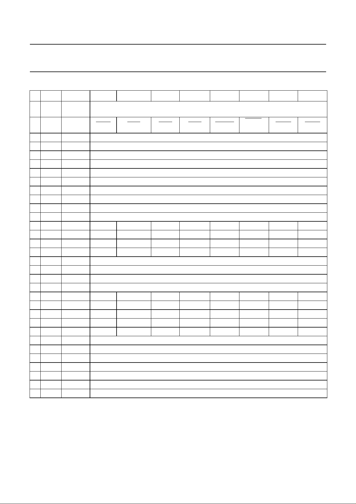
# AR NAME BIT 7 BIT 6 BIT 5 BIT 4 BIT 3 BIT 2 BIT 1 BIT 0
0 00000
1 00001 IFCTRL CMDIEN DTEIEN DECIEN CMDBK DTWAI STWAI DOUTEN SOUTEN
2 00010 DBCL Data Byte Count register bits 7 to 0
3 00011 DBCH Data Byte Count register bits 15 to 8
4 00100 DACL Data Address Counter register bits 7 to 0
5 00101 DACH Data Address Counter register bits 15 to 8
6 00110 DTRG Data Transfer Trigger register
7 00111 DTACK Data Transfer Acknowledge register
8 01000 WAL Write Address register bits 7 to 0
9 01001 WAH Write Address register bits 15 to 8
10 01010 CTRL0 DECEN lookahead E01RQ AUTOQ ERAMRQ WRRQ ECCRQ ENCODE
11 01011 CTRL1 SYIEN SYDEN DSCREN COWREN MODRQ FORMRQ MBCKRQ SHDREN
12 01100 PTL Block Pointer register bits 7 to 0
13 01101 PTH Block Pointer register bits 15 to 8
14 01110
15 01111
16 10000 DACHH mem Data Address Counter register bits 20 to 16
17 10001 WAHH Write Address register bits 20 to 16
18 10010 PTHH Block Pointer register bits 20 to 16
19 10011 SUB_L Subcode Address register bits 7 to 0
20 10100 SUB_H Subcode Address register bits 9 and 8
21 10101
22 10110 INCNF IISmode div 1 div 0 QWmode QWon QWcook RAM test 0
23 10111 MEMS 0 PRIORITY 0 RFRSH WIDTH STATIC CACHE
24 11000 ASTAT ATAPI Status register
25 11001 ITRG Host Interrupt Trigger register
26 11010 ADRADR ATAPI Drive Address register
27 11011 ASAMT ATAPI SAM TAG register
28 11100 DTCTR res. DMAMODE UDMA SUBIEN RDRV TRANT
29 11101 ADRSEL ATAPI Drive Select register
30 11110 AINTR ATAPI Interrupt Reason register
31 11111 AERR ATAPI Error register
ADATA/
SBOUT
RESET reserved HSEL
ATAPI Data register/Status Byte Output register
1996 Apr 26 11
Page 12
Philips Semiconductors Preliminary specification
Error correction and host interface IC for
SAA7388
CD-ROM (ELM)
Table 2 Sub-CPU registers during read
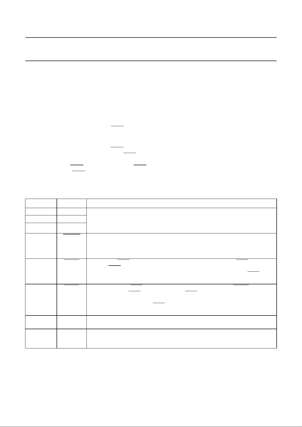
# AR NAME BIT 7 BIT 6 BIT 5 BIT 4 BIT 3 BIT 2 BIT 1 BIT 0
0 00000
1 00001 IFSTAT CMDI DTEI DECI SUBI DTBSY
2 00010 DBCL Data Byte Count register bits 7 to 0
3 00011 DBCH Data Byte Count register bits 15 to 8
4 00100 HEAD0 Minutes/ File Number
5 00101 HEAD1 Seconds/ Channel Number
6 00110 HEAD2 Frames/ Submode
7 00111 HEAD3 Mode/ Coding Information
8 01000 PTL Block Pointer register bits 7 to 0
9 01001 PTH Block Pointer register bits 15 to 8
10 01010 WAL Write Address register bits 7 to 0
11 01011 WAH Write Address register bits 15 to 8
12 01100 STAT0 CRCOK ILSYNC NOSYNC LBLK USHORT SBLK ERR UCEB
13 01101 STAT1 MINERR SECERR BLKERR MODERR SH0ERR SH1ERR SH2ERR SH3ERR
14 01110 STAT2 RMOD3 RMOD2 RMOD1 RMOD0 MODE FORM RFORM1 RFORM2
15 01111 STAT3 VALST CBLK
16 10000 PTHH Block Pointer register bits 20 to 16
17 10001 WAHH Write Address register bits 20 to 16
18 10010 SUB_L Subcode Address register bits 7 to 0
19 10011 SUB_H Subcode Address register bits 9 and 8
20 10100
21 10101
22 10110
23 10111
24 11000
25 11001 HCON Oak Host Configuration register
26 11010 ACMD ATAPI Command register
27 11011 ASAMT ATAPI SAM TAG register
28 11100 ADCTR ATAPI Device Control register
29 11101 ADRSEL ATAPI Drive Select register
30 11110 AINTR ATAPI Interrupt Reason register
31 11111 AFEAT ATAPI Features register
APCMD/
COMIN
ATAPI packet command data/command input register
SRSTI/
STBSY
DTEN STEN
1996 Apr 26 12
Page 13
Philips Semiconductors Preliminary specification
Error correction and host interface IC for
CD-ROM (ELM)
7.7 Register Descriptions
7.7.1 SBOUT/ADATA
This is a 12 byte FIFO used to transfer data from the
sub-CPU to the host.
In the Sanyo and Oak compatibility mode writing to this
register starts a status byte transfer. In this mode if the
SOUTEN bit in the IFCTRL register has been set to logic 1,
writing to the SBOUT register sets the STBSY bit to
logic 0. If the STWAI bit is set to logic 0,
immediately set LOW to inform the host computer that the
status byte is ready to be read from.
If the STWAI bit is set to logic 1 and the DTEN bit in the
IFSTAT register is also set to logic 1, both the STEN pin
and the STBSY will go LOW. However, if the STWAI bit is
set to logic 0, and theDTEN bit is set to logic 0, thenSTEN
is held HIGH until the DTEN bit goes HIGH, thereafter it
goes LOW.
STEN is
SAA7388
7.7.2 COMIN/ APCMD
During the ATAPI mode this register is used to read the
program command sent by the host. The program
command can only be received if the appropriate mode
has been selected (see Table 22) and a data transfer has
been started (see DTRG register).
During Sanyo and Oak compatibility modes this register is
a 12 byte FIFO which is used to transfer commands from
the host to the sub-CPU. If reading this register empties
the command FIFO then CMDI is set to logic 1 and further
reads from the register will return FFH.
7.7.3 IFCTRL
The IFCTRL register provides control over the host
interface. Resetting the chip will clear all bits. In the ATAPI
mode, only, bits 7 to 5 have any effect.
Table 3 IFCTRL register bits
BIT NAME DESCRIPTION
7 CMDIEN Enable bits for CMDI, DTEI and DECI. These are interrupt masks, enabling/disabling the
6 DTEIEN
5 DECIEN
4
3
2
1 DOUTEN Data output enable. DOUTEN enables/disables data transfers. When set to logic 0, all
0 SOUTEN Status output enable. SOUTEN enables/disables status byte transfers. When set to
CMDBK Command break enable. If set to logic 0 then the command break function is enabled
DTWAI Data transfer WAIT enable. Setting this bit to logic 0 enables the data WAIT function.
STWAI Status byte transfer WAIT enable. This bit acts in a similar way to the DTWAI bit except it
sub-CPU interrupt pin. They do not affect the bits in the IFSTAT register. If set to logic 1,
the corresponding interrupt is enabled. It should be noted that these masks do not clear
the interrupts.
and if the host writes to the COMIN FIFO then any data or status byte transfers in
progress will be terminated. If set to logic 1 then this operation is disabled. The data
transfer interrupt DTEI is not generated by a command break.
The data WAIT function allows the SAA7388 to delay hardware execution of the data
transfer until a status byte transfer has been completed. Disabling the data WAIT
function allows data transfers to take place independently of status byte transfers.
controls the status WAIT function. The status WAIT function allows the SAA7388 to
delay hardware execution of the status transfer until a data byte transfer has been
completed. Disabling the data WAIT function allows status transfers to take place
independently of data transfers.
data transfers in progress are aborted.
logic 0, the status FIFO register is reset to empty and all status byte transfers in progress
are aborted.
1996 Apr 26 13
Page 14
Philips Semiconductors Preliminary specification
Error correction and host interface IC for
SAA7388
CD-ROM (ELM)
7.7.4 IFSTAT
The IFSTAT register indicates the state of the host interface. In the ATAPI mode, only bits 7 to 2 have any meaning.
Table 4 IFSTAT register bits
BIT NAME DESCRIPTION
7
6
5
4
3
2
1
0
CMDI Command interrupt. In the ATAPI mode this bit is asserted when the host has written
to the ATAPI command register (see ACMD register) and the drive is selected. It is
also asserted when the host writes the execute drive diagnostic command (90H) to
the ATAPI command register, regardless of whether the drive is selected. It is
negated when the sub-CPU reads the ACMD register. In the Sanyo and Oak
compatibility modes this bit is asserted while there are command bytes waiting in the
COMIN FIFO. It is negated when the COMIN FIFO is empty.
DTEI Data transfer end interrupt. This bit is asserted at the end of data transfer. It is
negated when the sub-CPU writes to the DTACK register. If the ATAPI mode is
selected this bit is also asserted when a program command has been received and
after a sub-CPU memory transfer.
DECI Decoder interrupt. This bit is asserted when a new sector is available. It is negated by
reading the STAT3 register.
SUBI Subcode interrupt. This bit is asserted when a new subcode is available. It is negated
by reading the SUB_H register.
DTBSY Data transfer busy.This bit indicates if a data transfer is taking place. It is asserted by
writing to the DTRG register and is negated at the end of the transfer.
SRSTI/STBSY SRST bit interrupt/status transfer busy. In the ATAPI mode this bit is asserted when
the host writes to the ATAPI device control register and sets the SRST bit. It is
negated when the sub-CPU reads the ADCTR register. It should be noted that if this
bit is asserted in the ATAPI mode then the sub-CPU interrupt will also be asserted.
The SRSTI interrupt cannot be disabled. In the Sanyo and Oak compatibility modes
this bit indicates if a status byte transfer is taking place. It is asserted by writing to the
SBOUT register and is negated when the host has emptied the status FIFO.
DTEN Data transfer and status transfer. These bits reflect the state of the DTEN and STEN
STEN
pins in the Sanyo and Oak compatibility modes. They are updated at the end of a
host read or write.
7.7.5 DBCL AND DBCH
The Data Byte Counter is used by the sub-CPU to control
the number of bytes that are transferred in a data transfer.
In the ATAPI mode all 16 bits are available while in the
Sanyo and Oak compatibility modes only 15 bits are
available with bit 7 of DBCH indicating the state of DTEI
(see Table 4). During memory-to-host data transfers the
data byte counter is decremented after every host read.
During host-to-memory data transfers the data byte
counter is decremented as data is written into external
buffer memory.
1996 Apr 26 14
7.7.6 DACL, DACH AND DACHH
This 21-bit write-only register is used to specify the
external buffer address of the first byte of the data block to
be transferred to the host.
Once the address has been set, it is incremented
automatically as successive bytes are transferred with the
host. It should be noted that pointer operation is
asynchronous from host read/write operation. For this
reason, counter increments are not coincident with host
transfer operations.
Page 15

Philips Semiconductors Preliminary specification
Error correction and host interface IC for
CD-ROM (ELM)
Bit 7 of the DACHH register specifies which memory is
accessed. If the bit is clear then the address refers to the
external memory, if the bit is set then the address refers to
the 4 kbyte internal memory. The internal memory should
not be accessed during error correction.
This register should be written to before each data transfer
because its value will be undefined at the end of the
previous transfer.
7.7.7 PTL, PTH
This register holds a 21-bit pointer to the external buffer
memory address of the head of the current data block after
correction.
The SAA7388 defines the minute byte in the header to be
at the head of the block, and the 12 sync bytes at the tail
of the block. Each block contained in the buffer is taken to
be 2352 bytes.
The controller can transfer the decoded block back to the
host by copying the address of this register to the DACL,
DACH and DACHH pointers after a decoder interrupt.
When the WRRQ bit in the CTRL0 register is set to logic 1,
this pointer is updated at the sync signal of every
2352 byte clocks.
7.7.8 WAL, WAH
These registers contain a 21-bit address of where raw data
from the drive is written to the external buffer memory. The
pointer is automatically incremented during data transfer.
The pointer should only be read while drive data writes to
the buffer are disabled. If WAHH is written to while drive
data write is enabled, then the new WA value will be used
AND PTHH
AND WAHH
SAA7388
for the first byte of the next sector. The new pointer value
is temporarily stored in the PT register. This cannot be
read after WA has been written to.
7.7.9 DTRG
Writing to this register starts a data transfer. The data
written is discarded.
7.7.10 DTACK
Writing to this register clears the
written is discarded.
7.7.11 HEAD0, HEAD1, HEAD2
These registers are used to hold the header and the
sub-header data of the current block.
To read the header data set, the SHDREN bit in the
CTRL1 register is set to logic 0; to read the sub-header
data, SHDREN is set to logic 1.
If sub-header is selected, the registers will normally hold
data from bytes 20 to 23. However, if the error flag for one
of these bytes is set, then the byte is taken from the first
sub-header field. (bytes 16 to 19.)
The error flags for header and sub-header can be read
from the STAT1 register. No error correction is performed
on header or sub-header.
Header and sub-header registers are valid directly after
decoder interrupt, and as long as the VALST bit in the
STAT3 register is LOW. In all write modes they contain
information on the block whose header is pointed to by
PTL, PTH and PTHH.
DTEI interrupt. The data
AND HEAD3
Table 5 HEAD registers
SHDREN REGISTER CONTENTS
0 HEAD0 MINUTES (byte12)
0 HEAD1 SECONDS (byte 13)
0 HEAD2 FRAMES (byte 14)
0 HEAD3 MODE (byte 15)
1 HEAD0 FILE NUMBER (byte 16 or 20)
1 HEAD1 CHANNEL NUMBER (byte 17 or 21)
1 HEAD2 SUBMODE NUMBER (byte 18 or 22)
1 HEAD3 CODING INFORMATION (byte 19 or 23)
1996 Apr 26 15
Page 16

Philips Semiconductors Preliminary specification
Error correction and host interface IC for
CD-ROM (ELM)
7.7.12 CTRL0
Resetting the chip sets all the bits in this register to logic 0.
Table 6 CTRL0 register
BIT NAME FUNCTION
7 DECEN Disable decoding = 0; Enable decoding = 1. This bit enables/disables decoding
functions. Disabling the decoding functions also disables the decoder interrupt.
6 lookahead At interrupt PT, header refer to current block = 0; At interrupt PT, header refer to next
block = 1. When this bit is set to logic 1 at decoder interrupt, CMA and header registers
will give information on the next block instead of on the current block. The lookahead
mode was included to provide support for bad RAMs, and to give the CPU better control
on the blocks it wants to read.
5 E01RQ Disable error correction of bytes = 0; Enable correction of CIRC mis-corrections = 1.
Setting this bit to logic 0 instructs the error corrector not to correct bytes flagged as
reliable by the CIRC error corrector.
4 AUTORQ Disable automatic error correction = 0; Enable automatic error correction = 1. Requests
automatic extraction of form bit during mode2 correction from sub-header data.
3 ERAMRQ Disable erasure flag use = 0; Enable erasure flag use = 1. When set to logic 1, the
SAA7388 will enable the use of erasure flag information for error correction. When set to
logic 0, the SAA7388 will disable the use of erasure flag information for error correction.
Use of erasure flags must be disabledSAA7388 when the CD-DSP does not output
erasure flags and when the internal buffer RAM is disabled (which is necessary for
repeat correction).
2 WRRQ Disable data writes to the buffer and PTL updates = 0; Enables data writes to the buffer
and PTL updates = 1. This bit enables/disables writes from the CD drive into the buffer. It
also enables/disables pointer (PTL, PTH and PTHH) updates each time a block is
received. When WRRQ is set to logic 1, data write will start from the first byte of the next
block onwards. When WRRQ is set to logic 0, repeat correction is enabled. With WRRQ
set to logic 0, the internal buffer RAM is disabled.
1 ECCRQ Disable ECC correction = 0; Enable ECC correction = 1. When ECCRQ is set to logic 1
the blocks received by the SAA7388 will be error corrected before a decoder interrupt is
generated. When ECCRQ is set to logic 0 no corrections are performed. The algorithm
used is a QD, PD, QE, PE algorithm. In a first step, errors are corrected; in a second
step, erasures are corrected. Correction data is read from the on-chip 36 kbit buffer
memory.
0 ENCODE Normal operation = 0; Test mode, do not use = 1, this bit must always be set to logic 0.
SAA7388
1996 Apr 26 16
Page 17
Philips Semiconductors Preliminary specification
Error correction and host interface IC for
CD-ROM (ELM)
Table 7 Error correction modes
DECEN lookahead WRRQ ECCRQ decoder mode
0 X X X decoder disable; note 1
1000monitor only
1001repeat correction
1010write only
1011real-time correct, normal mode
1110write only, lookahead
1111real-time correct, lookahead
Note
1. Where X = don’t care.
7.7.13 CTRL1
The reset function clears all the flags in this register.
Table 8 CTRL1 register bits
SAA7388
BIT NAME FUNCTION
7 SYIEN Disable sync interpolation = 0; Enable sync interpolation = 1. Enabling SYIEN prevents
loss of synchronization when an error occurs in a sync pattern during data read.
6 SYDEN Disable sync detection = 0; Enable sync detection = 1. Enabling SYDEN synchronizes
the decoder with the sync pattern detected in the input data.
5 DSCREN Descramble disable (audio) = 0; Descramble enable = 1. This bit enables/disables
descrambling. Setting this bit to logic 0 allows reading of raw data on disc, even audio
signals. This bit should be set to logic 1 for CROM data.
4 COWREN CRC with error correction disabled = 0; Detection errors are corrected = 1. This bit
enables/disables rewriting of error bytes in the buffer during error correction. Setting
the bit to logic 0 allows CRC checks without error correction.
3 MODRQ Mode 1 request = 0; Mode 2 request = 1. This bit discriminates Mode 1/Mode 2.
2 FORMRQ Form 1 request = 0; Form 2 request = 1. This bit discriminates Mode 2/Form 1 and
Mode 2/Form 2.
1 MBCKRQ Disable mode check function = 0; Enable mode check function = 1. If the mode
specified in the mode byte does not correspond with the raw data mode bit and this bit
is set to logic 1 then error correction and detection is disabled.
0 SHDREN Header data on registers Head0 to Head3 = 0; Sub-header data on registers
Head0 to Head3 = 1. This bit toggles header and sub-header data between registers
HEAD0 to HEAD3.
1996 Apr 26 17
Page 18

Philips Semiconductors Preliminary specification
Error correction and host interface IC for
CD-ROM (ELM)
7.7.14 STAT0
Resetting the chip clears all bits in this register.
Table 9 STAT0 register bits
BIT NAME FUNCTION
7 CRCOK Cyclic redundancy check not OK = 0; Cyclic redundancy check OK = 1. Set by the
EDC in accordance with the results of the CRC check.
6 ILSYNC Sync pattern detected at word count 0 to 1174 or 1176 onwards = 1. This bit is set to
logic 1 if the sync pattern in the incoming data is detected between word counts
0 and 1174 or 1176 to infinity, and the decoder has been retimed. Due to the
presence of the cache RAM, it is necessary to stop error correction also when long
blocks have been detected.
5 NOSYNC Sync pattern inserted by sync interpolator not coincident with data sync = 1. This bit
is set to logic 1, if the word counter reaches 1175 and no sync pattern has been
detected in the input data. It indicates that the sync interpolator circuit inserted a
sync.
4 LBLK With SYIEN = 0, no sync found. Data block size has been extended = 1. This bit is
set to logic 1, if the sync interpolator was switched off, and if the sync interpolator
indicated that sync insertion was necessary. This condition causes the block length to
be extended.
3 Reserved
2 SBLK Short block indication = 1. This bit is set to logic 1 if the decoder is not retimed when
a sync pattern is detected in an incorrect word location, and is ignored while the
SYDEN bit is set to logic 0.
1 ERABLK One or more bytes of the block are flagged with C2 flags = 1. This bit is set to logic 1
if one or more bytes of the current block contain erasures as indicated by the C2PO
input.
0 UCEBLK Uncorrectable errors in block = 1. This bit is set to logic 1 when one or more bytes of
the current block remain in error after the error correction process.
SAA7388
7.7.15 STAT1
Resetting the chip clears all bits in this register.
The bits in this register indicate the reliability of data in the HEAD0 to HEAD3 registers. Bits MINERR, SECERR,
BLKERR and MODERR indicate errors in the minutes, seconds, frames and mode bytes in the header of the current
block. Bits SH0ERR to SH3ERR indicate errors in the respective bytes in the sub-header.
Table 10 STAT1 register bits
BIT 7 BIT 6 BIT 5 BIT 4 BIT 3 BIT 2 BIT 1 BIT 0
MINERR SECERR BLKERR MODER SH0ERR SH1ERR SH2ERR SH3ERR
1996 Apr 26 18
Page 19

Philips Semiconductors Preliminary specification
Error correction and host interface IC for
SAA7388
CD-ROM (ELM)
7.7.16 STAT2
The bits MODE and FORM in this register indicate the mode, form and correction scheme of the current frame.
Table 11 STAT2 register bits
BIT 7 BIT 6 BIT 5 BIT 4 BIT 3 BIT 2 BIT 1 BIT 0
RMOD3 RMOD2 RMOD1 RMOD0 MODE FORM RFORM1 RFORM2
Table 12 MODE and FORM bits
MODE FORM SETTING
0 0 Mode 1
1 0 Mode 2, Form 1
X 1 Mode 2, Form 2 or ECC correction impossible
The Mode bit is always copied from the CTRL1 register.
The Form information is determined by the AUTORQ bit in
the CTRL0 register. When this bit is set to logic 0, the Form
information is copied from the CTRL1 register. When this
bit is set to logic 1 the Form information is copied from the
Mode header byte.
If correction of the block was impossible, FORM will be set
to logic 1 regardless of the requested correction. This will
happen under the following circumstances:
• An illegally synchronized block (ILSYNC = 1 or
LBLK = 1)
• A data block specified as Mode 2, Form 2, or detected
as Mode 2, Form 2
• A Mode 2 submode byte error detected during
processing
• A mode mismatch detected by the mode check function
(MCHQRQ = 1)
• A mode byte error detected by the mode check function
(MCHQRQ = 1).
The RFORM2, RFORM1 bits contain a preview of the form
bit for the next frame
Table 13 RFORM2 and RFORM1 bits
RFORM1 RFORM2 MEANING
0 0 Form 0
0 1 Form 1
1 X error in form byte
The RMOD3, RMOD2, RMOD1 and RMOD0 bits contain
a preview of the next block MODE byte.
RMOD3 = bit7 # bit6 # bit5 # bit4 # bit3 # C2FLAG
RMOD2 = bit2 # C2FLAG
RMOD1 = bit1 # C2FLAG
RMOD0 = bit0 # C2FLAG
1996 Apr 26 19
Page 20

Philips Semiconductors Preliminary specification
Error correction and host interface IC for
CD-ROM (ELM)
Table 14 RMOD bits
RMOD3 RMOD2 RMOD1 RMOD0 MEANING
0000 mode 0
0001 mode 1
0010 mode 2
0011 mode 3
0100 mode 4
0101 mode 5
0110 mode 6
0111 mode 7
1 X X X mode > 7 or error in mode byte (note 1)
Note
1. Where X = don’t care.
7.7.17 STAT3
Reading this register clears any DECI interrupts.
SAA7388
Table 15 STAT3 register bits
BIT NAME MEANING
7 VALST Registers associated with decoder interrupt valid = 0; Registers invalid = 1. This bit is
a valid/invalid flag for the registers related to the decoder interrupt. After decoder
interrupt, the sub-CPU must read out of all decoder registers before VALST goes
HIGH.
6 −−
5 CBLK ECC not performed on current block = 0; ECC has been performed on current
block = 1. This bit will go to logic 1 if ECC correction has been performed on the
current block.
2 −−
1−−
0−−
7.7.18
Writing to this register resets the SAA7388 and initializes all of the registers. The data written determines the host mode
of SAA7388.
Table 16
RESET
RESET register bits
BIT 7 BIT 6 BIT 5 BIT 4 BIT 3 BIT 2 BIT 1 BIT 0
reserved HSEL
The HSEL bits in the
The SAA7388 will then wait until the sub-CPU writes to the RESET register and selects the host mode. After hardware
reset 3-statable pins will be 3-state unless HRD is driven LOW.
1996 Apr 26 20
RESET register set the host interface mode. After a hardware reset the HSEL bits become 111.
Page 21

Philips Semiconductors Preliminary specification
Error correction and host interface IC for
SAA7388
CD-ROM (ELM)
Table 17 HSEL bits
HSEL CONTENT
BIT 2 BIT 1 BIT 0
0 0 0 Sanyo Sanyo compatible mode
0 0 1 ATAPI ATAPI Mode
0 1 0 Oak Oak compatible mode
0 1 1 unknown host all host bus pins 3-state, default after h/w reset
others reserved for future enhancements
7.7.19 SUB_L, SUB_H
This 10-bit register specifies the memory address of the subcode data block. This address will always be in the first
1 kbyte of memory.
7.7.20 INCNF
This register is used to specify the configuration of the input data path.
Table 18 INCNF register bits
SELECTED HOST
INTERFACE
DESCRIPTION
BIT NAME DESCRIPTION
2
7 IISmode I
6 div1
5 div0
4 QWmode Selection of Q-to-W input format. Logic 0 = V4 mode; logic 1 = EIAJ mode.
3 QWon Q-to-W interface enable. Logic 0 = off; logic 1 = on.
2 QWcook Q-to-W interface cooking enable. Logic 0 = cooked mode; logic 1 = RAW mode.
1 RAMtest External RAM test mode. Logic 0 = normal operation; logic 1 = RAM test mode.
0 −−
Note
1. For subcode Q-to-W recovery, the BCK clock is used as a timing reference. It is possible to recover the Q-to-W
subcode using the SAA7388, while at the same time the serial interface is programmed in oversampling mode for a
DAC. Under such circumstances, it is necessary to tell the SAA7388 the oversampling factor.
(1)
(1)
S-bus mode = 0; EIAJ serial interface mode = 1.
If div1 and div0 = logic 0 then no oversampling (normal CDROM modes); If div1 = logic 0
and div0 = logic 1 then 2 times oversampling; If div1 = logic 1 and div0 = logic 0 then
4 times oversampling.
If div1 and div0 = logic 0 then no oversampling (normal CDROM modes); If div0 = logic 1
and div1 = logic 0 then 2 times oversampling; If div1 = logic 0 and div1 = logic 0 then
4 times oversampling.
1996 Apr 26 21
Page 22

Philips Semiconductors Preliminary specification
Error correction and host interface IC for
SAA7388
CD-ROM (ELM)
7.7.21 MEMS
This register is used to specify the configuration of the external buffer memory.
Table 19 MEMS register bits
BIT NAME DESCRIPTION
7
6 PRIORITY Host priority access. These bits specify the external memory accesses priority.
5 PRIORITY
4 −−
3 RFRSH DRAM refresh rate. Setting this bit specifies a DRAM refresh rate of clock
frequency/400. Clearing this bit specifies a rate of clock frequency/200. WIth a 33 MHz
clock this bit should be set, while with a 16 MHz clock the bit should be clear.
2 WIDTH DRAM width select. This bit should be set if the external DRAM has a nibble wide data
bus. If the data bus is byte wide then this bit should be clear.
1 STATIC SRAM/DRAM select. If the external buffer memory is DRAM then this bit should be
cleared. If the memory is SRAM this bit should be set.
0 CACHE CACHE memory select. If the internal cache is available then this bit should be clear.
Setting this bit to logic 1 indicates that there is no internal cache memory.
Table 20 Host priority access
PRIORITY BITS
BIT 6 BIT 5
0 0 only one host access has highest priority
0 1 two successive host accesses have highest priority
1 0 three successive host accesses have highest priority
1 1 four successive host accesses have highest priority
7.7.22 ITRG
In the ATAPI mode writing to this register generates a host
interrupt. This interrupt is cleared when the host reads the
ATAPI status register or writes to the ATAPI command
register.
In the Sanyo and Oak compatibility modes writing to this
register has no effect.
7.7.23 ASTAT
This write only register is only available in the ATAPI
mode; it is the ATAPI status register and is used to transfer
status information to the ATAPI host.
Bit 7 of this register is the BSY bit and this is set by the
SAA7388 whenever;
• SAA7388 is the selected drive and the host writes to the
command register (ACMD)
• The host writes the execute drive diagnostic command
(90H) to the command register
• The host writes to the device control register (ADCTR)
and sets the SRST bit
• There is a hardware reset.
On reset this register is set to (80H).
ACCESS
1996 Apr 26 22
Page 23

Philips Semiconductors Preliminary specification
Error correction and host interface IC for
SAA7388
CD-ROM (ELM)
7.7.24 ACMD
This read only register is only available in the ATAPI mode;
it is the ATAPI command register and is used to transfer
commands from the host to the SAA7388.
The CMDI interrupt is generated when;
• The host writes to this register while the SAA7388 is the
selected drive (the DRV bit in the ADRSEL register is
equal to the RDRV bit in the DTCTR register)
• The host writes the execute drive diagnostic command
(90H) to this register.
The BSY bit in the ASTAT register is also set under these
conditions. If the sub-CPU reads this register while CMDI
is asserted then it will be negated.
7.7.28 ADRSEL
Table 21 ADRSEL register bits
BIT 7 BIT 6 BIT 5 BIT 4 BIT 3 BIT 2 BIT 1 BIT 0
111DRV−−−−
7.7.25 ADRADR
This write only register is the ATAPI Drive Address
register.
7.7.26 ASAMT
This register is the ATAPI Sector Number register.
7.7.27 ADCTR
This read only register is the ATAPI Device Control
register. If the SRSTI interrupt is asserted then reading this
register will negate it.
Bit 4 of this register is the DRV bit. When this bit is the same as the RDRV bit in the DTCTR register then the SAA7388
will be the selected ATAPI drive and will respond to host commands and produce host interrupts.
7.7.29 AINTR
This register is the ATAPI Interrupt Reason register.
7.7.30 AFEAT
This read only register is the ATAPI Features register.
7.7.31 AERR
This write only register is the ATAPI Error register.
7.7.32 DTCTR - D
The DTCTR register controls data transfer flows in the host
Interface block. On reset this register is cleared to all zeros
except for the RDRV bit which is set to logic 1. This means
that the SAA7388 will be set to drive 1 after a reset.
There are several possible data transfers through the
SAA7388 host Interface block and these are selected
using the TRANT bits. The transfers are described in the
Table 23.
ATA TRANSFER CONTROL REGISTER
1996 Apr 26 23
Page 24

Philips Semiconductors Preliminary specification
Error correction and host interface IC for
SAA7388
CD-ROM (ELM)
Table 22 Data transfer control register bits
BIT FLAG VERBOSE DESCRIPTION
7 res. − reserved
6 DMAMODE DMA Mode Select logic 0 = single-word; logic 1 = multi-word
5 UDMA Use DMA logic 1 = DMA; logic 0 = PIO
4 SUBIEN SUBI Enable logic 1 = interrupt enabled
3 RDRV Real Drive Select ATAPI drive number
2 TRANT − see Table 23
1
0
Table 23 TRANT transfer bits
TRANT
BIT 2 BIT 1 BIT 0
0 0 0 memory host 65535 (ATAPI) DMA and PIO
0 0 1 host memory 65535 (ATAPI) DMA and PIO
0 1 0 sub-CPU memory −−
0 1 1 memory sub-CPU −−
1 0 0 host sub-CPU 12 PIO; DBC not used, always 12 bytes
1 0 1 sub-CPU host 12 DMA and PIO
1 1 x reserved reserved reserved −
FROM TO MAXIMUM BYTES NOTES
32767 (Sanyo)
32767 (Sanyo)
In the Sanyo and Oak compatibility modes the only transfers are memory-to-host, host-to-memory, sub-CPU-to-memory,
and memory-to-sub-CPU. Setting the TRANT bits to any other settings while in these host modes will cause undefined
results.
1996 Apr 26 24
Page 25

Philips Semiconductors Preliminary specification
Error correction and host interface IC for
SAA7388
CD-ROM (ELM)
7.8 Sub-CPU interface
The sub-CPU interface is a 3-wire synchronous serial protocol. The interface uses three signals; SYN is used as a
synchronization signal, SDA is the bidirectional open-collector data signal and SCL is the bit clock.
The start of a command is signalled by a pulse on the SYN input. After this pulse an 8-bit address byte will be sent by
the sub-CPU. The format of this address byte is given in Table 24.
Table 24 Address byte format
BIT NAME DESCRIPTION
7 device
select
6 address
mode
If this bit is clear then the command will be for the SAA7388 otherwise the command is
for another device and the SAA7388 will not respond.
This bit controls the auto-increment function. After every byte has been read from or
written to the SAA7388 the address register is updated so that it is not necessary to
re-send the address to read or write the following byte. The way the address register is
updated is determined by the address mode bit. If the address mode bit is logic 0 then
the address register will increment by 1 if it is currently in the range 1 to 14 or 16 to 30. If
the address register is currently 15 or 31 then it will update to 0, if the address register is
at logic 0 then it will remain at address 0. If the address mode bit is logic 1 then the
address register will update in the following sequences;
Read: APCMD/COMIN -> APCMD/COMIN, IFSTAT -> DBCL -> DBCH -> HEAD0 ->
HEAD1 -> HEAD2 -> HEAD3 -> PTL -> PTH -> PTHH -> WAL -> WAH -> WAHH ->
STAT0 -> STAT1 -> STAT2 -> STAT3 -> APCMD/COMIN, ACMD -> ASMAT -> ADCTR
-> ADRSEL -> AINTR -> AFEAT -> APCMD/COMIN.
Write: ADATA/SBOUT -> ADATA/SBOUT, IFCTRL -> DBCL -> DBCH -> DACL ->
DACH -> DACHH -> DTRG -> DTACK -> WAL -> WAH -> WAHH -> CTRL0 -> CTRL1
-> PTL -> PTH -> PTHH -> SUB_L ->SUB_H -> 21 -> INCNF -> MEMS -> ASTAT ->
ITRG -> ADRADR -> ASAMT -> DTCTR -> ADRSEL -> AINTR -> AERR ->
ADATA/SBOUT.
5 register
4
3
2
1
0R/
number
W If this bit is set to logic 0 then the sub-CPU will send one or more data bytes after the
This is the address that is loaded into the address register and determines which register
is accessed.
address byte. This data will be loaded into the specified registers. If this bit is set to
logic 1 then after sending the address byte the sub-CPU will clock out the contents of
one or more registers.
1996 Apr 26 25
Page 26

Philips Semiconductors Preliminary specification
Error correction and host interface IC for
CD-ROM (ELM)
handbook, full pagewidth
SYN
SCL
SDA
(from sub-CPU)
SYN
SCL
SDA
(from sub-CPU)
SDA
(from ELM)
0
1234567 01234567
READ/WRITE = 0
0
1234567
READ/WRITE = 1
SAA7388
01234567
MGE191
Fig.3 Sub-CPU interface R/W timing diagram.
7.9 Host registers
7.9.1 S
ANYO COMPATIBILITY MODE
Table 25 Sanyo compatibility mode
HEN CMD HRD HWR OPERATION
0010write COMIN
0001read SBOUT
0110write data
0101read data
1 X X X none (note 1)
Note
1. Where X = don’t care.
7.9.1.1 COMIN
This is a 12-byte FIFO used for sending commands from
the host to the sub-CPU. When the host writes to the
COMIN register a sub-CPU CMDI interrupt is generated to
indicate there are bytes in the COMIN FIFO. This is
cleared when the sub-CPU empties the FIFO. If the host
writes to the register when the FIFO is full then the
command is ignored.
If the host writes to this register when the CMDBK bit in the
IFCTRL register is asserted then this will terminate any
data or status byte transfers that are in progress.
7.9.1.2 SBOUT
This is a 12 byte FIFO used to transfer status bytes from
the sub-CPU to the host. The host should only access this
register when the STEN pin is LOW indicating that there
are status bytes available.
1996 Apr 26 26
Page 27

Philips Semiconductors Preliminary specification
Error correction and host interface IC for
SAA7388
CD-ROM (ELM)
7.9.1.3 Data Transfer
The other registers are used for data transfers. These can only occur when the sub-CPU has enabled a data transfer.
This will be indicated to the host by the DTEN pin being LOW.
7.9.2 O
Table 26 Oak compatibility mode
DMACK HEN
AK COMPATIBILITY MODE
(1)
DA1
(1)
DA0
(1)
HRD
(1)
HWR
(1)
DATA TRANSFER
SELECTED
(1)
OPERATION
100010 NO write COMIN
100001 NO read SBOUT
100010 YES write data
100001 YES read data
100110 X
RESET sub-CPU
100101 X read TSTAT
101010 X write HCON
11XXXX X none
0 X X X 1 0 X write DMA data
0 X X X 0 1 X read DMA data
Note
1. Where X = don’t care.
Data transfer is selected when the transfer type is non-DMA, the sub-CPU has started a data transfer and the DTS bit in
the HCON register has not been asserted.
DMA transfer is selected using the HCON register.
The COMIN and SBOUT registers are similar to the same registers in the Sanyo compatibility mode.
7.9.2.1 RESET Sub-CPU
Writing to this register causes the SCRST pin to go LOW for several clock periods. The SAA7388 registers are not
affected.
7.9.2.2 TSTAT
Table 27 TSTAT register bits
BIT 7 BIT 6 BIT 5 BIT 4 BIT 3 BIT 2 BIT 1 BIT 0
1 1 EJECT
This is the host Transfer Status Register. The EJECT bit reflects the state of the EJECT pin. Bits
WAIT EOP STEN DTEN DRQ
EOP, STEN and DTEN
have the same operation as the equivalent pins in the Sanyo compatibility mode. Bit WAIT is the same as the Sanyo
mode WAIT pin when non-DMA transfer is selected otherwise it is logic 1. Bit DRQ is the same as the Sanyo mode WAIT
pin when DMA transfer is selected otherwise it is logic 0.
1996 Apr 26 27
Page 28

Philips Semiconductors Preliminary specification
Error correction and host interface IC for
CD-ROM (ELM)
7.9.2.3 HCON
Table 28 HCON register bits
(1)
BIT 7
X X X X DTS SDRQ LOHI DMA16
Note
1. Where X = don’t care.
This is the host configuration register. Resetting SAA7388 clears this register.
Bit DTS is the suspend transfer bit. Setting this bit HIGH
suspends non-DMA transfers and allows the host to
access the COMIN and SBOUT registers. During DMA
transfers this bit has no effect.
If SDRQ is LOW and the SELRQ pin is LOW then DMA
transfer is selected otherwise non-DMA transfer is
selected.
The pseudo 16-bit DMA read transfer is selected by setting
bit DMA16 HIGH. DMA transfer must also be selected for
this mode to operate. host writes are always 8-bit and are
not affected by this bit.
BIT 6
(1)
BIT 5
(1)
BIT 4
(1)
BIT 3 BIT 2 BIT 1 BIT 0
The LOHI bit when HIGH causes the pseudo 16-bit DMA
transfer to be a LOW byte followed by a HIGH byte. Setting
it LOW causes the sequence to be a HIGH byte followed
by a LOW byte. If the 16-bit DMA mode is not selected
then this bit has no effect.
7.9.3 ATAPI M
The following registers are accessible by the ATAPI host.
Most of these registers are identical to the sub-CPU
registers with the same name.
ODE
SAA7388
Table 29 ATAPI registers
ADDRESS
CS2 CS1 DA2 DA1 DA0
10000DATADATA16
10001AFEAT AERR 8
10010AINTR AINTR 8
10011ASAMT ASAMT 8
10100DBCL DBCL 8
10101DBCH DBCH 8
10110ADRSEL ADRSEL 8
10111ACMD ASTAT 8
01110ADCTR Alt Status 8
01111reserved ADRADR 8
WRITE HWR READ HRD WIDTH
1996 Apr 26 28
Page 29

Philips Semiconductors Preliminary specification
Error correction and host interface IC for
SAA7388
CD-ROM (ELM)
Table 30 Description of registers
REGISTER DESCRIPTION
DATA This is a 16-bit register and is used for transferring data to and from the host. This should only be
performed after the Sub-CPU has initiated the data transfer.
AFEAT This is the ATAPI Features register.
AERR This is the ATAPI Error register.
AINTR This is the ATAPI Interrupt Reason register.
ASAMT This is the ATAPI Sector Count register.
DBCL and
DBCH
ADRSEL This is the ATAPI Drive Select register (see Table 31). Bit 4 of this register is the DRV bit. When this bit
ACMD This is the ATAPI Command register. A CMDI interrupt is generated when the host writes to this
ASTAT This is the ATAPI Status register. Bit-7 is the BSY bit and this will be set whenever the host writes to
AL T ST ATUS This is the ATAPI Alternative Status register. This is identical to the ASTAT register except reading this
ADCTR This is the ATAPI Device Control register (see Table 32)
ADRADR This is the ATAPI Drive Address register. Bit 7 of this register is high impedance.
These are the ATAPI Byte Count registers.
is the same as the RDRV bit in the DTCTR register then SAA7388 will be the selected ATAPI drive and
will respond to commands and produce interrupts. The host Interrupt pin will also be enabled when
SAA7388 is the selected drive.
register while SAA7388 is the selected drive (the DRV bit in ADRSEL is equal to the RDRV bit in
DTCTR) and when the host writes the execute drive diagnostic command (90H) to this register. If a
host interrupt is asserted then it will be cleared by writing to this register.
the ACMD register and SAA7388 is the selected drive, when the host writes the execute drive
diagnostic command (90H) to the ACMD register, whenthe host writes to the ADCTR register and sets
the SRST bit and when there is a hardware reset. If a host interrupt is asserted then it will be cleared by
writing to this register.
register does not negate the host interrupt.
Table 31 ADRSEL register bits
BIT 7 BIT 6 BIT 5 BIT 4 BIT 3 BIT 2 BIT 1 BIT 0
111DRV−−−−
Table 32 ADCTR register bits
BIT 7 BIT 6 BIT 5 BIT 4 BIT 3 BIT 2 BIT 1 BIT 0
reserved 1 SRST nIEN 0
Setting the SRST bit HIGH causes a SRSTI interrupt and the BSY bit to be set.
Bit nIEN is used to enable or disable the host interrupt. When nIEN is logic 0 and the drive is selected then the host
interrupt pin will be enabled. If nIEN is logic 1 or the drive is not selected then the host interrupt pin will be in a
high-impedance state.
1996 Apr 26 29
Page 30

Philips Semiconductors Preliminary specification
Error correction and host interface IC for
CD-ROM (ELM)
7.10 CD-DSP Timings
The timings are for 8 times speed with a 33 MHz crystal.
handbook, full pagewidth
BCK
WS
DATA
t
PO
SAA7388
t
LC
t
ST
t
t
HC
HT
MGE192
Fig.4 CD-DSP Interface Timing.
1996 Apr 26 30
Page 31

This text is here in white to force landscape pages to be rotated correctly when browsing through the pdf in the Acrobat reader.This text is here in
_white to force landscape pages to be rotated correctly when browsing through the pdf in the Acrobat reader.This text is here inThis text is here in
white to force landscape pages to be rotated correctly when browsing through the pdf in the Acrobat reader. white to force landscape pages to be ...
1996 Apr 26 31
BCK
Philips Semiconductors Preliminary specification
Error correction and host interface IC for
CD-ROM (ELM)
0
DATA
WS
C2PO
C2PO is sampled coincident with bits 14 and 12 of the incoming DATA.
BCK
DATA
WS
LSB ERROR MSB ERROR LSB ERROR MSB ERROR
15
150
LEFT CHANNEL DATA
MGE193
Fig.5 Philips I2S-bus data format.
15015 0
RIGHT CHANNEL DATA
C2PO
C2PO is sampled coincident with bits 14 and 12 of the incoming DATA.
LSB ERROR MSB ERROR LSB ERROR MSB ERROR
Fig.6 EIAJ data format.
MGE194
SAA7388
Page 32

Philips Semiconductors Preliminary specification
Error correction and host interface IC for
SAA7388
CD-ROM (ELM)
8 LIMITING VALUES
In accordance with the Absolute Maximum Rating System (IEC 134).
SYMBOL PARAMETER CONDITIONS MIN. MAX. UNIT
V
DDD1
V
DDD2
V
I(max)
V
O
I
O
I
IK
P
diss
T
stg
T
amb
Note
1. All V
9 THERMAL CHARACTERISTICS
digital supply voltage 1 note 1 −0.5 +4.5 V
digital supply voltage 2 note 1 −0.5 +6.5 V
maximum input voltage on any input −0.5 V
DDD
output voltage on any output −0.5 +6.5 V
output current (continuous) − 20 mA
DC input diode current (continuous) − 20 mA
power dissipation − 400 mW
storage temperature −55 +125 °C
operating ambient temperature 0 +70 °C
and VSS connections must be made externally to the same associated power supply.
DD
+ 0.5 V
SYMBOL DESCRIPTION VALUE UNIT
R
thj-a
thermal resistance from junction to ambient in free air 55 K/W
1996 Apr 26 32
Page 33

Philips Semiconductors Preliminary specification
Error correction and host interface IC for
SAA7388
CD-ROM (ELM)
10 CHARACTERISTICS
V
= 3.0 to 3.6 V; V
DDD1
SYMBOL PARAMETER CONDITIONS MIN. TYP. MAX. UNIT
Supply
V
DDD1
V
DDD2
I
DDD
I
DDDq
digital supply voltage 1 3.0 3.3 3.6 V
digital supply voltage 2 4.5 5.0 5.5 V
supply current V
quiescent supply current V
Digital inputs
I
NPUT: RESET (CMOS INPUT)
V
th(r)
V
th(f)
V
hys
C
i
t
RW
switching threshold rising −−0.8V
switching threshold falling 0.2V
hysteresis voltage − 0.33V
input capacitance −−10 pF
RESET pulse width RESET only 1 −−µs
INPUTS: SFSY, SUB, BCK, WS, DATA, C2PO, SCL, CS1/HEN, HWR, HRD, DA0/CMD, DMACK/SELRQ, DA1,
DA2/EJECT, CS2 AND SYN (CMOS INPUT)
V
IL
V
IH
I
LI
C
i
LOW level input voltage −0.3 − 0.3V
HIGH level input voltage 0.7V
input leakage current Vi=0−V
input capacitance −−10 pF
INPUTS: TEST1 AND TEST2 (CMOS INPUT)
V
IL
V
IH
R
pd
C
i
LOW level input voltage −0.3 − 0.3V
HIGH level input voltage 0.7V
input pull-down resistance Vi=V
input capacitance −−10 pF
Digital outputs
= 4.5 to 5.5 V; V
DDD2
V
V
SSD
DDD1
DDD2
DDD1
DDD2
= 0; T
= 3.3 V;
=5V
= 3.3 V;
=5V
DDD2
DDD2
= 0 to 70 °C; unless otherwise stated.
amb
− 60 − mA
− 100 − mA
DDD2
DDD2
−−V
− V
−10 − +10 µA
DDD2
− V
− 50 − kΩ
DDD2
DDD2
− V
DDD2
+ 0.3 V
DDD2
DDD2
+ 0.3 V
DDD2
V
V
V
UTPUTS: RA0, RA1 TO RA14, RA15/RAS, RA16/CAS, RWE, RCK AND SCRST/STEN
O
V
OL
V
OH
C
L
t
r
t
f
LOW level output voltage IOL= 1 mA 0 − 0.4 V
HIGH level output voltage IOH= −1mA V
− 0.4 − V
DDD2
load capacitance −−25 pF
output rise time CL= 20 pF;
0.8 to (V
DDD2
output fall time CL= 20 pF;
(V
DDD2
− 0.8) to 0.8
− 0.8)
−−10 ns
−−10 ns
1996 Apr 26 33
DDD2
V
Page 34

Philips Semiconductors Preliminary specification
Error correction and host interface IC for
SAA7388
CD-ROM (ELM)
SYMBOL PARAMETER CONDITIONS MIN. TYP. MAX. UNIT
OPEN-DRAIN OUTPUTS; INT, IOCS16
V
OL
I
OL
C
L
t
f
LOW level output voltage V
LOW level output current −−2mA
load capacitance −−25 pF
output fall time CL= 20 pF;
3-state outputs
UTPUTS: IRQ/EOP/HFBC, IORDY/WAIT/HFBLB AND DMARQ/DTEN
O
V
OL
V
OH
C
L
t
r
t
f
I
LZ
LOW level output voltage IOL= 1 mA 0 − 0.4 V
HIGH level output voltage IOH= −1mA V
load capacitance −−50 pF
output rise time CL= 20 pF;
output fall time CL= 20 pF;
3-state leakage current Vi=0−V
Digital inputs/outputs
= 4.5 to 5.5 V;
DDD2
IOL=1mA
0.8 − (V
0.8 − (V
(V
DDD2
DDD2
DDD2
− 0.8) − 0.8
DDD2
− 0.8)
− 0.8)
0 − 0.4 V
−−20 ns
− 0.4 − V
DDD2
DDD2
V
−−15 ns
−−15 ns
−10 − +10 µA
NPUTS AND OUTPUTS: RD0 TO RD7
I
V
OL
V
OH
V
IL
V
IH
C
L
t
r
t
f
I
LZ
LOW level output voltage IOL= 1 mA 0 − 0.4 V
HIGH level output voltage IOH= −1mA V
LOW level input voltage −0.3 − 0.3V
HIGH level input voltage 0.7V
load capacitance −−50 pF
output rise time CL= 20 pF;
output fall time CL= 20 pF;
3-state leakage current Vi=0−V
INPUTS AND OUTPUTS: HD0 TO HD15
V
OL
V
OH
V
IL
V
IH
C
L
t
r
t
f
I
LZ
LOW level output voltage IOL= 1 mA 0 − 0.4 V
HIGH level output voltage IOH= −1mA V
LOW level input voltage −0.3 − 0.3V
HIGH level input voltage 0.7V
load capacitance −−100 pF
output rise time CL= 20 pF;
output fall time CL= 20 pF;
3-state leakage current Vi=0−V
0.8 − (V
(V
DDD2
0.8 − (V
(V
DDD2
− 0.8)
DDD2
− 0.8) − 0.8
DDD2
− 0.8)
DDD2
− 0.8) − 0.8
DDD2
− 0.4 − V
DDD2
DDD2
− V
DDD2
DDD2
DDD2
V
V
+ 0.3 V
−−15 ns
−−15 ns
−10 − +10 µA
− 0.4 − V
DDD2
DDD2
− V
DDD2
DDD2
DDD2
V
V
+ 0.3 V
−−5ns
−−5ns
−10 − +10 µA
1996 Apr 26 34
Page 35

Philips Semiconductors Preliminary specification
Error correction and host interface IC for
SAA7388
CD-ROM (ELM)
SYMBOL PARAMETER CONDITIONS MIN. TYP. MAX. UNIT
INPUT AND OUTPUT: SDA
V
IL
V
IH
I
LZ
C
i
V
OL
V
OH
I
OL
C
L
t
r
t
f
LOW level input voltage −0.3 − 0.3V
HIGH level input voltage 0.7V
3-state leakage current Vi=0−V
input capacitance −−10 pF
LOW level output voltage IOL= 1 mA 0 − 0.4 V
HIGH level output voltage IOH= −1mA V
LOW level output current −−4mA
load capacitance −−100 pF
output rise time CL= 25 pF;
output fall time CL= 25 pF;
Crystal oscillator
I
NPUT: CRIN (EXTERNAL CLOCK)
I
LI
C
i
input leakage current −10 − +10 µA
input capacitance −−10 pF
OUTPUT: CROUT
f
xtal
crystal frequency 15.2 48 50.4 MHz
gm mutual conductance at
start-up
R
O
output resistance at
start-up
C
fb
C
o
feedback capacitance −−5pF
output capacitance −−10 pF
0.8 − (V
(V
DDD2
DDD2
− 0.8)
DDD2
− 0.8) − 0.8
DDD2
DDD2
− V
DDD2
−10 − +10 µA
− 0.4 − V
DDD2
DDD2
−−5ns
−−5ns
− 4 − mA/V
− 11 − kΩ
V
+ 0.3 V
V
1996 Apr 26 35
Page 36

Philips Semiconductors Preliminary specification
Error correction and host interface IC for
SAA7388
CD-ROM (ELM)
11 TIMING CHARACTERISTICS
SYMBOL PARAMETER CONDITIONS MIN. TYP. MAX. UNIT
CD-DSP timing; see Figs 4, 5 and 6; note 1
I
NPUT: BCK
t
PO
t
HC
t
LC
INPUTS:WSAND DATA
t
ST
t
HT
Q-to-W subcode timing; see Figs 7 and 8; note 1
I
NPUT: SFSY
t
FW
t
F
t
LW
t
HW
OUTPUT: RCK
t
CD
t
HPW
t
LPW
INPUT: SUB
t
HD
t
AC
t
PAC
SRAM interface timing; see Figs 9 and 10; note 2
t
RC
t
DS
t
DH
t
WC
t
WP
t
AS
t
WR
t
DO
input clock period 40 − 1050 ns
clock HIGH time 14 −− ns
clock LOW time 14 −− ns
set-up time 8 −− ns
hold time 0 −− ns
sync pulse width 244 272 800 µs
frame cycle 122 136 150 µs
LOW level period 1.5 68 −µs
HIGH level period 4 68 −µs
output delay time 5 20 30 µs
HIGH level period 0.6 4 6 µs
LOW level period 2 4 9 µs
data hold time 0 −− µs
data access time −−0.8 µs
P data access time − 24 µs
read cycle period 6T −− ns
data set-up time 30 −− ns
data hold time 5 −− ns
write cycle time 6T −− ns
write pulse time 2T −− ns
address set-up time T −− ns
write recovery time T −− ns
data output time −−30 ns
1996 Apr 26 36
Page 37

Philips Semiconductors Preliminary specification
Error correction and host interface IC for
SAA7388
CD-ROM (ELM)
SYMBOL PARAMETER CONDITIONS MIN. TYP. MAX. UNIT
DRAM interface timing; see Figs 11 and 12; note 2
t
RC
t
PC
t
CAC
t
RAC
t
OFF
t
RHCP
t
CAA
t
RP
t
RAS
t
RSH
t
CAS
t
CSH
t
CP
t
CRP
t
RCD
t
RAD
t
ASR
t
RAH
t
ASC
t
CAH
t
AR
t
RAL
t
RCS
t
RCH
t
RRH
t
WCH
t
WP
t
WCR
t
CWL
t
RWL
t
DS
t
DH
t
DHR
t
RFSH
t
CSR
t
CHR
t
RPC
read or write cycle period 10T −− ns
page mode cycle time 4T −− ns
access time from CAS −−3T − 10 ns
access time from RAS −−7T − 10 ns
output disable time from CAS 0 −− ns
RAS hold time from CAS precharge
4T −− ns
page mode
column address access −−4T ns
RAS HIGH time 4T −− ns
RAS LOW time 6T −− ns
RAS hold time 4T − 10 −− ns
CAS LOW time 3T −− ns
CAS hold time 7T − 10 −− ns
CAS HIGH pulse width T −− ns
delay CAS HIGH to RAS 3T − 10 −− ns
RAS to CAS delay time 2T −− ns
RAS to column address delay T −− ns
row address set-up time 3T − 10 −− ns
row address hold time T −− ns
column address set-up time T −− ns
column address hold time 3T − 10 −− ns
column address hold time from
5T − 10 −− ns
RAS LOW
column address to RAS lead 3T −− ns
read set-up time before CAS 4T − 10 −− ns
read command hold time T −− ns
read command hold time from RAS 2T − 10 −− ns
write command hold time 6T − 10 −− ns
write command LOW time 10T −− ns
write command hold time from RAS 8T − 10 −− ns
write command to CAS lead 9T − 10 −− ns
write command to RAS lead 8T − 10 −− ns
data output set-up time T −− ns
data output hold time 3T −− ns
data output hold from RAS 7T − 10 −− ns
refresh cycle time MEMS(3) = 0 −−400T ns
MEMS(3) = 1 −−800T ns
CAS set-up time for refresh 2T − 10 −− ns
CAS hold time for refresh 6T − 10 −− ns
precharge to CAS active time T −− ns
1996 Apr 26 37
Page 38

Philips Semiconductors Preliminary specification
Error correction and host interface IC for
SAA7388
CD-ROM (ELM)
SYMBOL PARAMETER CONDITIONS MIN. TYP. MAX. UNIT
Sub-CPU timing; see Fig.13
t
0
t
1
t
2
t
3
t
4
t
5
ATAPI host interface timing; see Fig.14
PIO 8
t
0
t
1
t
2
t
2i
t
3
t
4
t
5
t
6
t
7
t
8
t
9
t
10
t
11
t
12
SINGLE-WORD DMA TRANSFER; see Fig.15
t
0
t
1
t
2
t
3
t
4
t
5
t
6
t
7
t
8
syn to first SCL 250 −− ns
SCL cycle time 500 −− ns
time between bytes 250 −− ns
data set-up 150 −− ns
data hold 0 −− ns
data access −−150 ns
AND 16-BIT TRANSFER
cycle time 33 MHz clock 150 −− ns
16 MHz clock 240 −− ns
address to HWR/HRD set-up 30 −− ns
HWR/HRD active 33 MHz clock 80 −− ns
16 MHz clock 100 −− ns
HWR/HRD inactive 33 MHz clock 70 −− ns
16 MHz clock 140 −− ns
HWR data set-up 30 −− ns
HWR data hold 10 −− ns
HRD data set-up 50 −− ns
HRD data 3-state −−30 ns
address to IOCS16 only for 16-bit data register −−30 ns
address to IOCS16 negate only for 16-bit data register −−30 ns
HWR/HRD to address hold 10 −− ns
IORDY set-up −−35 ns
IORDY width only if IORDY negated −−1250 ns
read data valid to IORDY active only if IORDY negated 0 −− ns
cycle time 33 MHz clock 240 −− ns
16 MHz clock 480 −− ns
DMACK to DMARQ −−80 ns
DMACK to HWR/HRD 0 −− ns
HWR/HRD active 33 MHz clock 120 −− ns
16 MHz clock 240 −− ns
HWR/HRD to DMACK hold 0 −− ns
HWR data set-up 35 −− ns
HWR data hold 20 −− ns
HRD data access −−60 ns
HRD data hold 5 −− ns
1996 Apr 26 38
Page 39

Philips Semiconductors Preliminary specification
Error correction and host interface IC for
SAA7388
CD-ROM (ELM)
SYMBOL PARAMETER CONDITIONS MIN. TYP. MAX. UNIT
MULTI-WORD DMA TRANSFER; see Fig.16; note 3
t
0
t
1
t
2
t
3
t
4
t
5
t
6
t
7
t
8
t
9
t
10
Sanyo compatibility mode host interface timing; see Fig.17
COMIN
t
0
t
1
t
2
t
3
t
4
t
5
t
6
t
7
t
8
t
9
t
10
t
11
t
12
cycle time 130 −− ns
HWR/HRD to DMARQ inactive −−40 ns
DMACK to HWR/HRD 0 −− ns
HWR/HRD active 80 −− ns
HWR/HRD inactive 50 −− ns
HWR/HRD to DMACK hold 5 −− ns
HWR data set-up 30 −− ns
HWR data hold 15 −− ns
HRD data access −−60 ns
HRD data hold 5 −− ns
DMACK inactive to read data
−−25 ns
3-state
AND SBOUT ACCESS
HEN set-up 30 −− ns
HEN hold 0 −− ns
CMD set-up 15 −− ns
CMD hold 5 −− ns
HWR/HRD active 33 MHz clock 50 −− ns
16 MHz clock 75 −− ns
HWR/HRD data inactive 33 MHz clock 60 −− ns
16 MHz clock 145 −− ns
HWR data set-up 50 −− ns
HWR data hold 20 −− ns
HRD data access −−80 ns
HRD data to 3-state 5 − 60 ns
STEN to HRD only for SBOUT read 0 −− ns
HRD to STEN inactive for last SBOUT read;
−−100 ns
33 MHz clock
16 MHz clock −−145 ns
HWR to DTEN/STEN inactive only for COMIN write when
−−100 ns
CMDBK = 0
1996 Apr 26 39
Page 40

Philips Semiconductors Preliminary specification
Error correction and host interface IC for
SAA7388
CD-ROM (ELM)
SYMBOL PARAMETER CONDITIONS MIN. TYP. MAX. UNIT
WAIT CONTROL DATA TRANSFER; see Fig.18
t
0
t
1
t
2
t
3
t
4
t
5
t
6
t
7
t
8
t
9
t
10
t
11
t
12
t
13
t
14
DRQ CONTROL DATA TRANSFER; see Fig.19
t
0
t
1
t
2
t
3
t
4
t
5
t
6
t
7
t
8
t
9
t
10
t
11
t
12
t
13
t
14
HEN set-up 30 −− ns
HEN hold 0 −− ns
CMD set-up 15 −− ns
CMD hold 5 −− ns
HWR/HRD active 33 MHz clock 50 −− ns
16 MHz clock 75 −− ns
HWR/HRD inactive 33 MHz clock 60 −− ns
16 MHz clock 145 −− ns
HWR data set-up 50 −− ns
HWR data hold 20 −− ns
HRD data access −−80 ns
HRD data to 3-state 5 − 60 ns
HWR/HRD to WAIT active −−80 ns
DTEN to HWR/HRD 0 −− ns
HWR/HRD to DTEN inactive for last data transferred;
−−100 ns
33 MHz clock
16 MHz clock −−145 ns
HWR/HRD to EOP only for last data access −−120 ns
HWR/HRD inactive to EOP inactive only for last data access −−120 ns
HEN set-up 30 −− ns
HEN hold 0 −− ns
CMD set-up 15 −− ns
CMD hold 5 −− ns
HWR/HRD active 33 MHz clock 50 −− ns
16 MHz clock 75 −− ns
HWR/HRD data inactive 33 MHz clock 60 −− ns
16 MHz clock 145 −− ns
HWR data set-up 50 −− ns
HWR data hold 20 −− ns
HRD data access −−80 ns
HRD data to 3-state 5 − 60 ns
DRQ to HWR/HRD 0 −− ns
HWR/HRD to DRQ inactive −−80 ns
DTEN to HWR/HRD 0 −− ns
HWR/HRD to DTEN inactive for last data transferred;
−−100 ns
33 MHz clock
16 MHz clock −−145 ns
HWR/HRD to EOP only for last data access −−120 ns
1996 Apr 26 40
Page 41

Philips Semiconductors Preliminary specification
Error correction and host interface IC for
SAA7388
CD-ROM (ELM)
SYMBOL PARAMETER CONDITIONS MIN. TYP. MAX. UNIT
t
15
Oak compatibility mode host interface timing; see Fig.20
COMIN, HCON
t
0
t
1
t
2
t
3
t
4
t
5
t
6
t
7
t
8
t
9
t
10
t
11
RESET SUB-CPU; see Fig.21; note 4
t
0
t
1
t
2
t
3
t
4
t
5
t
6
t
7
t
8
t
9
NON-DMA DATA TRANSFER; see Fig.22; note 4
t
0
t
1
t
2
t
3
t
4
t
5
t
6
HWR/HRD inactive to EOP inactive only for last data access −−120 ns
WRITE AND SBOUT, TSTAT READ
HEN set-up 30 −− ns
HEN hold 0 −− ns
DMACK set-up 30 −− ns
DMACK hold 0 −− ns
address set-up 30 −− ns
address hold 0 −− ns
HWR/HRD active 33 MHz clock 50 −− ns
16 MHz clock 75 −− ns
HWR/HRD inactive 33 MHz clock 60 −− ns
16 MHz clock 145 −− ns
HWR data set-up 50 −− ns
HWR data hold 20 −− ns
HRD data access −−80 ns
HRD data to 3-state 5 − 60 ns
HEN set-up 30 −− ns
HEN hold 0 −− ns
DMACK set-up 30 −− ns
DMACK hold 0 −− ns
address set-up 30 −− ns
address hold 0 −− ns
HWR active 33 MHz clock 50 −− ns
16 MHz clock 65 −− ns
HWR inactive 33 MHz clock 60 −− ns
16 MHz clock 145 −− ns
HWR to SCRST −−100 ns
HWR inactive to SCRST inactive 512CLK −− ns
HEN set-up 30 −− ns
HEN hold 0 −− ns
DMACK set-up 30 −− ns
DMACK hold 0 −− ns
address set-up 30 −− ns
address hold 0 −− ns
HWR/HRD active 33 MHz clock 50 −− ns
16 MHz clock 75 −− ns
1996 Apr 26 41
Page 42

Philips Semiconductors Preliminary specification
Error correction and host interface IC for
SAA7388
CD-ROM (ELM)
SYMBOL PARAMETER CONDITIONS MIN. TYP. MAX. UNIT
t
7
t
8
t
9
t
10
t
11
t
12
8-BIT DMA DATA TRANSFER; see Fig.23
t
0
t
1
t
2
t
3
t
4
t
5
t
6
t
7
t
8
t
9
PSEUDO 16-BIT DMA READ TRANSFER; see Fig.24; note 4
t
0
t
1
t
2
t
3
t
4
t
5
t
6
t
7
t
8
t
9
t
10
Notes
1. All timings are for single-speed, they should be divided by the speed up to eight times speed.
2. T represents half a clock period.
3. The timings for this mode can only be met with a 33 MHz clock.
4. CLK = 1 clock period.
HWR/HRD inactive 33 MHz clock 60 −− ns
16 MHz clock 145 −− ns
HWR data set-up 50 −− ns
HWR data hold 20 −− ns
HRD data access −−80 ns
HRD data to 3-state 5 − 60 ns
cycle time 3CLK −− ns
DMARQ to DMACK 0 −− ns
HWR/HRD to DMARQ inactive −−80 ns
DMACK set-up 30 −− ns
DMACK hold 0 −− ns
HWR/HRD active 33 MHz clock 50 −− ns
16 MHz clock 75 −− ns
HWR/HRD inactive 33 MHz clock 60 −− ns
16 MHz clock 145 −− ns
HWR data set-up 50 −− ns
HWR data hold 20 −− ns
HRD data access −−80 ns
HRD data to 3-state −−60 ns
HRD to DMARQ inactive −−80 ns
DMARQ to DMACK 0 −− ns
HRD inactive to DMACK inactive 0 −− ns
HRD active 33 MHz clock 50 −− ns
16 MHz clock 65 −− ns
HFBC to data valid −−CLK ns
data 3-state to HFBC inactive CLK −− ns
HRD data access −−80 ns
HRD data to 3-state −−60 ns
HFBC active −−5CLK ns
data valid to HFBLB 2CLK −− ns
HFBLB to HFBC inactive 2CLK −− ns
1996 Apr 26 42
Page 43

Philips Semiconductors Preliminary specification
Error correction and host interface IC for
CD-ROM (ELM)
11.1 Q-to-W subcode interface timing
handbook, full pagewidth
SFSY
RCK
P
QRSTUVW P QRSTUVW P QRSTUVW PQRS TUVW P QRSTUVW
SUB
SF97 SF0 SF1 SF2 SF3 SF4 SF5
t
FW
SAA7388
t
F
t
LW
t
HW
MGE195
handbook, full pagewidth
SFSY
RCK
SUB
Fig.7 Q-to-W subcode interface timing diagram.
t
PAC
t
CD
t
LPW
t
HD
t
AC
t
HD
t
HPW
t
AC
t
HD
MGE196
Fig.8 Q-to-W subcode timing diagram.
1996 Apr 26 43
Page 44

Philips Semiconductors Preliminary specification
Error correction and host interface IC for
CD-ROM (ELM)
11.2 External memory SRAM timing
handbook, full pagewidth
ADDRESS
DATA
t
RC
SAA7388
t
DS
t
DH
MGE197
handbook, full pagewidth
ADDRESS
RWE
DATA
Fig.9 Read cycle timing diagram
t
WC
t
AS
t
WP
t
DO
t
WR
MGE198
Fig.10 Write cycle timing diagram
1996 Apr 26 44
Page 45

Philips Semiconductors Preliminary specification
Error correction and host interface IC for
CD-ROM (ELM)
11.3 External memory DRAM timing
handbook, full pagewidth
t
RAS
RAS
CAS
t
CRP
t
RCD
t
AR
t
CSH
t
RC
t
RSH
t
CAS
t
RP
t
CRP
SAA7388
RA0 to
RA13
RWE
RD0 to RD7
t
ASR
t
RAD
t
RAH
ROW COLUMN
t
ASC
t
CAH
t
t
WCR
t
t
DS
DHR
WP
t
WCH
t
DH
t
RWL
t
RAL
t
CWL
MGE199
Fig.11 Write cycle timing diagram
1996 Apr 26 45
Page 46

Philips Semiconductors Preliminary specification
Error correction and host interface IC for
CD-ROM (ELM)
handbook, full pagewidth
t
RAS
t
CSH
RAS
t
CRP
t
RCD
t
AR
t
RC
t
RSH
t
CAS
t
RP
SAA7388
t
CRP
CAS
RA0 to
RA13
RWE
RD0 to RD7
t
ASR
t
t
RCS
ASC
t
RAC
t
CAH
t
CAC
t
RAD
t
RAH
ROW COLUMN
t
RAL
INPUT
t
RRH
t
RCH
MGE200
Fig.12 Read cycle timing diagram
1996 Apr 26 46
Page 47

Philips Semiconductors Preliminary specification
Error correction and host interface IC for
CD-ROM (ELM)
11.4 Sub-CPU interface timing
handbook, full pagewidth
SYN
SCL
SDA
(sub-CPU to ELM)
SDA
(ELM to sub-CPU)
t
0
t
1
t
t
3
4
0
t
5
SAA7388
t
2
1
7
MGE201
11.5 ATAPI host interface timing
handbook, full pagewidth
address
t
1
HWR/HRD
write data
valid
read data
valid
t
7
IOCS16
IORDY
valid
Fig.13 Sub-CPU interface timing diagram.
t
0
t
t
2
t
3
t
5
t
12
t
10
t
11
9
t
4
t
6
t
2i
t
8
MGE202
Fig.14 PIO 8 and 16-bit transfer.
1996 Apr 26 47
Page 48

Philips Semiconductors Preliminary specification
Error correction and host interface IC for
CD-ROM (ELM)
handbook, full pagewidth
DMARQ
t
1
DMACK
t
2
HWR / HRD
write data
valid
(HD0 to HD15)
read data
valid
(HD0 to HD15)
t
7
SAA7388
t
0
t
3
t
5
t
4
t
6
t
8
MGE203
handbook, full pagewidth
(HD0 to HD15)
(HD0 to HD15)
DMARQ
DMACK
HWR/HRD
write data
valid
read data
valid
Fig.15 Single-word DMA transfer.
t
0
t
2
t
3
t
6
t
8
t
4
t
7
t
9
t
1
t
5
t
10
MGE204
Fig.16 Multi-word DMA transfer.
1996 Apr 26 48
Page 49

Philips Semiconductors Preliminary specification
Error correction and host interface IC for
CD-ROM (ELM)
11.6 SANYO compatibility mode host interface timing
t
handbook, full pagewidth
HEN
CMD
HWR/HRD
COMIN
write
(HD0 to HD7)
SBOUT
read
(HD0 to HD7)
STEN
(SBOUT read)
0
t
2
t
t
8
t
10
t
11
SAA7388
t
1
t
3
t
4
t
6
t
7
t
9
5
STEN/DTEN
(CMDBK = 0,
COMIN write)
t
12
Fig.17 COMIN and SBOUT access.
MGE205
1996 Apr 26 49
Page 50

Philips Semiconductors Preliminary specification
Error correction and host interface IC for
CD-ROM (ELM)
handbook, full pagewidth
HEN
CMD
HWR/HRD
write data
valid
(HD0 to HD7)
read data
valid
(HD0 to HD7)
t
0
t
2
t
4
t
6
t
8
t
10
SAA7388
t
1
t
3
t
5
t
7
t
9
WAIT
DTEN
EOP
t
11
t
MGE206
Fig.18 WAIT control and data transfer.
12
t
t
13
14
1996 Apr 26 50
Page 51

Philips Semiconductors Preliminary specification
Error correction and host interface IC for
CD-ROM (ELM)
handbook, full pagewidth
HEN
CMD
HWR/HRD
write data
valid
(HD0 to HD7)
read data
valid
(HD0 to HD7)
DRQ
(wait)
t
0
t
2
t
4
t
6
t
8
t
10
t
11
t
12
SAA7388
t
1
t
3
t
5
t
7
t
9
t
13
DTEN
EOP
MGE207
Fig.19 DRQ control data transfer.
t
t
14
15
1996 Apr 26 51
Page 52

Philips Semiconductors Preliminary specification
Error correction and host interface IC for
CD-ROM (ELM)
11.7 Oak compatibility mode host interface timing
t
handbook, full pagewidth
HEN
DMACK
DA1 to DA0
HWR/HRD
COMIN,
HCON write
SBOUT,
TSTAT read
Fig.20 COMIN, HCON write and SBOUT, TSTAT read.
0
t
2
t
4
t
6
t
10
SAA7388
t
1
t
3
t
5
t
7
t
8
t
9
t
11
MGE208
handbook, full pagewidth
HEN
DMACK
DA1 to DA0
HWR
don't care
write
SCRST
t
0
t
2
t
4
t
6
t
8
Fig.21 RESET sub-CPU.
t
1
t
3
t
5
t
7
t
9
MGE209
1996 Apr 26 52
Page 53

Philips Semiconductors Preliminary specification
Error correction and host interface IC for
CD-ROM (ELM)
handbook, full pagewidth
HEN
DMACK
DA1 to DA0
HWR/HRD
write data
valid
(HD0 to HD7)
read data
valid
(HD0 to HD7)
t
0
t
2
t
4
t
t
10
SAA7388
t
1
t
3
t
5
t
6
t
8
t
9
t
11
t
12
7
MGE210
handbook, full pagewidth
(HD0 to HD7)
(HD0 to HD7)
DMARQ
DMACK
HWR/HRD
write data
valid
read data
valid
Fig.22 Non-DMA data transfer.
t
0
t
2
t
1
t
t
4
t
6
t
8
3
t
7
t
9
t
5
MGE211
Fig.23 8-bit DMA data transfer.
1996 Apr 26 53
Page 54

Philips Semiconductors Preliminary specification
Error correction and host interface IC for
CD-ROM (ELM)
handbook, full pagewidth
DMARQ
DMACK
HRD
read data
valid
(HD0 to HD7)
HFBC
t
4
first byte last byte
t
8
t
9
t
5
t
10
SAA7388
t
0
t
1
t
3
t
6
t
2
t
7
HFBLB
MGE212
Fig.24 Pseudo 16-bit DMA read transfer.
11.8 Crystal oscillator
The crystal oscillator is a conventional 2 pin design operating at 15 to 50.4 MHz. This oscillator is also capable of
operating with a ceramic resonator. It is capable of oscillating with both fundamental and third overtone mode crystals.
External components should be used to suppress the fundamental output of the third overtone types as illustrated in
Fig.25.
handbook, halfpage
SAA7388
OSCILLATOR
CROUT CRIN
470 Ω
33 MHz
100 kΩ
3rd overtone only
3.3 µH
Fig.25 Crystal oscillator circuit.
1996 Apr 26 54
1 nF10 pF10 pF
MGD304
Page 55

Philips Semiconductors Preliminary specification
Error correction and host interface IC for
CD-ROM (ELM)
12 PACKAGE OUTLINE
QFP80: plastic quad flat package; 80 leads (lead length 1.95 mm); body 14 x 20 x 2.8 mm
c
y
X
64 41
65
40
A
Z
E
SAA7388
SOT318-2
pin 1 index
80
1
w M
b
0.25
p
D
H
D
cE
0.25
0.14
D
20.1
19.9
p
0.45
0.30
0 5 10 mm
(1)
(1) (1)(1)
14.1
13.9
e
DIMENSIONS (mm are the original dimensions)
mm
A
max.
3.2
0.25
0.05
2.90
2.65
UNIT A1A2A3b
Note
1. Plastic or metal protrusions of 0.25 mm maximum per side are not included.
24
Z
D
scale
eH
H
24.2
0.8 1.95
23.6
25
D
e
w M
b
p
B
E
18.2
17.6
E
v M
A
v M
B
LL
1.0
0.6
H
E
p
A
A
0.20.2 0.1
2
A
1
detail X
Zywv θ
Z
D
1.0
0.6
1.2
0.8
(A )
3
θ
L
p
L
E
o
7
o
0
OUTLINE
VERSION
SOT318-2
IEC JEDEC EIAJ
REFERENCES
1996 Apr 26 55
EUROPEAN
PROJECTION
ISSUE DATE
95-02-04
97-08-01
Page 56

Philips Semiconductors Preliminary specification
Error correction and host interface IC for
CD-ROM (ELM)
13 SOLDERING
13.1 Introduction
There is no soldering method that is ideal for all IC
packages. Wave soldering is often preferred when
through-hole and surface mounted components are mixed
on one printed-circuit board. However, wave soldering is
not always suitable for surface mounted ICs, or for
printed-circuits with high population densities. In these
situations reflow soldering is often used.
This text gives a very brief insight to a complex technology.
A more in-depth account of soldering ICs can be found in
our
“IC Package Databook”
13.2 Reflow soldering
Reflow soldering techniques are suitable for all QFP and
SO packages.
The choice of heating method may be influenced by larger
plastic QFP packages (44 leads, or more). If infrared or
vapour phase heating is used and the large packages are
not absolutely dry (less than 0.1% moisture content by
weight), vaporization of the small amount of moisture in
them can cause cracking of the plastic body. For more
information, refer to the Drypack chapter in our
Reference Manual”
Reflow soldering requires solder paste (a suspension of
fine solder particles, flux and binding agent) to be applied
to the printed-circuit board by screen printing, stencilling or
pressure-syringe dispensing before package placement.
Several techniques exist for reflowing; for example,
thermal conduction by heated belt. Dwell times vary
between 50 and 300 seconds depending on heating
method. Typical reflow temperatures range from
215 to 250 °C.
Preheating is necessary to dry the paste and evaporate
the binding agent. Preheating duration: 45 minutes at
45 °C.
(order code 9397 750 00192).
(order code 9398 652 90011).
“Quality
SAA7388
If wave soldering cannot be avoided, the following
conditions must be observed:
• A double-wave (a turbulent wave with high upward
pressure followed by a smooth laminar wave)
soldering technique should be used.
• The footprint must be at an angle of 45° to the board
direction and must incorporate solder thieves
downstream and at the side corners.
Even with these conditions, do not consider wave
soldering the following packages: QFP52 (SOT379-1),
QFP100 (SOT317-1), QFP100 (SOT317-2),
QFP100 (SOT382-1) or QFP160 (SOT322-1).
13.3.2 SO
Wave soldering techniques can be used for all SO
packages if the following conditions are observed:
• A double-wave (a turbulent wave with high upward
pressure followed by a smooth laminar wave) soldering
technique should be used.
• The longitudinal axis of the package footprint must be
parallel to the solder flow.
• The package footprint must incorporate solder thieves at
the downstream end.
13.3.3 M
During placement and before soldering, the package must
be fixed with a droplet of adhesive. The adhesive can be
applied by screen printing, pin transfer or syringe
dispensing. The package can be soldered after the
adhesive is cured.
Maximum permissible solder temperature is 260 °C, and
maximum duration of package immersion in solder is
10 seconds, if cooled to less than 150 °C within
6 seconds. Typical dwell time is 4 seconds at 250 °C.
A mildly-activated flux will eliminate the need for removal
of corrosive residues in most applications.
ETHOD (QFP AND SO)
13.3 Wave soldering
13.3.1 QFP
Wave soldering is not recommended for QFP packages.
This is because of the likelihood of solder bridging due to
closely-spaced leads and the possibility of incomplete
solder penetration in multi-lead devices.
1996 Apr 26 56
13.4 Repairing soldered joints
Fix the component by first soldering two diagonallyopposite end leads. Use only a low voltage soldering iron
(less than 24 V) applied to the flat part of the lead. Contact
time must be limited to 10 seconds at up to 300 °C. When
using a dedicated tool, all other leads can be soldered in
one operation within 2 to 5 seconds between
270 and 320 °C.
Page 57

Philips Semiconductors Preliminary specification
Error correction and host interface IC for
SAA7388
CD-ROM (ELM)
14 DEFINITIONS
Data sheet status
Objective specification This data sheet contains target or goal specifications for product development.
Preliminary specification This data sheet contains preliminary data; supplementary data may be published later.
Product specification This data sheet contains final product specifications.
Limiting values
Limiting values given are in accordance with the Absolute Maximum Rating System (IEC 134). Stress above one or
more of the limiting values may cause permanent damage to the device. These are stress ratings only and operation
of the device at these or at any other conditions above those given in the Characteristics sections of the specification
is not implied. Exposure to limiting values for extended periods may affect device reliability.
Application information
Where application information is given, it is advisory and does not form part of the specification.
15 LIFE SUPPORT APPLICATIONS
These products are not designed for use in life support appliances, devices, or systems where malfunction of these
products can reasonably be expected to result in personal injury. Philips customers using or selling these products for
use in such applications do so at their own risk and agree to fully indemnify Philips for any damages resulting from such
improper use or sale.
1996 Apr 26 57
Page 58

Philips Semiconductors Preliminary specification
Error correction and host interface IC for
CD-ROM (ELM)
NOTES
SAA7388
1996 Apr 26 58
Page 59

Philips Semiconductors Preliminary specification
Error correction and host interface IC for
CD-ROM (ELM)
NOTES
SAA7388
1996 Apr 26 59
Page 60

Philips Semiconductors – a worldwide company
Argentina: see South America
Australia: 34 Waterloo Road, NORTH RYDE, NSW 2113,
Tel. (02) 805 4455, Fax. (02) 805 4466
Austria: Computerstr. 6, A-1101 WIEN, P.O. Box 213,
Tel. (01) 60 101-1256, Fax. (01) 60 101-1250
Belarus: Hotel Minsk Business Center, Bld. 3, r. 1211,
Volodarski Str. 6, 220050 MINSK,
Tel. (172) 200 733, Fax. (172) 200 773
Belgium: see The Netherlands
Brazil: see South America
Bulgaria: Philips Bulgaria Ltd., Energoproject, 15th floor,
51 James Bourchier Blvd., 1407 SOFIA,
Tel. (359) 2 689 211, Fax. (359) 2 689 102
Canada: PHILIPS SEMICONDUCTORS/COMPONENTS:
Tel. (800) 234-7381, Fax. (708) 296-8556
Chile: see South America
China/Hong Kong: 501 Hong Kong Industrial Technology Centre,
72 Tat Chee Avenue, Kowloon Tong, HONG KONG,
Tel. (852) 2319 7888, Fax. (852) 2319 7700
Colombia: see South America
Czech Republic: see Austria
Denmark: Prags Boulevard 80, PB 1919, DK-2300
COPENHAGEN S, Tel. (032) 88 2636, Fax. (031) 57 1949
Finland: Sinikalliontie 3, FIN-02630 ESPOO,
Tel. (358) 0-615 800, Fax. (358) 0-61580 920
France: 4 Rue du Port-aux-Vins, BP317,
92156 SURESNES Cedex,
Tel. (01) 4099 6161, Fax. (01) 4099 6427
Germany: P.O. Box 10 51 40, 20035 HAMBURG,
Tel. (040) 23 53 60, Fax. (040) 23 53 63 00
Greece: No. 15, 25th March Street, GR 17778 TAVROS,
Tel. (01) 4894 339/4894 911, Fax. (01) 4814 240
Hungary: see Austria
India: Philips INDIA Ltd, Shivsagar Estate, A Block,
Dr. Annie Besant Rd. Worli, BOMBAY 400 018
Tel. (022) 4938 541, Fax. (022) 4938 722
Indonesia: see Singapore
Ireland: Newstead, Clonskeagh, DUBLIN 14,
Tel. (01) 7640 000, Fax. (01) 7640 200
Israel: RAPAC Electronics, 7 Kehilat Saloniki St, TEL AVIV 61180,
Tel. (03) 645 04 44, Fax. (03) 648 10 07
Italy: PHILIPS SEMICONDUCTORS,
Piazza IV Novembre 3, 20124 MILANO,
Tel. (0039) 2 6752 2531, Fax. (0039) 2 6752 2557
Japan: Philips Bldg 13-37, Kohnan 2-chome, Minato-ku,
TOKYO 108, Tel. (03) 3740 5130, Fax. (03) 3740 5077
Korea: Philips House, 260-199 Itaewon-dong,
Yongsan-ku, SEOUL, Tel. (02) 709-1412, Fax. (02) 709-1415
Malaysia: No. 76 Jalan Universiti, 46200 PETALING JAYA,
SELANGOR, Tel. (03) 750 5214, Fax. (03) 757 4880
Mexico: 5900 Gateway East, Suite 200, EL PASO,
TEXAS 79905, Tel. 9-5(800) 234-7831, Fax. (708) 296-8556
Middle East: see Italy
Netherlands: Postbus 90050, 5600 PB EINDHOVEN, Bldg. VB,
Tel. (040) 2783749, Fax. (040) 2788399
New Zealand: 2 Wagener Place, C.P.O. Box 1041, AUCKLAND,
Tel. (09) 849-4160, Fax. (09) 849-7811
Norway: Box 1, Manglerud 0612, OSLO,
Tel. (022) 74 8000, Fax. (022) 74 8341
Philippines: PHILIPS SEMICONDUCTORS PHILIPPINES Inc.,
106 Valero St. Salcedo Village, P.O. Box 2108 MCC,
MAKATI, Metro MANILA,
Tel. (63) 2 816 6380, Fax. (63) 2 817 3474
Poland: Ul. Lukiska 10, PL 04-123 WARSZAWA,
Tel. (022) 612 2831, Fax. (022) 612 2327
Portugal: see Spain
Romania: see Italy
Singapore: Lorong 1, Toa Payoh, SINGAPORE 1231,
Tel. (65) 350 2000, Fax. (65) 251 6500
Slovakia: see Austria
Slovenia: see Italy
South Africa: S.A. PHILIPS Pty Ltd.,
195-215 Main Road Martindale, 2092 JOHANNESBURG,
P.O. Box 7430 Johannesburg 2000,
Tel. (011) 470-5911, Fax. (011) 470-5494
South America: Rua do Rocio 220 - 5th floor, Suite 51,
CEP: 04552-903-SÃO PAULO-SP, Brazil,
P.O. Box 7383 (01064-970),
Tel. (011) 821-2333, Fax. (011) 829-1849
Spain: Balmes 22, 08007 BARCELONA,
Tel. (03) 301 6312, Fax. (03) 301 4107
Sweden: Kottbygatan 7, Akalla. S-16485 STOCKHOLM,
Tel. (0) 8-632 2000, Fax. (0) 8-632 2745
Switzerland: Allmendstrasse 140, CH-8027 ZÜRICH,
Tel. (01) 488 2211, Fax. (01) 481 77 30
Taiwan: PHILIPS TAIWAN Ltd., 23-30F, 66,
Chung Hsiao West Road, Sec. 1, P.O. Box 22978,
TAIPEI 100, Tel. (886) 2 382 4443, Fax. (886) 2 382 4444
Thailand: PHILIPS ELECTRONICS (THAILAND) Ltd.,
209/2 Sanpavuth-Bangna Road Prakanong, BANGKOK 10260,
Tel. (66) 2 745-4090, Fax. (66) 2 398-0793
Turkey: Talatpasa Cad. No. 5, 80640 GÜLTEPE/ISTANBUL,
Tel. (0212) 279 2770, Fax. (0212) 282 6707
Ukraine: PHILIPS UKRAINE,
2A Akademika Koroleva str., Office 165, 252148 KIEV,
Tel.380-44-4760297, Fax. 380-44-4766991
United Kingdom: Philips Semiconductors LTD.,
276 Bath Road, Hayes, MIDDLESEX UB3 5BX,
Tel. (0181) 730-5000, Fax. (0181) 754-8421
United States: 811 East Arques Avenue, SUNNYVALE,
CA 94088-3409, Tel. (800) 234-7381, Fax. (708) 296-8556
Uruguay: see South America
Vietnam: see Singapore
Yugoslavia: PHILIPS, Trg N. Pasica 5/v, 11000 BEOGRAD,
Tel. (381) 11 825 344, Fax. (359) 211 635 777
Internet: http://www.semiconductors.philips.com/ps/
For all other countries apply to: Philips Semiconductors,
Marketing & Sales Communications, Building BE-p,
P.O. Box 218, 5600 MD EINDHOVEN, The Netherlands,
Fax. +31-40-2724825
SCDS48 © Philips Electronics N.V. 1996
All rights are reserved. Reproduction in whole or in part is prohibited without the
prior written consent of the copyright owner.
The information presented in this document does not form part of any quotation
or contract, is believed to be accurate and reliable and may be changed without
notice. No liability will be accepted by the publisher for any consequence of its
use. Publication thereof does not convey nor imply any license under patent- or
other industrial or intellectual property rights.
Printed in The Netherlands
517021/1200/01/pp60 Date of release: 1996 Apr26
Document order number: 9397 750 00808
 Loading...