

Page 1

INTEGRATED CIRCUITS
DATA SH EET
SAA7381
ATAPI CD-R block decoder
Objective specification
File under Integrated Circuits, IC01
1997 Aug 12
Page 2

Philips Semiconductors Objective specification
ATAPI CD-R block decoder SAA7381
CONTENTS
1 FEATURES
2 GENERAL DESCRIPTION
2.1 Memory mapped control registers
2.2 Error correction features
2.3 Host interface features
2.4 Buffer memory organisation
2.5 Subcode handling features
2.6 Multimedia output audio control features
3 QUICK REFERENCE DATA
4 ORDERING INFORMATION
5 BLOCK DIAGRAM
6 PINNING
6.1 Detailed description of pin functions
7 FUNCTIONAL DESCRIPTION
7.1 Memory field description
7.1.1 DVD-ROM memory field information
7.2 CD input control registers
7.2.1 Registers associated with data in process
7.3 Multimedia output interface
7.3.1 Subcode input block
7.3.2 Subcode mode transmit control register
7.3.3 General description of the multimedia output
interface
7.3.4 IEC 958/EBU output
7.3.5 Memory-to-memory block copy function
7.4 Interrupt registers
7.4.1 Interrupt 1
7.4.2 Interrupt 2
7.4.3 UART interrupt
7.5 Host interface
7.5.1 Introduction
7.5.2 Description of the host interface block
7.5.3 Description of the host interface registers
7.5.4 Transfer counter
7.5.5 Packet size store
7.5.6 Sequencer status
7.5.7 Host interface DMA special bits
7.5.8 Automatic block pointer reload programming
7.5.9 DMA transfer programming of the host
interface
7.5.10 Generic interface operation
7.5.11 DMA transfers in generic mode
7.5.12 Normal DMA mode
7.5.13 Burst DMA mode using multiplexed bus
configuration
7.6 Microcontroller interface
7.6.1 Kernel based firmware
7.6.2 16-bit registers automatic read and write
7.7 8051 CPU and memory management functions
7.7.1 Sub-CPU bus access timing
7.7.2 Buffer memory organisation
7.7.3 Subpage
7.8 External memory interface
7.8.1 DRAM interface configuration register
7.9 UART for communication with CD engine
7.9.1 UART basic engine interface
7.10 Clock generation control
7.10.1 Crystal oscillator
7.10.2 Sub-CPU clock control register
7.10.3 SAA7381 system clock control registers
8 LIMITING VALUES
9 THERMAL CHARACTERISTICS
10 CHARACTERISTICS
11 TIMING CHARACTERISTICS
11.1 External memory interface timing
11.2 Host interface timing
11.2.1 Host interface ATAPI PIO and DMA timing
11.2.2 ATA bus timing
11.2.3 Ultra DMA operation and timing
11.2.4 Ultra DMA read/write timing
11.3 Sub-CPU interface timing
11.4 UART timing
12 APPENDIX A
13 APPLICATION INFORMATION
14 PACKAGE OUTLINE
15 SOLDERING
15.1 Introduction
15.2 Reflow soldering
15.3 Wave soldering
15.4 Repairing soldered joints
16 DEFINITIONS
17 LIFE SUPPORT APPLICATIONS
1997 Aug 12 2
Page 3

Philips Semiconductors Objective specification
ATAPI CD-R block decoder SAA7381
1 FEATURES
• Supports real time error detection and correction in
hardware. Error correction to n = 27, error detect to
n = 30 and raw data transfer to n = 32.
• DVD-ROM supported in combination with the SAA7335
• Direct generic interface to external Small Computer
Systems Interface (SCSI) controller devices
• Operates with up to 16 Mbytes DRAM
– Hyper-page DRAM up to 33 Mbytes words/s burst
– Fast-page DRAM at up to 17.5 Mbytes words/s burst
2
• Has fixed n = 1 or n = 2 rate (44.1 or 88.2 kHz) I
multimedia output for simple audio/video output;
features for CAV/quasi-CLV support
– Supports Philips multimedia audio CODEC
– Provides ‘SHOARMA’ Red Book audio buffer
• IEC 958 (SPDIF, AES/EBU and DOBM) output with
Q-W subcode and programmable category code, output
at n = 1 rate
• Device registers are memory mapped for faster direct
access to the chip
• Provides direct access from sub-CPU to buffer RAM to
support scratchpad accesses. This eliminates the need
for extra RAM chips in the system
• Automatic sequencing of ATAPI packet command
protocol, including command termination
• Automated data transfers to and from the host using
PIO, DMA and ultra DMA.
2 GENERAL DESCRIPTION
The SAA7381 is a block decoder/encoder and buffer
manager for high-speed CD-ROM/CD-R functions, that
integrates real time error correction and detection and
bidirectional ATAPI transfer functions into a single chip.
2.1 Memory mapped control registers
The SAA7381 device has a large number of memory
mapped registers. These are arranged so that high-level
languages see the registers as external byte or 16-bit
integer quantities. The block addressing of the SAA7381
facilitates the use of pairs of 16-bit quantities to represent
addresses.
S-bus
The reading and writing of 16-bit registers within the device
can be performed by two separate 8-bit reads, where the
second byte data is latched at the same time as the first
byte is read.
2.2 Error correction features
The SAA7381 has an on-chip 36 kbits memory that is used
as a buffer memory for error and erasure correction
processing. This buffer memory reduces the number of
external RAM accesses that are needed for error
correction and thus allows for an increased rate of data
throughput.
The error corrector is switchable between two-pass,
single-pass [both with Error Detection/Correction
(EDC/ECC)] and EDC only modes to further improve
throughput. The presence of the full error corrector
removes the need for firmware based control of the error
corrector’s operation.
2.3 Host interface features
The SAA7381 has an ATAPI host interface that may be
directly connected to the ATAPI bus thereby reducing the
need for external support devices. It supports PIO Mode 4
transfer and Mode 0 ultra DMA. This interface can also be
configured as a generic DMA interface for use with
external host interface devices (e.g. SCSI controller).
The DMA interface has the following features:
• ATAPI command packets are automatically loaded into
the command FIFO
• Data transfer to the host is automatically sequenced to
reduce inter-block latencies and improve host CPU
utilisation
• Host data transfer rate is independent of error corrector
operation and the data input path
• The host interface features automatic determination of
block length for Mode 2, Form 1 and Form 2 sectors.
The block length transferred is programmable.
• The host interface can transfer up to 3 sub-blocks per
sector, with each sub-block being transferred dependent
on the Form bit. Automatic reload of sub-block pointers
and unconditional transfer are supported.
1997 Aug 12 3
Page 4
Philips Semiconductors Objective specification
ATAPI CD-R block decoder SAA7381
2.4 Buffer memory organisation
Memory is mapped as a 16-bit block number and 12-bit
offset into that block. The block oriented memory structure
permits the use of 16-bit pointers in software thereby
minimising the overhead of accessing memory.
The address can be found from the following equation:
address = block number × 2560 + offset.
The microcontroller sees the SAA7381 as a memory
mapped peripheral, with control and status registers
appearing in the upper address space.
The lowest 52 kbytes (48 kbytes + 4 kbytes) of the
8051 microcontroller external address space is mapped as
a window into the memory on a user-specified 1 kbyte
boundary within the buffer RAM. This can be used as a
scratchpad memory.
The next 4 kbytes is separately mapped as a window into
the memory on a user-specified 1 kbyte boundary within
the RAM.
The next 7.5 kbytes of the external data space consists of
three independently addressed memory segments for
accessing block data, subcode information and block
headers.
The registers of the SAA7381 are mapped into the top
256 bytes of external data space.
• Subcodes are written into memory together with their
associated sector data.This eases the provision of
specialist features, for example CD + G or Karaoke CD
applications.
• All channels of subcode are de-interleaved
• The Q channel is also Cyclic Redundancy Checked
(CRC) for increased reliability
• When operating in 3-wire subcode mode, it is possible
to control or read the P bit in the P-W subcode stream.
2.6 Multimedia output audio control features
2
The I
S-bus input may be processed before feeding to the
multimedia audio output in several simple ways:
• As audio is transferred via the buffer memory, it is not
necessary to have the CD-DSP I2S-bus input at exactly
the audio n = 1 or video n = 2 rate. Any faster speed will
work because the buffer RAM is used as a FIFO.
• Both channels may be independently controlled. The left
channel output may be sourced from zero (digital
silence), left or right input; this also applies for the right
channel output. This permits basic audio switching and
channel swapping.
• IEC 958 (SPDIF, AES/EBU and DOBM) output with
Q-W subcode and programmable category code, can be
output from the same CD-DSP I2S-bus data source.
2.5 Subcode handling features
The writing of data into the buffer RAM is aligned to the
absolute time sync marker with the following features:
3 QUICK REFERENCE DATA
SYMBOL PARAMETER MIN. TYP. MAX. UNIT
V
DDD(core)
V
DDD(pad)
I
DDD
f
xtal
digital core supply voltage 3.0 3.3 3.6 V
digital peripheral supply voltage V
DDD(core)
5.0 or 3.3 5.0 V
supply current tbf 60 tbf mA
crystal frequency 8 8.4672, 11.289,
35 MHz
16.9344 or 33.8688
T
amb
T
stg
operating ambient temperature 0 − 70 °C
storage temperature −55 − +125 °C
4 ORDERING INFORMATION
TYPE
NUMBER
NAME DESCRIPTION VERSION
SAA7381 LQFP144 plastic low profile quad flat package; 144 leads;
PACKAGE
SOT486-1
body 20 × 20 × 1.4 mm
1997 Aug 12 4
Page 5
Philips Semiconductors Objective specification
ATAPI CD-R block decoder SAA7381
5 BLOCK DIAGRAM
handbook, full pagewidth
I
from CD-DSP
subcode
from CD-DSP
2
I
S-bus to DAC
IEC 958
2
S-bus
DRIVE
INTERFACE
SUBCODE
INTERFACE
MULTIMEDIA
INTERFACE
ERROR
CORRECTOR
SYSTEM
CLOCK
GENERATOR
clockmaster clock
EXTERNAL
DRAM
MEMORY
PROCESSOR
TEST
CONTROL
BLOCK
ATAPI
HOST
INTERFACE
SAA7381
SUB-CPU
INTERFACE
sub-CPU
IDE-bus
MGL176
Fig.1 The SAA7381 internal block diagram.
1997 Aug 12 5
Page 6

Philips Semiconductors Objective specification
ATAPI CD-R block decoder SAA7381
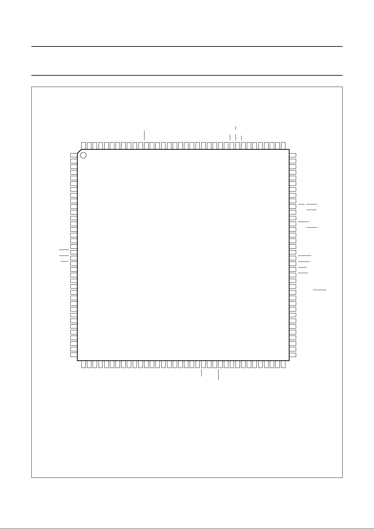
6 PINNING
SYMBOL PIN TYPE
DRIVE/
THRESHOLD
GROUPING DESCRIPTION
n.c. 1 −− −not connected
n.c. 2 −− −not connected
XDA0 3 O M RAM output address lines
XDA1 4 O M
XDA2 5 O M
V
DDD(pad6)
6 −− −digital peripheral supply voltage 6
DGND1 7 −− −digital ground 1
XDA3 8 O M RAM output address lines
XDA4 9 O M
XDA5 10 O M
XDA6 11 O M
XDA7 12 O M
XDA8 13 O M
XDA9 14 O M
XDA10 15 O M
XDA11 16 O M
DGND2 17 −− −digital ground 2
XRAS 18 O H RAM row address strobe output (active LOW)
XCAS 19 O H column address strobe output (active LOW)
XWR 20 O H write enable output (active LOW)
XDD0 21 I/O M/T RAM data bus input/output
XDD1 22 I/O M/T
V
DDD(core1)
23 −− −digital core supply voltage 1
DGND3 24 −− −digital ground 3
XDD2 25 I/O M/T RAM data bus input/output
XDD3 26 I/O M/T
XDD4 27 I/O M/T
XDD5 28 I/O M/T
XDD6 29 I/O M/T
XDD7 30 I/O M/T
V
DDD(pad7)
31 −− −digital peripheral supply voltage 7
DGND4 32 −− −digital ground 4
2
SCKI1 33 I C I
WSI1 34 I C I
S-bus I/O I2S-bus bit clock input
2
S-bus word select strobe input
1997 Aug 12 6
Page 7
Philips Semiconductors Objective specification
ATAPI CD-R block decoder SAA7381
SYMBOL PIN TYPE
DRIVE/
THRESHOLD
GROUPING DESCRIPTION
n.c. 35 to 38 −− −not connected
SDI1 39 I C I
2
S-bus I/O data input from CD engine
n.c. 40 O M not connected
SFSY 41 I/O L/C subcode I/O 3-wire subcode sync input/output
RCK 42 I/O L/C 3-wire subcode clock input/output
SUBI 43 I C Q and R-W subcode input
n.c. 44 O L not connected
CFLG 45 I C I
2
S-bus input CD error corrector flags and absolute time
sync
C2P0 46 I C CD C2 error correction flag input for ERCO
DGND5 47 −− −digital ground 5
IECO 48 O M multimedia IEC 958 output
MCK 49 I/O M/C multimedia
output
or 384fs clock for multimedia master
256f
s
clock/IEC 958 clock or divided system clock for
CD-DSP
SCK2 50 I/O L/C multimedia I
WS2 51 I/O L/C I
SDO2 52 O M I
2
S-bus bit clock input/output
2
S-bus word select strobe input/output
2
S-bus data output to DAC/video decoder
GND 53 −− −ground
CROUT 54 O crystal pad crystal oscillator crystal oscillator output
CRIN 55 I crystal pad crystal oscillator/clock input
V
I
DDA
ref
56 −− −analog supply voltage
57 analog current input clock generator VCO reference current
POR 58 I Schmitt trigger system power-on reset (active LOW)
TEST1 59 I C test mode control input test pins
TEST2 60 I C
RESET 61 I Schmitt trigger host ATAPI bus reset input from host (active LOW)
DD7 62 I/O AL/T host data bus input/output
DD8 63 I/O AL/T
DD6 64 I/O AL/T
V
DDD(pad1)
65 −− −digital peripheral supply voltage 1
DGND6 66 −− −digital ground 6
DD9 67 I/O AL/T host data bus pin order of ATAPI interface matches
DD5 68 I/O AL/T
DD10 69 I/O AL/T
the pinning of the 40-way IDE connector (slew
rate limiting by control of drive capability into
capacitive load of ATA bus)
DD4 70 I/O AL/T
1997 Aug 12 7
Page 8
Philips Semiconductors Objective specification
ATAPI CD-R block decoder SAA7381
SYMBOL PIN TYPE
DRIVE/
THRESHOLD
GROUPING DESCRIPTION
n.c. 71 to 74 −− −not connected
DD1 1 75 I/O AL/T host data bus; pin order of ATAPI interface matches
DD3 76 I/O AL/T
DD12 77 I/O AL/T
the pinning of the 40-way IDE connector (slew
rate limiting by control of drive capability into
capacitive load of ATA bus)
DD2 78 I/O AL/T
DD13 79 I/O AL/T
DD1 80 I/O AL/T
DD14 81 I/O AL/T
DD0 82 I/O AL/T
DD15 83 I/O AL/T
DMARQ/
DMACK
84 O AL host DMA request/SCSI DMA acknowledge output
(active LOW)
DGND7 85 −− −digital ground 7
V
DDD(pad2)
86 −− −digital peripheral supply voltage 2
DIOW 87 I L/T host write cycle write enable/control register write
input (active LOW)
DIOR 88 I L/T host read cycle read enable/control register read
input (active LOW)
IORDY 89 O AH host device is ready to transfer data output
(active LOW)
DMACK/
DMARQ
90 I T host DMA acknowledge (active LOW)/SCSI DMA
request input
INTRQ 91 A host host interrupt request (NB 3-state output)
DGND8 92 −− −digital ground 8
V
DDD(pad3)
93 −− −digital peripheral supply voltage 3
IOCS16 94 O AH host I/O port is 16-bit output (active LOW)
DA1/
DBWR 95 I/O L/T host address wire 1/DMA from generic interface is
output from the SAA7381 (active LOW)
PDIAG 96 I/O AL/T host ATAPI passed diagnostics input/output
(active LOW)
DA0 97 I/O L/T host address wire 0 input/output
DA2/
DBRD 98 I/O L/T host address wire 2/DMA from generic interface is
input to the SAA7381 (active LOW)
CS0/
SCSICS
99 I/O L/T host chip select 1FX/generic interface chip select
(active LOW)
CS1 100 I/O L/T host chip select 3FX input/output (active LOW)
DASP 101 I/O AH/T host device active slave present input/output (active
LOW)
INT2 102 O L sub-CPU sub-CPU interrupt output from the SAA7381
drive block and UART
1997 Aug 12 8
Page 9
Philips Semiconductors Objective specification
ATAPI CD-R block decoder SAA7381
SYMBOL PIN TYPE
DRIVE/
THRESHOLD
GROUPING DESCRIPTION
DGND9 103 −− −digital ground 9
V
DDD(pad4)
104 −− −digital peripheral supply voltage 4
COMACK 105 I C UART command acknowledge/transmit flow control
input
COMCLK 106 O L UART serial data clock for synchronous mode output
n.c. 107 to 110 −− −not connected
COMOUT 111 O L UART transmit data output
COMIN 112 I C UART receive data input
COMSYNC 113 I C UART basic engine synchronization input
SYSSYNC 114 I C UART basic engine synchronization input
SCCLK 115 O M sub-CPU sub-CPU clock output
RD 116 I T sub-CPU sub-CPU read enable (active LOW)
WR/R/W 117 I T sub-CPU sub-CPU write enable/and read/write control
input (active LOW)
INT 118 O L sub-CPU sub-CPU interrupt request output from host
interface (active LOW)
SRST 119 O L sub-CPU sub-CPU reset output
SCA0/SCD0 120 I/O L/T sub-CPU multiplexed address/data lines
SCA1/SCD1 121 I/O L/T
DGND10 122 −− −digital ground 10
V
DDD(pad5)
123 −− −digital peripheral supply voltage 6
SCA2/SCD2 124 I/O L/T sub-CPU multiplexed address/data lines
SCA3/SCD3 125 I/O L/T
SCA4/SCD4 126 I/O L/T
SCA5/SCD5 127 I/O L/T
SCA6/SCD6 128 I/O L/T
SCA7/SCD7 129 I/O L/T
DGND11 130 −− −digital ground 11
V
DDD(core2)
131 −− −digital core supply voltage 2
ALE 132 I T sub-CPU demultiplex enable input for lower address
lines
PSEN 133 I T sub-CPU program store enable (active LOW)
SCA15 134 I T sub-CPU upper address lines input
SCA14 135 I T
SCA13 136 I T
SCA12 137 I T
DGND12 138 −− −digital ground 12
1997 Aug 12 9
Page 10
Philips Semiconductors Objective specification
ATAPI CD-R block decoder SAA7381
SYMBOL PIN TYPE
SCA11 139 I T sub-CPU upper address lines input
SCA10 140 I T
SCA9 141 I T
SCA8 142 I T
n.c. 143 −− −not connected
n.c. 144 −− −not connected
DRIVE/
THRESHOLD
GROUPING DESCRIPTION
1997 Aug 12 10
Page 11
Philips Semiconductors Objective specification
ATAPI CD-R block decoder SAA7381
handbook, full pagewidth
V
DDD(pad6)
DGND1
XDA10
XDA11
DGND2
XRAS
XCAS
V
DDD(core1)
DGND3
V
DDD(pad7)
DGND4
SCKI1
n.c.
n.c.
XDA0
XDA1
XDA2
XDA3
XDA4
XDA5
XDA6
XDA7
XDA8
XDA9
XWR
XDD0
XDD1
XDD2
XDD3
XDD4
XDD5
XDD6
XDD7
WSI1
n.c.
n.c.
n.c.
n.c.
SCA8
SCA9
SCA10
SCA11
DGND12
SCA12
SCA13
SCA14
144
143
142
141
140
139
138
137
136
135
1
2
3
4
5
6
7
8
9
10
11
12
13
14
15
16
17
18
19
20
21
22
23
24
25
26
27
28
29
30
31
32
33
34
35
36
3738394041424344454647484950515253545556575859606162636465666768697071
n.c.
n.c.
SDI1
n.c.
SFSY
RCK
SUBI
n.c.
CFLG
C2P0
SCA15
PSEN
134
133
IECO
DGND5
DDD(core2)
ALE
V
132
131
MCK
SCK2
DGND11
SCA7/SCD7
130
129
SAA7381
WS2
SDO2
SCA6/SCD6
SCA5/SCD5
128
127
GND
CROUT
SCA4/SCD4
SCA3/SCD3
SCA2/SCD2
126
125
124
ref
I
DDA
CRIN
V
DDD(pad5)
V
DGND10
SCA1/SCD1
123
122
121
POR
TEST1
TEST2
SCA0/SCD0
SRST
INT
120
119
118
DD7
DD8
RESET
WR/R/WRDSCCLK
117
116
115
DD6
DGND6
DDD(pad1)
V
SYSSYNC
COMSYNC
COMIN
114
113
112
DD9
DD5
DD10
COMOUT
n.c.
n.c.
111
110
109
72
n.c.
n.c.
DD4
n.c.
108
n.c.
107
COMCLK
106
105
COMACK
V
104
DDD(pad4)
DGND9
103
INT2
102
DASP
101
CS1
100
CS0/SCICS
99
DA2/DBRD
98
DA0
97
96
PDIAG
95
DA1/DBWR
IOCS16
94
V
93
DDD(pad3)
DGND8
92
INTRQ
91
90
DMACK/DMARQ
89
IORDY
88
DIOR
87
DIOW
V
86
DDD(pad2)
DGND7
85
84
DMARQ/DMACK
DD15
83
DD0
82
DD14
81
DD1
80
DD13
79
DD2
78
DD12
77
DD3
76
DD11
75
n.c
74
n.c.
73
MGL180
Fig.2 Pin configuration.
1997 Aug 12 11
Page 12
Philips Semiconductors Objective specification
ATAPI CD-R block decoder SAA7381
6.1 Detailed description of pin functions Table 1 Q and R-W input/output subcode connections (4 pins)
SYMBOL DESCRIPTION COMMENT
SFSY 3-wire subcode sync input subcode frame sync for receiving 3-wire subcode; output
subcode frame sync for transmitting 3-wire subcode
RCK 3-wire subcode clock output bit clock for receiving 3-wire subcode; input bit clock for
transmitting 3-wire subcode
SUBI Q and R-W subcode input configurable for 3-wire or Philips V4 subcode mode; can use either
RCK or WSI1 as clock references with appropriate dividers
2
Table 2 I
SYMBOL DESCRIPTION COMMENT
MCK 256f
SCK2 I
WS2 I
SDO2 I
IECO IEC 958 output the IEC 958 output combines multimedia data and Q-W subcode
S-bus multimedia audio output (5 pins)
or 384fs clock for
s
multimedia master
clock/IEC 958 clock or
divided system clock for
Clock reference input pin when interface is in a master mode; a
programmable divider is provided. This pin is also configurable as a
programmable clock output intended as a clock reference for a
CD-DSP. Should be pulled up if not in use.
CD-DSP
2
S-bus bit clock This is used for master and slave I2S-bus application as both modes
are needed. For instance, the Philips multimedia CODEC is an I2S-bus
slave, hence this must be a master interface. When driving some
DACs, this interface can be a slave.
2
S-bus left/right strobe word select strobe either master or slave
2
S-bus data to DAC/video
I2S-bus multimedia data
decoder
2
Table 3 I
S-bus connections to CD engine (6 pins)
SYMBOL DESCRIPTION COMMENT
SCKI1 I
2
S-bus bit clock this is a separate clock to the multimedia bit clock as this rate is
derived from the disc linear velocity
2
WSI1 I
SDI1 I
C2P0 CD C2 error corrector flag
CFLG CD error corrector flags and
S-bus left/right strobe
2
S-bus data from CD-DSP
from ERCO
absolute time sync
these flags are used to indicate errors from second layer correction to
the ERCO
The absolute time sync is used in the CD input process for playing
‘Red Book’ discs; the error corrector status is also read in from this
signal, to provide an indication of C1 and C2 performance for CD-RW
applications.
1997 Aug 12 12
Page 13
Philips Semiconductors Objective specification
ATAPI CD-R block decoder SAA7381
Table 4 ATAPI target mode interface
ATAPI
NAME
RESET ATAPI reset signal: the SAA7381 will not recognize a signal assertion shorter than 20 ns as a valid
reset signal.
DD0 to DD7 ATAPI D0 to D7.
DD8 to DD15 ATAPI D8 to D15: these data bits are only used in accesses to the 16-bit data port.
DMARQ DMA request: this signal, used for DMA data transfers between host and device, is asserted by the
SAA7381 when it is ready to transfer data to or from the host. The direction of data transfer is
controlled by
DMACK DMA acknowledge: this signal is used by the host in response to DMARQ to initiate DMA transfers.
This signal may be temporarily negated by the host to suspend the DMA transfer in process.
IOCS16 ATAPI I/O port is a 16-bit open-drain output: during PIO transfer Modes 0, 1 or 2, IOCS16 indicates to
the host system that the 16-bit data port has been addressed and that the device is prepared to send
or receive a 16-bit data word.
IORDY ATAPI I/O ready open-drain output: this signal is negated to extend the host transfer cycle of any host
register access (read or write) when the SAA7381 is not ready to respond to a data transfer request.
This signal is only enabled during DIOR/DIOW cycles to the SAA7381. When IORDY is not active, it is
in the high-impedance (undriven) state.
DA0 to DA2 Address bus (device address).
DIOW ATAPI write strobe: the rising edge of DIOW latches data from the signals, DD0 to DD7 or
DD0 to DD15 into a register or the data port of the SAA7381. The SAA7381 will not act on the data
until it is latched.
DIOR ATAPI read strobe: the falling edge ofDIOR enables data from a register or data port ofthe SAA7381
onto the signals, DD0 to DD7 or DD0 to DD15. The rising edge of DIOR latches data at the host and
the host will not act on the data until it is latched.
CS0 ATAPI chip select 0 input: this is the chip select signal from the host used to select the ATA command
block registers. This signal is also known as CS1FX.
CS1 ATAPI chip select 1 input: this is the chip select signal from the host used to select the ATA control
block registers. This signal is also known as CS3FX.
INTRQ ATAPI interrupt output: this signal is used to interrupt the host system. INTRQ is asserted only when
the device has a pending interrupt, the device is selected, and the host has cleared the ‘nien’ bit in the
device control register. If the ‘nien’ bit is equal to 1, or the device is not selected, this output is in a
high-impedance state, regardless of the presence or absence of a pending interrupt.
PDIAG ATAPI passed diagnostics: this signal shall be asserted by device 1 to indicate to device 0 that it has
completed diagnostics.
DASP ATAPI DASP (device active, device 1 present): this is a time-multiplexed signal which indicates that a
device is active, or that device 1 is present. This signal is an open-drain output.
DIOR and DIOW.
ATAPI MEANING
1997 Aug 12 13
Page 14
Philips Semiconductors Objective specification
ATAPI CD-R block decoder SAA7381
Table 5 Generic host controller interface
ATAPI
NAME
RESET RESET controller reset output
DD0 to DD7 D0 to D7 controller DMA path/controller data and control bus (optional)
DD8 to DD15 D8 to D15 controller upper DMA path (optional)
DMARQ
DMACK DMARQ DMA request from controller
DA1
DA2
CS0 SCSICS controller chip select output for sub-CPU read/write cycles
Table 6 Miscellaneous pins
SYMBOL DESCRIPTION COMMENT
CRIN crystal oscillator/clock input −
CROUT crystal oscillator output −
I
ref
POR power-on reset pin −
TEST1 and TEST2 mode control test pins −
Table 7 Sub-CPU interface pins
GENERIC
INTERFACE
NAME
DMACK DMA acknowledge to controller
DBWR DMA bus write to controller
DBRD DMA bus read from controller
VCO reference current clock PLL multiplier
GENERIC HOST CONTROLLER INTERFACE MEANING
SYMBOL DESCRIPTION COMMENT
SRST sub-CPU reset active HIGH reset if XDD7 is pulled LOW during power-on reset;
active LOW reset if XDD7 is pulled HIGH during power-on reset
INT sub-CPU interrupt request
output from host interface
INT2 sub-CPU interrupt output
from the SAA7381 drive
block and UART
SCCLK sub-CPU clock out −
RD sub-CPU read enable sub-CPU read enable strobe; if grounded permanently, the WR
WR/R/W sub-CPU write enable/
read/write control
ALE demultiplex enable input for
lower address lines
PSEN program store enable this pin should be tied high using a 10 kΩ resistor
SCD0 to SCD7/
SCA0 to SCA7
SCA8 to SCA15 sub-CPU address high bits −
sub-CPU data bus
multiplexed/low address bus
open-drain sub-processor interrupt from host interface
open-drain sub-processor interrupt from drive and UART
signal will act as read/write control input
write enable; alternative usage is read/write if RD is held LOW at all
times; WR has priority over RD at all times
while HIGH, the lower address bits are latched from
SCD0 to SCD7; should be used with a Schmitt trigger input to
avoid false latching due to ground bounce on the
8051 microcontroller
−
1997 Aug 12 14
Page 15

Philips Semiconductors Objective specification
ATAPI CD-R block decoder SAA7381
Table 8 RAM interface pins
SYMBOL DESCRIPTION COMMENT
XDA0 to XDA11 RAM address bits, multiplexed for DRAM up to 16 Mbytes DRAM only supported
XRAS DRAM row address strobe
XCAS DRAM column address strobe
XWR RAM write enable
XDD0 to XDD7 RAM data bus
Table 9 Basic engine interface
SYMBOL DESCRIPTION COMMENT
SYSSYNC basic engine synchronization input generate interrupts on rising and/or falling edges
COMSYNC basic engine synchronization input generate interrupts on rising and/or falling edges
COMIN receive data −
COMOUT transmit data −
COMCLK serial data clock for synchronous mode −
COMACK command acknowledge/transmit flow
control
must be HIGH for synchronous mode to transmit next
data byte
7 FUNCTIONAL DESCRIPTION
The SAA7381 device consists of a number of main
functional units; a CD engine interface, a multimedia block,
a microcontroller interface, an error detection and
correction block, a host interface and a memory manager.
There are also several smaller blocks including a clock
control block and a UART for communication with the CD
engine. Each block is independently controlled by a
dedicated register set. These registers are memory
mapped to the sub-CPU to allow for faster access.
The external RAM can also be accessed directly from the
microcontroller to support scratchpad accesses and thus
eliminate the need for further memory devices in the
system.
7.1 Memory field description
The CD input function of the SAA7381 buffer manager
receives the main data stream in I
CD-DSP, performs sync detection and partitions the data
into blocks.
2
S-bus format from the
It then writes the blocks to the buffer memory and onboard
ERCO RAM. Any detected errors are then corrected and
over written into the buffer memory.
Memory is segmented and addressable by segment
pointers. The segment pointers consist of a block number,
offset pointer and byte number within the block. The data
within each segment is organised in the same manner
(see Table 10).
The arrangement of data within each segment in memory
differs from other Philips devices, because of the different
error correction processing possibilities within the
SAA7381.
Addresses 0 to 2355 are written to memory by the drive
processor when enabled.
1997 Aug 12 15
Page 16

Philips Semiconductors Objective specification
ATAPI CD-R block decoder SAA7381
Table 10 The memory map of a block in the buffer RAM for standard density mode (see Table 11)
ADDRESS (OFFSET) TYPE OF DATA
0 to 3 header field
4 to 2339 block data field
2340 to 2351 sync field
2352 copy of STAT0
2353 copy of STAT1
2354 copy of STAT2
2355 number of C2 flags in sector (compressed format)
2356 to 2451 96-byte de-interleaved R-W data field
2452 to 2463 12-byte Q-subcode field
2464 to 2465 copy of STAT4 field; only valid if ERCO did run on this block
2466 to 2559 user work space
Table 11 Description of Table 10
DATA DESCRIPTION
Header field The 4-byte header data consists of a 3-byte block address of absolute time (minutes,
seconds and frame, bytes 0 to 3). The fourth byte is for the mode of data:
Mode 0 = zero mode
Mode 1 = data storage with EDC and ECC
Mode 2 = data storage
Block data field in the CD-ROM mode the block data consists of 2048 bytes of user data and 288 bytes of
auxiliary data
User data:
Mode 0= all 2048 bytes in user data are zero
Mode 1= all 2048 bytes are available to the user
Mode 2= all 2048 bytes are available to the user
Auxiliary data:
Mode 0= all 288 bytes in Aux data are zero
Mode 1= the Aux field is in accordance with the EDC and ECC specification
Mode 2= all 288 bytes are available to the user
Sync field The 12-byte sync field is the next segment in memory. All bytes in the sync field are FFH,
except the first and last bytes which are $00.
1997 Aug 12 16
Page 17

Philips Semiconductors Objective specification
ATAPI CD-R block decoder SAA7381
DATA DESCRIPTION
Number of C2 flags in
sector (compressed
format)
96-byte de-interleaved
R-W data field
12-byte Q-subcode field As above: these will not be separated out if the copy2 interleaving option is set to raw.
2 copies of STAT4 field Address 2465 and 2466 are copies of the STAT4 register written by the ERCO when
While storage of C2 flag positions is not possible as a consequence of the architecture of
the SAA7381, a count of the number of flags seen per block is made in a single-byte
counter. This counter packs the possibly 12-bit count into a single byte in the following
way, at the expense of resolution in the count values for large counts.
C2count_val = count (5 down to 0) × [4 ^ count (7 down to 6)], the resolution of the count
is therefore:
C2count_val 0 to 63: counter resolution = 1
C2count_val 64 to 255: counter resolution = 4
C2count_val 256 to 1023: counter resolution = 16
C2count_val 1024 to 4095: counter resolution = 64
Written to memory by the automatic Q-channel copy process (copy2 channel). If the copy
process is not enabled, these fields are not written (see Section 7.3.5). These bytes may
either be R-W de-interleaved or presented as raw Q-W subcode bytes. If the copy2
interleaving mode is set to raw, interleaved copying is still required as the subcode
temporary holding buffer has Q bytes interspersed with the raw R-W.
enabled. This allows the user to determine if the ST AT4 register has been written to by the
ERCO. If seg2465 = seg2466 then STAT4 definitely has not been written by the ERCO.
If seg2465 ≠ seg2466 then STAT4 probably has not been written by the ERCO.
Via direct access to buffer memory, the sub-CPU will be able to look at all of the blocks so
far corrected, to check their status, in a background task.
ERCO failures do not have to be dealt with immediately, as the status of every block
loaded in to RAM is stored with that block, and it is not overwritten until the RAM block is
filled with new data from CD input.
The error corrector will be controlled additionally to permit the use of single pass P-Q or
only EDC operation to allow for greater than n = 14 operation of the ERCO.
The ERCO status will be copied into the RAM along with the data. This is possible
because the RAM now has spare capacity to store the information, as part of the change
from linear to segment/offset addressing.
It is possible to program transfers into RAM of more than one block without processor
intervention. It is also possible to continually loop on the same buffer area of RAM, by not
altering the reload register values when the reload interrupt occurs.
7.1.1 DVD-ROM MEMORY FIELD INFORMATION The buffer arrangement for DVD usage is basically the same (data followed by flags) but the size of the block data differs,
and the ERCO flags are at a different offset, and as the ERCO is not in use, the flags relating to ERCO performance will
not be valid.
1997 Aug 12 17
Page 18
Philips Semiconductors Objective specification
ATAPI CD-R block decoder SAA7381
7.2 CD input control registers
The CD input process is intended to be as automated as possible. Data is read in from the front end, descrambled if in
CD-ROM mode and then written to RAM. The registers that control the address of where the data is written to are in the
memory processor block.
The input data is synchronized, decoded and written to the buffer RAM. The input data format is software programmable.
The synchronization is performed by using a sync detector and a sync interpolator. The sync detector can detect
CD-ROM syncs and syncs from the CFLG pin, for use with Red Book, audio and for DVD. When no sync is found, it is
optionally interpolated.
After decoding, each full sector of data (2352 bytes) comprising sync, header and sub-header is written to the buffer
RAM. The R-W and Q subcode is added by a software-initiated automatic block copy process.
7.2.1 R
Table 12 IFCONFIG (write only; address FF10H) (see Table 13)
Table 13 Description of the IFCONFIG register bits
EGISTERS ASSOCIATED WITH DATA IN PROCESS
BIT 7 BIT 6 BIT 5 BIT 4 BIT 3 BIT 2 BIT 1 BIT 0
ipconfig ckdiv1 ckdiv0 subsel modulo 1 modulo 0 config swap config wclk
BIT NAME VALUE MEANING
7 ipconfig 0 I
1 EIAJ serial interface mode
6 and 5 ckdiv1 and
ckdiv0
4 subsel 0 both copies of sub-header contribute to STAT1/sh0err to sh3err
3 and 2 modulo 1 and
modulo 0
1 config swap 0 the received data from the CD-DSP or drive FIFO is not swapped
0 config wclk 0 the internal ‘irclk’ is not inverted
00 oversample, bit clock division ratio = 2
01 oversample, bit clock division ratio = 4
10 oversample, bit clock division ratio = 8
11 bit clock division ratio = 1 (no division)
1 first copy only of sub-header contributes to STAT1/sh0err to sh3err
00 modulo count 2352
01
10 modulo count 2064
11 modulo count 2064, but do not count bytes with flag = 1
1 the received data from the CD-DSP or drive FIFO is swapped
1 the internal ‘irclk’ is inverted
2
S-bus mode
1997 Aug 12 18
Page 19
Philips Semiconductors Objective specification
ATAPI CD-R block decoder SAA7381
Table 14 CD input control registers (see Table 15)
ADDRESS NAME BIT 7 BIT 6 BIT 5 BIT 4 BIT 3 BIT 2 BIT 1 BIT 0
FF21H DRIVECURSEG-L s7 s6 s5 s4 s3 s2 s1 s0
FF20H DRIVECURSEG-H incen wren − s12 s11 s10 s9 s8
FF60H DRIVECURCOUNT c7 c6 c5 c4 c3 c2 c1 c0
FF27H DRIVENEXTSEG-L s7 s6 s5 s4 s3 s2 s1 s0
FF26H DRIVENEXTSEG-H incen wren − s12 s11 s10 s9 s8
FF61H DRIVENEXTCOUNT c7 c6 c5 c4 c3 c2 c1 c0
FF23H DRIVEPREVSEG-L s7 s6 s5 s4 s3 s2 s1 s0
FF22H DRIVEPREVSEG-H incen wren − s12 s11 s10 s9 s8
FF24H DRIVEOFFSET-H s7 s6 s5 s4 s3 s2 s1 s0
FF25H DRIVEOFFSET-L s7 s6 s5 s4 s3 s2 s1 s0
There are two sets of address registers, one giving the current (DRIVECURSEG) number of the segment being filled and
a segment/block counter. The other set contains the values (DRIVENEXTSEG) to use on completion of the current group
of blocks being filled or emptied (in CD-R). The DRIVEPREVSEG register is loaded with the value of the DRIVECURSEG
register at the end of each CD-ROM block.
The reloading of the registers will trigger an interrupt, if enabled, of the sub-CPU, which will then have to reload the ‘next’
registers. before the transfer requested in the ‘current’ registers are exhausted.
Memory is split into segments, each segment is 2560 bytes. The drive data is written one block at a time at the segment
number pointed to by the DRIVECURSEG register. For the next block the ‘DRIVECURSEG’ is updated as follows.
Table 15 Description of the ‘incen’ and ‘wren’ bits (see Table 14)
BIT NAME VALUE MEANING
(2)
(1)
0 hold value of DRIVECURSEG
1 increment DRIVECURSEG at the end of each CD-ROM block received
0 enable writes of data transferred
1 disable write of data transferred
7 incen
6 wren
Notes
1. If ‘incen’ is logic 1, the ‘DRIVECURSEG’ pointer will increment every sector sync. The ‘DRIVECURCOUNT’ will
decrement every sector sync independent of ‘incen’. If ‘incen’ is logic 0 then the pointer will remain fixed pointing at
the same segment of RAM. If the reading of data from CD is enabled by the ‘wrreq’ bit in the CTRL0 register, and
the ‘wren’ bit is logic 0 the segment will be repeatedly filled by the data coming in from the CD-ROM.
2. If ‘wren’ is logic 1 and ‘incen’ is logic 1 then the DRIVECURSEG register will increment with each sync time and the
DRIVECURCOUNT register will decrement but data will not be written to external RAM. This allows the triggering of
the reading of data or the writing of data some time in the future.
Table 16 Control and status registers (see Tables 17, 18 and 19)
ADDRESS NAME BIT 7 BIT 6 BIT 5 BIT 4 BIT 3 BIT 2 BIT 1 BIT 0
FF0DH CTRL0 decen ahead e01rq autoform eramrq wrreq eccrq encode
FF0EH CTRL1 syien syden asyn cowren onepass − − −
FF0FH CTRL2 modrq formrq − automode mbckrq − dscren −
1997 Aug 12 19
Page 20

Philips Semiconductors Objective specification
ATAPI CD-R block decoder SAA7381
Table 17 Description of the CTRL0 register bits (resetting the chip sets all the bits in this register to 0)
BIT NAME VALUE DESCRIPTION
2
7 decen 0 disable decoding, drive in ‘full reset’ state, no monitor of I
interrupts
1 enable decoding
6 ahead 0 obsolete
1 must be set to logic 1
5 e01rq 0 disable error correction of bytes for which an error has been detected, but not
yet corrected
1 enable CRC miscorrection correction of the C2 flag bytes
4 autoform 0 disable automatic Form detection
1 enable automatic Form detection
3 eramrq 0 disable erasure flag use
1 enable erasure flag use
2 wrreq 0 disable data writes to the buffer and pointer updates, only header and status
information recovered
1 enables data writes to the buffer and pointer updates
1 eccrq 0 disable ECC correction only EDC checking
1 enable ECC correction, ERCO active
0 encode 0 must be set to logic 0
1
S-bus line, no
Table 18 Description of the CTRL1 register bits (the reset function clears all the flags in this register)
BIT NAME VALUE DESCRIPTION
7 syien 0 disable sync interpolation
1 enable sync interpolation
6 syden 0 disable sync detection
1 enable sync detection
5 asyn 0 CD-ROM sync detection
1 audio sync detection
4 cowren 0 disable rewriting of corrected error bytes
1 enable rewriting of error bytes during error correction
3 onepass 0 normal error corrector operation
1 one pass only error correction
1997 Aug 12 20
Page 21
Philips Semiconductors Objective specification
ATAPI CD-R block decoder SAA7381
Table 19 Description of the CTRL2 register bits
BIT NAME VALUE DESCRIPTION
7 modrq 0 Mode 1 request
1 Mode 2 request
6 formrq 0 Form 1 request
1 Form 2 request
4 automode 0 disable automatic determination of mode bit
1 enable automatic determination of mode bit
3 mbckrq 0 disable mode check function
1 enable mode check function
1 dscren 0 disable descrambling function
1 enable descrambling function
Table 20 Sub-CPU registers during read (see Tables 21, 22, 23, 27 and 28)
ADDRESS NAME BIT 7 BIT 6 BIT 5 BIT 4 BIT 3 BIT 2 BIT 1 BIT 0
FF00H HEAD0 minutes
FF01H HEAD1 seconds
FF02H HEAD2 frames
FF03H HEAD3 mode
FF04H SUBHEAD0 file number
FF05H SUBHEAD1 channel number
FF06H SUBHEAD2 submode
FF07H SUBHEAD3 coding Information
FF08H STAT0 − ilsync nosyn lblk − sblk erablk −
FF09H STAT1 minerr secerr blkerr moderr sh0err sh1err sh2err sh3err
FF0AH STAT2 rmod3 rmod2 rmod1 rmod0 mode form rform1 rform2
FF0BH STAT3 valst − − − − − − −
FF0CH STAT4 crcok cblk uceblk − nocor mode form qok
Table 21 Description of the STAT0 register bits (resetting the chip clears all bits in this register)
BIT NAME VALUE DESCRIPTION
7 −−reserved
− reserved
6 ilsync 0 −
1 sync pattern detected at word count 0 to 1174
5 nosyn 0 −
1 sync pattern inserted by sync interpolator not coincident with data sync
4 lblk 0 −
1 with ‘syien’ at logic 0, no sync found; data block size has been extended
3 −−reserved
− reserved
1997 Aug 12 21
Page 22
Philips Semiconductors Objective specification
ATAPI CD-R block decoder SAA7381
BIT NAME VALUE DESCRIPTION
2 sblk 0 −
1 short block indication
1 erablk 0 −
1 one or more bytes of the block are flagged with C2 flags
0 −−reserved
− reserved
Table 22 Description of the STAT1 register bits; address FF09H (see notes 1 and 2)
BIT 7 BIT 6 BIT 5 BIT 4 BIT 3 BIT 2 BIT 1 BIT 0
(3)
minerr
Notes
1. Resetting the chip clears all bits in this register.
2. The bits in this register indicate the reliability of data in the HEAD0 to HEAD3 and SUBHEAD0 to SUBHEAD3
registers.
3. Bits ‘minerr’, ‘secerr’, ‘blkerr’ and ‘moderr’ indicate errors in the minutes, seconds, frames and mode bytes in the
header of the current block.
4. Bits ‘sh0err’ to ‘sh3err’ indicate errors in the respective bytes in the subheader.
secerr
(3)
blkerr
(3)
moderr
(3)
sh0err
(4)
sh1err
(4)
sh2err
(4)
sh3err
(4)
Table 23 Description of the STAT2 register bits; address FF0AH (see Tables 24, 25 and 26)
BIT 7 BIT 6 BIT 5 BIT 4 BIT 3 BIT 2 BIT 1 BIT 0
rmod3 rmod2 rmod1 rmod0 mode form rform1 rform2
Table 24 Description of the ‘mode’ and ‘form’ bits
mode form SETTING
0 0 Mode 1
1 0 Mode 2, Form 1
X 1 Mode 2, Form 2 or ECC correction impossible
Table 25 Description of the ‘rform’ bits
rform1 rform2 MEANING
0 0 Form 1
0 1 Form 2
1 X error in Form byte
1997 Aug 12 22
Page 23
Philips Semiconductors Objective specification
ATAPI CD-R block decoder SAA7381
Table 26 Description of the ‘rmod’ bits
rmod3 to rmod30
0000 mode 0
0001 mode 1
0010 mode 2
0011 mode 3
0100 mode 4
0101 mode 5
0110 mode 6
0111 mode 7
1XXX packet written CD-R, run in/run out, link, XXX is mode
1111 mode = 7 or error in mode byte
Note
1. rmod3 = bit 7 #, bit 6 #, bit 5 #, bit 4 #, bit 3 # C2P0 (where # is logic OR). This is non-zero for packet written CD-R.
rmod2 = bit 2 # C2P0 (where C2P0 is C2 flag for mode byte).
rmod1 = bit 1 # C2P0 (where C2P0 is C2 flag for mode byte).
rmod0 = bit 0 # C2P0 (where C2P0 is C2 flag for mode byte).
(1)
MEANING
Table 27 Description of the STAT3 register bit
BIT NAME VALUE DESCRIPTION
7 valst 0 registers associated with decoder interrupt valid
1 registers invalid
Table 28 Description of the STAT4 register bits (this register contains the interrupt status on reading)
BIT NAME VALUE DESCRIPTION
7 crcok 0 −
1 cyclic redundancy check OK
6 cblk 0 −
1 there has been an error in this block
5 uceblk 0 −
1 uncorrectable errors in block
4 − 0 reserved
1 reserved
3 nocor 0 −
1 ERCO was not started on this block
2 mode 0 Mode 1 used in correcting this block
1 Mode 2 used in correcting this block
1 form 0 Form 1 used in correcting this block
1 Form 2 used in correcting this block
0 qok 0 Q channel CRC no error
1 Q channel CRC error
1997 Aug 12 23
Page 24

Philips Semiconductors Objective specification
ATAPI CD-R block decoder SAA7381
Table 29 Auxiliary segment pointer
ADDRESS NAME BIT 7 BIT 6 BIT 5 BIT 4 BIT 3 BIT 2 BIT 1 BIT 0
FF29H AUXSEGMENT-L s7 s6 s5 s4 s3 s2 s1 s0
FF28H AUXSEGMENT-H − − − s12 s11 s10 s9 s8
The auxiliary segment pointer points at a group of
segments which hold the data FIFOs used in the
SAA7381. These are the ‘large’ FIFOs rather than the
small resynchronizing FIFOs inside the SAA7381.
The subcode input/output and n = 1 I2S-bus interfaces use
these FIFOs (in addition, the shadow debug registers can
use some of this space).
The FIFOs are arranged to optimally occupy a contiguous
group of segments in the external RAM.
7.3 Multimedia output interface
This block deals with subcode input and output in addition
to an audio output which is independent of the I
2
S-bus
input output path connected to the CD-R engine.
Q and R-W subcode features:
• Supports semiautomatic de-interleaving/interleaving
• Subcode sync is aligned with the start of the current
block in RAM
• Supports subcode resynchronization when subcode
sync is lost
• Supports Philips ‘V4’ and 3-wire formats
• Has selectable polarity on RCK
• Uses WSI1 pin as timing reference
• Supports regeneration of subcode from IEC 958 output
using WS2 as timing reference
• Can accept subcode input while I2S-bus from CD-DSP
is oversampled audio at n = 2 or n = 4 oversample
Audio output (multimedia) features:
• Has data output for simple audio or digital video for
n = 1 or n = 2 rate regardless of input CD-DSP data rate
• 4096-byte FIFO for audio samples, requires firmware
polling for refills using the block copy engine
• Permits CAV and quasi-CLV systems to maintain n = 1
audio output
• Basic channel swap, mono-L or mono-R modes,
includes muting and L + R summed mono
• IEC 958 output with subcode Q-W for use in CAV and
other modes where there is no n = 1 clock in the
CD-DSP subsystem
– IEC 958 interface has fully programmable category
code and copyright bits for flexibility
– Subcode on IEC 958 is only available in CD-ROM
mode, because the subcode output FIFO is shared.
2
• Master and slave I
S-bus modes are available
– IEC 958 is only available when the I2S-bus is in the
master mode.
• Can be configured to provide a clock for an external
CD-DSP function via the MCK pin
• Can operate in 64fs or 48fs I2S-bus modes
• IEC 958 can operate at n = 2 although not permitted by
standard.
7.3.1 S
UBCODE INPUT BLOCK
7.3.1.1 Q-W subcode handling
The subcode data is initially converted from
serial-to-parallel format and is then handled as Q-W bytes.
The de-interleaving is performed by a de-interleaving
block copy mode in the memory processor’s block copy
engine. Subcode blocks will always be aligned with a block
of CD-ROM data, although the subcode Minutes,
Seconds, Frames (MSF) absolute time may have an
uncertainty of ±5 frames in terms of the actual CD-ROM
block it is referring to. This offset is unknown but consistent
in any given application. The block copy engine will be
automatically triggered when the subcode synchronization
is found.
The error corrector will then compute the CRC syndrome
of the subcode and deposit it in the CRC bytes.
The sub-CPU will have to perform the actual correction if a
non-zero syndrome appears.
This syndrome, if calculated during encoding by the
ERCO, can be used as the CRC written to disc for the
subcode.
1997 Aug 12 24
Page 25
Philips Semiconductors Objective specification
ATAPI CD-R block decoder SAA7381
7.3.1.2 Description of subcode interface
The subcode interface allows the reception and transmission of subcodes. The subcodes will be received/transmitted to
two on-chip 512-byte FIFOs, one for transmit and one for receive. No interrupts are associated with these FIFOs as the
block copy engine removes data or fills these as necessary.
There is, however, an interrupt which is asserted when a sync is found in an unexpected location.
7.3.2 S
Table 30 Subcode mode transmit control register (SUBMODETX; address FF13H); see Table 31
Table 31 Description of the SUBMODETX register bits
Note
1. Philips V4 subcode transmit mode must be selected for correct insertion of subcode into the IEC 958 data stream.
Table 32 Subcode mode receive control register (SUBMODERX, address FF17H); see Table 33
UBCODE MODE TRANSMIT CONTROL REGISTER
BIT 7 BIT 6 BIT 5 BIT 4 BIT 3 BIT 2 BIT 1 BIT 0
− − − pbit − txena − V4
BIT NAME VALUE DESCRIPTION
4 pbit 0 P bit logic 1 in 3-wire mode (default)
1 P bit logic 0 in 3-wire mode
2 txena 0 subcode transmit interface is disabled
1 subcode transmit interface is enabled
0 V4 0 Philips SRI 3-wire subcode
1 Philips V4 mode; note 1
BIT 7 BIT 6 BIT 5 BIT 4 BIT 3 BIT 2 BIT 1 BIT 0
− − − wsdiv1 wsdiv0 rxena rckinvrx rxsubqw
Table 33 Description of the SUBMODERX register bits
BIT NAME VALUE DESCRIPTION
4 wsdiv1 00 no oversampling (normal CD-ROM modes)
01 2 times oversampling
3 wsdiv0 10 4 times oversampling
11 8 times oversampling
2 rxena 0 subcode receive interface is disabled
1 subcode receive interface is enabled
1 rckinvrx 0 normal RCK output
1 invert the RCK output
0 rxsubqw 0 3-wire subcode
1 Philips V4 mode (sub Q-W)
1997 Aug 12 25
Page 26
Philips Semiconductors Objective specification
ATAPI CD-R block decoder SAA7381
Table 34 Subcode general (input/output pointers)
ADDRESS NAME BIT 7 BIT 6 BIT 5 BIT 4 BIT 3 BIT 2 BIT 1 BIT 0
FF2BH SUBPOINTR-L s7 s6 s5 s4 s3 s2 s1 s0
FF2AH SUBPOINTR-H − − − − − − − s8
FF2FH SUBPOINTW-L s7 s6 s5 s4 s3 s2 s1 s0
FF2EH SUBPOINTW-H − − − − − − − s8
FF2DH SUBBASEPOINTR-L s7 s6 s5 s4 s3 s2 s1 s0
FF2CH SUBBASEPOINTR-H − − − − − − − s8
FF31H SUBBASEPOINTW-L s7 s6 s5 s4 s3 s2 s1 s0
FF30H SUBBASEPOINTW-H − − − − − − − s8
7.3.2.1 Subcode buffering
The subcode is buffered in the AUXSEGMENT register. Two offset pointers, SUBPOINTR-L and SUBPOINTR-H, and
SUBPOINTW-L and SUBPOINTW-H are associated with it. The R pointer is for the subcode output and the W pointer
for the subcode input.
Pointers are also provided to point at the offset into the AUXSEGMENT register where the start of a subcode frame will
be found, SUBBASEPOINTR-L and SUBBASEPOINTR-H and SUBBASEPOINTW-L and SUBBASEPOINTW-H. The
block copy engine is expected to use these to automatically move the subcode into the segment pointed at by
DRIVECURSEG register.
7.3.3 G
ENERAL DESCRIPTION OF THE MULTIMEDIA OUTPUT INTERFACE
Table 35 Multimedia output interface register bits
ADDRESS NAME BIT 7 BIT 6 BIT 5 BIT 4 BIT 3 BIT 2 BIT 1 BIT 0
FF32H CDDA-H − − − − − − a9 a8
FF33H CDDA-L a7 a6 a5 a4 a3 a2 a1 a0
FF34H DAOFFSET-H − − − − a11 a10 a9 a8
FF35H DAOFFSET-L a7 a6 a5 a4 a3 a2 a1 a0
FF16H MMCTRL
FF70H IECCTRL
(1)
(2)
mmdiv spdx2 wslen mcksel
iecen data copyright preem vbit − accu
FF71H IECCAT cat7 cat6 cat5 cat4 cat3 cat2 cat1 cat0
FF14H MMAUD
FF15H MCK_CON
(3)
(4)
daen eiaj master − leftmode rightmode
− − − − mckxtal mckoe div
Notes
1. See Table 36.
2. See Table 39.
3. See Table 38.
4. See Table 41.
1997 Aug 12 26
Page 27

Philips Semiconductors Objective specification
ATAPI CD-R block decoder SAA7381
7.3.3.1 Basic description of the multimedia output interface
The multimedia data output may be used either with an internal clock or an externally provided clock. The clock used
should be a correct multiple of 44100 Hz in order for the block to correctly output IEC 958.
The multimedia interface data FIFO is located in the block of segments associated with AUXSEGMENT master/slave
mode operation (see Fig.3).
handbook, full pagewidth
e.g. DAC
SAA7381
SCK
WS
SDO2
slave: master = 0
e.g. DAC
SCK
WS
SDO2
master: master = 1
Fig.3 Master/slave mode operation.
Table 36 Description of the MMCTRL register bits
BIT NAME VALUE DESCRIPTION
7 mmdiv − see Table 37
6 −
5 −
4 −
3 spdx2 0 I
1I
2 wslen 0 I
1I
2
S-bus output is single speed
2
S-bus (and IEC 958) output is double speed; video applications
2
S-bus bit clock is 64 times the sample rate
2
S-bus bit clock is 48 times the sample rate
1 and 0 mcksel 00 multimedia internal clock is CRIN pin
01 multimedia internal clock is MCK pin
10 multimedia internal clock is system clock
SAA7381
MGL179
1997 Aug 12 27
Page 28
Philips Semiconductors Objective specification
ATAPI CD-R block decoder SAA7381
Table 37 mmdiv/mcksel relationship to clocks needed for I2S-bus and IEC 958
2
S-BUS OUTPUT
I
2
DIVIDER CODE
mmdiv
0000 48f
0001 64f
0010 96f
0011 128f
0100 192f
0101 256f
0110 384f
0111 512f
1000 768f
1001 1024f
1010 1536f
MULTIMEDIA
CLOCK
OVERSAMPLE
s
s
s
s
s
s
s
s
s
s
s
mcksel
S-BUS,
I
48 BITS PER
SAMPLE
REQUIRED
FREQUENCY
n=1 n=2 n=1 n=2 n=1 (n=2)
(Hz)
2116800 1
(1)
− − − − −
2822400 − − 1
4233600 2 1
(1)
5644800 − − 2 1
8467200 4 2 3 1.5
11289600 − − 4 2 2 (1)
16934400 8 4 6 3 3 (1.5)
22579200 − − 8 4 4 (2)
33868800 16 8 12 6 6 (3)
45158400 − − 16 8 8 (4)
67737600 32 16 24 12 12 (6)
I2S-BUS,
64 BITS PER
SAMPLE
(1)
(1)
1.5
IEC 958
− − −
− − −
(1)
(1)
1 −
1.5 −
(2)
Notes
1. For these combinations the duty factor of the output SCK2 clock is not necessarily 50%. These combinations are
therefore not recommended.
2. This is illegal but possible.
Table 38 Description of the MMAUD register control bits
BIT NAME VALUE DESCRIPTION
7 daen
(1)
0 CD-DA interface is off
1 CD-DA Interface is on
2
6 eiaj 0 I
S-bus serial mode
1 EIAJ16 serial mode
5 master 0 I
1I
3 leftmode 00 I
01 I
210I
2
S-bus is slave
2
S-bus is master
2
S-bus left channel output is left (default)
2
S-bus left channel output is right
2
S-bus left channel output is muted
11 reserved
2
1 rightmode 00 I
S-bus right channel output is right (default). This is the opposite default to
left channel.
01 I
010I
2
S-bus right channel output is left
2
S-bus right channel output is muted
11 reserved
Note
1. If enabled, data is written to the CDDA interface from a FIFO located in the CDDA register space. If either ‘daen’ = 1
or ‘iecen’ = 1 (ieccrtl), the interface will become active.
1997 Aug 12 28
Page 29

Philips Semiconductors Objective specification
ATAPI CD-R block decoder SAA7381
7.3.4 IEC 958/EBU OUTPUT
Table 39 Description of the IECCTRL register control bits (notes 1 and 2)
BIT NAME VALUE DESCRIPTION
7 iecen 0 IEC 958 interface is off
1 IEC 958 Interface is on
6 data 0 IEC 958 contains audio information
1 IEC 958 contains data
5 copyright 0 IEC 958 C bit in system channel is logic 0
1 IEC 958 C bit in system channel is logic 1
4 preem 0 audio pre-emphasis off/IEC 958 contains data
1 audio pre-emphasis on (only appears in IEC 958 C channel;
de-emphasis bit is not implemented in the SAA7381)
3 vbit 0 audio samples suitable for conversion
1 mute audio, or signal is data and should not be digital-to-analog
converted at any time
2 −−reserved
− reserved
1 to 0 accu 00 level II clock accuracy
01 level III clock accuracy (depends on mck/system clock)
10 reserved
11 reserved
Notes
1. In order for the IEC interface to operate correctly, it will require a clock at 128fs to be present.
2. The ‘vbit’ is copied into the V bit of the IEC 958 frame.
Table 40 IEC 958 system channel bit mapping (note 1)
BIT NUMBER
+0 +1 +2 +3 +4 +5 +6 +7
0 0 data copyright preem − 000
8 cat0 cat1 cat2 cat3 cat4 cat5 cat6 cat7
16 00000000
24 0000accu0 accu1 0 0
Note
1. The C bit is updated on an IEC frame-by-frame basis, the bit offset corresponds to the IEC frame offset. They are
repeated for both left and right channels. Bit 0 is present in the C bit of the first sample pair of the IEC superframe of
192 sample pairs.
BIT OFFSET
1997 Aug 12 29
Page 30

Philips Semiconductors Objective specification
ATAPI CD-R block decoder SAA7381
Table 41 Description of the MCK_CON register bits (note 1)
BIT NAME VALUE DESCRIPTION
3 mckxtal 0 MCK reference is system clock (default)
1 MCK reference is the CRIN pin
2 mckoe 0 MCK pin is 3-state, an input to the MM block (default)
1 MCK pin is output
1 and 0 div 00 MCK reference is divided by 2 (default)
01 MCK reference is divided by 1.5
10 MCK reference is divided by 1
11 MCK reference is divided by 4
Note
1. The bits in this register control the use of the MCK pin as an output to clock a CD-DSP. The division ratios chosen
are suitable for the SAA7335 or CDR60 devices. If the MCK pin is not being used then it should be pulled HIGH for
correct selection of the internal multimedia clocks.
7.3.5 MEMORY-TO-MEMORY BLOCK COPY FUNCTION
This function is provided for the user to move and copy
blocks of RAM. Two pointer sets are provided. The second
of these is for the semi-automatic subcode copying
function of the subcode in the block. It is independent of
the first copy register set, which is available for e.g. audio
copying needed in the PLAY AUDIO function with the
SAA7381, and for subcode copying when recording.
When started, the copy process will copy the
COPYCOUNT register bytes from the ‘FROM’ pointers to
the ‘TO’ pointers. A copying process may be stopped
during its operation by writing to the ‘copyend’ bit.
7.3.5.1 Automatic copying of received
subcode-to-data block
When enabled, the newly received subcode will be
automatically transferred to the current host segment in
RAM.
The only register that is user programmable in the subcode
copying engine is the COPYFROM2OFFSET pointer.
The ‘COPYFROM2OFFSET’ pointer is set up by the
sub-CPU to point into the subcode input FIFO. It points at
the first byte of subcode to be copied into the current host
data block. Once triggered, this copy is automatically
set-up to correctly transfer the next block of subcode
correctly without host intervention.
Copying of the subcode in the opposite direction is
performed by the sub-CPU commanding an interleaved
copy of data using the user block copy registers. This does
not have to be as fast for subcode output to the user
channel of the IEC 958 output as this is only specified to
n = 1 rate.
1997 Aug 12 30
Page 31

Philips Semiconductors Objective specification
ATAPI CD-R block decoder SAA7381
Table 42 Block copy registers
ADDRESS NAME BIT 7 BIT 6 BIT 5 BIT 4 BIT 3 BIT 2 BIT 1 BIT 0
FF67H COPYCONTROL
FF3BH COPYFROMSEG-L s7 s6 s5 s4 s3 s2 s1 s0
FF3AH COPYFROMSEG-H − − − − s11 s10 s9 s8
FF37H COPYFROMOFFSET-L a7 a6 a5 a4 a3 a2 a1 a0
FF36H COPYFROMOFFSET-H − − − − a11 a10 a9 a8
FF3DH COPYTOSEG-L s7 s6 s5 s4 s3 s2 s1 s0
FF3CH COPYTOSEG-H − − − − s11 s10 s9 s8
FF39H COPYTOOFFSET-L a7 a6 a5 a4 a3 a2 a1 a0
FF38H COPYTOOFFSET-H − − − − a11 a10 a9 a8
FF63H COPYCOUNT-L c7 c6 c5 c4 c3 c2 c1 c0
FF62H COPYCOUNT-H − − − − c11 c10 c9 c8
FF3FH FROM2OFFSET-L a7 a6 a5 a4 a3 a2 a1 a0
FF3EH FROM2OFFSET-H − − − − a11 a10 a9 a8
FF41H TO2OFFSET-L a7 a6 a5 a4 a3 a2 a1 a0
FF40H TO2OFFSET-H − − − − a11 a10 a9 −
(1)
dfrom dto dfrom2 dto2 en1 en2 raw sub_deint_order
Note
1. See Table 43.
Table 43 Description of the COPYCONTROL register bits
BIT NAME VALUE DESCRIPTION
7 dfrom 0 linear addressing with COPYOFFSET
1 interleaved addressing with COPYOFFSET
6 dto 0 linear addressing with COPYTOOFFSET
1 interleaved addressing with COPYTOOFFSET
5 dfrom2 0 linear addressing in copy from block, subcode copy engine
1 interleaved addressing in copy to block, subcode copy
engine
4 dto2 0 linear addressing in copy to block, subcode copy engine
1 interleaved addressing in copy to block, user block copy
engine
3 en1 0 user block copy disabled
1 user block copy enabled
2 en2 0 subcode block copy disabled
1 subcode block copy enabled
1 raw 0 enable complete subcode de-interleaving process
1 de-interleave R-W bytes, but skip Q byte de-interleaving
0 sub_deint_order 0 de-interleave received subcode (CD-ROM)
1 Interleave transmitted subcode (CD-R)
1997 Aug 12 31
Page 32

Philips Semiconductors Objective specification
ATAPI CD-R block decoder SAA7381
7.4 Interrupt registers
The interrupt system in the SAA7381 is intended to make it possible to acknowledge interrupts both independently
without interference or together. There are two interrupt pins to the sub-CPU from the SAA7381. The INT pin is
associated only with the host interface register IFSTAT (address FF92H). The INT2 pin is associated with 6 interrupt
registers which cover the SAA7381 drive block and UART. Two status/reset registers and two interrupt enable register
for the drive block and one status/reset register plus an interrupt enable register for the UART.
Table 44 IFSTAT interrupt register for the host interface; address FF92H (note 1)
ACCESS BIT 7 BIT 6 BIT 5 BIT 4 BIT 3 BIT 2 BIT 1 BIT 0
R cmdi dtei drqi ultra_stop dtbsy srsti reset08 a0comp/
crc_error
Note
1. Interrupt status bits are described in the host interface; see Section 7.5.3.18.
7.4.1 I
By writing a logic 1 to the INT1RESET register the bits will negate the INT1STATUS register bits. Writing a logic 1 to an
INT1ENABLE bit will enable the corresponding status bit. Writing a logic 0 will disable the status to zero.
Table 45 INT1STATUS: drive interrupt register status; address FF7AH (see Table 54)
ACCESS BIT 7 BIT 6 BIT 5 BIT 4 BIT 3 BIT 2 BIT 1 BIT 0
Table 46 INT1RESET: drive interrupt register reset; address FF7AH (see Table 54)
ACCESS BIT 7 BIT 6 BIT 5 BIT 4 BIT 3 BIT 2 BIT 1 BIT 0
NTERRUPT 1
R dec nocor erablk cblk uceblk crc-ng q-ng int2
W dec nocor erablk cblk uceblk crc-ng q-ng −
7.4.1.1 INT1ENABLE: drive interrupt register enable bits
Table 47 INT1ENABLE: drive interrupt register enable; address FF7BH (see Table 54)
ACCESS BIT 7 BIT 6 BIT 5 BIT 4 BIT 3 BIT 2 BIT 1 BIT 0
W dec nocor erablk cblk uceblk crc-ng q-ng int2
1997 Aug 12 32
Page 33

Philips Semiconductors Objective specification
ATAPI CD-R block decoder SAA7381
7.4.2 INTERRUPT 2 By writing a logic 1 to INT2RESET register bits will negate the INT2STATUS bit. Writing a logic 1 to an INT2ENABLE bit
will enable the corresponding status bit. Writing a logic 0 will disable the status to zero.
Table 48 INT2STATUS: drive interrupt register status; address FF7CH (see Table 54)
ACCESS BIT 7 BIT 6 BIT 5 BIT 4 BIT 3 BIT 2 BIT 1 BIT 0
R hostbyte
countzero
Table 49 INT2RESET: drive interrupt register reset; address FF7CH (see Table 54)
ACCESS BIT 7 BIT 6 BIT 5 BIT 4 BIT 3 BIT 2 BIT 1 BIT 0
W hostbyte
countzero
Table 50 INT2ENABLE: drive interrupt register enable; address FF7DH (see Table 54)
drive
reload
drive
reload
hostrel
countzero
hostrel
countzero
copyend subcode
syncint
copyend subcode
syncint
dmatxint int1 uartint
dmatxini − −
ACCESS BIT 7 BIT 6 BIT 5 BIT 4 BIT 3 BIT 2 BIT 1 BIT 0
W hostbyte
countzero
7.4.3 UART
By writing a logic 1 to the INT2RESET register bits will negate the INT2STATUS bit. Writing a logic 1 to an INT2ENABLE
bit will enable the corresponding status bit. Writing a logic 0 will disable the status to zero.
The INT2 interrupt corresponds to not (INT1 or INT2 or UARTINT).
Table 51 UARTINTSTATUS: UART interrupt register status; address FF78H (see Table 54)
ACCESS BIT 7 BIT 6 BIT 5 BIT 4 BIT 3 BIT 2 BIT 1 BIT 0
R comsync syssync notcomsync notsyssync nottxbfull rxbfull overrun rxparity
Table 52 UARTINTRESET: UART interrupt register reset; address FF78H (see Table 54)
ACCESS BIT 7 BIT 6 BIT 5 BIT 4 BIT 3 BIT 2 BIT 1 BIT 0
W comsync syssync notcomsync notsyssync nottxbfull rxbfull overrun rxparity
Table 53 UARTINTENABLE: UART interrupt register enable; address FF79H (see Table 54)
ACCESS BIT 7 BIT 6 BIT 5 BIT 4 BIT 3 BIT 2 BIT 1 BIT 0
W comsync syssync notcomsync notsyssync nottxbfull rxbfull overrun rxparity
INTERRUPT
drive
reload
hostrel
countzero
copyend subcode
syncint
dmatxini − −
1997 Aug 12 33
Page 34

Philips Semiconductors Objective specification
ATAPI CD-R block decoder SAA7381
Table 54 Description of the interrupt register bits
REGISTER INTERRUPT DESCRIPTION
INTERRUPT 1 dec block by block decoder interrupt
nocor ERCO cannot be started on current block
erablk one or more bytes coming from CD-DSP have been flagged with error
cblk corrected current block.
uceblk one or more bytes remain in error
crc-ng bad CRC on current block
q-ng bad Q CRC on current block
int2 indicates that interrupt is caused by an enabled interrupt from INT2
INTERRUPT 2 hostbytecountzero the host counter decremented to zero and may have been reloaded; requires
sub-CPU intervention when reload is disabled
drivereload drive processing pointers have reloaded
hostcursegcntzero the host reload count decremented to zero; no more host reloads are available
copyend copy process has finished
subcode syncint subcode receive block detection of early subcode 98 frame sync period
dmatxint asserts when ‘dmacount’ reaches zero with ‘dmaon’ bit set
int1 indicates that interrupt is caused by an enabled interrupt from INT1
uartint indicates that the interrupt is from the UART interrupt register
UART
INT comsync UART COMSYNC pin rising edge interrupt
syssync SYSSYNC pin rising edge interrupt
notcomsync COMSYNC falling edge interrupt
notsyssync SYSSYNC pin falling edge interrupt
nottxbfull transmit buffer has become empty
rxbfull receive buffer has become full
overrun receive buffer has overrun
rxparity a character has been received with illegal parity
7.5 Host interface
7.5.1 I
The SAA7381 host interface block is responsible for the
transfer of data and control information between the
memory processor, external host and microcontroller.
The host interface operates in conjunction with the
SAA7381 Auxiliary block (Aux block). The Aux block
contains several registers that automate the SAA7381
memory processor in its task of supplying the host
interface with data from the buffer memory and receiving
data from the host interface to be placed in the buffer
memory. The host interface automates data transfer to
and from the host, whereas the Aux block automates data
transfer, via the memory processor and buffer memory,
depending on the CD format.
The host interface features are as follows:
1997 Aug 12 34
NTRODUCTION
• Supports ATA Packet Interface (ATAPI revision 2.6) for
CD-ROMs
• Supports ATA/ATAPI 16-bit PIO data transfers for
Modes 0, 1, 2, 3 and 4
• Supports ATA/ATAPI single/multi word DMA transfers
for Modes 0, 1 and 2
• Supports ultra DMA for Mode 0
• Supports generic interface connection to external SCSI
controller device (NCR 53CF92)
• Command and status registers of external generic
interface controller are optionally mapped via the host
interface pins of the SAA7381. The SAA7381 becomes
the bus master.
• Operates automatically with multi-block host data
transfers
Page 35

Philips Semiconductors Objective specification
ATAPI CD-R block decoder SAA7381
• Reduces microcontroller load in simple streaming
transfers to or from host using a circular buffer
• Recognizes ATA SRST, the ATAPI reset command
(0X08) and the ATAPI packet command (0XA0) and
handles these automatically in ATAPI mode
• Handles unexpected ATA commands during PIO data
transfers
• Provides automatic DRQ for all PIO data transfers
• Provides automatic detection of ATAPI packet (A0)
command and reception of the packet bytes
• Provides automatic completion sequence for PIO DMA
and ultra DMA transfers
• Supports shadowing of registers for single drive
configurations with non-existent slave.
7.5.2 D
The host interface block consists of three FIFOs which can
be configured by the DTCTR register to generate the
required data path through the host interface block.
The design supports ATAPI (revision 2.6) for CD-ROM
interfaces.
ESCRIPTION OF THE HOST INTERFACE BLOCK
The host interface has a shadow status register to permit
proper ATA operation. The
controlled by the register bits in the host interface block.
The microcontroller has access to all registers in the host
interface block. The microcontroller can control all
operations required for data transfer to and from the host,
but may configure the host interface sequencer to
automate the following three operations:
1. Automation of detection of the A0 packet command
and reception of the 12-byte packet.
2. Automation of the data transfer sequences for PIO,
DMA and ultra DMA modes of data transfer.
3. Automation of completion sequences for PIO, DMA
and ultra DMA modes of data transfer.
The host interface provides a generic interface mode for a
glueless connection to an external SCSI controller device.
In this mode the microcontroller can configure the registers
of the SCSI controller device and initiate DMA transfers.
PDIAG and DASP signals are
7.5.2.1
Table 55 Host interface registers as seen from the host (note 1)
CS0 CS1 DA2 DA1 DA0 HOST READ (DIOR) HOST WRITE (DIOW)
1 0 1 1 0 ALT STATUS: alternative status ADCTRL: ATAPI device control
1 0 1 1 1 ADRADR: ATAPI drive address not used
0 1 0 0 0 DATA: data register DATA: data register
0 1 0 0 1 AERR: ATAPI error register AFEAT: ATAPI features register
0 1 0 0 1 SHERR: ATAPI error register (shadow) unused
0 1 0 1 0 AINTR: ATAPI interrupt reason register unused
0 1 0 1 1 ASAMT: ATAPI SAM TAG register ASAMT: ATAPI SAM TAG register
0 1 1 0 0 DBCL: ATAPI byte count low DBCL: ATAPI byte count low
0 1 1 0 1 DBCH: ATAPI byte count high DBCH: ATAPI byte count high
0 1 1 1 0 ADRSEL: ATAPI drive select register ADRSEL: ATAPI drive select register
0 1 1 1 1 ASTAT: ATAPI status register ACMD: ATAPI command register
0 1 1 1 1 SHSTAT: ATAPI status register
Note
1. The operation of these registers complies with the ATA-3 specification (revision 6) and the ATAPI specification
The SAA7381
(revision 2.6).
host interface ATAPI registers visible to the host
unused
(shadow)
1997 Aug 12 35
Page 36

1997 Aug 12 36
7.5.2.2 The SAA7381 host interface registers visible by the microcontroller
The registers listed in Table 56 are used by the microcontroller to control the operation of the host interface block. The ATAPI command block registers
(ADATA, ASTAT, ADRADR, ASAMT, ADRSEL, AINTR, AERR, ACMD, ADCTR, AFEAT and APCMD) are dual port registers which can be accessed
either by the microcontroller or the host PC depending the state of the BSY flag, bit 7 of the ASTAT register.
Table 56 Host registers as seen by the microcontroller
Philips Semiconductors Objective specification
ATAPI CD-R block decoder SAA7381
ADDR ACCESS NAME
FF80H W ADATA ATAPI Data register
FF81H RW IFCTRL cmdien dteien drqien ultra_
FF82H RW DBCL Data Byte Count register (bits 7 to 0)
FF83H RW DBCH Data Byte Count register (bits 15 to 8)
FF84H W DTRG Data transfer Trigger register
FF85H W DTACK Data Transfer Acknowledge register
FF86H W RESET reserved hsel
FF87H RW ASTAT ATAPI Status register (see Table 61)
FF88H W ITRG host Interrupt Trigger register
FF89H W ADRADR ATAPI Drive Address register
FF8AH RW ASAMT ATAPI SAM tag register
FF8BH RW DTCTR reserveddmamode dma ultra_dma rdrv trant
FF8CH RW ADRSEL ATAPI Drive Select register
FF8DH RW AINTR ATAPI Interrupt Reason register
FF8EH RW AERR ATAPI Error Register
FF8FH R ACMD ATAPI Command register
FF90H R ADCTR ATAPI Device Control Register
FF91H R AFEAT ATAPI Features register
FF92H RW IFSTAT cmdi dtei drqi ultra_stop dtbsy srsti reset08 a0comp/
FF93H R APCMD ATAPI Packet Command register
FF94H RW HICONF0 ultractrl2 to ultractrl0 dynhosthiprior hrequest shadow
FF95H RW HICONF1 dmaen shhpbit udmaoff flushfifo − unmaskdtie clear_reg ultractrl3
FF96H RW HISEQ autoa0 autodrq comp error sus_seq repeat
BIT 7 BIT 6 BIT 5 BIT 4 BIT 3 BIT 2 BIT 1 BIT 0
− srstien − −
stopien
crc_error
− −
autoA0
Page 37

1997 Aug 12 37
ADDR ACCESS NAME
FF97H RW SHSTAT 0 0 0 0 0 0 0 shcheck
FF98H RW SHERR 0 0 0 0 0 shabrt 0 0
FF99H RW HIDEV pdiag
FF9AH R HISTAT not used
FFA0H RW TRANSFER
COUNTER
FFA1H RW TRANSFER
COUNTER
FFA2H RW TRANSFER
COUNTER
FFA3H RW TRANSFER
COUNTER
FFA4H RW PACKETSIZE
STORE
FFA5H RW PACKETSIZE
STORE
FFA6H R SEQUENCER
_STATUS
BIT 7 BIT 6 BIT 5 BIT 4 BIT 3 BIT 2 BIT 1 BIT 0
pdiag pad
out
− − sequence state (bits 5 to 0)
enable
dasp out dasp pad
enable
byte count (bits 7 to 0)
byte count (bits 15 to 8)
byte count (bits 23 to 16)
byte count (bits 31 to 24)
byte count (bits 7 to 0)
byte count (bits 15 to 8)
pdiag in dasp in − hosthipi
Philips Semiconductors Objective specification
ATAPI CD-R block decoder SAA7381
Page 38

Philips Semiconductors Objective specification
ATAPI CD-R block decoder SAA7381
7.5.3 DESCRIPTION OF THE HOST INTERFACE REGISTERS This section describes the operation of the register bits in the SAA7381 host interface block.
7.5.3.1 ADATA
This is a 12-byte FIFO used to transfer data from the microcontroller to the host. To transfer data the ‘trant’ bits (0 to 2)
of the DTCTR register must be set to 101.
7.5.3.2 IFCTRL
Table 57 IFCTRL: address FF81H (note 1)
ACCESS
RW cmdien dteien drqien ultra_stopien
Note
1. Bits ‘cmdien’, ‘dteien’, ‘drqien’ and ‘ultra_stopien’, are the enable bits for interrupt bits ‘cmdi’, ‘dtei’, ‘drqi’ and
‘ultra_stop’ in the IFSTAT register. These are interrupt masks, enabling/disabling the microcontroller interrupt pin.
They do not affect the bits in the IFSTAT register. If set to logic 1, the corresponding interrupt is enabled. It should
be noted that these masks do not clear the interrupts. Bit 2 (
interrupt. If set to logic 1 the ‘srsti’ interrupt is disabled.
BIT 7 BIT 6 BIT 5 BIT 4 BIT 3 BIT 2 BIT 1 BIT 0
− srstien − −
srstien) is asserted at power-on reset, enabling the ‘srsti’
7.5.3.3 DBCL and DBCH
These are the ATAPI byte count registers. DBCL is the lower byte (bits 7 to 0) register and DBCH is the higher byte
(bits 15 to 8) register. These registers are read/writable for both the PC host and microcontroller.
Table 58 ATAPI byte count registers; addresses FF82H (DBCL) and FF83H DBCH)
ACCESS BIT 7 BIT 6 BIT 5 BIT 4 BIT 3 BIT 2 BIT 1 BIT 0
RW Data Byte Count register bits (bits 7 to 0)
RW Data Byte Count register bits (bits 15 to 8)
The data byte counter is used by the microcontroller to control the number of bytes that are transferred during a data
transfer. During memory-to-host data transfers the data byte counter is decremented after every host read. During
host-to-memory data transfers the data byte counter is decremented as data is written into the external buffer memory.
The host may write to DBCL/DBCH to indicate to the microcontroller the maximum transfer/reception length, which may
be updated by the auto sequencer PACKETSIZE STORE registers or from the TRANSFER COUNTER (for the
remainder packet size) or directly by the microcontroller. The host can then read back the updated byte count to be
transferred.
7.5.3.4 DTRG
Writing to this register starts a data transfer. The data written is discarded.
7.5.3.5 DTACK
Writing to this register clears the DTEI interrupt and the ‘A0comp/crc_error’ flag. The data written is discarded.
1997 Aug 12 38
Page 39

Philips Semiconductors Objective specification
ATAPI CD-R block decoder SAA7381
7.5.3.6 RESET
Writing to this register resets the SAA7381 and initializes all the registers on the device.
Table 59
ACCESS BIT 7 BIT 6 BIT 5 BIT 4 BIT 3 BIT 2 BIT 1 BIT 0
Note
1. The ‘hsel’ bits (see Table 60) control the mode of operation of the host interface block. After a power-on reset the
Table 60 Description of the ‘hsel’ bits
RESET; address FF86H (note 1)
W reserved hsel
‘hsel’ bits default to 000, i.e. the host 3-state pins are 3-stated. The firmware must configure the ‘hsel’ bits for the
desired mode of operation after every hardware reset. It should be noted that any write operation by the
microcontroller to this register will result in the resetting of all other SAA7381 registers to their default condition.
hsel2 to hsel0 HOST INTERFACE MODE DESCRIPTION
000 unknown host all host pins 3-state, default after hardware reset
001 ATAPI ATAPI Interface mode
011 generic 8-bit generic interface mode, with 8-bit transfers
100 generic 16-bit generic interface mode, with 16-bit transfers
others reserved for future enhancements
7.5.3.7 ASTAT
This is the ATAPI status register.
Table 61 ASTAT: address FF87H (notes 1 and 2)
ACCESS
RW bsy drdy dmar dsc drq corr reset check
Notes
1. The ‘bsy’ flag bit 7 will be set to logic 1 when:
a) The host writes to the ACMD register and the SAA7381 is the selected drive.
b) The host writes the execute drive diagnostic command (90H) to the ACMD register.
c) The host writes to the ADCTR register and sets the ‘srst’ bit.
d) There is a hardware reset.
2. If a host interrupt is asserted then it will be cleared by writing to this register.
BIT 7 BIT 6 BIT 5 BIT 4 BIT 3 BIT 2 BIT 1 BIT 0
7.5.3.8 ITRG
In the ATAPI mode writing to this register generates a PC host interrupt on the INT pin. This interrupt is cleared when
the PC host reads the ATAPI status register (ASTAT) or writes to the ATAPI command register.
7.5.3.9 ADRADR
This is the ATAPI drive address register for the SAA7381. This uses an obsolete register address (CS1 → DA0 = 10111)
from the ATAPI register map in the ATAPI specification. Bit 7 of this register is high-impedance when read by the host.
After a reset the ATAPI registers are all cleared except for the ASTAT register which has its ‘bsy’ bit set.
1997 Aug 12 39
Page 40

Philips Semiconductors Objective specification
ATAPI CD-R block decoder SAA7381
7.5.3.10 ASAMT
This is the ATAPI SAM TAG byte register.
7.5.3.11 DTCTR
The DTCTR register controls data transfer flows in the host interface block. When reset this register is cleared to all zeros
except for the ‘rdrv’ bit which is set to logic 1. This means the SAA7381 will be then set to device 1 (slave) after a reset.
There are several possible data transfers through the SAA7381 host interface block and these are selected using the
‘trant’ bits. The transfers are described in Table 64.
Table 62 DTCTR: address FF8BH (see Tables 63 and 64)
ACCESS
RW reserved dmamode dma ultra_dma rdrv trant
Table 63 Description of the DTCTR register bits
BIT NAME DESCRIPTION
6 dmamode DMA mode select; controls whether the DMA transfer is single word or multi-word
5 dma this bit is used to configure the SAA7381 hardware for either a DMA type transfer or a PIO
4 ultra_dma this bit configures the SAA7381 for ultra DMA transfers. The SAA7381 must also be
3 rdrv this bit selects the device number: the polarity of this bit must be the same as the ‘drv’ bit in
BIT 7 BIT 6 BIT 5 BIT 4 BIT 3 BIT 2 BIT 1 BIT 0
dmamode = 1; host Interface DMA data transfers are multi-word
dmamode = 0; host Interface DMA data transfers single word
type transfer
dma = 1; configures the SAA7381 for a DMA transfer
dma = 0; configures the SAA7381 for a PIO type transfer
configured for multi-word DMA transfers for correct operation of ultra DMA i.e. bits 5 and 6
of the DTCTR register must also be set to logic 1 to select ultra DMA
ultra_dma = 1; configure the SAA7381 for ultra DMA (must be select dma = 1 and
dmamode = 1)
ultra_dma = 0; default for non-ultra DMA transfers
the ATAPI drive select register (ADRSEL) in order for the SAA7381 to communicate with
the PC host interface. After reset the microcontroller should configure the ‘rdrv’ bit as no
default may be assumed.
rdrv = 1; the SAA7381 is device 1 i.e slave
rdrv = 0; the SAA7381 is device 0 i.e master
1997 Aug 12 40
Page 41

Philips Semiconductors Objective specification
ATAPI CD-R block decoder SAA7381
Table 64 Description of the ‘trant’ bits
trant
(bits 2 to 0)
000 − host 65535
001 host memory 65535
010 microcontroller memory − redundant
011 memory microcontroller − redundant
100 host microcontroller 12 PIO; DBC not used, always 12 bytes
101 microcontroller host 12 DMA and PIO
11X reserved reserved reserved −
FROM TO
MAXIMUM
BYTES
(ATAPI, PIO)
(ATAPI, PIO)
NOTES
maximum bytes for auto sequence DMA is
4.3 Gbytes
maximum bytes for auto sequence DMA is
4.3 Gbytes
7.5.3.12 ADRSEL
This is the ATAPI drive select register.
Table 65 ADRSEL: address FF8CH
ACCESS
RW 1 1 1 drv
Note
1. Bit 4 of this register is the ‘drv’ bit. When this bit is the same as the ‘rdrv’ bit in the DTCTR register then the SAA7381
will be the selected ATAPI drive and will respond to commands and produce interrupts. The host interrupt pin will
also be enabled when the SAA7381 is the selected drive.
BIT 7 BIT 6 BIT 5 BIT 4 BIT 3 BIT 2 BIT 1 BIT 0
(1)
−−−−
7.5.3.13 AINTR
This is the ATAPI interrupt reason register. See the ATAPI specification for a detailed description of these register bits.
Table 66 AINTR: address FF8DH
ACCESS BIT 7 BIT 6 BIT 5 BIT 4 BIT 3 BIT 2 BIT 1 BIT 0
RW −−−−−release io cod
7.5.3.14 AERR
This is the ATAPI error register. See the ATAPI specification for a detailed description of these register bits.
Table 67 AERR: address FF8EH
ACCESS
RW sense key mcr abrt eom −
BIT 7 BIT 6 BIT 5 BIT 4 BIT 3 BIT 2 BIT 1 BIT 0
1997 Aug 12 41
Page 42

Philips Semiconductors Objective specification
ATAPI CD-R block decoder SAA7381
7.5.3.15 ACMD
This is the ATAPI command register. This register is read-only to the microcontroller and write-only to the host. The host
should only write to this register when the ‘bsy’ and ‘drq’ flags are both zero (see ASTAT register; Section 7.5.3.7).
A ‘cmdi’ interrupt is generated when:
• The host writes to this register while the SAA7381 is the selected drive (the ‘drv’ bit in register ADRSEL is equal to the
‘rdrv’ bit in register DTCTR)
• The host writes the execute drive diagnostic command (90H) to this register.
The microcontroller interrupt (cmdi) is cleared by the SAA7381 when the ACMD register is read by the microcontroller.
7.5.3.16 ADCTR
This is the ATAPI device control register.
Table 68 ADCTR: address FF90H
ACCESS BIT 7 BIT 6 BIT 5 BIT 4 BIT 3 BIT 2 BIT 1 BIT 0
R reserved 1 srst
(1)
nien
(2)
0
Notes
1. Setting the ‘srst’ bit causes a ‘srsti’ interrupt and the ‘bsy’ bit to be set.
2. Bit ‘nien’ is used to enable or disable the host interrupt. When ‘nien’ is logic 0 and the drive is selected then the host
interrupt pin will be enabled. If ‘nien’ is logic 1 or the drive is not selected then the host interrupt pin will be in a
high-impedance state.
7.5.3.17 AFEAT
This is the ATAPI features register. See the ATAPI specification for a detailed description of these register bits.
Table 69 AFEAT: address FF91H
ACCESS BIT 7 BIT 6 BIT 5 BIT 4 BIT 3 BIT 2 BIT 1 BIT 0
R − − − − − − overlap dma
7.5.3.18 IFSTAT
Table 70 IFSTAT: address FF92H (note 1); see Table 71
ACCESS
BIT 7 BIT 6 BIT 5 BIT 4 BIT 3
(2)
BIT 2 BIT 1
(2)
BIT 0
(2)
RW cmdi dtei drqi ultra_stop dtbsy srsti reset08 a0comp/
crc_error
Notes
1. All interrupts may be negated by writing a logic 1 to their associated IFSTAT locations.
2. These bits are flags which do not generate interrupts.
1997 Aug 12 42
Page 43

Philips Semiconductors Objective specification
ATAPI CD-R block decoder SAA7381
Table 71 Description of the IFSTAT register bits
BIT NAME DESCRIPTION
7
6
5
4
3
2
1
0
cmdi Command interrupt: in the ATAPI mode this bit is asserted when the PC host has written to
the ATAPI command register (see ACMD register; Section 7.5.3.15) and the drive is
selected. It is also asserted when the host writes the execute drive diagnostic command
(90H) to the ATAPI command register, regardless of whether the drive is selected. It is
negated when the microcontroller reads the ACMD register or writes logic 1 to ‘cmdi’.
dtei Data transfer end interrupt: this bit is asserted at the end of data transfer. It is negated
when the microcontroller writes to the DTACK register or writes logic 1 to ‘dtei’. If the ATAPI
mode is selected this bit is also asserted when a packet command has been received and
after a microcontroller memory transfer. The interrupt generated by this bit can be masked
by the auto sequencer.
drqi Auto sequencer data request interrupt: if enabled by ‘drqien’ (IFCTRL; see Table 57), this
bit is asserted after every load of the packet size store into DBCH/DBCL during an ‘autodrq’
DMA sequence. ‘drqi’ is cleared along with its associated interrupt by the microcontroller
writing logic 1 to ‘drqi’.
ultra_stop Ultra ATA stop before end of transfer interrupt: if enabled by ‘ultra_stopien’ (IFCTRL; see
Table 57), this bit is asserted if the host stops an ultra ATA data transfer before the
TRANSFER COUNTER has reached zero, when ‘autodrq’ is selected, or before the
DBCH/DBCL task file registers reach zero when ‘autodrq’ is not selected. ‘ultra_stop’ is
cleared along with its associated interrupt by the microcontroller writing logic 1 to
‘ultra_stop’ (IFSTAT; see Table 70).
dtbsy Data transfer busy: this bit indicates if a data transfer is taking place. It is asserted by
writing to the DTRG register and is negated at the end of the transfer.
srsti Interrupt/status transfer busy: in ATAPI mode this bit is asserted when the host writes to the
ATAPI device control register and sets the ‘srsti’ bit. It is negated when the microcontroller
reads the ADCTR register or by writing a logic 1 to the ‘srst’ (ADCTR; see Table 68).
It should be noted that if this bit is asserted in the ATAPI mode then the microcontroller
interrupt will also be asserted. The ‘srsti’ interrupt cannot be disabled.
reset08 The reset command 08 has been received: this bit indicates that the last command
received was the 08 reset command. Reading the command register ACMD will negate this
bit and its associated interrupt.
a0comp/
crc_error
The A0 command auto sequence is completed or ultra ATA CRC error flag: this bit
indicates that A0 command auto sequence is completed i.e. the correct A0 command has
been read and the host interface has been configured to receive the 12 byte packet. This
bit does generate an interrupt but should be used in conjunction with the ‘dtei’ interrupt.
A microcontroller write to DTACK will negate the ‘a0comp’ bit.
After an ultra DMA data transfer (read from the SAA7381 or write to the SAA7381) this bit
may be used in conjunction with the DTEI interrupt to indicate data integrity. If the
‘crc_error’ bit = 0 then the last data transfer was corrupt. Again writing to DTACK will
negate this bit.
7.5.3.19 APCMD
During the ATAPI mode this register is used to read the packet command sent by the host. The packet command can
only be received if the appropriate mode has been selected (see DTCTR register; Table 62) and a data transfer has been
started (see DTRG register; see Table 56).
1997 Aug 12 43
Page 44

Philips Semiconductors Objective specification
ATAPI CD-R block decoder SAA7381
7.5.3.20 HICONF0
This is the host interface configuration register 0
Table 72 HICONF0: address FF94H
ACCESS BIT 7 BIT 6 BIT 5 BIT 4 BIT 3 BIT 2 BIT 1 BIT 0
RW ultractrl2 to ultractrl0 dynhosthiprior hrequest shadow
Table 73 Description of the HICONF0 register bits
BIT NAME DESCRIPTION
7 to 5 ultractrl2 to ultractrl0 ultra control bits (3 to 1), see Section 7.5.3.22
4 dynhosthiprior dynhosthiprior (1)
0 = N = Dynamic Host High Priority asserted when FIFO is1⁄3full
2
⁄3full
1
⁄2full
1 = N = Dynamic Host High Priority asserted when FIFO is
3 dynhosthiprior dynhosthiprior (0)
0 = (default) dynamic host high priority off
1 = dynamic host high priority on when FIFO bytes, N, off when > N
2 and 1 hrequest hrequest = 00; (default) assert host request when FIFO
hrequest = 01; assert host request when FIFO
hrequest = 10; assert host request when FIFO
1
⁄2full
1
⁄3full
hrequest = 11; assert host request when FIFO (full − 2 bytes)
0 shadow shadow enable: this bit controls whether shadowing of single drive
configurations is enabled
shadow = 1; enables shadowing for single drive configurations when the
SAA7381 is master and slave is non existent
shadow = 0; disables shadowing
7.5.3.21 HICONF1
This is the host interface configuration register 1.
Table 74 HICONF1: address FF95H (see Table 75)
ACCESS BIT 7 BIT 6 BIT 5 BIT 4 BIT 3 BIT 2 BIT 1 BIT 0
RW dmaen shhpbit udmaoff flushfifo − unmaskdtei clear_reg ultractrl3
1997 Aug 12 44
Page 45

Philips Semiconductors Objective specification
ATAPI CD-R block decoder SAA7381
Table 75 Description of the HICONF1 register bits
BIT NAME DESCRIPTION
7 dmaen DMA suspend: this bit controls whether DMA transfers in generic mode are suspended
dmaen = 1; host Interface DMA data transfers in generic can be temporarily interrupted
dmaen = 0; host Interface DMA data transfers in generic mode cannot be suspended
6 shhpbit this bit allows statistical host high priority to be turned off
shhpbit = 0; (default) statistical host high priority turned on
shhpbit = 1; statistical host high priority turned off
5 udmaoff this bit allows ‘udma’ to be turned off at the end of a transfer
udmaoff = 0; (default) switch off the ‘ultra_ata’ bit in the DTCTR register
udmaoff = 1; do nothing
4 flushfifo Flush 12-byte command FIFO: writing a logic 1 to this bit will ‘flush’ clear the command
FIFO pointer to zero. Clearing the pointer is required if a spurious command is received
while the FIFO is being loaded and is also used to ensure a 12-byte command read by the
auto sequencer.
flushfifo = 1; writing a logic 1 clears the FIFO pointer to zero
flushfifo = 0; do nothing
2 unmaskdtei Unmask data transfer end interrupt during ‘autodrq’ sequence: this bit will disable the auto
sequencer masking of the ‘dtei’ interrupts during the ‘autodrq’ sequence. The ‘dtei’, bit 6 of
the IFSTAT register is not effected by ‘unmaskdtei’. If ‘unmaskdtei’ is asserted the
sequencer on detecting the next ‘dtei’ interrupt, will set the ‘bsy’ flag, negate the ‘drq’ flag
and suspend operation. The microcontroller may then reconfigure the host interface
before negating unmaskdtei bit. When ‘unmaskdtei’ is negated the sequencer will negate
the ‘dtei’ interrupt and operate as normal.
unmaskdtei = 1; disable ‘autodrq’ sequencer masking of ‘dtei’ interrupts and suspend the
sequence operation on next ‘dtei’ interrupt
unmaskdtei = 0; no effect, or restart ‘autodrq’ sequencer operation
1 clear_reg Clear auto sequencer transfer counter and packet size store to zero: this bit will clear the
transfer counter and packet size store to zero if a logic 1 is written to it. After the write
operation the registers operate as normal and the ‘clear_reg’ bit will have no effect unless
written to again.
clear_reg = 1; clears to zero transfer counter and packet size store
clear_reg = 0; no effect
0 ultractrl3 ultra control bit 3; see Section 7.5.3.22
1997 Aug 12 45
Page 46

Philips Semiconductors Objective specification
ATAPI CD-R block decoder SAA7381
7.5.3.22 Description of the ultra control bits
The ‘ultractrl’ register bits can be used to add system clock
cycles to various timing limits used in the host interface
ultra DMA transfer engine.
This enables the SAA7381 to meet ultra DMA Mode 0
timings when the SAA7381 system clock is higher than
33.8688 MHz.
When the SAA7381 system clock is 33.8688 MHz,
maximum data transfer rates in ultra DMA Mode 0 are
achieved by setting ‘ultractrl’ to (0001).
For information on meeting Mode 0 timings for system
clocks other than 33.8688 MHz, please consult the user
manual or product support.
7.5.3.23 HISEQ
Table 76 HISEQ: host interface sequencer register; address FF96H (see Table 77)
ACCESS BIT 7 BIT 6 BIT 5 BIT 4 BIT 3 BIT 2 BIT 1 BIT 0
RW autoa0 autodrq comp error sus_seq repeat autoa0 − −
Table 77 Description of the HISEQ register bits
BIT NAME DESCRIPTION
7 autoa0 automatic A0 packet transfer enable: this bit enables the sequencer to automatically
handle transfer of A0 packet bytes
autoa0 = 1; enables automatic transfer of A0 packet bytes
autoa0 = 0; disables automatic transfer of A0 packet bytes
6 autodrq enables the auto data request sequence: this bit enables automatic handling of data
requests in PIO and DMA mode transfers
autodrq = 1; auto sequencer is enabled to perform auto data requests
autodrq = 0; auto sequencer is not enabled to perform auto data request
5 comp Completion sequence for ‘autodrq’: this bit indicates that the auto completion sequence
should be performed after the last data transfer. This bit is only valid when the auto
sequencer is enabled.
comp = 1; enable the auto sequencer to automate the completion sequence
comp = 0; disable the auto completion sequence
4 error completion sequence with error status: this bit is copied to the check bit of the ASTAT
register just before an auto completion sequence is performed
error = 1; completion sequence with error status in check bit of ASTAT
error = 0; completion without error status
3 sus_seq Suspend auto sequence: this bit suspends the auto sequencer for debug. If the
suspend state is a write to register state then the write operation will only take place
when after the ‘sus_seq’ bit is negated.
sus_seq = 1; suspend sequencer in present state
sus_seq = 0; normal sequence operation
2 repeat autoa0 Repeat the A0 packet reception auto sequence after an ‘autodrq’ or auto completion
sequence. This bit, if set before an ‘autodrq’ or auto completion sequence, will be
copied to ‘autoa0’ bit when the sequencer is reset at the end of an ‘autodrq’ or auto
completion sequence. This bit is negated at the end of the ‘autoA0’ sequence. Its effect
is to repeat the ‘autoA0’ sequence one more time only. It should be noted that this bit is
only available on RODAP and not the M1 data base.
repeat autoa0 = 1; repeat ‘autoA0’ sequencer after ‘autodrq’ or auto completion
repeat autoa0 = 0; no effect
1997 Aug 12 46
Page 47

Philips Semiconductors Objective specification
ATAPI CD-R block decoder SAA7381
7.5.3.24 SHSTAT
Table 78 SHSTAT: shadow status register; address FF97H
ACCESS BIT 7 BIT 6 BIT 5 BIT 4 BIT 3 BIT 2 BIT 1 BIT 0
W 0 0 0 0 0 0 0 shcheck
Note
1. Shadow check bit: ‘shcheck’ is the ATAPI CHECK bit in the slave shadow status register for the non-existent drive.
a) 1 = Indicates an error has occurred.
b) 0 = Indicates no error has occurred.
7.5.3.25 SHERR
Table 79 SHERR: shadow error register; address FF98H
ACCESS BIT 7 BIT 6 BIT 5 BIT 4 BIT 3 BIT 2 BIT 1 BIT 0
W 0 0 0 0 0 shabrt
(1)
0 0
(1)
Note
1. Shadow abort bit: ‘shabrt’ is the ATAPI ‘abrt’ bit in the slave shadow error register for the non-existent drive. This bit
will be read by the host in shadow mode only.
a) 1 = indicates requested command has been aborted.
b) 0 = indicates requested command successful.
7.5.3.26 HIDEV
Table 80 HIDEV: host interface device register; address FF99H (see Table 81)
ACCESS BIT 7 BIT 6 BIT 5 BIT 4 BIT 3 BIT 2 BIT 1 BIT 0
RW pdiag out pdiag
enable
dasp out dasp
enable
pdiag in dasp in − hosthipi
1997 Aug 12 47
Page 48

Philips Semiconductors Objective specification
ATAPI CD-R block decoder SAA7381
Table 81 Description of the HIDEV register bits
BIT NAME DESCRIPTION
7 pdiag out this bit is the passed diagnostics signal output from the SAA7381
pdiag out = 1; writing logic 1 to this bit drives the PDIAG pin HIGH if the pad enable
(‘pdiag enable’ bit 6) is set to logic 1. It is recommended that this bit is written LOW and
that the enable bit is driven to emulate an open-collector output.
pdiag out = 0; writing logic 0 to this bit sets the
(‘pdiag enable’ bit 6) is set to logic 1
6 pdiag pad
enable
5 dasp out This bit is the device active slave present signal output. This pin is open-collector with an
4 dasp pad
enable
3 pdiag in this bit is the passed diagnostics signal input to the SAA7381, only valid if ‘pdiag enable’
2 dasp in this bit is the device active slave present signal input to the SAA7381, only valid if
0 hosthipi This bit allows the host interface to increase its priority rating when requesting a data
this bit default is an input to the SAA7381
pdiag pad enable = 1; writing logic 1 to this bit enables the
SAA7381
pdiag pad enable = 0; default on power-up allowing external control of the ‘pdiag in’ bit 3
external pull-up resistor. The
other device is driving this signal.
dasp out = 1; writing logic 1 to this bit drives
bit 4) is set to logic 1. It is recommended that this bit is written LOW and that the enable
bit is driven to emulate an open-collector output.
dasp out = 0; writing logic 0 to this bit sets the
enable bit 4) is set to logic 1
this bit default is an input to the SAA7381
dasp pad enable = 1; writing logic 1 to this bit enables the
SAA7381
dasp pad enable = 0; default on power-up allowing external control of the dasp in bit 2
bit 6 is set to logic 0 (default = 0)
‘dasp enable’ bit 4 is set to logic 0 (default = 0)
transfer between itself and the SAA7381 memory processor. With host high priority set the
host data transfer requests are given the second highest priority, the highest given to the
microcontroller.
hosthipi = 1; writing logic 1 increase host interface priority above all other data transfer
requests, bar the microcontroller.
hosthipi = 0; writing logic 0 to this bit (default setting) gives low priority to the host
interface data transfer request.
DASP bit must be set to logic 1 in order to determine if any
PDIAG pin LOW if the pad enable
PDIAG driver output of the
DASP HIGH if the pad enable (‘dasp enable’
DASP pin LOW if the pad enable (dasp
DASP driver output of the
1997 Aug 12 48
Page 49

Philips Semiconductors Objective specification
ATAPI CD-R block decoder SAA7381
7.5.4 TRANSFER COUNTER
The transfer counter register defines the total transfer length to be transferred to or from the host. This register is loaded
by the microcontroller and decrements synchronously with the DBCH/DBCL registers. The remainder packet size can be
loaded from the transfer counter into DBCH or DBCL when the transfer counter value becomes less than the packet size
store.
Table 82 Transfer counter register
ADDRESS ACCESS BIT 7 BIT 6 BIT 5 BIT 4 BIT 3 BIT 2 BIT 1 BIT 0
FFA0H RW byte count (bits 7 to 0)
FFA1H RW byte count (bits 15 to 8)
FFA2H RW byte count (bits 23 to 16)
FFA3H RW byte count (bits 31 to 24)
7.5.5 P
The packet size store will be loaded from the DBCH or DBCL registers when the host writes to ACMD, provided the drive
is selected. It may also be updated by the microcontroller. The DBCH/DBCL registers will be auto loaded from the packet
size store on condition that the transfer counter contains an equal or greater value than that held in the packet size store.
Table 83 Packet size store
ADDRESS ACCESS BIT 7 BIT 6 BIT 5 BIT 4 BIT 3 BIT 2 BIT 1 BIT 0
FFA4H RW byte count (bits 7 to 0)
FFA5H RW byte count (bits 15 to 8)
7.5.6 S
ACKET SIZE STORE
EQUENCER STATUS
7.5.6.1 Sequencer status
For debugging the auto sequencer a sequencer status register has been provided (address FF6AH). A suspend
sequence bit has been provided (‘hiseq’ bit 4; see Table 76), which if asserted (logic 1) will suspend the auto sequencer
operation at its present state. The suspended state may then be read from the sequencer state register. If the sequencer
state is a write to a host interface registers state, then the sequencer will perform the write operation after the suspend
sequencer bit is negated by the microcontroller.
Table 84 Sequencer status: address FFA6H (note 1)
ACCESS BIT 7 BIT 6 BIT 5 BIT 4 BIT 3 BIT 2 BIT 1 BIT 0
R − − sequencer state (bits 5 to 0)
Note
1. For an explanation of the sequence state number see the user guide. The user guide is available from product
support.
1997 Aug 12 49
Page 50

Philips Semiconductors Objective specification
ATAPI CD-R block decoder SAA7381
7.5.6.2 Auxiliary block memory processor registers
The registers given in Table 85 are located in the Aux
block of the and control the SAA7381 memory processor
buffer management. Transfer to/from the host is possible
as soon as the HOSTBYTECOUNT is non-zero, and the
HOSTCURSEGCNT is non-zero.
The ‘chan0’ and ‘chan1’ bits control the sequencing of
sub-block transfers. They indicate the number of
offset/length pairs to use for each block being transferred.
Normally only channels 0 and 1 are needed for Mode 2
host transfers. Channels 2 and 3 are available for special
READ-CD command options.
Table 85 Host interface DMA pointers
ADDR ACCESS NAME BIT 7 BIT 6 BIT 5 BIT 4 BIT 3 BIT 2 BIT 1 BIT 0
FF45H RW HOSTCURSEG-L s7 s6 s5 s4 s3 s2 s1 s0
FF44H RW HOSTCURSEG-H chan1 chan0 − s12 s11 s10 s9 s8
FF66H RW HOSTCURSEGCNT b7 b6 b5 b4 b3 b2 b1 b0
FF59H RW HOSTSUBBLKOFFSET0-L a7 a6 a5 a4 a3 a2 a1 a0
FF58H RW HOSTSUBBLKOFFSET0-H autoform form − − a11 a10 a9 a8
FF5DH RW HOSTSUBBLKOFFSET1-L a7 a6 a5 a4 a3 a2 a1 a0
FF5CH RW HOSTSUBBLKOFFSET1-H autoform form − − a11 a10 a9 a8
FF51H RW HOSTSUBBLKOFFSET2-L a7 a6 a5 a4 a3 a2 a1 a0
FF50H RW HOSTSUBBLKOFFSET2-H autoform form − − a11 a10 a9 a8
FF55H RW HOSTNEXTSEG-L a7 a6 a5 a4 a3 a2 a1 a0
FF54H RW HOSTNEXTSEG-H autoform form − a12 a11 a10 a9 a8
FF5BH RW HOSTSUBBLKCOUNT0-L c7 c6 c5 c4 c3 c2 c1 c0
FF5AH RW HOSTSUBBLKCOUNT0-H − − − − c11 c10 c9 c8
FF5FH RW HOSTSUBBLKCOUNT1-L c7 c6 c5 c4 c3 c2 c1 c0
FF5EH RW HOSTSUBBLKCOUNT1-H − − − − c11 c10 c9 c8
FF53H RW HOSTSUBBLKCOUNT2-L c7 c6 c5 c4 c3 c2 c1 c0
FF52H RW HOSTSUBBLKCOUNT2-H − − − − c11 c10 c9 c8
FF57H RW HOSTNEXTSEGCOUNT c7 c6 c5 c4 c3 c2 c1 c0
FF56H RW HOSTRELOADFLAGS rel1 rel2 −−c11 c10 c9 c8
FF43H RW HOSTBYTEOFFSET-L a7 a6 a5 a4 a3 a2 a1 a0
FF42H RW HOSTBYTEOFFSET-H autoform form −−a11 a10 a9 a8
FF65H RW HOSTBYTECOUNT-L c7 c6 c5 c4 c3 c2 c1 c0
FF64H RW HOSTBYTECOUNT-H − − − − c11 c10 c9 c8
FF69H RW HOSTRELSEG-L s7 s6 s5 s4 s3 s2 s1 s0
FF68H RW HOSTRELSEG-H chan1 chan0 − s12 s11 s10 s9 s8
FF6BH RW AUX_FORM_SCAN c7 c6 c5 c4 c3 c2 c1 c0
An interrupt is associated with HOSTBYTECOUNT
becoming zero. This is an indication to the microcontroller
to reload the HOSTCURSEG and HOSTBYTECOUNT
registers for the next transfer.
The HOSTCURSEG, HOSTBYTEOFFSET and
HOSTBYTECOUNT registers indicate the address of the
next byte to be transferred to or from the host, in order that
the status of the interface may be read. The operation of
the HOSTBYTECOUNT and HOSTBYTEOFFSET
registers is given in Table 85.
1997 Aug 12 50
Page 51

Philips Semiconductors Objective specification
ATAPI CD-R block decoder SAA7381
Table 86 Decoding ‘chan’ bits
VALUE DESCRIPTION
00 use extent 0
01 use extent 0 to 1
10 use extent 0 to 2
11 use extent 0 to 3 (see also Section 7.5.8)
7.5.7 H
OST INTERFACE DMA SPECIAL BITS
Table 87 Decoding bits 7 and 6 of HOSTSUBBLKOFFSETX-H (note 1)
BIT NAME VALUE DESCRIPTION
7 autoform 0 unconditional transfer
1 only transfer if previous Form bit matches bit 6
6 form 0 match last Form bit = 0, perform this transfer if success else reload host registers
1 match last Form bit = 1, perform this transfer if success else reload host registers
Note
1. The last Form bit is the LSB of the byte that is situated at offset 12 in the current segment pointed at by
HOSTCURSEG. This is the stored Form byte in the header.
7.5.8 AUTOMATIC BLOCK POINTER RELOAD
PROGRAMMING
If either bit 6 or bit 7 are set in the HOSTRELOADFLAGS
register, then when the HOSTRELOADCOUNT register
becomes zero, the value of HOSTCURSEGCNT will be
copied from HOSTNEXTSEGCOUNT and
HOSTRELSEGMENT will be copied from
HOSTNEXTSEG.
This causes the host transfer process to continue looping
over the same region of memory in emulation of the
Chaucer and Sequioia devices.
At the same time one of the bits HOSTRELOADFLAGS
(bits 7 and 6) is reset on reload of the registers. The other
7.5.9 DMA
The host interface is optimized for the normal read
commands, handling all data transfers or contiguous data
plus header requests automatically, with auto Form
detection in Mode 2.
If discontinuous data which requires more than
3 sub-block extents e.g. for READ-CD is required then it is
necessary to program the HOSTCURSEG,
HOSTBYTECOUNT and HOSTBYTEOFFSET for each
discontinuous part of each block that is to be transferred.
Writing the value 1 into the ‘hostblock’ will cause the
transfer to take place.
TRANSFER PROGRAMMING OF THE HOST
INTERFACE
bit retains its value. Therefore:
• Single auto-reload is allowed: HOSTRELOADFLAGS
(bits 7 and 6) = 1 0
• No auto-reload: HOSTRELOADFLAGS
(bits 7 and 6) = 0 0; pointer can be used as sub-block
extent 3
• Multiple auto-reload: HOSTRELOADFLAGS
(bits 7 and 6) = 0 1.
1997 Aug 12 51
Page 52

Philips Semiconductors Objective specification
ATAPI CD-R block decoder SAA7381
7.5.10 GENERIC INTERFACE OPERATION
Implementation of the generic interface with the
NCR 53CF92 in a multiplexed bus configuration is shown
in Fig.4. The host interface, after power-up, needs to be
configured for the SCSI controller by writing the value 3 to
the RESET register (address FF86H) for an 8-bit data
transfer configuration and the value 4 for a 16-bit data
transfer configuration. The NCR 53CF92 device is
configured by tying it’s mode pin to ground. In this mode
the NCR 53CF92 device expects from the microcontroller
a multiplexed address/data bus. Multiplexed address/data
bus is the only mode supported by the SAA7381.
handbook, full pagewidth
DMACK/DMARQ
DMARQ/DMACK
DA1/DBWR
DD0 to DD7
SAA7381
DA2/DBRD
CS0/SCSICS
8-bit DMA bus
The active LOW Chip Select (CS) signal from the
SAA7381 is generated by the host interface. There are
32 specific SCSI addresses in the SAA7381 memory map,
between location FFC0H and FFDFH. The CS pin will be
active LOW for addresses in this range. The standard
register set on the NCR 53CF92 contains 16 registers
which are accessed when the CS is true. The specific
register being accessed is determined by the states of the
RD and WR signals together with the address pins
A3 to A0.
DREQ
DACK
DBWR
DB7 to DB0
A0
NCR 53CF92
A1
A2/DBRD
A3/ALE
CS
8051
MICROCONTROLLER
8-bit address/data bus
Fig.4 Generic interface connection to NCR 53CF92 in multiplexed mode.
1997 Aug 12 52
RD
WR
MODE
MGL175
Page 53

Philips Semiconductors Objective specification
ATAPI CD-R block decoder SAA7381
7.5.11 DMA TRANSFERS IN GENERIC MODE
The host interface in generic mode will support two types
of DMA transfer to the NCR device, namely:
• Normal DMA mode
• Burst DMA mode.
Both of these modes are 8 bit DMA transfers. During data
transfers the microcontroller can suspend the DMA
transfer (via HICONF1 register ‘dmaen’ bit 7) under the
following conditions:
• An Interrupt received
• An abort received
• A register read required.
handbook, full pagewidth
DMARQ
DMACK
7.5.12 NORMAL DMA MODE
In this mode the host Interface transfers data in single
bytes. This DMA mode is configured by setting ‘dmamode’
(DTCTR register bit 6) to zero, and DMA (DTCTR register
bit 5) to one. Data flow direction and byte counts are
configured the same as ATAPI DMA modes of data
transfer, but with command information being received via
the NCR SCSI controller registers external to the
SAA7381 operation. The data transfer takes place as long
as the DMA request signal DMARQ is true. The DMACK
signal is toggled by the host Interface for each byte
transferred as shown in Fig.5.
DBRD/
DBWR
MGK514
Fig.5 Generic interface normal DMA mode.
7.5.13 BURST DMA MODE USING MULTIPLEXED BUS CONFIGURATION
In this mode the DMA data is available on the DMA bus when both, DBRD or DBWR and DMACK are true. DMACK
remains asserted throughout the transfer while DBRD toggles for each transfer as shown in Fig.6. To configure the host
interface the DMA mode and DMA bits (DTCTR bits 6 and 5) should be set to logic 1.
1997 Aug 12 53
Page 54

Philips Semiconductors Objective specification
ATAPI CD-R block decoder SAA7381
handbook, full pagewidth
DMARQ
DMACK
DBRD/
DBWR
Fig.6 Burst DMA mode using multiplexed bus configuration.
7.6 Microcontroller interface
This section provides a brief introduction to the software
and hardware environment expected in a system using the
SAA7381 device. Because all of the SAA7381 registers
are randomly accessible, the processor controlling the
SAA7381 is able to use interrupts.
7.6.1 K
ERNEL BASED FIRMWARE
It is recommended that the sub-CPU runs a multi-tasking
kernel to properly support the multiple ‘threads’ of
operation that are required of it in use. Therefore the
memory mapper specified in this document has the
concept of having 2 pages of memory for data. Then one
page of data space can be switched in to the memory map
for each thread as needed, while still keeping a fixed part
of the memory map for the interrupt service routines and
other fixed housekeeping code and data.
7.6.2 16-
BIT REGISTERS AUTOMATIC READ AND WRITE
All of the 16-bit registers provided in the SAA7381, are
used by writing the Most Significant Bit (MSB) first. These
registers are located in the address range FF20H to
FF6FH together with some 8-bit registers. To facilitate
‘snapshot’ reading or writing of the 16-bit register an 8-bit
holding register is provided to store the ‘spare’ byte of
data.
MGK515
The low byte is kept in a holding register and presented to
the sub-CPU when the low byte is requested. Even if the
sub-CPU is interrupted (and the holding register is then
stacked and replaced during the service routine) the 16-bit
read will be the value of the register at a single instance in
time.
Similarly for writing, the high byte is held in the holding
register to be written later to the 16-bit register at the same
time as the low byte is written to the SAA7381. Again the
holding register must be saved during an Interrupt Service
Routine (ISR) if the ISR itself is likely to cause any 16-bit
reads or writes to take place. It should be noted that any
ISR, which requires access to a 16-bit or 8-bit register in
the address range FF20H to FF6FH, will overwrite the
holding register and therefore its contents must be stacked
before the interrupt is serviced. Furthermore, there is only
one holding register that may be accessed both for reading
and writing. In this way the interrupt routine can easily save
data that was stored in the holding register before it was
written.
A single location (TEMP_DATA, register FF6FH) is used
as the location to read the value of the holding register,
regardless of which address was used in the original read
or write process. The IRS stacking process of the holding
register is illustrated in Fig.8.
This is implemented in such a way that a 16-bit read
consists of a sample of the value of the register at the
instant that the high byte was read from that register.
1997 Aug 12 54
Page 55

Philips Semiconductors Objective specification
ATAPI CD-R block decoder SAA7381
handbook, full pagewidth
address bus
data bus
0
MUX
1
read
This is intended for big-endian high byte then low byte accesses to 16-bit register space.
16-BIT
REGISTER FILE
A1 to An
D8 to D15
D0 to D7
Q8 to Q15
Q0 to Q7
8
8
8-BIT
HOLDING
REGISTER
(FF6F)
loaded when:
(A0 = 0 and write) or (A0 = 0 and read)
Fig.7 Holding register used in 16-bit access via 8-bit bus.
A0
8
0
MUX
1
MGK509
handbook, halfpage
program flow
read/write high1
read/write low1
Fig.8 Stacking 8-bit holding register during interrupt service.
1997 Aug 12 55
interrupt
save register
read/write high2
read/write low2
restore register
MGK510
Page 56

Philips Semiconductors Objective specification
ATAPI CD-R block decoder SAA7381
7.7 8051 CPU and memory management functions
The 8051 CPU and memory management functions are as
follows:
• Device registers are memory mapped for faster direct
access to the chip
• Provides direct access from sub-CPU to buffer RAM to
support scratchpad accesses; this eliminates the need
for extra RAM chips in the system
• Address space reserved for generic host interface
control and status pass-through (it is shared with ATAPI
register space; see Section 7.5)
• Interfaces to 8051 multiplexed address and data bus
• Two dynamically controllable RAM access modes allow
trade-off between accessible scratchpad RAM size and
RAM access time.
7.7.1 S
UB-CPU BUS ACCESS TIMING
The fast and slow RAM access timing diagrams are
illustrated in Figs 10 and 9. It should be noted that fast
RAM access is not recommended due to its negative effect
on the RAM bandwidth and the overall system
performance.
In the fast RAM access mode all external accesses below
C000 are expected to be program fetches. A DRAM
access cycle is not begun. Above C000, the RAM cycle
begins on the falling edge of ALE hence the number of
8051 wait states can be reduced. This is not however
recommended.
The disadvantage is, that the RAM access cycle is started
regardless of whether it will be needed. This has the effect
of aborting any other on-going use of the buffer memory
and reducing the available bandwidth.
Consequently, the number of wait states on accessing
RAM must be greater. In return, more RAM is accessible.
In the slow RAM access mode the RAM access cycle
starts on the falling edge of
RD or WR, if PSEN is HIGH,
this being the first time in the 8051 external memory
access cycle that it is possible to determine that an XDATA
access is in fact being made.
This access mode has a lower impact on the buffer RAM
memory bandwidth as only accesses that are needed are
made. The two modes are under control of a register bit,
and it is possible to switch between them at any time.
handbook, full pagewidth
sub-CPU clock
sub-CPU ALE
XDA8
XDA15
RD/WR
(1) SAA7381 accesses RAM and stops clock until complete.
(2) RD LOW or WR LOW indicates access actually taking place.
(3) 8051 microcontroller continues.
(4) Address decoded for possible access RAM.
XDA0 to XDA7, XDA8 to XDA15 latched XDD0 to XDD7
to
Fig.9 Slow RAM access mode timing.
(1)
(2)
(3)
MGK516
(4)
1997 Aug 12 56
Page 57

Philips Semiconductors Objective specification
ATAPI CD-R block decoder SAA7381
handbook, full pagewidth
sub-CPU clock
sub-CPU ALE
XDA8
XDA15
RD/WR
(1) Address decoded in upper 16 kbytes indicates access to RAM or SAA7381 registers, RAM access begins, SAA7381 accesses RAM, stops clock
only if SAA7381 asserts
(2) 8051 microcontroller continues.
XDA0 to XDA7, XDA8 to XDA15 latched XDD0 to XDD7
to
RD or WR before access complete.
(1)
(2)
MGK517
Fig.10 Fast RAM access mode timing.
7.7.2 BUFFER MEMORY ORGANISATION Memory is mapped as a 12-bit block number and a 12-bit
offset into that block. The block oriented memory structure
permits the use of 16-bit pointers in software, minimising
the overhead of accessing memory. The address can be
found from the following equation:
address block_number 2560 offset+×=
The sub-CPU sees the SAA7381 as a memory mapped
peripheral, with control and status registers appearing in
the highest 256 bytes of the external address space
(PDATA space).
The phrase (PDATA space) is meant to imply that the code
will access registers most efficiently if the PDATA
The lowest 56 kbytes of the 8051 external address data
space is mappable as two windows into the memory of
52 kbytes and 4 kbytes, on any user-specified 256 byte
boundary within the RAM. This is usable as scratchpad
RAM.
The two pages permits the paging of process context
information for use with a multi-tasking kernel, while still
keeping some global variables.
The next 7.5 kbytes is mapped as a window into memory
starting at a user-specified block number. This is usable for
accessing block data, subcode information, error corrector
status and block headers.
The 64 kbytes memory mapping is shown in Fig.11.
(8051 port P2) pointer is set to point at the register space
of the SAA7381. If the PDATA space is better used as
context switching space then it can be used for that
purpose.
All registers and RAM are accessible in the XDATA space
at all times, the PDATA is just a movable 256 byte window
with faster access into XDATA.
1997 Aug 12 57
Page 58

Philips Semiconductors Objective specification
ATAPI CD-R block decoder SAA7381
handbook, full pagewidth
In fast RAM mode (see ‘CONF_8051’ bit 7) the lower 48 kbytes of RAM space is not accessible as it is reserved for external ROM.
0XFF00
0XE000
0XD000
0XC000
0X0000
subseg 2
subseg 1
subseg 0
subpage 2
subpage 1
MGK511
7.5 kbits window into 3 CD-ROM blocks
base address is moved in terms of block number
4 kbits always accessible, base address movable in 256 byte pages
top 4 kbits always visible
bottom 48 kbits not usable in fast RAM mode
Fig.11 Memory mapping of the SAA7381 registers into 64 kbytes sub-CPU address space.
Table 88 The SAA7381 memory map
ADDRESS
SEGMENT SIZE
(BYTES)
USED FOR ADDRESS FUNCTION
FFCOH to FFFFH 64 the SAA7381s dead space none; note 1
FF00H to FFBFH 192 the SAA7381 register access, debug write
none; notes 2 and 3
to DRAM
E000H to FEFFH 7936 segments in DRAM note 4
D000H to DFFFH 4096 subpage 2 in DRAM note 5
C000H to CFFFH 4096 subpage 1 in DRAM note 6
0000H to BFFFH 49152 subpage 1 in DRAM notes 1 and 6
Notes
1. If the SAA7381 is addressed in this area it will not access the DRAM and the data output of the sub-CPU interface
to the microcontroller is disabled. If the SAA7381 host interface has been configured for generic mode and the
address access from FFC0H to FFDFH, a chip select signal is asserted ‘zero’ on the output pin XDA1.
2. CPU address (bits 23 to 8) = 0. CPU address (bits 7 to 0) = address (bits 7 to 0).
3. Read in this segment is always from internal the SAA7381 registers. Write is to internal the SAA7381 registers and,
optionally, also to DRAM if debug is set (conf_8051, bit 1 = 1).
4. CPU address (bits 8 to 0) = address (bits 8 to 0). CPU address (bits 23 to 9) = subseg 1 (bits 12 to 0) + subseg 1
(12 to 0) × 4 + address (bits 12 to 9).
5. CPU address (bits 9 to 0) = address (bits 9 to 0). CPU address (bits 23 to 10) = subseg 2
(bits 15 to 2) + address (bits 11 and 10).
6. CPU address (bits 9 to 0) = address (bits 9 to 0). CPU address (bits 23 to 10) = subseg 1
(bits 15 to 2) + address (bits 15 to 10).
1997 Aug 12 58
Page 59

Philips Semiconductors Objective specification
ATAPI CD-R block decoder SAA7381
7.7.3 SUBPAGE
The lowest 52 kbytes (0X000H to 0XCFFFH) of the external data memory is mapped to SUBPAGE1. If the user requires
less RAM than is provided here (up to 52 kbytes), the 1024 byte granularity of positioning the offsets permits the pages
to be overlapped. In the fast RAM access mode, the lowest 48 kbytes are not accessible as they are assumed to be ROM
space.
The next 4 kbytes (0XD000H to 0XDFFFH) of the external data memory is always mapped to SUBPAGE2, and is always
available.
Table 89 Subpage RAM offsets
ADDRESS NAME BIT 7 BIT 6 BIT 5 BIT 4 BIT 3 BIT 2 BIT 1 BIT 0
FF18H SUBPAGE1-H a23 a22 a21 a20 a19 a18 a17 a16
FF19H SUBPAGE1-L a15 a14 a13 a12 a11 a10 − −
FF1AH SUBPAGE2-H a23 a22 a21 a20 a19 a18 a17 a16
FF1BH SUBPAGE2-L a15 a14 a13 a12 − a10 − −
7.7.3.1 Sub-CPU segment page
The sub-CPU may access three adjacent segments of data offset from the base segment pointed to by ‘subseg’. These
are mapped as a contiguous 7.5 kbytes block at the top of memory from 0XE000 to 0XF800.
The buffer address is formed using the following equation:
Buffer address subseg down to 0()2560 sub-CPU (a12 down to 0)+×=
This permits the writing of headers and looking at subcode information which may span more than one segment. Linked
lists in the ‘spare’ space at the end of a segment may be more easily manipulated if the segment and its neighbours are
visible to the sub-CPU in a consistent manner.
It is also possible to indirectly access any part of RAM by using the block copy registers to move the data to and from
the sub-CPU subpages.
7.7.3.2 Sub-CPU segment page restriction
It should be noted that the SAA7381 device does not have the concept of a defined upper limit on the segment addressed
block. Hence the segment page is always 3 contiguous segments of RAM, even when near or at the top of accessible
RAM or at the top of the firmware defined data input buffer. In this case 1 or 2 of the blocks accessed will be beyond the
buffer.
Table 90 Sub-CPU segment RAM offsets
ADDRESS NAME BIT 7 BIT 6 BIT 5 BIT 4 BIT 3 BIT 2 BIT 1 BIT 0
FF1CH SUBSEG-H s7 s6 s5 s4 s3 s2 s1 s0
FF1DH SUBSEG-L − − − − s11 s10 s9 s8
7.8 External memory interface
The external memory interface is designed to operate with up to 128 Mbits hyper-page 33 MHz DRAM (EDO RAM) It is
also designed to operate with fast-page DRAM giving a 17.5 Mbyte/s burst transfer rate. Figures 13 and 14 illustrate the
timing diagram for fast-page mode.
It should be noted that during the power-on reset cycle it is necessary to pull the XDATA bus to all zeros to configure the
SAA7381 for use with the 8051 microcontroller.
1997 Aug 12 59
Page 60

Philips Semiconductors Objective specification
ATAPI CD-R block decoder SAA7381
7.8.1 DRAM INTERFACE CONFIGURATION REGISTER
Table 91 DRAM_CONFIG: address FF6AH (see Table 92)
ACCESS BIT 7 BIT 6 BIT 5 BIT 4 BIT 3 BIT 2 BIT 1 BIT 0
W − − − feature 4 feature 3 feature 2 feature 1 feature 0
Table 92 Description of the DRAM interface features
feature 4 feature 3 feature 2 feature 1 feature 0 OPTION
0 X X X X refresh every 256 system clock cycles
1 X X X X refresh every 511 system clock cycles
X 1 X X X minimum
X 0 X X X minimum
X X 1 0 X 1 Mbit × 4 DRAM used
X X 1 1 X 4 Mbit × 4 DRAM used
X X 0 X X 512 kbits × 8, 1 Mbit × 8, 2 Mbits × 8, 4 Mbits × 8,
8 Mbits × 8 or 16 Mbits × 8 DRAM used
X X X X 0 use fast-page mode device
X X X X 1 use hyper-page mode device
RAS LOW is 2 clock cycles
RAS LOW is 3 clock cycles
7.9 UART for communication with CD engine
The following are required for communication with the CD
engine:
• Clock prescaler for selectable baud rate
• Synchronous slave peripheral interface
• Asynchronous UART
• DMA to reduce sub-CPU loading in SPI mode
• Interrupt options available.
7.9.1 UART
The basic engine interface implements both a
synchronous peripheral interface and an asynchronous
high-speed serial interface. The same registers are shared
between the functions involved. Transmitted and received
data in asynchronous mode is sent or received with parity
bits in 8-bit, one parity bit, one STOP bit format.
The registers that are implemented are described below.
Two 16-bit DMA pointers (SPI_RX_OFF and
SPI_TX_OFF) are provided so that the interface may be
used in a DMA mode. As a byte is transferred to or from
the UART registers, it is possible to copy it into a part of the
AUXSEG RAM (16-bit register AUXSEGMENT-H or
AUXSEGMENT-L) in the SAA7381s buffer memory.
The pointers auto-increment and wrap within the region
assigned, so if the user wishes the data to appear in the
BASIC ENGINE INTERFACE
same place in the buffer for each DMA transfer it will be
necessary to reload these pointers before re-enabling
DMA for the data transfer.
DMA operation can be independently on for the transmit
and receive channels.
To enable the DMA receive channel the
UART_DMA_CTRL bit 7 must be set to logic 1. When the
receive DMA channel is active the sub-CPU cannot read
the receive register (RXDATA address FF77H) any more
but the SAA7381 will automatically copy the contents of
the RXDATA register to the address pointed at by the
SPI_RX_OFFSET pointer if it is full, increment the
SPI_RX_OFFSET pointer and reset the ‘rvbfull’ bit.
The SPI offset registers are available in both synchronous
and asynchronous modes and not just for SPI.
The SPI_RX_OFFSET register may be read to determine
how many bytes have been received.
The polarity of the SPI clock is selectable from the
UARTCOM register (see Table 94).
To enable the DMA transmit channel the
UART_DMA_CTRL bit 6 must be set to logic 1 and, at the
same time, bits 5 to 0 (‘txdmacount’) must be greater than
zero. When the transmit channel is active the sub-CPU
can write to the transmit register (TXDATA
address FF77H), however, the SAA7381 will automatically
perform the following operation.
1997 Aug 12 60
Page 61

1997 Aug 12 61
If (transmit register empty)
SPI_TX_OFFSET SPI_TX_OFFSET 1+=
TRANSMITREG RAM [AUXSEGMENT 2560 SPI_TX_OFFSET]+×=
Philips Semiconductors Objective specification
ATAPI CD-R block decoder SAA7381
uart_dma_ctrl (5 : 0) uart_dma_ctrl (5 : 0) 1–=
end if;
Transmission will automatically stop when the ‘uart_dma_ctrl’ (bits 5 to 0) (the ‘txdmacount’) has incremented to zero. This condition will produce the
interrupt.
Data transmission rates are selectable by writing a value n(0 to 255) to the UART_PRE_SCALER register. The baud rate for each mode can then be
calculated as follows:
f
For the SPI mode
For the S2B mode
f
SPI
f
S2B
sysclk
=
-----------------------------------2n1+()×[]
f
=
sysclk
--------------------------------------16 n 1+()×[]
Table 93 UART general registers
ADDRESS NAME BIT 7 BIT 6 BIT 5 BIT 4 BIT 3 BIT 2 BIT 1 BIT 0
FF28H AUXSEGMENT-H bit 15 bit 14 bit 13 bit 12 bit 11 bit 10 bit 9 bit 8
FF29H AUXSEGMENT-L bit 7 bit 6 bit 5 bit 4 bit 3 bit 2 bit 1 bit 0
FF4AH SPI_RX_OFF-H bit 15 bit 14 bit 13 bit 12 bit 11 bit 10 bit 9 bit 8
FF4BH SPI_RX_OFF-L bit 7 bit 6 bit 5 bit 4 bit 3 bit 2 bit 1 bit 0
FF4CH SPI_TX_OFF-H bit 15 bit 14 bit 13 bit 12 bit 11 bit 10 bit 9 bit 8
FF4DH SPI_TX_OFF-L bit 7 bit 6 bit 5 bit 4 bit 3 bit 2 bit 1 bit 0
FF74H UART_PRE_SCALER (rw)7 prescale value (bits 7 to 0)
FF75H UART_DMA_CTRL (rw) rcvdma on txdma on txdmacount (bits 5 to 0)
FF76H UARTCOM (w) paron spion − − − − − parpol
clkpol
FF77H RXDATA (w) d7 d6 d5 d4 d3 d2 d1 d0
FF7H RXDATA (r) d7 d6 d5 d4 d3 d2 d1 d0
FF78H UARTTINTSTAT/RESET (rw) comsync syssync not comsync not syssync not txbfull rvbfull overrun rvparity
FF79H UARTTINTEN (w) comsyn syssync not comsync not syssync not txbfull rvbfull overrun rvparity
FF7EH UARTSTAT (r)
FF7FH UARTAUXSTAT (r)
(1)
(2)
comsync syssync comsync syssync txbfull rxbfull overrun rxparity
comiack txfull rxfull − − − − −
Notes
1. See Table 95.
2. See Table 96.
Page 62

Philips Semiconductors Objective specification
ATAPI CD-R block decoder SAA7381
Table 94 Description of the UARTCOM register bits
BIT NAME VALUE DESCRIPTION
7 paron 0 disable parity bit in S2B mode
1 enable parity bit in S2B mode
6 spion 0 S2B transmission mode
1 SPI transmission mode
0 parpol clkpol 0 SPI clock active LOW; S2B even parity
1 SPI clock active HIGH; S2B odd parity
Table 95 Description of the UARTSTAT register bits
BIT NAME VALUE DESCRIPTION
7 comsync 0
6 syssync 0
5
4
3
2 rxbfull 0 receive data buffer is not valid
1 overrun 0 −
0 rxparity 0 −
comsync 0 inverted comsync pin level
syssync 0 inverted syssync pin level
txbfull 0 −
comsync pin level
1
syssync pin level
1
1
1
1 transmit data buffer is empty and ready for another byte
1 receive data buffer is valid
1 a byte was lost because the ‘rxdata’ register was not read in time
1 received parity bit is in error
Table 96 Description of the UARTAUXSTAT register bits
BIT NAME VALUE DESCRIPTION
7 comiack 0 comiack pin level
1
6 txfull 0 −
1 transmit register is full (a byte is being sent)
5 rxfull 0 −
1 receive register holds a byte, need to read a byte immediately to avoid
overrun
Table 97 CD playback error rate measurement registers
ADDRESS NAME BIT 7 BIT 6 BIT 5 BIT 4 BIT 3 BIT 2 BIT 1 BIT 0
FF11H C1BLERCNT d7 d6 d5 d4 d3 d2 d1 d0
FF12H C2BLERCNT d7 d6 d5 d4 d3 d2 d1 d0
1997 Aug 12 62
Page 63

Philips Semiconductors Objective specification
ATAPI CD-R block decoder SAA7381
7.10 Clock generation control
7.10.1 C
RYSTAL OSCILLATOR
The crystal oscillator is a conventional 2-pin inverting design operating from 8 to 35 MHz; this oscillator is also capable
of operating with a 33.8 MHz ceramic resonator. It is capable of oscillating with both fundamental and 3rd-overtone mode
crystals. External components should be used to suppress the fundamental output of the 3rd-overtone types as shown
in Fig.12. When operating with lower frequency crystals, Rs must be greater than 0 Ω to avoid overdriving the crystal.
handbook, halfpage
CROUT CRIN
3.3 µH
1 nF 10 pF 10 pF
SAA7381
oscillator
Rs (0 Ω)
34 MHz
100 kΩ
MGL178
Fig.12 Clock oscillator application circuit for 3rd-overtone crystal.
1997 Aug 12 63
Page 64

Philips Semiconductors Objective specification
ATAPI CD-R block decoder SAA7381
7.10.2 SUB-CPU CLOCK CONTROL REGISTER This register controls the clocking of the sub-CPU and the generation of wait states, ensuring a low jitter in the clock while
allowing wait states.
Table 98 CONF_8051: address FF73H (see Table 99)
BIT 7 BIT 6 BIT 5 BIT 4 BIT 3 BIT 2 BIT 1 BIT 0
modsel wait2 wait1 wait0 div2 div1 div0 debug
Table 99 Description of the CONF_8051 register bits
BIT NAME VALUE DESCRIPTION
7 modsel 0 wait state control
1
6 to 4 wait2 to wait0 000 0 wait states
001 1 wait state
010 2 wait states
011 3 wait states
100 4 wait states
101 5 wait states
110 6 wait states
111 7 wait states
3 to 1 div2 to div0 000 8051 clock is sysclk; note 1
001 8051 clock is sysclk/1.5; note 1
010 8051 clock is sysclk/2
011 8051 clock is sysclk/3
100 8051 clock is sysclk/4
1XX undefined
0 debug 0 −
1 register writes are shadowed through into buffer RAM
Note
1. The clock pulse provided to the 8051 is equal to the HIGH period of sysclk for divide-by-1 and divide-by-1.5. For all
other division ratios the clock pulse HIGH time is equal to one cycle of sysclk.
7.10.3 SAA7381
Table 100 CLK_CON register
ADDRESS NAME BIT 7 BIT 6 BIT 5 BIT 4 BIT 3 BIT 2 BIT 1 BIT 0
FF9EH MULTI_CON mode m6 m5 m4 m3 m2 m1 m0
FF9FH CLK_CON
Note
1. Write operations to bit 6 of CLK_CON register may become unreliable once this bit has been written to with a logic 1.
1997 Aug 12 64
SYSTEM CLOCK CONTROL REGISTERS
(1)
pllpwr pllena −−−−xtal1 xtal0
Page 65

Philips Semiconductors Objective specification
ATAPI CD-R block decoder SAA7381
Table 101 Description of the CLK_CON register bits
BIT NAME VALUE DESCRIPTION f
7 pllpwr 0 PLL is powered-down − default
1 PLL is powered-up −−
6 pllena 0 system clock source is CRIN − default
1 system clock source is from clock multiplier −−
1 and 0 xtal1 and
xtal0
Table 102 The relationship between the values of the
m bits and VCO frequency for a normalised
PLL frequency of 500 kHz; note 1
m6 to m0
(HEX)
02 3
04 4
08 5
11 6
22 7
44 8
09 9
13 10
26 11
4C 12
18 13
31 14
62 15
45 16
0B 17
17 18
2E 19
5D 20
3A 21
75 22
6B 23
56 24
2D 25
5B 26
36 27
6C 28
00 crystal is 8.4672 MHz; divide-by-16 529.2 −
01 crystal is 11.289 MH; divide-by-22 513.1 −
10 crystal is 16.9344 MHz; divide-by-32 529.2 default
11 crystal is 33.8688 MHz; divide-by-64 529.2 −
FREQUENCY (MHz)
m6 to m0
(HEX)
58 29
30 30
60 31
41 32
03 33
06 34
0C 35
19 36
33 37
66 38
4D 39
1A 40
35 41
6A 42
54 43
29 44
53 45
27 46
4E 47
1C 48
39 49
73 50
67 51
4F 52
1E 53
3D 54
(kHz) NOTES
PLL
FREQUENCY (MHz)
1997 Aug 12 65
Page 66

Philips Semiconductors Objective specification
ATAPI CD-R block decoder SAA7381
m6 to m0
(HEX)
7B 55
76 56
6D 57
5A 58
34 59
68 60
50 61
21 62
42 63
05 64
0A 65
15 66
2A 67
55 68
2B 69
57 70
2F 71
5F 72
3E 73
7D 74
7A 75
74 76
69 77
52 78
25 79
4A 80
14 81
28 82
51 83
23 84
46 85
0D 86
1B 87
37 88
6E 89
5C 90
38 91
71 92
63 93
47 94
FREQUENCY (MHz)
m6 to m0
(HEX)
0F 95
1F 96
3F 97
7F 98
7E 99
7C 100
78 101
70 102
61 103
43 104
07 105
0E 106
1D 107
3B 108
77 109
6F 110
5E 111
3C 112
79 113
72 114
65 115
4B 116
16 117
2C 118
59 119
32 120
64 121
49 122
12 123
24 124
48 125
10 126
20 127
40 128
Note
1. It should be noted that the mode bit (MSB high byte)
has not been included in the table. The oscillator
output frequency can be determined by dividing the
VCO frequency given in Table 102 according to the
mode bit described in Table 103.
FREQUENCY (MHz)
1997 Aug 12 66
Page 67

Philips Semiconductors Objective specification
ATAPI CD-R block decoder SAA7381
Table 103 Explanation of mode bit
MODE BIT DIVISION RATIO
0 divide the frequency from Table 102 by 4 to obtain ‘sysclk’ frequency
1 divide the frequency from Table 102 by 2 to obtain ‘sysclk’ frequency
8 LIMITING VALUES
In accordance with the Absolute Maximum Rating System (IEC 134)
SYMBOL PARAMETER MIN. MAX. UNIT
V
DDD(core)
V
DDD(pad)
V
DDA
V
i(max)
V
o
I
o
P power dissipation − 400 mW
T
stg
T
amb
core digital supply voltage −0.5 +4.5 V
periphery digital supply voltage −0.5 +6.5 V
analog supply voltage −0.5 +4.6 V
maximum voltage on any input −0.5 V
DDD(pad)
+ 0.5 V
output voltage on any output −0.5 +6.5 V
output current (continuous) − 20 mA
storage temperature −55 +125 °C
operating ambient temperature 0 70 °C
9 THERMAL CHARACTERISTICS
SYMBOL PARAMETER CONDITIONS VALUE UNIT
R
thj-a
thermal resistance from junction to ambient in free air 55 K/W
10 CHARACTERISTICS
SYMBOL PARAMETER
CONDITIONS MIN. TYP. MAX. UNIT
Digital Inputs
INPUTS DESIGNATED BY ‘C’ (CMOS VOLTAGE LEVELS)
V
IL
V
IH
I
LI
C
i
LOW-level input voltage −0.3 − 0.3V
HIGH-level input voltage 0.7V
input leakage current Vi=0toV
DDD(pad)
−10 − +10 µA
DDD(pad)
− V
DDD(pad)
DDD(pad)
+ 0.3 V
input capacitance − − 10 pF
INPUTS DESIGNATED BY ‘T’ (TTL VOLTAGE LEVELS)
V
IL
V
IH
I
LI
C
i
LOW-level input voltage −0.3 − +0.8 V
HIGH-level input voltage 2.0 − V
input leakage current Vi=0toV
DDD(pad)
−10 − +10 µA
DDD(pad)
+ 0.3 V
input capacitance − − 10 pF
V
1997 Aug 12 67
Page 68

Philips Semiconductors Objective specification
ATAPI CD-R block decoder SAA7381
SYMBOL PARAMETER
POR AND RESET (SCHMITT TRIGGER)
V
th(pos)
Schmitt trigger positive-going
switching threshold voltage
V
th(neg)
Schmitt trigger negative-going
switching threshold voltage
V
hys
C
i
hysteresis voltage 1.0 − − V
input capacitance − − 3 pF
Digital Outputs
OUTPUTS DESIGNATED BY ‘L’ (CMOS LEVELS)
V
V
C
t
OL
OH
L
o(r)
LOW-level output voltage IOL=2mA 0 − 0.4 V
HIGH-level output voltage IOH= −2mA V
load capacitance − − 20 pF
output rise time CL= 20 pF;
10% to 90%
t
o(f)
output fall time CL= 20 pF;
90% to 10%
OUTPUTS DESIGNATED BY ‘M’ (CMOS LEVELS)
V
V
C
t
OL
OH
L
o(r)
LOW-level output voltage IOL=4mA 0 − 0.4 V
HIGH-level output voltage IOH= −4mA V
load capacitance − − 20 pF
output rise time CL= 20 pF;
10% to 90%
t
o(f)
output fall time CL= 20 pF;
90% to 10%
OUTPUTS DESIGNATED BY ‘H’ (CMOS LEVELS)
V
V
C
t
OL
OH
L
o(r)
LOW-level output voltage IOL=8mA 0 − 0.4 V
HIGH-level output voltage IOH= −8mA V
load capacitance − − 20 pF
output rise time CL= 20 pF;
10% to 90%
t
o(f)
output fall time CL= 20 pF;
90% to 10%
OUTPUTS: DESIGNATED BY ‘AL’ (ATA DATA BUS LEVELS)
V
V
C
t
OL
OH
L
o(r)
LOW-level output voltage IOL=4mA 0 − 0.4 V
HIGH-level output voltage IOH= −4mA 2.4 − V
load capacitance − − 100 pF
output rise time CL= 40 pF;
10% to 90%
t
o(f)
output fall time CL= 40 pF;
90% to 10%
CONDITIONS MIN. TYP. MAX. UNIT
− − 0.8V
0.2V
DDD(pad)
DDD(pad)
− − V
− 0.4 − V
DDD
DDD(pad)
V
V
− − 10 ns
− − 10 ns
DDD(pad)
− 0.4 − V
DDD
V
− − 8 ns
− − 8 ns
DDD(pad)
− 0.4 − V
DDD
V
− − 6 ns
− − 6 ns
DDD
V
5 − − ns
5 − − ns
1997 Aug 12 68
Page 69

Philips Semiconductors Objective specification
ATAPI CD-R block decoder SAA7381
SYMBOL PARAMETER
CONDITIONS MIN. TYP. MAX. UNIT
OUTPUTS: DESIGNATED BY ‘AH’ (ATA LEVELS)
V
V
C
t
OL
OH
L
o(r)
LOW-level output voltage IOL=12mA 0 − 0.4 V
HIGH-level output voltage IOH= −4mA 2.4 − V
DDD
V
load capacitance − − 100 pF
output rise time CL= 40 pF;
5 − − ns
10% to 90%
t
o(f)
output fall time CL= 40 pF;
5 − − ns
90% to 10%
Crystal oscillator input: CRIN
f
CLK
V
V
I
LI
C
IL
IH
i
external clock frequency 8 8.4677 35 MHz
LOW-level input voltage −0.3 − 0.3V
HIGH-level input voltage 0.7V
DDD(core)
− V
DDD(C)
DDD(core)
+ 0.3 V
V
input leakage current −10 − +10 µA
input capacitance − − 10 pF
Crystal oscillator output: CROUT
f
xtal
crystal frequency − − 35 MHz
gm transconductance 16 − − mS
R
o
G
v
C
fb
C
o
output resistance − − −
small signal voltage gain GV=gm×R
o
5 − − V/V
feedback capacitance − − 5 pF
output capacitance − − 10 pF
1997 Aug 12 69
Page 70

Philips Semiconductors Objective specification
ATAPI CD-R block decoder SAA7381
11 TIMING CHARACTERISTICS
11.1 External memory interface timing Table 104 DRAM interface timing (fast-page mode); see Figs 13 and 14 and note 1
SYMBOL P ARAMETER
T
cy
t
ACC(CAS)
t
ACC(RAS)
t
RASH
t
RASL
t
h(RAS)
t
CASL
t
h(CAS)
t
d(CASH-RAS)
t
d(RAS-CAS)
t
d(RAS-CA)
t
su(RA)
t
h(RA)
t
su(CA)
t
h(CA)
t
h(CA-RASL)
t
l(CA-RAS)
t
h(R)
t
h(R-RAS)
t
su(W)
t
h(W)
t
WL
t
h(W-RAS)
t
l(W-CAS)
t
l(W-RAS)
t
su(DO)
t
h(DO)
t
h(DO-RAS)
read or write cycle period 160 − ns
access time from CAS − 20 ns
access time from RAS −−ns
RAS HIGH time 70 − ns
RAS LOW time 80 10000 ns
RAS hold time 20 − ns
CAS LOW time 20 10000 ns
CAS hold time 80 − ns
delay time CAS HIGH to RAS 10 − ns
RAS to CAS delay time 25 − ns
RAS to column address delay time 20 − ns
row address set-up time 0 − ns
row address hold time 15 − ns
column address set-up time 0 − ns
column address hold time 20 − ns
column address hold time from RAS LOW 60 − ns
column address to RAS lead time 40 − ns
read command hold time 0 − ns
read command hold time from RAS 60 − ns
write command set-up time 0 − ns
write command hold time 15 − ns
write command LOW time 15 − ns
write command hold time from RAS 60 − ns
write command to CAS lead time 20 − ns
write command to RAS lead time 20 − ns
data output set-up time 0 − ns
data output hold time 15 − ns
data output hold time from RAS 60 − ns
MIN. MAX. UNIT
Note
1. For further information regarding the DRAM timing please consult the device user manual or contact product support.
1997 Aug 12 70
Page 71

Philips Semiconductors Objective specification
ATAPI CD-R block decoder SAA7381
handbook, full pagewidth
XRAS
XCAS
XDA0
to
XDA13
XWR
t
su(RA)
t
RASL
t
h(CA-RASL)
t
t
d(RAS-CAS)
t
d(CASH-RAS)
t
d(RAS-CA)
t
h(RA)
ROW COLUMN
t
su(W)
t
su(DO)
h(CAS)
t
h(CA)
t
su(CA)
t
WL
t
h(W-RAS)
t
h(DO-RAS)
T
cy
t
h(W)
t
l(W-RAS)
t
l(W-CAS)
t
h(DO)
t
h(RAS)
t
CASL
t
l(CA-RAS)
t
RASH
t
d(CASH-RAS)
XDD0 to XDD7
Fig.13 External DRAM write cycle timing for fast-page.
1997 Aug 12 71
MGK518
Page 72

Philips Semiconductors Objective specification
ATAPI CD-R block decoder SAA7381
handbook, full pagewidth
XRAS
XCAS
t
su(RA)
XDA0
to
XDA13
XWR
XDD0 to XDD7
t
RASL
t
h(CA-RASL)
t
t
d(RAS-CAS)
t
d(CASH-RAS)
t
d(RAS-CA)
t
h(RA)
ROW COLUMN
t
ACC(RAS)
h(CAS)
t
h(CA)
t
su(CA)
T
cy
t
h(RAS)
t
l(CA-RAS)
t
ACC(CAS)
t
CASL
INPUT
t
RASH
t
d(CASH-RAS)
t
t
h(R-RAS)
h(R)
MGK519
Fig.14 External DRAM read cycle timing for fast-page.
1997 Aug 12 72
Page 73

Philips Semiconductors Objective specification
ATAPI CD-R block decoder SAA7381
11.2 Host interface timing
This section deals with the implemented timings of the SAA7381 host interface in both the ATAPI and generic interface
modes. The timings of the ATAPI PIO Mode 3 and Mode 4 are also taken into account.
Table 105 Basic AC characteristics, ATA bus
SYMBOL PARAMETER CONDITIONS MIN. MAX. UNIT
t
r
t
f
C
i
C
o
rise time for any signal on ATAPI interface 10 to 90% of full signal amplitude
5 − ns
with a total capacitive load of 100 pf
fall time for any signal on ATAPI interface 10 to 90% of full signal amplitude
5 − ns
with a total capacitive load of 100 pf
input capacitance for each host or device − 25 pf
output capacitance for each host or device − 25 pf
11.2.1 H
OST INTERFACE ATAPI PIO AND DMA TIMING
This section deals with the implemented timings of the SAA7381 host interface in both the ATAPI and generic interface
modes. The timings of the ATAPI PIO Mode 3 and Mode 4 are also taken into account (see Table 105).
1997 Aug 12 73
Page 74

Philips Semiconductors Objective specification
ATAPI CD-R block decoder SAA7381
11.2.2 ATA BUS TIMING The figures and timing characteristics detail the timing as specified in the ATA-3 documentation.
Table 106 Timing of PIO data transfer to and from device; see Fig.15
SYMBOL PARAMETER CONDITIONS MIN. MAX. UNIT
T
cy
t
su(A-DIOR/DIOW)
t
W(DIOR/DIOW)
t
rec(DIOR/DIOW)
t
su(DIOW)
cycle time note 1
Mode 0 600 − ns
Mode 1 383 − ns
Mode 2 240 − ns
Mode 3 180 − ns
Mode 4 120 − ns
address valid to DIOR/DIOW set-up
time
Mode 0 70 − ns
Mode 1 50 − ns
Mode 2 30 − ns
Mode 3 30 − ns
Mode 4 25 − ns
DIOR/DIOW pulse width 16-bit; note 1
Mode 0 165 − ns
Mode 1 125 − ns
Mode 2 100 − ns
Mode 3 80 − ns
Mode 4 70 − ns
8-bit; note 1
Mode 0 290 − ns
Mode 1 290 − ns
Mode 2 290 − ns
Mode 3 80 − ns
Mode 4 70 − ns
DIOR/DIOW recovery time note 1
Mode 0 −−ns
Mode 1 −−ns
Mode 2 −−ns
Mode 3 70 − ns
Mode 4 25 − ns
DIOW data set-up time Mode 0 60 − ns
Mode 1 45 − ns
Mode 2 30 − ns
Mode 3 30 − ns
Mode 4 20 − ns
1997 Aug 12 74
Page 75

Philips Semiconductors Objective specification
ATAPI CD-R block decoder SAA7381
SYMBOL PARAMETER CONDITIONS MIN. MAX. UNIT
t
h(DIOW)
t
su(DIOR)
t
h(DIOR)
t
z(DIOR)
t
ass(A-IOCS16)
t
rel(A-IOCS16)
t
h(DIOR/DIOW-A)
DIOW data hold time Mode 0 30 − ns
Mode 1 20 − ns
Mode 2 15 − ns
Mode 3 10 − ns
Mode 4 10 − ns
DIOR data set-up time Mode 0 50 − ns
Mode 1 35 − ns
Mode 2 20 − ns
Mode 3 20 − ns
Mode 4 20 − ns
DIOR data hold time Mode 0 5 − ns
Mode 1 5 − ns
Mode 2 5 − ns
Mode 3 5 − ns
Mode 4 5 − ns
DIOR data 3-state note 2
Mode 0 − 30 ns
Mode 1 − 30 ns
Mode 2 − 30 ns
Mode 3 − 30 ns
Mode 4 − 30 ns
address valid to IOCS16 assertion
time
note 3
Mode 0 − 90 ns
Mode 1 − 50 ns
Mode 2 − 40 ns
Mode 3 −−ns
Mode 4 −−ns
address valid to IOCS16 released
time
note 3
Mode 0 − 60 ns
Mode 1 − 45 ns
Mode 2 − 30 ns
Mode 3 −−ns
Mode 4 −−ns
DIOR/DIOW to address valid hold
time
Mode 0 20 − ns
Mode 1 15 − ns
Mode 2 10 − ns
Mode 3 10 − ns
Mode 4 10 − ns
1997 Aug 12 75
Page 76

Philips Semiconductors Objective specification
ATAPI CD-R block decoder SAA7381
SYMBOL PARAMETER CONDITIONS MIN. MAX. UNIT
t
R(DAT-IORDY)
t
su(IORDY)
t
W(IORDY)
read data valid to IORDY active
(if IORDY initially LOW after
t
su(IORDY)
)
Mode 0 0 − ns
Mode 1 0 − ns
Mode 2 0 − ns
Mode 3 0 − ns
Mode 4 0 − ns
IORDY set-up time note 4
Mode 0 35 − ns
Mode 1 35 − ns
Mode 2 35 − ns
Mode 3 35 − ns
Mode 4 35 − ns
IORDY pulse width Mode 0 − 1250 ns
Mode 1 − 1250 ns
Mode 2 − 1250 ns
Mode 3 − 1250 ns
Mode 4 − 1250 ns
Notes
1. Tcy is the minimum total cycle time, t
W(DIOR/DIOW)
is the minimum command active time, and t
rec(DIOR/DIOW)
is the
minimum command recovery time or command inactive time. The actual cycle time equals the sum of the actual
command active time and the actual command inactive time. The three timing requirements of Tcy, t
t
rec(DIOR/DIOW)
t
rec(DIOR/DIOW)
shall be met. The minimum total cycle time requirements is greater than the sum of t
. This means a host implementation can lengthen either or both t
W(DIOR/DIOW)
or t
rec(DIOR/DIOW)
W(DIOR/DIOW)
W(DIOR/DIOW)
, and
and
to ensure
that Tcy is equal to or greater than the value reported in the devices identify drive data. A device implementation shall
support any legal host implementation.
2. This parameter specifies the time from the negation edge of DIOR to the time that the data bus is no longer driven
by the device (3-state).
3. The delay from the activation of DIOR or DIOW until the state of IORDY is first sampled. If IORDY is inactive then
the host shall wait until IORDY is active before the PIO cycle can be completed. If the device is not driving IORDY
negated at the t
su(IORDY)
applicable. If the device is driving IORDY negated at the time t
t
R(DAT-IORDY)
4. t
ass(A-IOCS16)
shall be met and t
and t
after the activation of DIOR or DIOW, then t
is not applicable.
su(DIOR)
rel(A-IOCS16)
apply only to Modes 0, 1 and 2. This signal is not valid for other modes.
su(DIOR)
su(IORDY)
shall be met and t
R(DAT-IORDY)
is not
after the activation of DIOR or DIOW, then
1997 Aug 12 76
Page 77

Philips Semiconductors Objective specification
ATAPI CD-R block decoder SAA7381
handbook, full pagewidth
address valid
DIOR/DIOW
write
DD0 to DD15
read
DD0 to DD15
IOCS16
IORDY
no wait
t
su(A-DIOR/DIOW)
t
ass(A-IOCS16)
T
cy
t
W(A-DIOR/DIOW)
t
su(DIOW)
t
su(DIOR)
t
su(IORDY)
t
rec(A-DIOR/DIOW)
t
h(DIOW)
t
h(DIOR)
t
z(DIOR)
t
h(DIOR/DIOW-A)
t
rel(A-IOCS16)
IORDY
ignoring glitch
IORDY
causing wait
Fig.15 ATA bus timing diagram.
1997 Aug 12 77
t
R(DAT-IORDY)
t
W(IORDY)
MGK520
Page 78

Philips Semiconductors Objective specification
ATAPI CD-R block decoder SAA7381
Table 107 Single word DMA timing; see Fig.16
SYMBOL PARAMETER CONDITIONS MIN. MAX. UNIT
T
cy
t
d(DMACK-DMARQ)
t
W(DIOR/DIOW)
t
ACC(DIOR)
t
h(DIOR)
t
su(DIOW)
t
h(DIOW)
t
su(DMACK-DIOR/DIOW)
t
h(DIOR/DIOW-DMACK)
t
su(DIOR)
cycle time Mode 0 960 − ns
Mode 1 480 − ns
Mode 2 240 − ns
DMACK to DMARQ delay Mode 0 − 200 ns
Mode 1 − 100 ns
Mode 2 − 80 ns
DIOR/DIOW pulse width
16-bit
Mode 0 480 − ns
Mode 1 240 − ns
Mode 2 120 − ns
DIOR data access time Mode 0 − 250 ns
Mode 1 − 150 ns
Mode 2 − 60 ns
DIOR data hold time Mode 0 5 − ns
Mode 1 5 − ns
Mode 2 5 − ns
DIOW data set-up time Mode 0 250 − ns
Mode 1 100 − ns
Mode 2 35 − ns
DIOW data hold time Mode 0 50 − ns
Mode 1 30 − ns
Mode 2 20 − ns
DMACK to DIOR/DIOW
set-up time
Mode 0 0 − ns
Mode 1 0 − ns
Mode 2 0 − ns
DIOR/DIOW to DMACK
hold time
Mode 0 0 − ns
Mode 1 0 − ns
Mode 2 0 − ns
DIOR set-up time Mode 0 t
Mode 1 t
Mode 2 t
W(DIOR/DIOW)
W(DIOR/DIOW)
W(DIOR/DIOW)
− t
ACC(DIOR)
− t
ACC(DIOR)
− t
ACC(DIOR)
− ns
− ns
− ns
1997 Aug 12 78
Page 79

Philips Semiconductors Objective specification
ATAPI CD-R block decoder SAA7381
handbook, full pagewidth
DMARQ
DMACK
DIOR/DIOW
read DD0 to DD15
write DD0 to DD15
t
d(DMACK-DMARQ)
t
su(DMACK-DIOR/DIOW)
t
ACC(DIOR)
t
W(DIOR/DIOW)
t
su(DIOR)
t
su(DIOW)
T
cy
t
h(DIOR/DIOW-DMACK)
t
h(DIOR)
t
h(DIOW)
MGK521
Fig.16 ATA single word DMA timing.
1997 Aug 12 79
Page 80

Philips Semiconductors Objective specification
ATAPI CD-R block decoder SAA7381
Table 108 Multi-word DMA timing; see Fig.17
SYMBOL PARAMETER CONDITIONS MIN. MAX. UNIT
T
cy
t
W(DIOR/DIOW)
t
ACC(DIOR)
t
h(DIOR)
t
su(DIOW)
t
h(DIOW)
t
su(DMACK-DIOR/DIOW)
t
h(DIOR/DIOW-DMACK)
t
Wneg(DIOR)
t
Wneg(DIOW)
t
d(DIOR-DMARQ)
cycle time note 1
Mode 0 480 − ns
Mode 1 150 − ns
Mode 2 120 − ns
DIOR/DIOW pulse width 16-bit Mode 0 215 − ns
Mode 1 80 − ns
Mode 2 70 − ns
DIOR data access time Mode 0 − 150 ns
Mode 1 − 60 ns
Mode 2 −−ns
DIOR data hold time note 2
Mode 0 5 − ns
Mode 1 5 − ns
Mode 2 5 − ns
DIOW data set-up time Mode 0 100 − ns
Mode 1 30 − ns
Mode 2 20 − ns
DIOW data hold time Mode 0 20 − ns
Mode 1 15 − ns
Mode 2 10 − ns
DMACK to DIOR/DIOW set-up time Mode 0 0 − ns
Mode 1 0 − ns
Mode 2 0 − ns
DIOR/DIOW to DMACK hold time Mode 0 20 − ns
Mode 1 5 − ns
Mode 2 5 − ns
DIOR negated pulse width note 1
Mode 0 50 − ns
Mode 1 50 − ns
Mode 2 25 − ns
DIOW negated pulse width note 1
Mode 0 215 − ns
Mode 1 50 − ns
Mode 2 25 − ns
delay time from DIOR to DMARQ Mode 0 − 120 ns
Mode 1 − 40 ns
Mode 2 − 35 ns
1997 Aug 12 80
Page 81

Philips Semiconductors Objective specification
ATAPI CD-R block decoder SAA7381
SYMBOL PARAMETER CONDITIONS MIN. MAX. UNIT
t
d(DIOW-DMARQ)
t
d(DMACK-z)
Notes
1. Tcy is the minimum total cycle time, t
as appropriate) is the minimum command recovery time or command inactive time. The actual cycle time equals the
sum of the actual command active time and the actual command inactive time. The three timing requirements of Tcy,
t
W(DIOR/DIOW)
than the sum of t
or both t
W(DIOR/DIOW)
identify drive data. A device implementation shall support any legal host implementation.
2. The original ATA standard defined a maximum value for t
parameter has been renamed to t
device data signals are no longer driven by the device (3-state). The t
a multi-word DMA cycle, i.e., when DMACK is negated. The device may actively drive the Device Data signals, or
may 3-state the device data signals, while DMACK is active from the first time that DIOR is asserted until DMACK is
negated as long as t
delay time from DIOW to DMARQ Mode 0 − 40 ns
Mode 1 − 40 ns
Mode 2 − 35 ns
delay time from DMACK to 3-state note 2
Mode 0 − 20 ns
Mode 1 − 25 ns
Mode 2 − 25 ns
is the minimum command active time, and t
Wneg(DIOR)
shall be met. The minimum total cycle time requirement, Tcy, is greater
or t
Wneg(DIOW)
. This means a host implementation can lengthen either
to ensure that Tcy is equal to the value reported in the devices
. The meaning of this value was not clear. This
h(DIOR)
and specifies the time from the negation edge of DMACK to the time the
d(DMACK-z)
parameter applies only at the end of
requirements are met.
and t
Wneg(DIOR)
W(DIOR/DIOW)
or t
Wneg(DIOR)
ACC(DIOR)
or t
Wneg(DIOW)
and t
and t
W(DIOR/DIOW)
Wneg(DIOR)
or t
Wneg(DIOW)
d(DMACK-z)
h(DIOR)
or t
Wneg(DIOW)
,
1997 Aug 12 81
Page 82

Philips Semiconductors Objective specification
ATAPI CD-R block decoder SAA7381
handbook, full pagewidth
DMARQ
DMACK
DIOR/DIOW
read DD0 to DD15
write DD0 to DD15
(1)
t
ACC(DIOR)
t
su(DMACK-DIOR/DIOW)
t
W(DIOR/DIOW)
t
Wneg(DIOW)
t
Wneg(DIOR)
t
h(DIOR)
t
h(DIOW)
T
cy
t
d(DIOR-DMARQ)
t
h(DIOR/DIOW-DMACK)
t
su(DIOW)
t
d(DMACK-z)
MGK522
(1) This signal may be negated by the host to suspend the DMA transfer in progress. For multi-word DMA transfers, the device may negate DMARQ
within the t
Alternatively, if the device is able to continue the transfer of data, the device may leave DMARQ asserted and wait for the host to reassert
d(DIOR-DMARQ)
or t
d(DIOW-DMARQ)
specified time onceDMACK is asserted and reassert it again at a later time to resume the DMA operation.
Fig.17 Multi-word DMA timing.
1997 Aug 12 82
DMACK.
Page 83

Philips Semiconductors Objective specification
ATAPI CD-R block decoder SAA7381
11.2.3 ULTRA DMA OPERATION AND TIMING
Selection of ultra DMA is similar to multi-word DMA operation. Bits 5, 6 and 7 of the DTCTR register should all be set to
logic 1 and data byte counts and data flow selection does not change from ATAPI DMA operation.
The ‘ultra_stop’ interrupt (IFSTAT bit 4) when enabled by ‘ultra_stopien’ (IFCTRL bit 4) will interrupt the microcontroller
if the host stops a transfer before the required data has been transfer i.e. the data byte count has not reached zero.
A flag, ‘crc_error’ (IFSTAT bit 0) if asserted in conjunction with the ‘dtei’ interrupt (IFSTAT bit 6) will indicate to the
microcontroller that the last transfer of data was corrupt.
No changes of pin direction are required for ultra DMA, but the ATA description changes (see Table 109).
Table 109 Ultra DMA pin changes
ATA PIN NAME ULTRA DMA READ PIN NAME ULTRA DMA WRITE PIN NAME COMMENT
IORDY sender strobe D_DMARDY
(device DMA ready)
DMARQ DMARQ DMARQ similar to ATAPI DMA
DMACK DMACK DMACK similar to ATAPI DMA, but also
DIOR STOP sender strobe stop can terminate the data
DIOW H_DMARDY (host DMA ready) STOP H_DMARDY can be used by to
D_DMARDY can be used to
pause transmission
used at the end of transmission
for the CRC strobe
transfer before all bytes have
been transferred; this action will
generate a microcontroller
interrupt
pause transmission
11.2.4 U
LTRA DMA READ/WRITE TIMING
This section provides the timing diagrams for the ultra DMA protocol. The timing diagrams are shown in Figs 18 to 26.
The timing information is provided in Table 110.
Table 110 Timing parameter values; see Figs 18 to 26
SYMBOL PARAMETER CONDITIONS MIN. MAX. UNIT
T
cy
cycle time (from STROBE edge to STROBE
edge)
Mode 0 117 − ns
Mode 1 77 − ns
Mode 2 57 − ns
t
su(D)(RX)
data set-up time (at receiver) Mode 0 15 − ns
Mode 1 10 − ns
Mode 2 7 − ns
t
h(D)(RX)
data hold time (at receiver) Mode 0 3 − ns
Mode 1 3 − ns
Mode 2 3 − ns
t
su(DV)
data valid set-up time (at sender); time from data
bus being valid until STROBE edge
Mode 0 75 − ns
Mode 1 48 − ns
Mode 2 38 − ns
1997 Aug 12 83
Page 84

Philips Semiconductors Objective specification
ATAPI CD-R block decoder SAA7381
SYMBOL PARAMETER CONDITIONS MIN. MAX. UNIT
t
h(DV)
t
li
t
li(min)
t
ui
t
(O-z)(max)
t
d(min)
t
env
t
res(STROBE-DMARDY)
t
(READY-STROBE)
t
(READY-PAUSE)
t
pu
t
(IORDY)(max)
t
su(ass/deass)
data valid hold time (at sender); time from
STROBE edge until data goes invalid
Mode 0 8 − ns
Mode 1 8 − ns
Mode 2 8 − ns
limited interlock time; time allowed between an
action by one agent and the following action by
the other agent
Mode 0 0 150 ns
Mode 1 0 150 ns
Mode 2 0 150 ns
limited interlock time with minimum Mode 0 20 150 ns
Mode 1 20 150 ns
Mode 2 20 150 ns
unlimited interlock time Mode 0 0 − ns
Mode 1 0 − ns
Mode 2 0 − ns
maximum time allowed for outputs to 3-state Mode 0 − 10 ns
Mode 1 − 10 ns
Mode 2 − 10 ns
minimum delay time for output drivers turning on
(from high-impedance)
Mode 0 20 − ns
Mode 1 20 − ns
Mode 2 20 − ns
envelope time (all control signal transitions are
within the DACKb envelope by this time)
Mode 0 20 70 ns
Mode 1 20 70 ns
Mode 2 20 70 ns
STROBE-to-DMARDY response time to ensure
synchronous pause case (when receiver is
pausing)
READY-to-final-STROBE time (this long after
DMARDYb de-assertion, no more STROBE
edges may be sent)
READY-to-pause time: time until a receiver may
assume that the sender has paused after
de-asserting DMARDYb
pull-up time before allowing IORDY to go
high-impedance
Mode 0 − 50 ns
Mode 1 − 30 ns
Mode 2 − 20 ns
Mode 0 − 75 ns
Mode 1 − 60 ns
Mode 2 − 50 ns
Mode 0 160 − ns
Mode 1 125 − ns
Mode 2 100 − ns
Mode 0 − 20 ns
Mode 1 − 20 ns
Mode 2 − 20 ns
maximum time driver must wait before driving
IORDY
Mode 0 0 − ns
Mode 1 0 − ns
Mode 2 0 − ns
set-up time before assertion and de-assertion of
DACKb
Mode 0 20 − ns
Mode 1 20 − ns
Mode 2 20 − ns
1997 Aug 12 84
Page 85

Philips Semiconductors Objective specification
ATAPI CD-R block decoder SAA7381
SYMBOL PARAMETER CONDITIONS MIN. MAX. UNIT
t
h(ass/deass)
t
ss(STROBE-STOP)
hold time before assertion and de-assertion of
DACKb
time from STROBE edge to negation of DMARQ
or assertion of STOP
Mode 0 20 − ns
Mode 1 20 − ns
Mode 2 20 − ns
Mode 0 50 − ns
Mode 1 50 − ns
Mode 2 50 − ns
handbook, full pagewidth
strobe at sender
data at sender
strobe at receiver
data at receiver
t
h(DV)
T
cy
t
h(D)(RX)
t
su(DV)
t
su(D)(RX)
t
h(DV)
T
t
h(D)(RX)
cy
t
su(DV)
t
Fig.18 Sustained synchronous DMA burst timing diagram.
su(D)(RX)
t
h(DV)
MGK523
t
h(D)(RX)
handbook, halfpage
STROBE
(host)
STOP
Fig.19 Host stop request (write command).
1997 Aug 12 85
t
ss(STROBE-STOP)
MGK524
Page 86

Philips Semiconductors Objective specification
ATAPI CD-R block decoder SAA7381
handbook, halfpage
STROBE
(drive)
t
ss(STROBE-STOP)
DRQ
MGK525
Fig.20 Drive stop request (read command).
handbook, full pagewidth
DRQ (drive)
DACKb (host)
STOP (host)
DMARDY (host)
STROBE (drive)
DATA (drive)
t
su(ass/deass)
t
su(ass/deass)
t
su(ass/deass)
t
ui
t
(IORDY)(max)
t
(O-z)(max)
t
env
t
env
t
d(min)
t
li
t
li
t
su(DV)
t
h(DV)
DA and CS
Fig.21 Drive initiating a DMA burst for a write command.
1997 Aug 12 86
MGK526
Page 87

Philips Semiconductors Objective specification
ATAPI CD-R block decoder SAA7381
handbook, full pagewidth
DRQ (drive)
DACKb (host)
STOP (host)
DMARDY (drive)
STROBE (host)
DATA (host)
DA and CS
t
h(ass/deass)
t
h(ass/deass)
t
ui
t
(IORDY)(max)
t
env
t
li
t
ui
t
su(DV)
t
h(DV)
MGK527
Fig.22 Receiver pausing a DMA burst.
1997 Aug 12 87
Page 88

Philips Semiconductors Objective specification
ATAPI CD-R block decoder SAA7381
handbook, full pagewidth
DRQ (drive)
DACKb (host)
STOP (host)
DMARDYb
STROBE
DATA
t
(READY-PAUSE)
t
(READY-PAUSE)
t
res(STROBE-DMARDY)
t
(READY-STROBE)
MGK528
Fig.23 Receiver pausing a DMA burst.
1997 Aug 12 88
Page 89

Philips Semiconductors Objective specification
ATAPI CD-R block decoder SAA7381
handbook, full pagewidth
DRQ (drive)
DACKb (host)
STOP (host)
DMARDYb (host)
STROBE (drive)
DATA (drive)
DA and CS
t
(O-z)(max)
t
li
t
li
t
d(min)
t
li(min)
t
su(DV)
t
su(ass/deass)
t
su(ass/deass)
t
li
t
(IORDY)(max)
t
h(DV)
CRC
t
su(ass/deass)
MGK529
Fig.24 Drive terminating a DMA burst during a read command.
1997 Aug 12 89
Page 90

Philips Semiconductors Objective specification
ATAPI CD-R block decoder SAA7381
handbook, full pagewidth
DRQ (drive)
DACKb (host)
STOP (host)
DMARDYb (drive)
STROBE (host)
DATA (host)
DA and CS
t
li(min)
t
li(min)
t
li
t
li
t
su(DV)
CRC
t
su(ass/deass)
t
(IORDY)(max)
t
su(ass/deass)
t
h(DV)
t
su(ass/deass)
MGK530
Fig.25 Drive terminating a DMA burst during a write command.
1997 Aug 12 90
Page 91

Philips Semiconductors Objective specification
ATAPI CD-R block decoder SAA7381
handbook, full pagewidth
DRQ (drive)
DACKb (host)
STOP (host)
DMARDYb (host)
STROBE (drive)
DATA (drive)
DA and CS
t
li
t
li(min)
t
li(min)
t
su(DV)
t
su(ass/deass)
t
(IORDY)(max)
t
li
t
su(ass/deass)
t
d(min)
t
(O-z)(max)
CRC
t
h(DV)
t
su(ass/deass)
MGK531
Fig.26 Host terminating a DMA burst during a read command.
1997 Aug 12 91
Page 92

Philips Semiconductors Objective specification
ATAPI CD-R block decoder SAA7381
handbook, full pagewidth
DRQ (drive)
DACKb (host)
STOP (host)
DMARDYb (drive)
STROBE (host)
DATA (host)
DA and CS
t
li
t
li(min)
t
su(DV)
t
su(ass/deass)
CRC
t
(IORDY)(max)
t
su(ass/deass)
t
h(DV)
t
su(ass/deass)
MGK532
t
li
t
li
Fig.27 Host terminating a DMA burst during a write command.
11.3 Sub-CPU interface timing Table 111 Timing parameter values for Figs 28 and 29
SYMBOL PARAMETER MIN. MAX. UNIT
t
AVLL
t
RLDV
t
W(ALE)
t
h(A)
t
DVWL
address valid to ALE LOW 10 − ns
RD LOW to valid data in − 7t
CLCL
+20
(1)
ALE pulse width 35 − ns
address hold time 10 − ns
DATA valid before WR LOW 0 − ns
Note
1. t
= the SAA7381 system clock period.
CLCL
1997 Aug 12 92
ns
Page 93

Philips Semiconductors Objective specification
ATAPI CD-R block decoder SAA7381
handbook, full pagewidth
ALE
RD
PORT 0
PORT 2
t
W(ALE)
t
h(A)
t
RLDV
A8 to A15
Fig.28 Timing diagram for an 8051 microcontroller interface read cycle.
A0 to A7DATA INA0 to A7
MGL165
t
handbook, full pagewidth
ALE
WR
PORT 0
PORT 2
AVLL
t
DVWL
Fig.29 Timing diagram for an 8051 microcontroller interface write cycle.
1997 Aug 12 93
A0 to A7DATA OUTA0 to A7
A8 to A15
MGL166
Page 94

Philips Semiconductors Objective specification
ATAPI CD-R block decoder SAA7381
11.4 UART timing
handbook, full pagewidth
See Section 7.9 for relevant timing.
Fig.30 Timing diagram of byte transmission of UART in asynchronous mode.
handbook, full pagewidth
SPI ACK
0idle 1
10 × period (80 to 320 µs)
234567P
next start may be here
STOP
parity
data
START
MGK614
txfull
rxfull
SPI clock
BIT 7SerIn, SerOut
'erln' samples
See Section 7.9 for relevant timing.
BIT 6 BIT 5 BIT 4 BIT 3 BIT 2 BIT 1 BIT 0
Fig.31 Timing diagram of SPI mode, byte transmission of UART in synchronous mode.
1997 Aug 12 94
MGK615
Page 95

1997 Aug 12 95
12 APPENDIX A Table 112 The SAA7381 register map
Philips Semiconductors Objective specification
ATAPI CD-R block decoder SAA7381
ADDRESS NAME ACCESS BLOCK
FF00H HEAD0 R drive 8 see Table 20 HEAD0 −
FF01H HEAD1 R drive 8 HEAD1 −
FF02H HEAD2 R − 8 HEAD2 −
FF03H HEAD3 R − 8 HEAD3 −
FF04H SUBHEAD0 R − 8 SHEAD0 −
FF05H SUBHEAD1 R − 8 SHEAD1 −
FF06H SUBHEAD2 R − 8 SHEAD2 −
FF07H SUBHEAD3 R − 8 SHEAD3 −
FF08H STAT0 R − 8 STAT0 −
FF09H STAT1 R − 8 STAT1 −
FF0AH STAT2 R − 8 STAT2 −
FF0BH STAT3 R − 8 STAT3 −
FF0CH STAT4 R − 8 STAT3 −
FF0DH CTRL0 W − 8 see Table 16 CTRL0 −
FFOEH CTRL1 W − 8 CTRL1 −
FF0FH CTRL2 W − 8 CTRL1 −
FF10H IFCONFIG W drive 8 see Table 12 IFCONFIG FECTRL
FF11H C1BLERCNT R − 8 see Table 97 −−
FF12H C2BLERCNT R − 8 −−
FF13H SUBMODETX W − 8 see Table 30 −−
FF14H MMAUD W − 8 see Table 35 −−
FF15H MCK_CON W − 8 −−
FF16H MMCTRL W − 8 −−
FF17H SUBMODERX W − 8 see Table 32 −−
FF18H SUBPAGE1-H W − 16 see Table 89 − PAGEREG
FF19H SUBPAGE1-L W −−PAGEREG
FF1AH SUBPAGE2-H W − 16 −−
FF1BH SUBPAGE2-L W −−−
NUMBER
OF BITS
COMMENT
ELM ‘NEAR
EQUIVALENT’
REGISTER
CHAUCER ‘NEAR
EQUIV ALENT’
REGISTER
Page 96

1997 Aug 12 96
ADDRESS NAME ACCESS BLOCK
FF1CH SUBSEG1-H W − 16 see Table 90 − MICFRM#
FF1DH SUBSEG1-L W −−MICFRM#
FF1EH −−−−−−−
FF1FH −−−−−−−
FF20H DRIVECURSEG-H RW − 16 see Table 14 − FEFRM#
FF21H DRIVECURSEG-L RW −−FEFRM#
FF22H DRIVEPREVSEG-H RW − 16 − LASTCMPFM/
FF23H DRIVEPREVSEG-L RW −−FEFRMOFF
FF24H DRIVEOFFSET-H RW − 16 − FEFRMOFF
FF25H DRIVEOFFSET-L RW −−−
FF26H DRIVENEXTSEG-H RW − 16 see Table 14 −−
FF27H DRIVENEXTSEG-L RW −−−
FF28H AUXSEGMENT-H RW − 16 see Table 29 −−
FF29H AUXSEGMENT-L RW −−−
FF2AH SUBPOINTR-H RW − 16 see Table 34 −−
FF2BH SUBPOINTR-L RW −−−
FF2CH SUBBASEPOINTR-H RW − 16 −−
FF2DH SUBBASEPOINTR-L RW −−−
FF2EH SUBPOINTW-H RW − 16 SUB-H −
FF2FH SUBPOINTW-L RW − SUB-L −
FF30H SUBBASEPOINTW-H RW − 16 SUB-H −
FF31H SUBBASEPOINTW-L RW − SUB-L −
FF32H CDDA-H RW − 16 see Table35 −−
FF33H CDDA-L RW −−−
FF34H DAOFFSET-H RW − 16 −−
FF35H DAOFFSET-L RW −−−
NUMBER
OF BITS
COMMENT
ELM ‘NEAR
EQUIVALENT’
REGISTER
CHAUCER ‘NEAR
EQUIV ALENT’
REGISTER
ECCFRM
Philips Semiconductors Objective specification
ATAPI CD-R block decoder SAA7381
Page 97

1997 Aug 12 97
ADDRESS NAME ACCESS BLOCK
FF36H COPYFROMOFFSET-H RW − see Table 42 −
FF37H COPYFROMOFFSET-L RW −−−
FF38H COPYTOOFFSET-H RW − 16 −−
FF39H COPYTOOFFSET-L RW −−−
FF3AH COPYFROMSEG-H RW − 16 −−
FF3BH COPYFROMSEG-L RW −−−
FF3CH COPYTOSEG-H RW −−−
FF3DH COPYTOSEG-L RW −−−
FF3EH FROM2OFFSET-H RW − 16 −−
FF3FH FROM2OFFSET-L RW −−−
FF40H TO2OFFSET-H RW − 16 −−
FF41H TO2OFFSET-L RW −−−
FF42H HOSTBYTEOFFSET-H RW − 16 see Table 85 DAC −
FF43H HOSTBYTEOFFSET-L RW − DAC −
FF44H HOSTCURSEG-H RW − 16 DAC SCSICFRM
FF45H HOSTCURSEG-L RW − DAC SCSICFRM
FF46H −−−−−−−
FF47H −−−−−−−
FF48H −−−−−−−
FF49H −−−−−−−
FF4AH SPI_RX_OFF-H RW − 16 see Table 93 −−
FF4BH SPI_RX_OFF-L RW −−−
FF4CH SPI_TX_OFF-H RW − 16 −−
FF4DH SPI_TX_OFF-L RW −−−
FF4EH −−−−−−−
FF4FH −−−−−−−
NUMBER
OF BITS
COMMENT
ELM ‘NEAR
EQUIVALENT’
REGISTER
CHAUCER ‘NEAR
EQUIV ALENT’
REGISTER
Philips Semiconductors Objective specification
ATAPI CD-R block decoder SAA7381
Page 98

1997 Aug 12 98
ADDRESS NAME ACCESS BLOCK
FF50H HOSTSUBBLKOFFSET2-H RW − 16 see Table 85 −−
FF51H HOSTSUBBLKOFFSET2-L RW −−−
FF52H HOSTSUBBLKCOUNT2-H RW − 16 −−
FF53H HOSTSUBBLKCOUNT2-L RW −−−
FF54H HOSTNEXTSEG-H RW − 16 − SCSISFRM
FF55H HOSTNEXTSEG-L RW −−SCSISFRM
FF56H HOSTRELOADFLAGS RW − 16 −−
FF57H HOSTNEXTSEGCOUNT RW −−−
FF58H HOSTSUBBLKOFFSET0-H RW − 16 −−
FF59H hostsubblkoffset0-L RW −−−
FF5AH HOSTSUBBLKCOUNT0-H RW − 16 −−
FF5BH HOSTSUBBLKCOUNT0-L RW −−−
FF5CH HOSTSUBBLKOFFSET1-H RW − 16 −−
FF5DH HOSTSUBBLKOFFSET1-L RW −−−
FF5EH HOSTSUBBLKCOUNT1-H RW − 16 −−
FF5FH HOSTSUBBLKCOUNT1-L RW −−−
FF60H DRIVECURCOUNT RW − 8 see Table 14 −−
FF61H DRIVENEXTCOUNT RW − 8 −−
FF62H COPYCOUNT-H RW − 8 see Table 42 −−
FF63H COPYCOUNT-L RW − 8 −−
FF64H HOSTBYTECOUNT-H RW − 8 see Table 85 −−
FF65H HOSTBYTECOUNT-L RW − 8 −−
FF66H HOSTCURSEGCNT RW − 8 −−
FF67H COPYCONTROL RW − 8 see Table 42 −−
FF68H HOSTRELSEG-H RW − 16 see Table 85 −−
FF69H HOSTRELSEG-L RW −−−
FF6AH DRAM_CONFIG W − 8 see Table 90 MEMS DRAMSEL
FF6BH AUX_FORM_SCAN RW − 8 see Table 85 −−
FF6CH −−−−−−−
FF6DH −−−−−−−
NUMBER
OF BITS
COMMENT
ELM ‘NEAR
EQUIVALENT’
REGISTER
CHAUCER ‘NEAR
EQUIV ALENT’
REGISTER
Philips Semiconductors Objective specification
ATAPI CD-R block decoder SAA7381
Page 99

1997 Aug 12 99
ADDRESS NAME ACCESS BLOCK
FF6EH −−−−−−−
FF6FH TEMP_DATA RW − 8 holding
FF70H IECCTRL W − 8 see Table 35 −−
FF71H IECCAT W − 8 −−
FF72H −−−−−−−
FF73H CONF_8051 W − 8 see Table 98 −−
FF74H UART_PRESCALER RW − 8 see Table 93 −−
FF75H UART_DMA_CTRL RW − 8 − BRGSEL
FF76H UARTCOM W − 8 −−
FF77H RXDATA/TXDATA RW − 8 − SERCOM
FF78H UARTINTSTAT/RESET RW − 8 −−
FF79H UARTINTENABLE W − 8 −−
FF7AH INT1STAT/RESET RW − 8 see
FF7BH INT1ENABLE W − 8 see Table 47 −−
FF7CH INT2STAT/RESET RW − 8 see
FF7DH INT2ENABLE W − 8 see Table 50 −−
FF7EH UARTSTAT R − 8 see Table 93 −−
FF7FH UARTAUXSTAT R − 8 −−
NUMBER
OF BITS
COMMENT
register; see
Section 7.6
Tables 45 and
46
Tables 48 and
49
ELM ‘NEAR
EQUIVALENT’
REGISTER
−−
−−
−−
CHAUCER ‘NEAR
EQUIV ALENT’
REGISTER
Philips Semiconductors Objective specification
ATAPI CD-R block decoder SAA7381
Page 100

1997 Aug 12 100
ADDRESS NAME ACCESS BLOCK
FF80H ADATA RW − 8 see Table 56 ADATA −
FF81H IFCTRL RW − 8 IFCTRL −
FF82H DBCL RW − 8 DBCL −
FF83H DBCH RW − 8 DBCH −
FF84H DTRG W − 8 DTRG −
FF85H DTACK W − 8 DTACK −
FF86H
FF87H ASTAT RW − 8 ASTAT −
FF88H ITRG W − 8 ITRG −
FF89H ADRADR W − 8 ADRADR −
FF8AH ASAMT RW − 8 ASAMT −
FF8BH DTCTR RW − 8 DTCTR −
FF8CH ADRSEL RW − 8 ADRSEL −
FF8DH AINTR RW − 8 AINTR −
FF8EH AERR RW − 8 AERR −
FF8FH ACMD R − 8 ACMD −
FF90H ADCTR R − 8 ADCTR −
FF91H AFEAT R − 8 AFEAT −
FF92H IFSTAT RW − 8 IFSTAT −
FF93H APCMD R − 8 APCMD −
FF94H HICONF0 RW − 8 −−
FF95H HICONF1 RW − 8 −−
FF96H HISEQ RW − 8 −−
FF97H SHSTAT RW − 8 −−
FF98H SHERR RW − 8 −−
FF99H HIDEV RW − 8 −−
FF9AH HISTAT R − 8 −−
FF9BH 3 unused address locations
FF9CH
FF9DH
RESET W − 8 RESET −
NUMBER
OF BITS
COMMENT
ELM ‘NEAR
EQUIVALENT’
REGISTER
CHAUCER ‘NEAR
EQUIV ALENT’
REGISTER
Philips Semiconductors Objective specification
ATAPI CD-R block decoder SAA7381
 Loading...