

Page 1

INTEGRATED CIRCUITS
DATA SH EET
SAA7201
Integrated MPEG2 AVG decoder
Objective specification
Supersedes data of 1997 Jan 29
File under Integrated Circuits, IC02
2001 Mar 28
Page 2

Philips Semiconductors Objective specification
Integrated MPEG2 AVG decoder SAA7201
FEATURES
General
• Uses single external Synchronous DRAM (SDRAM)
organizedas1M × 16interfacingat81 MHz;compatible
with the SDRAM ‘lite’ or ‘PC’
• Fast external CPU interface; 16-bit data + 8-bit address
• Dedicated input for audio and video data in PES or ES
format; data input rate: ≤9 Mbytes/s in byte mode;
≤20 Mbit/s in bit serial mode; audio and/or video data
can also serve as input via CPU interface
• Single 27 MHz external clock for time base reference
and internal processing; all required decoding and
presentation clocks are generated internally
• Internal system time base at 90 kHz can be
synchronized via CPU port
• Flexible memory allocation under control of the external
CPU enables optimized partitioning of memory for
different tasks
• Boundary scan (JTAG) plus external SDRAM self test
implemented
• Supply voltage 3.3 V
• Package 160 QFP.
CPU relation
• 16-bit data, 8-bit address, or 16-bit multiplexed bus;
Motorola and Intel mode supported
• Support for fast DMA transfer to either internal registers
or external SDRAM
• Maximum sustained rate to the external SDRAM is
9 Mbytes/s.
MPEG2 audio
• Decoding of 2 channel, layer I and II MPEG audio;
support for mono, stereo, intensity stereo and dual
channel mode
• Constant and variable bit rates up to 448 kbit/s
• Audio sampling frequencies: 48, 44.1, 32, 24, 22.05 and
16 kHz
• CRC error detection
• Selectable output channel in dual channel mode
• Independent volume control for both channels and
programmable inter-channel crosstalk control through a
baseband audio processing unit
• Storage ancillary data up to 54 bytes
• Dynamic range control at output
• Muting possibility via external controller; automatic
muting in case of errors
• Generation of ‘beeps’ with programmable tone height,
duration and amplitude
• Serial two channel digital audio output with 16, 18, 20 or
22 bits per sample, compatible with either I2S or
Japanese formats
• Serial SPDIF audio output
• Clock output 256 or 384 × fs for external D/A converter
• Audio input buffer in external SDRAM with
programmable size (default is 64 kbit)
• Programmable processing delay compensation
• Software controlled stop, pause, restricted skip, and
restart functions.
MPEG2 video
MPEG2 system
• Parsing of MPEG2 PES and MPEG1 packet streams
• Double System Time Clock (STC) counters for
discontinuity handling
• Time stamps or CPU controlled audio/video
synchronization
• Support for seamless time base change (edition)
• Processing of errors flagged by channel decoding or
demux section
• Support for retrieval of PES header and PES private
data.
2001 Mar 28 2
• Decoding of MPEG2 video up to main level, main profile
• Nominalvideoinputbuffersizeequals2.6 Mbit for Video
Main Profile and Main Level (MP@ML)
• Output picture format: CCIR-601 4 : 2 : 2 interlaced
pictures;picture format 720 × 576 at 50 Hz or 720 × 480
at 60 Hz
• 3 : 2 pull-down supported with 24 and 30 Hz sequences
• Support of constant and variable bit rates up to 15 Mbit/s
• Output interface at 8-bit wide, 27 MHz UYVY
multiplexed bus
• Horizontal and vertical pan and scan allows the
extraction of a window from the coded picture
Page 3

Philips Semiconductors Objective specification
Integrated MPEG2 AVG decoder SAA7201
• Flexible horizontal continuous scaling from 0.5 up to 4
allows easy aspect ratio conversion including support
for 2.21 : 1 aspect ratio movies
• Vertical scaling with fixed factors 0.5, 1 or 2 to support
picture scaling and up-sampling
• Scaling of incoming pictures to 25% of their original size
with anti-aliasing filtering to free screen space for
graphics applications like electronic program guides
• Non-fullscreen MPEG pictures will be displayedina box
of which position and background colour are adjustable
by the external CPU
• Video output may be slaved to internally (master)
generated or externally (slave) supplied HV
synchronization signals; the position of active video is
programmable; MPEG timebase changes do not
affected the display phase
• Video output direct connectable to SAA718X encoder
family
• Various trick modes under control of external CPU:
– Freeze I or P pictures; restart on I picture
– Freeze on B pictures; restart at any moment
– Scanning and decoding of I or I and P pictures
– Single step mode
– Repeat/Skip field for time base correction.
Graphics
• Graphics is region based and presented in boxes
independent of video format
• Screen arrangement of boxes is determined by display
list mechanism which allows for multiple boxes,
background loading, fast switching, scrolling and fading
of regions
• Support of 2, 4, 8 bits/pixel bit-maps in fixed bit-maps or
coded in accordance to the DVB variable/run length
standard for region bases graphics
• Optimized memory control in MPEG video decoding
allows for storage of graphical bit-maps up to 1.2 Mbit in
50 Hz and 2.0 Mbit in 60 Hz systems
• VL/RL encoding enables full screen graphics at
8 bit/pixel in 50 Hz
• Fast CPU access enables full bit-map updates within a
display field period
• Display colours are obtained via colour look-up tables;
CLUToutputisYUVTat8-bitfor each signal component
thus enabling 16M different colours and 6-bit for T
(transparency) which gives 64 mixing levels with video
• Bit-map table mechanism to specify a sub-set of entries
if the CLUT is larger than required by the coded bit
pattern; supported bit-map tables are 16 to 256,
4 to 256 and 4 to 16
• Graphics boxes may not overlap vertically; if 256 entry
CLUT has to be down loaded, a vertical separation of
1 field line is mandatory
• Internal support for fast block moves in the external
SDRAM during MPEG decoding
• Graphics mechanism can be used for signal generation
in the vertical blanking interval; useful for teletext, wide
screen signalling, closed caption etc.
• Support for a single down-loadable cursor of 1 kpixel
with programmable shape; supported shapes are
8 × 128, 16 × 64, 32 × 32, 64 × 16 and 128 × 8
• Cursor colours are determined via a 4-entry CLUT with
YUVT at 6, 4, 4 respectively 2 bits; mixing of cursor with
video + graphics in 4 levels
• Cursor can be moved freely across the screen without
overlapping restrictions.
2001 Mar 28 3
Page 4

Philips Semiconductors Objective specification
Integrated MPEG2 AVG decoder SAA7201
GENERAL DESCRIPTION
The SAA7201 is an MPEG2 decoder which combines
audio decoding and video decoding. Additionally to these
basic MPEG functions it also provides means for
Due to an optimized architecture for audio and video
decoding, maximum capacity in the external memory and
processing power from the external CPU is available for
the support for graphics.
enhanced graphics and/or on-screen display.
QUICK REFERENCE DATA
SYMBOL PARAMETER MIN. TYP. MAX. UNIT
V
DD
V
CC
I
DD(tot)
f
CLK
∆f
CLK
functional supply voltage 3.0 3.3 3.6 V
pad supply voltage 3.0 3.3 3.6 V
total supply current at VDD= 3.3 V − tbf − mA
clock frequency − 27.0 − MHz
frequency deviation −30 × 10−6− +30 × 10
−6
ORDERING INFORMATION
TYPE
NUMBER
NAME DESCRIPTION VERSION
SAA7201H QFP160 plastic quad flat package; 160 leads (lead length 1.95 mm);
PACKAGE
SOT322-4
body 28 × 28 × 3.4 mm; high stand-off height
2001 Mar 28 4
Page 5

Philips Semiconductors Objective specification
Integrated MPEG2 AVG decoder SAA7201
BLOCK DIAGRAM
handbook, full pagewidth
ASTROBE
VSTROBE
AVDAT0 to AVDAT7
CPUTYPE
CPADDR1 to CPADDR8
CPDAT0 to CPDAT15
IRQ0 to IRQ3
DMADONE
ERROR
MUX
CS
DS
AS
R/W
DTACK
DMAREQ
DMAACK
DMARDY
CLK
RESET
TCLK
TRST
TMS
TDO
TDI
V
DDCO1
V
DDCO4
(9)
159
148
(1)
147
2
1
8
9
10
11
12
(2)
16
(3)
14 to 17
4
3
6
5
124
138
126
127
128
129
130
to
4
8
8
4
4 16
V
SSCO1
V
SSCO4
SDCAS SDUDQ
SDRAS
77 75 74 78 84 83 81 80
AUDIO/VIDEO
INTERFACE
SYSTEM TIME
BASE UNIT
HOST
INTERFACE
CLOCK
GENERATION
JTAG
19, 51, 101, 141
to
SDWE
V
SS1(pad) to
V
SDDAT15 to
SDADDR11
SDADDR0
SDDAT0
to
(8) (7) (6)
12
MEMORY
INTERFACE
CP81MEXT
CP81M READO
16
BUFFER AND SYNC
SAA7201
BUFFER AND SYNC
(4)
SS16(pad)
V
122
SSA
READI
V
DD1(pad)
V
DD16(pad)
VIDEO INPUT
VIDEO
DECODER
DISPLAY
UNIT
GRAPHICS
UNIT
AUDIO
DECODER
AUDIO INPUT
104, 105, 118,
120, 132 to 136
TEST0 to TEST8
V
DDA
to
121
16
106
HS
107
VS
(5)
GRPH
SD
SCLK
WS
SPDIF
FSCLK
MGD322
YUV0
to
YUV7
8
119
143
142
145
146
139
Fig.1 Block diagram.
2001 Mar 28 5
Page 6

Philips Semiconductors Objective specification
Integrated MPEG2 AVG decoder SAA7201
PINNING
SYMBOL PIN DESCRIPTION V I/O
MUX 1 multiplexed/non-multiplexed (active LOW) bus input 5.0 I
CPU_TYPE 2 Intel/Motorola (active LOW) selection input 5.0 I
DMA_ACK 3 DMA acknowledge input 3.3 I
DMA_REQ 4 DMA request input and output 3.3 I/O
DMA_DONE 5 DMA end input 3.3 I
DMA_RDY 6 DMA ready output 3.3 O/Z
V
SS1
CS 8 chip select input 5.0 I
DS 9 data strobe input 5.0 I
AS 10 address strobe input 5.0 I
W 11 read/write (active LOW) input 5.0 I
R/
DTACK 12 data acknowledge output 5.0 O/Z
V
DD1
IRQ0 14 individually maskable interrupts 3.3 O/Z
IRQ1 15 individually maskable interrupts 3.3 O/Z
IRQ2 16 individually maskable interrupts 3.3 O/Z
IRQ3 17 individually maskable interrupts 3.3 O/Z
V
SS2
V
SSCO1
V
DDCO1
DATA0 21 CPU data interface 5.0 I/O
DATA1 22 CPU data interface 5.0 I/O
DATA2 23 CPU data interface 5.0 I/O
DATA3 24 CPU data interface 5.0 I/O
V
DD2
DATA4 26 CPU data interface 5.0 I/O
DATA5 27 CPU data interface 5.0 I/O
DATA6 28 CPU data interface 5.0 I/O
DATA7 29 CPU data interface 5.0 I/O
V
SS3
DATA8 31 CPU data interface 5.0 I/O
DATA9 32 CPU data interface 5.0 I/O
DATA10 33 CPU data interface 5.0 I/O
DATA11 34 CPU data interface 5.0 I/O
V
DD3
DATA12 36 CPU data interface 5.0 I/O
DATA13 37 CPU data interface 5.0 I/O
DATA14 38 CPU data interface 5.0 I/O
DATA15 39 CPU data interface 5.0 I/O
V
SS4
7 ground for pad ring 3.3 −
13 supply for pad ring 3.3 −
18 ground for pad ring −−
19 ground for core logic −−
20 supply for core logic 3.3 −
25 supply for pad ring 3.3 −
30 ground for pad ring −−
35 supply for pad ring −−
40 ground for pad ring −−
2001 Mar 28 6
Page 7

Philips Semiconductors Objective specification
Integrated MPEG2 AVG decoder SAA7201
SYMBOL PIN DESCRIPTION V I/O
ADDRESS1 41 CPU address interface 5.0 I
ADDRESS2 42 CPU address interface 5.0 I
ADDRESS3 43 CPU address interface 5.0 I
ADDRESS4 44 CPU address interface 5.0 I
V
DD4
ADDRESS5 46 CPU address interface 5.0 I
ADDRESS6 47 CPU address interface 5.0 I
ADDRESS7 48 CPU address interface 5.0 I
ADDRESS8 49 CPU address interface 5.0 I
V
SS5
V
SSCO2
V
DDCO2
SDRAM_DATA0 53 memory data interface 3.3 I/O
SDRAM_DATA15 54 memory data interface 3.3 I/O
SDRAM_DATA1 55 memory data interface 3.3 I/O
V
DD5
SDRAM_DATA14 57 memory data interface 3.3 I/O
SDRAM_DATA2 58 memory data interface 3.3 I/O
SDRAM_DATA13 59 memory data interface 3.3 I/O
V
SS6
SDRAM_DATA3 61 memory data interface 3.3 I/O
SDRAM_DATA12 62 memory data interface 3.3 I/O
SDRAM_DATA4 63 memory data interface 3.3 I/O
V
DD6
SDRAM_DATA11 65 memory data interface 3.3 I/O
SDRAM_DATA5 66 memory data interface 3.3 I/O
SDRAM_DATA10 67 memory data interface 3.3 I/O
V
SS7
SDRAM_DATA6 69 memory data interface 3.3 I/O
SDRAM_DATA9 70 memory data interface 3.3 I/O
SDRAM_DATA7 71 memory data interface 3.3 I/O
V
DD7
SDRAM_DATA8 73 memory data interface 3.3 I/O
SDRAM_WE 74 SDRAM write enable output 3.3 O
SDRAM_CAS 75 SDRAM column address strobe output 3.3 O
V
SS8
SDRAM_RAS 77 SDRAM row address strobe output 3.3 O
SDRAM_UDQ 78 SDRAM write mask output 3.3 O
V
DD8
READ
I
45 supply for pad ring 3.3 −
50 ground for pad ring −−
51 ground for core logic −−
52 supply for core logic 3.3 −
56 supply for pad ring 3.3 −
60 ground for pad ring −−
64 supply for pad ring 3.3 −
68 ground for pad ring −−
72 supply for pad ring 3.3 −
76 ground for pad ring −−
79 supply for pad ring 3.3 −
80 read command input 3.3 I
2001 Mar 28 7
Page 8

Philips Semiconductors Objective specification
Integrated MPEG2 AVG decoder SAA7201
SYMBOL PIN DESCRIPTION V I/O
READ
O
V
SS9
CP81MEXT 83 81 MHz clock return path input 3.3 I
CP81M 84 81 MHz memory clock output 3.3 O
V
DD9
SDRAM_ADDR8 86 memory address 3.3 O
SDRAM_ADDR9 87 memory address 3.3 O
SDRAM_ADDR11 88 memory address 3.3 O
V
SS10
SDRAM_ADDR7 90 memory address 3.3 O
SDRAM_ADDR10 91 memory address 3.3 O
SDRAM_ADDR6 92 memory address 3.3 O
V
DD10
SDRAM_ADDR0 94 memory address 3.3 O
SDRAM_ADDR5 95 memory address 3.3 O
SDRAM_ADDR1 96 memory address 3.3 O
V
SS11
SDRAM_ADDR4 98 memory address 3.3 O
SDRAM_ADDR2 99 memory address 3.3 O
SDRAM_ADDR3 100 memory address 3.3 O
V
SSCO3
V
DDCO3
V
DD11
TEST8 104 IC test interface 3.3 I/O
TEST7 105 IC test interface 3.3 I/O
HS 106 horizontal synchronization input and output 3.3 I/O
VS 107 vertical synchronization input and output 3.3 I/O
V
SS12
YUV0 109 YUV video output at 27 MHz 3.3 O/Z
YUV1 110 YUV video output at 27 MHz 3.3 O/Z
YUV2 111 YUV video output at 27 MHz 3.3 O/Z
YUV3 112 YUV video output at 27 MHz 3.3 O/Z
V
DD12
YUV4 114 YUV video output at 27 MHz 3.3 O/Z
YUV5 115 YUV video output at 27 MHz 3.3 O/Z
YUV6 116 YUV video output at 27 MHz 3.3 O/Z
YUV7 117 YUV video output at 27 MHz 3.3 O/Z
TEST6 118 IC test interface 3.3 I/O
GRPH 119 indicator for graphics information output 3.3 O
TEST5 120 IC test interface 3.3 I/O
81 read command output 3.3 O
82 ground for pad ring −−
85 supply for pad ring 3.3 −
89 ground for pad ring −−
93 supply for pad ring 3.3 −
97 ground for pad ring −−
101 ground for core logic −−
102 supply for core logic 3.3 −
103 supply for pad ring 3.3 −
108 ground for pad ring −−
113 supply for pad ring 3.3 −
2001 Mar 28 8
Page 9

Philips Semiconductors Objective specification
Integrated MPEG2 AVG decoder SAA7201
SYMBOL PIN DESCRIPTION V I/O
V
DDA
V
SSA
V
SS13
CLK 124 27 MHz clock input 3.3 I
V
SS14
TCLK 126 boundary scan test clock input 3.3 I
TRST 127 boundary scan test reset input 3.3 I
TMS 128 boundary scan test mode select input 3.3 I
TD
O
TD
I
V
DD13
TEST4 132 IC test interface 3.3 I/O
TEST3 133 IC test interface 3.3 I/O
TEST2 134 IC test interface 3.3 I/O
TEST1 135 IC test interface 3.3 I/O
TEST0 136 IC test interface 3.3 I/O
V
DD14
RESET 138 hard reset input (active LOW) 3.3 I
FSCLK 139 256 or 384 f
V
DDCO4
V
SSCO4
SCLK 142 serial audio clock output 3.3 O/Z
SD 143 serial audio data output 3.3 O/Z
V
SS15
WS 145 word select output 3.3 O/Z
SPDIF 146 digital audio output 3.3 O/Z
ERROR 147 flag for bitstream error input 5.0 I
V_STROBE 148 video strobe input 5.0 I
V
DD15
AV_DATA0 150 MPEG input port for PES data 5.0 I
AV_DATA1 151 MPEG input port for PES data 5.0 I
AV_DATA2 152 MPEG input port for PES data 5.0 I
AV_DATA3 153 MPEG input port for PES data 5.0 I
V
SS16
AV_DATA4 155 MPEG input port for PES data 5.0 I
AV_DATA5 156 MPEG input port for PES data 5.0 I
AV_DATA6 157 MPEG input port for PES data 5.0 I
AV_DATA7 158 MPEG input port for PES data 5.0 I
A_STROBE 159 audio strobe input 5.0 I
V
DD16
121 supply for analogue blocks 3.3 −
122 ground for analogue blocks −−
123 ground for pad ring −−
125 ground for pad ring −−
129 boundary scan test data output 3.3 O
130 boundary scan test data input 3.3 I
131 supply for pad ring 3.3 −
137 supply for pad ring 3.3 −
(audio sampling) output 3.3 O/Z
s
140 supply for core logic 3.3 −
141 ground for core logic −−
144 ground for pad ring −−
149 supply for pad ring 3.3 −
154 ground for pad ring −−
160 supply for pad ring 3.3 −
2001 Mar 28 9
Page 10

Philips Semiconductors Objective specification
Integrated MPEG2 AVG decoder SAA7201
handbook, full pagewidth
1
MUX
R/W
DTACK
IRQ0
IRQ1
IRQ2
IRQ3
V
SSCO1
DDCO1
CPDAT0
CPDAT1
CPDAT2
CPDAT3
CPDAT4
CPDAT5
CPDAT6
CPDAT7
CPDAT8
CPDAT9
2
3
4
5
6
7
8
CS
9
DS
10
AS
11
12
13
14
15
16
17
18
19
20
21
22
23
24
25
26
27
28
29
30
31
32
33
34
35
36
37
38
39
40
CPUTYPE
DMAACK
DMAREQ
DMADONE
DMARDY
V
SS1(pad)
V
DD1(pad)
V
SS2(pad)
V
V
DD2(pad)
V
SS3(pad)
CPDAT10
CPDAT11
V
DD3(pad)
CPDAT12
CPDAT13
CPDAT14
CPDAT15
V
SS4(pad)
(pad)
DD16(pad)
V
ASTROBE
160
159
AVDAT7
158
AVDAT6
AVDAT5
157
156
SS16(pad)
AVDAT4
V
155
154
AVDAT3
AVDAT2
153
152
AVDAT1
AVDAT0
151
150
DD15
V
VSTROBE
149
148
ERROR
SPDIFWSV
147
146
145
SS15(pad)
SD
SCLK
144
143
142
SSCO4VDDCO4
V
FSCLK
141
140
139
RESET
V
138
137
DD14(pad)
TEST0
TEST1
136
135
TEST2
TEST3
134
133
TEST4
V
132
131
DD13(pad)
TDI
TDO
130
129
TMS
128
TRST
127
TCLK
126
V
125
SS14(pad)
SS13(pad)VSSAVDDA
CLK
V
124
123
SAA7201
414243444546474849505152535455565758596061626364656667686970717273747576777879
122
121
80
120
119
118
117
116
115
114
113
112
111
110
109
108
107
106
105
104
103
102
101
100
99
98
97
96
95
94
93
92
91
90
89
88
87
86
85
84
83
82
81
MGD321
TEST5
GRPH
TEST6
YUV7
YUV6
YUV5
YUV4
V
DD12(pad)
YUV3
YUV2
YUV1
YUV0
V
SS12(pad)
VS
HS
TEST7
TEST8
V
DD11(pad)
V
DDCO3
V
SSCO3
SDADDR3
SDADDR2
SDADDR4
V
SS11(pad)
SDADDR1
SDADDR5
SDADDR0
V
DD10(pad)
SDADDR6
SDADDR10
SDADDR7
V
SS10(pad)
SDADDR11
SDADDR9
SDADDR8
V
DD9(pad)
CP81M
CP81MEXT
V
SS9(pad)
READO
CPADDR1
CPADDR2
CPADDR3
DD4(pad)
CPADDR4
CPADDR5
V
CPADDR6
CPADDR7
CPADDR8
V
SS5(pad)
V
DDCO2
V
SDDAT0
SDDAT15
SDDAT1
DD5(pad)
V
SDDAT2
SDDAT14
SDDAT13
SS6(pad)
V
SSCO2
Fig.2 Pin configuration.
2001 Mar 28 10
SDDAT3
SDDAT12
SDDAT4
DD6(pad)
V
SDDAT5
SDDAT11
SDDAT10
SDDAT6
SS7(pad)
V
SDDAT9
SDDAT7
SDDAT8
DD7(pad)
V
SDWE
SDCAS
SDRAS
SS8(pad)
V
SDUDQ
DD8(pad)
V
READI
Page 11

Philips Semiconductors Objective specification
Integrated MPEG2 AVG decoder SAA7201
FUNCTIONAL DESCRIPTION
General
The SAA7201 is an MPEG2 decoder which combines
audio decoding, video decoding and enhanced region
based graphics. The decoder operates with a single
16 Mbit external synchronous dynamic random access
memory(SDRAM)andruns from a single external 27 MHz
clock. Due to the optimized memory control for MPEG2
decoding, more than 1 Mbit is available for graphics in
50 Hz systems.
MPEG2 data can be accepted up to 9 Mbytes/s through a
dedicated byte wide interface. The data on this interface
can be either in PES (Packetized Elementary Stream),
MPEG1 packet or ES (Elementary Stream) format as
described in Chapter “References”. Two additional strobe
signals distinguish between audio and video data.
The internal video decoder is capable of decoding all
MPEG compliant streams up to main level main profile as
specified in Chapter “References”. The audio decoder
implements 2 channel audio decoding according to the
standards in Chapter “References”.
All real time audio/video decoding and synchronization
tasks are performed autonomously, so the external
microcontroller only needs to perform high-level tasks like
initialization, status monitoring and trick mode control.
The main support task of the external microcontroller
concerns the control of the graphical unit. This unit should
be supplied with bit-maps, determining the contents of the
graphical regions and by a simple set of instructions
determining the appearance of the graphical data on the
screen. Most graphical information should be stored in the
external memory which implies multiple data transfers
between CPU and the external memory. By performing
these data transfers on a direct memory access (DMA)
basis, full bit-maps can be transferred within one video
frame period.
The video output, containing a mix of MPEG video and
graphical data, is at a YUV multiplexed format which can
be directly connected to an external composite video
encoder. The audio output, containing a mix of MPEG
audio and programmable ‘beeps’, is in a serial, I2S or
Japanese format which can be directly supplied to most
commercially available up-sampling audio DA converters.
A functional block diagram of the decoder is given in Fig.1.
Its application environment is depicted in Fig.24. In the
following sections, a brief description of the individual
internal blocks of the MPEG2 decoder will be given.
Audio/video interface
In a basic set-top box application the SAA7201 receives
audio and video PES data in a byte wide format at rates up
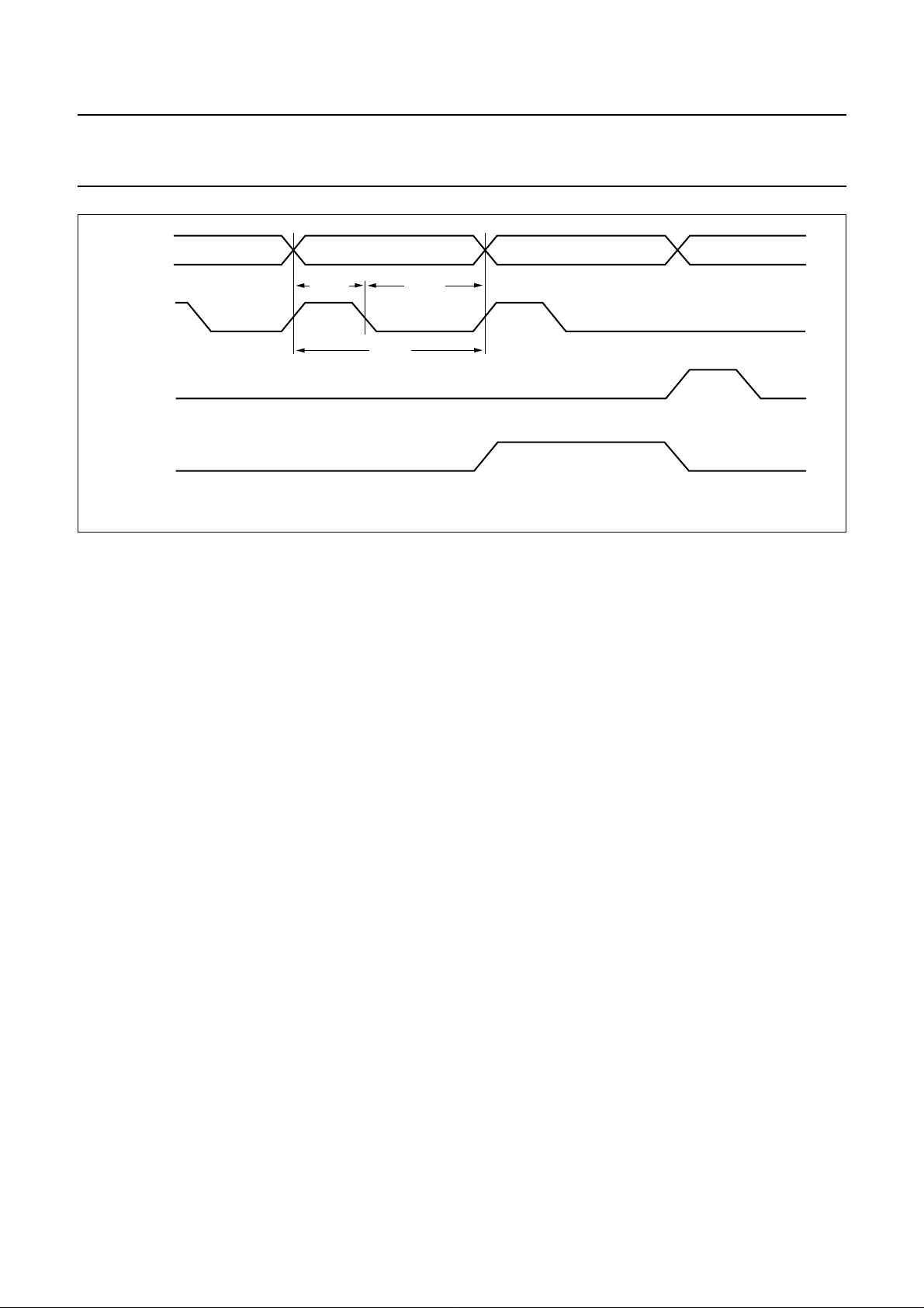
to 9 Mbytes/s. A timing diagram is shown in Fig.3. Next to
the 8-bit wide data bus an audio and video strobe is
expected at the input. Erroneous data may be flagged via
the error indicator.
AVDAT0
handbook, full pagewidth
to
AVDAT7
VSTROBE
ASTROBE
ERROR
video byte (n) video byte (n + 1) audio byte (m)
≥25 ns ≥25 ns
≥75 ns
Fig.3 Timing diagram of parallel input mode.
2001 Mar 28 11
MGD323
Page 12
Philips Semiconductors Objective specification
Integrated MPEG2 AVG decoder SAA7201
handbook, full pagewidth
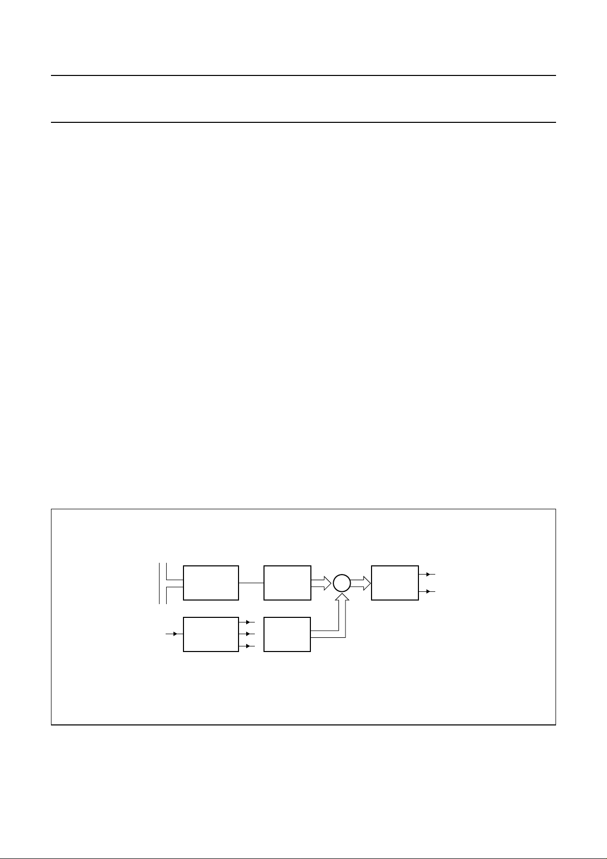
AVDAT0
to
AVDAT7
VSTROBE
ASTROBE
ERROR
video bit (n + 6) video bit (n + 7) audio bit (m + 0)
≥25 ns ≥25 ns
≥75 ns
Fig.4 Timing diagram of serial input mode.
first bit of a byte
MGD324
Alternativelydatacanbereceivedina1-bitserialformatat
rates up to 20 Mbit/s. In this mode, data is input at the LSB
input of the AV_DATA bus. Audio and video data must be
input in multiples of 8 bits. The first bit after switching from
audio to video (or the other way around) must be the first
bitof a byte since this transition will be used for the internal
bit-to-byte conversion.
Audio/video data can also be received via the CPU
interfacein8 or 16-bit mode. The peak rate is 27 Mbytes/s
in bursts of ≤128 bytes with a sustained rate up to
9 Mbytes/s. However, the MPEG bit rate is still limited to
15 Mbit/s for video and 448 kbit/s for audio.
Independent of the input mode all audio and video input
data are stored sequentially in the audio or video input
buffer area of the external memory. The audio and video
data can be either in MPEG2 PES, MPEG1 packet or ES
format.
Memory interface unit
The memory interface takes care of addressing and
control of the 16-Mbit external SDRAM. The SDRAM
should be either JEDEC compliant either the ‘lite/PC’
version.
Dueto memorycommunicationrequirements this interface
runs at 81 MHz. The SDRAM types used with the
SAA7201 should be organized as 1M × 16, split internally
in two banks, each having 2048 pages of 256 words of
16 bits.
Thetarget SDRAM typeisNEC µPD 4516161G5-A12-7FJ
(83 MHz JEDEC version) or NEC
µPD 4516421G5-A83-7FJ-PC (83 Mhz PC version).
Clock generation
The clock generation unit generates all the internal
processing clocks, the clock for the system time base
counter and the audio oversampling clock for the audio
DAC. For this purpose a non-integer divider plus a PLL is
implemented. In order to get reliable audio and video
decoding the 27 MHz input clock should be locked
externally to the MPEG time base.
Host interface system
The host interface system handles the communication
between on one side the SAA7201 plus SDRAM and on
the other side the external CPU. The interface consists of
a16-bit wide data bus plus 8 address lines.Itis compatible
with both Motorola’s 68xxx and Intel’s x86 family.
An optimized interface with the SAA7208 is also
supported. Via this interface a fast direct access to a large
number of internal status and data registers can be
achieved. Moreover, the external SDRAM can be
accessed via a specific register in combination with an
internally implemented auto increment counter.
The access to the external SDRAM is guaranteed up to a
sustained data rate of 9 Mbyte per second. However, in
practice the achievable data rate can be much higher.
Next to the data and address lines, 4 interrupt lines are
part of the host interface bus. Each interrupt line can
monitor up to 32 internal events which all can be masked
individually. Examples of internal events are audio/video
bit stream information, decoder status, internal error
conditions and input buffer occupation. The latter may be
veryuseful in interactiveapplicationsto serve as inputdata
request line.
2001 Mar 28 12
Page 13
Philips Semiconductors Objective specification
Integrated MPEG2 AVG decoder SAA7201
System time base unit
Thesystemtime base unit serves as a timing master for all
internal processes. It consists of two 24-bit wide System
Time Clock (STC) counters, running at 90 kHz. The STCs
willbe used as internalsynchronizationreference for audio
and video.The contents of the STC can be loaded by the
external CPU which should insure that the phase of the
SAA7201 internal STC is identical to the main system time
clockinthesystem demultiplexer. The CPU should correct
for possible latency problems.
Because two counters are implemented, the previous time
base reference which might still be required as reference
for some time in case of time base discontinuity, can be
maintained. Thus all information for audio/video
synchronization is available in the decoder chip and only
minor support of the external controller is required.
The synchronization of graphics for e.g. subtitling, should
be controlled by the external CPU.
Video input buffer and synchronization control
The size and position of the video input buffer in the
external SDRAM is programmable. By default 2.6 Mbit/s
are reserved for the video input buffer but in principle any
other value can be programmed. The current fullness of
thevideoinputbuffercan be monitored by the CPU and an
internal interrupt will be generated is case of either near
over- or near underflow.
Data retrieval from the input buffer can be controlled by
DTS time stamps parsed from the PES or MPEG1 packet
stream. For those frames where no DTS time stamp is
present in the video bitstream a DTS is emulated by the
SAA7201.
Obviously this emulation mode can also be used when the
input stream is a video elementary stream (ES). The latter
case should be handled by start and stop decode
commands from the CPU.
The external CPU can select to retrieve the video PES
header and/or video PES private data for further software
processing.
Audio input buffer and synchronization control
The audio input buffer and synchronization control
basically behaves identical to its video counter part.
The default buffer size is 64 kbit in this case.
Synchronization will be controlled by PTS time stamps in
theaudioPacketizedElementary Stream. Also in this case
an PTS emulation or a free running start/stop controlled
mode are supported.
Audio decoder
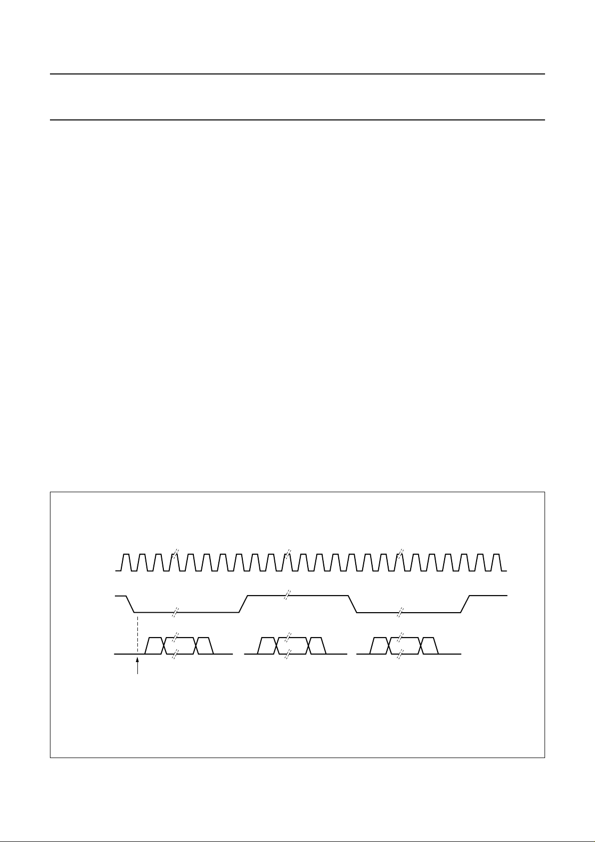
A functional block diagram for the audio decoding part is
depicted in Fig.5.
handbook, full pagewidth
DRAM-bus
81 MHz
BUFFER AND
SYNC UNIT
AUDIO
CLOCK
GENERATOR
MPEG
AUDIO
DECODER
AUDIO
BEEP
Fig.5 Audio decoding unit.
2001 Mar 28 13
+
Audio decoding unit
INTERFACE
OUTPUT
Sony or
2
S-bus
I
SPDIF
MGD325
Page 14
Philips Semiconductors Objective specification
Integrated MPEG2 AVG decoder SAA7201
Audio decoding will be performed at a clock locked to the
video decoding clock and only the output interface is
running on the audio oversampling clock.
The audio decoder unit performs the decoding of the
selected MPEG audio stream in a range from 8 up to
448 kbit/s in a fixed or variable bit rate format. Decoding is
restricted to 2 channel, layer I, II MPEG audio at sampling
frequency of 48.0, 44.1, 32.0, 24.0, 22.05 or 16.0 kHz.
The audio decoder support the stop, mute, and skip
function to support insertion
Apart from basic MPEG processing the audio decoder
core contain also:
• Support for: stop, mute and skip function.
• Fully parameterized dynamic range compression unit to
decrease the dynamic range of the output signal on
audio frame basis. Depending on the power level a
programmable amplification and offset may be applied.
• Fully programmable base band audio processing unit to
control the gain in both output channels independently
and/or to mix both channels.
• MPEG de-emphasis filtering on the output data, thus
avoiding the need of external analog de-emphasis filter
circuitry.
• Storage buffer for the last 54 bytes of each audio frame.
The CPU can retrieve eventual ancillary data from this
buffer.
The output of the audio decoder unit can be mixed with
square waveform audio signals which are generated by a
beep generator. Programmable parameters for the beep
generator are amplitude, frequency and duration.
The audio output interface module produces stereo base
band output samples on two different outputs at the same
time:
• Serial digital audio in I2S-bus or in Japanese format in
16, 18, 20 or 22-bit
• SPDIF (Sony/Philips Digital Interface).
Any of the two outputs may be enabled or set to high
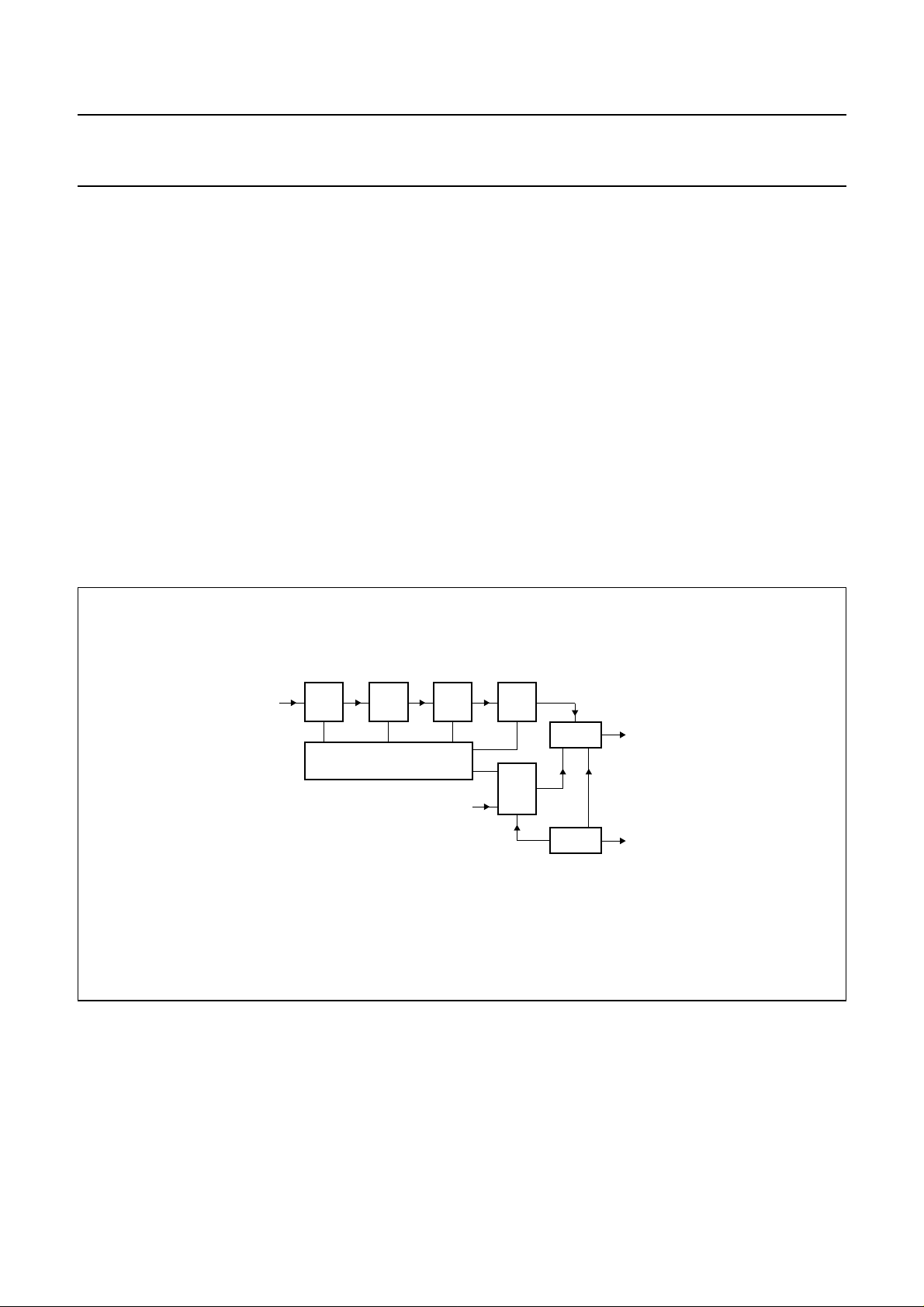
impedance mode. The I2S-bus format with 18-bit sample
precision is shown in Fig.6.
The difference between I2S-bus and the Japanese format
is that I2S-bus is MSB aligned whereas the Japanese
format is LSB aligned.
The 1-bit serial interface SPDIF contains 64-bit per audio
sample period. Complete frames must be transmitted at
the audio sample rate. Not only left/right information but
also validity flags, channel status, user data and parity
information is contained in an SPDIF frame (see Chapter
“References”).
handbook, full pagewidth
SCLK
WS
SD
0
b17
MSB aligned
31 32 63
b0
left sample n left sample n + 1right sample n
b17 b0 b17 b0
Fig.6 I2S-bus format with 18-bit sample precision.
2001 Mar 28 14
MGD326
Page 15
Philips Semiconductors Objective specification
Integrated MPEG2 AVG decoder SAA7201
Video decoder
The video decoding unit provides all actions required for
compliant decoding of MPEG2 main level, main profile
codedvideo bit streams. The decoding process consistsof
fixed and variable length decoding, run length decoding,
inverse quantization, inverse discrete cosine
transformation, motion compensation and interpolation.
In general the arithmetic decoding result is stored as
reference picture in the external memory.
Decoded B-frames are only stored for the conversion from
the frame coded macro block (MB) to the scanning line
format. In many cases a field storage is sufficient for this
conversionbutinsomecasestheusermightdecidetouse
afull frame storage to enable chroma frameup-conversion
or full performance 3 : 2 pull-down in 60 Hz systems.
Obviously when using less memory for the video decoding
process more memory is available for non-video decoding
tasks.
The Frame Buffer Management unit (FBM) manages the
allocation of frame buffers in external SDRAM for both
video decoding and display unit and can be programmed
to use less memory in not fully MP@ML bitstreams:
smaller pictures (e.g. 544 × 576), simple profile, etc.
Apart from decoding compliant MPEG video streams the
decoder deals with some trick modes. Supported are field
or frame freeze at I or P pictures or freeze field on
B-pictures. In the latter case decoding will continue as a
background process and the output can be restarted at
any moment. When receiving non-compliant MPEG
streams the decoder can be switched to a scanning mode
in which only I or I + P frames are decoded while skipping
all other pictures. In the single step mode, the decoder
decodes just one frame and awaits a next step command.
Thefunctional diagram of the video decoding unit is shown
in Fig.7.
handbook, full pagewidth
from
input
buffer
VLD
IZZ IQ IDCT
FLD
from reference
memory
MC
Fig.7 Video decoding unit.
INTERP
FBM
to external
memory
to display
unit
MGD327
2001 Mar 28 15
Page 16
Philips Semiconductors Objective specification
Integrated MPEG2 AVG decoder SAA7201
Graphics unit
The SAA7201 incorporates the display support for pixel
based graphics. Possible applications are the user
interface, logos and subtitling. Graphical data should be
grouped logically in regions and will be displayed in boxes
at the screen.
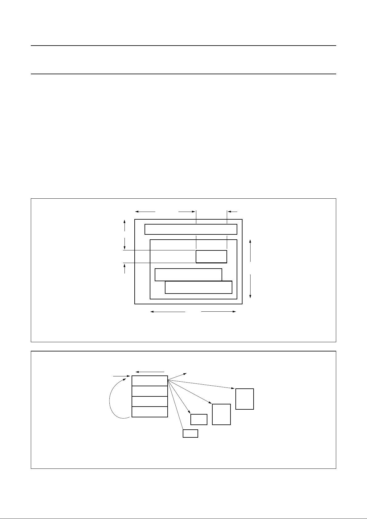
The definition of each region in the decoder consists of
four parts being a region descriptor, a top-field descriptor,
a bottom-field descriptor and a table-data descriptor:
• The region descriptor contains information relevant for
the full region like format, size, position and pointers to
the other descriptors.
handbook, full pagewidth
REGION-1 (VBI-SIGNALS)
V-start (2)
V-size (2)
REGION-3 (256 ENTRY CLUT)
• The top-field and bottom-field descriptor contain a pixel
based bit-map for the contents of that region for both
fields independently. The bit-maps can be stored in
either straight forward or in a compressed bit-map
format.
• The table-data descriptor defines the tables to be used
for the transformation of bit-maps to display colours.
All descriptors should be loaded under control of the
external CPU in the external memory.
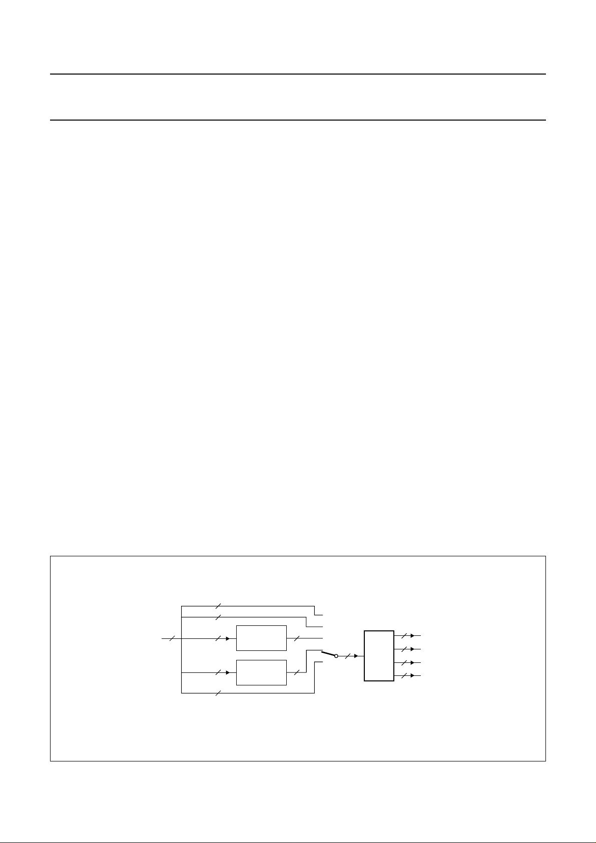
The appearance of graphical data at the display is
determined by the assembly of region descriptors in a so
called display list. An example of such a display list for the
4 regions example is shown in Fig.9.
H-size (2)H-start (2)
REGION-2
active
video
handbook, full pagewidth
gfx
anchor
address
eodl
Fig.8 Graphics unit.
128 bit
DESCRIPTOR 1
DESCRIPTOR 2
DESCRIPTOR 3
DESCRIPTOR 4
Fig.9 Display list.
REGION-4
table
data
active
video
position, size, format
pointers to locations in SDRAM
PIXEL
CLUT
MAP
DATA
top-field
MGD328
PIXEL
DATA
bottom-field
MGD329
2001 Mar 28 16
Page 17
Philips Semiconductors Objective specification
Integrated MPEG2 AVG decoder SAA7201
Basically there is no restriction on the number of different
regions but because regions may not vertically overlap the
practical limit will be the number of lines within a field.
However, one should realize that each region requires its
own 128-bit region descriptor.
The display list will be scanned twice per frame, once for
each display field. The region descriptors should be
ordered properly in the external SDRAM, starting from the
graphics anchor address. The last descriptor in the list
must have the end of display list indicator set.
Multiple pixel bit-maps, CLUTs and map tables may be
stored in the external memory but per region only two
bit-maps (one for each fields) and two tables
(CLUT + map table)may be used. Obviously bit-maps and
tables may be shared by multiple regions.
Pixel data bit-maps can be described in 2, 4 or 8 bit/pixel
ineithera direct bit-map or coded in a one-dimensional (H)
variable and run length encoded format according the
pixel-data-sub-block syntax as specified in Chapter
“References” and illustrated in Chapter “Appendix”.
The actual coding format is specified in the region
descriptor for each region thus allowing different coding
schemes within a picture.
During display the 2, 4 and 8 bit/pixel bit-maps will be
transformed, eventually with run length decoding, via a
table look-up mechanism into a 4, 16 or 256 different YUV
colours with 8-bit resolution for each component plus a
factor T for mixing of graphics and MPEG video.
In order to obtain maximum flexibility two cascaded tables
are active in this bit-map to pixel conversion as indicated
in Fig.10.
The tables are retrieved from the external memory just
before the region is going to be displayed. One table per
region can be updated and for small tables this occurs
during the horizontal blanking interval. However, updating
a 256 entry CLUT may take about one line period which
means that a spatial separation of one line with the
previous region is mandatory in this case. If the required
tables for a certain region are already stored in the local
memory, the table down load action can be skipped.
Additionally some special bits can be set in the region
descriptor.
• Transparency shift: this parameter overrules the pixel
based transparency in order to support fading of the
entire graphical region.
• Zoom:this parameter initiates horizontal pixel repetition.
It should be noted that a copy of pixels in vertical
directioncan be achieved by pointing to a single bit-map
for both fields.
Regions can also be defined in the vertical blanking
interval. In combination with 8 bit/pixel coding, arbitrary
test signals on 13.5 MHz grid can be programmed.
Possible application areas are teletext, closed caption,
wide screen signalling bits, Video Programming Signals
(VPS) and Vertical Interval Test Signals (VITS).
As indicated above multiple regions can be specified in a
displaylist which will be scanned sequentially every frame.
In case of stationary graphics no updates of the display list
are required, but the external CPU can update it
dynamically to achieve scrolling and/or fading of one or
more graphical boxes. The display list mechanism also
allows for non real time transfer of large bit-maps by
keeping that region out of the display list during loading.
handbook, full pagewidth
8 LSBs
4 LSBs
8
4 LSBs
2 LSBs
2 LSBs
MAP
TABLE 4 to 8
MAP
TABLE 2 to 8
8
8
Fig.10 Bit-map to pixel conversion.
2001 Mar 28 17
8
Y
8
8
CLUT
8
8
U
V
T
MGD330
Page 18

Philips Semiconductors Objective specification
Integrated MPEG2 AVG decoder SAA7201
CURSOR PROCESSING
Additionally to the above defined graphics boxes one
cursor can be activated on the screen. Since the cursor
data is fully stored locally, no overlapping restriction apply
to this box so the cursor can moved over the entire screen.
The cursor can be as large as 1 kpixel with a 2 bits/pixel
colourdepth. Obviously data transfer can be done on DMA
basis and need only be performed when a cursor is
required or when its contents must be modified.
The cursor XY dimensions (where the Y dimension refers
to frame lines) can be selected between 8 × 128, 16 × 64,
32 × 32, 64 × 16 and 128 × 8. On top of these shapes, a
zoom with a factor 2 can be applied in both directions
independently.
The cursor pixels will be translated via a 4-entry CLUT to
YUV colours and a transparency factor T. The resolution
of the YUV parameters is 6, 4, 4 bits respectively.
The T parameter is coded in 2 bits to enable the mixing
with video and graphics in 4 steps being 100% (cursor
only), 50%, 25% and 0% (fully transparent cursor).
Display unit
Before feeding the MPEG decoded and graphical data to
the output, a display unit re-formats the MPEG specific
4:2:0 format to CCIR-601 4 : 2 : 2 format and performs
a mixing between video and graphics where required.
The output picture can be up to 720 × 576 pixels at 50 Hz
or 720 × 480 pixels at 60 Hz.
A schematic representation of this unit is shown in Fig.11.
• In a first step a selected window can be retrieved from
the decoded MPEG data. This might be useful for e.g.
pan and scan operations for aspect ratio conversion.
• In case the resulting number of pixels per line does not
match the 720 pixels/line output format a horizontal
scaler can be activated. This scaling unit can transform
any number of bits below 720 to the required output
format. Internally a poly-phase filter is used which
performs a 64 phases interpolation. Not only
up-conversion but also down-conversion is supported
up to a scaling by a factor 2. Thus horizontal scaling can
be performed in a range from 0.5 up to 64. In practice
the maximum up-conversion factor will be less or equal
to 4.
• In vertical direction the picture can be expanded or
scaleddown, in both cases byafactor 2. Expansion with
a factor 2 might be relevant for the up-conversion of SIF
resolution pictures to full screen. The factor 2 scaling, if
combinedwith theappropriatehorizontal scaling, results
is1⁄4picture thus freeing-up a large screen area for
graphics. This might be very useful for electronic
program guide applications. It should be noted that in
caseofpicturecompression an anti-aliasing filter can be
activated.
• Shifting: when the resulting MPEG picture is smaller
thanthe720 × 576 (480) displayformat,thispicturecan
be located anywhere on the display screen.
Moreover, the non-covered area can be given any
background colour.
• Clipping: the amplitude of the MPEG decoded and
re-scaled video signal is kept within the range 16 to 235
for luminance and 16 to 240 for both chrominance
components.
handbook, full pagewidth
MPEG
decoded
picture
WINDOW
EXTRACTION
CHROMA
UP-CONVERSION
SCALING
64 STEP
MIXER
GRAPHICS CURSOR
Fig.11 Display unit.
2001 Mar 28 18
SHIFTING CLIPPING
4 STEP
MIXER
OUTPUT
FORMAT
MGD331
to digital
CVBS
encoder
Page 19
Philips Semiconductors Objective specification
Integrated MPEG2 AVG decoder SAA7201
• The chroma up-conversion unit converts the MPEG
4:2:0format into the at the output required
4:2:2format.This vertical up-conversion is performed
by a simple 8-phase interpolation between two adjacent
lines.
• Themixer units combine MPEG video with graphics and
cursor information in two steps. In a first step the MPEG
decodedinformation ismixedwith graphical information.
Mixing can be done at pixel basis in 64 steps and is
controlled by the internally implemented colour look up
table. In a second step, the video plus graphics can be
mixed in 4 steps with the internally generated cursor.
• The output formatting unit performs two main tasks, i.e.
synchronization and formatting. Synchronization is
characterized by three signals being horizontal (H),
vertical (V) and field parity (FP), all having
programmable length and polarity.
handbook, full pagewidth
CLK
Since the decoder can operate in master or slave mode,
the synchronization signals can be generated by the
decoder or should be delivered by an external device.
In both cases the length and polarity should be
programmed internally.
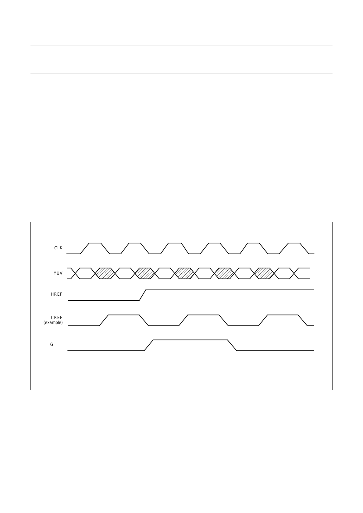
The video output samples are supplied in a multiplexed
YUV format to the output. Next to this byte wide YUV
stream, which can directly be supplied to most
commercially available composite video encoder ICs,
three additional signals are delivered at the output.
HREF indicates all active samples; CREF can flag any
combination of pixels: U, V, Y
and/or Y
odd
even
; GRPH
flags all the pixels inside a graphical box.
Additionally the full YUV bus can be set to a HIGH
impedance state under control of the signal YUV_ENA.
This might be useful for multiplexing the MPEG decoder
output with any other signal source on static basis.
YUV
HREF
CREF
(example)
GRPH
'128' '16'
Fig.12 Timing diagram of graphics information output.
U
0
Y
0
V
0
Y
2
MGD332
2001 Mar 28 19
Page 20

Philips Semiconductors Objective specification
Integrated MPEG2 AVG decoder SAA7201
JTAG
The SAA7201 supports the standard Boundary Scan test
instructions: bypass, extest, sample, intest, runbist,
idcode.
Memory requirements
As indicated before the MPEG source decoder operates
with 16 Mbit of external memory. Several processes
require access to the external memory, mostly being the
video decoding process. In normal main level, main profile
video applications about 1.2 Mbit of memory space is free
for non-video processes. In practice most of this capacity
will be used for graphics. In combination with the internal
variable length decoding, full screen graphics at 8-bit per
pixel is feasible. Moreover, by having introduced a flexible
memory allocation procedure the available memory
capacity for graphics may be enlarged when decoding
lower resolution MPEG pictures or when the input bit rate
is less than 15 Mbit/s.
Table 1 Required memory capacity for some user defined modes
System 50 Hz 60 Hz
Bit rate (R) 15 Mbit/s 15 Mbit/s 9 Mbit/s
Obviously for graphics-only applications all 16 Mbit can be
used for the storage of bit-maps and look-up tables.
In Table 1 an overview is given of the required memory
capacity for some user defined modes.
In 50 Hz systems memory capacity can be saved by
restricting the chroma vertical interpolation to field
interpolation. This mode would only bring some extra
chroma resolution in case the input stream contains
progressive coded pictures.
In 60 Hz systems the reduction of storage capacity for
B-frames to field capacity has not only consequences for
the chroma vertical interpolation but also for the
3 : 2 pull-down operation mode. The operation
repeat-first-field is not possible in all cases and a modified
3 : 2 pull-down is performed under the control of the
SAA7201. The user may decide to use this modified
3 : 2 pull-down mode in order to have more memory
available for OSD or graphics.
Chroma interpolation frame field field frame field field
3 : 2 pull-down n.a. n.a. n.a. full MPEG modified modified
Picture format 720 × 576 720 × 576 544 × 576 720 × 480 720 × 480 720 × 480
Audio input buffer 64 kbit 64 kbit 64 kbit 64 kbit 64 kbit 64 kbit
Video input buffer 1835 kbit 1835 kbit 1835 kbit 1835 kbit 1835 kbit 1835 kbit
Video implementation buffer (R/P) 600 kbit 600 kbit 400 kbit 500 kbit 500 kbit 300 kbit
Slave synchronization buffer (R/2P) 300 kbit 300 kbit 200 kbit 250 kbit 250 kbit 150 kbit
Reference and decoded picture 13456 kbit 12719 kbit 9609 kbit 12441 kbit 10634 kbit 8042 kbit
Total for video + audio 16255 kbit 15518 kbit 12108 kbit 15090 kbit 13292 kbit 10391 kbit
Remains for OSDG (2
24
= 16777 kbit) 522 kbit 1259 kbit 4669 kbit 1687 kbit 3485 kbit 6386 kbit
2001 Mar 28 20
Page 21
Philips Semiconductors Objective specification
Integrated MPEG2 AVG decoder SAA7201
LIMITING VALUES
In accordance with the Absolute Maximum Rating System (IEC 60134).
SYMBOL PARAMETER CONDITIONS MIN. MAX. UNIT
V
DD
V
max
P
tot
T
stg
T
amb
THERMAL CHARACTERISTICS
SYMBOL PARAMETER VALUE UNIT
R
th j-a
supply voltage (on all supply pins) 3.0 3.6 V
maximum voltage on all pins 0 5.5 V
total power dissipation T
=25°C − tbf W
amb
storage temperature −55 +150 °C
operating ambient temperature 0 +70 °C
thermal resistance from junction to ambient in free air 30 K/W
2001 Mar 28 21
Page 22
Philips Semiconductors Objective specification
Integrated MPEG2 AVG decoder SAA7201
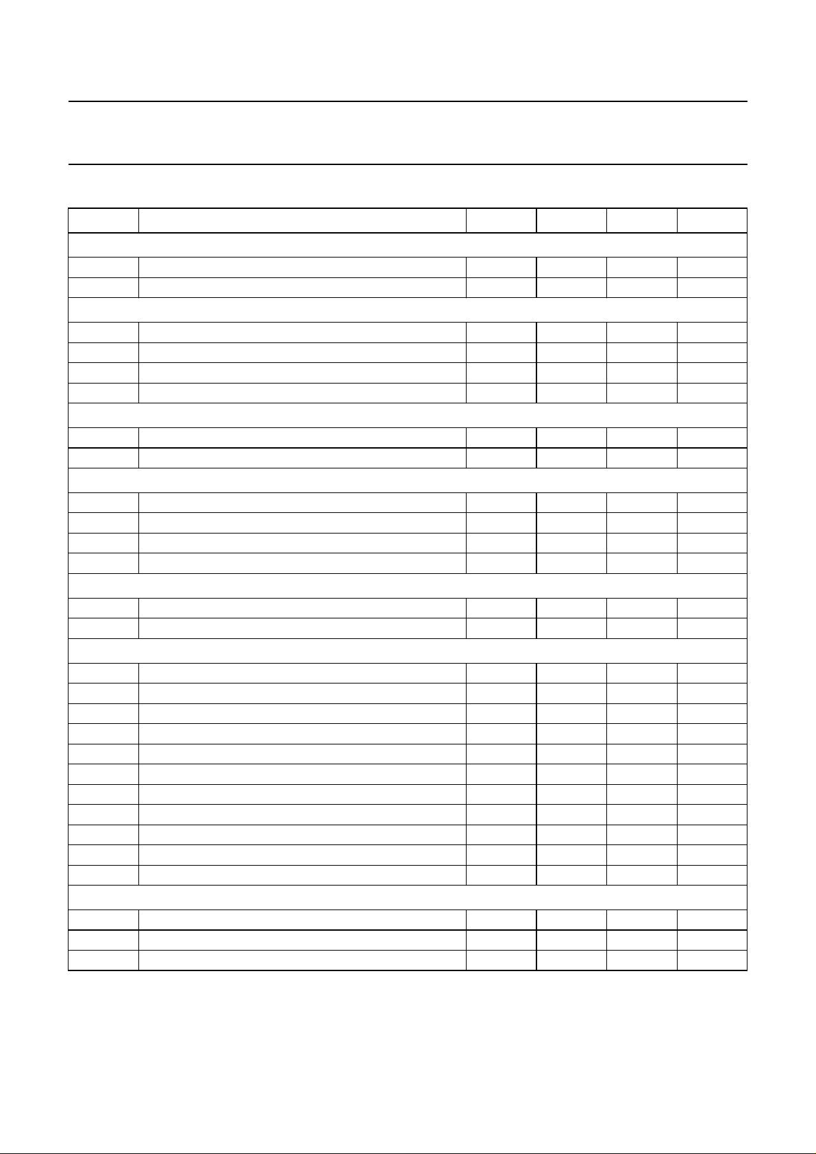
CHARACTERISTICS
SYMBOL PARAMETER MIN. TYP. MAX. UNIT
Supply
V
DD
I
DD
Inputs
V
IH
V
IL
I
LI
C
i
Outputs
V
OH
V
OL
CLK timing
T
C
δ duty factor 40 − 60 %
t
r
t
f
Input timing with respect to CLK rising edge
t
su
t
h
Timing (see Figs. 13, 14, 15, 16, 17, 18, 19, 20, 21, 21 and 21)
t
su(A-CS)
t
h(A-CS)
t
su(D-W)
t
su(D-R)
t
rel(D)
t
h(CT)
t
W(ACK)
t
rel(ACK)
t
d(ACK-R)
t
d(ACK-W)
t
W(RW)
Output timing with respect to CLK rising edge
t
h
t
d
C
L
supply voltage 3.0 3.3 3.6 V
supply current − tbf − mA
HIGH level input voltage 2.0 − VDD+ 2.0 V
LOW level input voltage −0.5 − 0.8 V
leakage current −−20 mA
input capacitance 0 − 10 pF
HIGH level output voltage 2.4 −−V
LOW level output voltage −−0.4 V
cycle time 37.036 37.037 37.038 ns
rise time 2 − 4ns
fall time 2 − 4ns
set-up time 8 −−ns
hold time 0 −−ns
address/CS set-up time 20 −−ns
address/CS hold time 75 −−ns
data write set-up time 20 −−ns
data read set-up time 20 −−ns
data release time 0 − 10 ns
control signal hold time 0 −−ns
acknowledge pulse width 25 −−ns
acknowledge release time 0 − 10 ns
delay time for acknowledge read 96 − 125 ns
delay time for acknowledge write 48 − 75 ns
write/read pulse width 25 −−ns
hold time 3 − t
delay time t
h
− 20 ns
d
ns
load capacitance 10 − 30 pF
2001 Mar 28 22
Page 23
Philips Semiconductors Objective specification
,,
,,
Integrated MPEG2 AVG decoder SAA7201
handbook, full pagewidth
CPADDR1
CPADDR8
DS
(Intel RDN)
DTACK
(Intel RDY)
CPDAT0
CPDAT15
to
to
CS
R/W
ADDRESS
t
su(A-CS)
t
su(D-DS)
DATA
t
h(A-CS)
t
h(D-DS)
t
d(ACK-W)
t
W(RW)
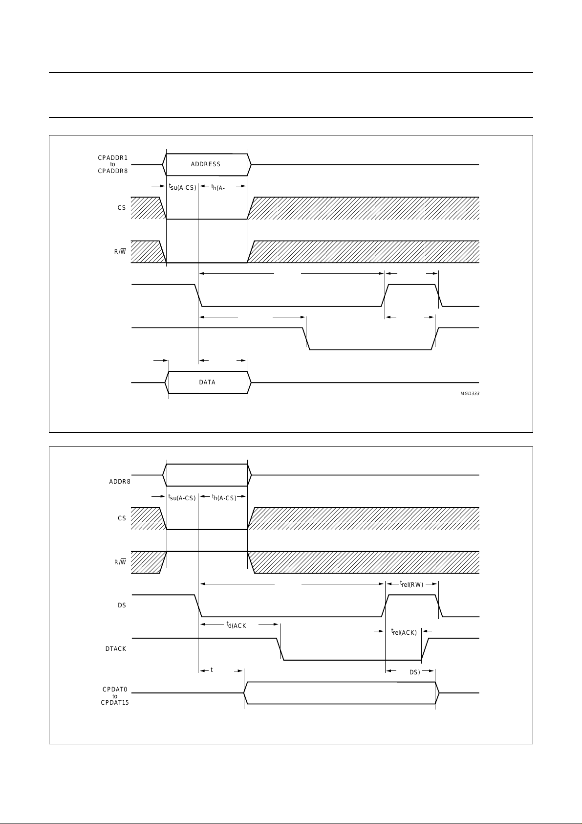
Fig.13 Motorola write timing (non-multiplexed).
t
rel(R/W)
t
rel(ACK)
MGD333
handbook, full pagewidth
CPADDR1
CPADDR8
DTACK
CPDAT0
CPDAT15
to
R/W
to
CS
DS
ADDRESS
t
su(A-CS)
t
h(A-CS)
t
A(D-R)
t
d(ACK-R)
t
W(RW)
Fig.14 Motorola read timing (non-multiplexed).
DATA
t
rel(RW)
t
rel(ACK)
t
rel(DS)
MGD334
2001 Mar 28 23
Page 24
Philips Semiconductors Objective specification
Integrated MPEG2 AVG decoder SAA7201
handbook, full pagewidth
CPADDR1
to
CPADDR8
ADDRESS
CS
R/W
(Intel NRN)
DTACK
(Intel RDY)
CPDAT0
to
CPDAT15
handbook, full pagewidth
CPADDR1
to
CPADDR8
t
su(A-CS)
t
su(D-DS)
t
h(A-CS)
t
W(RW)
t
d(ACK-W)
t
rel(ACK)
t
h(D-DS)
DATA
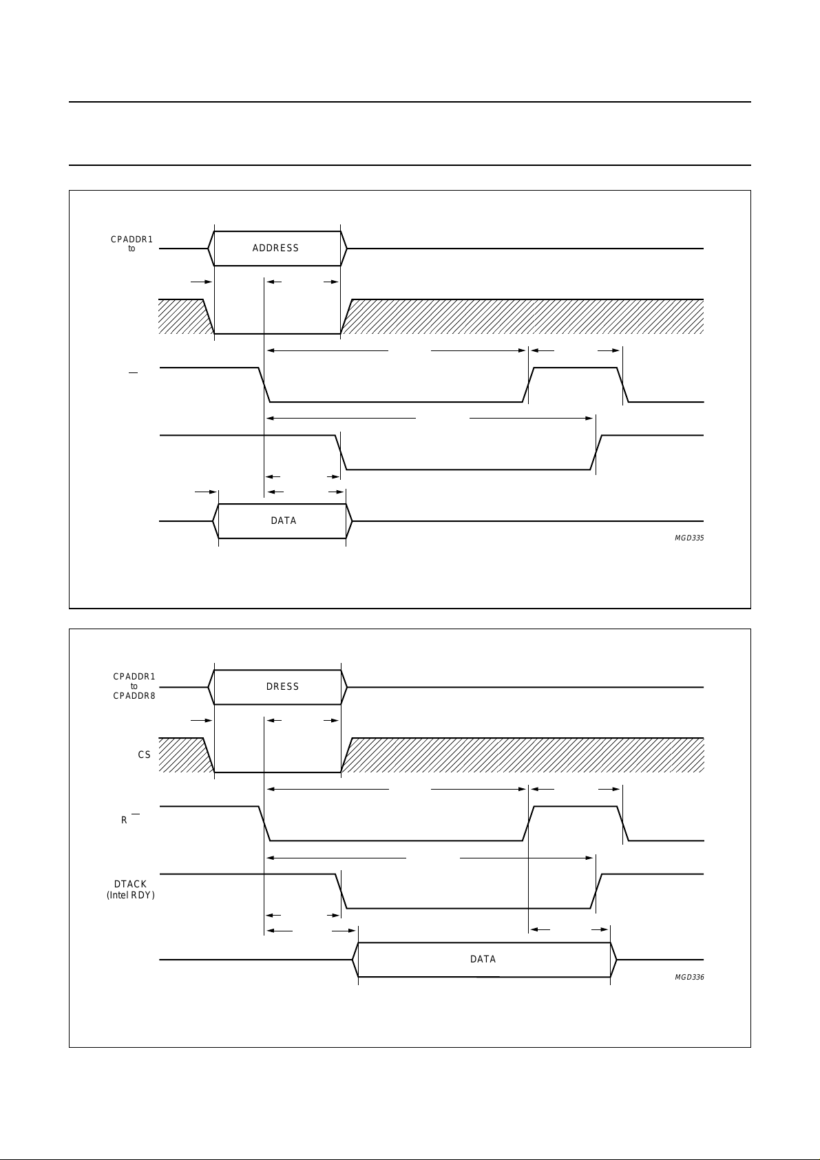
Fig.15 Intel write timing (non-multiplexed).
ADDRESS
t
rel(RW)
MGD335
CS
R/W
(Intel NRN)
DTACK
(Intel RDY)
CPDAT0
to
CPDAT15
t
su(A-CS)
t
h(A-CS)
t
rel(ACK)
t
A(D-R)
t
W(RW)
Fig.16 Intel read timing (non-multiplexed).
2001 Mar 28 24
t
d(ACK-R)
DATA
t
rel(RW)
t
rel(DS)
MGD336
Page 25
Philips Semiconductors Objective specification
Integrated MPEG2 AVG decoder SAA7201
handbook, full pagewidth
CS
DMAREQ
DMAACK
DMARDY
CPDAT0
to
CPDAT15
handbook, full pagewidth
CS
t
su(A-CS)
t
su(D-DS)
DATA
t
h(A-CS)
t
h(D-DS)
t
W(RW)
t
d(ACK-W)
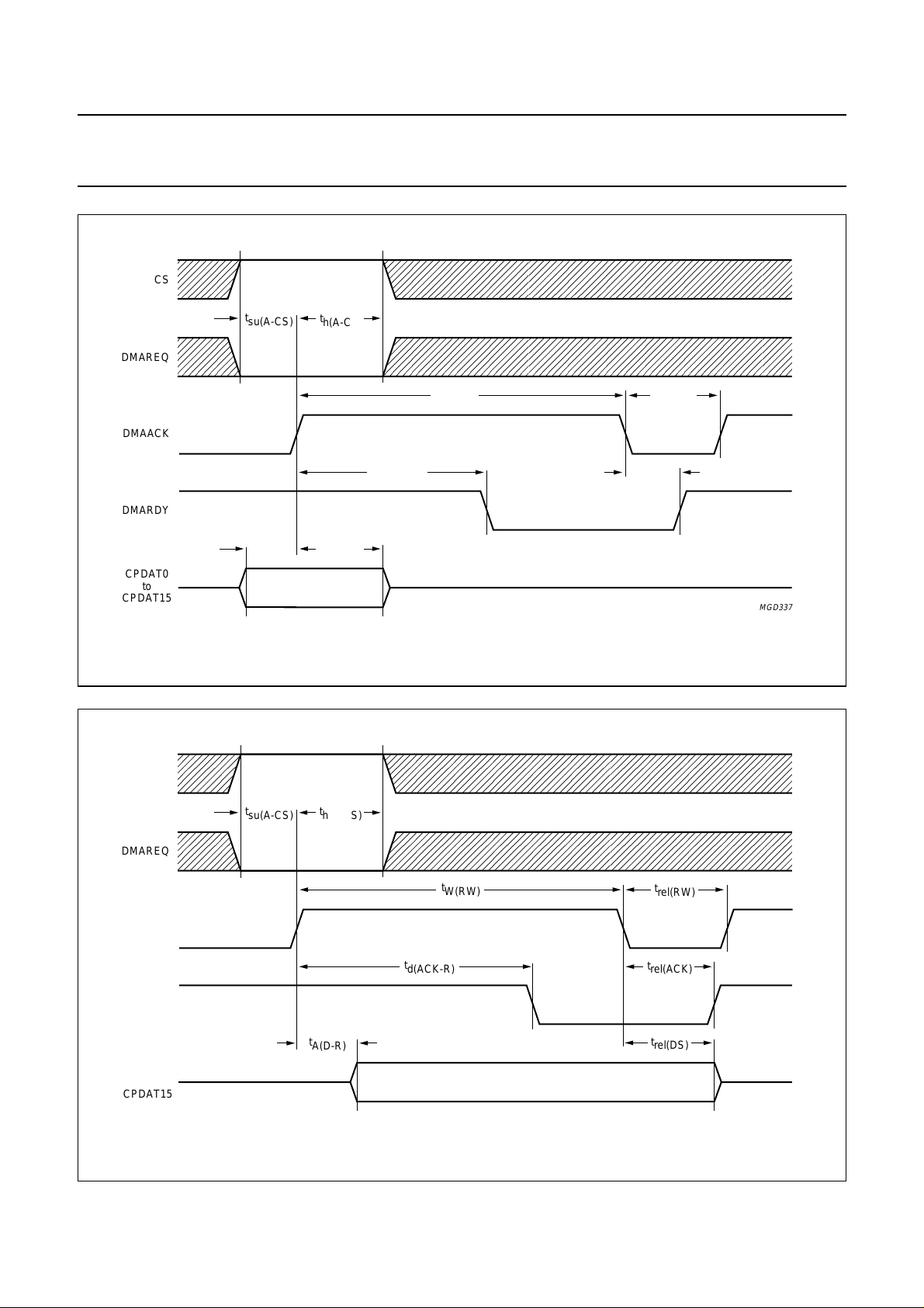
Fig.17 DMA read access.
t
rel(RW)
t
rel(ACK)
MGD337
t
h(A-CS)
t
A(D-R)
t
d(ACK-R)
t
W(RW)
DMAREQ
DMAACK
DMARDY
CPDAT0
to
CPDAT15
t
su(A-CS)
Fig.18 DMA write access.
2001 Mar 28 25
DATA
t
rel(RW)
t
rel(ACK)
t
rel(DS)
MGD338
Page 26
Philips Semiconductors Objective specification
,,
,,
Integrated MPEG2 AVG decoder SAA7201
handbook, full pagewidth
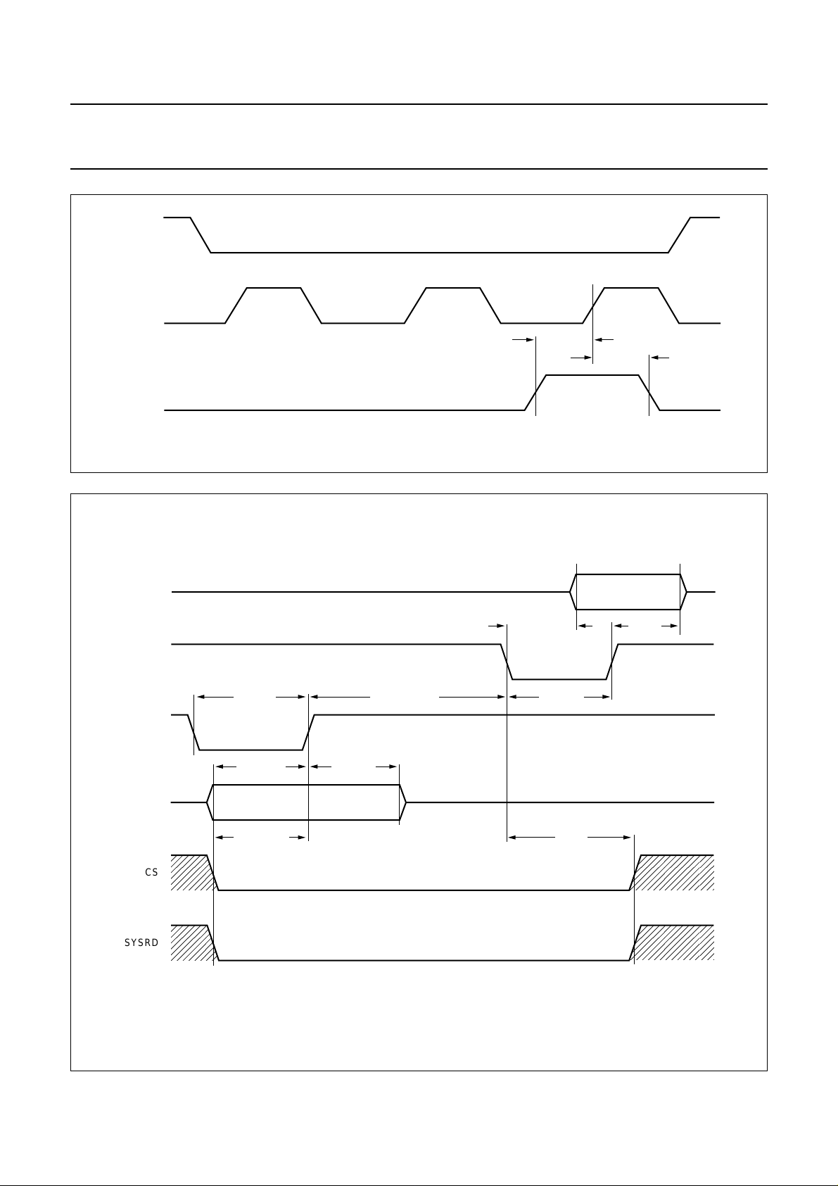
DMAREQ
DMAACK
t
su(A-CS)
t
h(A-CS)
DMADONE
MGD339
Fig.19 DMA_DONE timing.
handbook, full pagewidth
DATA
(15 to 0)
RDY
ALE
ADDRESS
(8 to 0)
CS
SYSRD
t
W(ALE)
t
su(A-CS)
t
h(CS-ALE)
t
h(A-CS)
ADDRESS
t
su(ALE-SDR)
t
su(SDR-D)
t
W(SDR)
t
h(CS)
DATA
t
rel(D)
MGD919
Fig.20 SAA7208 mode; read timing.
2001 Mar 28 26
Page 27
Philips Semiconductors Objective specification
Integrated MPEG2 AVG decoder SAA7201
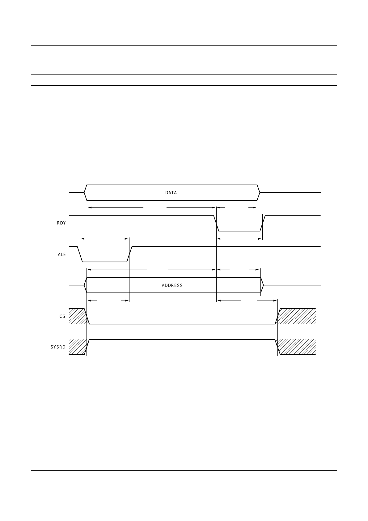
handbook, full pagewidth
DATA
(15 to 0)
RDY
ALE
ADDRESS
(8 to 0)
CS
SYSRD
t
W(ALE)
t
h(CS-ALE)
t
W(D-SDR)
t
su(A-CS)
DATA
ADDRESS
t
h(D-SDR)
t
W(SDR)
t
h(A-CS)
t
h(CS)
MGD918
Fig.21 SAA7208 mode; write timing.
2001 Mar 28 27
Page 28
Philips Semiconductors Objective specification
Integrated MPEG2 AVG decoder SAA7201
handbook, full pagewidth
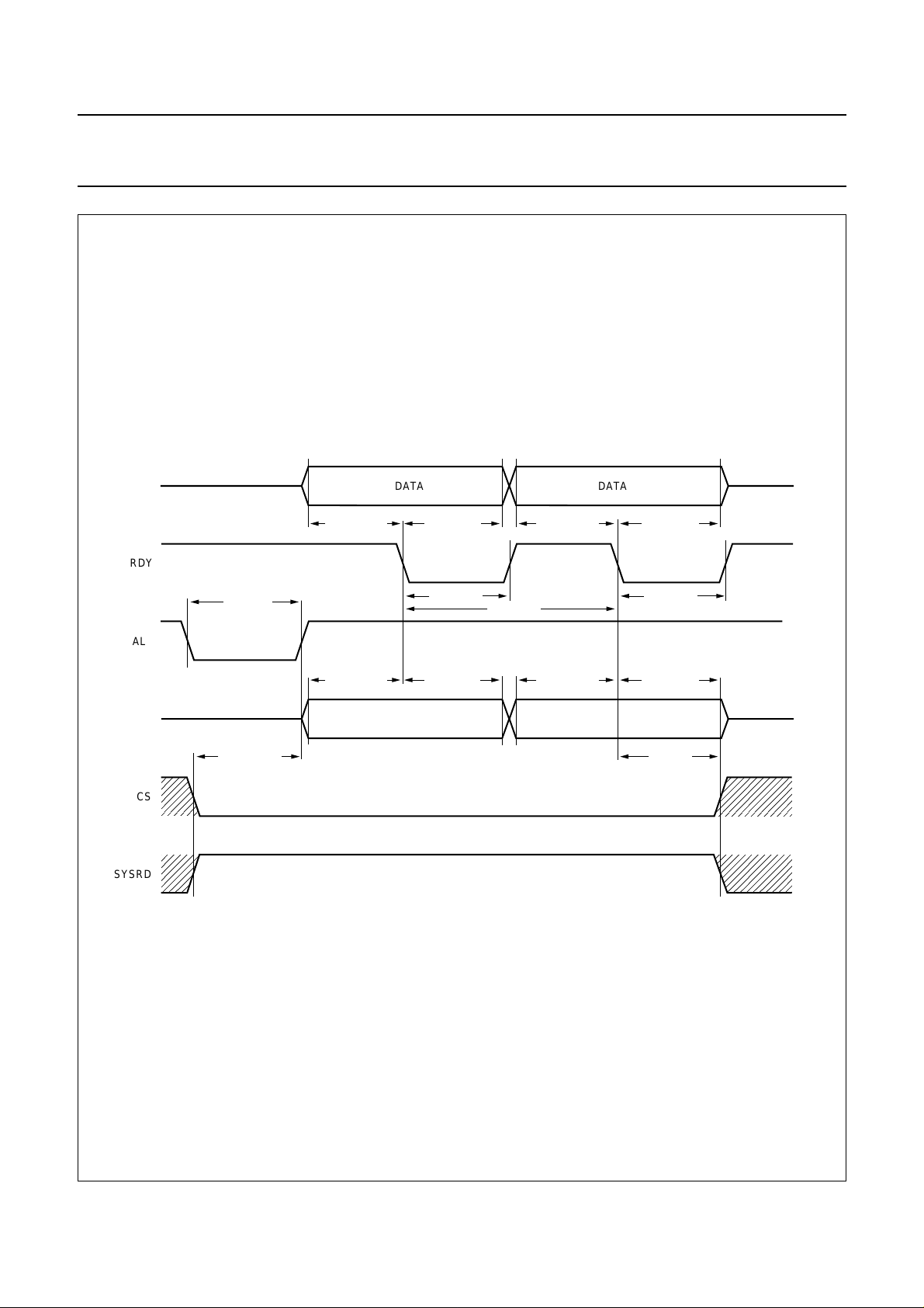
DATA
(15 to 0)
DATA DATA
RDY
ALE
ADDRESS
(8 to 0)
CS
SYSRD
t
W(ALE)
t
h(CS-ALE)
t
su(D-SDR)
t
su(A-SDR)
ADDRESS ADDRESS
t
h(D-SDR)
t
W(SDR)
t
h(A-SDR)
t
rel(SDR)
t
su(D-SDR)
t
su(A-SDR)
t
h(D-SDR)
t
W(SDR)
t
h(A-SDR)
t
h(CS)
MGD920
Fig.22 SAA7208 mode; burst write timing.
2001 Mar 28 28
Page 29
Philips Semiconductors Objective specification
Integrated MPEG2 AVG decoder SAA7201
handbook, full pagewidth
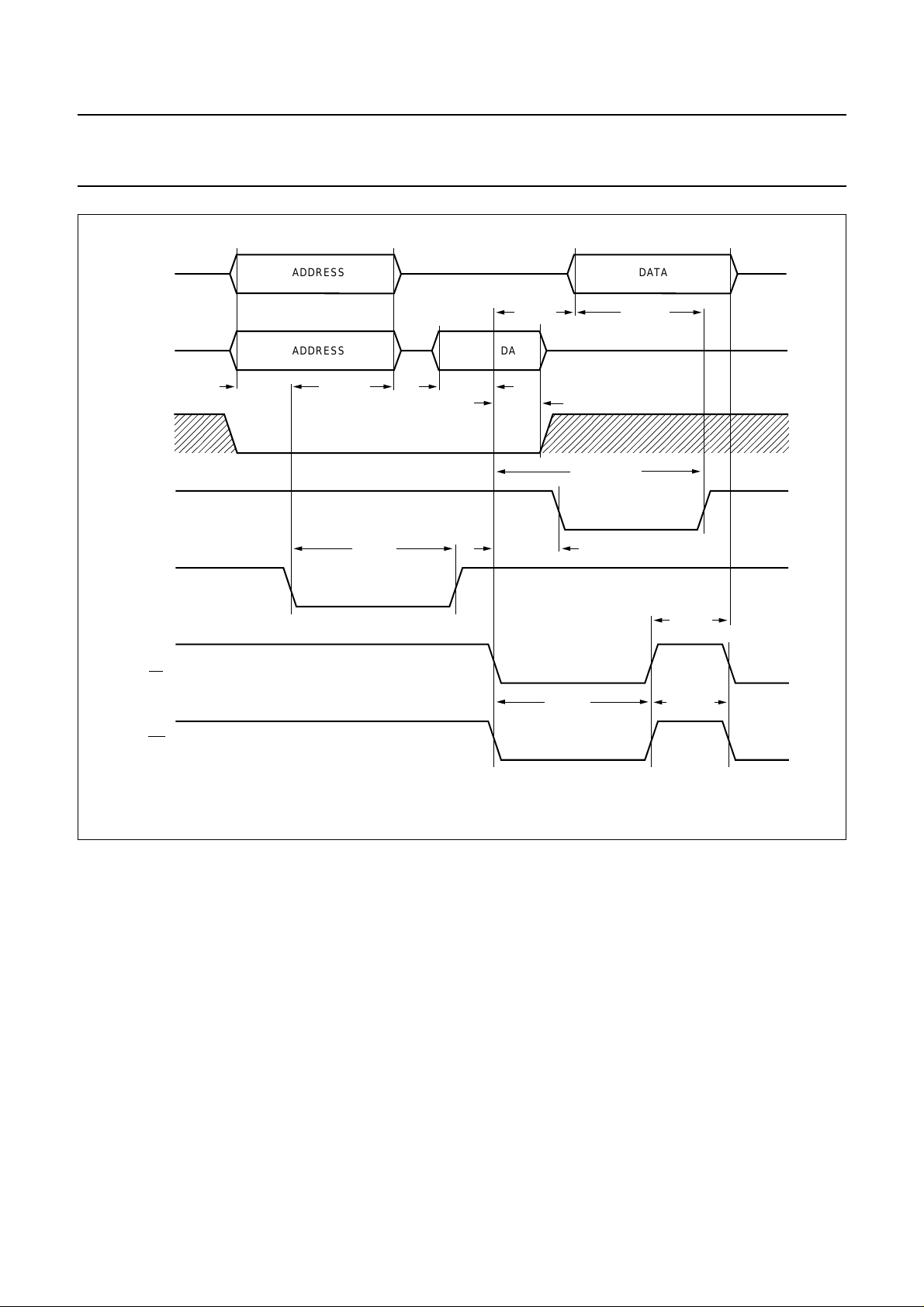
AD (read)
ADDRESS
DATA
AD (write)
CS
DTACK
(Intel RDY)
AS
(Intel ALE)
DS
(Intel RD)
WR
t
su(A-CS)
ADDRESS
t
h(A-CS)
t
W(AS)
t
su(D-DS)
t
A(D-R)
DATA
t
h(D-DS)
t
rel(ACK)
t
W(RW)
t
d(ACK-R/W)
t
su(D-R)
t
rel(DS)
t
rel(RW)
MGD341
Fig.23 Intel read/write timing multiplexed.
REFERENCES
1.
MPEG ISO/IEC 11172-1 International standard; MPEG-1 systems.
2.
MPEG ISO/IEC 13818-1 International standard; MPEG-2 systems.
3.
MPEG ISO/IEC 11172-2 International standard; MPEG-1 Video.
4.
MPEG ISO/IEC 13818-2 International standard; MPEG-2 Video.
5.
MPEG ISO/IEC 11172-3 International standard; MPEG-1 Audio.
6.
MPEG ISO/IEC 13818-3 International standard; MPEG-2 Audio.
7.
DVB subtitling system; working draft 2.0; TM 1398 rev 2
.
2001 Mar 28 29
Page 30
Philips Semiconductors Objective specification
Integrated MPEG2 AVG decoder SAA7201
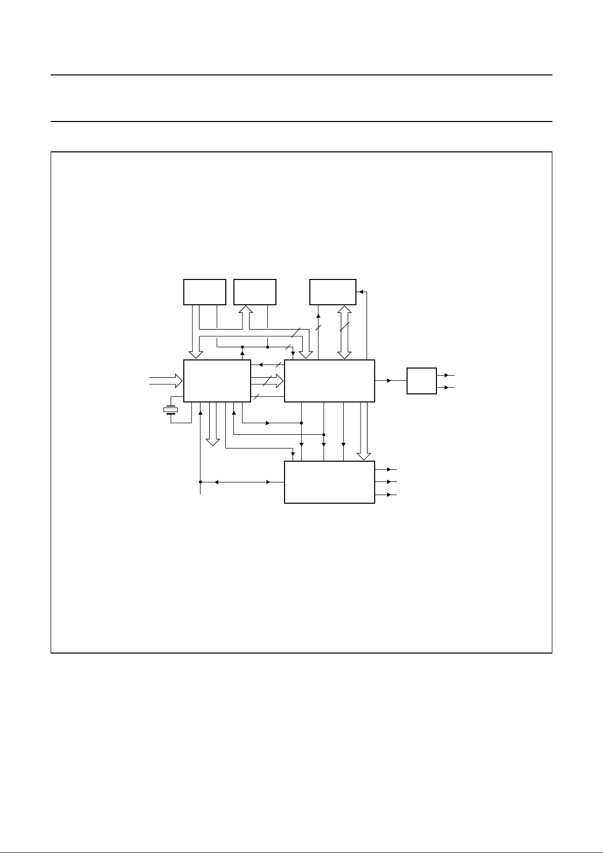
APPLICATION INFORMATION
handbook, full pagewidth
27
MHz
4 Mbits
EPROM
SAA7208
(DEMUX/MIPS)
high
speed
data
2
I
C-bus
4 Mbits
DRAM
8 + 3
IRQ
8
strobe
2
27 MHz
H, V, FP
TTX/TTXRQ
16 Mbits
SDRAM
address data control
12
16
4
16
SAA7201
H,V valid YUV
SAA7183
(EURO-DENC)
2
I
C-bus
CVBS
Y/C
RGB
AUDIO
D/A
MGD342
Fig.24 Application diagram.
2001 Mar 28 30
Page 31

Philips Semiconductors Objective specification
Integrated MPEG2 AVG decoder SAA7201
APPENDIX
Syntax of pixel-data-sub-block
data type pixel-code-string of N-coded words end of string
2 bit/pixel 01 1 pixel in colour 1
10 1 pixel in colour 2
0001 0000 11 1 pixel in colour 3 00 00 00
00 01 1 pixel in colour 0
00 00 01 2 pixels in colour 0
00 1L LL CC L pixels (3 to 10) in colour C
00 00 10 LL LL CC L pixels (12 to 27) in colour C
00 00 11 LL LL LL LL CC L pixels (29 to 284) in colour C
4 bit/pixel 0001 1 pixel in colour 1
↓↓ ↓ ↓
0001 0001 1111 1 pixel in colour 15 0000 0000
0000 1100 1 pixel in colour 0
0000 1101 2 pixels in colour 0
0000 0LLL (L>0) L pixels (3 to 9) in colour 0
0000 10LL CCCC L pixels (4 to 7) in colour C
0000 1110 LLLL CCCC L pixels (9 to 24) in colour C
0000 1111 LLLL LL11 CCCC L pixels (25 to 280) in colour C
8 bit/pixel 00000001 1 pixel in colour 1 00000000-- --00000000
↓↓ ↓ ↓
0001 0010 11111111 1 pixel in colour 255
00000000 0LLLLLLL L pixels (1 to 127) in colour 0
00000000 1LLLLLLL CCCCCCCC L pixels (3 to 127) in colour C
2001 Mar 28 31
Page 32
Philips Semiconductors Objective specification
Integrated MPEG2 AVG decoder SAA7201
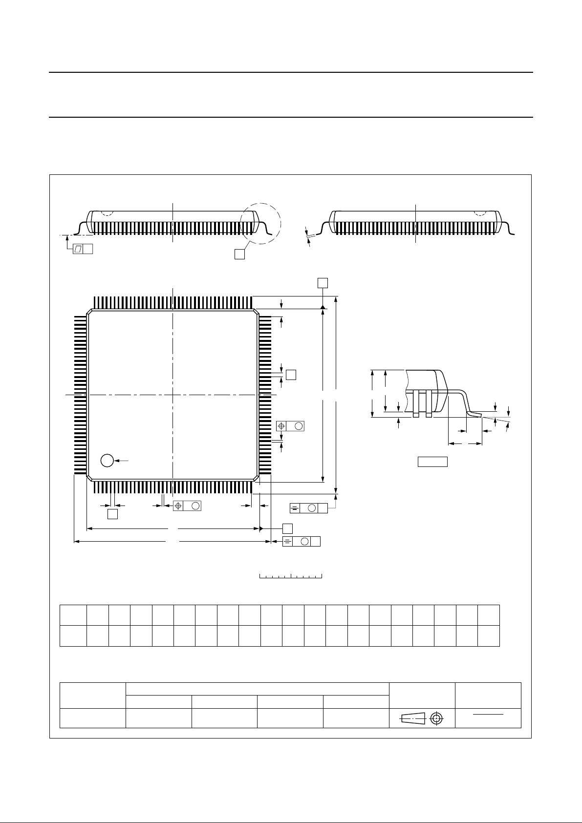
PACKAGE OUTLINE
QFP160: plastic quad flat package;
160 leads (lead length 1.95 mm); body 28 x 28 x 3.4 mm; high stand-off height
c
y
X
A
SOT322-1
120
121
pin 1 index
160
1
w M
b
3.70
3.15
0.25
p
D
H
D
cE
p
0.40
0.23
0.25
0.13
e
DIMENSIONS (mm are the original dimensions)
mm
A
max.
3.95
0.40
0.25
UNIT A1A2A3b
81
80
Z
E
e
A
p
2
A
A
1
0.15 0.1
H
E
E
w M
b
p
41
40
Z
D
0 5 10 mm
(1) (1) (1)
D
28.1
27.9
(1)
eH
28.1
0.65 0.31.95
27.9
B
scale
H
32.2
31.6
v M
D
v M
B
E
32.2
31.6
A
LL
1.1
0.7
detail X
Z
D
1.5
1.1
(A )
3
L
p
L
Zywv θ
E
o
1.5
8
o
1.1
0
θ
Note
1. Plastic or metal protrusions of 0.25 mm maximum per side are not included.
OUTLINE
VERSION
SOT322-1 MO-112
IEC JEDEC EIAJ
REFERENCES
2001 Mar 28 32
EUROPEAN
PROJECTION
ISSUE DATE
97-08-04
99-12-27
Page 33

Philips Semiconductors Objective specification
Integrated MPEG2 AVG decoder SAA7201
SOLDERING
Introduction to soldering surface mount packages
Thistext gives a very brief insight toacomplex technology.
A more in-depth account of soldering ICs can be found in
our
“Data Handbook IC26; Integrated Circuit Packages”
(document order number 9398 652 90011).
There is no soldering method that is ideal for all surface
mount IC packages. Wave soldering can still be used for
certainsurface mount ICs, but itisnot suitable for fine pitch
SMDs. In these situations reflow soldering is
recommended.
Reflow soldering
Reflow soldering requires solder paste (a suspension of
fine solder particles, flux and binding agent) to be applied
totheprinted-circuitboard by screen printing, stencilling or
pressure-syringe dispensing before package placement.
Several methods exist for reflowing; for example,
convection or convection/infrared heating in a conveyor
type oven. Throughput times (preheating, soldering and
cooling) vary between 100 and 200 seconds depending
on heating method.
Typical reflow peak temperatures range from
215 to 250 °C. The top-surface temperature of the
packages should preferable be kept below 220 °C for
thick/large packages, and below 235 °C for small/thin
packages.
Wave soldering
Conventional single wave soldering is not recommended
forsurface mount devices (SMDs) or printed-circuitboards
with a high component density, as solder bridging and
non-wetting can present major problems.
To overcome these problems the double-wave soldering
method was specifically developed.
If wave soldering is used the following conditions must be
observed for optimal results:
• Use a double-wave soldering method comprising a
turbulent wave with high upward pressure followed by a
smooth laminar wave.
• For packages with leads on two sides and a pitch (e):
– larger than or equal to 1.27 mm, the footprint
longitudinal axis is preferred to be parallel to the
transport direction of the printed-circuit board;
– smaller than 1.27 mm, the footprint longitudinal axis
must be parallel to the transport direction of the
printed-circuit board.
The footprint must incorporate solder thieves at the
downstream end.
• Forpackages with leads on foursides,the footprint must
be placed at a 45° angle to the transport direction of the
printed-circuit board. The footprint must incorporate
solder thieves downstream and at the side corners.
During placement and before soldering, the package must
be fixed with a droplet of adhesive. The adhesive can be
applied by screen printing, pin transfer or syringe
dispensing. The package can be soldered after the
adhesive is cured.
Typical dwell time is 4 seconds at 250 °C.
A mildly-activated flux will eliminate the need for removal
of corrosive residues in most applications.
Manual soldering
Fix the component by first soldering two
diagonally-opposite end leads. Use a low voltage (24 V or
less) soldering iron applied to the flat part of the lead.
Contact time must be limited to 10 seconds at up to
300 °C.
When using a dedicated tool, all other leads can be
soldered in one operation within 2 to 5 seconds between
270 and 320 °C.
2001 Mar 28 33
Page 34

Philips Semiconductors Objective specification
Integrated MPEG2 AVG decoder SAA7201
Suitability of surface mount IC packages for wave and reflow soldering methods
PACKAGE
WAVE REFLOW
(1)
BGA, HBGA, LFBGA, SQFP, TFBGA not suitable suitable
SOLDERING METHOD
HBCC, HLQFP, HSQFP, HSOP, HTQFP, HTSSOP, HVQFN, SMS not suitable
(3)
PLCC
, SO, SOJ suitable suitable
LQFP, QFP, TQFP not recommended
SSOP, TSSOP, VSO not recommended
(2)
(3)(4)
(5)
suitable
suitable
suitable
Notes
1. All surface mount (SMD) packages are moisture sensitive. Depending upon the moisture content, the maximum
temperature (with respect to time) and body size of the package, there is a risk that internal or external package
cracks may occur due to vaporization of the moisture in them (the so called popcorn effect). For details, refer to the
Drypack information in the
“Data Handbook IC26; Integrated Circuit Packages; Section: Packing Methods”
.
2. These packages are not suitable for wave soldering as a solder joint between the printed-circuit board and heatsink
(at bottom version) can not be achieved, and as solder may stick to the heatsink (on top version).
3. If wave soldering is considered, then the package must be placed at a 45° angle to the solder wave direction.
The package footprint must incorporate solder thieves downstream and at the side corners.
4. Wave soldering is only suitable for LQFP, TQFP and QFP packages with a pitch (e) equal to or larger than 0.8 mm;
it is definitely not suitable for packages with a pitch (e) equal to or smaller than 0.65 mm.
5. Wave soldering is only suitable for SSOP and TSSOP packages with a pitch (e) equal to or larger than 0.65 mm; it is
definitely not suitable for packages with a pitch (e) equal to or smaller than 0.5 mm.
2001 Mar 28 34
Page 35

Philips Semiconductors Objective specification
Integrated MPEG2 AVG decoder SAA7201
DATA SHEET STATUS
PRODUCT
DATA SHEET STATUS
Objective data Development This data sheet contains data from the objective specification for product
Preliminary data Qualification This data sheet contains data from the preliminary specification.
Product data Production This data sheet contains data from the product specification. Philips
(1)
STATUS
(2)
DEFINITIONS
development. Philips Semiconductors reserves the right to change the
specification in any manner without notice.
Supplementary data will be published at a later date. Philips
Semiconductors reserves the right to change the specification without
notice, in order to improve the design and supply the best possible
product.
Semiconductors reserves the right to make changes at any time in order
to improve the design, manufacturing and supply. Changes will be
communicated according to the Customer Product/Process Change
Notification (CPCN) procedure SNW-SQ-650A.
Notes
1. Please consult the most recently issued data sheet before initiating or completing a design.
2. The product status of the device(s) described in this data sheet may have changed since this data sheet was
published. The latest information is available on the Internet at URL http://www.semiconductors.philips.com.
DEFINITIONS
Short-form specification The data in a short-form
specification is extracted from a full data sheet with the
same type number and title. For detailed information see
the relevant data sheet or data handbook.
Limiting values definition Limiting values given are in
accordance with the Absolute Maximum Rating System
(IEC 60134). Stress above one or more of the limiting
values may cause permanent damage to the device.
These are stress ratings only and operation of the device
atthese or at any other conditions above those giveninthe
Characteristics sections of the specification is not implied.
Exposure to limiting values for extended periods may
affect device reliability.
Application information Applications that are
described herein for any of these products are for
illustrative purposes only. Philips Semiconductors make
norepresentation or warranty thatsuchapplications will be
suitable for the specified use without further testing or
modification.
DISCLAIMERS
Life support applications These products are not
designed for use in life support appliances, devices, or
systems where malfunction of these products can
reasonably be expected to result in personal injury. Philips
Semiconductorscustomers using or sellingtheseproducts
for use in such applications do so at their own risk and
agree to fully indemnify Philips Semiconductors for any
damages resulting from such application.
Right to make changes Philips Semiconductors
reserves the right to make changes, without notice, in the
products, including circuits, standard cells, and/or
software, described or contained herein in order to
improve design and/or performance. Philips
Semiconductors assumes no responsibility or liability for
theuse of any of theseproducts,conveys no licence or title
under any patent, copyright, or mask work right to these
products,andmakes no representations or warranties that
these products are free from patent, copyright, or mask
work right infringement, unless otherwise specified.
ICs with MPEG-2 functionality Use of this product in
any manner that complies with the MPEG-2 Standard is
expressly prohibited without a license under applicable
patents in the MPEG-2 patent portfolio, which license is
available from MPEG LA, L.L.C., 250 Steele Street, Suite
300, Denver, Colorado 80206.
2001 Mar 28 35
Page 36

Philips Semiconductors – a w orldwide compan y
Argentina: see South America
Australia: 3 Figtree Drive, HOMEBUSH, NSW 2140,
Tel. +61 2 9704 8141, Fax. +61 2 9704 8139
Austria: Computerstr. 6, A-1101 WIEN, P.O. Box 213,
Tel. +43 1 60 101 1248, Fax. +43 1 60 101 1210
Belarus: Hotel Minsk Business Center, Bld. 3, r. 1211, Volodarski Str. 6,
220050 MINSK, Tel. +375 172 20 0733, Fax. +375 172 20 0773
Belgium: see The Netherlands
Brazil: see South America
Bulgaria: Philips Bulgaria Ltd., Energoproject, 15th floor,
51 James Bourchier Blvd., 1407 SOFIA,
Tel. +359 2 68 9211, Fax. +359 2 68 9102
Canada: PHILIPS SEMICONDUCTORS/COMPONENTS,
Tel. +1 800 234 7381, Fax. +1 800 943 0087
China/Hong Kong: 501 Hong Kong Industrial Technology Centre,
72 Tat Chee Avenue, Kowloon Tong, HONG KONG,
Tel. +852 2319 7888, Fax. +852 2319 7700
Colombia: see South America
Czech Republic: see Austria
Denmark: Sydhavnsgade 23, 1780 COPENHAGEN V,
Tel. +45 33 29 3333, Fax. +45 33 29 3905
Finland: Sinikalliontie 3, FIN-02630 ESPOO,
Tel. +358 9 615 800, Fax. +358 9 6158 0920
France: 7 - 9 Rue du Mont Valérien, BP317, 92156 SURESNES Cedex,
Tel. +33 1 4728 6600, Fax. +33 1 4728 6638
Germany: Hammerbrookstraße 69, D-20097 HAMBURG,
Tel. +49 40 2353 60, Fax. +49 40 2353 6300
Hungary: Philips Hungary Ltd., H-1119 Budapest, Fehervari ut 84/A,
Tel: +36 1 382 1700, Fax: +36 1 382 1800
India: Philips INDIA Ltd, Band Box Building, 2nd floor,
254-D, Dr. Annie Besant Road, Worli, MUMBAI 400 025,
Tel. +91 22 493 8541, Fax. +91 22 493 0966
Indonesia: PT Philips DevelopmentCorporation, Semiconductors Division,
Gedung Philips, Jl. Buncit Raya Kav.99-100, JAKARTA 12510,
Tel. +62 21 794 0040 ext. 2501, Fax. +62 21 794 0080
Ireland: Newstead, Clonskeagh, DUBLIN 14,
Tel. +353 1 7640 000, Fax. +353 1 7640 200
Israel: RAPAC Electronics, 7 Kehilat Saloniki St, PO Box 18053,
TEL AVIV 61180, Tel. +972 3 645 0444, Fax. +972 3 649 1007
Italy: PHILIPS SEMICONDUCTORS, Via Casati, 23 - 20052 MONZA (MI),
Tel. +39 039 203 6838, Fax +39 039 203 6800
Japan: Philips Bldg 13-37, Kohnan 2-chome, Minato-ku,
TOKYO 108-8507, Tel. +81 3 3740 5130, Fax. +81 3 3740 5057
Korea: Philips House, 260-199 Itaewon-dong, Yongsan-ku, SEOUL,
Tel. +82 2 709 1412, Fax. +82 2 709 1415
Malaysia: No. 76 Jalan Universiti, 46200 PETALING JAYA, SELANGOR,
Tel. +60 3 750 5214, Fax. +60 3 757 4880
Mexico: 5900 Gateway East, Suite 200, EL PASO, TEXAS 79905,
Tel. +9-5 800 234 7381, Fax +9-5 800 943 0087
Middle East: see Italy
Netherlands: Postbus 90050, 5600 PB EINDHOVEN, Bldg. VB,
Tel. +31 40 27 82785, Fax. +31 40 27 88399
New Zealand: 2 Wagener Place, C.P.O. Box 1041, AUCKLAND,
Tel. +64 9 849 4160, Fax. +64 9 849 7811
Norway: Box 1, Manglerud 0612, OSLO,
Tel. +47 22 74 8000, Fax. +47 22 74 8341
Pakistan: see Singapore
Philippines: Philips Semiconductors Philippines Inc.,
106 Valero St. Salcedo Village, P.O. Box 2108 MCC, MAKATI,
Metro MANILA, Tel. +63 2 816 6380, Fax. +63 2 817 3474
Poland: Al.Jerozolimskie 195 B, 02-222 WARSAW,
Tel. +48 22 5710 000, Fax. +48 22 5710 001
Portugal: see Spain
Romania: see Italy
Russia: Philips Russia, Ul. Usatcheva 35A, 119048 MOSCOW,
Tel. +7 095 755 6918, Fax. +7 095 755 6919
Singapore: Lorong 1, Toa Payoh, SINGAPORE 319762,
Tel. +65 350 2538, Fax. +65 251 6500
Slovakia: see Austria
Slovenia: see Italy
South Africa: S.A. PHILIPS Pty Ltd., 195-215 Main Road Martindale,
2092 JOHANNESBURG, P.O. Box 58088 Newville 2114,
Tel. +27 11 471 5401, Fax. +27 11 471 5398
South America: Al. Vicente Pinzon, 173, 6th floor,
04547-130 SÃO PAULO, SP, Brazil,
Tel. +55 11 821 2333, Fax. +55 11 821 2382
Spain: Balmes 22, 08007 BARCELONA,
Tel. +34 93 301 6312, Fax. +34 93 301 4107
Sweden: Kottbygatan 7, Akalla, S-16485 STOCKHOLM,
Tel. +46 8 5985 2000, Fax. +46 8 5985 2745
Switzerland: Allmendstrasse 140, CH-8027 ZÜRICH,
Tel. +41 1 488 2741 Fax. +41 1 488 3263
Taiwan: Philips Semiconductors, 5F, No. 96, Chien Kuo N. Rd., Sec. 1,
TAIPEI, Taiwan Tel. +886 2 2134 2451, Fax. +886 2 2134 2874
Thailand: PHILIPS ELECTRONICS (THAILAND) Ltd.,
60/14 MOO 11, Bangna Trad Road KM. 3, Bagna, BANGKOK 10260,
Tel. +66 2 361 7910, Fax. +66 2 398 3447
Turkey: Yukari Dudullu, Org. San. Blg., 2.Cad. Nr. 28 81260 Umraniye,
ISTANBUL, Tel. +90 216 522 1500, Fax. +90 216 522 1813
Ukraine: PHILIPS UKRAINE, 4 Patrice Lumumba str., Building B, Floor 7,
252042 KIEV, Tel. +380 44 264 2776, Fax. +380 44 268 0461
United Kingdom: Philips Semiconductors Ltd., 276 Bath Road, Hayes,
MIDDLESEX UB3 5BX, Tel. +44 208 730 5000, Fax. +44 208 754 8421
United States: 811 East Arques Avenue, SUNNYVALE, CA 94088-3409,
Tel. +1 800 234 7381, Fax. +1 800 943 0087
Uruguay: see South America
Vietnam: see Singapore
Yugoslavia: PHILIPS, Trg N. Pasica 5/v, 11000 BEOGRAD,
Tel. +381 11 3341 299, Fax.+381 11 3342 553
For all other countries apply to: Philips Semiconductors,
Marketing Communications, Building BE-p, P.O. Box 218, 5600 MD EINDHOVEN,
The Netherlands, Fax. +31 40 27 24825
© Philips Electronics N.V. SCA
All rights are reserved. Reproduction in whole or in part is prohibited without the prior written consent of the copyright owner.
The information presented in this document does not form part of any quotation or contract, is believed to be accurate and reliable and may be changed
without notice. No liability will be accepted by the publisher for any consequence of its use. Publication thereof does not convey nor imply any license
under patent- or other industrial or intellectual property rights.
2001
Internet: http://www.semiconductors.philips.com
72
Printed in The Netherlands 753504/03/pp36 Date of release:2001 Mar 28 Document order number: 9397750 08176
 Loading...