

Page 1
INTEGRATED CIRCUITS
DATA SH EET
SAA7146A
Multimedia bridge, high
performance Scaler and PCI circuit
(SPCI)
Product specification
File under Integrated Circuits, IC22
1998 Apr 09
Page 2

Philips Semiconductors Product specification
Multimedia bridge, high performance
Scaler and PCI circuit (SPCI)
CONTENTS
1 FEATURES
1.1 Video processing
1.2 Audio processing
1.3 Scaling
1.4 Interfacing
1.5 General
2 GENERAL DESCRIPTION
3 QUICK REFERENCE DATA
4 ORDERING INFORMATION
5 BLOCK DIAGRAM
6 PINNING
7 FUNCTIONAL DESCRIPTION
7.1 General
7.2 PCI interface
7.3 Main control
7.4 Register Programming Sequencer (RPS)
7.5 Status and interrupts
7.6 General Purpose Inputs/Outputs (GPIO)
7.7 Event counter
7.8 Video processing
7.9 High Performance Scaler (HPS)
7.10 Binary Ratio Scaler (BRS)
7.11 Video data formats on the PCI-bus
7.12 Scaler register
7.13 Scaler event description
7.14 Clipping
7.15 Data Expansion Bus Interface (DEBI)
7.16 Audio interface
7.17 I2C-bus interface
7.18 SAA7146A register tables
SAA7146A
8 BOUNDARY SCAN TEST
8.1 Initialization of boundary scan circuit
8.2 Device identification codes
9 ELECTRICAL OPERATING CONDITIONS
10 CHARACTERISTICS
11 APPLICATION EXAMPLE
12 PACKAGE OUTLINES
13 SOLDERING
13.1 Introduction
13.2 Reflow soldering
13.3 Wave soldering
13.4 Repairing soldered joints
14 DEFINITIONS
15 LIFE SUPPORT APPLICATIONS
16 PURCHASE OF PHILIPS I2C COMPONENTS
1998 Apr 09 2
Page 3

Philips Semiconductors Product specification
Multimedia bridge, high performance
Scaler and PCI circuit (SPCI)
1 FEATURES
1.1 Video processing
• Full size, full speed video delivery to and from the frame
buffer or virtual system memory enables various
processing possibilities for any external PCI device
• Full bandwidth PCI-bus master write and read (up to
132 Mbytes/s)
• Virtual memory support (4 Mbytes per DMA channel)
• Processing of maximum 4095 active samples per line
and maximum 4095 lines per frame
• Vanity picture (mirror) for video phone and video
conferencing applications
• Video flip (upside down picture)
• Colour space conversion with gamma correction for
different kinds of displays
• Chroma Key generation and utilization
• Pixel dithering for low resolution video output formats
• Brightness, contrast and saturation control
• Video and Vertical Blanking Interval (VBI) synchronized
programming of internal registers with Register
Programming Sequencer (RPS), ability to control two
asynchronous data streams simultaneously
• Memory Management Unit (MMU) supports virtual
demand paging memory management (Windows, Unix,
etc.)
• Rectangular clipping of frame buffer areas minimizes
PCI-bus load
• Random shape mask clipping protects selectable areas
of frame buffer
• 3 × 128 Dword video FIFO with overflow detection and
‘graceful’ recovery.
1.2 Audio processing
• Time Slot List (TSL) processing for flexible control of
audio frames up to 256 bits on 2 asynchronous
bidirectional digital audio interfaces simultaneously
(4 DMA channels)
• Video synchronous audio capture, e.g. for sound cards
• Various synchronization modes to support I
different audio and DSP data formats
• Audio input level monitoring enables peak control via
software
• Programmable bit clock generation for master and slave
applications.
2
S and other
SAA7146A
1.3 Scaling
• Scaling of video pictures down to randomly sized
windows (vertical down to 1 : 1024; horizontal down to
1 : 256)
• High Performance Scaler (HPS) offers two-dimensional,
phase correct data processing for improved signal
quality of scaled video data, especially for compression
applications
• Horizontal and vertical FIR filters with up to 65 taps
• Horizontal upscaling (zoom) supports e.g. CCIR to
square pixel conversion
• Additional Binary Ratio Scaler (BRS) supports CIF and
QCIF formats, especially for video phone and video
conferencing.
1.4 Interfacing
• Dual D1 (8-bit, CCIR 656) video I/O interface
• DMSD2 compatible (16-bit YUV) video input interface
• Supports various packed (pixel dithering) and planar
video output formats
• Data Expansion Bus Interface (DEBI) for interfacing with
e.g. MPEG or JPEG decoders with Intel (ISA like) and
Motorola (68000 like) protocol style, capability for
immediate and block mode (DMA) transfers with up to
23 Mbytes/s peak data rate
• 5 digital audio I/O ports
• 4 independent user configurable General Purpose I/O
Ports (GPI/O) for interrupt and status processing
• PCI interface (release 2.1)
2
• I
C-bus interface (bus master).
1998 Apr 09 3
Page 4

Philips Semiconductors Product specification
Multimedia bridge, high performance
SAA7146A
Scaler and PCI circuit (SPCI)
1.5 General
• Subsystem (board) vendor ID support for board
identification via software driver
• Internal arbitration control
• Diagnostic support and event analysis
• Programmable Vertical Blanking Interval (VBI) data
region for e.g. to support INTERCAST, teletext, closed
caption and similar applications
• 3.3 V supply enables reduced power consumption, 5 V
tolerant I/Os for 5 V PCI signalling environment.
3 QUICK REFERENCE DATA
SYMBOL PARAMETER MIN. TYP. MAX. UNIT
V
DDD
I
DDD(tot)
V
i;Vo
f
LLC
f
PCI
f
I2S
T
amb
digital supply voltage 3.0 3.3 3.6 V
total digital supply current − 400 − mA
data input/output levels TTL compatible
LLC input clock frequency −−32 MHz
PCI input clock frequency −−33 MHz
I2S input clock frequency −−12.5 MHz
operating ambient temperature 0 − 70 °C
2 GENERAL DESCRIPTION
The SAA7146A, Multimedia PCI-bridge, is a highly
integrated circuit for DeskTop Video (DTV) applications.
The device provides a number of interface ports that
enable a wide variety of video and audio ICs to be
connected to the PCI-bus thus supporting a number of
video applications in a PC. One example of the application
capabilities is shown in Fig.49.
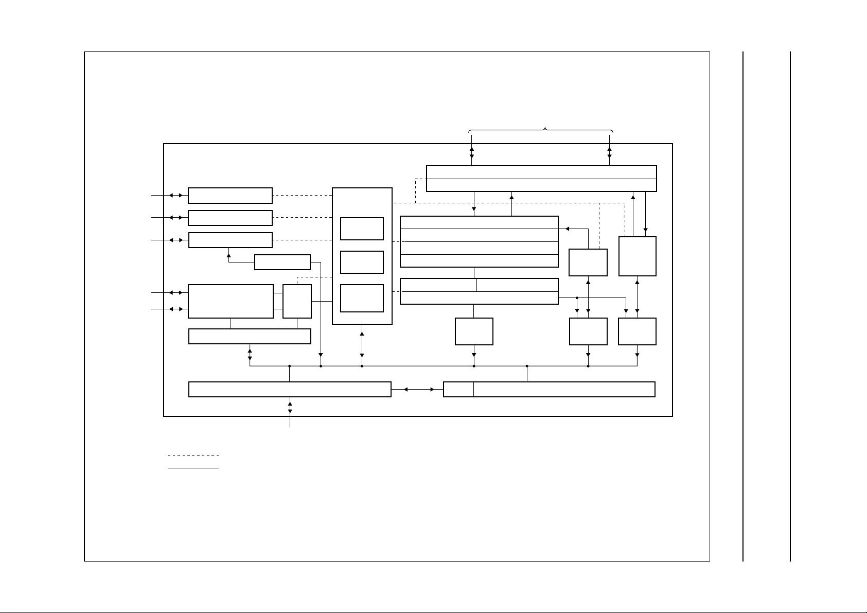
Figure 1 shows the various interface ports and the main
internal function blocks.
4 ORDERING INFORMATION
PACKAGE
TYPE NUMBER
NAME DESCRIPTION VERSION
SAA7146AH QFP160 plastic quad flat package; 160 leads (lead length 1.95 mm);
body 28 × 28 × 3.4 mm; high stand-off height
SAA7146AHZ SQFP208 plastic shrink quad flat package; 208 leads (lead length 1.3 mm);
body 28 × 28 × 3.4 mm
SOT322-1
SOT316-1
1998 Apr 09 4
Page 5
This text is here in white to force landscape pages to be rotated correctly when browsing through the pdf in the Acrobat reader.This text is here in
o
_white to force landscape pages to be rotated correctly when browsing through the pdf in the Acrobat reader.This text is here inThis text is here in
white to force landscape pages to be rotated correctly when browsing through the pdf in the Acrobat reader. white to force landscape pages to be ...
1998 Apr 09 5
k, full pagewidth
Dual D1 or 16-bit YUV
5 BLOCK DIAGRAM
Multimedia bridge, high performance
Scaler and PCI circuit (SPCI)
Philips Semiconductors Product specification
2
C-bus
I
Intel/
Motorola
2
S1-bus
I
2
S2-bus
I
GPIO PORTI/O
I2C-BUS MASTER
DEBI PORT
AUDIO INPUT/OUTPUT
AUDIO INPUT/OUTPUT
AUDIO FIFO
PCI INTERFACE
control
data
SAA7146A
DEBI FIFO
TSL
PCI BUS
RPS
TASK 1
TASK 2
EVENT
MANAGER
REAL TIME VIDEO INTERFACE
8-BIT D1 INPUT/OUTPUT 8-BIT D1 INPUT/OUTPUT
16-BIT YUV IN
YUV
HIGH PERFORMANCE SCALER
H-FILTER/SCALER
V-FILTER/SCALER
VIDEO-FLIP/MIRROR
COLOUR SPACE CV. GAMMA CORRECTION
PIXEL-FORMATTER/DITHER
YUV/RGB
VIDEO
FIFO1
DMA AND INTERNAL ARBITRATION CONTROLLERMMU
CLIPPING
UNIT
VIDEO
FIFO2
YUV
BINARY
RATIO
SCALER
YUV
VIDEO
FIFO3
MHB044
SAA7146A
Fig.1 Block diagram.
Page 6

Philips Semiconductors Product specification
Multimedia bridge, high performance
SAA7146A
Scaler and PCI circuit (SPCI)
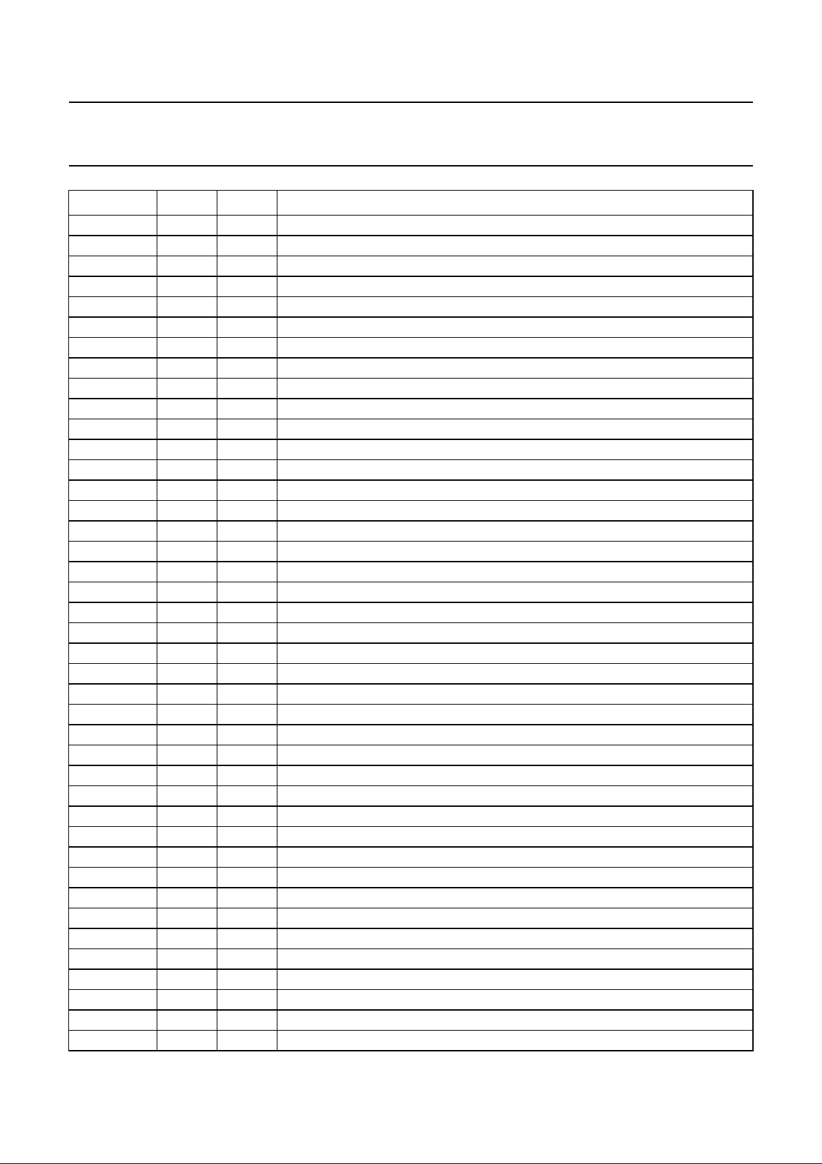
6 PINNING Pin description for QFP160
SYMBOL PIN STATUS DESCRIPTION
D1_A0 1 I/O bidirectional digital CCIR 656 D1 port A bit 0
D1_A1 2 I/O bidirectional digital CCIR 656 D1 port A bit 1
D1_A2 3 I/O bidirectional digital CCIR 656 D1 port A bit 2
D1_A3 4 I/O bidirectional digital CCIR 656 D1 port A bit 3
V
DDD1
V
SSD1
D1_A4 7 I/O bidirectional digital CCIR 656 D1 port A bit 4
D1_A5 8 I/O bidirectional digital CCIR 656 D1 port A bit 5
D1_A6 9 I/O bidirectional digital CCIR 656 D1 port A bit 6
D1_A7 10 I/O bidirectional digital CCIR 656 D1 port A bit 7
VS_A 11 I/O bidirectional vertical sync signal port A
HS_A 12 I/O bidirectional horizontal sync signal port A
LLC_A 13 I/O bidirectional line-locked system clock port A
PXQ_A 14 I/O bidirectional pixel qualifier signal to mark valid pixels port A; note 1
V
DDD2
V
SSD2
TRST 17 I test reset input (JTAG pin must be set LOW for normal operation)
TMS 18 I test mode select input (JTAG pin must be floating or set to HIGH during normal
TCLK 19 I test clock input (JTAG pin should be set LOW during normal operation)
TDO 20 O test data output (JTAG pin not active during normal operation)
TDI 21 I test data input (JTAG pin must be floating or set to HIGH during normal operation)
V
DDD3
V
SSD3
INTA# 24 O PCI interrupt line output (active LOW)
RST 25 I PCI global reset input (active LOW)
CLK 26 I PCI clock input
GNT# 27 I bus grant input signal, PCI arbitration signal (active LOW)
REQ# 28 O bus request output signal, PCI arbitration signal (active LOW)
V
DDD4
V
SSD4
AD PCI31 31 I/O bidirectional PCI multiplexed address/data bit 31
AD PCI30 32 I/O bidirectional PCI multiplexed address/data bit 30
AD PCI29 33 I/O bidirectional PCI multiplexed address/data bit 29
AD PCI28 34 I/O bidirectional PCI multiplexed address/data bit 28
V
DDD5
V
SSD5
AD PCI27 37 I/O bidirectional PCI multiplexed address/data bit 27
5 P digital supply voltage 1 (3.3 V)
6 P digital ground 1
15 P digital supply voltage 2 (3.3 V)
16 P digital ground 2
operation)
22 P digital supply voltage 3 (3.3 V)
23 P digital ground 3
29 P digital supply voltage 4 (3.3 V)
30 P digital ground 4
35 P digital supply voltage 5 (3.3 V)
36 P digital ground 5
1998 Apr 09 6
Page 7

Philips Semiconductors Product specification
Multimedia bridge, high performance
SAA7146A
Scaler and PCI circuit (SPCI)
SYMBOL PIN STATUS DESCRIPTION
AD PCI26 38 I/O bidirectional PCI multiplexed address/data bit 26
AD PCI25 39 I/O bidirectional PCI multiplexed address/data bit 25
AD PCI24 40 I/O bidirectional PCI multiplexed address/data bit 24
C/BE# [3] 41 I/O bidirectional PCI multiplexed bus command and byte enable 3 (active LOW)
IDSEL 42 I PCI initialization device select signal input
AD PCI23 43 I/O bidirectional PCI multiplexed address/data bit 23
AD PCI22 44 I/O bidirectional PCI multiplexed address/data bit 22
AD PCI21 45 I/O bidirectional PCI multiplexed address/data bit 21
AD PCI20 46 I/O bidirectional PCI multiplexed address/data bit 20
V
DDD6
V
SSD6
AD PCI19 49 I/O bidirectional PCI multiplexed address/data bit 19
AD PCI18 50 I/O bidirectional PCI multiplexed address/data bit 18
AD PCI17 51 I/O bidirectional PCI multiplexed address/data bit 17
AD PCI16 52 I/O bidirectional PCI multiplexed address/data bit 16
V
DDD7
V
SSD7
C/BE# [2] 55 I/O bidirectional PCI multiplexed bus command and byte enable 2 (active LOW)
FRAME# 56 I/O bidirectional PCI cycle frame signal (active LOW)
IRDY# 57 I/O bidirectional PCI initiator ready signal (active LOW)
TRDY# 58 I/O bidirectional PCI target ready signal (active LOW)
DEVSEL# 59 I/O bidirectional PCI device select signal (active LOW)
STOP# 60 I/O bidirectional PCI stop signal (active LOW)
PERR# 61 O PCI parity error signal output (active LOW)
PAR 62 I/O bidirectional PCI parity signal
C/BE# [1] 63 I/O bidirectional PCI-bus command and byte enable 1 (active LOW)
V
DDD8
V
SSD8
AD PCI15 66 I/O bidirectional PCI multiplexed address/data bit 15
AD PCI14 67 I/O bidirectional PCI multiplexed address/data bit 14
AD PCI13 68 I/O bidirectional PCI multiplexed address/data bit 13
AD PCI12 69 I/O bidirectional PCI multiplexed address/data bit 12
V
DDD9
V
SSD9
AD PCI11 72 I/O bidirectional PCI multiplexed address/data bit 11
AD PCI10 73 I/O bidirectional PCI multiplexed address/data bit 10
AD PCI9 74 I/O bidirectional PCI multiplexed address/data bit 9
AD PCI8 75 I/O bidirectional PCI multiplexed address/data bit 8
V
DDD10
V
SSD10
C/BE# [0] 78 I/O bidirectional PCI multiplexed bus command and byte enable 0 (active LOW)
47 P digital supply voltage 6 (3.3 V)
48 P digital ground 6
53 P digital supply voltage 7 (3.3 V)
54 P digital ground 7
64 P digital supply voltage 8 (3.3 V)
65 P digital ground 8
70 P digital supply voltage 9 (3.3 V)
71 P digital ground 9
76 P digital supply voltage 10 (3.3 V)
77 P digital ground 10
1998 Apr 09 7
Page 8

Philips Semiconductors Product specification
Multimedia bridge, high performance
SAA7146A
Scaler and PCI circuit (SPCI)
SYMBOL PIN STATUS DESCRIPTION
AD PCI7 79 I/O bidirectional PCI multiplexed address/data bit 7
AD PCI6 80 I/O bidirectional PCI multiplexed address/data bit 6
V
SSD11
AD PCI5 82 I/O bidirectional PCI multiplexed address/data bit 5
AD PCI4 83 I/O bidirectional PCI multiplexed address/data bit 4
AD PCI3 84 I/O bidirectional PCI multiplexed address/data bit 3
AD PCI2 85 I/O bidirectional PCI multiplexed address/data bit 2
V
DDD11
V
SSD12
AD PCI1 88 I/O bidirectional PCI multiplexed address/data bit 1
AD PCI0 89 I/O bidirectional PCI multiplexed address/data bit 0
V
DDD12
V
SSD13
AD15 92 I/O bidirectional DEBI multiplexed address data line bit 15
AD14 93 I/O bidirectional DEBI multiplexed address data line bit 14
AD13 94 I/O bidirectional DEBI multiplexed address data line bit 13
AD12 95 I/O bidirectional DEBI multiplexed address data line bit 12
V
DDD13
V
SSD14
AD11 98 I/O bidirectional DEBI multiplexed address data line bit 11
AD10 99 I/O bidirectional DEBI multiplexed address data line bit 10
AD9 100 I/O bidirectional DEBI multiplexed address data line bit 9
AD8 101 I/O bidirectional DEBI multiplexed address data line bit 8
V
DDD14
V
SSD15
RWN_SBHE 104 O DEBI data transfer control signal output (read write not/system byte high enable)
AS_ALE 105 O DEBI address strobe and address latch enable output
LDS_RDN 106 O lower data strobe/read not output
UDS_WRN 107 O upper data strobe/write not output
DTACK_RDY 108 I DEBI data transfer acknowledge or ready input
V
DDD15
V
SSD16
AD0 111 I/O bidirectional DEBI multiplexed address data line bit 0
AD1 112 I/O bidirectional DEBI multiplexed address data line bit 1
AD2 113 I/O bidirectional DEBI multiplexed address data line bit 2
AD3 114 I/O bidirectional DEBI multiplexed address data line bit 3
V
DDD16
V
SSD17
AD4 117 I/O bidirectional DEBI multiplexed address data line bit 4
AD5 118 I/O bidirectional DEBI multiplexed address data line bit 5
81 P digital ground 11
86 P digital supply voltage 11 (3.3 V)
87 P digital ground 12
90 P digital supply voltage 12 (3.3 V)
91 P digital ground 13
96 P digital supply voltage 13 (3.3 V)
97 P digital ground 14
102 P digital supply voltage 14 (3.3 V)
103 P digital ground 15
109 P digital supply voltage 15 (3.3 V)
110 P digital ground 16
115 P digital supply voltage 16 (3.3 V)
116 P digital ground 17
1998 Apr 09 8
Page 9

Philips Semiconductors Product specification
Multimedia bridge, high performance
Scaler and PCI circuit (SPCI)
SYMBOL PIN STATUS DESCRIPTION
AD6 119 I/O bidirectional DEBI multiplexed address data line bit 6
AD7 120 I/O bidirectional DEBI multiplexed address data line bit 7
WS0 121 I/O bidirectional word select signal for audio interface A1
SD0 122 I/O bidirectional serial data for audio interface A1
BCLK1 123 I/O bidirectional bit clock for audio interface A1
WS1 124 O word select output signal for audio interface A1/A2
SD1 125 I/O bidirectional serial data for audio interface A1/A2
WS2 126 O word select output signal for audio interface A1/A2
SD2 127 I/O bidirectional serial data for audio interface A1/A2
V
DDD17
V
SSD18
WS3 130 O word select output signal for audio interface A1/A2
SD3 131 I/O bidirectional serial data for audio interface A1/A2
BCLK2 132 I/O bidirectional bit clock for audio interface A2
WS4 133 I/O bidirectional word select signal for audio interface A2
SD4 134 I/O bidirectional serial data for audio interface A2
ACLK 135 I audio reference clock input signal
SCL 136 I/O bidirectional I
SDA 137 I/O bidirectional I
V
DDD18
V
DDI2C
V
SSD19
GPIO3 141 I/O general purpose I/O signal 3
GPIO2 142 I/O general purpose I/O signal 2
GPIO1 143 I/O general purpose I/O signal 1
GPIO0 144 I/O general purpose I/O signal 0
D1_B0 145 I/O bidirectional digital CCIR 656 D1 port B bit 0
D1_B1 146 I/O bidirectional digital CCIR 656 D1 port B bit 1
D1_B2 147 I/O bidirectional digital CCIR 656 D1 port B bit 2
D1_B3 148 I/O bidirectional digital CCIR 656 D1 port B bit 3
V
DDD19
V
SSD20
D1_B4 151 I/O bidirectional digital CCIR 656 D1 port B bit 4
D1_B5 152 I/O bidirectional digital CCIR 656 D1 port B bit 5
D1_B6 153 I/O bidirectional digital CCIR 656 D1 port B bit 6
D1_B7 154 I/O bidirectional digital CCIR 656 D1 port B bit 7
V
DDD20
V
SSD21
LLC_B 157 I/O bidirectional line-locked system clock port B
VS_B 158 I/O bidirectional vertical sync signal port B
128 P digital supply voltage 17 (3.3 V)
129 P digital ground 18
2
C-bus clock line
2
C-bus data line
138 P digital supply voltage 18 (3.3 V)
139 I I2C-bus voltage sense input; see note 3 of “Characteristics”
140 P digital ground 19
149 P digital supply voltage 19 (3.3 V)
150 P digital ground 20
155 P digital supply voltage 20 (3.3 V)
156 P digital ground 21
SAA7146A
1998 Apr 09 9
Page 10
Philips Semiconductors Product specification
Multimedia bridge, high performance
SAA7146A
Scaler and PCI circuit (SPCI)
SYMBOL PIN STATUS DESCRIPTION
HS_B 159 I/O bidirectional horizontal sync signal port B
PXQ_B 160 I/O bidirectional pixel qualifier signal to mark valid pixels port B; note 2
Notes
1. For continuous CCIR 656 format at the D1_A port this pin must be set HIGH.
2. For continuous CCIR 656 format at the D1_B port this pin must be set HIGH.
handbook, halfpage
160
1
121
120
SAA7146AH
40
41
80
81
MHB045
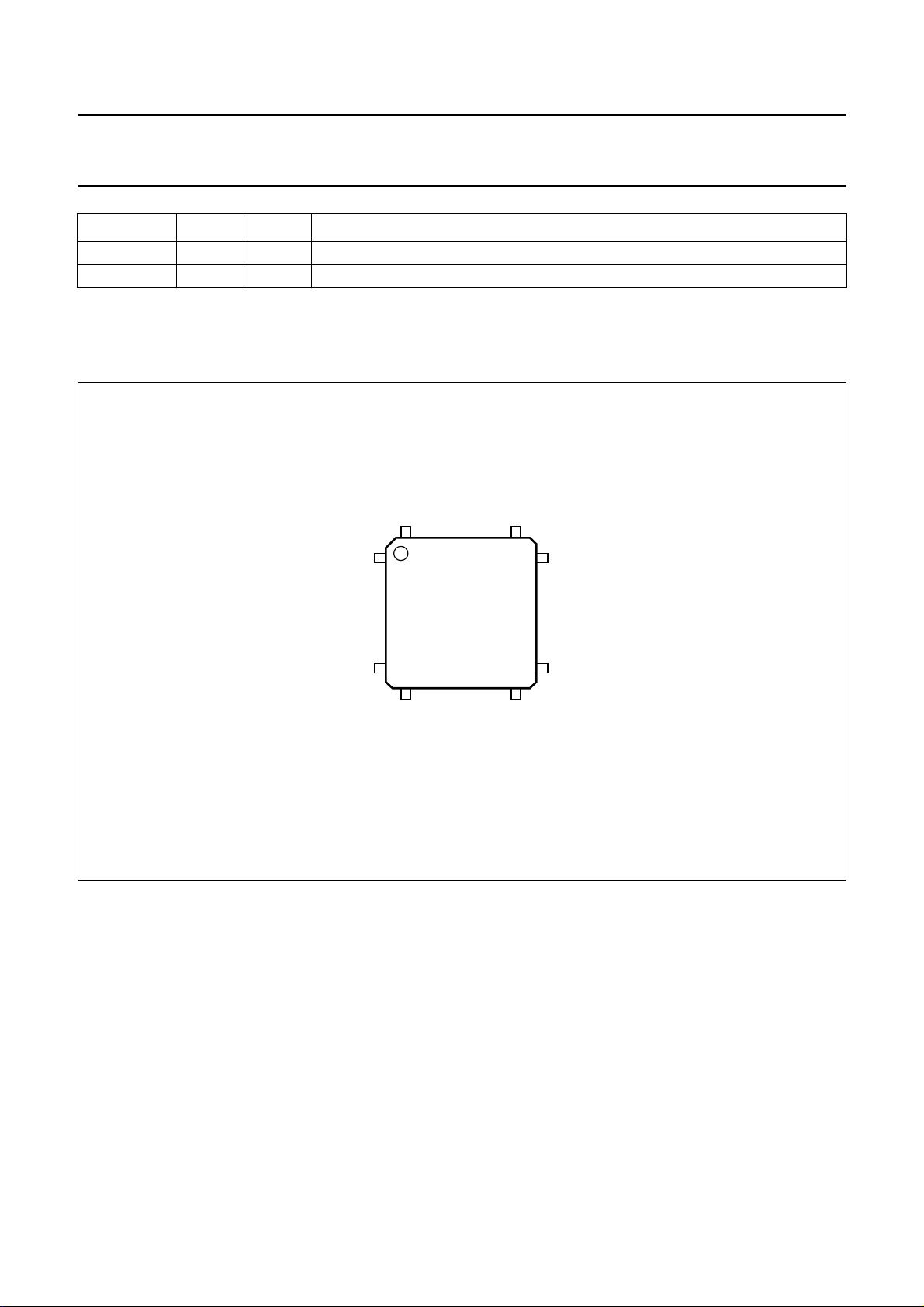
Fig.2 Pin configuration SAA7146AH (QFP160).
1998 Apr 09 10
Page 11

Philips Semiconductors Product specification
Multimedia bridge, high performance
SAA7146A
Scaler and PCI circuit (SPCI)
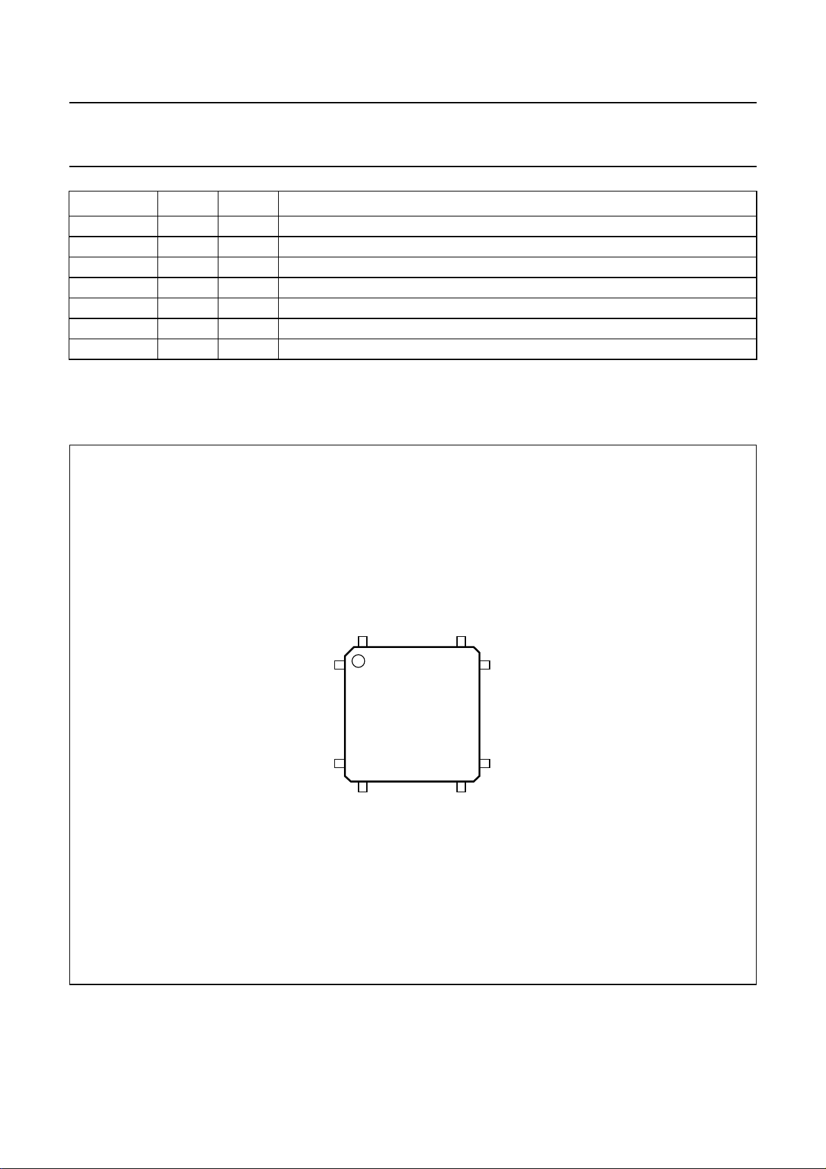
Pin description for SQFP208
SYMBOL PIN STATUS DESCRIPTION
V
SSD0
D1_A0 2 I/O bidirectional digital CCIR 656 D1 port A bit 0
D1_A1 3 I/O bidirectional digital CCIR 656 D1 port A bit 1
D1_A2 4 I/O bidirectional digital CCIR 656 D1 port A bit 2
D1_A3 5 I/O bidirectional digital CCIR 656 D1 port A bit 3
V
DDD1
n.c. 7 − reserved pin; not connected internally
V
SSD1
D1_A4 9 I/O bidirectional digital CCIR 656 D1 port A bit 4
D1_A5 10 I/O bidirectional digital CCIR 656 D1 port A bit 5
D1_A6 11 I/O bidirectional digital CCIR 656 D1 port A bit 6
D1_A7 12 I/O bidirectional digital CCIR 656 D1 port A bit 7
V
DDD2
n.c. 14 − reserved pin; not connected internally
V
SSD2
VS_A 16 I/O bidirectional vertical sync signal port A
HS_A 17 I/O bidirectional horizontal sync signal port A
LLC_A 18 I/O bidirectional line-locked system clock port A
PXQ_A 19 I/O bidirectional pixel qualifier signal to mark valid pixels port A; note 1
n.c. 20 − reserved pin; do not connect
V
DDD3
n.c. 22 − reserved pin; not connected internally
V
SSD3
TRST 24 I test reset input (JTAG pin must be set LOW for normal operation)
TMS 25 I test mode select input (JTAG pin must be floating or set to HIGH during normal
TCLK 26 I test clock input (JTAG pin should be set LOW during normal operation)
TDO 27 O test data output (JTAG pin not active during normal operation)
TDI 28 I test data input (JTAG pin must be floating or set to HIGH during normal operation)
V
DDD4
n.c. 30 − reserved pin; not connected internally
V
SSD4
INTA# 32 O PCI interrupt line output (active LOW)
RST# 33 I PCI global reset input (active LOW)
CLK 34 I PCI clock input
GNT# 35 I bus grant input signal input, PCI arbitration signal (active LOW)
REQ# 36 O bus request output signal output, PCI arbitration signal (active LOW)
V
DDD5
n.c. 38 − reserved pin; not connected internally
1 P digital ground 0
6 P digital supply voltage 1 (3.3 V)
8 P digital ground 1
13 P digital supply voltage 2 (3.3 V)
15 P digital ground 2
21 P digital supply voltage 3 (3.3 V)
23 P digital ground 3
operation)
29 P digital supply voltage 4 (3.3 V)
31 P digital ground 4
37 P digital supply voltage 5 (3.3 V)
1998 Apr 09 11
Page 12

Philips Semiconductors Product specification
Multimedia bridge, high performance
SAA7146A
Scaler and PCI circuit (SPCI)
SYMBOL PIN STATUS DESCRIPTION
V
SSD5
AD PCI31 40 I/O bidirectional PCI multiplexed address/data bit 31
AD PCI30 41 I/O bidirectional PCI multiplexed address/data bit 30
AD PCI29 42 I/O bidirectional PCI multiplexed address/data bit 29
AD PCI28 43 I/O bidirectional PCI multiplexed address/data bit 28
V
DDD6
n.c. 45 − reserved pin; not connected internally
V
SSD6
AD PCI27 47 I/O bidirectional PCI multiplexed address/data bit 27
AD PCI26 48 I/O bidirectional PCI multiplexed address/data bit 26
AD PCI25 49 I/O bidirectional PCI multiplexed address/data bit 25
AD PCI24 50 I/O bidirectional PCI multiplexed address/data bit 24
V
DDD7
n.c. 52 − reserved pin; do not connect
n.c. 53 − reserved pin; not connected internally
V
SSD7
C/BE# [3] 55 I/O bidirectional PCI multiplexed bus command and byte enable 3 (active LOW)
IDSEL 56 I PCI initialization device select input signal
AD PCI23 57 I/O bidirectional PCI multiplexed address/data bit 23
AD PCI22 58 I/O bidirectional PCI multiplexed address/data bit 22
AD PCI21 59 I/O bidirectional PCI multiplexed address/data bit 21
AD PCI20 60 I/O bidirectional PCI multiplexed address/data bit 20
n.c. 61 − reserved pin; do not connect
n.c. 62 − reserved pin; not connected internally
V
SSD8
AD PCI19 64 I/O bidirectional PCI multiplexed address/data bit 19
AD PCI18 65 I/O bidirectional PCI multiplexed address/data bit 18
AD PCI17 66 I/O bidirectional PCI multiplexed address/data bit 17
AD PCI16 67 I/O bidirectional PCI multiplexed address/data bit 16
V
DDD8
n.c. 69 − reserved pin; do not connect
V
SSD9
C/BE# [2] 71 I/O bidirectional PCI multiplexed bus command and byte enable 2 (active LOW)
FRAME# 72 I/O bidirectional PCI cycle frame signal (active LOW)
IRDY# 73 I/O bidirectional PCI initiator ready signal (active LOW)
TRDY# 74 I/O bidirectional PCI target ready signal (active LOW)
V
DDD9
n.c. 76 − reserved pin; do not connect
V
SSD10
DEVSEL# 78 I/O bidirectional PCI device select signal (active LOW)
39 P digital ground 5
44 P digital supply voltage 6 (3.3 V)
46 P digital ground 6
51 P digital supply voltage 7 (3.3 V)
54 P digital ground 7
63 P digital ground 8
68 P digital supply voltage 8 (3.3 V)
70 P digital ground 9
75 P digital supply voltage 9 (3.3 V)
77 P digital ground 10
1998 Apr 09 12
Page 13

Philips Semiconductors Product specification
Multimedia bridge, high performance
SAA7146A
Scaler and PCI circuit (SPCI)
SYMBOL PIN STATUS DESCRIPTION
STOP# 79 I/O bidirectional PCI stop signal (active LOW)
PERR# 80 O PCI parity error output signal (active LOW)
n.c. 81 − reserved pin; do not connect
PAR 82 I/O bidirectional PCI parity signal
C/BE# [1] 83 I/O bidirectional PCI-bus command and byte enable 1 (active LOW)
V
DDD10
n.c. 85 − reserved pin; not connected internally
V
SSD11
AD PCI15 87 I/O bidirectional PCI multiplexed address/data bit 15
AD PCI14 88 I/O bidirectional PCI multiplexed address/data bit 14
AD PCI13 89 I/O bidirectional PCI multiplexed address/data bit 13
AD PCI12 90 I/O bidirectional PCI multiplexed address/data bit 12
V
DDD11
n.c. 92 − reserved pin; not connected internally
V
SSD12
AD PCI11 94 I/O bidirectional PCI multiplexed address/data bit 11
AD PCI10 95 I/O bidirectional PCI multiplexed address/data bit 10
AD PCI9 96 I/O bidirectional PCI multiplexed address/data bit 9
AD PCI8 97 I/O bidirectional PCI multiplexed address/data bit 8
n.c. 98 − reserved pin; do not connect
n.c. 99 − reserved pin; not connected internally
V
SSD13
C/BE# [0] 101 I/O bidirectional PCI multiplexed bus command and byte enable (active LOW)
AD PCI7 102 I/O bidirectional PCI multiplexed address/data bit 7
AD PCI6 103 I/O bidirectional PCI multiplexed address/data bit 6
V
DDD12
n.c. 105 − reserved pin; do not connect
n.c. 106 − reserved pin; not connected internally
V
SSD14
AD PCI5 108 I/O bidirectional PCI multiplexed address/data bit 5
AD PCI4 109 I/O bidirectional PCI multiplexed address/data bit 4
AD PCI3 110 I/O bidirectional PCI multiplexed address/data bit 3
AD PCI2 111 I/O bidirectional PCI multiplexed address/data bit 2
V
DDD13
n.c. 113 − reserved pin; not connected internally
V
SSD15
AD PCI1 115 I/O bidirectional PCI multiplexed address/data bit 1
AD PCI0 116 I/O bidirectional PCI multiplexed address/data bit 0
V
DDD14
n.c. 118 − reserved pin; not connected internally
V
SSD16
84 P digital supply voltage 10 (3.3 V)
86 P digital ground 11
91 P digital supply voltage 11 (3.3 V)
93 P digital ground 12
100 P digital ground 13
104 P digital supply voltage 12 (3.3 V)
107 P digital ground 14
112 P digital supply voltage 13 (3.3 V)
114 P digital ground 15
117 P digital supply voltage 14 (3.3 V)
119 P digital ground 16
1998 Apr 09 13
Page 14
Philips Semiconductors Product specification
Multimedia bridge, high performance
SAA7146A
Scaler and PCI circuit (SPCI)
SYMBOL PIN STATUS DESCRIPTION
AD15 120 I/O bidirectional DEBI multiplexed address data line bit 15
AD14 121 I/O bidirectional DEBI multiplexed address data line bit 14
AD13 122 I/O bidirectional DEBI multiplexed address data line bit 13
AD12 123 I/O bidirectional DEBI multiplexed address data line bit 12
V
DDD15
n.c. 125 − reserved pin; not connected internally
V
SSD17
AD11 127 I/O bidirectional DEBI multiplexed address data line bit 11
AD10 128 I/O bidirectional DEBI multiplexed address data line bit 10
AD9 129 I/O bidirectional DEBI multiplexed address data line bit 9
AD8 130 I/O bidirectional DEBI multiplexed address data line bit 8
V
DDD16
n.c. 132 − reserved pin; not connected internally
V
SSD18
RWN_SBHE 134 O DEBI data transfer control output signal (read write not/system byte high enable)
AS_ALE 135 O DEBI address strobe and address latch enable output
LDS_RDN 136 O lower data strobe/read not output
UDS_WRN 137 O upper data strobe/write not output
DTACK_RDY 138 I DEBI data transfer acknowledge or ready input
V
DDD17
n.c. 140 − reserved pin; not connected internally
V
SSD19
AD0 142 I/O bidirectional DEBI multiplexed address data line bit 0
AD1 143 I/O bidirectional DEBI multiplexed address data line bit 1
AD2 144 I/O bidirectional DEBI multiplexed address data line bit 2
AD3 145 I/O bidirectional DEBI multiplexed address data line bit 3
V
DDD18
n.c. 147 − reserved pin; not connected internally
V
SSD20
AD4 149 I/O bidirectional DEBI multiplexed address data line bit 4
AD5 150 I/O bidirectional DEBI multiplexed address data line bit 5
AD6 151 I/O bidirectional DEBI multiplexed address data line bit 6
AD7 152 I/O bidirectional DEBI multiplexed address data line bit 7
n.c. 153 − reserved pin; do not connect
n.c. 154 − reserved pin; do not connect
V
DDD19
n.c. 156 − reserved pin; not connected internally
n.c. 157 − reserved pin; do not connect
V
SSD21
WS0 159 I/O bidirectional word select signal for audio interface A1
SD0 160 I/O bidirectional serial data for audio interface A1
124 P digital supply voltage 15 (3.3 V)
126 P digital ground 17
131 P digital supply voltage 16 (3.3 V)
133 P digital ground 18
139 P digital supply voltage 17 (3.3 V)
141 P digital ground 19
146 P digital supply voltage 18 (3.3 V)
148 P digital ground 20
155 P digital supply voltage 19 (3.3 V)
158 P digital ground 21
1998 Apr 09 14
Page 15
Philips Semiconductors Product specification
Multimedia bridge, high performance
Scaler and PCI circuit (SPCI)
SYMBOL PIN STATUS DESCRIPTION
BCLK1 161 I/O bidirectional bit clock for audio interface A1
WS1 162 O word select output signal for audio interface A1/A2
SD1 163 I/O bidirectional serial data for audio interface A1/A2
WS2 164 O word select output signal for audio interface A1/A2
SD2 165 I/O bidirectional serial data for audio interface A1/A2
V
DDD20
n.c. 167 − reserved pin; not connected internally
V
SSD22
WS3 169 O word select output signal for audio interface A1/A2
SD3 170 I/O bidirectional serial data for audio interface A1/A2
BCLK2 171 I/O bidirectional bit clock for audio interface A2
WS4 172 I/O bidirectional word select signal for audio interface A2
SD4 173 I/O bidirectional serial data for audio interface A2
ACLK 174 I audio reference clock input signal
SCL 175 I/O bidirectional I
SDA 176 I/O bidirectional I
V
DDD21
V
DDI2C
V
SSD23
GPIO3 180 I/O general purpose I/O signal 3
GPIO2 181 I/O general purpose I/O signal 2
GPIO1 182 I/O general purpose I/O signal 1
GPIO0 183 I/O general purpose I/O signal 0
V
DDD22
n.c. 185 − reserved pin; not connected internally
V
SSD24
D1_B0 187 I/O bidirectional digital CCIR 656 D1 port B bit 0
D1_B1 188 I/O bidirectional digital CCIR 656 D1 port B bit 1
D1_B2 189 I/O bidirectional digital CCIR 656 D1 port B bit 2
D1_B3 190 I/O bidirectional digital CCIR 656 D1 port B bit 3
V
DDD23
n.c. 192 − reserved pin; not connected internally
V
SSD25
D1_B4 194 I/O bidirectional digital CCIR 656 D1 port B bit 4
D1_B5 195 I/O bidirectional digital CCIR 656 D1 port B bit 5
D1_B6 196 I/O bidirectional digital CCIR 656 D1 port B bit 6
D1_B7 197 I/O bidirectional digital CCIR 656 D1 port B bit 7
V
DDD24
n.c. 199 − reserved pin; not connected internally
V
SSD26
LLC_B 201 I/O bidirectional line-locked system clock port B
166 P digital supply voltage 20 (3.3 V)
168 P digital ground 22
2
C-bus clock line
2
C-bus data line
177 P digital supply voltage 21 (3.3 V)
178 I I2C-bus voltage sense input; see note 3 of “Characteristics”
179 P digital ground 23
184 P digital supply voltage 22 (3.3 V)
186 P digital ground 24
191 P digital supply voltage 23 (3.3 V)
193 P digital ground 25
198 P digital supply voltage 24 (3.3 V)
200 P digital ground 26
SAA7146A
1998 Apr 09 15
Page 16
Philips Semiconductors Product specification
Multimedia bridge, high performance
SAA7146A
Scaler and PCI circuit (SPCI)
SYMBOL PIN STATUS DESCRIPTION
VS_B 202 I/O bidirectional vertical sync signal port B
HS_B 203 I/O bidirectional horizontal sync signal port B
PXQ_B 204 I/O bidirectional pixel qualifier signal to mark valid pixels port B; note 2
n.c. 205 − reserved pin; do not connect
V
DDD25
n.c. 207 − reserved pin; not connected internally
n.c. 208 − reserved pin; do not connect
Notes
1. For continuous CCIR 656 format at the D1_A port this pin must be set HIGH.
2. For continuous CCIR 656 format at the D1_B port this pin must be set HIGH.
206 P digital supply voltage 25 (3.3 V)
handbook, halfpage
52
208
1
SAA7146AHZ
53
157
104
156
105
MHB046
Fig.3 Pin configuration SAA7146AHZ (SQFP208).
1998 Apr 09 16
Page 17

Philips Semiconductors Product specification
Multimedia bridge, high performance
Scaler and PCI circuit (SPCI)
7 FUNCTIONAL DESCRIPTION
This chapter provides information about the features
realized with this device. First, a general, thus short,
description of the functionality is given. The following
sections deal with the single features in a detailed manner.
7.1 General
The Dual D1 (DD1) interface can be connected to digital
video decoder ICs such as the SAA7110 and SAA7111A,
digital video encoder such as the SAA7185B, video
compression CODECs or to a D1 compatible connector,
e.g. for interconnection to an external digital camera.
The interface supports bidirectional full duplex two channel
full D1 (CCIR 656), optionally with separate sync lines
H/V, pixel qualifier signal and double pixel clock I/O, up to
32 MHz. It also supports a 16-bit parallel ‘YUV bus’ for
interfacing to the SAA7110.
One of the two internal video processors of the SAA7146A
is the two-dimensional High Performance Scaler (HPS).
Phase accurate re-sampling by interpolation supports
independent horizontal up and downscaling. In the
horizontal direction the scaling process is performed in two
functional blocks: integer decimation by window averaging
(up to 65 tap), and phase linear interpolation (10 tap filter
for luminance, 6 tap filter for chrominance). The vertical
processing for downscaling either uses averaging over a
window (up to 65 tap) or linear interpolation (2 tap).
The scaling function can be used for random sized display
windowing, for horizontal upscaling (zoom) or for
conversion between various sample schemes such as
CCIR or SQP. Incorporated with the HPS function is
brightness, contrast and saturation control. Colour key
generation is also established. The output of the HPS can
be formatted in various RGB and YUV formats.
Additionally, this output can be dithered for low bit rate
formats. Packed formats as well as planar formats (YUV)
are supported.
A second video channel (YUV4:2:2 format) bypasses
the HPS and connects the real time video interface with
the PCI interface. This video bypass channel, using the
second video processor Binary Ratio Scaler (BRS), is
bidirectional and has means to convert from full size video
(50 or 60 Hz) to Common Interchange Format (CIF),
Quarter Common Interchange Format (QCIF) or Quarter
Quarter Common Interchange Format (QQCIF) and vice
versa (binary ratio 1, 2, 4, 8,
programmable VBI data and test signal regions can be
bypassed without processing during each field.
1
⁄2,1⁄4and1⁄8only). Multiple
SAA7146A
The bidirectional digital audio serial interface is based on
2
the I
S-bus standard, but supports flexible programming
for various data and timing formats.
Two independent interface circuits control audio data
streaming of up to 2 × 128-bit frame width (bidirectional or
simultaneous input/output). Five or more I2S devices such
as the SAA7360 and SAA7366 (ADC) and SAA7350 and
SAA7351 (DAC) can be connected gluelessly.
The peripheral data port [Data Expansion Bus Interface
(DEBI)] enables 8 or 16-bit parallel access for system
set-up and programming of peripheral multimedia devices
(behind SAA7146A), but is also highly capable to interface
compressed MPEG/JPEG data of peripheral ICs with the
PCI system. DEBI supports both Intel compatible (ISA-bus
like) and Motorola (68000 style) compatible handshaking
protocols with up to 23 Mbytes/s peak data rate. Besides
the parallel port, there is also an I2C-bus port to control
peripheral ICs such as single-chip decoders SAA7110 and
SAA7111A or as encoders such as SAA7185B and
SAA7187 or as audio ICs.
The PCI interface has master read and master write
capability. The video signal flows to and from the PCI and
is controlled by three video DMA channels with a total
FIFO capacity of 384 Dwords. The video DMA channel
definition supports the typical video data structure
(hierarchy) of pixels, lines, fields and frames. The audio
signal flow is controlled by four audio DMA channels, each
with 24 Dwords FIFO capacity. The DEBI port is
connected to the PCI by single instruction direct access
(immediate mode) and via a data DMA channel for
streaming data (block mode) with 32 Dwords FIFO
capacity. To improve PCI-bus efficiency, an arbiter
schedules the access to PCI-bus for all local DMA
channels.
The PCI interface of the SAA7146A supports virtual
memory addressing for operating systems running virtual
demand paging. The integrated Memory Management
Unit (MMU) translates linear addressing to physical
addresses using a page table inside the system memory
provided by the software driver. The MMU supports up to
4 Mbytes of virtual address space per DMA channel.
The SAA7146A can change its programming sets using a
Register Programming Sequencer (RPS) that works by
itself on a user defined program controlled by internally
supported real time events. The SAA7146A has two RPS
machines to optimize flow control of e.g. an MPEG
compressed data stream and real time video scaling
control. The RPS programming is defined by an instruction
list in the system main memory that consists of multiple
RPS commands.
1998 Apr 09 17
Page 18

Philips Semiconductors Product specification
Multimedia bridge, high performance
Scaler and PCI circuit (SPCI)
7.2 PCI interface
This section describes the interface of the SAA7146A to
the PCI-bus. This includes the PCI modules, the DMA
controls of the video, audio and data channels, the
Memory Management Unit (MMU) and the Internal
Arbitration Control (INTAC). The handling of the FIFOs
and the corresponding errors are also described and a list
of all DMA control registers is given.
7.2.1 PCI
The SAA7146A provides a PCI-bus interface having both
slave and master capability. The master and the slave
module fulfil the PCI local bus specification revision 2.1.
They decode the C/BE# lines to provide a byte-wise
access and support 32-bit transfers up to a maximum clock
rate of 33 MHz. To increase bus performance, they are
able to handle fast back-to-back transfers.
During normal operation the SAA7146A checks for parity
errors and reports them via the PERR# pin. If an address
parity error is detected the SAA7146A will not respond.
MODULES AND CONFIGURATION SPACE
SAA7146A
Using the SAA7146A as a slave, access is obtained only
to the programmable registers and to its configuration
space. Video, audio and other data of the SAA7146A
reads/writes autonomously via the master interface (see
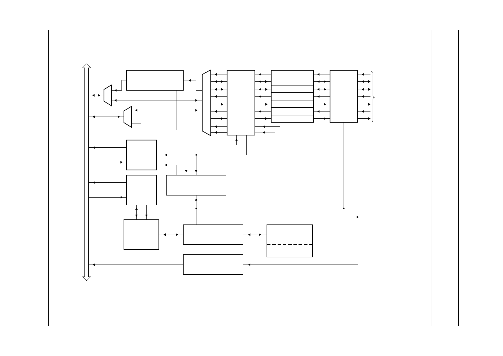
Fig.4). The use of the PCI master module, i.e. which DMA
channel gets access to the PCI-bus, is controlled by the
INTAC (see Section 7.2.5).
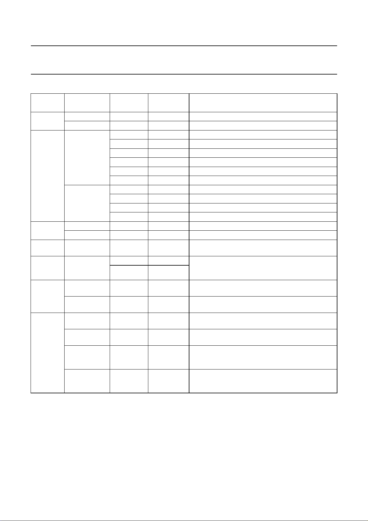
The registers described in Table 1 are closely related to
the PCI specification. It should be noted that Header type,
Cache Line Size, BIST, Card bus CIS Pointer and
Expansion ROM Base Address Registers are not
implemented. All registers, which are not implemented are
treated as read only with a value of zero. Some values are
loaded after PCI reset via I
device address 1010000 (binary). This loading will take
approximately 1 ms at 33 MHz PCI clock. If any device
tries to read or write data from or to the SAA7146A during
the loading phase after reset, the SAA7146A will
disconnect with retry.
2
C-bus from EEPROM with
1998 Apr 09 18
Page 19
This text is here in white to force landscape pages to be rotated correctly when browsing through the pdf in the Acrobat reader.This text is here in
a
_white to force landscape pages to be rotated correctly when browsing through the pdf in the Acrobat reader.This text is here inThis text is here in
white to force landscape pages to be rotated correctly when browsing through the pdf in the Acrobat reader. white to force landscape pages to be ...
1998 Apr 09 19
ndbook, full pagewidth
Philips Semiconductors Product specification
Multimedia bridge, high performance
Scaler and PCI circuit (SPCI)
PCI-bus
physical address
MEMORY MANAGEMENT
data
REGISTER
SHADOW RAM
data
byte enable
bus command
PCI
MODULE
MASTER
PCI
MODULE
SLAVE
AND
UNIT
(MMU)
CE
EOT
new Tr
address
logic
address
channel select
INTERNAL ARBITRA TION
CONTROL
(INTAC)
bus requests
REGISTER PROGRAMMING
SEQUENCER
(RPS)
FIFO
CONTROL
(FICO)
FIFO1
FIFO2
FIFO3
AUDIO FIFO1 OUT
AUDIO FIFO1 IN
AUDIO FIFO2 OUT
AUDIO FIFO2 IN
REGISTER
SETS
2
I
C-BUS REGISTER
FIFO
INPUT
CONTROL
(FINC)
video/audio
data streams
DEBI data/request
ERROR MANAGER
(EMA)
Fig.4 Block diagram of the PCI interface.
interrupts
MHB047
SAA7146A
Page 20
Philips Semiconductors Product specification
Multimedia bridge, high performance
SAA7146A
Scaler and PCI circuit (SPCI)
Table 1 Configuration space registers
ADDRESS
(HEX)
00 Device ID 31 to 16 RO 7146H SAA7146A
04 Status Register 31 − detected parity error
08 Class Code 31 to 8 RO 048000H other multimedia device
0C Latency 15 to 8 RW this register specifies, in units of PCI-bus clocks, the
10 Base Address
2C Subsystem ID 31 to 16 RO this value will be loaded after a PCI reset from external
3C Max_Lat 31 to 24 RO this value will be loaded after a PCI reset from external
NAME BIT TYPE DESCRIPTION
Vendor ID 15 to 0 RO 1131H Philips
29 − received master abort
28 − received target abort
26 and 25 RO 01 DEVSEL# timing medium
24 − data parity error detected
23 RO 1 fast back-to-back capable
Command
Register
Revision ID 7 to 0 RO 01H reading these 8 bits returns 01H
Register
Subsystem
vendor ID
Min_Gnt 23 to 16 RO this value will be loaded after a PCI reset from external
Interrupt Pin 15 to 8 RO 01H The interrupt pin register tells which interrupt pin the
Interrupt Line 7 to 0 RW the interrupt line register tells which input of the system
9 RW fast back-to-back enable
6 RW parity error response
2 RW bus master enable
1 RW memory space
value of the latency timer for this PCI-bus master
31 to 9 RW this value must be added to the register offset to claim
8to0 RO
15 to 0 RO this value will be loaded after a PCI reset from external
access to the programming registers; the lower 8 bits
are forced to zero
hardware using the I
hardware using the I
hardware using the I
hardware using the I
device uses. This device uses interrupt pin INTA#.
When these bits are read they return 01H.
interrupt controller the device’s interrupt pin is
connected to
2
C-bus; the default value is 0000H
2
C-bus; the default value is 0000H
2
C-bus; the default value is 26H
2
C-bus; the default value is 0FH
1998 Apr 09 20
Page 21

Philips Semiconductors Product specification
Multimedia bridge, high performance
Scaler and PCI circuit (SPCI)
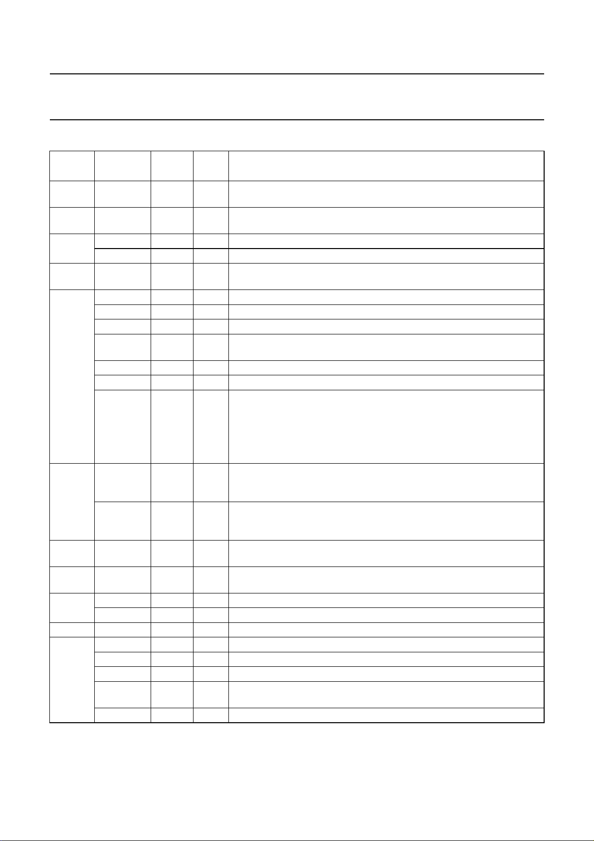
7.2.2 VIDEO DMA CONTROL
The SAA7146A’s DMA control is able to support up to
three independent video targets or sources respectively.
For this purpose it provides three video DMA channels.
Each channel consists of a FIFO, a FIFO Input Control
(FINC) placed on the video side of the FIFO, and a FIFO
Control (FICO) placed on the PCI side of the FIFO.
Channel 1 only supports the unidirectional data stream
into the PCI memory. It is not able to read data from
system memory. However, this access is possible using
Channels 2 or 3. Table 2 surveys the possibilities and
purposes of each video DMA channel.
Each FIFO, i.e. each DMA channel, has its own
programming set including base address (doubled for odd
and even fields), pitch, protection address, page table
base address, several handling mode control bits and a
transfer enable bit (TR_E). In addition, each channel has a
threshold and a burst length definition for internal
arbitration (see Table 6, Section 7.2.5).
SAA7146A
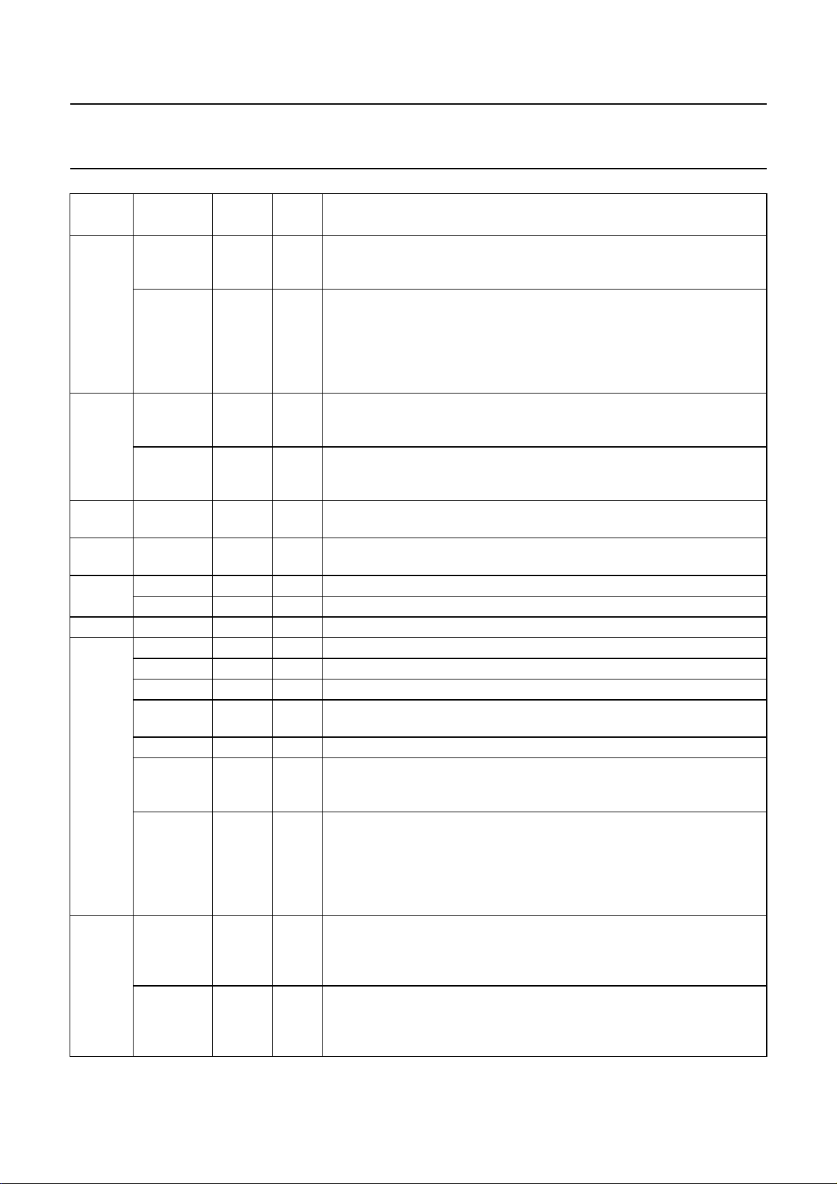
To handle the reading modes FIFO 2 and FIFO 3 offer
some additional registers: Number of Bytes per line
(NumBytes), Number of Lines per field (NumLines) and
the vertical scaling ratio (only FIFO 3, see Table 69).
The programming sets could be reloaded after the
previous job is done [Video Transfer Done (VTD)] to
support several DMA targets per FIFO. The programming
set currently used is loaded by the Register Programming
Sequencer (RPS). If the RPS is not used, the registers
could be rewritten each time, using the SAA7146A as a
slave. But then the programmer must take care of the
synchronization of these write accesses.
All registers needed for DMA control are described in
Table 3, except the transfer enable bits, which are
described in Table 10. The registers are accessed through
PCI base address with appropriate offset (see Table 1).
Table 2 Size, direction and purpose of the video FIFOs and the associated DMA controls
FIFO SIZE DIRECTION PURPOSE
FIFO 1 128 Dwords write to PCI FIFO 1 buffers data from the HPS output and writes into PCI memory.
In planar mode FIFO 1 gets the Y data.
FIFO 2 128 Dwords RW Planar mode: FIFO 2 buffers U data provided by the HPS; the
associated DMA control 2 sends it into the PCI memory.
Clip mode: DMA control 2 reads clipping information (clip bit mask or
rectangular overlay data) from the PCI system memory and buffers it
in FIFO 2.
FIFO 3 128 Dwords RW Planar mode: FIFO 3 buffers V data provided by the HPS and writes
it into the PCI memory.
Chroma keying mode: FIFO 3 buffers chroma keying information
and writes it into PCI memory.
BRS mode: FIFO 3 buffers data provided by the BRS. DMA control 3
sends it into the PCI memory.
Read mode: DMA control 3 reads video data from the PCI system
memory (the same data up to four times to offer a simple upscaling
algorithm) and buffers it in FIFO 3.
1998 Apr 09 21
Page 22
Philips Semiconductors Product specification
Multimedia bridge, high performance
SAA7146A
Scaler and PCI circuit (SPCI)
Table 3 Video DMA control registers
OFFSET
(HEX)
00 BaseOdd1 31 to 0 RW PCI base address for odd fields of the upper (or lower if pitch is
04 BaseEven1 31 to 0 RW PCI base address for even fields of the upper (or lower if pitch is
08 ProtAddr1 31 to 2 RW protection address
0C Pitch1 31 to 0 RW distance between the start addresses of two consecutive lines of a single
10 Page1 31 to 12 RW base address of the page table (see Section 7.2.4)
14 NumLines1 27 to 16 RW Number of lines per field; it defines the number of qualified lines to be
18 BaseOdd2 31 to 0 RW PCI base address for odd fields of the upper (or lower if top-down flip is
1C BaseEven2 31 to 0 RW PCI base address for even fields of the upper (or lower if top-down flip is
20 ProtAddr2 31 to 2 RW protection address
24 Pitch2 31 to 0 RW distance between the start addresses of two consecutive lines of a field
28 Page2 31 to 12 RW base address of the page table (see Section 7.2.4)
NAME BIT TYPE DESCRIPTION
negative) left pixel of the transferred field
negative) left pixel of the transferred field
− 1 and 0 − reserved
field
ME1 11 RW mapping enable; this bit enables the MMU
− 10 to 8 − reserved
Limit1 7 to 4 RW interrupt limit; defines the size of the memory range, that raise an
interrupt, if its boundaries are passed
PV1 3 RW protection violation handling
− 2 − reserved
Swap1 1 and 0 RW endian swapping of all Dwords passing the FIFO 1:
00 = no swap
01 = two bytes swap (3210 to 2301)
10 = four bytes swap (3210 to 0123)
11 = reserved
processed by the HPS per field. This will cut off all the following input lines
at the HPS input.
NumBytes1 11 to 0 RW Number of pixels per line; it defines the number of qualified pixels to be
processed by the HPS per line. This will cut off all the following pixels at
the HPS input.
selected) left pixel of the transferred field
selected) left pixel of the transferred field
− 1 and 0 − reserved
ME2 11 RW mapping enable; this bit enables the MMU
− 10 to 8 − reserved
Limit2 7 to 4 RW interrupt limit; defines the size of the memory range, that raise an
interrupt, if its boundaries are passed
PV2 3 RW protection violation handling
1998 Apr 09 22
Page 23
Philips Semiconductors Product specification
Multimedia bridge, high performance
SAA7146A
Scaler and PCI circuit (SPCI)
OFFSET
(HEX)
28 RW2 2 RW Specifies the data stream direction of FIFO 2. A logic 0 enables a write
2C NumLines2 27 to 16 RW Number of lines per field: in read mode NumLines defines the number of
30 BaseOdd3 31 to 0 RW PCI base address for odd fields of the upper (or lower if top-down flip is
34 BaseEven3 31 to 0 RW PCI base address for even fields of the upper (or lower if top-down flip is
38 ProtAddr3 31 to 2 RW protection address
3C Pitch3 31 to 0 RW distance between the start addresses of two consecutive lines of a field
40 Page3 31 to 12 RW base address of the page table (see Section 7.2.4)
44 NumLines3 27 to 16 RW Number of lines per field: in read mode NumLines defines the number of
NAME BIT TYPE DESCRIPTION
operation to the PCI memory. A logic 1 enables a read operation from the
PCI memory.
Swap2 1 and 0 RW endian swapping of all Dwords passing the FIFO 2:
00 = no swap
01 = two byte swap (3210 to 2301)
10 = four byte swap (3210 to 0123)
11 = reserved
lines to be read from system memory. A logic 0 specifies one line. In write
mode this register is not used.
NumBytes2 11 to 0 RW Number of bytes per line: in read mode this defines the number of bytes
per line to be read from system memory. A logic 0 specifies one byte. In
write mode this register is not used.
selected) left pixel of the transferred field
selected) left pixel of the transferred field
− 1 and 0 − reserved
ME3 11 RW mapping enable; this bit enables the MMU
− 10 to 8 − reserved
Limit3 7 to 4 RW interrupt limit; defines the size of the memory range, that raise an
interrupt, if its boundaries are passed
PV3 3 RW protection violation handling
RW3 2 RW Specifies the data stream direction of FIFO 3. A logic 0 enables a write
operation to the PCI memory. A logic 1 enables a read operation from the
PCI memory.
Swap3 1 and 0 RW endian swapping of all Dwords passing the FIFO 3:
00 = no swap
01 = two byte swap (3210 to 2301)
10 = four byte swap (3210 to 0123)
11 = reserved
lines to be read from system memory. A logic 0 specifies one line. In write
mode it defines the number of qualified lines to be processed by the BRS
per field. This will cut off all the following input-lines at the BRS input.
NumBytes3 11 to 0 RW Number of bytes per line: in read mode this defines the number of bytes
per line to be read from system memory. A logic0 specifies 1 byte. In write
mode it defines the number of qualified bytes to be processed by the BRS
per line. This will cut off all the following bytes at the BRS input.
1998 Apr 09 23
Page 24

Philips Semiconductors Product specification
Multimedia bridge, high performance
Scaler and PCI circuit (SPCI)
The video channels provide 32 bits of data signals and
4 bits of Byte Enable (BE) signals, End-Of-Line (EOL),
End-Of-Window (EOW), Begin-Of-Field (BOF),
Line-Locked Clock (LLC), Odd/Even signal (OE) and a
Valid Data (VD) signal. To start a video data transfer, e.g.
via video DMA Channel 3, this channel must first be
included in the internal arbitration scheme. This is
achieved by setting the corresponding TR_E bit
(see Table 10). If a TR_E bit is not set, the corresponding
FIFO is reset.
In read mode, which is offered by Channels 2 and 3, the
FICO requests a PCI transfer with the next BOF. Data is
provided by the PCI master module. The FICO calculates
the PCI address autonomously, starting with the base
address of the corresponding field. Only the received data
will be filled into the FIFO. FIFO 3 offers the possibility to
read video information from PCI memory, e.g. from the
frame buffer. This could be achieved by using the
NumBytes and the NumLines register, which defines the
size of the source picture, so that the DMA control is able
to synchronize itself to the source frame. FIFO 2 does the
same if reading clip information from memory.
To support the Binary Ratio Scaler (BRS) included in the
SAA7146A, which only provides the possibility of
horizontal upscaling, the DMA control 3 can be applied to
perform line repetition by reading lines up to four times
from PCI memory. This feature is controlled by the vertical
scaling ratio in outbound mode (see Table 66). This ratio
specifies the number of times each line should be read:
00 = only once, 01 = twice, and so on.
In the event of FIFO underflow, i.e. if the BRS or the
clipping unit respectively tries to read data from the FIFO,
even if the DMA control was not able to fill any data until
that moment, the reading unit tries to synchronize itself to
the outgoing data stream as soon as possible. In this way
the reading of invalid data is minimized. If the clipping unit
receives no data, it will disable the associated pixels.
The behaviour of the BRS depends on the selected read
mode which is described in Section 7.10.
In the event of FIFO overflow, i.e. if the scaler tries to
transfer data although the FIFO is full, the FIFO input
control locks the FIFO for the incoming data. During FIFO
overflow the PCI address of the incoming data will be
increased, over writing itself each time, if the scaler
transfers data, which has been clipped, the same
mechanism is used to improve PCI performance.
The SAA7146A is able to handle a negative pitch.
With that, top-down-flip of the transmitted fields or frames
is possible. A negative pitch (MSB = 1) leads to a different
definition of the protection and the base address, as
SAA7146A
shown in Fig.5. If using negative pitch the first line starts at
base address + pitch.
In ‘none-RPS’ mode the SAA7146A supports the
displaying of interlaced video data by using the two
different base addresses (BaseOdd and BaseEven) and
vertical start phases (YPE6 to YPE0 and YPO6 to YPO0)
for odd and even fields.
Using the protection address, system memory could be
kept of from prohibited write accesses. If the PCI pointer of
the current transfer reaches or exceeds the protection
address, the SAA7146A stops this transfer and an
interrupt is initiated. No interrupt is set if a protection
violation occurs due to the programming that was done
before the channel has been switched on. To prevent one
field from being transferred into memory, set its base
address (BaseOdd or BaseEven) to the same value as the
protection address.
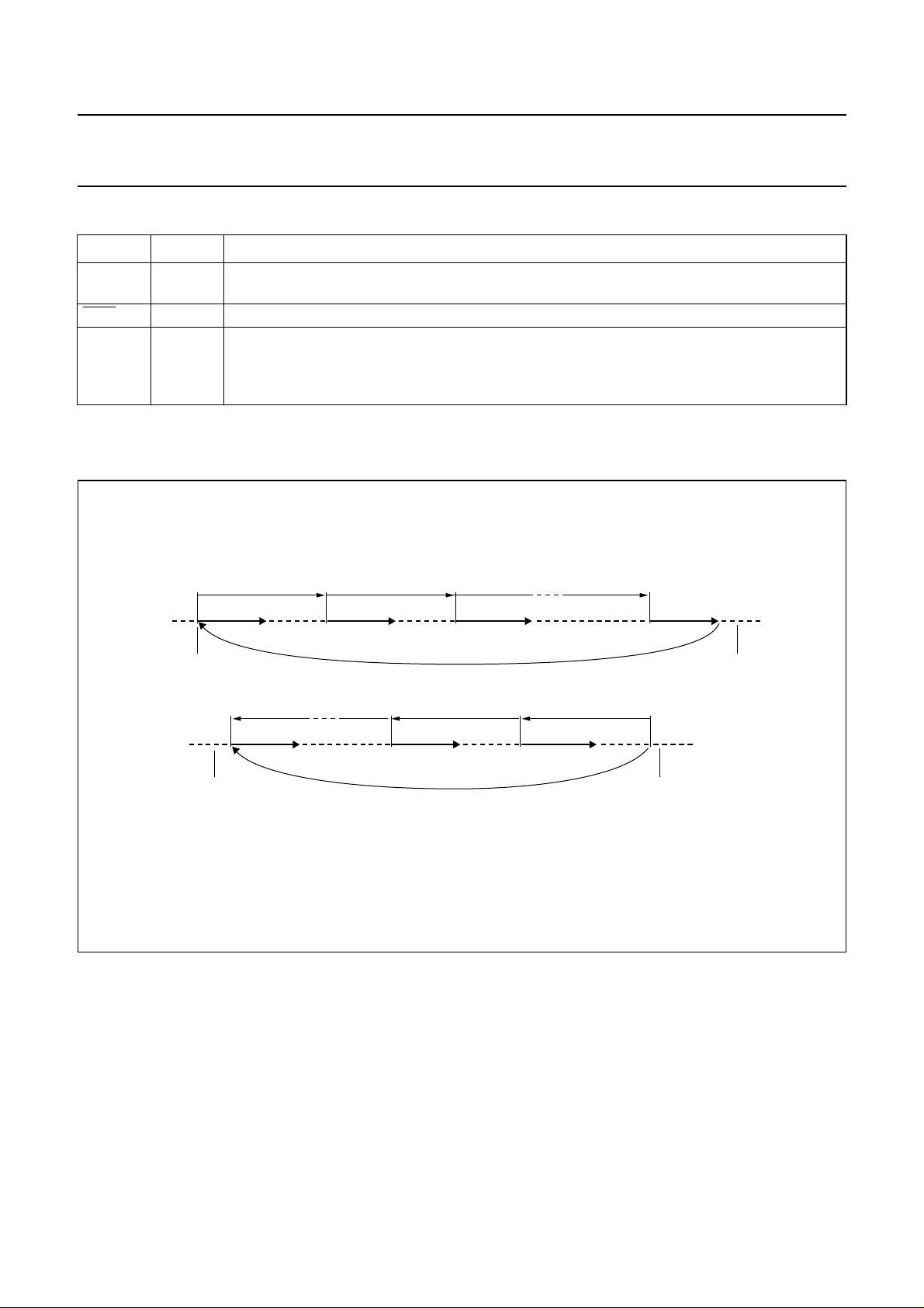
If the Protection Violation (PV) handling bit and the limit
register are reset, the following data will be ignored until
detection of the End-Of-Window (EOW) signal. In read
mode the DMA control also waits for this signal, to start the
next data transfer. If the PV bit is set, the input of the FIFO
will be locked and the FIFO will be emptied. If the FIFO is
empty the TR_E bit is reset. This feature could be used for
a single capture mode, if the protection address is the
same address as the last pixel in this field. With that, the
SAA7146A will write one field into system memory and
then stop.
If the limit register of any DMA channel (video, VBI data or
audio) has a value other than ‘0000’ the continuous write
mode is chosen. If the actual PCI address hits the
protection address and the PV bit is zero, the FINC stops
the current transfer, sets an interrupt and resets the actual
address to the base address. Regarding this, the
protection address could be used to define a memory
space to which data is sent. The SAA7146A offers the
possibility to monitor the filling level of this memory space.
The limit register defines an address limit, which generates
an interrupt if passed by the actual PCI address pointer.
‘0001’ means an interrupt will be generated if the lower
6 bits (64 bytes) of the PCI address are zero. ‘0010’
defines a limit of 128 bytes, ‘0011’ one of 256 bytes, and
so on up to 1 Mbyte defined by ‘1111’. This interrupt range
can be calculated as follows:
Range = 2
The protection handling modes such as those selected by
the PV bit and the contents of the limit register are shown
in Table 4.
(5 +Limit)
bytes.
1998 Apr 09 24
Page 25
Philips Semiconductors Product specification
Multimedia bridge, high performance
SAA7146A
Scaler and PCI circuit (SPCI)
Table 4 Protection violation handling modes
LIMIT PV DESCRIPTION
0000 0 Lock input of FIFO and empty FIFO (only in write mode). Unlock FIFO and start next transfer
using the base address at the detection of BOF.
0000 0 Restart immediately at base address.
(1)
XXXX
Note
1. X = don’t care.
handbook, full pagewidth
1 Lock input of FIFO, empty FIFO (only in write mode) and then reset TR_E bit. The next transfer
starts with BOF using the corresponding base address, if the TR_E bit is set again. This setting
is useful for single-shot, that means transferring only one frame of a video stream. Therefore
the protection address has to be the same as the address of the last pixel of the field.
positive pitch
positive pitch
positive pitch
Last line
BaseAddr
BaseAddr
ProtAddr
1st line
negative pitch
Last line
2nd line
3rd line
(a) positive line pitch
negative pitch
2nd line
(b) positive line pitch
negative pitch
1st line
Fig.5 Handling of base and protection address using positive and negative line pitch.
ProtAddr
MGG260
1998 Apr 09 25
Page 26

Philips Semiconductors Product specification
Multimedia bridge, high performance
SAA7146A
Scaler and PCI circuit (SPCI)
7.2.3 AUDIO DMA CONTROL
The SAA7146A provides up to four audio DMA channels,
each using a FIFO of 24 Dwords. Two channels are read
only (A1_in and A2_in) and two channels are write only
(A1_out and A2_out). Because audio represents a
continuous data stream, which is neither line nor field
dependent, the audio DMA control offers only one base
address (BaseAxx) and no pitch register. For FIFO
overflow and underflow the handling of these channels is
done in the same way as the video DMA channels
(see Section 7.2.2).
Table 5 Audio DMA control register
OFFSET
(HEX)
94 BaseA1_in 31 to 0 RW base address for audio input Channel 1; this value specifies a
98 ProtA1_in 31 to 2 RW protection address for audio input Channel 1; this address
9C PageA1_in 31 to 12 RW base address of the page table, see Section 7.2.4.
A0 BaseA1_out 31 to 0 RW Base address for audio output Channel 1; this value specifies a
A4 ProtA1_out 31 to 2 RW protection address for audio output Channel 1; this address
A8 PageA1_out 31 to 12 RW base address of the page table, see Section 7.2.4.
NAME BIT TYPE DESCRIPTION
byte address
could be used to specify a upper limit for audio access in memory
space
− 1to0 − reserved
MEA1_in 11 RW mapping enable; this bit enables the MMU
− 10 to 8 − reserved
LimitA1_in 7 to 4 RW interrupt limit; defines the size of the memory range, that
generates interrupt, if its boundaries are passed
PVA1_in 3 RW protection violation handling
− 2to0 − reserved
byte address. The lower two bits are forced to zero.
could be used to specify a upper limit for audio access in memory
space
− 1 and 0 − reserved
MEA1_out 11 RW mapping enable; this bit enables the MMU
− 10 to 8 − reserved
LimitA1_out 7 to 4 RW interrupt limit; defines the size of the memory range, that
generates an interrupt, if its boundaries are passed
PVA1_out 3 RW protection violation handling
− 2to0 − reserved
The protection violation handling differs only if the limit
register and the PV bit are programmed to zero. The audio
DMA channel does not wait for the EOF signal, like the
video ones. It does not generate interrupts. The interrupt
range specified by the limit register is defined in the same
way as described in Section 7.2.2. The audio DMA
channels try immediately to transfer data after setting the
transfer enable bits. All registers for audio DMA control,
which are the base address, the protection address and
the control bits are listed in the following Table 5, except
the input control bits (Burst, Threshold), which are listed in
Table 6.
1998 Apr 09 26
Page 27

Philips Semiconductors Product specification
Multimedia bridge, high performance
SAA7146A
Scaler and PCI circuit (SPCI)
OFFSET
(HEX)
AC BaseA2_in 31 to 0 RW Base address for audio input Channel 2; this value specifies a
B0 ProtA2_in 31 to 2 RW protection address for audio input Channel 2; this address
B4 PageA2_in 31 to 12 RW base address of the page table, see Section 7.2.4
B8 BaseA2_out 31 to 0 RW Base address for audio output Channel 2; this value specifies a
BC ProtA2_out 31 to 2 RW protection address for audio output Channel 2; this address
C0 PageA2_out 31 to 12 RW base address of the page table, see Section 7.2.4
NAME BIT TYPE DESCRIPTION
byte address. The lower two bits are forced to zero.
could be used to specify a upper limit for audio access in memory
space
− 1 and 0 − reserve
MEA2_in 11 RW mapping enable; this bit enables the MMU
− 10 to 8 − reserved
LimitA2_in 7 to 4 RW interrupt limit; defines the size of the memory range, that raise an
interrupt, if its boundaries are passed
PVA2_in 3 RW protection violation handling
− 2to0 − reserve
byte address. The lower two bits are forced to zero.
could be used to specify a upper limit for audio access in memory
space
− 1 and 0 − reserved
MEA2_out 11 RW mapping enable; this bit enables the MMU
− 10 to 8 − reserved
LimitA2_out 7 to 4 RW interrupt limit; defines the size of the memory range, that raise an
interrupt, if its boundaries are passed
PVA2_out 3 RW protection violation handling
− 2to0 − reserved
1998 Apr 09 27
Page 28

Philips Semiconductors Product specification
Multimedia bridge, high performance
Scaler and PCI circuit (SPCI)
7.2.4 MEMORY MANAGEMENT UNIT (MMU)
7.2.4.1 Introduction
To perform DMA transfers, physically continuous memory
space is needed. However, operating systems such as
Microsoft Windows are working with virtual demand
paging, using a MMU to translate linear to physical
addresses. Memory allocation is performed in the linear
address space, resulting in fragmented memory in the
physical address space. There is no way to allocate large
buffers of physical, continuous memory, except reserving
it during system start-up. Thus decreasing the system
performance dramatically. To overcome this problem the
SAA7146A contains a Memory Management Unit (MMU)
as well. This MMU is able to handle memory fragmented
to 4 kbyte pages, similar to the scheme used by the Intel
8086 processor family. The MMU can be bypassed to
simplify transfers to non-paged memory such as the
graphics adapter’s frame buffer.
7.2.4.2 Memory allocation
The SAA7146A’s MMU requires a special scheme for
memory allocation. The following steps have to be
performed:
• Allocation of n pages, each page being 4 kbytes of size,
aligned to a 4 kbyte boundary
• Allocation of one extra page, to be used as page table
• Initialization of the page table.
Allocation of pages is done in physical address space.
Operating systems implementing virtual memory provide
services to allocate and free these pages.
SAA7146A
The page table is stored in a separate page. This limits the
linear address page to a size of 4 Mbytes and results in a
4 kbyte overhead. The page table is organized as an array
of n Dwords, with each entry giving the physical address of
one of the n pages of allocated memory. As pages are
aligned to 4 kbytes, the lower 12 bits of each entry are
fixed to zero.
7.2.4.3 Implementation
The SAA7146A has up to 8 DMA channels (3 video,
4 audio and 1 DEBI channel) for which the memory
mapping is done. Each of them provides the linear address
to (from) which it wants to send (read) data during the next
transfer. Their register sets contain a page table base
address (Pagexx) and a mapping enable bit (MExx).
If MExx is set, mapping is enabled.
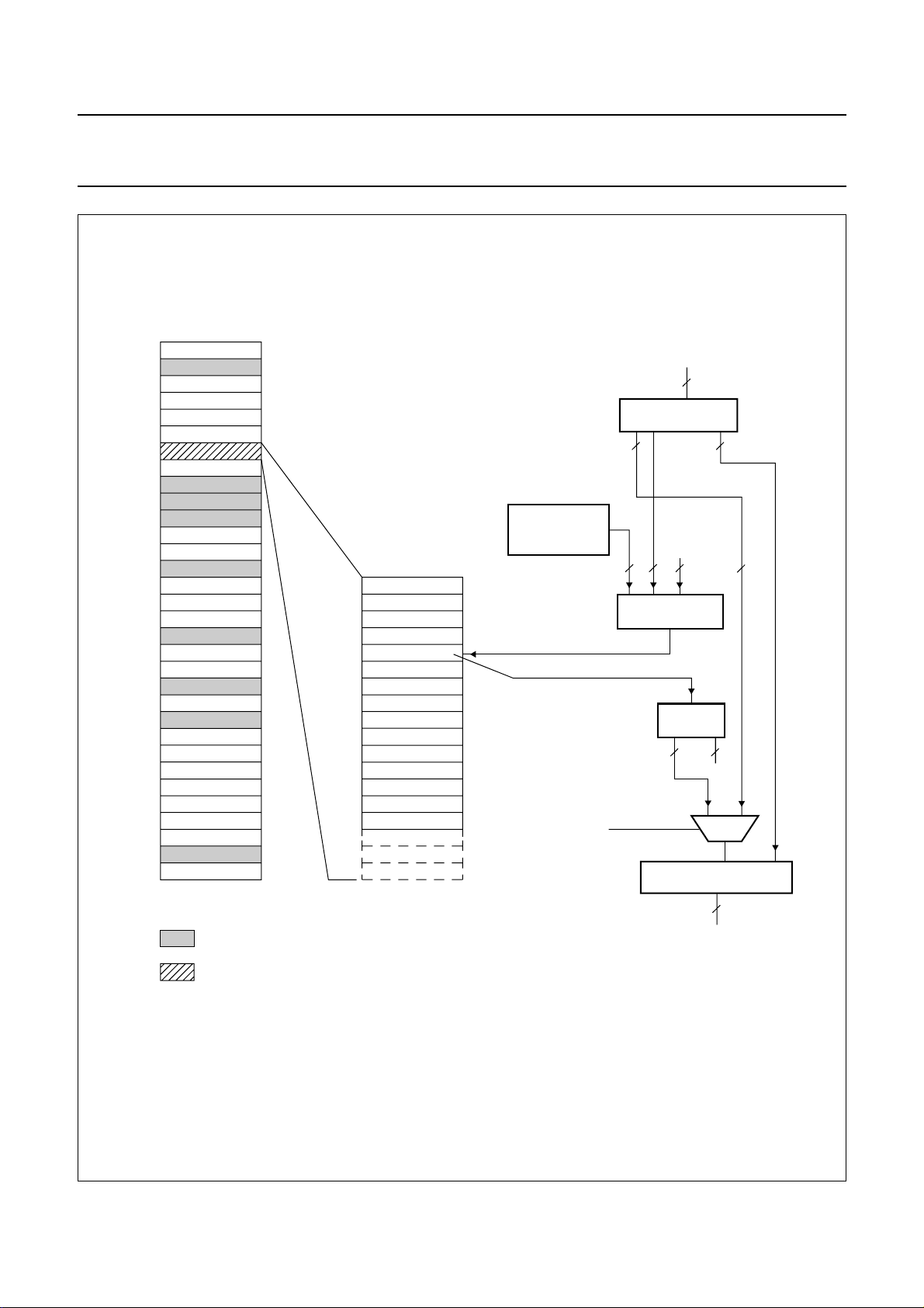
The MMU checks for each channel whether its address
has been already translated. If translated, its request can
pass to the Internal Arbitration Control (INTAC) managing
the access to the PCI-bus. If not, the MMU starts a bus
transfer to the page table. The page table entry address
could be calculated from the channels PCI address and
the page table base address, as shown in Fig.6. The upper
20 bits of the PCI address are replaced by the upper
20 bits of the according page address to generate the
mapped PCI address.
If the PCI address crosses a 4 kbyte boundary during a
transfer, the MMU stops this transfer and suppresses its
request to the INTAC until it has renewed the page
address, which means replacing the upper 20 bits of the
current address. To reduce latency the SAA7146A will do
a pre-fetch, i.e. it will always try to load the next page
address in advance.
1998 Apr 09 28
Page 29
Philips Semiconductors Product specification
Multimedia bridge, high performance
Scaler and PCI circuit (SPCI)
handbook, full pagewidth
00000H
00007H
0000FH
00017 H
Physical memory
(4 kbyte pages)
000H
007H
Page table
00001000H
00008000H
00009000H
0000A000H
0000D000H
00011000H
00014000H
00016000H
0001E000H
PAGE TABLE
BASE ADDRESS
(00006H)
32
DMA ADDRESS
'0'
202010
PAGE TABLE
ENTRY ADDRESS
2
PAGE
ADDRESS
SAA7146A
1210
1220
015H
0001FH
= allocated memory space
= page table
Fig.6 Memory Management Unit (MMU).
1998 Apr 09 29
ME
(Mapping Enable)
PHYSICAL PCI ADDRESS
32
MGG261
Page 30

Philips Semiconductors Product specification
Multimedia bridge, high performance
Scaler and PCI circuit (SPCI)
7.2.5 INTERNAL ARBITRATION CONTROL
The SAA7146A has up to three video DMA channels, four
audio DMA channels and three other DMA channels (RPS,
MMU and DEBI) each trying to get access to the PCI-bus.
To handle this, an Internal Arbitration Control (INTAC) is
needed. INTAC controls on the one hand the PCI-bus
requests and on the other hand the order in which each
DMA channel gets access to the bus.
The basic implementation of the internal arbitration control
is a round-robin mechanism on the top, consisting of the
RPS, the MMU and one of the eight data channels. Data
channel arbitration is performed using a ‘first come first
serve’ queue architecture, which may consist of up to eight
entries.
Each data channel reaching a certain filling level of its
FIFO defined by the threshold, is allowed to make an entry
into the arbitration queue. The threshold defines the
number of Dwords needed to start a sensible PCI transfer
and must be small enough to avoid a loss of data due to an
overflow regarding the PCI latency time. After each job
(Video Transfer Done, VTD) the video channels have to be
emptied and are allowed to fill an entry into the queue,
even if they have not yet reached their threshold.
Concurrently to the entry the channel sets a bit which
prohibits further entries to this channel. In the worst case,
each data channel can have only one entry in the queue.
If each channel wants to access the bus, which means the
queue is full, an order like the one shown below will be
given.
• MMU
• RPS.
SAA7146A
First entry of the data channel queue:
• MMU
• RPS.
Second entry of the data channel queue:
• MMU
• and so on.
If INTAC detects at least one DMA channel in the queue or
an MMU or an RPS request, it signals the need for the bus
by setting the REQ# signal on the PCI-bus. If the GNT#
signal goes LOW, the SAA7146A is the owner of the bus
and makes the PCI master module working with the first
channel selected. The master module tries to transfer the
number of Dwords defined in the Burst Register. For RPS
the burst length is hardwired to four and for the MMU it is
hardwired to two Dwords. After that the master module
stops this transfer and starts a transfer using the next
channel (due to the round-robin).
If a DMA channel gets its transfer stopped due to a retry,
the arbitration control sets the corresponding retry flag.
INTAC tries to end a retried transfer, even if this transfer
gets stopped via the Transfer Enable bit (TR_E). For this
reason the Transfer Enable bits are internally shadowed
by INTAC. A transfer can only be stopped if it has no retry
pending.
The Arbitration Control Registers (Burst and Threshold of
DEBI, Video 1 to 3, Audio 1 to 4) are listed in Table 6.
1998 Apr 09 30
Page 31
Philips Semiconductors Product specification
Multimedia bridge, high performance
Scaler and PCI circuit (SPCI)
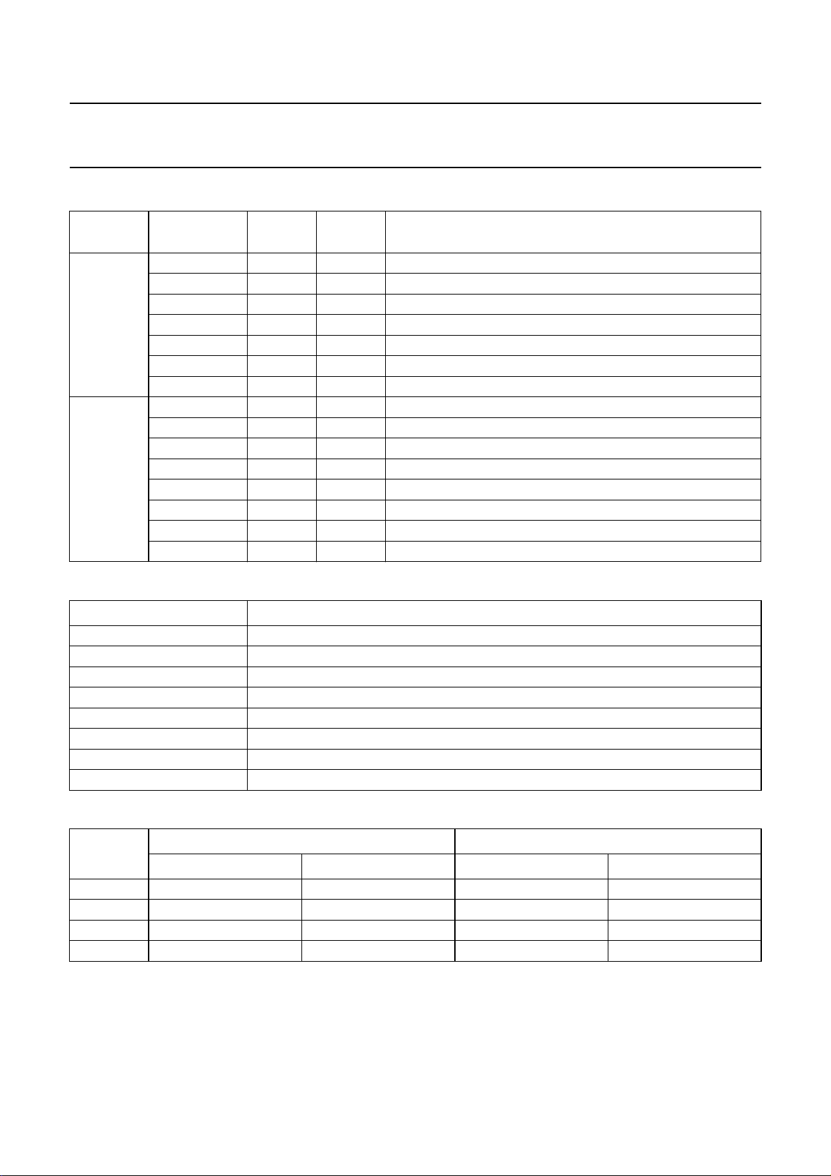
Table 6 Arbitration control registers
OFFSET
(HEX)
48 BurstDebi 28 to 26 RW PCI burst length of the DEBI DMA channel; see Table 7
4C BurstA1_in 28 to 26 RW PCI burst length of audio input Channel 1; see Table7
NAME BIT TYPE DESCRIPTION
Burst3 20 to 18 RW PCI burst length of video Channel 3; see Table 7
Thresh3 17 to 16 RW threshold of FIFO3; see Table 8
Burst2 12 to 10 RW PCI burst length of video Channel 2; see Table 7
Thresh2 9 to 8 RW threshold of FIFO 2; see Table 8
Burst1 4 to 2 RW PCI burst length of video Channel 1; see Table 7
Thresh1 1 and 0 RW threshold of FIFO 1; see Table 8
ThreshA1_in 25 to 24 RW threshold of audio FIFO A1_in; see Table 8
BurstA1_out 20 to 18 RW PCI burst length of audio output Channel 1; see Table 7
ThreshA1_out 17 and 16 RW threshold of audio FIFO A1_out; see Table 8
BurstA2_in 12 to 10 RW PCI burst length of audio input Channel 2; see Table 7
ThreshA2_in 9 and 8 RW threshold of audio FIFO A2_in; see Table 8
BurstA2_out 4 to 2 RW PCI burst length of audio output Channel 2; see Table 7
ThreshA2_out 1 and 0 RW threshold of audio FIFO A2_out; see Table 8
SAA7146A
Table 7 Burst length definition
VALUE BURST LENGTH
000 1 Dword
001 2 Dwords
010 4 Dwords
011 8 Dwords
100 16 Dwords
101 32 Dwords
110 64 Dwords
111 128 Dwords
Table 8 Threshold definition
VALUE
WRITE MODE
VIDEO AUDIO VIDEO AUDIO
00 4 Dwords of valid data 1 Dword of valid data 4 empty Dwords 1 empty Dword
01 8 Dwords of valid data 4 Dwords of valid data 8 empty Dwords 4 empty Dwords
10 16 Dwords of valid data 8 Dwords of valid data 16 empty Dwords 8 empty Dwords
11 32 Dwords of valid data 16 Dwords of valid data 32 empty Dwords 16 empty Dwords
Note
1. The threshold is reached, if the FIFO contains at least this number of Dwords.
(1)
READ MODE
(1)
1998 Apr 09 31
Page 32
Philips Semiconductors Product specification
Multimedia bridge, high performance
SAA7146A
Scaler and PCI circuit (SPCI)
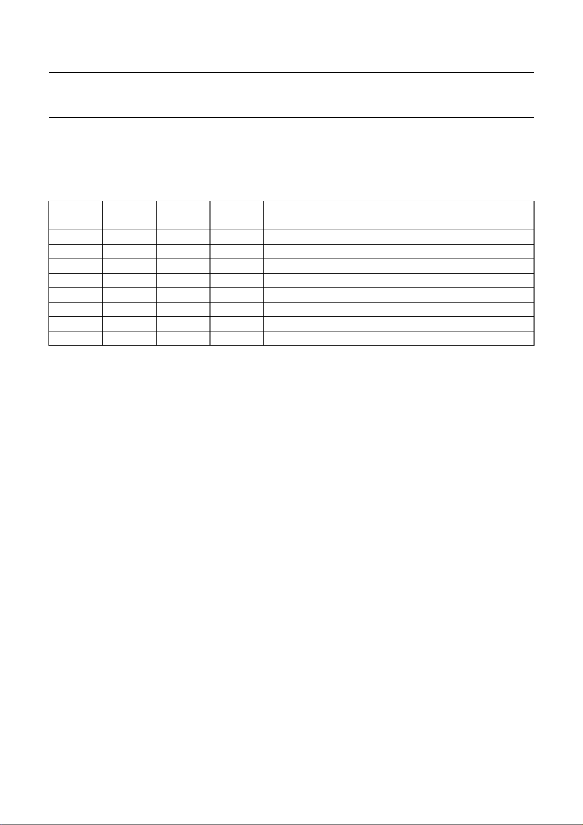
7.2.6 STATUS INFORMATION OF THE PCI INTERFACE
Table 9 lists the status information that the PCI interface makes available to the user in addition to the interrupt sources
that are described later. This information is read only.
Table 9 Status bits of the DMA control
OFFSET
(HEX)
120 VDP1 31 to 0 R logical video DMA pointer of FIFO 1
124 VDP2 31 to 0 R logical video DMA pointer of FIFO 2l
128 VDP3 31 to 0 R logical video DMA pointer of FIFO 3
12C ADP1 31 to 0 R logical audio DMA pointer of audio output FIFO A1_out
130 ADP2 31 to 0 R logical audio DMA pointer of audio input FIFO A1_in
134 ADP3 31 to 0 R logical audio DMA pointer of audio output FIFO A2_out
138 ADP4 31 to 0 R logical audio DMA pointer of audio input FIFO A2_in
13C DDP 31 to 0 R logical DEBI DMA pointer
7.3 Main control
7.3.1 G
The SAA7146A has two Dwords of general control to
support quick enable/disable switching of any activity of
the SAA7146A via direct access by the CPU. These main
control Dwords are split in two parts. The upper parts have
16 bits of bit-mask to allow bit-selective write to the lower
part which contains single bit enable/disable control of
major interface functions of SAA7146A. If a certain bit
position is masked with a logic 1 in the mask word (upper
2 bytes) during a write access, then the corresponding bit
in the control word (lower 2 bytes) is changed according to
the contents of the transmitted data. By that the CPU can
easily switch on or off certain selected interfaces of the
SAA7146A without checking the actual ‘remaining’
programming (enabling) of the other parts.
NAME BIT TYPE DESCRIPTION
The programming of registers for the 3 Video DMA
ENERAL
channels, both video processors (HPS, BRS) and for the
interfaces DEBI and I
method. This is done to guarantee coherent programming
data. During initiation of an upload operation from a
shadow RAM each of the UPLD bits [10 to 0] (see
Table 11) is assigned to a set of registers. If a logic 1 is
written into a UPLD bit all dedicated shadow RAM
registers containing changed data are uploaded into their
working registers immediately. During a read cycle the
UPLD bits give information on whether the shadow RAM
contains changed data not yet uploaded into the working
registers. The UPLD bits remain HIGH as long as the
contents of the shadow RAM represents the current
programming
2
C-bus is performed by an upload
1998 Apr 09 32
Page 33
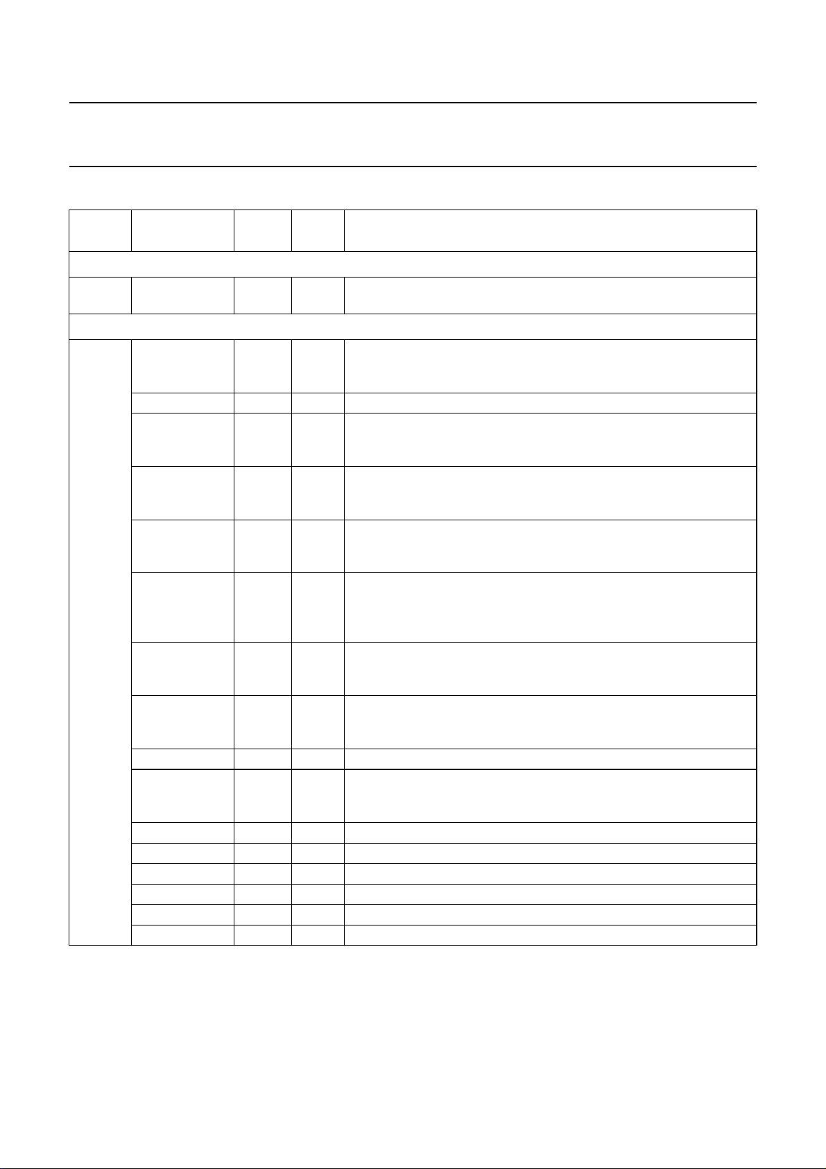
Philips Semiconductors Product specification
Multimedia bridge, high performance
SAA7146A
Scaler and PCI circuit (SPCI)
Table 10 Main control register 1
OFFSET
(HEX)
Mask word
FC M15 to M00 31 to 16 RW 16-bit mask word for bit-selective writes to the control word; when
Control word
FC MRST_N 15 RW Master Reset Not: this is the master reset for the SAA7146A. Writing
NAME BIT TYPE DESCRIPTION
read these bits always return logic 0
a logic 0 to this bit will reset the SAA7146A to the same state as after
a power-on reset. When read this bit always returns a logic 0.
− 14 − reserved: when read this bit always returns a logic 0
ERPS1 13 RW Enable Register Program Sequencer Task 1: if ERPS1 = 1, then
any RPS Task 1 action is enabled. If ERPS1 = 0, then RPS Task 1
action does not fetch any more commands.
ERPS0 12 RW Enable Register Program Sequencer Task 0: if ERPS0 = 1, then
any RPS Task 0 action is enabled. If ERPS0 = 0, then RPS Task 0
action does not fetch any more commands.
EDP 11 RW Enable DEBI Port pins: if EDP = 0, all pins of the DEBI port are set
to 3-state. If EDP = 1, then the function of all pins at the DEBI port is
as programmed via the DEBI registers.
EVP 10 RW Enable Real Time Video Ports pins: if EVP = 0, all 24 pins of the
real time video interface (DD1 port) are 3-stated. If EVP = 1, then the
function of all pins at the real time video interface (DD1 port) is as
programmed by the scaler register; see Table 66.
EAP 9 RW Enable Audio Port pins: if EAP = 0, all 14 pins of the audio interface
port are set to 3-state. If EAP = 1, then the function of all pins at the
audio interface is as programmed in Section 7.16.3.
EI2C 8 RW Enable I
interface port are set to 3-state. If EI2C = 1, then the I2C-bus interface
is enabled and will function as programmed in Section 7.17.2.
TR_E_DEBI 7 RW Transfer Enable bit of the DEBI.
TR_E_1 6 RW Transfer enable bit of video Channel 1: if set this channel is included
in the internal arbitration scheme. If not set, this channel will be
ignored and no transfer will start using this FIFO.
TR_E_2 5 RW Transfer Enable bit of video channel 2
TR_E_3 4 RW Transfer Enable bit of video channel 3
TR_E_A2_OUT 3 RW Transfer Enable bit of audio channel 2 out
TR_E_A2_IN 2 RW Transfer Enable bit of audio channel 2 in
TR_E_A1_OUT 1 RW Transfer Enable bit of audio channel 1 out
TR_E_A1_IN 0 RW Transfer Enable bit of audio channel 1 in
2
C Port pins: if EI2C = 0, then both pins of the I2C-bus
1998 Apr 09 33
Page 34
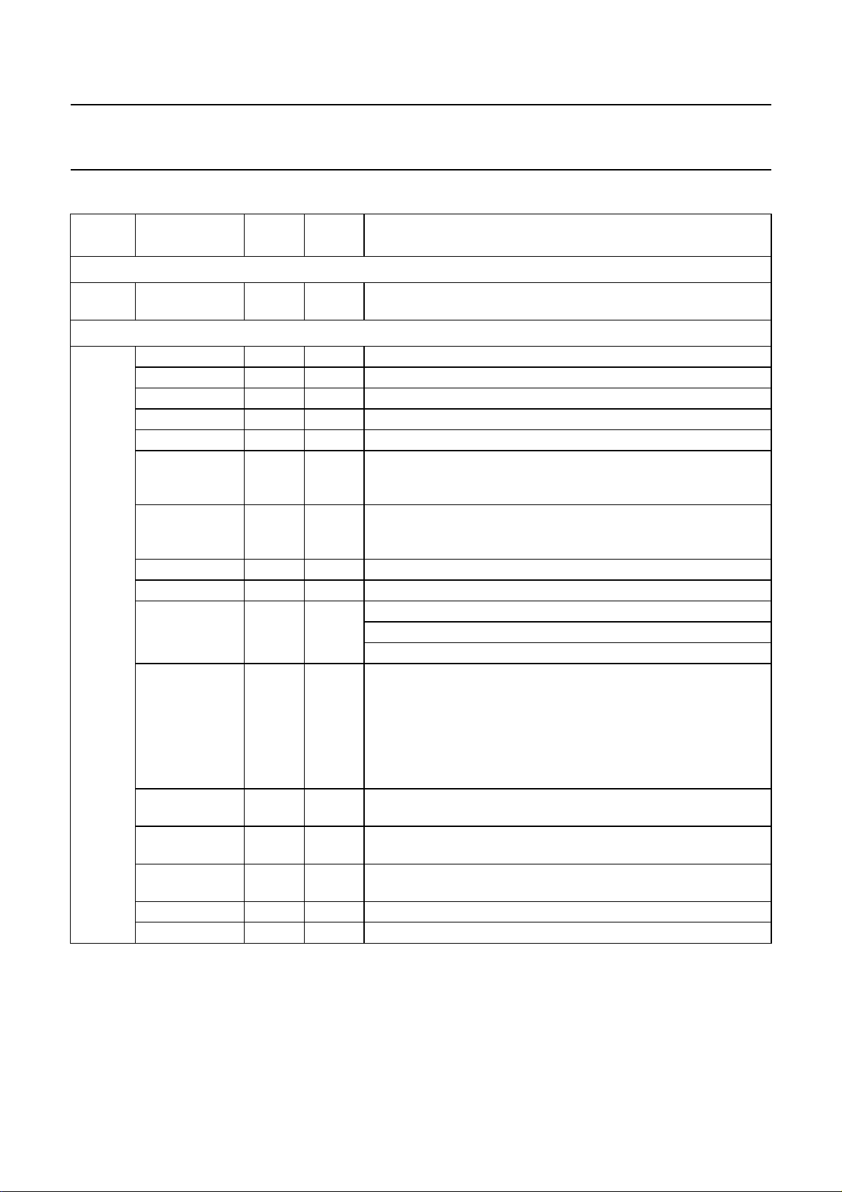
Philips Semiconductors Product specification
Multimedia bridge, high performance
SAA7146A
Scaler and PCI circuit (SPCI)
Table 11 Main control register 2
OFFSET
(HEX)
Mask word
100 M15 to M00 31 to 16 RW 16-bit mask word for bit-selective writes to the control word; when
Control word
100 RPS_SIG4 15 RW RPS Signal 4
NAME BIT TYPE DESCRIPTION
read this bits always returns logic 0
RPS_SIG3 14 RW RPS Signal 3
RPS_SIG2 13 RW RPS Signal 2
RPS_SIG1 12 RW RPS Signal 1
RPS_SIG0 11 RW RPS Signal 0
UPLD_D1_B 10 RW Upload ‘Video DATA stream handling at port D1_B (54H)’; see
Table 68. To upload ‘Initial setting of Dual D1 Interface (50H)’, this
bit and bit 9 must be set; see Table 66.
UPLD_D1_A 9 RW Upload ‘Video DATA stream handling at port D1_A (54H)’; see
Table 67. To upload ‘Initial setting of Dual D1 Interface (50H)’, this
bit and bit 10 must be set; see Table 66.
UPLD_BRS 8 RW Upload ‘BRS Control Register (58H)’; see Table 69.
− 7 − Reserved; when read this bit always returns a logic 0.
UPLD_HPS_H 6 RW Upload ‘HPS Horizontal prescale (68H)’; see Table 79.
Upload ‘HPS Horizontal fine-scale (6CH)’; see Table 81.
Upload ‘BCS control (70H)’; see Table 82.
UPLD_HPS_V 5 RW Upload ‘HPS control (5CH)’; see Table 71.
Upload ‘HPS Vertical scale (60H)’; see Table 72.
Upload ‘HPS Vertical scale and gain (64H)’; see Table 73.
Upload ‘Chroma Key range (74H)’; see Table 86.
Upload ‘HPS Outputs and Formats (78H)’; see Table 87.
Upload ‘Clip control (78H)’; see Table 89.
UPLD_DMA3 4 RW Upload ‘Video DMA3 registers’; 30H, 34H, 38H, 3CH, 40H, 44H
and 48H (20 to 16).
UPLD_DMA2 3 RW Upload ‘Video DMA2 registers’; 18H, 1CH, 20H, 24H, 28H, 2CH
and 48H (12 to 8).
UPLD_DMA1 2 RW Upload ‘Video DMA1 registers’; 00H, 04H, 08H, 0CH, 10H, 14H
and 48H (4 to 0).
UPLD_DEBI 1 RW Upload ‘DEBI registers’; 88H, 7CH, 80H, 84H and 48H (28 to 26).
UPLD_IIC 0 RW Upload ‘I
2
C-bus registers’; (8CH and 90H).
1998 Apr 09 34
Page 35

Philips Semiconductors Product specification
Multimedia bridge, high performance
Scaler and PCI circuit (SPCI)
7.4 Register Programming Sequencer (RPS)
The RPS is used as an additional method to program or
read the registers of the SAA7146A. Its main function is
programming the registers on demand without delay via
the interrupt handler of the host system.
Because different applications of the SAA7146A can run
independently on and asynchronously to each other the
RPS is capable of running two parallel tasks. Both tasks
are completely equal to each other and each has its own
set of registers (RPS address, RPS page, HBI threshold
and RPS time out value). Each task can be separately
enabled by setting its related ERPSx bit in the Main control
register 1 (see Table 10). To allow communication
between both tasks and the CPU there are five signals
which can be set or reset from both tasks (see Table 11).
The programming of a task is defined by an instruction list
in the system main memory that consists of RPS
commands. The operation of the RPS is initiated on
command by setting the ERPS bit of the desired task in the
Main control register 1.
SAA7146A
The processing of RPS can be controlled by a sequence
of wait commands on special events. Furthermore the
program flow can be controlled via conditional jumps
related to the communication with the host setting
semaphores or special internal interrupts.
7.4.1 RESET
During a reset the ERPSx (Enable RPS of task ‘x’) bits in
the Main control register 1 (see Table 10) of the
SAA7146A are cleared so that an RPS task has to be
explicitly started.
7.4.2 E
Table 12 shows the events available during the execution
of an RPS program. The execution can for example wait
on these events to become true. In general these events
are set if a rising edge of the corresponding signal occurs
and are cleared if a falling edge of the signal occurs.
If signals are logic HIGH after the reset and no rising edge
occurs the corresponding event (available in an RPS
program execution) will not be set.
VENT DESCRIPTION
Table 12 Description of events
EVENT DESCRIPTION
IICD IIC Done: Done flag of the I
DEBID DEBI Done: Done flag of DEBI; see note 1
O_FID_A; O_FID_B Field Identification signal: for an odd field dependent on sync detection at Port A/Port B
E_FID_A; E_FID_B Field Identification signal: for an even field dependent on sync-detection at Port A/Port B
HS HPS Source: wait for processing of source line before line addressed by SLCT is done
HT HPS Target: wait for processing of target line before line addressed by TLCT is done
VBI_A; VBI_B Vertical Blanking Indicator at Port A/Port B: for details on this signal see Table 90
BRS_DONE Inactive BRS data path: for details on this signal see Table 90
HPS_DONE Inactive HPS data path between two windows: for details on this signal see Table 90
HPS_LINE_DONE Inactive HPS data path between two lines: for details on this signal see Table 90
VTD1; VTD2; VTD3 Video T ransfer Done: video DMA 1, video DMA 2 or video DMA 3 has transferred a complete
window and is ready to be reprogrammed
GPIO0 General Purpose I/O 0: this bit reflects the status of the GPIO pin 0
GPIO1 General Purpose I/O 1: this bit reflects the status of the GPIO pin 1
GPIO2 General Purpose I/O 2: this bit reflects the status of the GPIO pin 2
GPIO3 General Purpose I/O 3: this bit reflects the status of the GPIO pin 3
SIGx General purpose signal x: for intertask and RPS to CPU communication or program flow
control. ‘x’ can take a value within the range 0 to 4
Note
1. If an RPS program is used to make DEBI transfer consecutive data blocks employ the following commands: LOAD
REGISTER, CLEAR SIGNAL, UPLOAD and PAUSE. Before uploading the register contents the DEBI_DONE flag
of a former transfer has to be cleared. With this, the following PAUSE command waits correctly for DEBI_DONE of
the just started DEBI block transfer.
2
C-bus
1998 Apr 09 35
Page 36

Philips Semiconductors Product specification
Multimedia bridge, high performance
Scaler and PCI circuit (SPCI)
7.4.3 COMMAND LIST
An instruction list of an RPS task is built in the system
memory by the device driver. This list is made up of
command sequences; each command being at least one
Dword long. The first Dword of a command consists of the
instruction code (4-bit) and a command specific part
(28 bits). Commands longer than one Dword contain data
in the additional Dwords.
Table 13 Command Dword
D31 to D28 D27 to D0
Instruction code command specific
7.4.4 T
The instruction code identifies one of the following
commands (see bits 31 to 28 of Tables 14 to 29).
7.4.4.1 PAUSE
The PAUSE command is a one Dword command. This
command contains in the command specific part the
events to wait for; see Tables 14 and 15. The execution of
the RPS task is delayed until the condition addressed via
the events becomes true or a time out occurs.
To control the time a PAUSE command stays in the wait
state, it is possible to set a RPS time out value. This value
specifies after how many PCI clocks and/or V_syncs a
time out will be asserted. When it occurs the RPS_TO bits
in the PSR (see Table 38) is set and if enabled an interrupt
will be generated. However, the RPS will stop this task.
The OAN bit specifies if the condition in bits 25 to 0 is an
AND (OAN set to 0) or if the condition is an OR (OAN set
to 1). If the INV bit is set this command will wait for the
condition to become false.
7.4.4.2 UPLOAD
The UPLOAD command is a one Dword-command. This
command contains in the command specific part the
sections to be uploaded from the shadow RAM to the
working registers, see Tables 16 and 17.
HE INSTRUCTION CODE
SAA7146A
7.4.4.3 CHECK-LATE
The CHECK_LATE command is a one Dword-command.
This command contains in the command specific part the
events to check and if necessary to wait for, as shown in
Tables 18 and 19. The execution of the RPS task is
delayed until the condition addressed via the events
becomes true, or a time out occurs and the upload is
performed.
The OAN bit specifies if the condition in bits 25 to 0 is an
AND (OAN set to 0) or if the condition is an OR (OAN set
to 1). If the INV bit is set this command will wait for the
condition to become false.
If the CHECK_LATE command finds that the wait
condition is already true the RPS-LATE is set. Otherwise it
waits for the condition as the PAUSE command. A time out
behaviour such as described for the PAUSE command is
also supplied.
7.4.4.4 CLR_SIGNAL
The CLR_SIGNAL Command clears the selected signals.
This will not affect the real status bits of the SAA7146A.
Only a copy of this bit related to the RPS will be cleared.
It will be set again via a SET_SIGNAL command or when
the real status will be set due to normal processing.
The CLR_SIGNAL format is shown in Tables 20 and 21.
7.4.4.5 NOP
The NOP command consists of one Dword and has the
instruction code 0000. All bits of the command specific
part have to be set to zero. This command is a special
case of the CLR_SIGNAL command!
7.4.4.6 SET_SIGNAL
The SET_SIGNAL command sets the selected signals.
If one of the SAA7146A status related signals is selected
to be set, it will not affect the real status bit of the
SAA7146A. Only a copy of this bit related to the RPS, will
be set. The SET_SIGNAL format is shown in
Tables 22 and 23.
If the UPLOAD command finds a bit of a section set it
uploads the corresponding registers from the shadow
RAM to the working registers. This is done for registers
with changed shadow RAM values only.
1998 Apr 09 36
Page 37

Philips Semiconductors Product specification
Multimedia bridge, high performance
Scaler and PCI circuit (SPCI)
7.4.4.7 INTERRUPT
The INTERRUPT command will set the RPS_I bit of the
task in the Interrupt status register (see Table 41) if it is
executed and the condition described by the event flags is
true. The execution of RPS continues. The format of the
Interrupt command is shown in Tables 24 and 25.
The OAN bit specifies if the condition in bits 25 to 0 is an
AND (OAN set to 0) or if the condition is an OR (OAN set
to 1). If the INV bit is set this command will wait for the
condition to become false.
7.4.4.8 STOP
The STOP command will terminate the RPS execution and
reset the ERPS-bit. The command specific part of the
STOP command is like the INTERRUPT command. If the
addressed event is true the STOP will be executed
otherwise the execution will continue with the next
command. If no event is addressed the STOP will be
executed unconditionally. The format of the STOP
command is shown in Tables 26 and 27.
SAA7146A
7.4.4.9 JUMP
The JUMP command is a two Dword command.
The second Dword contains the physical address at which
the RPS will continue its execution. The address in the
second Dword is directly transferred to the RPSAddr
Register. The command specific part in the first Dword of
the JUMP command is like the INTERRUPT command.
If the addressed event is true the JUMP will be performed
otherwise the execution will continue at the next
command. If no event is addressed the JUMP will be
unconditional. The format of the JUMP command is shown
in Tables 28 and 29.
The OAN bit specifies if the condition in bits 25 to 0 is an
AND (OAN set to 0) or if the condition is an OR (OAN set
to 1). If the INV bit is set this command will wait for the
condition to become false.
The OAN bit specifies if the condition in bits 25 to 0 is an
AND (OAN set to 0) or if the condition is an OR (OAN set
to 1). If the INV bit is set this command will wait for the
condition to become false.
1998 Apr 09 37
Page 38
This text is here in white to force landscape pages to be rotated correctly when browsing through the pdf in the Acrobat reader.This text is here in
_white to force landscape pages to be rotated correctly when browsing through the pdf in the Acrobat reader.This text is here inThis text is here in
white to force landscape pages to be rotated correctly when browsing through the pdf in the Acrobat reader. white to force landscape pages to be ...
1998 Apr 09 38
Table 14 PAUSE command format
D31 TO D28 D27 D26 D25 D24 D23 D22 D21 D20 D19 D18 D17 D16
0010 OAN INV SIG4 SIG3 SIG2 SIG1 SIG0 GPIO3 GPIO2 GPIO1 GPIO0 HT
Table 15 PAUSE command format (continued)
D15 D14 D13 D12 D11 D10 D9 D8 D7 D6 D5 D4 D3 D2 D1 D0
HS O_FID_B E_FID_B O_FID_A E_FID_A VBI_A VBI_B BRS_DONE − HPS_
LINE_
DONE
Table 16 Upload command format
D31 TO D28 D25 TO D11 D10 D9 D8 D7 D6
0100 reserved video data stream handling
at Port D1_A (54H);
see Table 68
initial setting of Dual D1 Interface (50H)
video data stream handling
at Port D1_B (54H);
see Table 67
BRS control
register (58H);
see Table 69
HPS_DONE VTD3 VTD2 VTD1 DEBID IICD
reserved horizontal-prescale (68H);
see Table 79.
horizontal fine-scale (6CH);
see Table 81.
BCS control (70H);
see Table 82
Philips Semiconductors Product specification
Multimedia bridge, high performance
Scaler and PCI circuit (SPCI)
Table 17 Upload command format (continued)
D5 D4 D3 D2 D1 D0
HPS control (5CH); see Table 71.
HPS vertical scale (60H);
see Table 72.
HPS vertical scale and gain (64H);
see Table 73.
Chroma key range (74H);
see Table 86.
HPS output and formats (78H);
see Table 87.
Clip control (78H); see Table 89.
video DMA3 (30H,
34H, 38H, 3CH,
40H, 44H, 48H);
[20 to 16]
video DMA2 (18H,
1CH, 20H, 24H, 28H,
2CH, 48H); [12 to 8]
video DMA1 (00H,
04H, 08H, 0CH, 10H,
14H, 48H); [4 to 0]
DEBI (88H, 7CH, 80H,
84H, 48H); [28 to 26]
IIC (8CH, 90H)
SAA7146A
Page 39
This text is here in white to force landscape pages to be rotated correctly when browsing through the pdf in the Acrobat reader.This text is here in
_white to force landscape pages to be rotated correctly when browsing through the pdf in the Acrobat reader.This text is here inThis text is here in
white to force landscape pages to be rotated correctly when browsing through the pdf in the Acrobat reader. white to force landscape pages to be ...
1998 Apr 09 39
Table 18 CHECK_LATE Command Dword format
D31 TO D28 D27 D26 D25 D24 D23 D22 D21 D20 D19 D18 D17 D16
0011 OAN INV SIG4 SIG3 SIG2 SIG1 SIG0 GPIO3 GPIO2 GPIO1 GPIO0 HT
Table 19 CHECK_LATE Command Dword format (continued)
D15 D14 D13 D12 D11 D10 D9 D8 D7 D6 D5 D4 D3 D2 D1 D0
HS O_FID_B E_FID_B O_FID_A E_FID_A VBI_A VBI_B BRS_DONE − HPS_
LINE_
DONE
Table 20 CLR_SIGNAL Command format
D31 TO D28 D27 TO D26 D25 D24 D23 D22 D21 D20 D19 D18 D17 D16
0000 reserved SIG4 SIG3 SIG2 SIG1 SIG0 GPIO3 GPIO2 GPIO1 GPIO0 HT
Table 21 CLR_SIGNAL Command format (continued)
D15 D14 D13 D12 D11 D10 D9 D8 D7 D6 D5 D4 D3 D2 D1 D0
HS O_FID_B E_FID_B O_FID_A E_FID_A VBI_A VBI_B BRS_DONE − HPS_
LINE_
DONE
HPS_DONE VTD3 VTD2 VTD1 DEBID IICD
HPS_DONE VTD3 VTD2 VTD1 DEBID IICD
Philips Semiconductors Product specification
Multimedia bridge, high performance
Scaler and PCI circuit (SPCI)
Table 22 SET_SIGNAL Command format
D31 TO D28 D27 TO D26 D25 D24 D23 D22 D21 D20 D19 D18 D17 D16
0001 reserved SIG4 SIG3 SIG2 SIG1 SIG0 GPIO3 GPIO2 GPIO1 GPIO0 HT
Table 23 SET_SIGNAL Command format (continued)
D15 D14 D13 D12 D11 D10 D9 D8 D7 D6 D5 D4 D3 D2 D1 D0
HS O_FID_B E_FID_B O_FID_A E_FID_A VBI_A VBI_B BRS_DONE − HPS_
LINE_
DONE
HPS_DONE VTD3 VTD2 VTD1 DEBID IICD
SAA7146A
Page 40
This text is here in white to force landscape pages to be rotated correctly when browsing through the pdf in the Acrobat reader.This text is here in
_white to force landscape pages to be rotated correctly when browsing through the pdf in the Acrobat reader.This text is here inThis text is here in
white to force landscape pages to be rotated correctly when browsing through the pdf in the Acrobat reader. white to force landscape pages to be ...
1998 Apr 09 40
Table 24 INTERRUPT Command format
D31 TO D28 D27 D26 D25 D24 D23 D22 D21 D20 D19 D18 D17 D16
0110 OAN INV SIG4 SIG3 SIG2 SIG1 SIG0 GPIO3 GPIO2 GPIO1 GPIO0 HT
Table 25 INTERRUPT Command format (continued)
D15 D14 D13 D12 D11 D10 D9 D8 D7 D6 D5 D4 D3 D2 D1 D0
HS O_FID_B E_FID_B O_FID_A E_FID_A VBI_A VBI_B BRS_DONE − HPS_
LINE_
DONE
Table 26 STOP Command format
D31 TO D28 D27 D26 D25 D24 D23 D22 D21 D20 D19 D18 D17 D16
0101 OAN INV SIG4 SIG3 SIG2 SIG1 SIG0 GPIO3 GPIO2 GPIO1 GPIO0 HT
Table 27 STOP Command format (continued)
D15 D14 D13 D12 D11 D10 D9 D8 D7 D6 D5 D4 D3 D2 D1 D0
HS O_FID_B E_FID_B O_FID_A E_FID_A VBI_A VBI_B BRS_DONE − HPS_
LINE_
DONE
HPS_DONE VTD3 VTD2 VTD1 DEBID IICD
HPS_DONE VTD3 VTD2 VTD1 DEBID IICD
Philips Semiconductors Product specification
Multimedia bridge, high performance
Scaler and PCI circuit (SPCI)
Table 28 JUMP Command format
D31 TO D28 D27 D26 D25 D24 D23 D22 D21 D20 D19 D18 D17 D16
1000 OAN INV SIG4 SIG3 SIG2 SIG1 SIG0 GPIO3 GPIO2 GPIO1 GPIO0 HT
Table 29 JUMP Command format (continued)
D15 D14 D13 D12 D11 D10 D9 D8 D7 D6 D5 D4 D3 D2 D1 D0
HS O_FID_B E_FID_B O_FID_A E_FID_A VBI_A VBI_B BRS_DONE − HPS_
LINE_
DONE
HPS_DONE VTD3 VTD2 VTD1 DEBID IICD
SAA7146A
Page 41
Philips Semiconductors Product specification
Multimedia bridge, high performance
Scaler and PCI circuit (SPCI)
7.4.4.10 LDREG and STREG
The Load Register (LDREG) command has a variable
Dword count specified by the Block_length. It is at least
two Dwords long and at maximum 256 Dwords.
The LDREG command interprets the following Dwords as
data and writes it to the registers beginning at the specified
register address (D6 to D0).
The Store Register (STREG) command is a two Dword
command. It transfers the contents of the addressed
(D6 to D0) SAA7146A register into PCI memory that is
addressed by interpreting the contents of the next data
Dword as the 32-bit target base address.
To perform STREG by two different tasks, a kind of
arbitration with two semaphore signals is necessary.
Table 30 LDREG command format
D31 to D28 D27 to D16 D15 to D8 D7 D6 to D0
1001 reserved Block_length reserved register address
The Block_length entry defines the number of data
Dwords to be processed by these commands. This
enables the access to multiple registers on following
addresses within a single RPS command. The value
specified must be at least one. If more than one Dword is
accessed the register address is incremented each cycle.
A value of zero is reserved and the command will be
interpreted as NOP.
The register address defines the target register address in
Dwords. If this address points to a non-existent register the
RPS_RE (read error) bit for the actual task will be set and
if enabled an interrupt will be generated. The command will
be ignored and the execution of RPS continues.
All reserved bits should be written as zeros and should be
ignored during read cycles.
(register offset divided-by-4)
SAA7146A
Table 31 STREG command format
D31 to D28 D27 to D16 D15 to D8 D7 D6 to D0
1010 reserved Block_length reserved register address
(register offset divided-by-4)
handbook, halfpage
TASK0
SET SIG3
. . .
SET SIG3
CLR SIG3
JUMP IF SIG2 = 0 TO
STREG
ADDRESS
SET SIG3
. . .
TASK1
SET SIG2
. . .
. . .
CLR SIG2
WAIT ON SIG3
STREG
ADDRESS
SET SIG2
. . .
MHB048
Fig.7 Possible solution employing two semaphore signals to perform STREG commands with two tasks.
1998 Apr 09 41
Page 42
Philips Semiconductors Product specification
Multimedia bridge, high performance
SAA7146A
Scaler and PCI circuit (SPCI)
7.4.4.11 MASKLOAD
The MASKLOAD command is a three Dword command. Its purpose is to modify only portions or selected bits of a
SAA7146A register. The first Dword of the command contains the instruction code and specifies the register to be
modified. The second Dword contains the mask and the third Dword contains the data to be written to the register through
this mask. The mask works as follows: if a bit in the mask is set, the data from the third Dword at the corresponding bit
position will be transferred to the register. If a bit in the mask is zero, the corresponding bit in the register will remain
unchanged.
Table 32 MASKLOAD command first Dword
D31 to D28 D27 to D7 D6 to D0
1100 Reserved register address
(register offset divided-by-4)
7.4.5 O
The operation of the RPS is controlled by the enable bits in the main control register 1 (see Table 10). If one of these bits
is set the related RPS task starts its execution with the command addressed by the task related RPS_ADDR register.
When a RPS task is switched on it immediately starts fetching its data via DMA, beginning at the actual address pointers
location. Four Dwords are fetched at a time and loaded into an instruction queue. Operation continues to the end of the
queue at the time the RPS DMA loads the next four Dwords in the RPS list.
PERATION
To monitor the ongoing execution and the end of RPS there are status and interrupt bits for each task in the Primary
Status Register (PSR) and the Secondary Status Register (SSR), see Tables 38 and 39.
7.4.6 RPS
The start address of the RPS list of each task is defined in the RPS address register of the task. The start address must
be Dword aligned.
During an RPS list execution this register works like a program counter. Since the RPS can write data into the main
memory of the system a protection mechanism is implemented. There is a 4-kbyte page in the memory for each task in
which the RPS tasks are allowed to write in. Every write access outside this page will cause an error and the RPS task
will stop immediately. If the corresponding bit in the interrupt enable register is set, an interrupt will be generated. This
protection mechanism can be disabled via the Enable RPS Page Register (ERPSPx) bit. This bit is located at bit 0 of the
RPS page register. A zero enables page errors. This bit is set to 1 after a reset.
Table 33 RPS address register
OFFSET
(HEX)
104 RPS_ADDR0 31 to 2 RW default value: 0
108 RPS_ADDR1 31 to 2 RW default value: 0
ADDRESS REGISTER
NAME BIT TYPE DESCRIPTION
1 and 0 00
1 and 0 00
1998 Apr 09 42
Page 43
Philips Semiconductors Product specification
Multimedia bridge, high performance
SAA7146A
Scaler and PCI circuit (SPCI)
Table 34 RPS page register
OFFSET
(HEX)
C4 RPS_PAGE0 31 to 12 RW default value: 0
C8 RPS_PAGE1 31 to 12 RW default value: 0
7.4.7 L
For the events related to the line counters of the source and the target, (either HPS or BRS) there are two thresholds for
each task in the HBI threshold register (see Table 35). The purpose of this register is to set the HS or HT event flag when
the corresponding line counter has reached the threshold. These thresholds must be written before waiting on the event.
A value of zero as threshold turns the HS or HT event on, for every line.
Table 35 HBI threshold register
INE COUNTER THRESHOLDS
NAME BIT TYPE DESCRIPTION
− 11 to 1 − reserved
ERPSP0 0 RW Enable RPS Page Register 0
− 11 to 1 − reserved
ERPSP1 0 RW Enable RPS Page Register 1
OFFSET
(HEX)
CC − 31 to 29 − reserved
D0 − 31 to 29 − reserved
NAME BIT TYPE DESCRIPTION
TLCS0 28 RW Target Line Counter Select for Task 0: this bit defines if the
TLCT0 refers to the HPS (logic 0) or to the BRS (logic 1)
TLCT0 27 to 16 RW Target Counter Threshold for Task 0: specifies the threshold
for the target line counter
− 15 to 13 − reserved
SLCS0 12 RW Source Line Counter Select for Task 0: the bit defines if the
SLCT0 refers to the HPS (logic 0) or to the BRS (logic 1)
SLCT0 11 to 0 RW Source Line Counter Threshold for Task 0: specifies the
threshold for the source line counter
TLCS1 28 RW Target Line Counter Select for Task 1: this bit defines if the
TLCT refers to the HPS (logic 0) or to the BRS (logic 1)
TLCT1 27 to 16 RW Target Line Counter Threshold for Task 1: specifies the
threshold for the target line counter
− 15 to 13 − reserved
SLCS1 12 RW Source Line Counter Select for Task 1: this bit defines if the
SLCT1 refers to the HPS (logic 0) or to the BRS (logic 1)
SLCT1 11 to 0 RW Source Line Counter Threshold for Task 1: specifies the
threshold for the source line counter
1998 Apr 09 43
Page 44
Philips Semiconductors Product specification
Multimedia bridge, high performance
SAA7146A
Scaler and PCI circuit (SPCI)
7.4.8 RPS TIME OUT VALUE
These registers contain the values for the time out conditions of the PAUSE and CHECK_LATE commands for each task.
If the selected counter value is zero, the time out generation is disabled.
Table 36 RPS time out value
OFFSET
(HEX)
D4 V_TO0 31 RW these two bits determine how the RPS_TO0 is generated;
D8 V_TO1 31 RW these two bits determine how the RPS_TO1 is generated;
NAME BIT TYPE DESCRIPTION
C_TO0 30 RW
V_ABN0 29 RW this bit determines which port the V_sync for the time out check
− 28 − reserved
Vsync_Cnt0 27 to 24 RW this is a 4-bit value which sets the V_sync time out between
PCI_Cnt0 23 to 0 RW this value specifies after how many PCI clocks a time out
C_TO1 30 RW
V_ABN1 29 RW this bit determines which port the V_sync for the time out check
− 28 − reserved
Vsync_Cnt1 27 to 24 RW this is a 4-bit value which sets the V_sync time out between
PCI_Cnt1 23 to 0 RW this value specifies after how many PCI clocks a time out
see Table 37
comes from: a logic 1 selects Port A; a logic 0 selects Port B
1 and 15 V_syncs
should be detected
see Table 37
comes from: a logic 1 selects Port A; a logic 0 selects Port B
1 and 15 V_syncs
should be detected
Table 37 RPS_TOX generation
V_TOX C_TOX RPS_TOX GENERATED FORMAT
0 0 no time out check
0 1 PCI clock time out check
1 0 V_sync time out check
1 1 both time out checks
1998 Apr 09 44
Page 45

Philips Semiconductors Product specification
Multimedia bridge, high performance
SAA7146A
Scaler and PCI circuit (SPCI)
7.5 Status and interrupts
7.5.1 G
In order to control the SAA7146A, the status information is collected and stored in two status registers: Primary Status
Register (PSR) and Secondary Status Register (SSR). These two registers follow a hierarchical approach because the
PSR contains summed up information from the SSR. Interrupts can only be generated from the PSR and are enabled
via the Interrupt Enable Register (IER). If an interrupt condition occurs and the interrupt is enabled, the corresponding
bit in the Interrupt Status Register (ISR) is set. These bits can be cleared by writing a logic 1.
Both status registers are read only. Writing a logic 1 into any of the PSR bits causes the corresponding interrupt to be
generated if enabled. Writing a logic 0 has no effect.
Table 38 Primary status register
OFFSET
(HEX)
ENERAL
NAME BIT TYPE DESCRIPTION RESET
110 PPEF 31 R PCI Parity Error: this bit is set when a PCI Parity Error occurs
during any transfer other than ‘real time video data’. The bit in
the ISR is set on the rising edge of this status bit.
PABO 30 R PCI Access Error: this bit is set when the PCI interface starts
an access, and has either a target or master abort. The bit in
the ISR is set on the rising edge of this status bit.
PPED 29 R PCI Parity Errors on ‘real time Data’: this bit is set when a
parity error has occurred since the last Vsync or under RPS
since the last wait.
RPS_I1 28 R Interrupt issued by RPS command from Task 1. −
RPS_I0 27 R Interrupt issued by RPS command from Task 0. −
RPS_late1 26 R RPS Task 1 late: this is set by the CHECK_LATE command.
This bit is reset by starting a new RPS Task 1.
RPS_late0 25 R RPS Task 0 late: this is set by the CHECK_LATE command.
This bit is reset by starting a new RPS Task 0.
RPS_E1 24 R RPS_Error Task 1: this bit reflects the status of the RPS
error bits for Task 1 in the secondary status register
(see Table 39). This bit is reset by starting a new RPS Task 1.
RPS_E0 23 R RPS_Error Task 0: this bit reflects the status of the RPS
error bits for Task 0 in the secondary status register
(see Table 39). This bit is reset by starting a new RPS Task 0.
RPS_TO1 22 R RPS time out error in Task 1: this bit is set when the RPS
Task 1 stays longer than expected in the WAIT state. This bit
is reset by starting a new RPS Task 1.
ISR [31]
ISR [30]
−
−
−
−
−
−
1998 Apr 09 45
Page 46

Philips Semiconductors Product specification
Multimedia bridge, high performance
Scaler and PCI circuit (SPCI)
OFFSET
(HEX)
110 RPS_TO0 21 R RPS time out error in Task 0: this bit is set when the RPS
NAME BIT TYPE DESCRIPTION RESET
Task 0 stays longer than expected in the WAIT state. This bit
is reset by starting a new RPS Task 0.
UPLD 20 R RPS in UPLOAD: this bit is active while RPS uploads the
working registers from the shadow RAM. The bit in the ISR is
set on the falling edge of this status bit.
DEBI_S 19 R DEBI Status: this bit stays set as long as DEBI is processing
or halted by an error. The bit in the ISR is set on the falling
edge of this status bit, which indicates a ‘DEBI Done’.
DEBI_E 18 R DEBI Event: this bit is set when one of the two DEBI event
flags (DEBI_EF or DEBI_TO) in the SSR is set. This bit is
reset when a new DEBI command starts. The reset value of
DEBI_TO is a logic 1.
IIC_S 17 R I
IIC_E 16 R I
A2_in 15 R Audio input DMA2 protection: this bit is set when the audio
A2_out 14 R Audio output DMA2 protection: this bit is set when the audio
A1_in 13 R Audio input DMA1 protection: this bit is set when the audio
A1_out 12 R Audio output DMA1 protection: this bit is set when the audio
AFOU 11 R Audio FIFO Overflow/Underflow: this bit gets set when one
V_PE 10 R Video address Protection Error: this bit is set when one of
VFOU 9 R Video FIFO Overflow/Underflow: this bit is set if any of the
2
C-bus Status: this bit stays set as long as the I2C-bus is
transmitting data or halted by an error. The bit in the ISR is set
on the falling edge of this status bit, which indicates an ‘I2C
Done’.
2
C-bus Error: this bit gets set when one of the I2C-bus status
bits in the SSR is set. This bit is reset when a new I2C-bus
transfer starts.
input DMA2 address generation exceeded an ‘address
boundary’ or hit its ‘limit’ (protection address). It is reset with
starting the DMA channel again.
output DMA2 address generation exceeded an ‘address
boundary’ or hit its ‘limit’ (protection address). It is reset with
starting the DMA channel again.
input DMA1 address generation exceeded an ‘address
boundary’ or hit its ‘limit’ (protection address). It is reset with
starting the DMA channel again.
output DMA1 address generation exceeded an ‘address
boundary’ or hit its ‘limit’ (protection address). It is reset with
starting the DMA channel again.
of the four audio FIFOs has an underflow or overflow.
the video DMAs 1 to 3 has an address protection error during
an active transmission.
video FIFOs 1, 2 or 3 has an overflow or underflow.
SAA7146A
−
−
−
−
−
−
−
−
−
−
−
−
−
1998 Apr 09 46
Page 47
Philips Semiconductors Product specification
Multimedia bridge, high performance
SAA7146A
Scaler and PCI circuit (SPCI)
OFFSET
(HEX)
110 FIDA 8 R Field ID Port A: via the FIDESA bits in the ‘Initial setting of the
NAME BIT TYPE DESCRIPTION RESET
Dual D1 Interface’ (see Table 66), selected edge(s) of this
signal will set the corresponding bit in the ISR when enabled.
FIDB 7 R Field ID Port B: via the FIDESB bits in the ‘Initial setting of the
Dual D1 Interface’ (see Table 66), selected edge(s) of this
signal will set the corresponding bit in the ISR when enabled.
PIN3 6 R GPIO Pin 3: this bit reflects the state of the general purpose
pin 3. Via the GPIO register , selected edge(s) of this signal will
set the corresponding bit in the ISR when enabled.
PIN2 5 R GPIO Pin 2: this bit reflects the state of the general purpose
pin 2. Via the GPIO register , selected edge(s) of this signal will
set the corresponding bit in the ISR when enabled.
PIN1 4 R GPIO Pin 1: this bit reflects the state of the general purpose
pin 1. Via the GPIO register selected edge(s) of this signal will
set the corresponding bit in the ISR when enabled.
PIN0 3 R GPIO Pin 0: this bit reflects the state of the general purpose
pin 0. Via the GPIO register selected edge(s) of this signal will
set the corresponding bit in the ISR when enabled.
ECS 2 R Event Counter Status: this bit reflects the status of the four
(SSR) event counter status bits EC5S, EC4S, EC2S and
EC1S.
EC3S 1 R Event Counter 3 Status: this bit is set when event counter 3
exceeds its threshold.
EC0S 0 R Event Counter 0 Status: this bit is set when event counter 0
exceeds its threshold.
−
−
−
−
−
−
−
−
−
Table 39 Secondary status register
OFFSET
(HEX)
114 PRQ 31 R PCI Request Pending: this bit is set while the PCI has asserted its
1998 Apr 09 47
NAME BIT TYPE DESCRIPTION
REQ# signal and has not received a GNT# yet
PMA 30 R PCI master access: this bit is active as long as the SAA7146A acts as a
master on the PCI-bus
RPS_RE1 29 R RPS Task 1 Register access Error: this bit is set when the LDREG,
STREG or MASKWRITE command tries to access a non-existing
register. This bit is reset by writing a logic 1 to the RPS_E1 bit in the ISR
or when a new RPS Task 1 is started.
RPS_PE1 28 R RPS Task 1 Page Error: this bit is set when the RPS Task 1 tries to
write to an address outside the 4-kbyte page. This bit is reset by writing
a logic 1 to the RPS_E1 bit in the ISR or when a new RPS Task 1 is
started.
RPS_A1 27 R RPS Task 1 Active: this bit is set whenever RPS Task 1 is executing
and not staying in a wait condition or uploading the working registers
Page 48
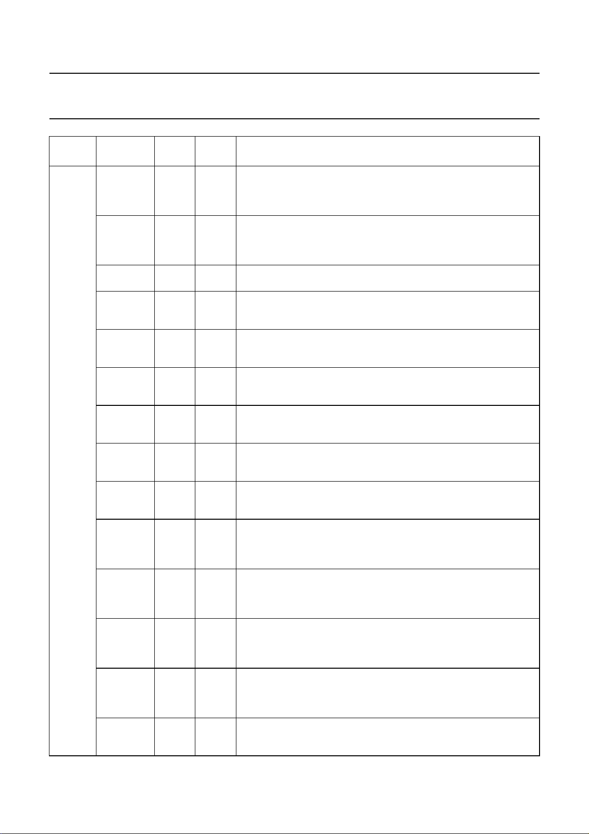
Philips Semiconductors Product specification
Multimedia bridge, high performance
SAA7146A
Scaler and PCI circuit (SPCI)
OFFSET
(HEX)
114 RPS_RE0 26 R RPS Task 0 Register access Error: this bit is set when the LDREG,
NAME BIT TYPE DESCRIPTION
STREG or MASKWRITE command tries to access a non-existing
register. This bit is reset by writing a logic 1 to the RPS_E0 bit in the ISR
or when a new RPS Task 0 is started.
RPS_PE0 25 R RPS Task 0 Page Error: this bit is set when the RPS Task 0 tries to
write-access an address outside the 4-kbyte page. This bit is reset by
writing a logic 1 to the RPS_E0 bit in the ISR or when a new RPS T ask0
is started.
RPS_A0 24 R RPS Task 0 Active: this bit is set whenever RPS Task 0 is executing
and not staying in a wait condition or uploading the working registers
DEBI_TO 23 R DEBI Time Out: this bit is set when the TIMEOUT value was reached.
This bit is reset by writing a logic 1 to the DEBI_E bit in the ISR. Reset
value is a logic 1.
DEBI_EF 22 R DEBI Format Error: this bit indicates an illegal command to immediate
transfer across a Dword boundary . This bit is reset by writing a logic 1 to
the DEBI_E bit in the ISR.
IIC_EA 21 R I
IIC_EW 20 R I
IIC_ER 19 R I
IIC_EL 18 R I
IIC_EF 17 R I
V3P 16 R Video DMA 3 Protection error: this bit is set when video DMA3
V2P 15 R Video DMA 2 Protection error: this bit is set when video DMA2
V1P 14 R Video DMA 1 Protection error: this bit is set when video DMA1
VF3 13 R Video FIFO 3 underflow/overflow: this bit is set when the video FIFO 3
2
C-bus Address Error: this bit is set when there is no acknowledge
after the device address. This bit is reset by writing a logic 1 to the IIC_E
bit in the ISR or when a new I2C-bus command starts.
2
C-bus Write data Error: this bit is set when there is no acknowledge
during the writing of the data byte(s). This bit is reset by writing a logic 1
to the IIC_E bit in the ISR or when a new I2C-bus command starts.
2
C-bus Read data Error This bit is set when there is no acknowledge
during reading of the data byte(s). This bit is reset by writing a logic 1 to
the IIC_E bit in the ISR or when a new I2C-bus command starts.
2
C-bus Loss arbitration Error: this bit is set when the I2C-bus loses its
arbitration. This bit is reset by writing a logic 1 to the IIC_E bit in the ISR
or when a new I2C-bus command starts.
2
C-bus Frame Error: this bit is set when there is an invalid
START/STOP condition since the last I2C-bus command. This bit is
reset by writing a logic 1 to the IIC_E bit in the ISR or when a new
I2C-bus command starts.
generates an address during an active transmission beyond its
protection address. This bit is reset by writing a logic 1 to the V_PE bit in
the ISR or by reloading the DMA base address.
generates an address during an active transmission beyond its
protection address. This bit is reset by writing a logic 1 to the V_PE bit in
the ISR or by reloading the DMA base address.
generates an address during an active transmission beyond its
protection address. This bit is reset by writing a logic 1 to the V_PE bit in
the ISR or by reloading the DMA base address.
has an overflow/underflow. This bit is reset when reloading the DMA
base address or by writing a logic 1 to the VFOU bit in the ISR.
1998 Apr 09 48
Page 49

Philips Semiconductors Product specification
Multimedia bridge, high performance
SAA7146A
Scaler and PCI circuit (SPCI)
OFFSET
(HEX)
114 VF2 12 R Video FIFO 2 underflow/overflow: this bit is set when the video FIFO 2
NAME BIT TYPE DESCRIPTION
has an overflow/underflow. This bit is reset when reloading the DMA
base address or by writing a logic 1 to the VFOU bit in the ISR.
VF1 11 R Video FIFO 1 overflow: this bit is set when the video FIFO 1 has an
overflow. This bit is reset when reloading the DMA base address or by
writing a logic 1 to the VFOU bit in the ISR.
AF2_in 10 R Audio input FIFO 2 underflow: this bit is set when the audio input
FIFO 2 has an underflow. This bit is reset by restarting the DMA channel
or by writing a logic 1 to the AFOU bit in the ISR.
AF2_out 9 R Audio output FIFO 2 overflow: this bit is set when the audio output
FIFO 2 has an overflow. This bit is reset by restarting the DMA channel
or by writing a logic 1 to the AFOU bit in the ISR.
AF1_in 8 R Audio input FIFO 1 underflow: this bit is set when the audio input
FIFO 1 has an underflow. This bit is reset by restarting the DMA channel
or by writing a logic 1 to the AFOU bit in the ISR.
AF1_out 7 R Audio output FIFO 1 overflow: this bit is set when the audio output
FIFO 1 has an overflow. This bit is reset by restarting the DMA channel
or by writing a logic 1 to the AFOU bit in the ISR.
− 6 − reserved
VGT 5 R Vertical Gate: this bit reflects the vertical gate at the HPS output
LNQG 4 R Line Qualifier Gate: this bit reflects the horizontal gate at the HPS
output
EC5S 3 R Event Counter 5 Status: this bit is set when the event counter 5
exceeds its threshold. This bit is reset by writing a logic 1 to the ECS bit
in the ISR.
EC4S 2 R Event Counter 4 Status: this bit is set when event counter 4 exceeds
its threshold. This bit is reset by writing a logic 1 to the ECS bit in the
ISR.
EC2S 1 R Event Counter 2 Status: this bit is set when event counter 2 exceeds
its threshold. This bit is reset by writing a logic 1 to the ECS bit in the
ISR.
EC1S 0 R Event Counter 1 Status: this bit is set when event counter 1 exceeds
its threshold. This bit is reset by writing a logic 1 to the ECS bit in the
ISR.
1998 Apr 09 49
Page 50
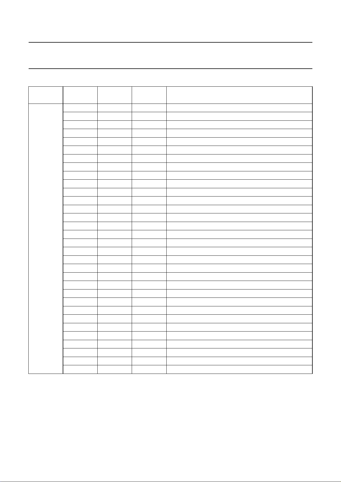
Philips Semiconductors Product specification
Multimedia bridge, high performance
Scaler and PCI circuit (SPCI)
Table 40 Interrupt enable register
OFFSET
(HEX)
DC PPEF 31 RW PCI Parity Error interrupt enable
NAME BIT TYPE DESCRIPTION
PABO 30 RW PCI Access Error interrupt enable
PPED 29 RW PCI Parity Errors on ‘real time Data’ interrupt enable
RPS_I1 28 RW enables interrupts issued by RPS commands in Task 1
RPS_I0 27 RW enables interrupts issued by RPS commands in Task 0
RPS_late1 26 RW RPS Task 1 late interrupt enable
RPS_late0 25 RW RPS Task 0 late interrupt enable
RPS_E1 24 RW RPS_Error1 interrupt enable
RPS_E0 23 RW RPS_Error0 interrupt enable
RPS_TO1 22 RW RPS time out Task 1 interrupt enable
RPS_TO0 21 RW RPS time out Task 0 interrupt enable
UPLD 20 RW RPS Upload interrupt enable
DEBI_S 19 RW DEBI Status interrupt enable
DEBI_E 18 RW DEBI Error interrupt enable
IIC_S 17 RW I
IIC_E 16 RW I
A2_in 15 RW Audio input DMA2 protection interrupt enable
A2_out 14 RW Audio output DMA2 protection interrupt enable
A1_in 13 RW Audio input DMA1 protection interrupt enable
A1_out 12 RW Audio output DMA1 protection interrupt enable
AFOU 11 RW Audio FIFO Overflow/Underflow interrupt enable
V_PE 10 RW Video address Protection Error interrupt enable
VFOU 9 RW Video FIFO Overflow/Underflow interrupt enable
FIDA 8 RW Field ID port A interrupt enable
FIDB 7 RW Field ID port B interrupt enable
PIN3 6 RW GPIO Pin 3 interrupt enable
PIN2 5 RW GPIO Pin 2 interrupt enable
PIN1 4 RW GPIO Pin 1 interrupt enable
PIN0 3 RW GPIO Pin 0 interrupt enable
ECS 2 RW Event Counter 1, 2, 4 and 5 Status interrupt enable
EC3S 1 RW Event Counter 3 Status interrupt enable
EC0S 0 RW Event Counter 0 Status interrupt enable
2
C Status interrupt enable
2
C Error interrupt enable
SAA7146A
1998 Apr 09 50
Page 51
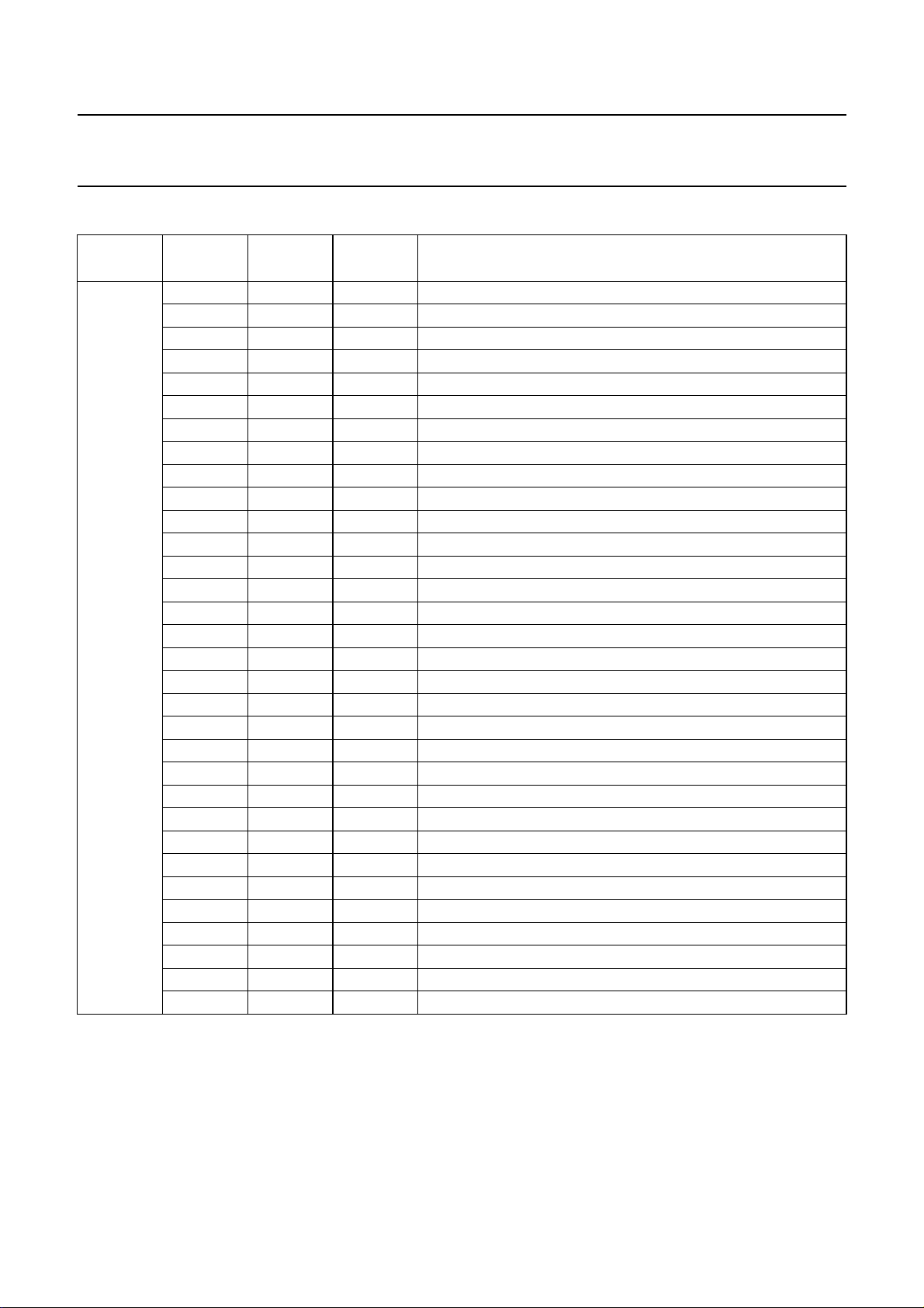
Philips Semiconductors Product specification
Multimedia bridge, high performance
Scaler and PCI circuit (SPCI)
Table 41 Interrupt status register
OFFSET
(HEX)
10C PPEF 31 RW PCI Parity Error interrupt status
NAME BIT TYPE DESCRIPTION
PABO 30 RW PCI Access Error interrupt status
PPED 29 RW PCI Parity Errors on ‘real time Data’ interrupt status
RPS_I1 28 RW interrupt issued by RPS command from Task 1 interrupt status
RPS_I0 27 RW interrupt issued by RPS command from Task 0 interrupt status
RPS_late1 26 RW RPS Task 1 is late interrupt status
RPS_late0 25 RW RPS Task 0 is late interrupt status
RPS_E1 24 RW RPS_Error from Task 1 interrupt status
RPS_E0 23 RW RPS_Error from Task 0 interrupt status
RPS_TO1 22 RW RPS time out Task 1 interrupt status
RPS_TO0 21 RW RPS time out Task 0 interrupt status
UPLD 20 RW RPS Upload interrupt status
DEBI_S 19 RW DEBI Status interrupt status
DEBI_E 18 RW DEBI Error interrupt status
IIC_S 17 RW I
IIC_E 16 RW I
A2_in 15 RW Audio input DMA2 protection interrupt status
A2_out 14 RW Audio output DMA2 protection interrupt status
A1_in 13 RW Audio input DMA1 protection interrupt status
A1_out 12 RW Audio output DMA1 protection interrupt status
AFOU 11 RW Audio FIFO Overflow/Underflow interrupt status
V_PE 10 RW Video address Protection Error interrupt status
VFOU 9 RW Video FIFO Overflow/Underflow interrupt status
FIDA 8 RW Field ID port A interrupt status
FIDB 7 RW Field ID port B interrupt status
PIN3 6 RW GPIO Pin 3 interrupt status
PIN2 5 RW GPIO Pin 2 interrupt status
PIN1 4 RW GPIO Pin 1 interrupt status
PIN0 3 RW GPIO Pin 0 interrupt status
ECS 2 RW Event Counter 1, 2, 4 and 5 interrupt status
EC3S 1 RW Event Counter 3 interrupt status
EC0S 0 RW Event Counter 0 interrupt status
2
C Status interrupt status
2
C Error interrupt status
SAA7146A
1998 Apr 09 51
Page 52
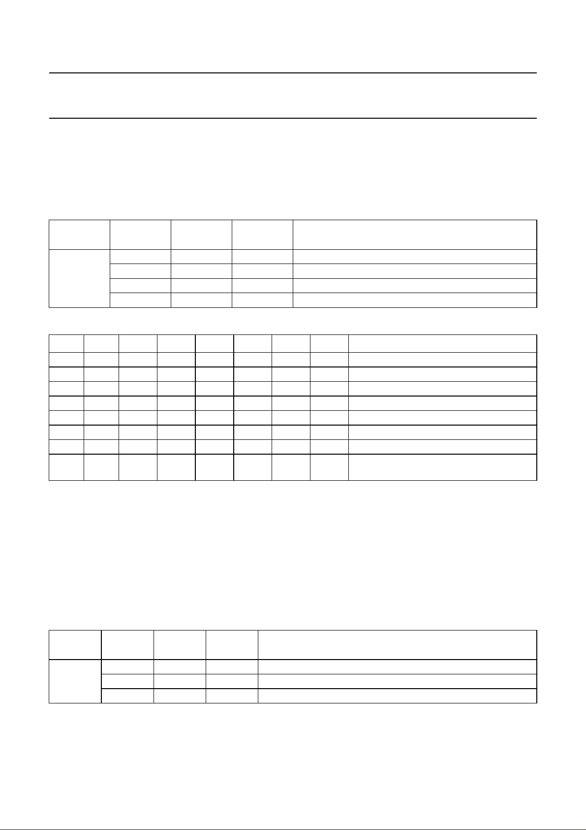
Philips Semiconductors Product specification
Multimedia bridge, high performance
SAA7146A
Scaler and PCI circuit (SPCI)
7.6 General Purpose Inputs/Outputs (GPIO)
7.6.1 G
The SAA7146A has four general purpose I/O pins. For example, they could be used to signal to other devices a
power-down mode or to map an internal status bit to it, e.g. to detect a sync lost from the VBLK pin of the SAA7110.
Table 42 GPIO registers
OFFSET
Table 43 GPIO control register
BIT 7 BIT 6 BIT 5 BIT 4 BIT 3 BIT 2 BIT 1 BIT 0 DESCRIPTION
0000XXXXinput, no interrupt condition
0001XXXXinput, rising edge is interrupt condition
0010XXXXinput, falling edge is interrupt condition
0011XXXXinput, both edges are interrupt condition
01X0XXXXoutput, fixed constant LOW
01X1XXXXoutput, fixed constant HIGH
10XXXXXXreserved
1 1 SBA[5] SBA[4] SBA[3] SBA[2] SBA[1] SBA[0] output, monitoring the selected status bits of
ENERAL
(HEX)
E0 GPIO3 31 to 24 RW GPIO3 control register
NAME BIT TYPE DESCRIPTION
GPIO2 23 to 16 RW GPIO2 control register
GPIO1 15 to 8 RW GPIO1 control register
GPIO0 7 to 0 RW GPIO0 control register
PSR or SSR; see Table 48
7.7 Event counter
The event counters in the SAA7146A provide the possibility of obtaining a statistical look at the different interrupt sources.
For this purpose six counters are implemented in two registers (EC1R and EC2R). Each register contains one 12-bit
counter and two 10-bit counters. To be flexible in the information collected in the counters it is possible to map each
status bit to any counter. This is done via the Event Counter Source Select Register (ECSSR). The four 10-bit counters
and the two 12-bit counters are able to select one of the 64 possible sources (see Table 47). In addition to the counting,
it is possible to generate interrupts via threshold values for the counters. These thresholds are kept in the two Event
Threshold Registers (ET1R and ET2R). If a counter exceeds its threshold, it is reset to zero and the corresponding status
bit is set.
Table 44 Event Counter set 1 Register (EC1R)
OFFSET
(HEX)
118 EC2 [9:0] 31 to 22 R Event Counter Two: this is the second 10-bit counter
1998 Apr 09 52
NAME BIT TYPE DESCRIPTION
EC1 [9:0] 21 to 12 R Event Counter One: this is the first 10-bit counter
EC0 [1:0] 11 to 0 R Event Counter Zero: this is the first 12-bit counter
Page 53
Philips Semiconductors Product specification
Multimedia bridge, high performance
Scaler and PCI circuit (SPCI)
Table 45 Event Counter set 2 Register (EC2R)
OFFSET
(HEX)
11C EC5 [9:0] 31 to 22 R Event Counter Five: this is the fourth 10-bit counter
Table 46 Event Counter set 1 Source Select Register 1 (EC1SSR)
OFFSET
(HEX)
E4 − 31 to 24 − reserved
NAME BIT TYPE DESCRIPTION
EC4 [9:0] 21 to 12 R Event Counter Four: this is the third 10-bit counter
EC3 [11:0] 11 to 0 R Event Counter Three: this is the second 12-bit counter
NAME BIT TYPE DESCRIPTION
ECS2 [5:0] 23 to 18 RW Event Counter 2 Source: this 6 bit value addresses one of the status bits
ECEN2 17 RW Event Counter 2 Enable: if this bit is set, event counter 2 is enabled
ECCLR2 16 RW Event Counter 2 Clear: writing a logic 1 to this bit will clear event counter 2
ECS1 [5:0] 15 to 10 RW Event Counter 1 Source: this 6 bit value addresses one of the status bits
ECEN1 9 RW Event Counter 1 Enable: if this bit is set event counter 1 is enabled
ECCLR1 8 RW Event Counter 1 Clear: writing a logic 1 to this bit will clear event counter 1
ECS0 [5:0] 7 to 2 RW Event Counter 0 Source: this 6 bit value addresses one of the status bits
ECEN0 1 RW Event Counter 0 Enable: if this bit is set event counter 0 is enabled
ECCLR0 0 RW Event Counter 0 Clear: writing a logic 1 to this bit will clear event counter 0
SAA7146A
Table 47 Event Counter set 2 Source Select Register (EC2SSR)
OFFSET
(HEX)
E8 − 31 to 24 − reserved
Table 48 Status Bit Addresses (SBA)
ADDRESS
(HEX)
00 PPEF number of PCI Parity errors
01 PABO number of PCI Access errors
02 PPED every PCI clock cycle with ‘data’ parity error
03 RPS_I1 number of RPS interrupts Task 1
NAME BIT TYPE DESCRIPTION
ECS5 [5:0] 23 to 18 RW Event Counter 5 Source: this 6 bit value addresses one of the status bits
ECEN5 17 RW Event Counter 5 Enable: if this bit is set the event counter 5 is enabled
ECCLR5 16 RW Event Counter 5 Clear: writing a logic 1 to this bit will clear event counter 5
ECS4 [5:0] 15 to 10 RW Event Counter 4 Source: this 6 bit value addresses one of the status bits
ECEN4 9 RW Event Counter 4 Enable: if this bit is set event counter 4 is enabled
ECCLR4 8 RW Event Counter 4 Clear: writing a logic 1 to this bit will clear event counter 4
ECS3 [5:0] 7 to 2 RW Event Counter 3 Source: this 6 bit value addresses one of the status bits
ECEN3 1 RW Event Counter 3 Enable: if this bit is set event counter 3 is enabled
ECCLR3 0 RW Event Counter 3 Clear: writing a logic 1 to this bit will clear event counter 3
STATUS BIT EVENTS TO BE COUNTED
1998 Apr 09 53
Page 54

Philips Semiconductors Product specification
Multimedia bridge, high performance
SAA7146A
Scaler and PCI circuit (SPCI)
ADDRESS
(HEX)
04 RPS_I0 number of RPS interrupts Task 0
05 RPS_LATE1 number of RPS late errors for Task 1
06 RPS_LATE0 number of RPS late errors for Task 0
07 RPS_E1 number of RPS errors for Task 1
08 RPS_E0 number of RPS errors for Task 0
09 RPS_TO1 number of time outs for RPS Task 1
0A RPS_TO0 number of time outs for RPS Task 0
0B UPLD time for upload, in PCI clocks
0C DEBI_S time DEBI is busy, in PCI clocks
0D DEBI_E number of DEBI events in total
0E IIC_S time I
0F IIC_E number of I
10 A2_in number of protection hits
11 A2_out number of protection hits
12 A1_in number of protection hits
13 A1_out number of protection hits
14 AFOU number of audio FIFOs overflows/underflows in total
15 V_PE number of video FIFO protection violations in total
16 VFOU number of video FIFOs overflows/underflows in total
17 FIDA number of odd/even fields on port A (defined via FIDESA)
18 FIDB number of odd/even fields on port B (defined via FIDESB)
19 PIN3 number of active edges as defined in the GPIO registers; see Table 43
1A PIN2 number of active edges as defined in the GPIO registers; see Table43
1B PIN1 number of active edges as defined in the GPIO registers; see Table43
1C PIN0 number of active edges as defined in the GPIO registers; see Table 43
1D ECS number of threshold overflows from EC1, EC2, EC4 and EC5 in total
1E EC3S number of threshold overflows of EC3S
1F EC0S number of threshold overflows of EC0S
20 PRQ time from REQ# to GNT#, in PCI clocks
21 PMA time in active master mode, in PCI clocks
22 RPS_RE1 number of RPS register access errors for Task 1
23 RPS_PE1 number of page errors for RPS Task 1
24 RPS_A1 time of RPS Task 1 busy, in PCI clocks
25 RPS_RE0 number of RPS register access errors for Task 0
26 RPS_PE0 number of page errors for RPS Task 0
27 RPS_A0 time of RPS Task 0 busy, in PCI clocks
28 DEBI_TO number of DEBI time out events
29 DEBI_EF number of format errors on DEBI port
2A IIC_EA number of address errors on the I
2B IIC_EW number of I
STATUS BIT EVENTS TO BE COUNTED
2
C-bus is busy, in PCI clocks
2
C-bus errors in total
2
C-bus
2
C-bus write data errors
1998 Apr 09 54
Page 55
Philips Semiconductors Product specification
Multimedia bridge, high performance
Scaler and PCI circuit (SPCI)
ADDRESS
(HEX)
2C IIC_ER number of I
2D IIC_EL number of arbitration losses on the I
2E IIC_EF number of I
2F V3P number of protection violations for video FIFO 3
30 V2P number of protection violations for video FIFO 2
31 V1P number of protection violations for video FIFO 1
32 VF3 number of missed Dwords
33 VF2 number of missed Dwords
34 VF1 number of missed Dwords
35 AF2_in number of missed Dwords
36 AF2_out number of missed Dwords
37 AF1_in number of missed Dwords
38 AF1_out number of missed Dwords
39 − reserved
3A VGT number of V_syncs in acquisition of HPS
3B LNQG number of output lines
3C EC5S number of threshold overflows of EC5
3D EC4S number of threshold overflows of EC4
3E EC2S number of threshold overflows of EC2
3F EC1S number of threshold overflows of EC1
STATUS BIT EVENTS TO BE COUNTED
2
C-bus read data errors
2
C-bus
2
C-bus frame errors
SAA7146A
Table 49 Event Counter Threshold set 1 Register (ECT1R)
OFFSET
(HEX)
EC ECT2 [9:0] 31 to 22 RW Event Counter 2 Threshold: this is the threshold for the
Note
1. Each of these threshold values shows the limit up to which the related counter will run before it sets its interrupt status
bit.
NAME BIT TYPE DESCRIPTION
second 10-bit counter; see note 1
ECT1 [9:0] 21 to 12 RW Event Counter 1 Threshold: this is the threshold for the first
10-bit counter; see note 1
ECT0 [11:0] 11 to 0 RW Event Counter 0 Threshold: this is the threshold for the first
12-bit counter; see note 1
1998 Apr 09 55
Page 56
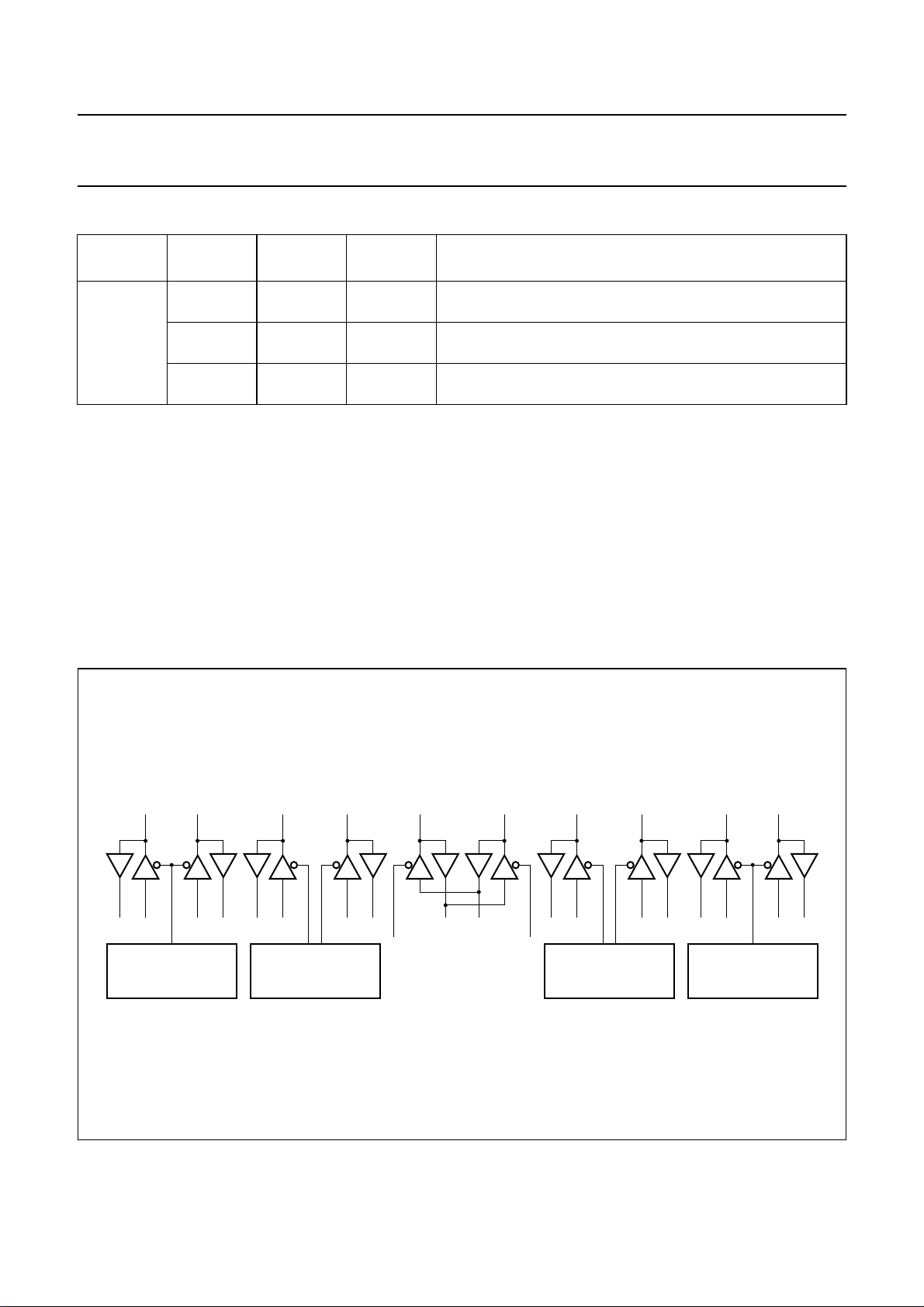
Philips Semiconductors Product specification
Multimedia bridge, high performance
SAA7146A
Scaler and PCI circuit (SPCI)
Table 50 Event Counter Threshold set 2 Register (ECT2R)
OFFSET
(HEX)
F0 ECT6 [9:0] 31 to 22 RW Event Counter 5 Threshold: this is the threshold for the
Note
1. Each of these threshold values shows the limit up to which the related counter will run before it sets it interrupt status
bit.
7.8 Video processing
7.8.1 T
The real time video interface consists of two bidirectional 8-bit wide ports transporting colour difference samples and
luminance samples in a byte sequential manner. Each of the two video ports (A and B) has its own clock pin, pixel
qualifier and horizontal and vertical sync signal pin. The sync signal can be optionally coded in SAV and EAV codes
according to the D1 standard (SMPTE125M or CCIR 656). The two 8-bit ports can be combined to form a single 16-bit
wide YUV port to be compatible to the DMSD2 output format.
NAME BIT TYPE DESCRIPTION
fourth 10-bit counter; see note 1
ECT5 [9:0] 21 to 12 RW Event Counter 4 Threshold: this is the threshold for the third
10-bit counter; see note 1
ECT4 [11:0] 11 to 0 RW Event Counter 3 Threshold: this is the threshold for the
second 12-bit counter; see note 1
HE REAL TIME VIDEO INTERFACE
D1_A
handbook, full pagewidth
VIDEO DATA STREAM
PXQ_A HS_A VS_A LLC_A LLC_B VS_B HS_B PXQ_B D1_B
INITIAL SETTINGS OF
HANDLING
VID_a
56H
DUAL D1 INTERFACE
SIO_a
52H
Fig.8 The real time video interface.
1998 Apr 09 56
INITIAL SETTINGS OF
DUAL D1 INTERFACE
SIO_b
50H
VIDEO DATA STREAM
HANDLING
VID_b
54H
MHB049
Page 57
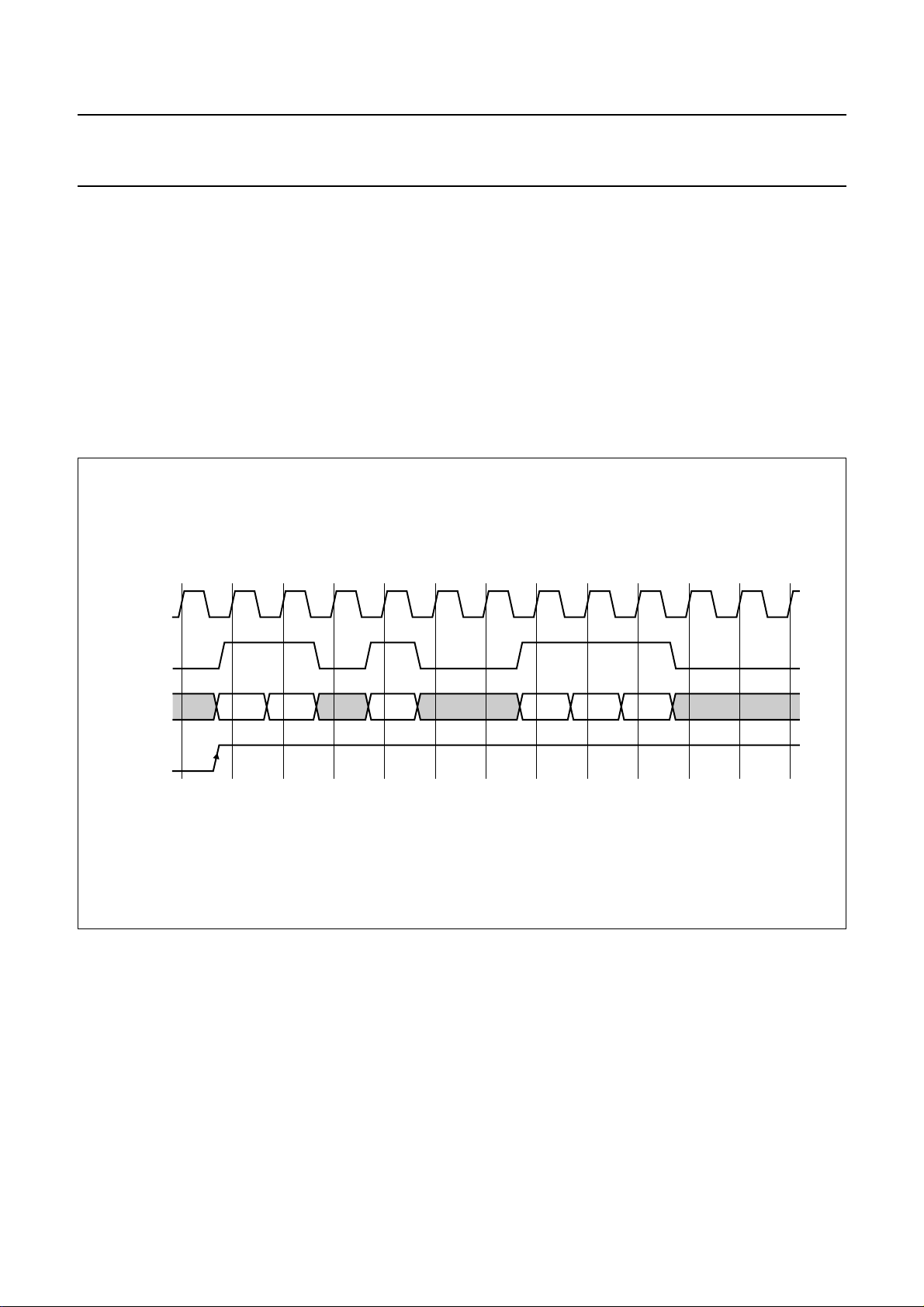
Philips Semiconductors Product specification
Multimedia bridge, high performance
SAA7146A
Scaler and PCI circuit (SPCI)
7.8.2 DD1: DUAL D1 (CCIR 656, SMPTE125M), I/O
7.8.2.1 Cb-Y-Cr-Y 8-bit wide stream
In this mode two video ports with YUV 4 :2:2 sampling scheme are available. Each D1 port has an I/O capability and
has a separate clock input and separate sync lines. In this format the pixel rate is equivalent to the clock rate LLC.
The colour difference signal sample and luminance signal sample (straight binary) are byte-wise multiplexed into the
same 8-bit wide data stream, with sequence and timing in accordance with CCIR 656 recommendation (respectively
according to D1 for 60 Hz application). The incoming and scaled data are reformatted to 16-bit for the HPS data path and
the corresponding reference signals are generated. A discontinuous data stream is supported by accepting or generating
a pixel/byte qualifying signal (PXQ = 1: qualified pixel, PXQ = 0: invalid data, see Fig.9). The start condition for
synchronizing to the correct Cb-Y-Cr-Y sequence is given by the selected horizontal reference signal. The sequence
increments only with qualified bytes.
handbook, full pagewidth
LLC_x
PXQ_x
D1_x (7 to 0)
HS_x
CrYCb Y Cb Y
MHB050
Fig.9 Timing of PXQ_x for serial 8-bit data input at the D1_x port.
1998 Apr 09 57
Page 58
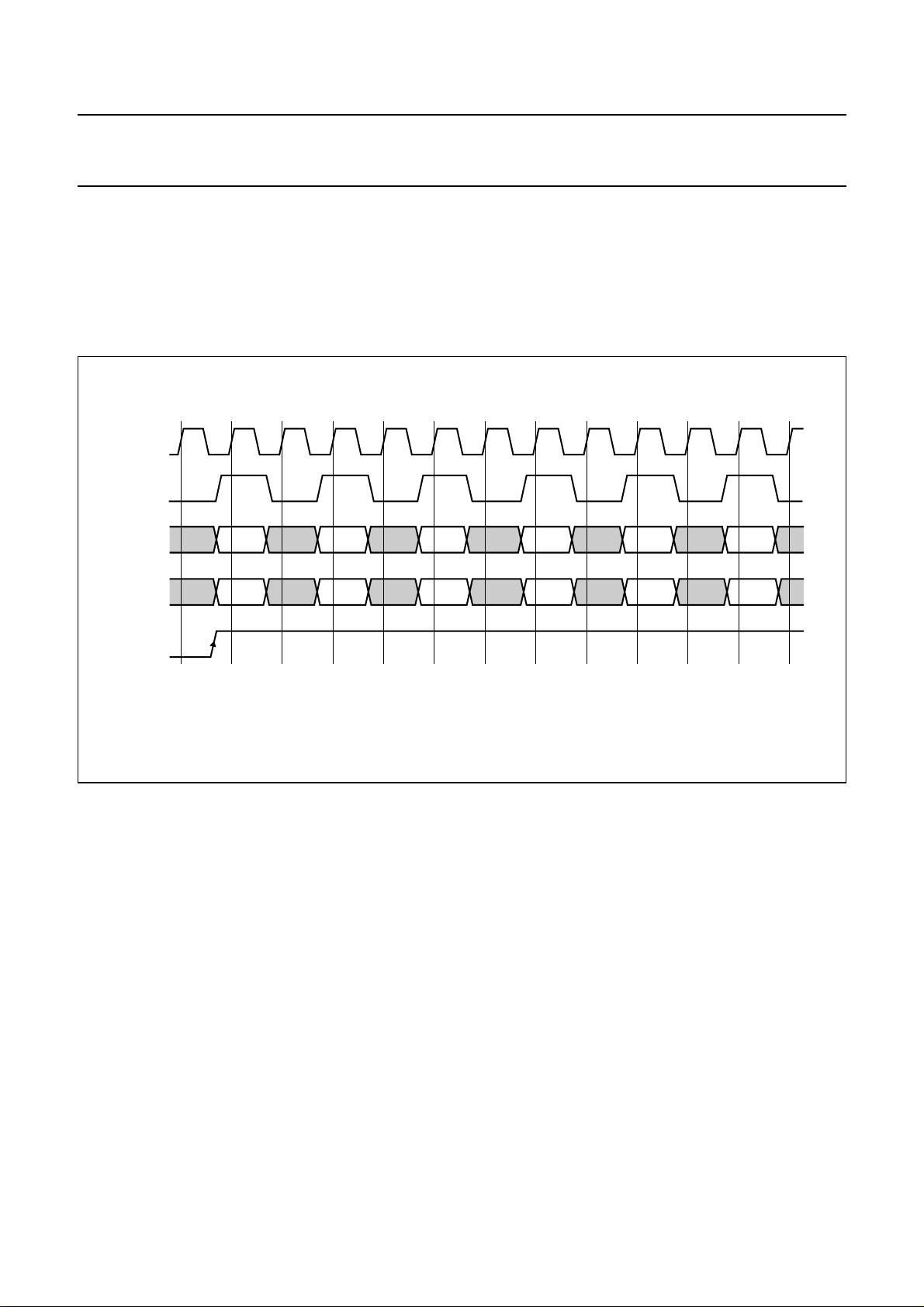
Philips Semiconductors Product specification
Multimedia bridge, high performance
SAA7146A
Scaler and PCI circuit (SPCI)
7.8.2.2 YUV 16-bit parallel (DMSD2) stream
In this mode only the HPS data path is available since the BRS data path supports only 8-bit wide data streams. Colour
difference signal and luminance signal (straight binary) are available in parallel on a 16-bit wide data stream. In this mode
both D1 ports are inputs (see Fig.10). With this format the pixel rate is half the clock rate LLC. The start condition for
synchronising the clock divider and/or the correct U-V sequence is given by the CREF signal, which must be connected
to the same port as the colour difference signal.
handbook, full pagewidth
LLC
PXQ_A
(CREF)
D1_A (7 to 0) Cr0
D1_B (7 to 0)
Cb0
Y0
Cr2
Y2 Y4 Y5Y1
Y3
Cb4 Cr4Cb2
HS_x
MHB051
Fig.10 Timing of PXQ_x for 16-bit data input at the D1_x port.
7.8.3 V
IDEO DATA FORMATS ON DD1
D1 (SMPTE125M, CCIR 656) as well as YUV16 represent both the same 4 :2:2 sample scheme. Both formats,
D1 and YUV16, are assumed to agree with the CCIR recommendation 601 coding:
Y = 16 = black, 0%
Y = 235 = white, 100% brightness
U,V = 128 = no colour, 0% saturation
U,V = 128 ±112 = full colour, 100% saturation.
Data path processing in HPS and BRS is not limited to this range and allows overshoots and uses ‘margins’ for
processing. The reference values can be manipulated by the BCS processing in the HPS data path.
7.8.4 V
IDEO TIMING REFERENCE CODES (SAVAND EAV)
There are two timing reference codes; one at the beginning of each video data block [Start of Active Video (SAV)] and
one at the end of each video data block [End of Active Video (EAV)] as shown in Fig.11.
Each timing reference code consists of a four byte sequence in the following format: FF 00 00 XY. (values are expressed
in hexadecimal notation: codes FF, 00 are reserved for use in timing reference codes). The first three bytes are a fixed
preamble. The fourth byte contains information defining field identification, the state of field blanking and the state of line
blanking. The assignment of bits within the timing reference code is given in Table 51.
1998 Apr 09 58
Page 59
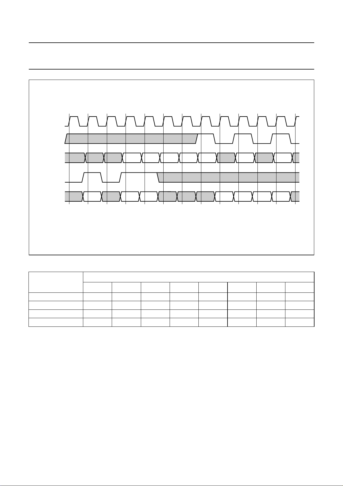
Philips Semiconductors Product specification
Multimedia bridge, high performance
Scaler and PCI circuit (SPCI)
handbook, full pagewidth
LLC
PXQ_x
D1_x (7 to 0) FFH
PXQ_x
D1_x (7 to 0)
Y Y FFH 00H 00H EAVCr
00H SAV Cb Y Cr00H
SAA7146A
MHB052
Fig.11 Timing of PXQ_x for CCIR 656 at the D1_x port.
Table 51 Video timing reference codes
BIT NUMBER
BYTE
7 (MSB) 6 5 4 3 2 1 0 (LSB)
First 1 1 1 1 1 1 1 1
Second 0 0 0 0 0 0 0 0
Third 0 0 0 0 0 0 0 0
Fourth 1 F
(1)
(2)
V
(3)
H
(4)
P
3
(4)
P
2
(4)
P
1
(4)
P
0
Notes
1. F = logic 0 during field 1 and logic 1 during field 2.
2. V = logic 0 elsewhere and logic 1 during field blanking.
3. H = logic 0 in SAV and logic 1 in EAV.
4. P
0,P1,P2
and P3: protection bits (see Table 52).
Bits P0,P1,P2and P3, have states dependent on the states of the bits F, V and H as shown in Table 52. At the receiver
(SAA7146A) this arrangement permits one-bit errors to be corrected. If two-bit errors or up to four-bit errors occur, i. e.
depending on uncoded protection bits, the circuit processes direct on the coded values. In this case the protection bits
are ignored.
SAV and EAV are only decoded and removed from the signal stream (substituted with neighbouring first or last active
video sample), if chosen this way. However, ‘single’ qualified codes of ‘00’ and/or ‘FF’ in the data stream, remain in the
data stream and are processed as data.
1998 Apr 09 59
Page 60
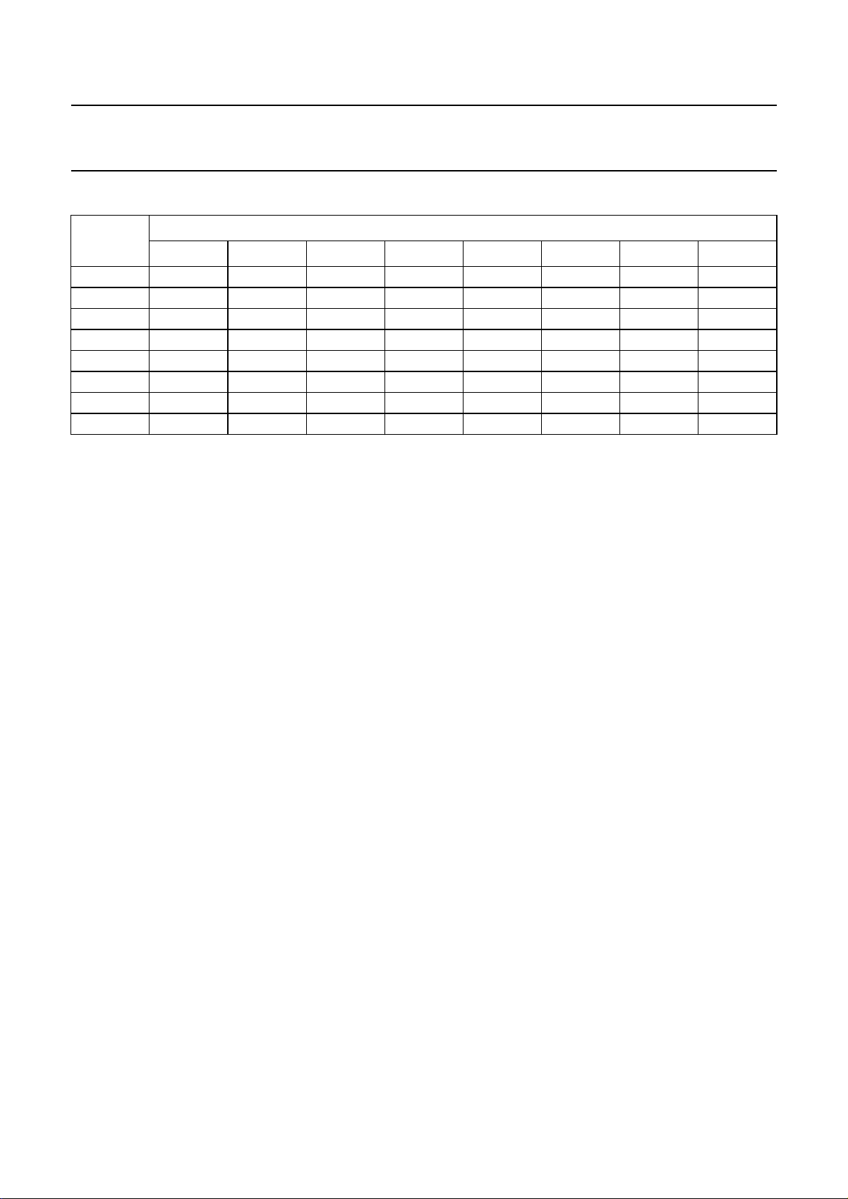
Philips Semiconductors Product specification
Multimedia bridge, high performance
SAA7146A
Scaler and PCI circuit (SPCI)
Table 52 Protection bits
BIT
NUMBER
711111111
600001101
500110011
401010101
301100110
201011010
100111100
001101001
7.8.5 SYNCHRONIZATION SIGNALS
Horizontal, vertical and frame synchronization signals are
either carried beside the data stream on the extra sync
pins of DD1 (one pair of sync pins per D1 channel) or are
encoded as SAV and EAV in the 8-bit wide video signal
stream. For the 16-bit wide YUV stream sync signals are
always available on separate pins. For D1 video inputs the
SAA7146A is programmed to determine where to recover
the synchronization information (from the dedicated sync
pins or from the encoded SAV and EAV codes in the data
stream).
For D1 video outputs, the SAA7146A can be programmed
to deliver synchronization information both in SAV and
EAV codes as well as on the dedicated sync pins.
Non-standard rastered video signals are supported by
sync signals at the dedicated sync pins as well as via SAV
and EAV codes. The number of clock cycles, pixels per
line and lines per field can be non-standard. These number
can range from 1 up to 4095.
The signal at the HS pin can perform the following
functions:
• HS: input only, the rising edge is selected to act as
timing reference
• HREF: input only, gated with CREF, the rising edge is
selected as timing reference
• HGT: I/O, HIGH during active video
• ACT input only: HIGH during active video, inactive
during horizontal and vertical blanking
• HGT and ACT: envelope all active pixels (there is no
active pixel outside HGT or ACT), but may also include
clock cycles marked as not valid pixels by means of
PXQ.
FIXED 1 F V H P
FUNCTION
3
The vertical sync signal can perform the following
functions:
• VS: input only positive or negative, one edge is selected
as timing reference:
– If selected edge of VS and selected edge of HS are
in phase, then begin 1st (odd) field
– If selected edges of VS and HS are out of phase, then
begin 2nd (even) field.
• V-DMSD: input only, falling (trailing) edge is timing
reference:
– If falling edge of V-DMSD is in high phase of HREF,
then begin 1st (odd) field
– If falling edge of V-DMSD is in low phase of HREF,
then begin 2nd (even) field.
• VGT: I/O, HIGH during active video, (no holes for
horizontal blanking)
• FS: input only, positive or negative, frame sync,
(odd/even), (313/312, 263/262 lines) HIGH in one field,
LOW in the other, changes on full line boundaries only.
7.8.6 F
The fields are detected simultaneously at both D1 sync
inputs. The results are available in two status registers.
IELD DETECTION
P
2
P
1
P
0
1998 Apr 09 60
Page 61
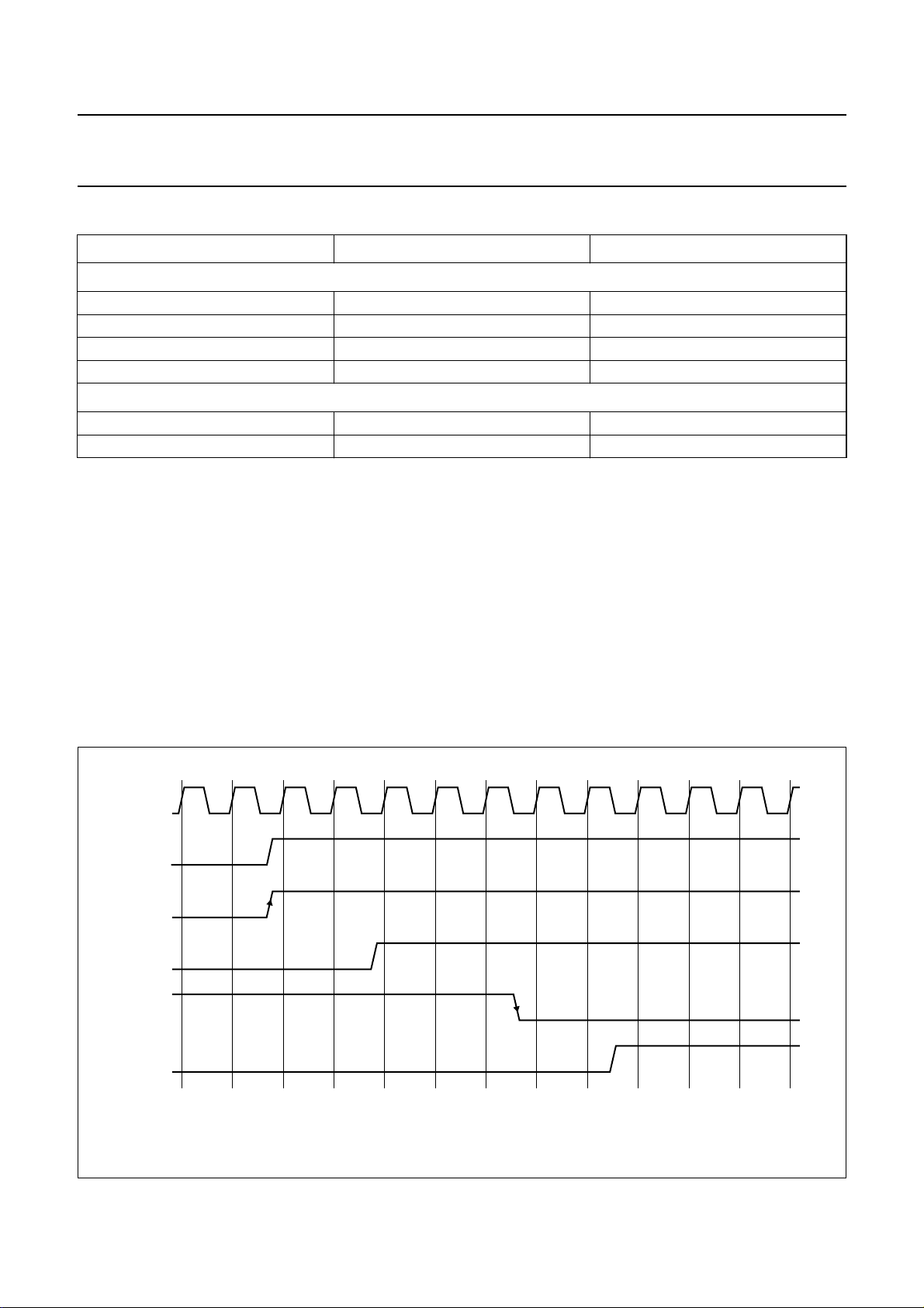
Philips Semiconductors Product specification
Multimedia bridge, high performance
SAA7146A
Scaler and PCI circuit (SPCI)
Table 53 Field interval definitions for D1 (CCIR 656) SAV and EAV codes; note 1
DEFINITION 625 LINES 525 LINES
V-digital field blanking
Field 1; start (V = 1) Line 624 Line 1
Field 1; finish (V = 0) Line 23 Line 10
Field 2; start (V = 1) Line 311 Line 264
Field 2; finish (V = 0) Line 336 Line 273
F-digital field identification
Field 1; F = 0 Line 1 Line 4
Field 2; F = 1 Line 313 Line266
Note
1. Signals F and V change state synchronously with the end of active video timing reference code at the beginning of
the digital line.
7.8.6.1 Field detection control
Field detection modes:
• Direct mode: FLD signal detected from incoming H/V signals, for timing behaviour see Fig.11.
• Forced toggle: FLD signal regularly synchronized to source, but will never stay more than two fields with the same ID.
The circuit expects to detect a field change with every vertical reference edge, if the field does not change (field error),
the circuit change the field ID automatically. If the circuit switch to the wrong sequence i. e. at the beginning of
processing, it will be synchronized after one second where no field error has occurred.
• Free toggle: FLD signal toggles with every vertical reference edge, independent of source FID.
handbook, full pagewidth
LLC
HS
VS
FLD
V-DMSD
FLD-DMSD
Fig.12 Timing of field detection EVEN-to-ODD for direct mode.
1998 Apr 09 61
MHB053
Page 62
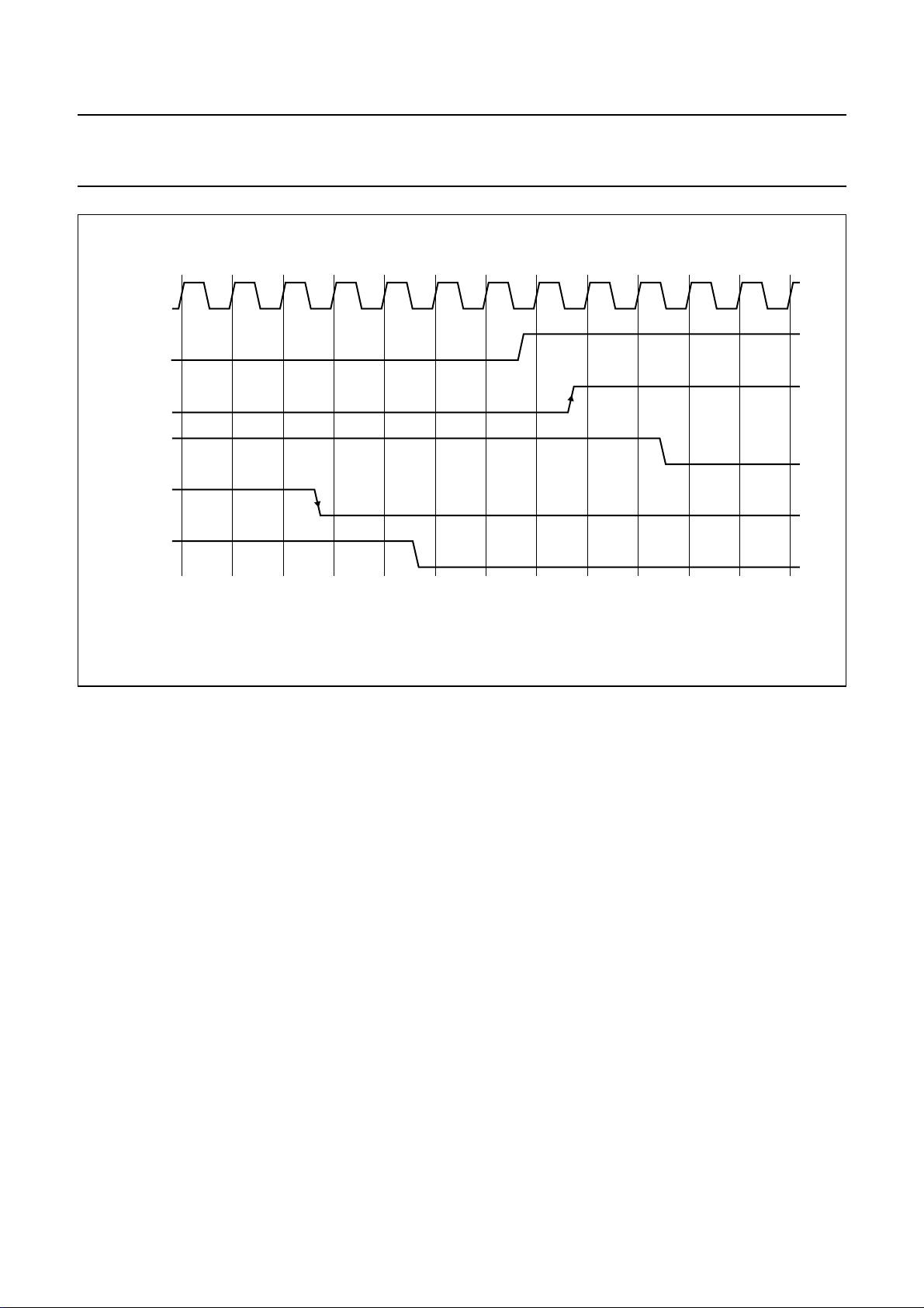
Philips Semiconductors Product specification
Multimedia bridge, high performance
Scaler and PCI circuit (SPCI)
handbook, full pagewidth
LLC
HS
VS
FLD
V-DMSD
FLD-DMSD
SAA7146A
MHB054
Fig.13 Timing of field detection ODD-to-EVEN for direct mode.
7.8.7 ACQUISITION CONTROL
The processing window for the scaling unit is defined in the acquisition control. The internal counters (one for the HPS
and one for the BRS) receives programmable values for offset (HXO11 to HXO0, HYO11 to HYO0 and BXO9 to BXO0,
BYO9 to BYO0) and length (NumLines, NumBytes). These counters are reset by the corresponding sync reference input
signal. The horizontal counter increments in qualified pixels for the HPS and qualified bytes for the BRS, the vertical
counter increments in qualified lines, i.e. lines containing at least one qualified pixel. In order to avoid programming
dependent line drop effects, the horizontal offset value must not exceed the number of pixels per line. In order to avoid
programming dependent field drop effects, the vertical offset value must not exceed the number of lines per field.
The acquisition provides the possibility to re-program the vertical offset after the previous job is done (EOW at the
HPS and BRS is reached). Thus multiple windows can be opened during one field.
1998 Apr 09 62
Page 63
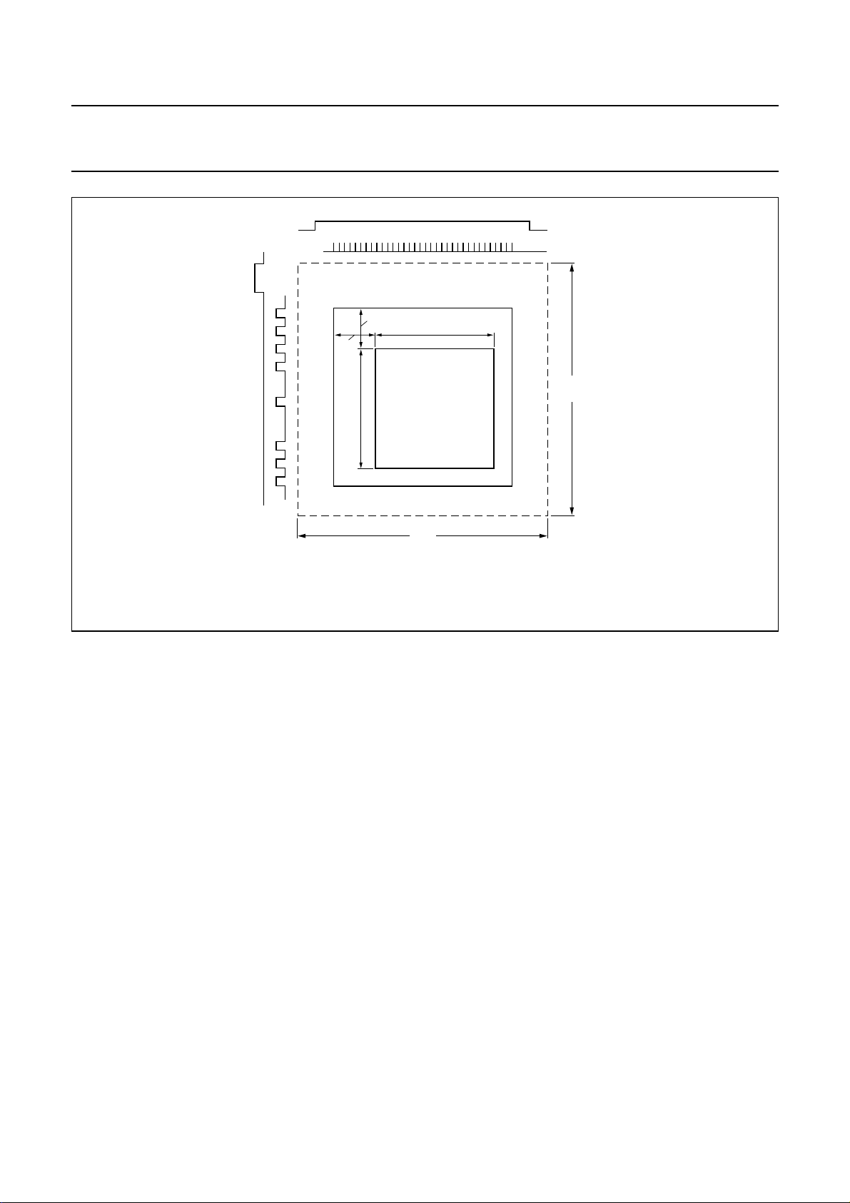
Philips Semiconductors Product specification
Multimedia bridge, high performance
Scaler and PCI circuit (SPCI)
handbook, full pagewidth
VS_x
(1)
LQ
ACTIVE VIDEO WINDOW
HYO
HXO
BXO
NumLines
BYO
NumBytes
SCALING
WINDOW
line
SAA7146A
HS_x
PXQ_x
field/
frame
MHB055
(1) LQ = qualified lines, i.e. lines containing at least one qualified pixel.
Fig.14 Reference signals for scaling window.
7.8.8 COMPARISON BETWEEN CCIR 656 LINE AND SOURCE LINE COUNTER
This section describes how to choose the vertical offset and how to use the source line counter event for RPS
programming for capturing the expected line.
The internal Source Line Counter (SLC) is reset by the selected edge of the vertical sync signal which is provided at port
VS_x. The falling and rising edges of this signal are selected by the SYNC_X bits in the ‘Initial settings DD1 Port Register’
(offset = 50H). Consequently, the behaviour of the SLC depends on the connected vertical sync signal so that different
offsets must be selected to capture the expected line. The active video begins in the CCIR 656 line 23 of the video signal;
Table 54 lists the different offsets which must be selected to capture the expected line. The subsequent diagrams and
tables illustrate the relationship between the different vertical sync signals of the PAL and NTSC standards, the ODD and
EVEN field and the internal SLC.
1998 Apr 09 63
Page 64
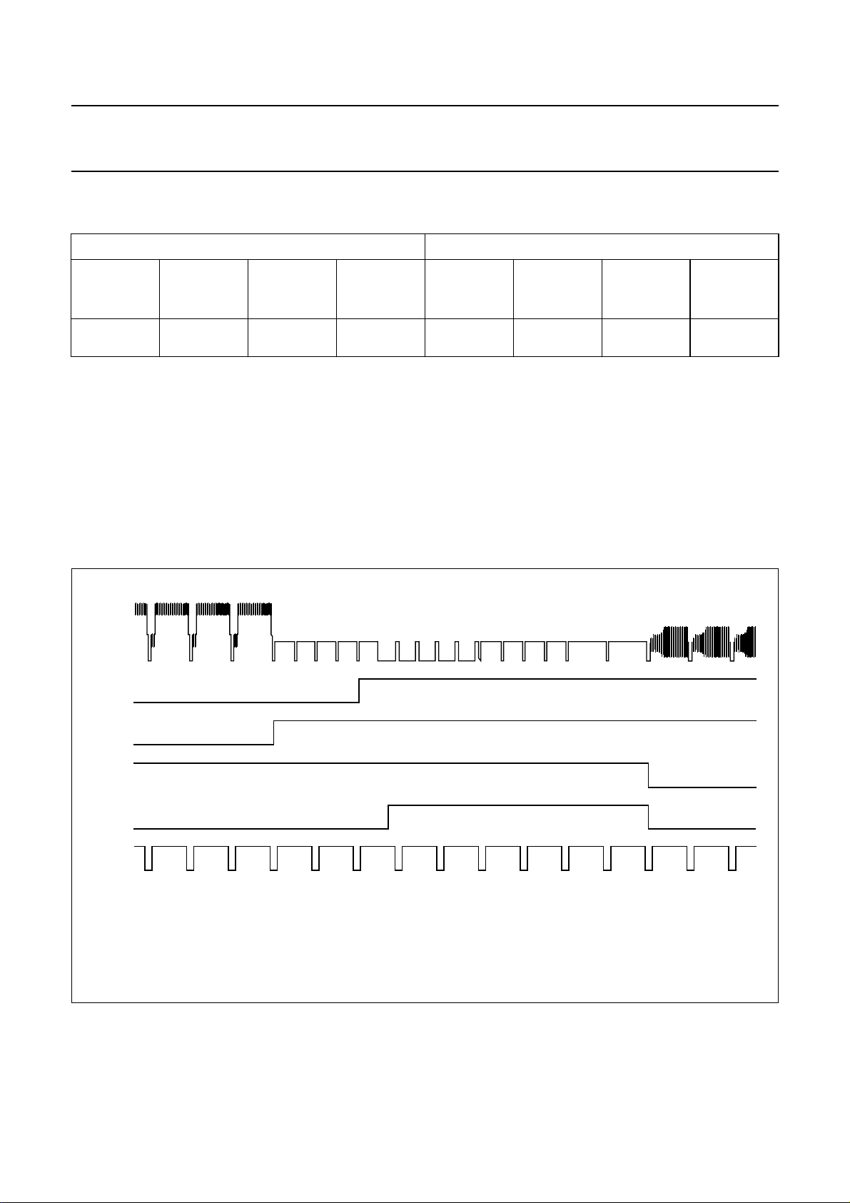
Philips Semiconductors Product specification
Multimedia bridge, high performance
SAA7146A
Scaler and PCI circuit (SPCI)
Table 54 Offsets to CCIR 656 line 23 depending on PAL or NTSC source (in compliance with Recommendation 601),
ODD and EVEN field and select mode (see note 1)
PAL NTSC
(4)
(2)
SLC
SAV/EAV
24 (25)
18H (19H)
SLC ext.
FS
15 (16)
0FH (10H)
(3)
SLC
FALLING
VS
15H (16)
0FH (10H)
(5)
SLC
RISING VS
21 (22)
15H (16H)
SLC
SAV/EAV
22 (22)
16H (16H)
SLC ext.
FS
12 (13))
0CH (0DH)
Notes
1. Line numbers in parenthesis refer to EVEN field counting.
2. Sync signal SLC with SAV/EAV detection (50H, SYNC_X = 7).
3. Sync signal SLC with external Field Identification Signal (50H, SYNC_X = 6).
4. Sync signal SLC with detection on the falling edge of the vertical sync signal (50H, SYNC_X = 1, 3 or 5).
5. Sync signal SLC with detection on the rising edge of the vertical sync signal. For Philips devices, the rising edge does
not include field information, this information is only defined at the falling edge of the VS signal (50H, SYNC_X = 0, 2
or 4).
SLC
FALLING
VS
12 (13)
0CH (0DH)
SLC
RISING VS
18 (19)
12H (13H)
7.8.8.1 Video with PAL format
handbook, full pagewidth
FID CCIR 656
VS CCIR 656
ODD SAA711x
VS SAA711x
LINES
(1) The line numbers not in parenthesis refer to CCIR counting.
(2) The line numbers in parenthesis refer to single field counting.
308
(308)
(1)
(2)
(309)
309
310
(310)
(311)
311
312
(312)
313
(313)
314
(1)
315
(2)
316
(3)
317
(4)
318
(5)
319
(6)
320
(7)
321
(8)
MHB057
Fig.15 Output timing of SAA711x, 50 Hz, lines 621 to 8.
1998 Apr 09 64
Page 65
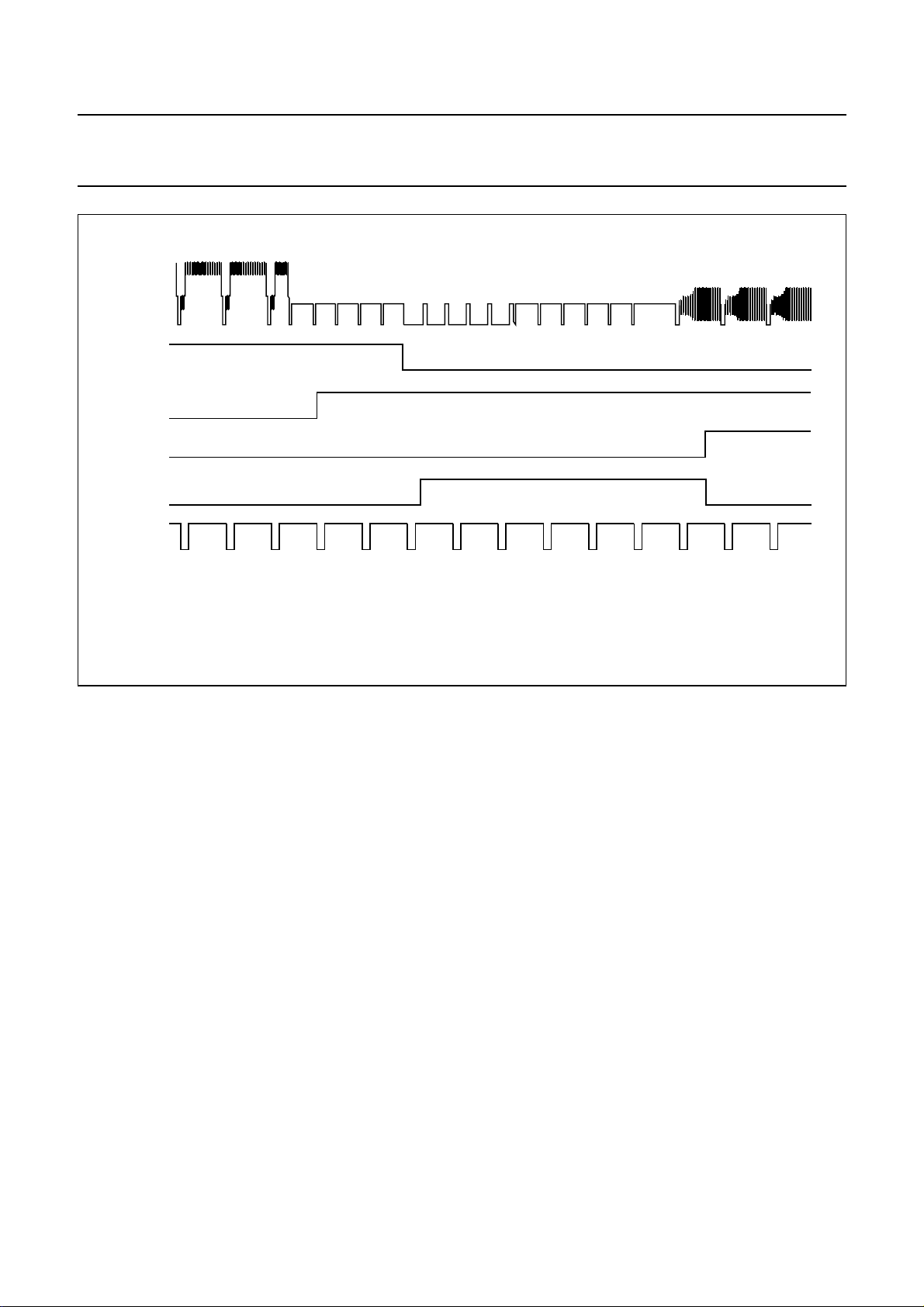
Philips Semiconductors Product specification
Multimedia bridge, high performance
Scaler and PCI circuit (SPCI)
handbook, full pagewidth
FID CCIR 656
VS CCIR 656
ODD SAA711x
VS SAA711x
LINES
621
(308)
(1)
(2)
(309)
622
623
(310)
(311)
624
625
(312)
(1)
SAA7146A
7
5
(6)
6
(7)
3
(4)
4
(5)
1
2
(3)
(2)
8
(8)
MHB056
(1) The line numbers not in parenthesis refer to CCIR counting.
(2) The line numbers in parenthesis refer to single field counting.
Fig.16 Output timing of SAA711x, 50 Hz, lines 308 to 321.
1998 Apr 09 65
Page 66
This text is here in white to force landscape pages to be rotated correctly when browsing through the pdf in the Acrobat reader.This text is here in
_white to force landscape pages to be rotated correctly when browsing through the pdf in the Acrobat reader.This text is here inThis text is here in
white to force landscape pages to be rotated correctly when browsing through the pdf in the Acrobat reader. white to force landscape pages to be ...
1998 Apr 09 66
Table 55 Comparison between CCIR 656 lines and the SLC (note 1)
(612)
(622)
CCIR 656
(D1) LINE
SLC
SAV/EAV
SLC ext.
(4)
FS
SLC falling
(5)
VS
SLC rising
(6)
VS
Notes
1. Line numbers in parenthesis refer to EVEN field counting.
2. CCIR 656 (D1) line.
3. SLC with SAV/EAV detection (50H, SYNC_X = 7).
4. SLC with external Field Identification Signal (50H, SYNC_X = 6).
5. SLC with detection on the falling edge of the vertical sync signal (50H, SYNC_X = 1, 3 or 5).
6. SLC with detection on the rising edge of the vertical sync signal. For Philips devices, the rising edge does not include field information, this
information is only defined at the falling edge of the VS signal (50H, SYNC_X = 0, 2 or 4).
(3)
(2)
310
311
(313)
302
(304)
302
(304)
308
(310)
(624)
311
312
(1)1(2)2(3)3(4)4(5)5(6)6(7)7(8)8(9)9(10)10(11)11(12)12(13)13(14)14(15)15(16)16(17)17(18)
303
(305)
(306)
303
(305)
(306)
309
(311)
(312)
(625)
312
3131(314)2(315)3(316)4(317)5(318)6(319)7(320)8(321)9(322)10(323)11(324)12(325)13(326)14(328)15(329)
304
305
306
307
308
304
310
(307)
305
(307)
311
(313)
309
(308)
(309)
(310)
(311)
306
307
308
309
(308)
(309)
(310)
(311)
312
(1)1(2)2(3)3(4)4(5)5(6)6(7)7(8)8(9)9(10)10(11)11(12)12(13)13(14)14(15)
310
(312)
310
(312)
311
(313)
311
(313)
312
(1)1(2)2(3)3(4)4(5)5(6)6(7)7(8)8(9)
312
(1)1(2)2(3)3(4)4(5)5(6)6(7)7(8)8(9)
Philips Semiconductors Product specification
Multimedia bridge, high performance
Scaler and PCI circuit (SPCI)
SAA7146A
Page 67
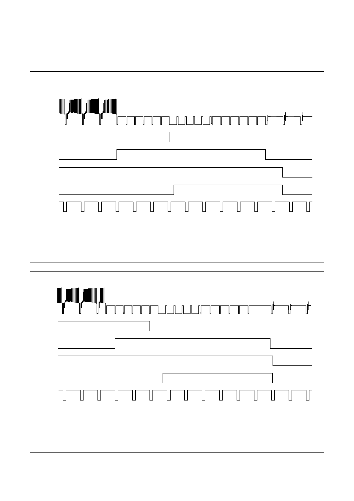
Philips Semiconductors Product specification
Multimedia bridge, high performance
Scaler and PCI circuit (SPCI)
7.8.8.2 Video with NTSC format
handbook, full pagewidth
FID CCIR 656
VS CCIR 656
ODD SAA711x
VS SAA711x
LINES
523
(260)
(1)
(2)
(261)
524
525
(262)
1
(1)
2
(2)
(3)
SAA7146A
10
6
(7)
7
(8)
4
3
(4)
(5)
5
(6)
9
8
(10)11(11)
(9)
MHB058
(1) The line numbers not in parenthesis refer to CCIR counting.
(2) The line numbers in parenthesis refer to single field counting.
Fig.17 Output timing of SAA711x, 60 Hz, lines 523 to 11.
handbook, full pagewidth
FID CCIR 656
VS CCIR 656
ODD SAA711x
VS SAA711x
LINES
261
(261)
(1)
(2)
(262)
262
263
(263)
264
(1)
265
(2)
266
(3)
267
(4)
268
(5)
269
(6)
270
(7)
271
(8)
272
(9)
273
(10)
274
(11)
MHB059
(1) The line numbers not in parenthesis refer to CCIR counting.
(2) The line numbers in parenthesis refer to single field counting.
Fig.18 Output timing of SAA711x, 60 Hz, lines 261 to 274.
1998 Apr 09 67
Page 68
This text is here in white to force landscape pages to be rotated correctly when browsing through the pdf in the Acrobat reader.This text is here in
_white to force landscape pages to be rotated correctly when browsing through the pdf in the Acrobat reader.This text is here inThis text is here in
white to force landscape pages to be rotated correctly when browsing through the pdf in the Acrobat reader. white to force landscape pages to be ...
1998 Apr 09 68
Table 56 Comparison between CCIR 656 lines and SLC (note 1)
CCIR 656
(D1) LINE
SLC
SAV/EAV
SLC ext.
(4)
FS
SLC falling
(5)
VS
SLC rising
(6)
VS
Notes
1. Line numbers in parenthesis refer to EVEN field counting.
2. CCIR 656 (D1) line.
3. SLC with SAV/EAV detection (50H, SYNC_X = 7).
4. SLC with external Field Identification Signal (50H, SYNC_X = 6).
5. SLC with detection on the falling edge of the vertical sync signal (50H, SYNC_X = 1, 3 or 5).
6. SLC with detection on the rising edge of the vertical sync signal. For Philips devices, the rising edge does not include field information, this
information is only defined at the falling edge of the VS signal (50H, SYNC_X = 0, 2 or 4).
(525)
(2)
2621(264)2(265)3(266)4(267)5(268)6(269)7(270)8(271)9(272)10(273)11(274)12(275)13(276)14(277)15(278)16(279)17(280)18(281)
262
(3)
(263)1(1)2(2)3(3)4(4)5(5)6(6)7(7)8(8)9(9)10(10)11(11)12(12)13(13)14(14)15(15)16(16)17(17)18(18)
252
(251)
252
(251)
258
(260)
253
(252)
253
(252)
259
(261)
254
(253)
254
(253)
260
(262)
255
(254)
255
(254)
261
(263)
256
257
258
259
260
261
262
(255)
(256)
(257)
(258)
(259)
256
257
258
259
(255)
(256)
(257)
(258)
(259)
262
(1)1(2)2(3)3(4)4(5)5(6)6(7)7(8)8(9)9(10)10(11)11(12)12(13)13(14)14(15)
260
(260)
(261)1(262)2(263)3(1)4(2)5(3)6(4)7(5)8(6)
261
262
(260)
(261)1(262)2(263)3(1)4(2)5(3)6(4)7(5)8(6)
Philips Semiconductors Product specification
Multimedia bridge, high performance
Scaler and PCI circuit (SPCI)
SAA7146A
Page 69

Philips Semiconductors Product specification
Multimedia bridge, high performance
Scaler and PCI circuit (SPCI)
7.9 High Performance Scaler (HPS)
Depending on the selected port modes the incoming and
scaled data are formatted/reformatted (8-bit or 16-bit), and
the corresponding reference signals are generated. Based
on these reference signals the active processing window is
defined in a versatile way via programming.
The programming register can be loaded during the
processing of the previous field, frame or line by RPS.
In this way each D1 port gets processed in a field or frame
alternating manner. If the incoming signals are not locked,
then the acquisition is waiting for the new active video of
the subsequent field. The corresponding fields are
detected by a ‘Field Detection’. To support asynchronous
video processing in the two video paths, each D1 port has
its own ‘Field Detection’. The video signal source is also
source for the qualify signal PXQ.
Before being processed in the central scaling unit the
incoming data passes to the BCS control unit, where
monitor control functions for adjusting Brightness and
Contrast (luminance) as well as Saturation (chrominance)
are implemented (BCS control). The horizontal scaling is
carried out in two steps; a prefiltering (bandwidth limitation
for initialising) and a horizontal fine scaling. Between them
the vertical processing is performed.
SAA7146A
7.9.2 S
The scaling to a randomly sized window is performed in
three steps:
• Horizontal prescaling (bandwidth limitation for
anti-aliasing, via FIR prefiltering and subsampling)
• Vertical scaling (generating phase interpolated or
vertically low-passed lines)
• Horizontal phase scaling (phase correct scaling to the
new geometric relations).
The scaling process generates a new pixel/clock qualifier
sequence. There are restrictions in the combination of
input sample rate and up or downscaling mode and scaling
factor. The maximum resulting output sample rate at the
DD1 port is
CCIR 656 format.
7.9.2.1 Horizontal prescaling
The incoming pixels in the selected range are
pre-processed in the horizontal prescaler (first stage of the
scaling unit). It consists of a FIR prefilter and a pixel
collecting subsampler.
7.9.2.2 FIR prefilter
CALING UNIT
1
⁄2LLC, because of compliance to the
7.9.1 BCS
The parameters for brightness, contrast and saturation
can be adjusted in the BCS control unit. The luminance
signal can be controlled by the bits BRIG7 to BRIG0 and
CONT6 to CONT0. The chrominance signal can be
controlled by the bits SAT6 to SAT0.
Brightness control (BRIG7 to BRIG0):
• 00H; minimum offset
• 80H; CCIR level
• FFH; maximum offset.
Contrast control (CONT6 to CONT0):
• 00H; luminance off
• 40H; CCIR level
• 7FH; 1.9999 amplitude.
Saturation control (SAT6 to SAT0):
• 00H; colour off
• 40H; CCIR level
• 7FH; 1.9999 amplitude.
Limits: All resulting output values are limited to minimum
(equals 0) and maximum (equals 255).
CONTROL
The video components Y, U and V are FIR pre-filtered to
reduce the signal bandwidth according to the downscale
for factors between 1 and1⁄2, so that aliasing, due to signal
bandwidth expansion, is reduced. The prefilter consists of
3 filter stages. The transfer functions are listed in the
Section 7.12. The prefilter is controlled by the ‘Scaler
Register’ bits PFY3 to PFY0 and PFUV3 to PFUV0 in the
HPS horizontal prescale register (see Table 79).
Figures 19 and 20 show frequency response
characteristics and the corresponding scaler register
settings. The prefilter operates on YUV 4:4:4 data.
As U and V are generated by simple chroma pixel
doubling, the UV prefilter should also be used to generate
the interpolated chroma values.
7.9.2.3 Subsampler
To improve the scaling performance for scales less than
1
⁄2down to icon size, a FIR filtering subsampler is
available. It performs a subsampling of the incoming data
by a factor of 1/N, where N = 1 to 64. This operation is
controlled by XPSC, where N = XPSC + 1. Where
NIP = number of input pixels/line and NOP = number of
desired output pixels/line, the basic equation to calculate
XPSC is:
XPSC = TRUNC [(NIP/NOP) − 1]
1998 Apr 09 69
Page 70
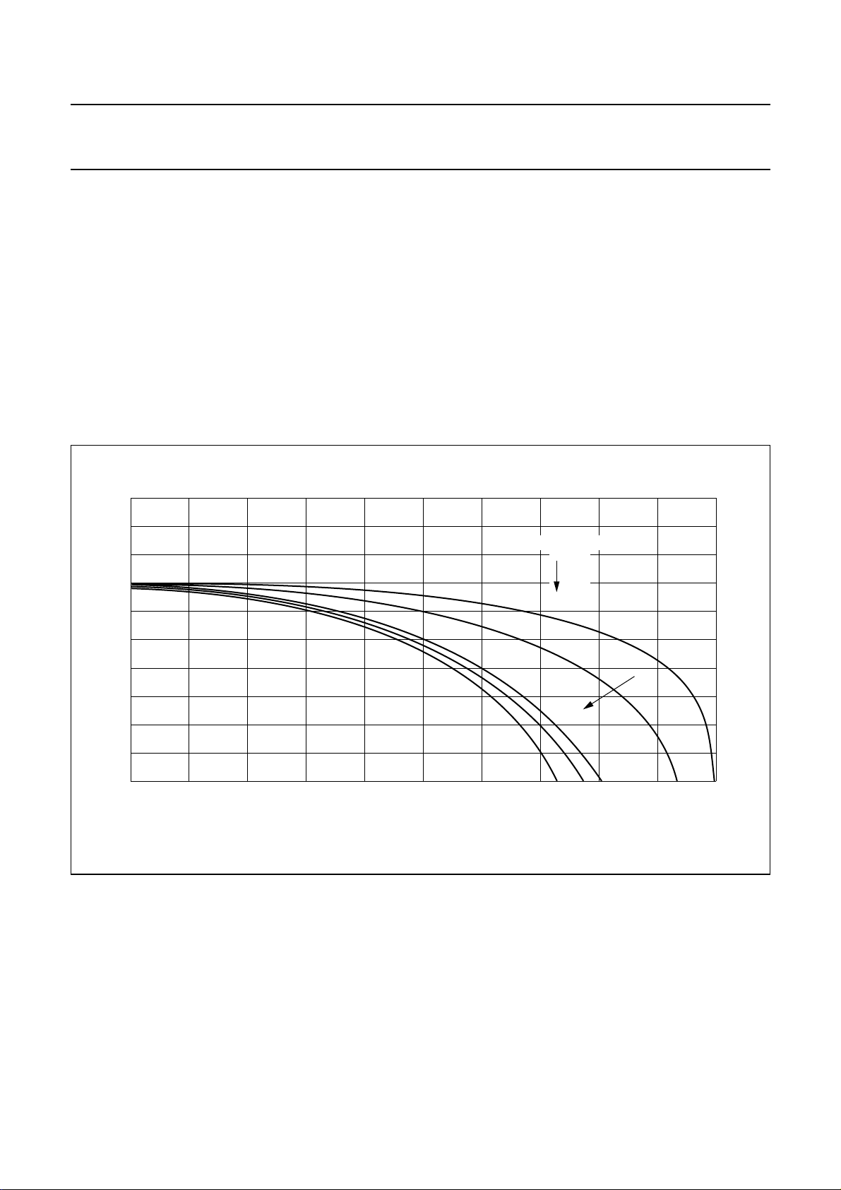
Philips Semiconductors Product specification
Multimedia bridge, high performance
Scaler and PCI circuit (SPCI)
The subsampler collects a number of [XPSC + 2 − XACM]
pixels to calculate a new subsampled output pixel. So a
downscale dependent FIR filter is built with up to 65 taps
which reduces anti-aliasing for small sizes. If XACM = 0,
the collecting sequence overlaps which means that the
last pixel of sequence M is also the first pixel of sequence
M+1.
To implement a real subsampler bypass, XACM has to be
set to logic 1.
As the phase correct horizontal fine scaling is limited to a
maximum downscale of1⁄4, this circuitry has to be used for
downscales less than1⁄4 of the incoming pixel count.
18
handbook, full pagewidth
12
dB
6
0
−6
SAA7146A
To get unity gain at the subsamplers output for all
subsampling ratios, the scaler register parameters CXY,
CXUV and DCGX have to be used. In addition, this can be
used to modify the FIR characteristic of the subsampler
slightly. Table 57 illustrates examples for scaler register
settings, depending on a given prescale ratio. Referring to
Table 57(divider in column ‘Weight Sum’) it should be
noted that an internal XPSC depending automatic
prenormalization is valid for:
XPSC > 8, > 16, > 32, which reduces the input signal
quantization. In addition it should be noted that for
XPSC ≥ 15 the LSB of the CXY,CXUV parameter
becomes valid.
MGG263
PFY3 to PFY0
0001
0010
0011
1011
1111
−12
−18
−24
−30
−36
−42
0 0.5
0.1 0.2 0.3 0.4
MHz
Fig.19 Luminance Prefilter: frequency response for miscellaneous register settings.
1998 Apr 09 70
Page 71
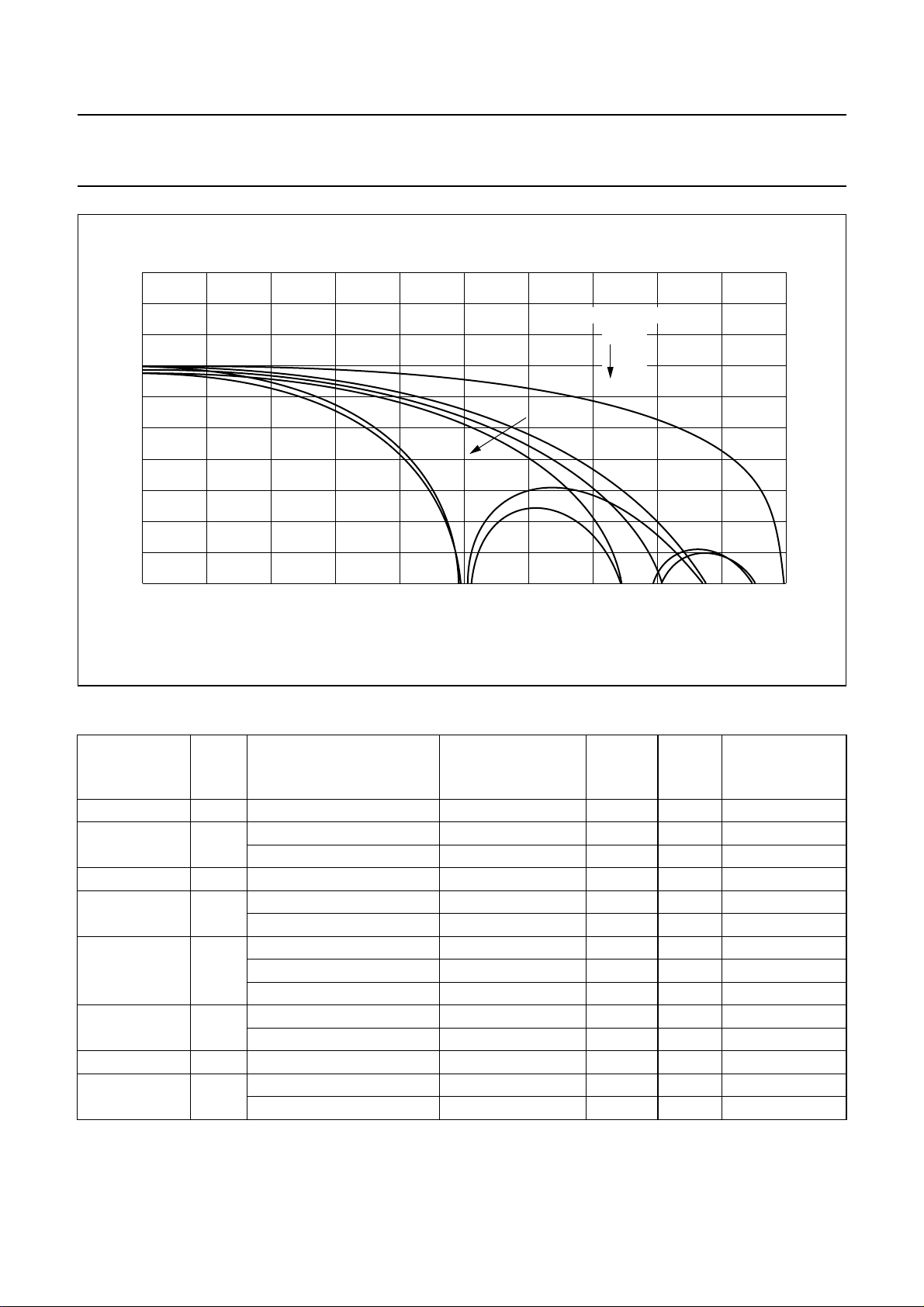
Philips Semiconductors Product specification
Multimedia bridge, high performance
Scaler and PCI circuit (SPCI)
18
handbook, full pagewidth
12
dB
6
0
−6
−12
−18
−24
−30
−36
−42
0 0.5
0.1 0.2 0.3 0.4
PFUV3 to PFUV0
0001
0010
0011
1111
1010
1110
SAA7146A
MGG264
MHz
Fig.20 Chrominance Prefilter: frequency response for miscellaneous register settings.
Table 57 Horizontal prescaling and normalization
HORIZONTAL
PRESCALER
XPSC
COEFFICIENT
SEQUENCE (EXAMPLE)
1 0 1-1 0 0 2 1 1
1
⁄
2
1 1-1-1 0 0 3 1
1-2-1 0 2 4 2 1
1
⁄
3
1
⁄
4
2 1-1-1-1 0 0 4 2 1
3 1-1-1-1-1 0 0 5 2
1-2-2-2-1 0 6 8 3 1
1
⁄
5
4 111 111 0 0 6 2
121 121 0 2 8 3 1
112 211 0 4 8 3 1
1
⁄
6
5 1111111 00 7 3
1112111 08 8 3 1
1
⁄
7
1
⁄
8
6 1111 1111 0 0 8 3 1
7 1111 1 1111 0 0 9 3
1222 2 2221 1 E 16 7 1
CXY (LUMINANCE)
CXUV (CHROMA)
WEIGHT
SUM
DCGX
BCS
(CONTR. | SAT.)
= X/Y × 64
2
⁄
3
4
⁄
5
4
⁄
6
8
⁄
7
8
⁄
9
1998 Apr 09 71
Page 72
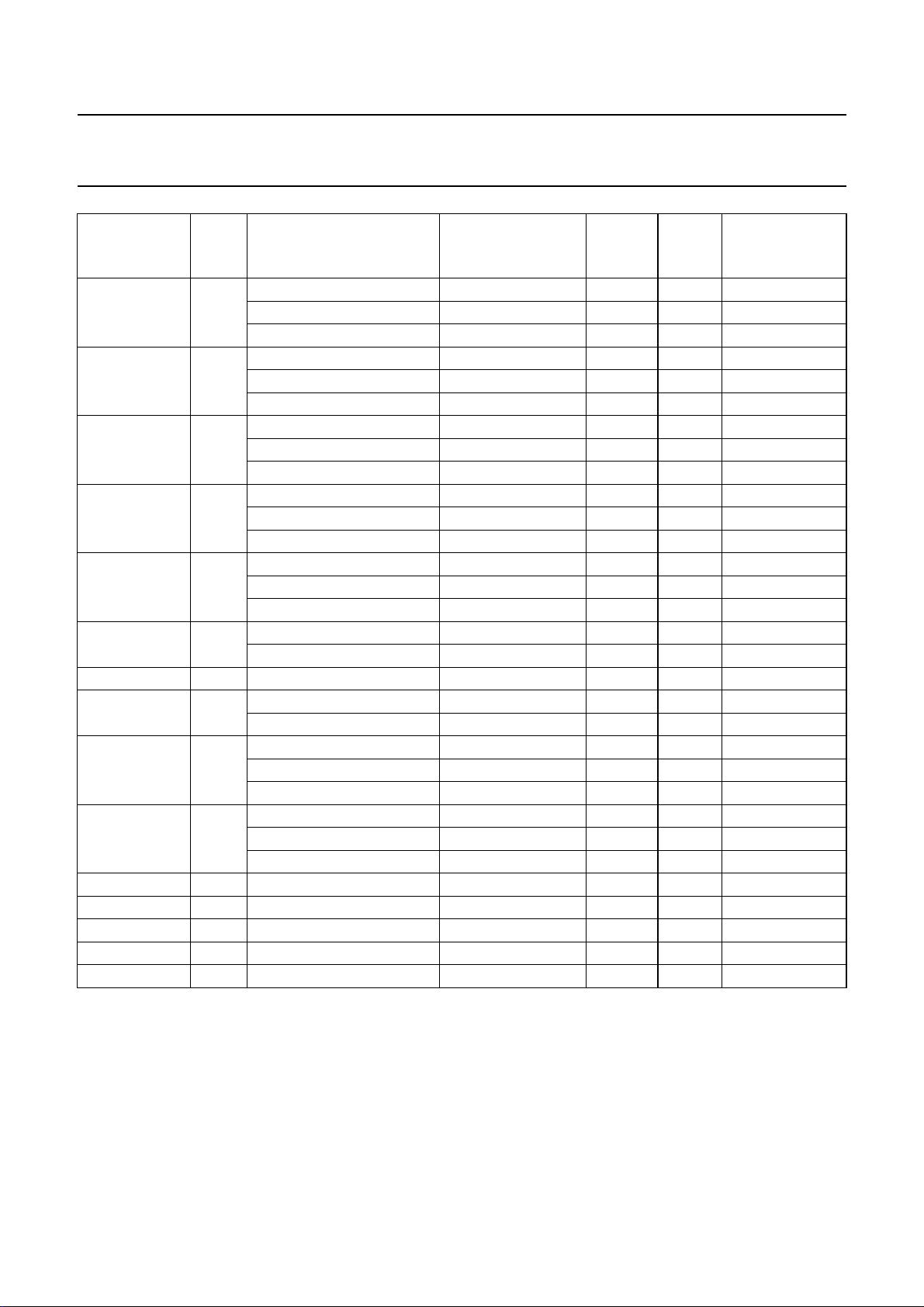
Philips Semiconductors Product specification
Multimedia bridge, high performance
SAA7146A
Scaler and PCI circuit (SPCI)
HORIZONTAL
PRESCALER
1
⁄
9
XPSC
8 1111111111 00 10/2 2
COEFFICIENT
SEQUENCE (EXAMPLE)
CXY (LUMINANCE)
CXUV (CHROMA)
WEIGHT
SUM
DCGX
1221 2 2 1221 1 6 16/2 31
1122 2 2 2211 1 C 16/2 31
1
⁄109 1111 1 1 1 1111 0 0 11/2 2
1212 1 2 1 2121 2 A 16/2 31
11122222111 38 16/2 31
1
⁄1110 1111 11 11 1111 0 0 12/2 2
1211 21 12 1121 1 2 16/2 31
1111 22 22 1111 3 0 16/2 31
1
⁄1210 1111 11 1 11 1111 0 0 13/2 2
1121 11 2 111211 4 4 16/2 31
1111122211111 60 16/2 31
1
⁄1310 1111 111 111 1111 0 0 14/2 2
1111 211112 1111 1 0 16/2 31
1111 112 211 1111 4 0 16/2 31
1
⁄1410 1111 111 1 111 1111 0 0 15/2 2
1111 111 2 111 1111 8 0 16/2 31
1
⁄1514 1111 1111 1111 1111 0 0 16/2 31
1
⁄1615 1111 1111 1 1111 1111 − 17/2 3
1222 2222 2 2222 2221 F F 32/2 71
1
⁄1716 1111 1111 1 1 1111 1111 0 0 18/4 2
1222 2222 1 1 2222 2221 F E 32/4 31
1222 2122 22 2212 2221 D F 32/4 31
1
⁄1817 1111 1111 1 1 1 1111 1111 0 0 19/4 2
1222 1222 1 2 1 2221 2221 E E 32/4 31
1222 211222221122221 9 F 32/4 31
−− − − xx/4 −−
1
⁄3332 1111...1111 0 0 34/8 2 −
−− − − xx/8 −−
1
⁄6362 −−−−−
1
⁄
64
63 −−−−−
BCS
(CONTR. | SAT.)
= X/Y × 64
8
⁄
10
8
⁄
11
8
⁄
12
8
⁄
13
8
⁄
14
8
⁄
15
16
⁄
17
16
⁄
18
16
⁄
19
1998 Apr 09 72
Page 73

Philips Semiconductors Product specification
Multimedia bridge, high performance
Scaler and PCI circuit (SPCI)
7.9.2.4 Vertical scaler
The vertical scaler performs the vertical downscaling of the
input data stream to a randomly number of output lines.
It can be used for input line lengths up to 768 pixels/line
and has to be bypassed, if the input line length exceeds
this pixel count.
For the vertical scaling there are two different modes:
• The ACCU mode (vertical accumulation) for scales
down to icon size and
• The Linear Phase Interpolation (LPI) mode for scales
between 1 and
7.9.2.5 ACCU mode (scaling factor range 1 to 1/1024;
For vertical scales down to icon size the ACCU mode can
be used. In this mode the parameter YSCI controls the
scaling and the parameter YACL the vertical anti-aliasing
filtering.
The output lines are generated by a scale-dependent
variable averaging of (YACL + 2) input lines. In this way a
vertical FIR filter is build for anti-aliasing, with up to
maximum 65 taps.
YSCI defines the output line qualifier pattern and YACL
defines the sequence length for the line averaging.
For accurate processing the sequence has to fit into the
qualifying pattern. In case of misprogramming YACL,
unexpected line dropping occurs.
Where:
• NOL= Number of Output Lines and
• NIL= Number of Input Lines.
1
⁄2.
YACM = 1)
SAA7146A
the YSCI (scaling increment), YACL (accumulation length;
optimum: 1 line overlap) and YP (scaling start phase) have
to be set according to the equations below, see Fig.21.
• YACL = TRUNC [N
length; i.e. number of lines per sequence, that are not
part of overlay region of neighbouring sequences
(optimum: 1 line overlapped)
• YSCI = INT [1024 × (1 − NOL/NIL)] scaling increment
• YPx = INT [YSCI/16] scaling start phase (fix; modified in
LPI mode only).
In order to get a unity amplitude gain for all sequence
lengths and to improve the vertical scaling performance,
the accumulated lines can be weighted and the amplitude
of the scaled output signal has to be renormalized. In the
given example (see Fig.21), using the optimal weighting,
the gain of a sequence results in 1 + 2 + 2 + 1 = 6.
Renormalization (factor1⁄6) can be done
• By gain reduction using BCS control (brightness,
contrast, saturation) down to4⁄6 and selecting factor1⁄
for DCGY2 to DCGY0 which may result in a loss of
signal quantization, or
• By gain emphasizing using BCS control up to8⁄
and selecting factor1⁄8 for DCGY2 to DCGY0 which
may result in a loss of signal detail due to limiting in the
BCS control.
Normally, the weighting would be 2 + 2 + 2 + 2. In this
case the gain can be renormalized simply with
DCGY2 to DCGY0 = ‘010’ (factor1⁄8). Table 58 gives
examples for register settings depending on a given scale
ratio.
− 1] accumulation sequence
IL/NOL
6
4
handbook, full pagewidth
line 1 1
line 2
scaling factor S = 1/3: vertical accumulation of 4 lines (1 line overlap)
optimal weighting factors:
1st sequence
2nd sequence
3rd sequence
2
2
1
2
2
1
2
2
1
Fig.21 Example: vertical accumulation.
1998 Apr 09 73
YACL = INT {(1 - S)/S}
YSCI = INT {1024 × (1 - S)}
YP x = INT {YSCI/16}
= 2 (dotted lines)
= 682
= 42
MGD697
Page 74
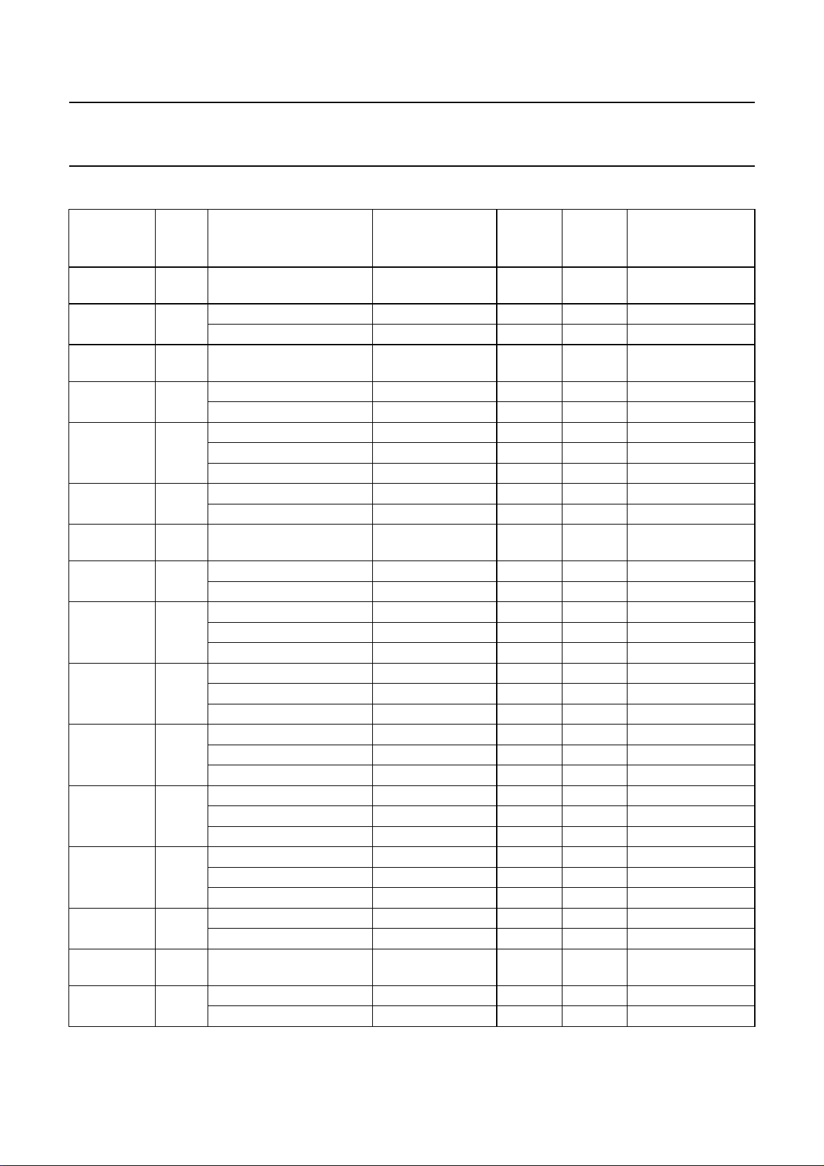
Philips Semiconductors Product specification
Multimedia bridge, high performance
Scaler and PCI circuit (SPCI)
Table 58 Vertical scaling and normalization
VERTICAL
SCALE
RATIO
1
⁄
1to
2
(0)
1
⁄2to1⁄
3
(512)
1
⁄3to1⁄
4
(683)
1
⁄4to1⁄
5
(768)
1
⁄5to1⁄
6
(820)
1
⁄6to1⁄
7
(854)
1
⁄7to1⁄
8
(878)
1
⁄8to1⁄
9
(896)
1
⁄9to1⁄
10
(911)
1
⁄10to1⁄
11
(922)
1
⁄11to1⁄
12
(931)
1
⁄12to1⁄
13
(939)
1
⁄13to1⁄
14
(946)
1
⁄14to1⁄
15
(951)
1
⁄15to1⁄
16
(956)
1
⁄16to1⁄
17
(960)
YACL
0 1-1 01, 00 2 0 1
1 1-1-1 03, 00 3 0
2 1-1-1-1 03, 00 4 1 1
3 1-1-1-1-1 07, 00 5 1
4 111 111 07, 00 6 1
5 1111111 0F,00 7 2
6 1111 1111 0F, 00 8 2 1
7 111111111 1F,00 9 2
8 1111 1 1 1111 1F, 00 10 3
9 11111111111 3F,00 11 2
10 1111 11 11 1111 3F, 00 12 2
11 1111111111111 7F,00 13 2
12 1111 111 111 1111 7F, 00 14 2
13 1111 111 1 111 1111 FF, 00 15 2
14 1111 1111 1111 1111 FF, 00 16 3 1
15 1111 1111 1 1111 1111 FF, 00 17 3
COEFFICIENT
SEQUENCE (EXAMPLE)
1-2-1 01, 02 4 1 1
1-2-2-2-1 01, 06 8 2 1
121 121 05, 02 8 2 1
112 211 03, 04 8 2 1
111 2 111 07, 08 8 2 1
1222 2 2221 01, 1E 16 3 1
2121 2 2 1212 09, 15 16 3 1
1122 2 2 2211 03, 1C 16 3 1
1212 1 2 1 2121 15, 2A 16 3 1
11122222111 07,38 16 3 1
1211 21 12 1121 2D, 12 16 3 1
1111 22 22 1111 0F, 30 16 3 1
1111212121111 2F,50 16 3 1
1121 11 2 111211 3B, 44 16 3 1
1111 211112 1111 6F, 10 16 3 1
1111 112 211 1111 3F, 40 16 3 1
1111 111 2 111 1111 7F, 80 16 3 1
2122 2222 2 2222 2212 02, FD 32 4 1
CYA; CYB
WEIGHT
SUM
DCGY
SAA7146A
BCS
(CONTR. | SAT.)
= X/Y × 64
2
⁄
3
4
⁄
5
4
⁄
6
8
⁄
7
8
⁄
9
8
⁄
10
8
⁄
11
8
⁄
12
8
⁄
13
8
⁄
14
8
⁄
15
16
⁄
17
1998 Apr 09 74
Page 75
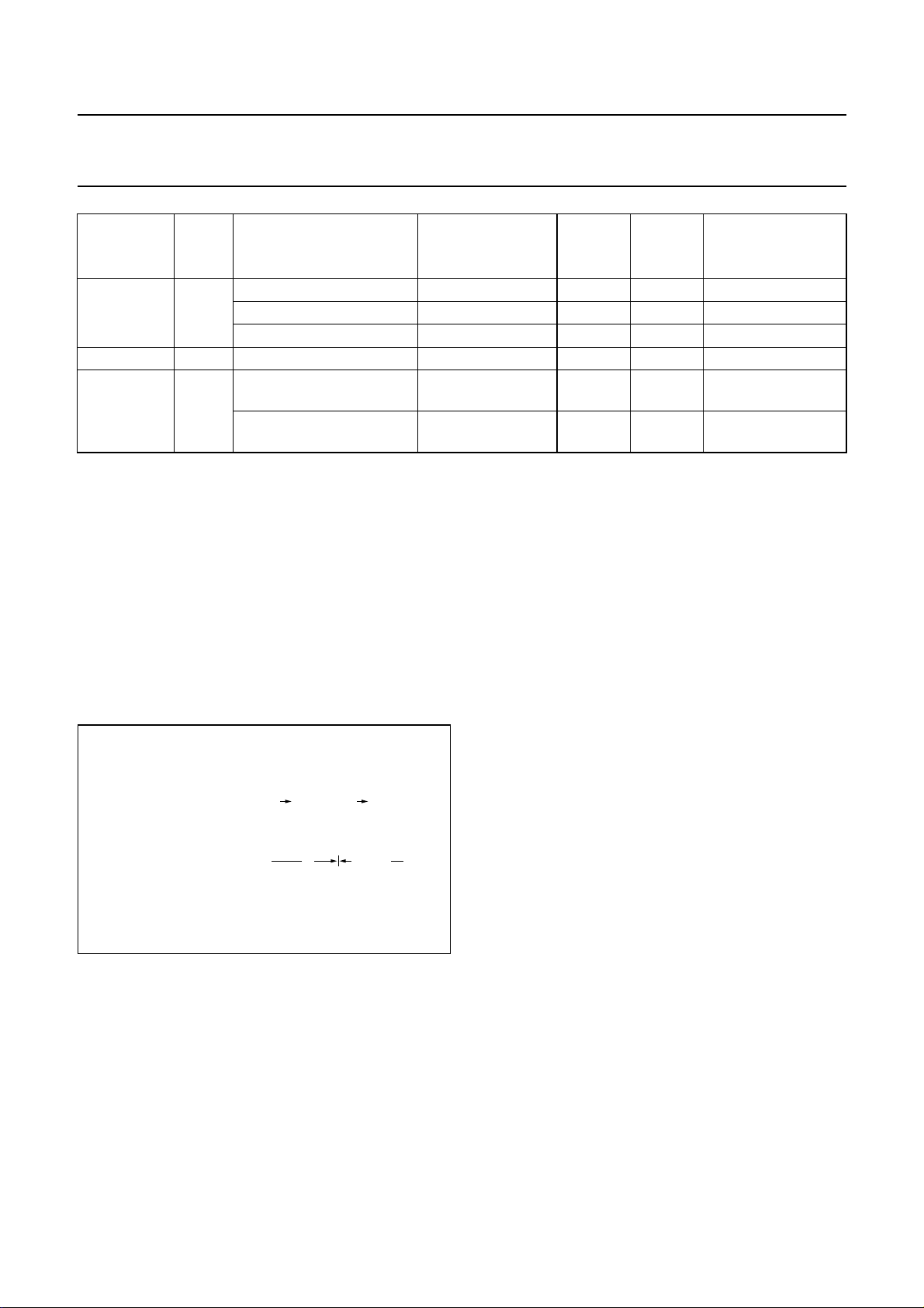
Philips Semiconductors Product specification
Multimedia bridge, high performance
Scaler and PCI circuit (SPCI)
VERTICAL
SCALE
YACL
RATIO
1
⁄17to1⁄
18
16 1111 1111 1 1 1111 1111 FF, 00 18 3
(964)
... ... ... ... ... ... ...
1
⁄23to1⁄
24
22 1111 2222 1111
(980)
7.9.2.6 LPI mode (scaling factor range 1 to
bit YACM = 0)
To preserve the signal quality for slight vertical
downscales (scaling factors 1 to1⁄2) Linear Phase
Interpolation (LPI) between consecutive lines is
implemented to generate geometrically correct vertical
output lines. Thus, the new geometric position between
lines N and N + 1 can be calculated.
A new output line is calculated by weighting the samples
‘p’ of lines N and N + 1 with the normalized distance to the
newly calculated position:
handbook, halfpage
new calculated position line
of output line M
input lines
Fig.22 Calculation of output lines.
p(M) = A × p(N + 1) + (1 − A) × p(N); where A = 0 to
With NOL= Number of Output Lines and NIL= Number of
Input Lines the scaler register bits YSCI (scaling
increment) and YP (scaling start phase) have to be set
according to the following equations:
• YSCI = INT [1024 × (NIL/(NOL− 1)] scaling increment
• YPx = INT [
YSCI
⁄16] scaling start phase (recommended
value).
COEFFICIENT
SEQUENCE (EXAMPLE)
CYA; CYB
WEIGHT
SUM
DCGY
2212 2212 2 2 2122 2122 44, BB 32 4 1
1222 2222 1 1 2222 2221 01, FE 32 4 1
0F, F0 32 4 1
1111 2222 1111
1121 1212 1121
AD, 52 32 4 1
1211 2121 1211
1
⁄
; register
2
The vertical start phase offset is defined by
YP
⁄64(YP=0to64):
• YP = 0: offset = 0 geometrical position of 1st
line
= 1st line
out
in
• YP = 64: offset =64⁄64= 1 geometrical position of
1st line
= 2nd linein.
out
Finally 3 special modes are to be emphasized:
1. Bypass (YSCI = 0, YP = 64); each line
to corresponding line
in
2. Low-pass (YSCI = 0, YP < 64); e.g. YP = 32: average
value of 2 lines (1 + z−h filter)
3. For processing of interlaced input signals the LPI
mode must be used (ACCU mode would cause ‘line
pairing’ problems). The scaling start phase for odd and
even field have to be set to:
N Distance = 1 N + 1
I I
I M I
A (1 − A)
MHB107
YP
In modes 1 and 2 the first input line is fed to the output
(without processing), so that the number of output lines
equals the number of input lines
even
=3⁄2× YP
(line 1 = odd)
odd
7.9.2.7 Flip option (Mirror = 1)
For both vertical scaling modes there is a flip option
‘mirroring’ available for input lines with a maximum of
384 pixels. In the case of full screen pictures (e.g.
63
768 × 576) that have to be flipped, they first have to be
⁄64.
downscaled to 384 pixel/line in the horizontal prescaling
unit and after vertical processing (flipping) they may be
rezoomed to the original 768 pixels/line in the following
VPD.
It should be noted that, when using the flip option, the last
input line can not be displayed at the output.
SAA7146A
BCS
(CONTR. | SAT.)
= X/Y × 64
16
⁄
18
is equivalent
out
1998 Apr 09 75
Page 76

Philips Semiconductors Product specification
Multimedia bridge, high performance
Scaler and PCI circuit (SPCI)
7.9.3 HORIZONTAL PHASE SCALING
In the phase correct Horizontal Phase Scaling (HPS) the
pixels are calculated for the geometrically correct,
orthogonal output pattern, down to1⁄4of the prescaled
pattern. A horizontal zooming feature is also supported.
The maximum zooming factor is at least 2, even more
dependent on input pattern and prescaling settings.
The phase scaling consists of a filter and an arithmetic
structure which is able to generate a phase correct new
pixel value almost without phase or amplitude artefacts.
The required sample phase information is generated by a
sample phase calculator, with an accuracy of
pixel distance. The up/downscaling with this circuitry is
controlled by the scaler register parameters XSCI and XP.
As the fine scaling is restricted to downscales >(1⁄4 of the
fine scalers input pixel count), XSCI is also a function of
the prescaling parameter XPSC.
With NIP= Number of Input Pixel/line (at DD1 input) and
NOP= Number of desired Output Pixels/line, XSCI is
defined to:
XSCI = INT [(NIP/NOP) × 1024/(XPSC + 1)]
The maximum value of XSCI = 4095. Zooming is
performed for XSCI values less than 1024. The number of
disqualified clock cycles between consecutive pixel
qualifiers (at the fine scalers input) defines the maximum
possible zoom factor. Consequently, zooming may also be
a function of XPSC. It should be noted that if the zooming
factor is greater than 2, some artefacts may occur at the
end of the zoomed line.
7.9.4 C
The scaled YUV output data is converted after
interpolation into RGB data according to CCIR 601
recommendations. The CSM is bypassed in all YUV
formats or monochrome modes.
The matrix equations considering the digital quantization
are:
R = Y + 1.375V
G=Y−0.703125V − 0.34375U
B = Y + 1.734375U.
OLOUR SPACE MATRIX (CSM), DITHER AND
γ-CORRECTION
1
⁄64 of the
SAA7146A
The ‘Chroma Signal Key’ generates an alpha signal used
in several RGB formats. Therefore, the processed UV data
amplitudes are compared with thresholds. A logic 1 is
generated, if the amplitude is within the specified
amplitude range. Otherwise a logic 0 is generated. Keying
can be switched off by setting the lower limit higher than
the upper limit!
7.10 Binary Ratio Scaler (BRS)
7.10.1 G
The BRS is the second scaler in the SAA7146A. The BRS
is supposed to support different encoder applications while
the HPS is processing video data. The BRS does not
support clipping.
The mainstream application of the BRS is to read data via
PCI, e.g. a QCIF-formatted video data to proceed with
horizontal and vertical upscaling to CIF-format and place it
at the encoder’s disposal (normal playback mode).
To support CCIR encoder and square pixel encoder, an
active video window as input for the BRS can be defined.
It will prevent black pixels being displayed at the end of the
line or at the bottom of the field.
The BRS supports only the YUV 4:2:2 video data format
(see Section 7.11.2). The used DD1 I/O data format is
8-bit. The BRS uses video DMA Channel 3 (FIFO 3) which
is only available, if the HPS is not in planar mode or writes
back clip information.
Vertical upscaling is supported by means of repeated
reading of the same line via PCI. Vertical downscaling is
achieved by line dropping.
Horizontal downscaling is performed by an accumulating
FIR filter. The downscaling is available for the inbound
mode and the upscaling is available for the outbound
mode (see Figs 23 and 24).
• Vertical ratios: 4, 2, 1,1⁄2and1⁄4; select with BRS_V
• Horizontal ratios: 8, 4, 2, 1,1⁄2,1⁄4 and1⁄8; select with
BRS_H.
If the data is sent from DD1 to PCI, the processing window
for the BRS scaling unit is defined in the acquisition control
(see Section 7.8.7).
ENERAL DESCRIPTION
A dither algorithm is implemented for error diffusion. ROM
tables are implemented at the matrix output to provide
anti-gamma correction of the RGB data. A curve for a
gamma of 1.4 is implemented. The tables can be used to
compensate gamma correction for linear data
representation of RGB output data.
1998 Apr 09 76
Page 77
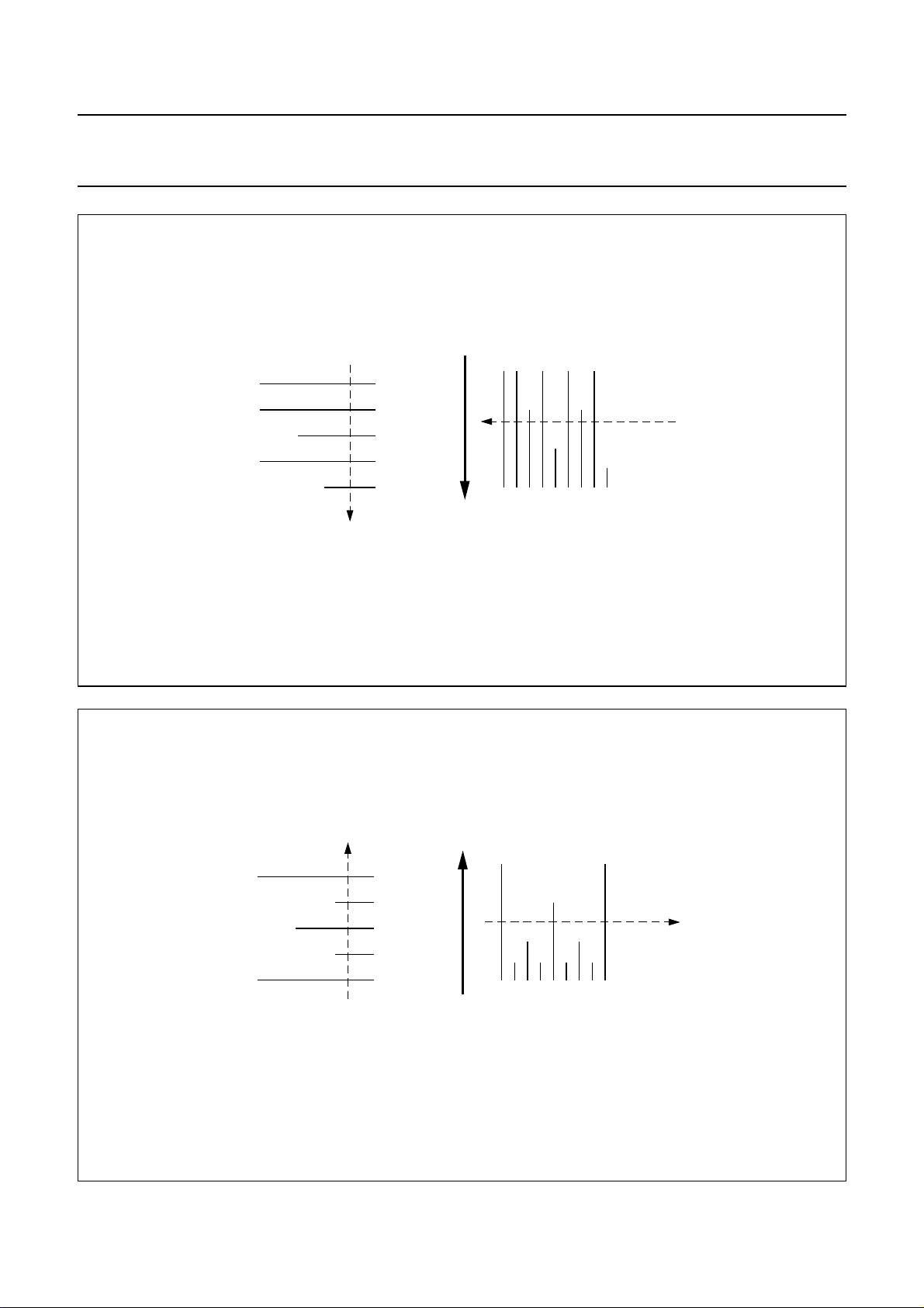
Philips Semiconductors Product specification
Multimedia bridge, high performance
Scaler and PCI circuit (SPCI)
handbook, full pagewidth
1
vertical
1/2
1/4
line dropping
downscaling
D1
PCI
(DMA3)
1
1/2
1/4
accumulating FIR
SAA7146A
horizontal
1/8
MHB060
handbook, full pagewidth
2
1
line repetition
vertical
4
Fig.23 BRS inbound mode.
D1
upscaling
PCI
(DMA3)
4
8
linear interpolation
1
2
horizontal
MHB061
Fig.24 BRS outbound mode.
1998 Apr 09 77
Page 78
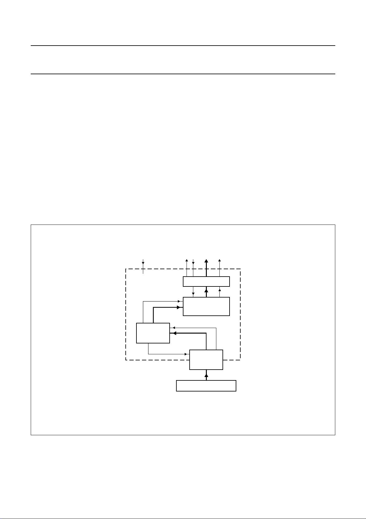
Philips Semiconductors Product specification
Multimedia bridge, high performance
Scaler and PCI circuit (SPCI)
The PCI source data is defined by the base address
(BaseOdd3 and BaseEven3), the distance between the
start addresses of two consecutive lines of a field (Pitch3),
the number of lines per field of the source frame
(NumLines3) and the number of bytes per line of the
source frame (NumByte3). The programmer must provide
correct scaling settings to fulfil the target window
requirements. The pitch has to be Dword aligned.
7.10.2 P
The SAA7146A offers three different modes to support the
playback mode for various systems. The Binary Ratio
Scaler (BRS) inputs data from FIFO 3, therefore the DMA3
is in master read operation. The scaling result is passed to
the DD1 output.
The following sections describe the three different modes:
field memory mode, direct mode and line memory mode.
LAYBACK MODE
SAA7146A
7.10.2.1 Field memory mode
In the field memory mode the SAA7146A takes a vertical
sync signal as a timing reference signal. A reset signal for
a field memory and a PXQ as write enable are generated
within the circuit and both are sent to port A or port B.
In this mode the pixel clock depends on the PCI load.
The pixels are provided to the DD1 port with maximum
1
⁄2LLC (CCIR 656), the picture rate is restricted by the
vertical timing reference. Since the transfer works without
losing any data the pixel clock can be varied, therefore an
external field memory is needed at the DD1 interface.
The SAA7146A writes its data continuously to this
memory. The video window size depends on the selected
window size in the system memory, the frame buffer
(Numlines, Numbytes, pitch and base address) and the
selected scaling ratio.
handbook, full pagewidth
LLC
PXQ
DMA
READ
field
reset
DATA
Dword request
DATAVS
D1 INTERFACE
FIFO empty
DATA
FIFO3
PXQ
(write enable)
BRS
PCI
MGG266
Fig.25 Sync and data path for field memory mode.
1998 Apr 09 78
Page 79
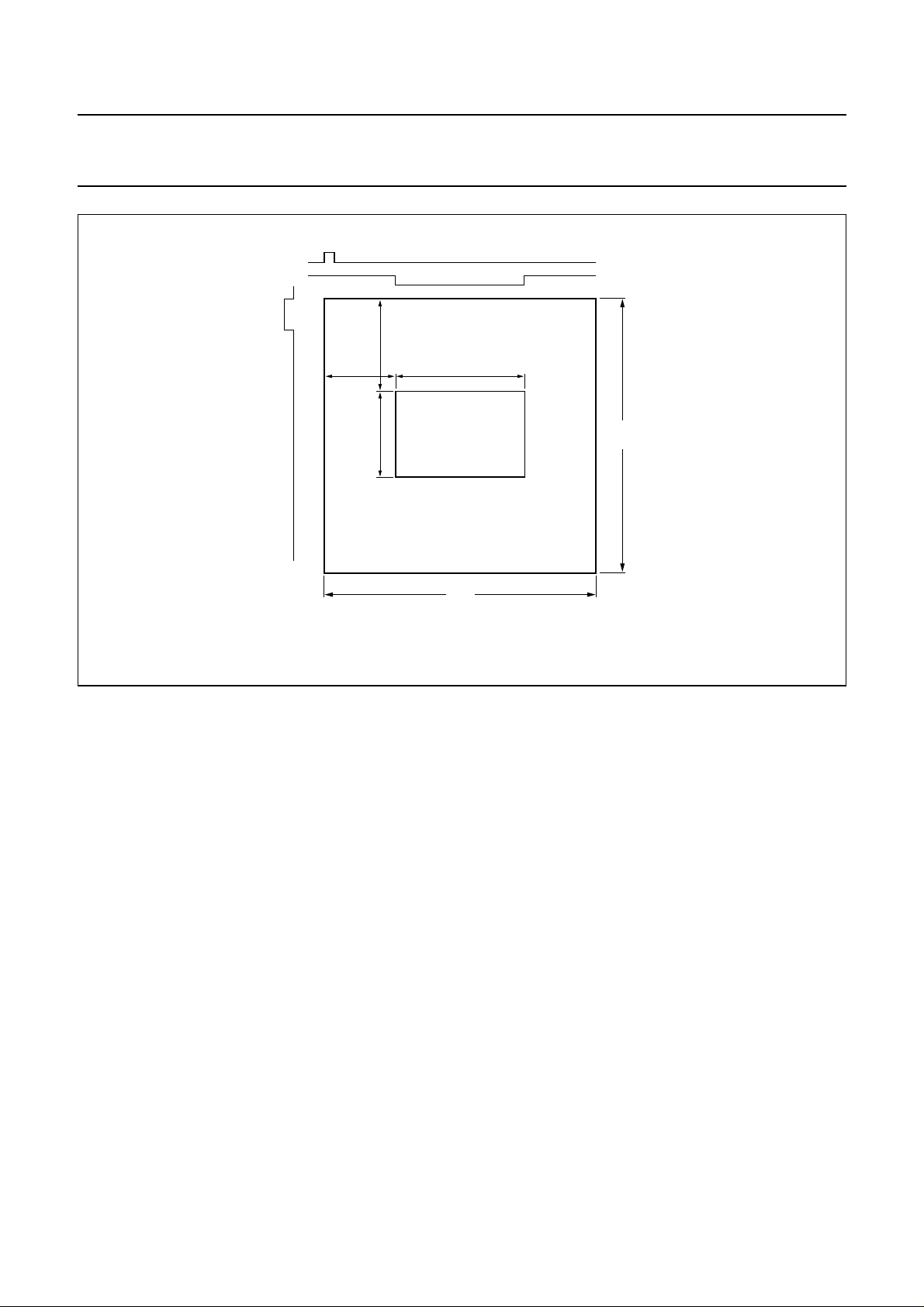
Philips Semiconductors Product specification
Multimedia bridge, high performance
Scaler and PCI circuit (SPCI)
handbook, full pagewidth
VS
ACTIVE VIDEO WINDOW
BYO
BXO
(NumBytes/2) × scale ratio
NumLines × scale ratio
SCALING
result
WINDOW
line
SAA7146A
HS
PXQ (only in direct mode)
field/
frame
MGG265
Fig.26 Reference signals for scaling window for direct and line memory mode.
7.10.2.2 Direct mode
The timing reference signals (VS, HS, LLC and FID) are
taken from port A or port B. The BRS has to deliver pixel
with pixel clock of1⁄2LLC to the D1 port. To ensure that
there are no dropouts, a simple underflow handling is
performed by the DMA read module. If the PCI load is big
and a FIFO underflow occurs, the DMA read module uses
a grey value (10H for luminance, 80H for chrominance) or
the last pixel as a substitute. The FIFO control counts the
failed requests and removes the late values from the FIFO
hoping to catch up for lost time to the end of a line. At the
end of a line given by the external source the DMA tries to
read the data of the new line. This time is defined by the
horizontal offset (BXO) of the input acquisition, see Fig.26.
The PXQ can be used as KEY signal for the On Screen
Display (OSD) data to support panning, if the video
window has no full screen format.
7.10.2.3 Line memory mode
The timing reference signals (VS, HS, LLC and FID) are
taken from port A or port B. The access time could be
extended by using a line memory at the D1 interface. If a
FIFO underflow occurs during the active processing, the
DMA read unit waits for the next valid data hoping to catch
up for the lost time during the horizontal blanking interval.
The timing is retriggered by the H-sync and V-sync.
Therefore it is possible, depending on the PCI load, that a
line or a part of a line is read multiple from the line memory.
The PXQ is used as a write enable signal (see Fig.27).
1998 Apr 09 79
Page 80
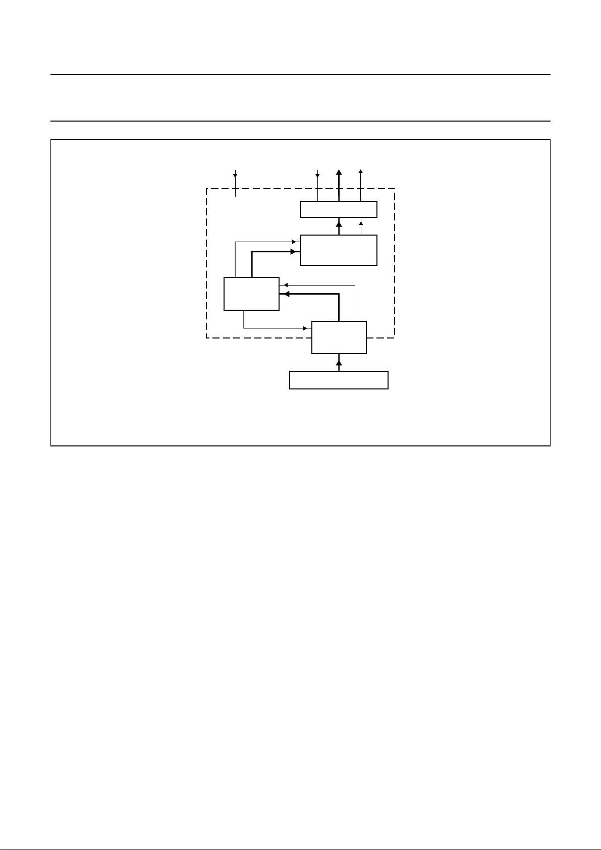
Philips Semiconductors Product specification
Multimedia bridge, high performance
Scaler and PCI circuit (SPCI)
handbook, full pagewidth
LLC
PXQ
DATA
DMA
READ
Dword request
DATA
VS
HS
D1 INTERFACE
FIFO empty
DATA
FIFO3
SAA7146A
PXQ
(write enable in line
memory mode)
BRS
PCI
MGG268
Fig.27 Sync and data path for direct and line memory mode.
7.10.3 VBI DATA INTERFACE
The SAA7146A transports VBI data (data during the
Vertical Blanking Interval) or VBI test signals between real
time world and the computer system. The data can be in
YUV format, luminance Y only, encoded digital CVBS on
luminance channel or a single bit stream of sliced data.
1 or 2 MSB of Y is utilized to carry ‘data bit’. PXQ pixel
qualifier is used as ‘data clock’.
7.11 Video data formats on the PCI-bus
The big/little-endian is supported in the way that a 2 and a
4-byte swapping is possible. The data formats using
32 bits per pixel requires a 4-byte swap, whereas the data
formats using 16 bits per pixel requires a 2-byte swap.
7.11.1 SCALER OUTPUT FORMATS (HPS)
7.11.1.1 RGB
RGB each defined as ‘full range’, all bits = 0 for black and
all bits = 1 for white. All RGB formats are composed
formats and use video FIFO 1 and video DMA Channel 1.
•αRGB-32: the αRGB format use a full byte for each
colour component and one byte for the colour key
information. The bytes are packed cyclicly into Dwords
and uses one Dword per sample. ‘α’ can be the colour
key bit in all 8 bits or read via FIFO 2 (see
Section 7.11.1.3) and uses one entire Dword per
sample (see Table 59).
• RGB-24 packed: The 24-bit RGB format use a full byte
for each colour component. The bytes are packed
cyclicly into Dwords, uses 0.75 Dwords per sample, i.e.
3 Dwords per 4 samples. The byte phase of the first
sample on each line is defined by the 2 LSBs of the DMA
base (see Table 60).
1998 Apr 09 80
Page 81
Philips Semiconductors Product specification
Multimedia bridge, high performance
Scaler and PCI circuit (SPCI)
Table 59 αRGB-32 format
PACKING WITHIN 32-BIT Dword
BIT 31 TO BIT 24 BIT 23 TO BIT 16 BIT 15 TO BIT 8 BIT 7 TO BIT 0
α/− RGB
α/−VYU
Table 60 RGB-24 packed format
BUS CYCLE
BIT 31 TO BIT 24 BIT 23 TO BIT 16 BIT 15 TO BIT 8 BIT 7 TO BIT 0
1B
2G
3R
1
2
3
The following formats use two pixels per Dword and derive
RGB from RGB-24 by truncation or by error diffusion
dither. The byte phase of the first sample each line is
defined by LSB + 1 of DMA base. ‘α’ is the colour key.
• RGB-16 (5:6:5): Red has 5 bits, Green has 6 bits,
Blue has 5 bits
• RGB-15 (α :5:5:5):α-bit, Red has 5 bits, Green has
5 bits, Blue has 5 bits
• RGB-15 (5:5:α: 5): Red has 5 bits, Green has 5 bits,
α bit, Blue has 5 bits.
Table 61 RGB-16 formats Dword
PACKING WITHIN 32-BIT Dword
BIT 31 TO BIT 16 BIT 15 TO BIT 0
Pixel
1
Pixel
0
PACKING WITHIN 32-BIT Dword
R
0
B
2
G
3
G
0
R
1
B
3
7.11.1.2 YUV
All YUV formats are based on CCIR coding:
Luminance Y in straight binary:
Black: Y = 16 of 256 linear coding
White: Y = 235 of 256 linear coding.
Colour difference signals UV in offset binary:
No colour: U = V = 128 of 256 steps
Full colour: U = V = 128 ±112 steps.
• YUV4:2:2: U and V sampled co-sided with first
Y sample (of 2 samples in-line). Byte phase of the first
sample each line is defined by bit 0 and bit 1 of DMA
base address (see Table 62).
• YUV4:1:1: U and V sampled co-sided with first
Y sample, (of 4 samples in-line), 8 samples are packed
in 3 Dwords (see Table 63).
SAA7146A
B
0
G
1
R
2
1998 Apr 09 81
Page 82
Philips Semiconductors Product specification
Multimedia bridge, high performance
SAA7146A
Scaler and PCI circuit (SPCI)
Table 62 YUV4:2:2 format
PACKING WITHIN 32-BIT Dword
BIT 31 TO BIT 24 BIT 23 TO BIT 16 BIT 15 TO BIT 8 BIT 7 TO BIT 0
Y
1
V
0
Table 63 YUV4:1:1 format
PACKING WITHIN 32-BIT Dword
BUS CYCLE
BIT 31 TO BIT 24 BIT 23 TO BIT 16 BIT 15 TO BIT 8 BIT 7 TO BIT 0
1Y
2Y
3Y
1
3
7
V
0
V
4
V
6
The following formats are planar YUV formats and use the three video FIFOs and three video DMA Channels 1, 2 and 3.
The byte phase of the first sample each line is defined by the 2 LSBs of every DMA base.
• YUV4:4:4; UandV sampled with every Y sample
• YUV4:2:2; UandV sampled co-sided with first Y sample (of 2 samples in-line)
• YUV4:2:0; MPEG U and V sampled at upper left sample of 4 sample in square (2 × 2)
• YUV-9 video; U and V sampled at selected sample of 16 samples in-square (4 × 4)
• YUV1; YUYV, YUYV...
• YUV2; YYUU, YYVV...
Y
0
Y
0
Y
2
Y
5
U
0
U
0
U
4
Y
4
7.11.1.3 8-bit formats
• Y8G; Only Y or inverted Y
•α8; 8-bit alpha information, to be master-read through FIFO 2 and merged into RGB-24 with alpha.
There are two pseudo CLUT formats, which derives its bits from RGB-24 or YUV-24 by truncation, or by error diffusion
dither. The byte phase of the first sample each field is defined by 2 LSBs of DMA base.
• RGB-8 (3 : 3 : 2); Red has 3 bits, Green has 3 bits, Blue has 2 bits
• YUV8 (4 : 2 : 2); Y has 4 bits, U has 2 bits, V has 2 bits. Y = 0 doesn’t exist, to handle 16-bit colour formats for pseudo
CLUT. After dithering, Y
min
=1.
All 8-bit formats are packed formats, 4 samples go into one Dword. The byte phase of the first sample of each line is
defined by the 2 LSBs of the DMA base. All except α8 use FIFO 1.
Table 64 8-bit formats
PACKING WITHIN 32-BIT Dword
BIT 31 TO BIT 24 BIT 23 TO BIT 16 BIT 15 TO BIT 8 BIT 7 TO BIT 0
pixel
3
pixel
2
pixel
1
pixel
0
1998 Apr 09 82
Page 83
Philips Semiconductors Product specification
Multimedia bridge, high performance
SAA7146A
Scaler and PCI circuit (SPCI)
7.11.2 BINARY RATIO SCALER OUTPUT FORMATS
All YUV formats are based on CCIR coding:
Luminance Y in straight binary:
Black: Y = 16 of 256 linear coding
White: Y = 235 of 256 linear coding.
Colour difference signals UV in offset binary:
No colour: U = V = 128 of 256 steps
Full colour: U = V = 128 ±112 steps.
The following formats use video FIFO 3, DMA Channel 3 and are packed formats.
• YUV4:2:2 UandV sampled co-sided with first Y sample (of 2 samples in-line). Byte phase of the first sample each
line is defined by bit 0 and bit 1 of DMA base address.
Table 65 YUV4:2:2 formats
PACKING WITHIN 32-BIT Dword
BIT 31 TO BIT 24 BIT 23 TO BIT 16 BIT 15 TO BIT 8 BIT 7 TO BIT 0
Y
1
V
0
Y
0
U
0
7.11.2.1 VBI data formats
• Y8; uses only the Y portion of the data stream and packs four bytes in one Dword
• YUV4:2:2; packs two pixel into one Dword, the order is Y1,V0,Y0,U
• 1-bit format; the Y1 format is a 1-bit format which packs 32 times the most significant bit of luminance (Y) into one
Dword, the first bit is bit 31 of the Dword
• 2-bit format; the Y2 format is a 2-bit format which packs 16 times the two most significant bits of luminance (Y) into
one Dword, the first bit is bit 31 of the Dword.
7.12 Scaler register
7.12.1 INITIAL SETTING OF DUAL D1 INTERFACE
The initial settings of the Dual D1 interface contains all control bits of the scaler part which do not change during a cyclic
processing of the video path. These control bits must be initialized at the beginning of the processing. The different
upload conditions of the video path depend on these control bits. Changing these bits during the active processing can
cause a valid UPLOAD.
0
1998 Apr 09 83
Page 84

Philips Semiconductors Product specification
Multimedia bridge, high performance
SAA7146A
Scaler and PCI circuit (SPCI)
Table 66 Initial setting of Dual D1 interface
OFFSET
(HEX)
50 LLC_A 31 RW Line Locked Clock control for D1_A:
50 SYNC_A 26 to 24 RW Sync edge selection and field detection mode internal sync signals SyncA
50 FIDESA 23 and22RW Field identification port_A edge select (ODD is defined by FID = 1, EVEN is
NAME BIT TYPE DESCRIPTION
0: LLC_A set to input
1: LLC_A set to output, taken from LLC_B
SIO_A 30 to 29 RW Synchronization port_A configuration:
00: HS_A and VS_A are input (i.e. 3-state)
01: HS_A is output, HGT of HPS; VS_A is output, VGT of HPS
10: HS_A is output, RESET signal for a field memory VS_A is input, vertical
sync signal for BRS this setting is needed for the field memory mode
11: HS_A is output, HGT of BRS; VS_A is output, VGT of BRS
PVO_A 28 RW Polarity of VS_A, if VS output:
0: direct from HPS or BRS, see SIO_A
1: inverted
PHO_A 27 RW Polarity of HS_A, if HS output is select by SIO_A:
0: direct from HPS or BRS, see SIO_A
1: inverted
(Ha, Va, Fa) if:
HS, VS are input: Ha/Va/Fa derived from pins
HS, VS are output: HS/VS as select by SIO_A
000: Ha at rising edge of HS; Va at rising edge of VS; Fa = HS × VS-rising,
directly
001: Ha at rising edge of HS; Va at falling edge of VS; Fa = Hs × VS-falling,
directly
010: Ha at rising edge of HS; Va at rising edge of VS; Fa = HS × VS-falling,
forced toggle
011: Ha at rising edge of HS; Va at falling edge of VS; Fa = HS × VS-falling,
forced toggle
100: Ha at rising edge of HS; Va at rising edge of VS; Fa = free toggle
101: Ha at rising edge of HS; Va at falling edge of VS; Fa = free toggle
110: Ha at rising edge of HS; Va at rising and falling edge of Frame Sync at
the VS pin; Fa = direct FS
111: Ha, Va, Fa; derived from SAV and EAV decoded from the data-stream
at D1_A port. Not used if the MSB of HPSdatasel in Table 71 is set to logic 1
defined by FID = 0)
00: no interrupt condition
01: rising edge is interrupt condition
10: falling edge is interrupt condition
11: both edges are interrupt condition
− 21 to 16 − reserved
1998 Apr 09 84
Page 85

Philips Semiconductors Product specification
Multimedia bridge, high performance
SAA7146A
Scaler and PCI circuit (SPCI)
OFFSET
(HEX)
50 LLC_B 15 RW Line Locked Clock control for D1_B:
50 SIO_B 14 and13RW Synchronization port_B configuration:
50 PVO_B 12 RW Polarity of VS_B, if VS output:
50 PHO_B 11 RW Polarity of HS_B, if HS output is select by SIO_B:
50 SYNC_B 10 to 8 RW Sync edge selection and field detection mode internal sync signals SyncB
50 FIDESB 7 and 6 RW Field identification port_B edge select (ODD is defined by FID = 1, EVEN is
NAME BIT TYPE DESCRIPTION
0: LLC_B set to input
1: LLC_B set to output, taken from LLC_A
00: HS_B and VS_B are input (i.e. 3-state)
01: HS_B is output, HGT of HPS; VS_B is output, VGT of HPS
10: HS_B is output, RESET signal for a field memory; VS_B is input, vertical
sync signal for BRS this setting is needed for the field memory mode
11: HS_B is output, HGT of BRS; VS_B is output, VGT of BRS
0: direct from HPS or BRS, see SIO_B
1: inverted
0: direct from HPS or BRS, see SIO_B
1: inverted
(Hb, Vb and Fb) if:
HS, VS are input: Hb/Vb/Fb derived from pins
HS, VS are output: HS/VS as select by SIO_B
000: Hb at rising edge of HS; Vb at rising edge of VS; Fb = HS × VS-rising,
directly
001: Hb at rising edge of HS; Vb at falling edge of VS; Fb = Hs × VS-falling,
directly
010: Hb at rising edge of HS; Vb at rising edge of VS; Fb = HS × VS-falling,
forced toggle
011: Hb at rising edge of HS; Vb at falling edge of VS; Fb = HS × VS-falling,
forced toggle
100: Hb at rising edge of HS; Vb at rising edge of VS
101: Hb at rising edge of HS; Vb at falling edge of VS; Fb = free toggle
110: Hb at rising edge of HS; Vb at rising and falling edge of Frame Sync at
the VS pin; Fb = direct FS
111: Hb, Vb and Fb derived from SAV and EAV decoded from the
data-stream at D1_B port. Not used if the MSB of HPSdatasel in Table 71
is set to logic 1
defined by FID = 0)
00: no interrupt condition
01: rising edge is interrupt condition
10: falling edge is interrupt condition
11: both edges are interrupt condition
− 5to0 − reserved
1998 Apr 09 85
Page 86

Philips Semiconductors Product specification
Multimedia bridge, high performance
SAA7146A
Scaler and PCI circuit (SPCI)
7.12.2 VIDEO DATA STREAM HANDLING AT PORT D1_A
Table 67 Video data stream handling at port D1_A
OFFSET
(HEX)
54 VID_A 31 and 30 RW Video data Port_A and PXQ_A select (PXQ goes always with data):
NAME BIT TYPE DESCRIPTION
00: input, i.e. 3-state
01: reserved
10: output data stream is Y8C from BRS
11: output data stream is Y8C from HPS
Y8C_A 29 RW Y8C codes, if output Y8C only:
0: no SAV and EAV data in the video data output-stream
1: with SAV and EAV
− 28 and 27 − reserved
PFID_A 26 RW Polarity change of the field identification signal at Port_A:
0: as detected in the field detection
1: inverted
− 25 to 16 − reserved
7.12.3 V
Table 68 Video data stream handling at port D1_B
OFFSET
(HEX)
IDEO DATA STREAM HANDLING AT PORT D1_B
NAME BIT TYPE DESCRIPTION
54 VID_B 15 and 14 RW Video data Port_B and PXQ_B select (PXQ goes always with data):
00: input, i.e. 3-state
01: reserved
10: output data stream is Y8C from BRS
11: output data stream is Y8C from HPS
Y8C_B 13 RW Y8C codes:
0: no SAV and EAV data in the video data output stream
1: with SAV and EAV
− 12 and 11 − reserved
PFID_B 10 RW Polarity change of the field identification signal at Port_B
0: as detected in the field detection
1: inverted
− 9to0 − reserved
1998 Apr 09 86
Page 87

Philips Semiconductors Product specification
Multimedia bridge, high performance
SAA7146A
Scaler and PCI circuit (SPCI)
7.12.4 BRS PROGRAMMING REGISTER
The BRS programming has in principle three modes:
1. Inbound and downscaling: the binary ratio scaler input multiplexer selects data from the Dual D1 real time video
interface, Port A or B and ‘normally’ writes the result via FIFO 3 and DMA3 to PCI, if DMA3 is enabled in master write
mode and not used for other purposes. Syncs including Field ID are taken from Port A or B (FID defines which base
address is used in DMA3).
2. Outbound and upscaling in direct and line memory mode: the binary ratio scaler takes the data from FIFO 3.
The DMA3 is in master read operation. The scaling result can be selected by the DD1 port output multiplexers.
The timing reference signals (VS, HS, LLC and FID) are taken from Port A or B.
3. Outbound and upscaling in field memory mode: the binary ratio scaler takes the data from FIFO 3. The DMA3 is
in master read operation. The scaling result can be selected by the DD1 port output multiplexers. The vertical sync
signal is taken from the VS_A or VS_B port as timing reference signal. At the HS_A or HS_B port the SAA7146A
generates a reset signal for each field. The PXQ is an output signal which is connected to the write enable port of
the memory. If an interlaced source is selected (different base addresses for ODD and EVEN fields), the field
detection must be set to ‘free toggle’ mode, due to the missing horizontal sync signal.
Table 69 BRS control register
OFFSET
(HEX)
58 BRSdatasel
NAME BIT TYPE
and MODE
BRSsyncsel 29 RW source select for BRS sync signals:
BYO 28 to 19 RW vertical offset, counted in lines,
BRS_V 18 and 17 RW vertical downscaling: vertical upscaling:
INBOUND OUTBOUND
31 and 30 RW source select for BRS video data:
00: video data stream from A 11: read from DMA_3/FIFO 3
01: video data stream from B
10: reserved
0: take Ha, Va, Fa, LLC_A as
select in the ‘Initial setting of
Dual D1 Interface’;
see Table 66.
1: take Hb, Vb, Fb, LLC_B as
select in the ‘Initial Setting of
Dual D1 Interface’;
see Table 66.
after selected vertical sync edge
until data is captured from DD1
00: write every line to DMA3 00: regular read
01: write every 2nd line only 01: read every line twice
10: reserved 10: reserved
11: write every 4th line only 11: read every line 4 times
DESCRIPTION
in direct and line memory mode
the same setting as in the
inbound mode is select
in field memory mode the
horizontal sync port must set to
output to get the a field RESET
signal for a field memory
BYO defines a vertical offset,
counted in lines, after selected
vertical sync-edge until data is
read from the FIFO. For field
memory mode BYO must be
000H. The video window is
selected by ‘NumLines’,
‘NumBytes’, ‘pitch’ and ‘base
address’.
1998 Apr 09 87
Page 88

Philips Semiconductors Product specification
Multimedia bridge, high performance
Scaler and PCI circuit (SPCI)
OFFSET
(HEX)
58 BXO 16 to 7 RW horizontal offset, counted in
NAME BIT TYPE
INBOUND OUTBOUND
qualified LLC cycles, after
selected horizontal sync edge, till
data is captured from DD1
BRS_H 6 to 4 RW horizontal downscaling
(see Section 7.10.1):
000: every pixel is captured 000: provide every sample once
001: every 2nd pixel is captured 001: provide every sample
010: reserved 010: reserved
011: every 4th pixel is captured 011: provide every sample
100: reserved 100: reserved
101: reserved 101: reserved
110: reserved 110: reserved
111: every 8th pixel is captured 111: provide every sample
Read mode 3 and 2 RW reserved 00: line memory mode
PCI format 1 and 0 RW output format PCI side: input format PCI side:
00: YUV4:2:2 00: YUV4:2:2
01: Y8, only luminance 01: reserved
10: Y2, 2 MSBs of Y only 10: reserved
11: Y1, 1 MSB of Y only 11: reserved
SAA7146A
DESCRIPTION
BXO defines a horizontal offset,
counted in LLC cycles, after
selected horizontal sync edge till
data is read from the FIFO
in field memory mode the
following offsets depending on the
horizontal scaling ratio must be
selected to guarantee the correct
outrun behaviour of the scaler
(see Table 70). The video
window is select by ‘NumLines’,
‘NumBytes’, ‘pitch’ and ‘base
address’
horizontal upscaling:
twice
4 times
8 times
01: field memory mode
10: direct mode with pixel
repetition for not qualified bytes.
11: direct with grey pixel (10H
for luminance and 80H for
chrominance values) for not
qualified bytes.
1998 Apr 09 88
Page 89

Philips Semiconductors Product specification
Multimedia bridge, high performance
Scaler and PCI circuit (SPCI)
Table 70 Horizontal offset values for the field memory mode
RATIO OFFSET
1 0CH
2 0CH
4 16H
8 2EH
7.12.5 HPS
Table 71 HPS control register
OFFSET
(HEX)
5C HPSdatasel 31 and 30 RW source select for HPS video data:
PROGRAMMING REGISTER
NAME BIT TYPE DESCRIPTION
00: input video stream for HPS is taken from Port_A
01 input video stream for HPS is taken from Port_B
10: Y-byte from Port_B, C-byte from Port_A (CREF must provide at
Port_A)
11: Y-byte from Port_A, C-byte from Port_B (CREF must provide at
Port_B)
Mirror 29 RW left-right flip (mirroring), e.g. for vanity picture:
0: regular processing
1: left-right flip, accessible only if XT (number of pixel after horizontal
prescaling) is less than 384 pixels
HPSsyncsel 28 RW source select for HPS sync-signals:
0: take Ha, Va, Fa, LLC_A as selected in Table 66
1: take Hb, Vb, Fb, LLC_B, as selected in Table 66
− 27 to 24 RW reserved
HYO 23 to 12 RW vertical offset (start line) of HPS operation, counted in horizontal
source/input events, after selected vertical sync edge
− 11 to 0 RW reserved
SAA7146A
1998 Apr 09 89
Page 90

Philips Semiconductors Product specification
Multimedia bridge, high performance
SAA7146A
Scaler and PCI circuit (SPCI)
7.12.6 VERTICAL AND HORIZONTAL SCALING
Table 72 HPS, vertical scaling
OFFSET
(HEX)
60 YACM 31 RW Y (vertical) scaler Accumulation (calculation) Mode of vertical
NAME BIT TYPE DESCRIPTION
arithmetic:
0: arithmetic operates as a linear phase interpolation (LPI)
1: arithmetic operates as accumulating FIR filter in vertical
direction.
YSCI 30 to 21 RW Y scaler increment for vertical downscaling:
YSCI = INT [1024 × (N
YSCI = INT [1024 × (1 − N
YACM = 1 → accumulation mode
N
= number of qualified scaler input lines
IL
N
= number of output lines
OL
YACL 20 to 15 RW accumulation sequence Length of the Y (vertical) processing:
Defines vertical accumulation sequence length of input lines
If accumulation FIR filter mode is selected YACM, YACL has to
fit to the vertical scaling factor (defined by YSCI)
YPO 14 to 8 RW vertical start phase for vertical scaling of the ODD field:
YPO = PHOL × 128
(PHOL represents a phase offset with values between logic 0
and logic 1, where the logic 1 represents a distance between two
consecutive lines of the input pattern)
YPE 7 to 1 RW vertical start phase for vertical scaling of the EVEN field:
YPE = PHOL × 128
(PHOL represents a phase offset with values between logic 0
and logic 1, where the logic 1 represents a distance between two
consecutive lines of the input pattern).
− 0 RW reserved
− 1) for YACM = 0 → LPI
IL/NOL
)] for
OL/NIL
1998 Apr 09 90
Page 91
Philips Semiconductors Product specification
Multimedia bridge, high performance
Scaler and PCI circuit (SPCI)
Table 73 HPS, vertical scale and gain
OFFSET
(HEX)
64 PFY 31 to 28 RW prefilter selection for luminance component Y:
NAME BIT TYPE DESCRIPTION
H(z) = H1(z) × H2(z) × H3(z)
H1, H3 = 1 + z
H2=1+A×z−1+z
−1
−2
see Table 74
PFUV 27 to 24 RW prefilter selection for colour difference signals UV:
H(z) = H1(z) × H2(z) × H3(z)
H1=1+z
H2=1+A×z−1+z
H3=1+z
−1
−2
−2
see Table 75
− 23 to 19 − reserved
DCGY 18 to 16 RW DC gain control of Y scaler:
Dependent on active coefficients and the sequence length, the
amplitude gain has to be renormalized.
Gain factor = 2 (DCGY + 1); see Table 76. The resulting factor is a
function of CYi and DCGY. The resulting weight factor = 0 for
CYAi = CYBi = 0 or CYAi= CYBi = 1 or DCGY >5 otherwise
weight = weighting factor/gain factor; see Table 77.
CY A 15 to 8 RW Coefficient select for Y (vertical) processing in accumulation mode.
CYB 7 to 0 RW
For improvement of vertical filtering the accumulated lines can be
weighted. Weighting factor = 2(2 × CYBi + CY Ai − 1); see T able 78.
SAA7146A
Table 74 Prefilter selection for luminance component Y
PFY1 PFY0 PFY1 PFY0 H1 H2 H3 A
X X 0 0 bypass bypass bypass X
X X 0 1 active bypass bypass X
X X 1 0 active bypass active X
0011active active active 2
0111active bypass bypass
1011active bypass active
1111active active active
1998 Apr 09 91
15
⁄
16
7
⁄
8
3
⁄
4
Page 92
Philips Semiconductors Product specification
Multimedia bridge, high performance
SAA7146A
Scaler and PCI circuit (SPCI)
Table 75 Prefilter selection for colour difference signals UV
PFY1 PFY0 PFY1 PFY0 H1 H2 H3 A
X X 0 0 bypass bypass bypass X
X X 0 1 active bypass bypass X
X X 1 0 active bypass active X
0011active active active 2
0111active bypass bypass
1011active bypass active
1111active active active
Table 76 DC gain control of Y scaler
DCGY2 DCGY1 DCGY0 DCGY GAIN FACTOR
00002
00114
01028
011316
100432
101564
1106128
1117256
15
⁄
16
7
⁄
8
3
⁄
4
Table 77 Weight factor as a function of CYi and DCGY
DCGY
CYi
01234567
000000000
1
1
⁄
2
21
1
⁄
4
1
⁄
2
301
1
⁄
8
1
⁄
4
1
⁄
2
1
⁄
16
1
⁄
8
1
⁄
4
1
⁄
32
1
⁄
16
1
⁄
8
1
⁄
64
1
⁄
32
1
⁄1600
00
00
Table 78 Coefficient select for Y (vertical) processing in accumulation mode
CYBi CYAi CYi WEIGHTING FACTOR
0000
0111
1022
1134
1998 Apr 09 92
Page 93
Philips Semiconductors Product specification
Multimedia bridge, high performance
Scaler and PCI circuit (SPCI)
Table 79 HPS, horizontal prescaler
OFFSET
(HEX)
68 − 31 and 30 − reserved
NAME BIT TYP. DESCRIPTION
DCGX 29 to 27 RW DC gain control of X prescaler (see T able 57): depending on the
− 26 to 24 − reserved
XPSC 23 to 18 RW prescaling factor of the X PreSCaler: defines accumulation
XACM 17 RW X (horizontal) prescaler Accumulation Mode of accumulating
− 16 − reserved
CXY 15 to 8 RW Coefficient select for X prescaler (luminance component Y):
CXUV 7 to 0 RW Coefficient select for X prescaler (colour difference signals
SAA7146A
number of active coefficients ‘2’ in the accumulation sequence and
the sequence length, the output amplitude gain has to be set to as
given in Table 80.
sequence length and subsampling factor of the input data stream:
XPSC = TRUNC (N
N
= number of prescaler output pixel
OP
N
= number of qualified scaler input pixel.
IP
IP/NOP
FIR:
0: accumulating operates overlapping
1: non overlapping accumulation (must be set to bypass the
prescaler).
for DC gain compensation of prescaler the accumulated pixels can
be weighted by ‘1’ or ‘2’. CXYi defines a sequence of 8 bits, which
control the coefficients:
CXYi = 0: pixel weighted by ‘1’
CXYi = 1: pixel weighted by ‘2’
UV): for DC gain compensation of prescaler the accumulated
pixels can be weighted by ‘1’ or ‘2’. CXUVi defines a sequence of
8 bits, which control the coefficients:
CXUVi = 0: pixel weighted by ‘1’
CXUVi = 1: pixel weighted by ‘2’
− 1)
Table 80 Selection of output gain
DCGX2 DCGX1 DCGX0 GAIN
0001
001
010
011
100
101
110
111
1998 Apr 09 93
1
⁄
2
1
⁄
4
1
⁄
8
1
⁄
2
1
⁄
4
1
⁄
8
1
⁄
16
Page 94
Philips Semiconductors Product specification
Multimedia bridge, high performance
Scaler and PCI circuit (SPCI)
Table 81 HPS, horizontal fine-scale
OFFSET
(HEX)
6C XIM 31 RW horizontal interpolation mode:
NAME BIT TYP. DESCRIPTION
0: normal mode, sample phase is calculated for every qualified
sample
1: fixed phase, sample phase is fixed to the value set by XP
XP 30 to 24 RW start phase for horizontal fine scaling XP = PHO
(PHOP represents a phase offset with values between ‘0’ and ‘1’,
where the ‘1’ represents a distance between two consecutive
pixels of the input pattern)
XSCI 23 to 12 RW X Scaler Increment for fine (phase correct) scaling in
horizontal pixel phase arithmetic:
XSCI = INT [(N
= number of output pixels
N
OP
N
= number of qualified scaler input pixels.
IP
HXO 11 to 0 RW horizontal offset (horizontal start) of input source for HPS, counted
in qualified pixels with PXQ, after selected horizontal sync edge.
IP/NOP
) × 1024/(SPSC + 1)]
SAA7146A
× 128
P
7.12.7 BCS
Table 82 BCS control
OFFSET
(HEX)
70 BRIG 31 to 24 RW luminance brightness control; see Table 83
Table 83 Luminance brightness control
D7 D6 D5 D4 D3 D2 D1 D0 GAIN
11111111255(bright)
10000000128(CCIR level)
000000000(dark)
Table 84 Luminance contrast control
D7 D6 D5 D4 D3 D2 D1 D0 GAIN
011111111.999 (max. contrast)
010000001(CCIR level)
000000000(luminance off)
NAME BIT TYPE DESCRIPTION
CONT 23 to 16 RW luminance contrast control; see Table 84
− 15 to 8 − reserved
SATN 7 to 0 RW chrominance saturation control; see Table 85
1998 Apr 09 94
Page 95

Philips Semiconductors Product specification
Multimedia bridge, high performance
SAA7146A
Scaler and PCI circuit (SPCI)
Table 85 Chrominance saturation control
D7 D6 D5 D4 D3 D2 D1 D0 GAIN
011111111.999 (max. saturation)
010000001(CCIR level)
000000000(colour off)
7.12.8 C
Table 86 Chroma key range
OFFSET
(HEX)
HROMA KEY
NAME BIT TYPE DESCRIPTION
74 VL 31 to 24 RW set lower limit V for chroma keying (8-bit; twos complement):
1000 0000: as maximum negative value = −128 signal level
0000 0000: limit = 0
0111 1111: as maximum positive value = +127 signal level
VU 23 to 16 RW set upper limit V for chroma keying (8-bit; twos complement):
1000 0000: as maximum negative value = −128 signal level
0000 0000: limit = 0
0111 1111: as maximum positive value = +127 signal level
UL 15 to 8 RW set lower limit U for chroma keying (8-bit; twos complement):
1000 0000: as maximum negative value = −128 signal level
0000 0000: limit = 0
0111 1111: as maximum positive value = +127 signal level
UU 7 to 0 RW set upper limit U for chroma-keying (8-bit; twos complement):
1000 0000: as maximum negative value = −128 signal level
0000 0000: limit = 0
0111 1111: as maximum positive value = +127 signal level
1998 Apr 09 95
Page 96
Philips Semiconductors Product specification
Multimedia bridge, high performance
Scaler and PCI circuit (SPCI)
Table 87 HPS output and formats
OFFSET
(HEX)
78 matrix 31 and 30 RW YUV to RGB conversion, gamma compensation
NAME BIT TYPE DESCRIPTION
00: no YUV to RGB conversion 10: YUV to RGB conversion
01: reserved 11: YUV to RGB conversion
− 29 and 28 − reserved
outformat 27 to 24 RW output format, depends on matrix programming; see Table 88
23 and 22 RW chroma line select for INDEO-9
21 and 20 RW chroma pixel select for INDEO-9
SHIFT 17 RW 0: normal mode, all bytes stay MSB aligned
1: shift mode, ‘shift right’ of all bytes, fill MSB position with logic 0,
this mode has meaning only for output formats defined in bytes,
undefined result in non-byte modes
DITHER 16 RW dither: applies only to formats with reduced bit resolution, (#) that
derived from higher bit resolution formats:
1: dither is applied by ‘linear’ one-dimensional error diffusion
0: dither algorithm is not applied, just truncation
SAA7146A
linear
with compensation of
gamma-pre-correction
Table 88 Output formats
CODE (HEX) OUTPUT FORMAT
0 YUV4:2:2, (16=8−8), composed RGB16 (5:6:5), composed, #
1 YUV4:4:4, composed, ‘packed’ RGB24, composed, ‘packed’
2 reserved αRGB32 (8 : 8 : 8 : 8), composed
3 YUV4:1:1, composed αRGB15 (1 : 5 : 5 : 5), composed, #
4 YUV2 RGαB15 (5 : 5 : 1 : 5), composed, #
5 reserved reserved
6 Y8, monochrome reserved
7 YUV8 (4:2:2), pseudo CLUT, # RGB8 (3:3:2), pseudo CLUT, #
8 YUV4:4:4, de-composed reserved
9 YUV4:2:2, de-composed reserved
A YUV4:2:0 (2
B YUV9 (4
C reserved reserved
D Y1 reserved
E Y2 reserved
F YUV1 reserved
2
:1:1) MPEG, de-composed. reserved
2
:1:1) INDEO-9, de-composed. reserved
1998 Apr 09 96
Page 97

Philips Semiconductors Product specification
Multimedia bridge, high performance
Scaler and PCI circuit (SPCI)
Table 89 Clip control
OFFSET NAME BIT TYPE DESCRIPTION
78H − 15 to 10 − reserved
ClipCK 9 and 8 RW clipping by chroma key CK (or MSB of α-8): OR-ed with other clip
list or clip-bit mask, if ClipMode is enabled
00: chroma key CK is not used for clipping, CK →α
01: chroma key CK is not used for clipping, inverted CK →α
10: clipping, based on chroma key CK bit
11: clipping, based on chroma key CK bit inverted
− 7 − reserved
ClipMode 6 to 4 RW clipping based on DMA2 read information: OR-ed with chroma
key CK, if ClipCK is enabled
000: no clipping based on DMA2 read, DMA2 can be used to write
decomposed format U
001: no clipping based on DMA2 read; DMA2 reads 8-bit-α to
substitute CK in α-formats
010: reserved
011: reserved
100: clipping, based on pixel clip list, rectangular overlays
101: clipping, based on pixel clip list, rectangular overlays,
inverted
110: clipping, based on pixel clip bit mask 1-bit/pixel
111: clipping, based on pixel clip bit mask 1-bit/pixel, inverted
RecInterl 3 RW select interlaced mode for rectangular overlays:
0: normal mode
1: interlaced mode, this bit must be set if only one clip list for both
fields is available. This function assumes that the ODD field is
always above the EVEN field.
− 2 − reserved
ClipOut 1 and 0 RW use of DMA3 to report (write) key of clip information back:
00: no clip output, DMA3 can be used to write decomposed format
V, or to serve BRS, read or write
01: DMA3 writes chroma key information CK; 1-bit/pixel
10: DMA3 writes back (clip mask-CK); 1-bit /pixel
11: DMA3 writes applied pixel clipping back; 1-bit/pixel
SAA7146A
7.13 Scaler event description
The RPS is controlled by the PAUSE command on special
events. This section describes the video events. Because
of these video events a defined time for an upload is given.
Table 90 shows the UPLOAD handling for the scaler
registers. For special applications it can also be useful to
select other combinations. For this the termination of the
UPLOAD must guarantee that the UPLOAD is completed
before the processing restarts, e.g. with a new line or a
1998 Apr 09 97
new field. To avoid conflicts, e.g. change of vertical
settings during vertical processing, the MASKWRITE
command can be used to change single bits within a
Dword. Each video event can force only one upload at a
time. This means that the video event is cleared by the
circuit as described below, if the corresponding upload has
occurred.
Page 98

Philips Semiconductors Product specification
Multimedia bridge, high performance
SAA7146A
Scaler and PCI circuit (SPCI)
Table 90 UPLOAD handling for the scaler registers
REGISTER
Initial setting of Dual
D1 Interface
Video DATA stream
handling at port D1_A
Video DATA stream
handling at port D1_B
BRS control register 58 BRS_DONE Inactive BRS data path: in write mode the BRS data path is
HPS control 5C HPS_DONE Inactive HPS data path between two video windows: the
HPS vertical scale 60
HPS vertical scale
and gain
Chroma key range 74
HPS output and
formats
Clip control 78
HPS, horizontal
prescale
HPS, horizontal
fine-scale
BCS control 70
OFFSET
(HEX)
50 no video event The ‘initial settings of the Dual D1 interface’ contains all
54 VBI_A Vertical Blanking Indicator at VS_A port: the VBI is a
54 VBI_B Vertical Blanking Indicator at VS_B port: the VBI is a
64
78
68 HPS_LINE_DONE Inactive HPS data path between two lines: The HPS data
6C
VIDEO EVENT DESCRIPTION
control bits of the scaler part which do not change during a
cyclic processing of the video path. These control bits must
be initialized at the start of the processing. The different
upload conditions of the video path depend on these control
bits. Changing these bits during the cyclic processing can
cause internal pulse signals which generate video events.
These events may not fit into the sequence for the cyclic
processing.
V-pulse which depends on the selected edge of the vertical
blanking interval. The edge is defined by the SYNC_A bits.
The selected mode depends on the accepted sync signals.
This register can be uploaded with this V-pulse.
V-pulse which depends on the selected edge of the vertical
blanking interval. The edge is defined by the SIO_B bits.
The selected mode depends on the accepted sync signals.
This register can be uploaded with this V-pulse.
inactive from the falling edge of VGT at the output of the
BRS which means that target line and target byte are
reached to the start of the next field (V-pulse which triggered
the BRS acquisition). For the read mode this register
contains only initial settings which can not change during
cyclic processing.
HPS data path is inactive from the falling edge of the VGT at
the output of the HPS, indicating that target line and target
byte are reached, to the start of the next window
processing. V-pulse at the HPS acquisition input.
path is inactive from the falling edge of the HGT at the
output of the HPS, indicating that target byte are reached to
the start of the next line processing. Rising edge of the HGT
at the HPS acquisition output.
1998 Apr 09 98
Page 99

Philips Semiconductors Product specification
Multimedia bridge, high performance
Scaler and PCI circuit (SPCI)
7.14 Clipping
The SAA7146A supports clipping in the HPS data path.
Clipping can be achieved with the chroma key information
or with clip data information coming via master read
through FIFO 2. Both sources will be OR-ed and can be
switched on/off or inverted individually. These settings are
controlled by the registers ClipCK and ClipMode.
The information read via FIFO 2 can be used for clipping
with rectangular overlays or for bit mask clipping.
The overlay clipping supports up to 16 rectangular
overlays using 64 Dwords. The bit mask clipping allows an
arbitrary number of window clips of any size or shape. This
mode needs one bit for every pixel.
Chroma or clip information can be written to system
memory via FIFO 3. This is controlled by the ClipOut
register. It is possible to combine the clip information with
the inversion of the applied (foreground) chroma key.
The result is a mask leaving the (background) area free.
This mask can be read back in the next field to clip a
different video stream to be placed into the same window
as background (blue boxing).
It should be noted that planar output formats overrule the
use of FIFO 2 and FIFO 3 for clipping. Only chroma
clipping is available and no clip information can be written.
7.14.1 B
The bit mask clipping will use one Dword as clip data for
32 pixels. The first bit of clip data is the MSB.
7.14.2 R
The rectangular overlay clipping is responsible for
occluding rectangular overlay windows lying over a video
window.
The rectangular clipping algorithm needs two lists; one for
pixels and one for lines. Every list element in both lists
contains a coordinate and display information for every
overlay window. The 64 Dword FIFO 2 allows up to
16 overlay windows, each having two pixel list entries and
two line list entries.
The rectangular overlay clipping can be used in interlaced
or non-interlaced mode. This is controlled by the
‘RecInterl’ register bit. The overlay window coordinates are
defined for the target window, independent of whether the
video will be written interlaced or non-interlaced into the
target window.
Every overlay window is defined by its top/left and
bottom + 1/right + 1 coordinates. The coordinates are
relative to the top left (0, 0) reference of the video window.
IT MASK CLIPPING
ECTANGULAR OVERLAY CLIPPING
SAA7146A
The overlay clipping combines the coordinates with
display information which is a ‘overlay/no_overlay’
(1, 0) bit for each overlay window. A simple example,
shown in Fig.28, illustrates the relationship between
coordinates and display information.
In this example one overlay window ‘a’ (5, 1; 8, 3) is
defined. Relevant coordinates for the algorithm are the
coordinates where display information changes. At the
top/left coordinates (5, 1) the display information will be set
to 1 (‘overlay’). Therefore, first list entries are (5, 1) for the
pixel list and (1, 1) for the line list. The overlay will end at
the bottom/right coordinates plus one, e.g. at (9, 4)
(8 + 1, 3 + 1). This will lead to the list entries (9, 0) for the
pixel list and (4, 0) for the line list.
The central element of the rectangular overlay clipping
combines the display information of lines and pixels held in
the registers PIXEL_INFO and LINE_INFO. This unit will
provide the ‘no_display’ information when both line and
pixel display information are set to ‘no_display’. In the
example shown in Fig.28, this will happen for the pixels
5 to 8 and for the lines 1 to 3.
If there is more than one overlay window, the window
display information of all windows will be combined into
one display information. If any of the display information of
any window is indicated ‘no_display’ the actual pixel will
not be displayed. This ensures that overlapping overlay
windows will be handled by the hardware, since the video
information will only be displayed when no window is lying
over it. Since the overlapping information is only implicitly
in the lists, the overlapping information need not be taken
into account during the creation of the lists.
The main part of the algorithm is responsible for loading
the display information registers PIXEL_INFO and
LINE_INFO. Both will be initialized to ‘display’. LINE_INFO
will be updated at the beginning of every line, when the line
counter is equal to the LINE_NR in the line list.
PIXEL_INFO will be updated when the pixel counter is
equal to the PIXEL_NR in the pixel list. If there is no new
information both registers will hold their old values.
Both line and pixel list have to be sorted from top to bottom
or left to right coordinates and are not allowed to have two
consecutive list elements with the same coordinate. In the
example shown in Fig.29, the list entry with line
coordinate 1 will hold the ‘display’ information of window
‘a’ and the ‘no_display’ information of window ‘c’, so two
list elements with the same coordinate are merged into
one. The last elements in the lists are characterized by the
coordinate 0.
1998 Apr 09 99
Page 100
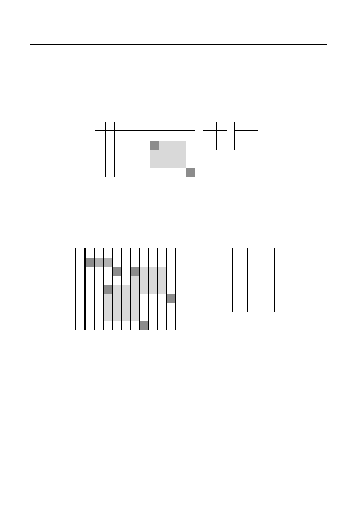
Philips Semiconductors Product specification
Multimedia bridge, high performance
Scaler and PCI circuit (SPCI)
handbook, full pagewidth
0
1
2
3
4
123456789
0
aaaa
aaaa
aaaa
Fig.28 Example 1 - Rectangular overlay clipping.
pixel
51
9
Relevant coordinates shaded dark
a
0
line
a
11
0
4
MGG267
SAA7146A
handbook, full pagewidth
0
ccc
0
1
2
3
4
5
6
7
123456789
aaaa
aaaa
aaa
bbbb
bbbb
bbbb
bbbb
pixel
0 110
2
3
5
6
9
0
Relevant coordinates shaded dark
bc
a
100
101
001
011
111
xxx
line
0 110
1
3
4
7
0
bc
a
011
001
101
111
xxx
MGG269
Fig.29 Example 2 - Rectangular overlay clipping.
7.14.2.1 Memory organization for rectangle overlay windows.
Every overlay window is defined by two corners with four coordinates. One Dword holds one 11-bit coordinate and 16-bit
with the display information for up to 16 overlay windows.
Table 91 Dword organization for rectangular overlay windows
UNUSED COORDINATE DISPLAY INFO
bit 31 to bit 27 (5-bit) bit 26 to bit 16 (11-bit) bit 15 to bit 0 (16-bit)
1998 Apr 09 100
 Loading...