

Page 1
INTEGRATED CIRCUITS
DATA SH EET
SAA7140A; SAA7140B
High Performance Scaler (HPS)
Objective specification
Supersedes data of 1996 Jul 26
File under Integrated Circuits, IC22
1996 Sep 04
Page 2

Philips Semiconductors Objective specification
High Performance Scaler (HPS) SAA7140A; SAA7140B
CONTENTS
1 FEATURES
2 GENERAL DESCRIPTION
3 ORDERING INFORMATION
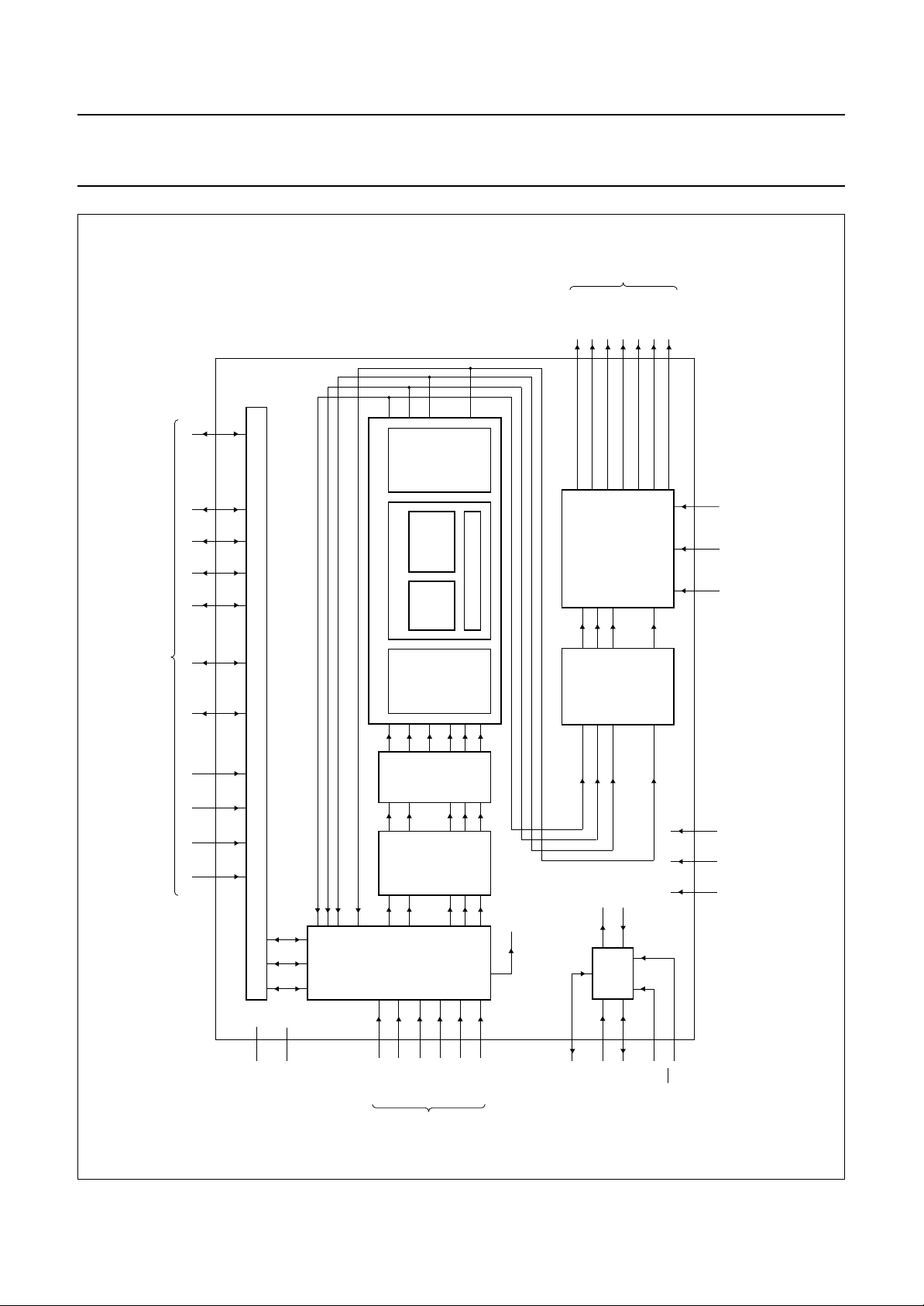
4 BLOCK DIAGRAM
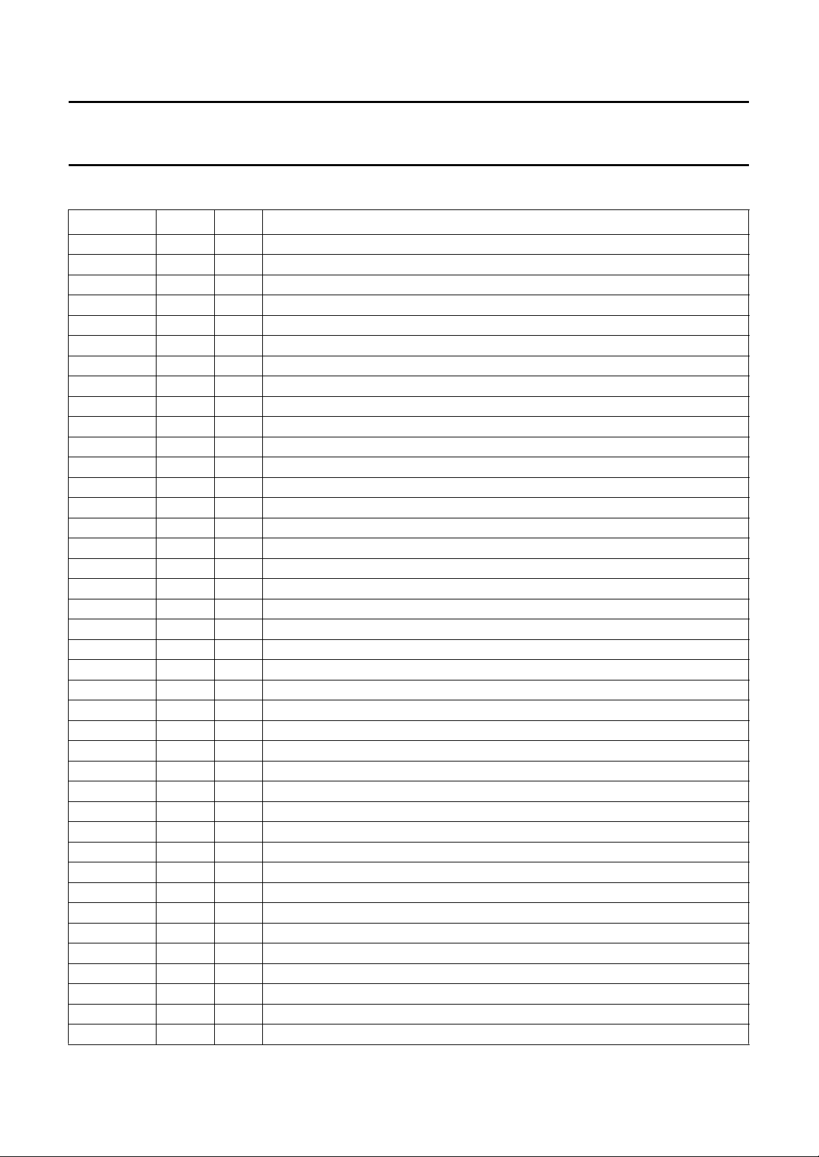
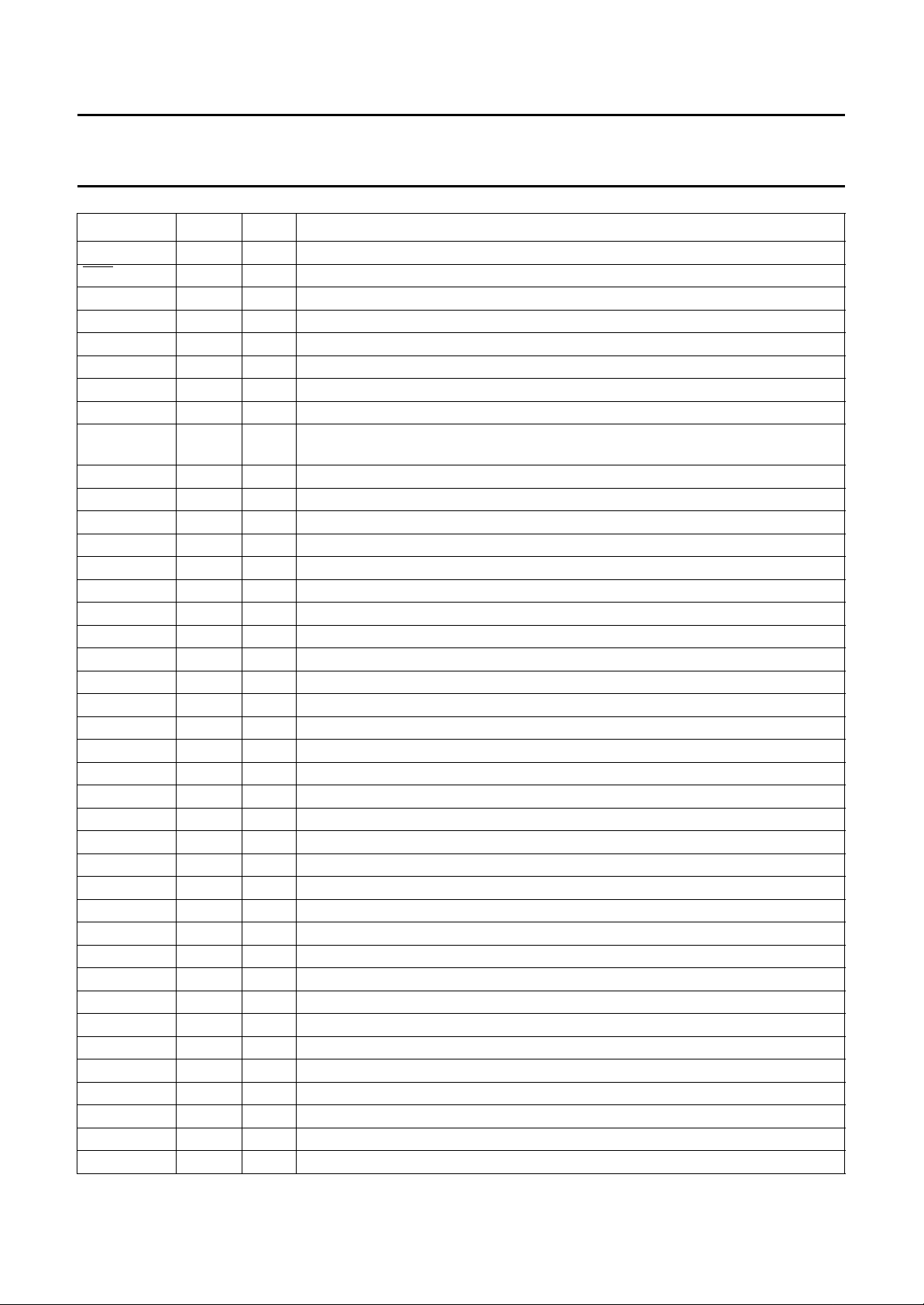
5 PINNING (SAA7140A)
6 PINNING (SAA7140B)
7 FUNCTIONAL DESCRIPTION
7.1 Data format/reformatter and reference signal
generation
7.1.1 Data formats and reference signals of the
DMSD port
7.1.2 Data formats and reference signals of the
expansion port
7.2 Acquisition control
7.3 BCS control
7.4 Scaling unit
7.4.1 Horizontal prescaling
7.4.2 Vertical scaler
7.4.3 Horizontal variable phase scaling
7.5 CSM (Colour Space Matrix), dither and gamma
correction
7.6 Output formatter and output FIFO register
7.6.1 Data formats and reference signals of the
VRAM port
7.7 Data transfer modes
7.7.1 Expansion port modes
7.8 VRAM port modes
7.8.1 Data burst transfer mode (FIFO Mode)
7.8.2 Continuous data transfer mode (transparent
mode)
7.8.3 I2C-bus controlled pseudo sleep mode
8I
8.1 I2C-bus format
8.2 I2C-bus bitmap
8.3 Description of the I2C-bus bits
8.3.1 Initial settings for the expansion and DMSD
8.3.2 Initial settings for the VRAM port;
8.3.3 Port I/O control; subaddress 21H
8.3.4 Register set A (02H to 1FH) and B
9 LIMITING VALUES
10 HANDLING
11 THERMAL CHARACTERISTICS
12 DC CHARACTERISTICS
13 AC CHARACTERISTICS
2
C-BUS PROTOCOL
port; Subaddress 00H
subaddress 01H
(22H to 3FH)
14 PACKAGE OUTLINE
15 SOLDERING
15.1 Introduction
15.2 Reflow soldering
15.3 Wave soldering
15.3.1 QFP
15.3.2 SO
15.3.3 Method (QFP and SO)
15.4 Repairing soldered joints
16 DEFINITIONS
17 LIFE SUPPORT APPLICATIONS
18 PURCHASE OF PHILIPS I2C COMPONENTS
1996 Sep 04 2
Page 3

Philips Semiconductors Objective specification
High Performance Scaler (HPS) SAA7140A; SAA7140B
1 FEATURES
• Scaling of video pictures down to randomly sized
windows
• Horizontal upscaling (zoom)
• Two dimensional phase-correct data processing for
improved signal quality of scaled data, especially for
compression applications
• Processing of a maximum of 2047 active samples per
line (V-processing in bypass) and 2047 active lines per
frame
• 16-bit YUV data input port
• Bidirectional expansion port with full duplex functionality
(D1) or 16-bit YUV input/output
• Discontinuous data stream supported
• Field-wise switching between two data sources
2
• Two independent I
• Brightness, contrast and saturation controls for scaled
outputs
• Chroma key (α generation)
• YUV-to-RGB conversion including anti-gamma
correction for RGB
• 16-word FIFO register for 32-bit output data
• Output configurable for 32, 24, 16 and 8-bit video data
• Scaled 16-bit 4 :2:2 YUV output
• Scaled 15-bit RGB (5, 5, 5) + α with dither and 24-bit
RGB (8, 8, 8) + α output
• Scaled 8-bit monochrome output
• Four independent user configurable general purpose I/O
pins
• Low power consumption in I2C-bus controlled pseudo
sleep mode
• Support of 5 V (SAA7140A) and pure 3.3 V
(SAA7140B) signalling environment.
C-bus programming sets
2 GENERAL DESCRIPTION
The SAA7140A and SAA7140B are CMOS High
Performance Scaler (HPS) and is a highly integrated
circuit designed for use in DeskTop Video (DTV)
applications. The devices resample digital video signals
using two dimensional phase-correct interpolation in order
to display it in an arbitrarily sized window.
The SAA7140A fits perfectly into a 5 V signal environment
and requires two different supply voltages (5 V and 3.3 V).
The SAA7140B is a pure 3.3 V design and therefore has
only 3.3 V supply pins. With respect to functions and
programming, both devices are identical.
The devices incorporate additional functions such as
control of brightness, saturation, contrast, chroma key
generation, YUV-to-RGB conversion, compensation of
gamma precorrection, dithering and choice of several
output formats.
The SAA7140A and SAA7140B accepts data from 1 or 2
input signal sources, via it’s 16-bit YUV input port and/or
the bidirectional expansion port. They deliver scaled data
on the 32-bit VRO output port and, if selected, also on the
bidirectional expansion port. A synchronous (transparent)
together with an asynchronous (burst) data transfer mode
is supported at the 32-bit VRO port.
3 ORDERING INFORMATION
TYPE
NUMBER
SAA7140A LQFP128 plastic low profile quad flat package; 128 leads; body 14 × 20 × 1.4 mm SOT425-1
SAA7140B LQFP128 plastic low profile quad flat package; 128 leads; body 14 × 20 × 1.4 mm SOT425-1
1996 Sep 04 3
NAME DESCRIPTION VERSION
PACKAGE
Page 4

Philips Semiconductors Objective specification
High Performance Scaler (HPS) SAA7140A; SAA7140B
4 BLOCK DIAGRAMS
PORT
VRAM
VRO31 to 0
HGTV
VSYV
FLDV
PXQV
INCADR
HFL
47
46
454855
54
MHA117
Y
U
V
dbook, full pagewidth
EXPANSION PORT
VIDH7 to 0 VIDL7 to 0 LLCIO PXQIO HIO VIO FDIO
1 125 126 127 105 to 112 117 to 124 128 104 103 102 97
LLCIN PXQIN HIN VIN
SSD(core) 1 to 4
V
DDD(core) 1 to 4
V
SAA7140A
EXPANSION PORT INTERFACE
reference
DATA
FORMATTER/
18 to 11
FINE
HORIZONTAL
ARITHMETIC
SCALING UNIT
REFORMATTER
LINE
VERTICAL PROCESSING
MEMORY
HORIZONTAL
PRESCALING
Y
V
U
BCS
CONTROL
Y
UV
CONTROL
ACQUISITION
UV
AND
6
PXQ
SIGNAL
REFERENCE
GENERATION
7
Y
28 to 21
SCALING
CONTROL
V
H
8
5
CLK
57 to 65, 70 to 81, 86 to 96
OUTPUT FORMATTER
OUTPUT FIFO REGISTER
RGB
CSM
DITHERING
γ-CORRECTION
YUV
status
controls
C
2
I
CONTROL
32
31
38 to 41
33
VCLKVOEN
5243 44 49 50 56
VMUX
Fig.1 Block diagram (SAA7140A).
AP SP BTST
42
VS
CREF
UVIN7 to 0
DMSD
HREF
PORT
SSD(bord) 1 to 11
DDD(bord) 1 to 12
V
V
YIN7 to 0
1996 Sep 04 4
LLC
SCL
PORT3 to 0
SDA
IICSA
RES
Page 5
Philips Semiconductors Objective specification
High Performance Scaler (HPS) SAA7140A; SAA7140B
PORT
VRAM
VRO31 to 0
HGTV
VSYV
FLDV
PXQV
INCADR
HFL
47
46
454855
54
MHA360
Y
U
V
andbook, full pagewidth
EXPANSION PORT
VIDH7 to 0 VIDL7 to 0 LLCIO PXQIO HIO VIO FDIO
1 125 126 127 105 to 112 117 to 124 128 104 103 102 97
LLCIN PXQIN HIN VIN
SAA7140B
EXPANSION PORT INTERFACE
reference
DATA
FORMATTER/
FINE
HORIZONTAL
ARITHMETIC
SCALING UNIT
REFORMATTER
LINE
VERTICAL PROCESSING
MEMORY
HORIZONTAL
PRESCALING
Y
V
U
BCS
CONTROL
Y
UV
CONTROL
ACQUISITION
UV
AND
PXQ
SIGNAL
REFERENCE
GENERATION
Y
SCALING
CONTROL
V
H
CLK
57 to 65, 70 to 81, 86 to 96
OUTPUT FORMATTER
OUTPUT FIFO REGISTER
RGB
CSM
DITHERING
γ-CORRECTION
YUV
status
controls
C
2
I
CONTROL
VCLKVOEN
5243 44 49 50 56
VMUX
Fig.2 Block diagram (SAA7140B).
AP SP BTST
18 to 11
6
7
28 to 21
CREF
DDD1 to 16
V
SSD1 to 15
V
YIN7 to 0
UVIN7 to 0
DMSD
HREF
PORT
1996 Sep 04 5
8
5
VS
LLC
38 to 41
PORT3 to 0
32
31
33
42
SCL
SDA
IICSA
RES
Page 6
Philips Semiconductors Objective specification
High Performance Scaler (HPS) SAA7140A; SAA7140B
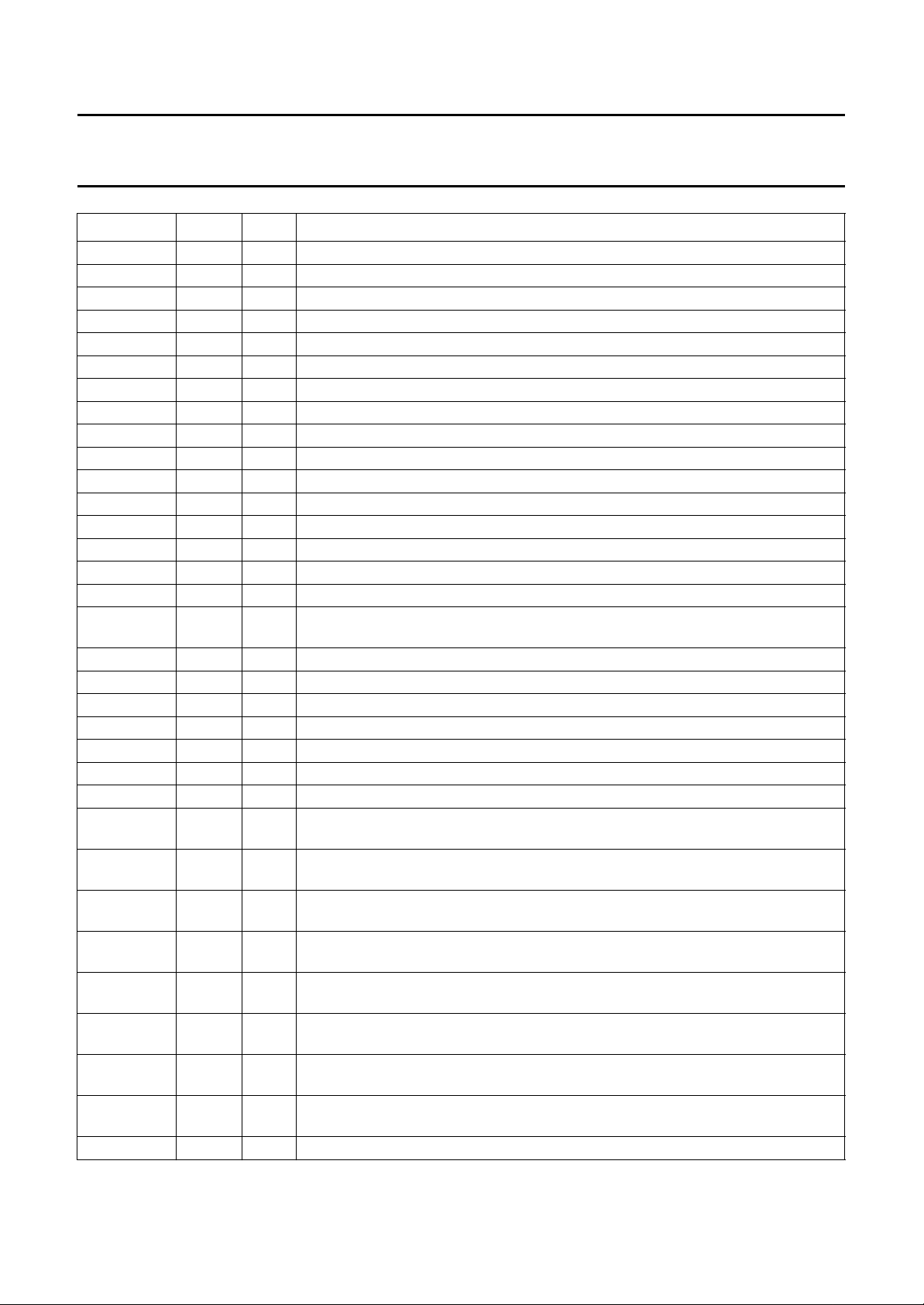
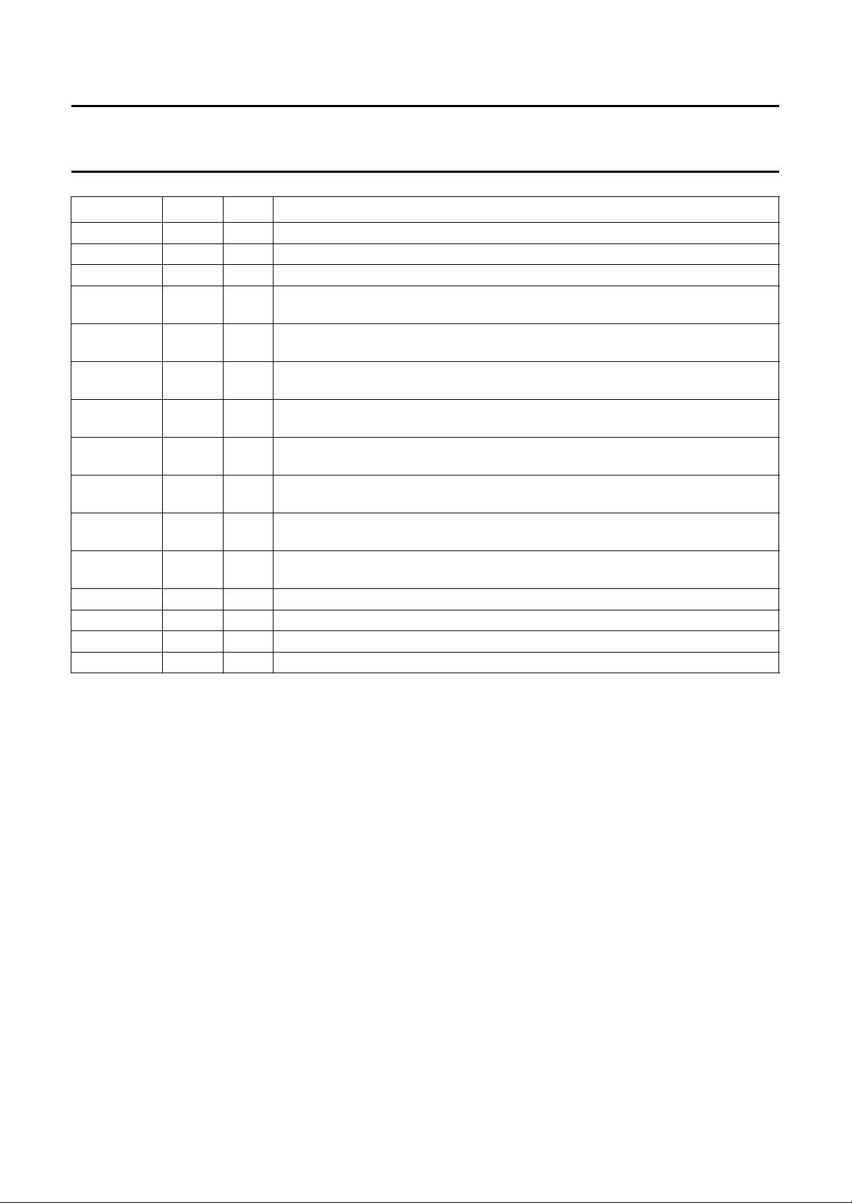
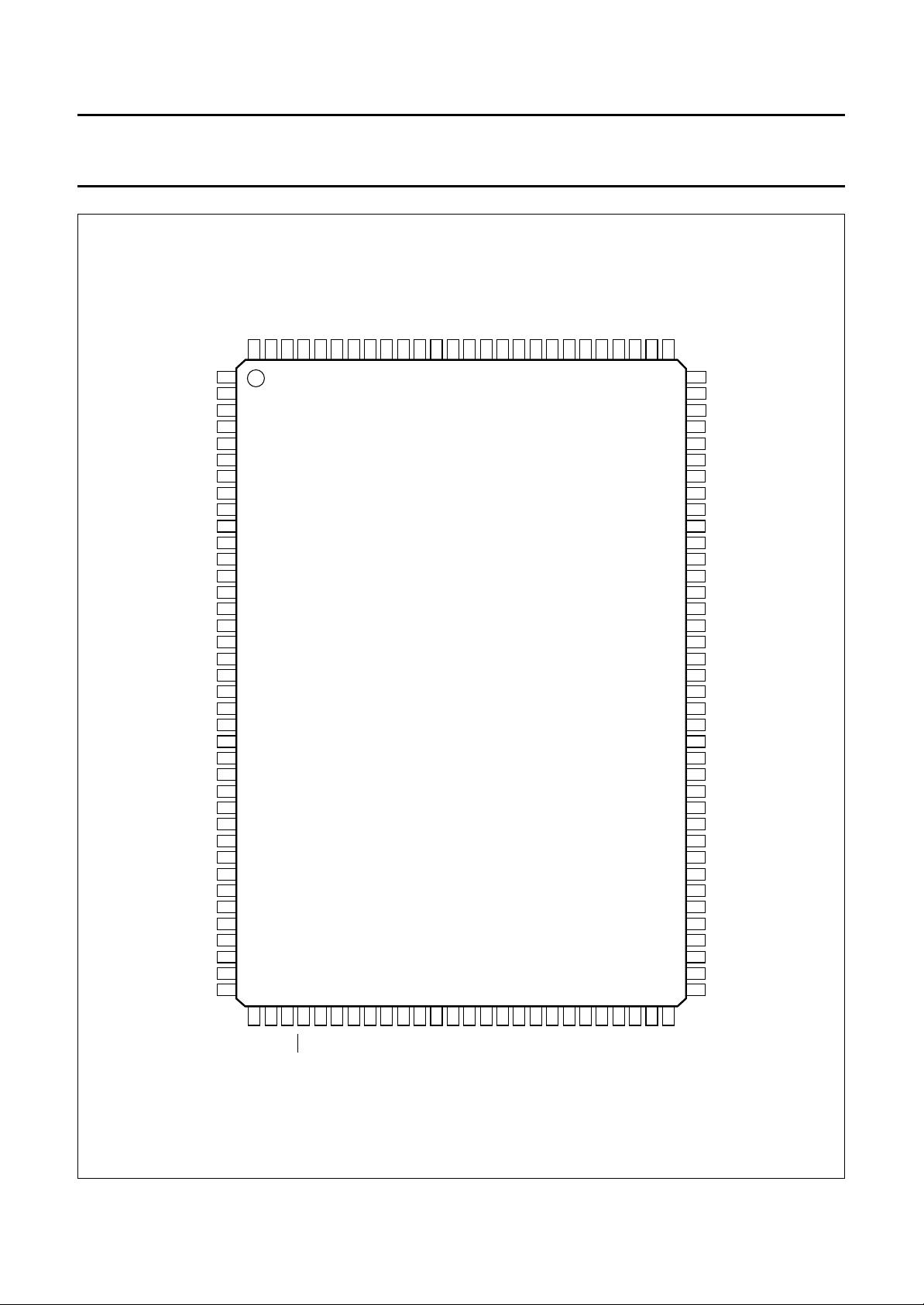
5 PINNING (SAA7140A)
SYMBOL PIN I/O DESCRIPTION
LLCIN 1 I line-locked system clock input; expansion port
V
DDD(bord)1
V
SSD(bord)1
V
DDD(bord)2
LLC 5 I line-locked system clock input, maximum 32 MHz (2 × pixel rate); DMSD port
CREF 6 I clock qualifier input (HIGH indicates valid input data YUV on DMSD port)
HREF 7 I horizontal reference input signal; DMSD port
VS 8 I vertical sync input signal; DMSD port
V
DDD(core)1
V
SSD(bord)2
YIN0 11 I luminance input data (bit 0); DMSD port
YIN1 12 I luminance input data (bit 1); DMSD port
YIN2 13 I luminance input data (bit 2); DMSD port
YIN3 14 I luminance input data (bit 3); DMSD port
YIN4 15 I luminance input data (bit 4); DMSD port
YIN5 16 I luminance input data (bit 5); DMSD port
YIN6 17 I luminance input data (bit 6); DMSD port
YIN7 18 I luminance input data (bit 7); DMSD port
V
DDD(bord)3
V
SSD(core)1
UVIN0 21 I time-multiplexed colour-difference input data (bit 0); DMSD port
UVIN1 22 I time-multiplexed colour-difference input data (bit 1); DMSD port
UVIN2 23 I time-multiplexed colour-difference input data (bit 2); DMSD port
UVIN3 24 I time-multiplexed colour-difference input data (bit 3); DMSD port
UVIN4 25 I time-multiplexed colour-difference input data (bit 4); DMSD port
UVIN5 26 I time-multiplexed colour-difference input data (bit 5); DMSD port
UVIN6 27 I time-multiplexed colour-difference input data (bit 6); DMSD port
UVIN7 28 I time-multiplexed colour-difference input data (bit 7); DMSD port
V
DDD(bord)4
V
SSD(bord)3
SDA 31 I/O serial data input/output (I
SCL 32 I serial clock input (I
IICSA 33 I set address input (I
V
DDD(bord)5
V
SSD(bord)4
V
DDD(bord)6
V
SSD(bord)5
PORT3 38 I/O general purpose port 3 input/output (set via I
PORT2 39 I/O general purpose port 2 input/output (set via I
PORT1 40 I/O general purpose port 1 input/output (set via I
2 − digital border supply voltage 1 (+5 V)
3 − digital border ground 1 (0 V)
4 − digital border supply voltage 2 (+5 V)
9 − digital core supply voltage 1 (+3.3 V)
10 − digital border ground 2 (0 V)
19 − digital border supply voltage 3 (+5 V)
20 − digital core ground 1 (0 V)
29 − digital border supply voltage 4 (+5 V)
30 − digital border ground 3 (0 V)
2
C-bus)
2
C-bus)
2
C-bus)
34 − digital border supply voltage 5 (+5 V)
35 − digital border ground 4 (0 V)
36 − digital border supply voltage 6 (+5 V)
37 − digital border ground 5 (0 V)
2
C-bus)
2
C-bus)
2
C-bus)
1996 Sep 04 6
Page 7
Philips Semiconductors Objective specification
High Performance Scaler (HPS) SAA7140A; SAA7140B
SYMBOL PIN I/O DESCRIPTION
PORT0 41 I/O general purpose port 0 input/output (set via I2C-bus)
RES 42 I reset input (active LOW for at least 30 clock cycles)
AP 43 I connected to ground (action pin for testing)
SP 44 I connected to ground (shift pin for testing)
FLDV 45 O field identification output signal; VRAM port
VSYV 46 O vertical sync output signal; VRAM port
HGTV 47 O horizontal reference output signal; VRAM port
PXQV 48 O pixel qualifier output signal to mark active pixels of a qualified line; VRAM port
BTST 49 I connected to ground; BTST = HIGH sets all outputs to high-impedance state
(testing)
VOEN 50 I enable input signal for VRAM port
V
DDD(core)2
VMUX 52 I VRAM output multiplexing, control input for the 32 to 16-bit multiplexer
V
SSD(core)2
HFL 54 O FIFO half-full flag output signal
INCADR 55 O line increment/vertical reset control output
VCLK 56 I/O clock input/output signal for VRAM port
VRO31 57 O 32-bit digital VRAM port output (bit 31)
VRO30 58 O 32-bit digital VRAM port output (bit 30)
VRO29 59 O 32-bit digital VRAM port output (bit 29)
VRO28 60 O 32-bit digital VRAM port output (bit 28)
VRO27 61 O 32-bit digital VRAM port output (bit 27)
VRO26 62 O 32-bit digital VRAM port output (bit 26)
VRO25 63 O 32-bit digital VRAM port output (bit 25)
VRO24 64 O 32-bit digital VRAM port output (bit 24)
VRO23 65 O 32-bit digital VRAM port output (bit 23)
V
DDD(bord)7
V
SSD(bord)6
V
DDD(bord)8
V
SSD(bord)7
VRO22 70 O 32-bit VRAM port output (bit 22)
VRO21 71 O 32-bit VRAM port output (bit 21)
VRO20 72 O 32-bit VRAM port output (bit 20)
VRO19 73 O 32-bit VRAM port output (bit 19)
VRO18 74 O 32-bit VRAM port output (bit 18)
VRO17 75 O 32-bit VRAM port output (bit 17)
VRO16 76 O 32-bit VRAM port output (bit 16)
VRO15 77 O 32-bit VRAM port output (bit 15)
VRO14 78 O 32-bit VRAM port output (bit 14)
VRO13 79 O 32-bit VRAM port output (bit 13)
VRO12 80 O 32-bit VRAM port output (bit 12)
51 − digital core supply voltage 2 (+3.3 V)
53 − digital core ground 2 (0 V)
66 − digital border supply voltage 7 (+5 V)
67 − digital border ground 6 (0 V)
68 − digital border supply voltage 8 (+5 V)
69 − digital border ground 7 (0 V)
1996 Sep 04 7
Page 8
Philips Semiconductors Objective specification
High Performance Scaler (HPS) SAA7140A; SAA7140B
SYMBOL PIN I/O DESCRIPTION
VRO11 81 O 32-bit VRAM port output (bit 11)
V
SSD(bord)8
V
DDD(bord)9
V
SSD(core)3
V
DDD(core)3
VRO10 86 O 32-bit VRAM port output (bit 10)
VRO9 87 O 32-bit VRAM port output (bit 9)
VRO8 88 O 32-bit VRAM port output (bit 8)
VRO7 89 O 32-bit VRAM port output (bit 7)
VRO6 90 O 32-bit VRAM port output (bit 6)
VRO5 91 O 32-bit VRAM port output (bit 5)
VRO4 92 O 32-bit VRAM port output (bit 4)
VRO3 93 O 32-bit VRAM port output (bit 3)
VRO2 94 O 32-bit VRAM port output (bit 2)
VRO1 95 O 32-bit VRAM port output (bit 1)
VRO0 96 O 32-bit VRAM port output (bit 0)
FDIO 97 I/O field identification output signal; 7196 DIR input signal expansion port, I
V
DDD(bord)10
V
SSD(bord)9
V
DDD(bord)11
V
SSD(bord)10
VIO 102 I/O vertical sync input/output signal; expansion port
HIO 103 I/O horizontal sync input/output signal; expansion port
PXQIO 104 I/O pixel qualifier input/output signal to mark valid pixels; expansion port
VIDH7 105 I/O bidirectional expansion port, high byte (bit 7) in 16-bit mode luminance
VIDH6 106 I/O bidirectional expansion port, high byte (bit 6) in 16-bit mode luminance
VIDH5 107 I/O bidirectional expansion port, high byte (bit 5) in 16-bit mode luminance
VIDH4 108 I/O bidirectional expansion port, high byte (bit 4) in 16-bit mode luminance
VIDH3 109 I/O bidirectional expansion port, high byte (bit 3) in 16-bit mode luminance
VIDH2 110 I/O bidirectional expansion port, high byte (bit 2) in 16-bit mode luminance
VIDH1 111 I/O bidirectional expansion port, high byte (bit 1) in 16-bit mode luminance
VIDH0 112 I/O bidirectional expansion port, high byte (bit 0) in 16-bit mode luminance
V
DDD(bord)12
82 − digital border ground 8 (0 V)
83 − digital border supply voltage 9 (+5 V)
84 − digital core ground 3 (0 V)
85 − digital core supply voltage 3 (+3.3 V)
controlled
98 − digital border supply voltage 10 (+5 V)
99 − digital border ground 9 (0 V)
100 − digital border supply voltage 11 (+5 V)
101 − digital border ground 10 (0 V)
component Y
component Y
component Y
component Y
component Y
component Y
component Y
component Y
113 − digital border supply voltage 12 (+5 V)
2
C-bus
1996 Sep 04 8
Page 9
Philips Semiconductors Objective specification
High Performance Scaler (HPS) SAA7140A; SAA7140B
SYMBOL PIN I/O DESCRIPTION
V
SSD(bord)11
V
DDD(core)4
V
SSD(core)4
VIDL7 117 I/O bidirectional expansion port, low byte (bit 7) in 16-bit mode time-multiplexed
VIDL6 118 I/O bidirectional expansion port, low byte (bit 6) in 16-bit mode time-multiplexed
VIDL5 119 I/O bidirectional expansion port, low byte (bit 5) in 16-bit mode time-multiplexed
VIDL4 120 I/O bidirectional expansion port, low byte (bit 4) in 16-bit mode time-multiplexed
VIDL3 121 I/O bidirectional expansion port, low byte (bit 3) in 16-bit mode time-multiplexed
VIDL2 122 I/O bidirectional expansion port, low byte (bit 2) in 16-bit mode time-multiplexed
VIDL1 123 I/O bidirectional expansion port, low byte (bit 1) in 16-bit mode time-multiplexed
VIDL0 124 I/O bidirectional expansion port, low byte (bit 0) in 16-bit mode time-multiplexed
PXQIN 125 I pixel qualifier input signal to mark valid pixels; expansion port
HIN 126 I horizontal sync input signal; expansion port
VIN 127 I vertical sync input signal; expansion port
LLCIO 128 I/O line-locked system clock input/output; expansion port
114 − digital border ground 11 (0 V)
115 − digital core supply voltage 4 (+3.3 V)
116 − digital core ground 4 (0 V)
colour-difference components U and V
colour-difference components U and V
colour-difference components U and V
colour-difference components U and V
colour-difference components U and V
colour-difference components U and V
colour-difference components U and V
colour-difference components U and V
1996 Sep 04 9
Page 10
Philips Semiconductors Objective specification
High Performance Scaler (HPS) SAA7140A; SAA7140B
handbook, full pagewidth
SSD(core)4
DDD(core)4
SSD(bord)11
V
115
DDD(bord)12
V
V
114
113
VIDH0
VIDH1
112
111
VIDH2
110
VIDH3
VIDH4
109
108
VIDH5
107
VIDH6
VIDH7
106
105
PXQIO
HIO
104
103
102
101
100
99
98
97
96
95
94
93
92
91
90
89
88
87
86
85
84
83
82
81
80
79
78
77
76
75
74
73
72
71
70
69
68
67
66
65
VIO
V
SSD(bord)10
V
DDD(bord)11
V
SSD(bord)9
V
DDD(bord)10
FDIO
VRO0
VRO1
VRO2
VRO3
VRO4
VRO5
VRO5
VRO7
VRO8
VRO9
VRO10
V
DDD(core)3
V
SSD(core)3
V
DDD(bord)9
V
SSD(bord)8
VRO11
VRO12
VRO13
VRO14
VRO15
VRO16
VRO17
VRO18
VRO19
VRO20
VRO21
VRO22
V
SSD(bord)7
V
DDD(bord)8
V
SSD(bord)6
V
DDD(bord)7
VRO23
V
DDD(bord)1
V
SSD(bord)1
V
DDD(bord)2
V
DDD(core)1
V
SSD(bord)2
V
DDD(bord)3
V
SSD(core)1
V
DDD(bord)4
V
SSD(bord)3
V
DDD(bord)5
V
SSD(bord)4
V
DDD(bord)6
V
SSD(bord)5
PORT3
LLCIN
LCC
CREF
HREF
VS
YIN0
YIN1
YIN2
YIN3
YIN4
YIN5
YIN6
YIN7
UVIN0
UVIN1
UVIN2
UVIN3
UVIN4
UVIN5
UVIN6
UVIN7
SDA
SCL
IICSA
VIN
LLCIO
HIN
PXQIN
VIDL0
VIDL1
VIDL2
VIDL3
VIDL4
VIDL5
VIDL6
VIDL7
V
127
128
126
125
124
123
122
121
120
119
118
117
116
1
2
3
4
5
6
7
8
9
10
11
12
13
14
15
16
17
18
19
20
21
22
23
24
25
26
27
28
29
30
31
32
33
34
35
36
37
38
SAA7140A
40394142434445464748495051525354555657585960616263
AP
SP
PORT1
PORT2
RES
PORT0
FLDV
VSYV
HGTV
PXQV
BTST
VOEN
DDD(core)2
V
Fig.3 Pin configuration (SAA7140A).
1996 Sep 04 10
VMUX
SSD(core)2
V
HFL
VCLK
INCADR
VRO31
VRO30
VRO29
VRO28
VRO27
VRO26
64
VRO25
VRO24
MHA362
Page 11

Philips Semiconductors Objective specification
High Performance Scaler (HPS) SAA7140A; SAA7140B
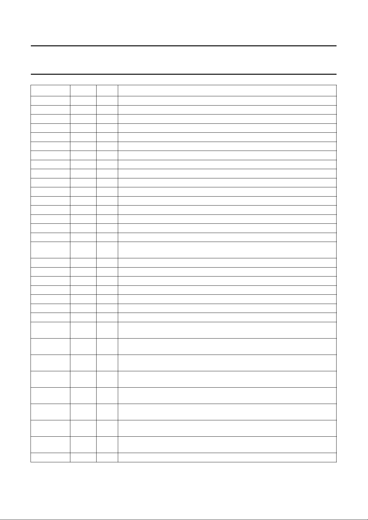
6 PINNING (SAA7140B)
SYMBOL PIN I/O DESCRIPTION
LLCIN 1 I line-locked system clock input; expansion port
V
DDD1
V
SSD1
V
DDD2
LLC 5 I line-locked system clock input, maximum 32 MHz (2 × pixel rate); DMSD port
CREF 6 I clock qualifier input (HIGH indicates valid input data YUV on DMSD port)
HREF 7 I horizontal reference input signal; DMSD port
VS 8 I vertical sync input signal; DMSD port
V
DDD3
V
SSD2
YIN0 11 I luminance input data (bit 0); DMSD port
YIN1 12 I luminance input data (bit 1); DMSD port
YIN2 13 I luminance input data (bit 2); DMSD port
YIN3 14 I luminance input data (bit 3); DMSD port
YIN4 15 I luminance input data (bit 4); DMSD port
YIN5 16 I luminance input data (bit 5); DMSD port
YIN6 17 I luminance input data (bit 6); DMSD port
YIN7 18 I luminance input data (bit 7); DMSD port
V
DDD4
V
SSD3
UVIN0 21 I time-multiplexed colour-difference input data (bit 0); DMSD port
UVIN1 22 I time-multiplexed colour-difference input data (bit 1); DMSD port
UVIN2 23 I time-multiplexed colour-difference input data (bit 2); DMSD port
UVIN3 24 I time-multiplexed colour-difference input data (bit 3); DMSD port
UVIN4 25 I time-multiplexed colour-difference input data (bit 4); DMSD port
UVIN5 26 I time-multiplexed colour-difference input data (bit 5); DMSD port
UVIN6 27 I time-multiplexed colour-difference input data (bit 6); DMSD port
UVIN7 28 I time-multiplexed colour-difference input data (bit 7); DMSD port
V
DDD5
V
SSD4
SDA 31 I/O serial data input/output (I
SCL 32 I serial clock input (I
IICSA 33 I set address input (I
V
DDD6
V
SSD5
V
DDD7
V
SSD6
PORT3 38 I/O general purpose port 3 input/output (set via I
PORT2 39 I/O general purpose port 2 input/output (set via I
PORT1 40 I/O general purpose port 1 input/output (set via I
2 − digital supply voltage 1 (+3.3 V)
3 − digital ground 1 (0 V)
4 − digital supply voltage 2 (+3.3 V)
9 − digital supply voltage 3 (+3.3 V)
10 − digital ground 2 (0 V)
19 − digital supply voltage 4 (+3.3 V)
20 − digital ground 3 (0 V)
29 − digital supply voltage 5 (+3.3 V)
30 − digital ground 4 (0 V)
2
C-bus)
2
C-bus)
2
C-bus)
34 − digital supply voltage 6 (+3.3 V)
35 − digital ground 5 (0 V)
36 − digital supply voltage 7 (+3.3 V)
37 − digital ground 6 (0 V)
2
C-bus)
2
C-bus)
2
C-bus)
1996 Sep 04 11
Page 12

Philips Semiconductors Objective specification
High Performance Scaler (HPS) SAA7140A; SAA7140B
SYMBOL PIN I/O DESCRIPTION
PORT0 41 I/O general purpose port 0 input/output (set via I2C-bus)
RES 42 I reset input (active LOW for at least 30 clock cycles)
AP 43 I connected to ground (action pin for testing)
SP 44 I connected to ground (shift pin for testing)
FLDV 45 O field identification output signal; VRAM port
VSYV 46 O vertical sync output signal; VRAM port
HGTV 47 O horizontal reference output signal; VRAM port
PXQV 48 O pixel qualifier output signal to mark active pixels of a qualified line; VRAM port
BTST 49 I connected to ground; BTST = HIGH sets all outputs to high-impedance state
(testing)
VOEN 50 I enable input signal for VRAM port
V
DDD8
VMUX 52 I VRAM output multiplexing, control input for the 32 to 16-bit multiplexer
V
SSD7
HFL 54 O FIFO half-full flag output signal
INCADR 55 O line increment/vertical reset control output
VCLK 56 I/O clock input/output signal for VRAM port
VRO31 57 O 32-bit digital VRAM port output (bit 31)
VRO30 58 O 32-bit digital VRAM port output (bit 30)
VRO29 59 O 32-bit digital VRAM port output (bit 29)
VRO28 60 O 32-bit digital VRAM port output (bit 28)
VRO27 61 O 32-bit digital VRAM port output (bit 27)
VRO26 62 O 32-bit digital VRAM port output (bit 26)
VRO25 63 O 32-bit digital VRAM port output (bit 25)
VRO24 64 O 32-bit digital VRAM port output (bit 24)
VRO23 65 O 32-bit digital VRAM port output (bit 23)
V
DDD9
V
SSD8
V
DDD10
V
SSD9
VRO22 70 O 32-bit VRAM port output (bit 22)
VRO21 71 O 32-bit VRAM port output (bit 21)
VRO20 72 O 32-bit VRAM port output (bit 20)
VRO19 73 O 32-bit VRAM port output (bit 19)
VRO18 74 O 32-bit VRAM port output (bit 18)
VRO17 75 O 32-bit VRAM port output (bit 17)
VRO16 76 O 32-bit VRAM port output (bit 16)
VRO15 77 O 32-bit VRAM port output (bit 15)
VRO14 78 O 32-bit VRAM port output (bit 14)
VRO13 79 O 32-bit VRAM port output (bit 13)
VRO12 80 O 32-bit VRAM port output (bit 12)
51 − digital supply voltage 8 (+3.3 V)
53 − digital ground 7 (0 V)
66 − digital supply voltage 9 (+3.3 V)
67 − digital ground 8 (0 V)
68 − digital supply voltage 10 (+3.3 V)
69 − digital ground 9 (0 V)
1996 Sep 04 12
Page 13
Philips Semiconductors Objective specification
High Performance Scaler (HPS) SAA7140A; SAA7140B
SYMBOL PIN I/O DESCRIPTION
VRO11 81 O 32-bit VRAM port output (bit 11)
V
SSD10
V
DDD11
V
SSD11
V
DDD12
VRO10 86 O 32-bit VRAM port output (bit 10)
VRO9 87 O 32-bit VRAM port output (bit 9)
VRO8 88 O 32-bit VRAM port output (bit 8)
VRO7 89 O 32-bit VRAM port output (bit 7)
VRO6 90 O 32-bit VRAM port output (bit 6)
VRO5 91 O 32-bit VRAM port output (bit 5)
VRO4 92 O 32-bit VRAM port output (bit 4)
VRO3 93 O 32-bit VRAM port output (bit 3)
VRO2 94 O 32-bit VRAM port output (bit 2)
VRO1 95 O 32-bit VRAM port output (bit 1)
VRO0 96 O 32-bit VRAM port output (bit 0)
FDIO 97 I/O field identification output signal; 7196 DIR input signal expansion port, I
V
DDD13
V
SSD12
V
DDD14
V
SSD13
VIO 102 I/O vertical sync input/output signal; expansion port
HIO 103 I/O horizontal sync input/output signal; expansion port
PXQIO 104 I/O pixel qualifier input/output signal to mark valid pixels; expansion port
VIDH7 105 I/O bidirectional expansion port, high byte (bit 7) in 16-bit mode luminance
VIDH6 106 I/O bidirectional expansion port, high byte (bit 6) in 16-bit mode luminance
VIDH5 107 I/O bidirectional expansion port, high byte (bit 5) in 16-bit mode luminance
VIDH4 108 I/O bidirectional expansion port, high byte (bit 4) in 16-bit mode luminance
VIDH3 109 I/O bidirectional expansion port, high byte (bit 3) in 16-bit mode luminance
VIDH2 110 I/O bidirectional expansion port, high byte (bit 2) in 16-bit mode luminance
VIDH1 111 I/O bidirectional expansion port, high byte (bit 1) in 16-bit mode luminance
VIDH0 112 I/O bidirectional expansion port, high byte (bit 0) in 16-bit mode luminance
V
DDD15
82 − digital ground 10 (0 V)
83 − digital supply voltage 11 (+3.3 V)
84 − digital ground 11 (0 V)
85 − digital supply voltage 12 (+3.3 V)
controlled
98 − digital supply voltage 13 (+3.3 V)
99 − digital ground 12 (0 V)
100 − digital supply voltage 14 (+3.3 V)
101 − digital ground 13 (0 V)
component Y
component Y
component Y
component Y
component Y
component Y
component Y
component Y
113 − digital supply voltage 15 (+3.3 V)
2
C-bus
1996 Sep 04 13
Page 14
Philips Semiconductors Objective specification
High Performance Scaler (HPS) SAA7140A; SAA7140B
SYMBOL PIN I/O DESCRIPTION
V
SSD14
V
DDD16
V
SSD15
VIDL7 117 I/O bidirectional expansion port, low byte (bit 7) in 16-bit mode time-multiplexed
VIDL6 118 I/O bidirectional expansion port, low byte (bit 6) in 16-bit mode time-multiplexed
VIDL5 119 I/O bidirectional expansion port, low byte (bit 5) in 16-bit mode time-multiplexed
VIDL4 120 I/O bidirectional expansion port, low byte (bit 4) in 16-bit mode time-multiplexed
VIDL3 121 I/O bidirectional expansion port, low byte (bit 3) in 16-bit mode time-multiplexed
VIDL2 122 I/O bidirectional expansion port, low byte (bit 2) in 16-bit mode time-multiplexed
VIDL1 123 I/O bidirectional expansion port, low byte (bit 1) in 16-bit mode time-multiplexed
VIDL0 124 I/O bidirectional expansion port, low byte (bit 0) in 16-bit mode time-multiplexed
PXQIN 125 I pixel qualifier input signal to mark valid pixels; expansion port
HIN 126 I horizontal sync input signal; expansion port
VIN 127 I vertical sync input signal; expansion port
LLCIO 128 I/O line-locked system clock input/output; expansion port
114 − digital ground 14 (0 V)
115 − digital supply voltage 16 (+3.3 V)
116 − digital ground 15 (0 V)
colour-difference components U and V
colour-difference components U and V
colour-difference components U and V
colour-difference components U and V
colour-difference components U and V
colour-difference components U and V
colour-difference components U and V
colour-difference components U and V
1996 Sep 04 14
Page 15
Philips Semiconductors Objective specification
High Performance Scaler (HPS) SAA7140A; SAA7140B
handbook, full pagewidth
SSD15VDDD16VSSD14VDDD15
VIDL6
VIDL7
V
118
117
116
SAA7140B
115
114
113
VIDH0
VIDH1
112
111
VIDH2
VIDH3
110
109
VIDH4
108
VIDH5
VIDH6
107
106
VIDH7
PXQIO
105
104
HIO
103
102
101
100
99
98
97
96
95
94
93
92
91
90
89
88
87
86
85
84
83
82
81
80
79
78
77
76
75
74
73
72
71
70
69
68
67
66
65
VIO
V
SSD13
V
DDD14
V
SSD12
V
DDD13
FDIO
VRO0
VRO1
VRO2
VRO3
VRO4
VRO5
VRO6
VRO7
VRO8
VRO9
VRO10
V
DDD12
V
SSD11
V
DDD11
V
SSD10
VRO11
VRO12
VRO13
VRO14
VRO15
VRO16
VRO17
VRO18
VRO19
VRO20
VRO21
VRO22
V
SSD9
V
DDD10
V
SSD8
V
DDD9
VRO23
LLCIN
V
DDD1
V
SSD1
V
DDD2
LLC
CREF
HREF
VS
V
DDD3
V
SSD2
YIN0
YIN1
YIN2
YIN3
YIN4
YIN5
YIN6
YIN7
V
DDD4
V
SSD3
UVIN0
UVIN1
UVIN2
UVIN3
UVIN4
UVIN5
UVIN6
UVIN7
V
DDD5
V
SSD4
SDA
SCL
IICSA
V
DDD6
V
SSD5
V
DDD7
V
SSD6
PORT3
VIN
LLCIO
HIN
PXQIN
VIDL0
VIDL1
VIDL2
VIDL3
VIDL4
VIDL5
127
128
126
125
124
123
122
121
120
119
1
2
3
4
5
6
7
8
9
10
11
12
13
14
15
16
17
18
19
20
21
22
23
24
25
26
27
28
29
30
31
32
33
34
35
36
37
38
40394142434445464748495051525354555657585960616263
AP
SP
PORT1
PORT2
RES
PORT0
FLDV
VSYV
HGTV
PXQV
BTST
VOEN
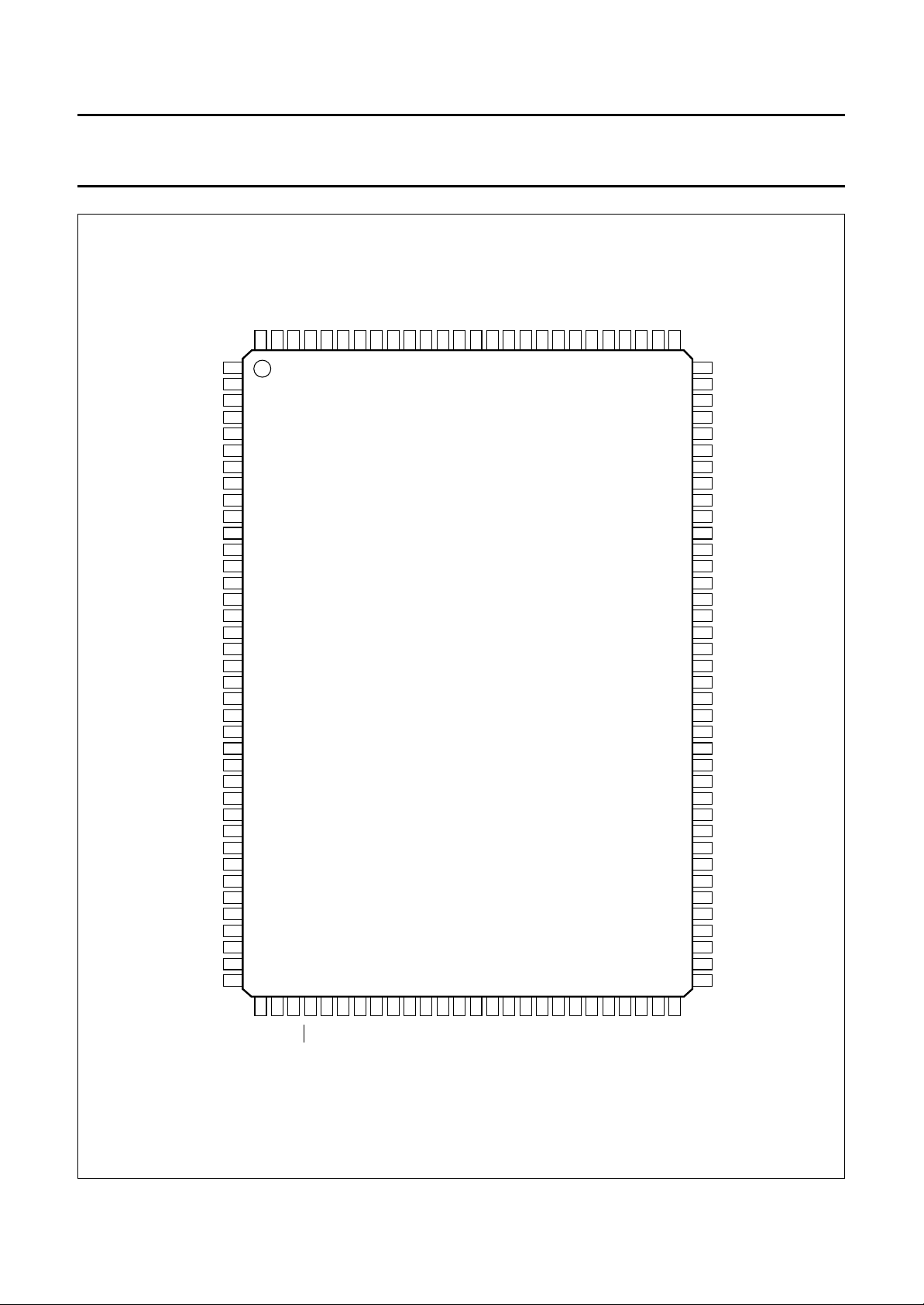
Fig.4 Pin configuration (SAA7140B).
1996 Sep 04 15
DDD8
V
VMUX
V
SSD7
HFL
VCLK
INCADR
VRO31
VRO30
VRO29
VRO28
VRO27
VRO26
64
VRO25
VRO24
MHA359
Page 16

Philips Semiconductors Objective specification
High Performance Scaler (HPS) SAA7140A; SAA7140B
7 FUNCTIONAL DESCRIPTION
The SAA7140A and SAA7140B accepts YUV data in a
16-bit wide parallel format at the DMSD port and accepts
YUV input in a 16-bit wide parallel format and in an 8-bit
byte-multiplexed Cb-Y-Cr-Y- format (CCIR-656 or
D1 oriented) at the expansion port.
Depending on the selected port modes, the incoming data
is formatted to the internal data representation, where
reference signals or codes are detected in the Data
Formatter/Reformatter (DFR). The horizontal and vertical
timing reference can be defined under I
Based on that timing reference, the active processing
window is defined in a versatile way via the programming.
Two programming sets can be loaded simultaneously, and
become valid for processing in a field alternating way.
Before being processed in the central scaling unit, the
incoming data passes through the BCS control unit where
monitor control functions, for adjusting brightness, contrast
(luminance) and saturation (chrominance) are
implemented.
The scaling is performed in three steps:
1. Horizontal prescaling (bandwidth limitation for
anti-aliasing, via FIR prefiltering and subsampling)
2. Vertical scaling (generating phase interpolated or
vertically low-passed lines)
3. Horizontal variable phase scaling (phase-correct
scaling to the new geometric relationships).
The scaled output data is fed back to the DFR unit and
may be used as output signals from the bidirectional
expansion port (if the mode is selected). They are
converted in parallel from the YUV to the RGB domain in a
digital matrix. Anti-gamma correction of gamma-corrected
input signals can be performed in the RGB data path.
The output formatter then formats the scaled data to one
of the various output formats (e.g. monochrome, 16-bit
YUV or 32-bit RGB (5, 5, 5).
To ease frame buffer applications, the data can be
transferred in a synchronous way (transparent mode),
using separate reference and qualifier signals and a
continuous output clock (VCLK). The data can also be
transferred in an asynchronous way (burst mode) using
the HFL and INCADR flags and a discontinuous input
clock burst on VCLK.
2
C-bus control.
In a typical application, the 16-bit wide YUV input receives
clock, sync and data from a video decoder (SAA71xx) via
the DMSD port. An MPEG compression/decompression
circuit can be connected at the expansion port to receive
the decoder data, scaled or unscaled, or to deliver data to
the scaling processor. The scaling operation of the
SAA7140A and SAA7140B can be performed on the data
from a video decoder, or on the data from the
MPEG-codec at the expansion port input. The source
selection can be static or toggled on a field-by-field basis.
For example, during the odd field the video decoder signal
is scaled in accordance with the ‘odd’ parameter set for
display in a window. The compression codec receives
unscaled data. During the even field the decompressed
data from the MPEG decoder gets sized for a second
display window in accordance with the ‘even’ parameter
set. The resulting output from the scaling operation is
delivered via the 32-bit wide output (VRAM port) and to the
expansion port output (optional).
7.1 Data format/reformatter and reference signal generation
The video data can be formatted/reformatted in
accordance with the selected expansion port mode, from
16-bit (DMSD port) to serial 8-bit (expansion port output),
from serial 8-bit (expansion port input) to internal parallel
16-bit format and from 24-bit (scaler output) to 16-bit/8-bit
respectively (expansion port output). The definition of the
timing references for the acquisition and field detection
(polarity and edge selection) are based on the selected
reference signal source. The field detector regenerates the
field information from the selected incoming reference
signals (see Fig.5).
The field sequence flag (FLD), detects the state of the
H-sync signal at the reference edge of the V-sync signal.
The detection is controlled by I
INVOE. The detection output can be seen on pins FLDV
and FDIO (if FLDC = 0). Bits IREGS and SREGS control
the mapping of the detected sequence to the I2C-bus
register sets A and B (I2C-bus subaddress 02 to 1F and
22 to 3F).
2
C-bus bits REVFLD and
1996 Sep 04 16
Page 17

Philips Semiconductors Objective specification
High Performance Scaler (HPS) SAA7140A; SAA7140B
handbook, full pagewidth
(corresponding
REGISTER 00
INVOE
active
horizontal
state
SOURCE SELECT
FIELD DETECTION
H
F
to VF)
FIELD DETECTION
REVFLD
active
vertical
edge
V
F
(1)
detected field
V source select
H/V expansion port
H/V DMSD
REGISTER 00
REGISTER SET
MAPPING FIELD
REGISTER A REGISTER B
MULTIPLEXER
active
horizontal
edge
n × τ
m × τ
active
vertical
edge
SOURCE SELECT
SCALER
HV
AQUISITION CONTROL
SCALER
FIDO
(expansion port)
FLDV
(VRAM)
(or frame sync)
select
H/V
source
select
FLD IIC
MHA118
FLD detection modes (I2C-bus bits FICO1 and FICO0);
(1) In the normal mode: the FLD signal is detected from the incoming
H andV signals.
In the improved mode: the FLD signal is resynchronized only after
the H andV sequence runs stable for a certain period of time.
In the force toggle mode: the FLD signal toggles with every event on
the V signal (His independent).
Fig.5 Field detection/register set mapping.
7.1.1 DATA FORMATS AND REFERENCE SIGNALS OF THE
DMSD PORT
The 16-bit YUV colour difference and luminance signals
(straight binary) are available in parallel on a 16-bit wide
data stream. The code is in accordance with CCIR-601;
black = 16, white = 235, no colour = 128, 100% colour
saturation = 16 to 240 etc. Overshoots and undershoots
are permitted and supported, i.e. processed as they are.
The 16-bit wide YUV data format from the DMSD port
(input only) is defined with Line-Locked Clock (LLC) with a
double pixel clock frequency. Every second clock cycle is
qualified with CREF, in pixel rate frequency.
Register set mapping modes (I2C-bus bits IREGS and SREGS);
The FLD_IIC signal carries the detected FLD or the inverted FLD.
The signal is fixed to 0 (Register setA forced) or forced to 1
(Register set A forced).
The internal processing of the SAA7140A and SAA7140B
relies on the presence of LLC, i.e. a clock of at least twice
the sampling rate of the input data stream. The maximum
LLC rate is 32 MHz.
The horizontal sync input (HREF) may be supplied as a
H-pulse or horizontal gate signal. The positive or negative
edge, (programmable by I
2
C-bus bit REHAW), indicates
the horizontal timing reference. The first valid pixels may
occur not exactly at the start of the line but with a certain
offset (counted in qualified pixels).
1996 Sep 04 17
Page 18

Philips Semiconductors Objective specification
High Performance Scaler (HPS) SAA7140A; SAA7140B
The vertical timing is indicated by the positive or negative
edge (programmable by I2C-bus bit REVAW) of the sync
input signal VS. The first valid line may occur not exactly
at the start of the field but with a certain offset, counted in
lines, with qualified pixels. Input signal VS defines, in
relation to HREF, the odd/even field detection
(see
SAA7191B
7.1.2 D
).
ATA FORMATS AND REFERENCE SIGNALS OF THE
EXPANSION PORT
The expansion port (input/output) supports several modes;
simultaneous (parallel) D1 input and D1 output (full
duplex) with auxiliary sync and qualifying signals, or 16-bit
wide YUV input or output (half duplex), selected via
programming with clock, qualify and sync signal.
A discontinuous data stream is supported by accepting or
generating a pixel/byte qualifying signal (PXQ), a
generalization of the CREF definition at the DMSD port
(PXQ = 1 qualified pixel, PXQ = 0 invalid data).
16-bit YUV (half duplex mode = field alternating data I/O):
16-bit YUV data stream (Y = VIDH7 to VIDH0,
UV = VIDL7 to VIDL0). For the 16-bit YUV data input
format, PXQ is inhibited from qualifying adjacent LLC clock
cycles. There must be at least one empty clock cycle
between two valid pixels.
8-bit Cb-Y-Cr-Y; CCIR 656 or D1 (full duplex mode): the
colour difference signals and the luminance signal
(straight binary) are byte-wise multiplexed onto the same
8-bit wide data stream, with sequence and timing in
accordance with CCIR 656 recommendations (according
to D1 for 60 Hz application respectively). The code is in
accordance with CCIR 601 (black = 16, white = 235, no
colour = 128, 100% colour saturation = 16 or 240, etc.
Overshoots and undershoots are permitted and
supported, i.e. processed as they are.
If the CCIR 656 output is selected, the video signal is
clipped to 01H and FEH in order to leave the codes 00H
and FFH for SAV and EAV encoding (SAV and EAV
encoding not yet supported). The clock rate for this format
is twice the pixel clock.
The horizontal sync input HIN is processed in an identical
manner to HREF at the DMSD port. If the CCIR 656 data
input format is selected, the horizontal timing reference is
decoded from the input data stream (SAV, EAV and
SHVS = 1) or taken from the selected H-reference signal
HIN, HREF or HIO (SHVS = 0). The start condition to
enable synchronization to the correct Cb-Y-Cr-Ysequence is provided by the selected horizontal reference
signal. The sequence only increments with qualified bytes.
Instead of a vertical sync signal, as described for the
DMSD port, the expansion port also supports an odd/even
signal applied to the input pin VIN or VIO (controlled by
2
I
C-bus bit FSEL). The frame and the field timing is then
indicated by a positive or negative edge of the V input.
This may occur with a certain offset at the frame and field
start, and is normally counted in lines.
If the CCIR 656 data input format is selected, the vertical
timing reference is decoded from the input data stream by
SAV and EAV (SHVS = 1) or taken from the selected V
reference signal VIN, VS or VIO (SHVS = 0). The vertical
synchronization pin can be programmed to carry either a
vertical sync signal or an odd/even signal.
The horizontal and vertical sync outputs HIO and VIO are
expansion port mode dependent and can be selected via
the I2C-bus (VD1/VD0 and HD1/HD0):
Should the DMSD port be selected as the output source,
HIO will carry a copy of HREF and VIO will carry a copy
of VS.
If the expansion port carries data from the scaler output,
then HIO is a gate signal enveloping the range of active
video along a line and VIO is a positive sync pulse with
a length of 4 lines
If HIN/VIN is selected as the output source, HIO carries
a copy of HIN and VIO carries a copy of VIN (short cut).
If the CCIR 656 data output format is selected, the
horizontal and vertical sync output signals are only
supplied at pins HIO and VIO (SAV and EAV are not
encoded as outputs).
Due to compatibility reasons to the expansion port
definition of the SAA7194/SAA7196 circuits, the
bidirectional pins HIO, VIO and PXQIO can also be
configured as input pins (see Table 3).
The definition of the pin FDIO is I2C-bus selectable.
Configured as an output pin, FDIO carries an odd/even
signal generated in the FLD detection (see Fig.5).
Configured as an input pin, FDIO controls the direction of
the expansion port (compatibility to SAA7194/SAA7196,
(see Table 3 and Chapter 8).
1996 Sep 04 18
Page 19

Philips Semiconductors Objective specification
High Performance Scaler (HPS) SAA7140A; SAA7140B
handbook, full pagewidth
LLC
CREF
PXQIN
VIDL7 to 0
VIDH7 to 0
HIN
Cb0
Cr0 Cb2 Cr2
Y0 Y1 Y2 Y3
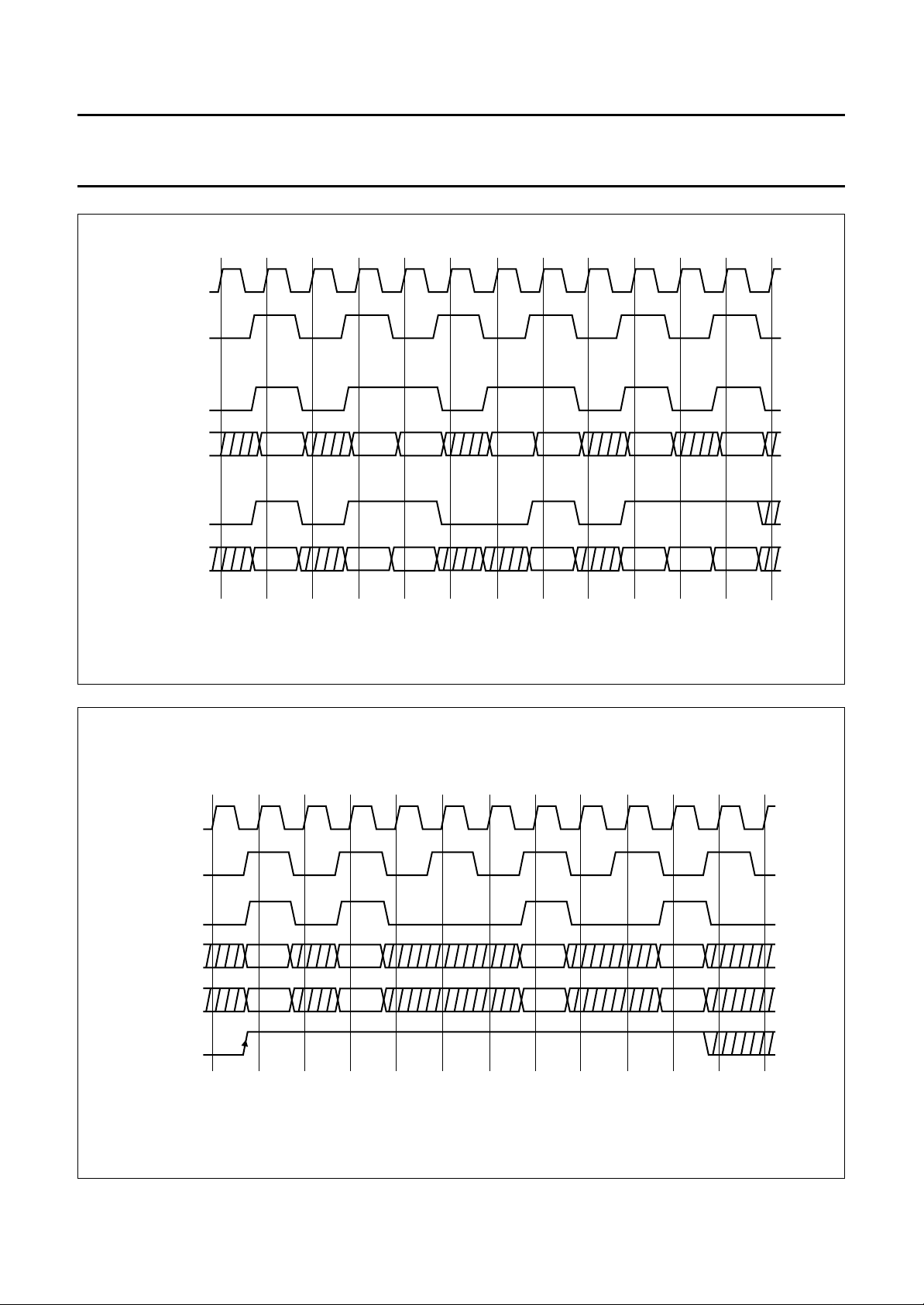
Fig.6 Timing of PXQIN for 16-bit data input from DMSD to expansion port.
MHA126
handbook, full pagewidth
LLC
CREF
PXQIN
VIDL7 to 0
HIN
Cb Y Y Y Cr Cb
Fig.7 Timing of PXQIO for serial 8-bit data input at expansion port.
1996 Sep 04 19
MHA130
Page 20
Philips Semiconductors Objective specification
High Performance Scaler (HPS) SAA7140A; SAA7140B
handbook, full pagewidth
LLC
CREF
PXQIN/PXQIO
VIDL7 to 0
PXQIN/PXQIO
VIDL7 to 0
handbook, full pagewidth
LLC
CREF
FFH 00H 00H Cb SAV
Y Cr Y FFH 00H 00H
Y Cr
Fig.8 Timing of PXQIN/PXQIO for CCIR 656 data input at expansion port.
EAV
MHA129
PXQIO
VIDL7 to 0
VIDH7 to 0
HIO
Cb0 Cr0
Y0 Y1
Fig.9 Timing of PXQIO for non-zoomed 16-bit data output at expansion port.
1996 Sep 04 20
Cb2
Y2
Cr2
Y3
MHA127
Page 21

Philips Semiconductors Objective specification
High Performance Scaler (HPS) SAA7140A; SAA7140B
handbook, full pagewidth
LLC
CREF
PXQIO
VIDL7 to 0
VIDH7 to 0
HIO
handbook, full pagewidth
LLC
CREF
Cb0 Cr0 Cb2 Cr2 Cr4 Cb4
Y0 Y1 Y2 Y3 Y5 Y6 Y4
Cb6 Cr6
Fig.10 Timing of PXQIN for zoomed 16-bit data output at expansion port.
Y7
MHA128
PXQIO
VIDL7 to 0
HIO
Cb Y Y Y Cr Cb
Fig.11 Timing of PXQIO for serial 8-bit data output at expansion port.
1996 Sep 04 21
Cr Y
MHA131
Page 22
Philips Semiconductors Objective specification
High Performance Scaler (HPS) SAA7140A; SAA7140B
7.2 Acquisition control
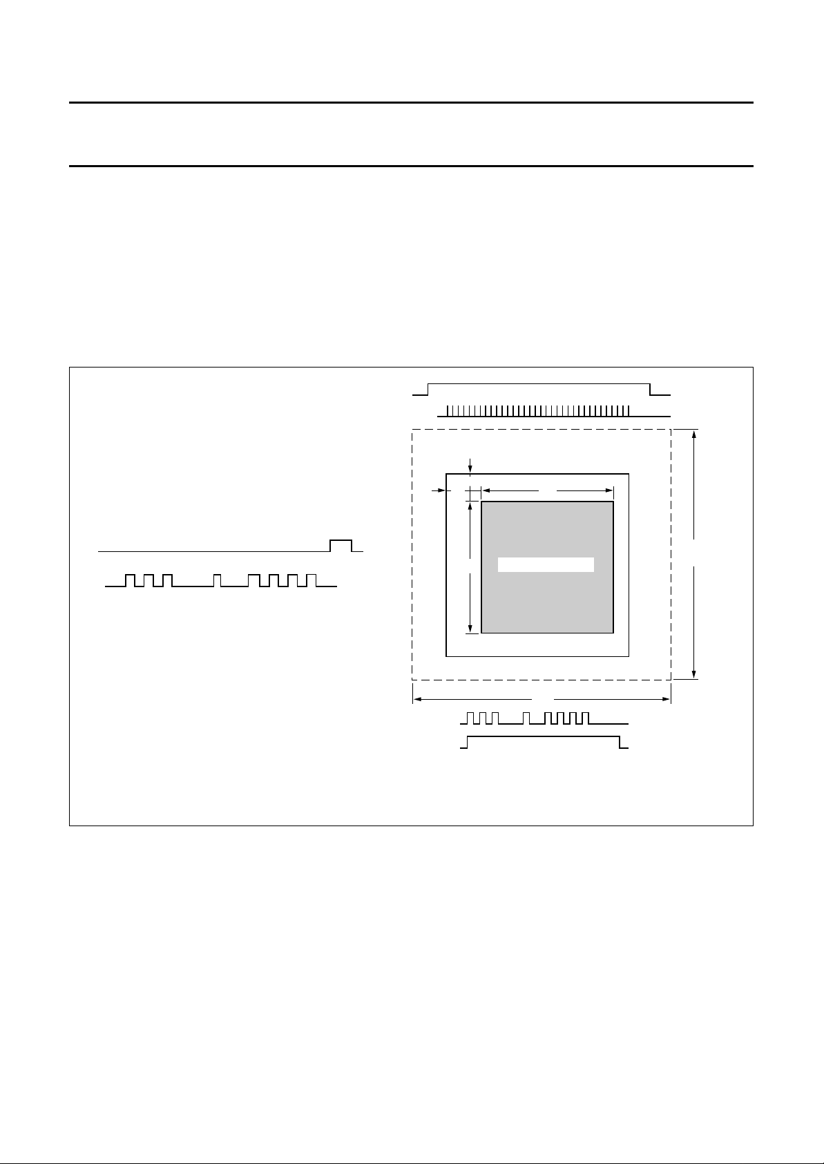
The processing window for the scaling unit is defined in the
acquisition control unit. An internal counter receives
I2C-bus controlled values for offset (bits XO10 to XO0 and
YO10 to YO0) and length (bits XS10 to XS0 and
YS10 to YS0). The counter is reset by the corresponding
sync reference input signal. The horizontal counter
increments in qualified pixels and the vertical counter
increments in qualified lines, i.e. lines containing at least
handbook, full pagewidth
VIN/VS
(1)
LQ
one qualified pixel. Depending on the selected mode, the
source for the horizontal reference may be HREF (DMSD
port) or HIN (expansion port), or for the vertical reference,
VS (DMSD port) or VIN (expansion port).
It should be noted that in order to avoid programming
dependent line and field drop effects, all values must not
exceed the number of qualified pixels per line or lines per
field.
HIN/HREF
PXQ/CREF
ACTIVE VIDEO WINDOW
yo
xo
ys
xs
SCALING WINDOW
field/
frame
output signals
(1) LQ = qualified lines i.e. lines containing at least one qualified pixel.
Fig.12 Reference signals for scaling window.
7.3 BCS control
The parameters for Brightness, Contrast and Saturation
(BSC) can be adjusted in the BSC control unit.
The luminance signal can be controlled via the I2C-bus
using bits BRIG7 to BRIG0 and CONT6 to CONT0.
For the brightness control:
00H = minimum offset
80H = nominal level
FFH = maximum offset.
1996 Sep 04 22
line
PXQV
HGTV
MHA119
For the contrast control:
00H = luminance off
40H = nominal gain of 1.01
7FH = maximum gain of 1.9999.
The chrominance signal can be controlled via the I
using bits SAT6 to SAT0.
For the saturation control:
00H = colour off
40H = nominal gain of 1.0
7FH = maximum gain of 1.9999.
2
C-bus
Page 23

Philips Semiconductors Objective specification
High Performance Scaler (HPS) SAA7140A; SAA7140B
With respect to limiting, all values are limited to minimum
(equals 0) and maximum (equals 255).
7.4 Scaling unit
Scaling to a randomly sized window is performed in three
steps:
1. Horizontal prescaling (bandwidth limitation for
anti-aliasing, via FIR prefiltering and subsampling)
2. Vertical scaling (generating phase interpolated or
vertically low-passed lines)
3. Horizontal variable phase scaling (phase-correct
scaling to the new geometric relations).
The scaling processor can obtain its clock from the DMSD
port or the expansion port. Normally the two ports are
synchronized to support program-set-swapping,
asynchronous working results in restricted operation.
The video signal source also provides the source for the
scalers qualify signal PXQ.
The scaling process generates a new pixel/clock qualifier
sequence. This results in PXQ being used at the VRAM
port in the transparent mode, and for the expansion port
output. There are restrictions in the combination of the
input sample rate and up or down-scaling mode and
scaling factor. The maximum resulting output sample rate
at the VRAM port is LLC and at the expansion port the
1
maximum pixel rate is
⁄2LLC, due to the support of the
CCIR 656 format.
7.4.1 H
ORIZONTAL PRESCALING
The incoming pixels in the selected range are
preprocessed in the horizontal prescaler, which is the first
stage of the scaling unit. The prescaler consists of an FIR
prefilter and a pixel collecting subsampler.
7.4.1.1 FIR prefilter
The video components Y, U and V are FIR prefiltered to
reduce the signal bandwidth in accordance with the
downscale for factors between 1 to1⁄2, thus aliasing due to
signal bandwidth expansion is reduced.
The prefilter consists of 3 filter stages. The transfer
functions are given in Chapter 8.
The prefilter is controlled by the I2C-bus bits PFY3 to 0 and
PFUV3 to 0 in I2C-bus subaddress 13 and 33.
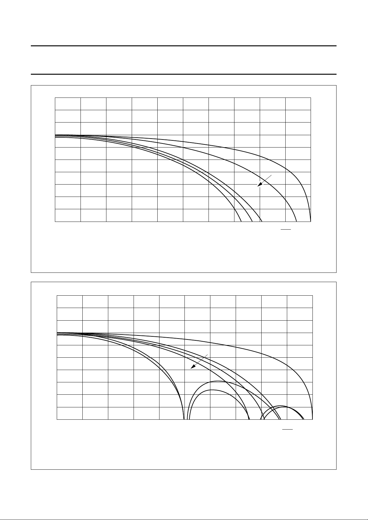
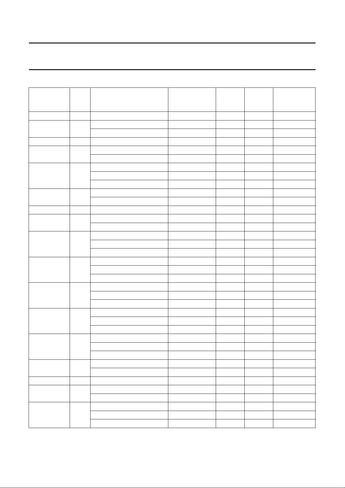
Figures 13 and 14 illustrate some frequency responses
2
and the corresponding I
C-bus settings.
The prefilter operates on 4 :4:4 YUV data. As U and V
are generated by simple chroma pixel doubling, the
UV prefilter should also be used to generate the
interpolated chroma values.
7.4.1.2 Subsampler
To improve the scaling performance for scales of less
1
⁄2 down to icon size, a FIR filtering subsampler is
than
available. It performs a subsampling of the incoming data
by a factor of 1/N (where N = XPSC + 1 = 1 to 64).
With N
equalling the number of input pixel/line and N
IP
OP
equalling the number of desired output pixels/line, the
basic equation to calculate XPSC is as follows:
N
IP
XPSC TRUNC
×=
-------------------NOP1–
The subsampler collects a number of [N + 1(−XACM)]
pixels to calculate a new subsampled output pixel.
Consequently, a downscale dependent FIR filter has been
incorporated, with up to 65 taps, which reduces aliasing for
small sizes. If XACM = 0 the collecting sequence overlaps,
which means that the last pixel of sequence M is also the
first pixel of sequence M + 1. To implement a real
subsampler bypass XACM has to be set to logic 1.
It should be noted that because the phase-correct
horizontal fine scaling is limited to a maximum downscale
of1⁄4, this circuitry has to be used for downscales less
than1⁄4 of the incoming pixel count.
To obtain unity gain at the subsamplers output for all
subsampling ratios, the I2C-bus parameters CXY, CXUV
and DCGX have to be used. In addition, the I2C-bus
parameters can be used to slightly modify the FIR
characteristic of the subsampler.
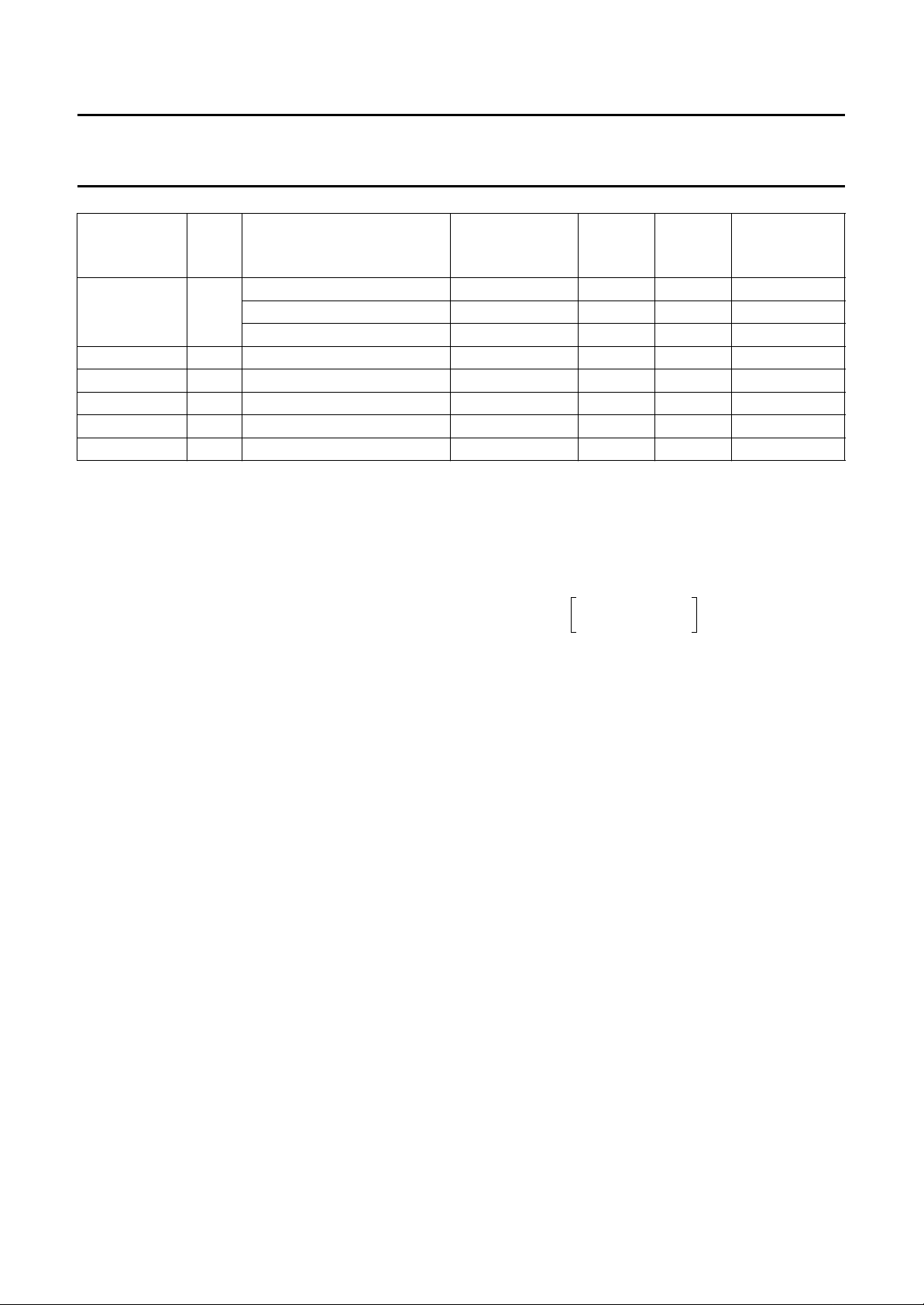
Table 1 gives examples of I2C-bus register settings,
depending on a given prescaler ratio. With reference to
Table 1, it should be noted that an internal
XPSC-dependent automatic prenormalization becomes
valid for XPSC > 8, > 6 and >32, which reduces the input
signal quantization. In addition, for XPSC ≥ 15 the LSB of
the CXY and CXUV parameter become valid.
1996 Sep 04 23
Page 24
Philips Semiconductors Objective specification
High Performance Scaler (HPS) SAA7140A; SAA7140B
18
handbook, full pagewidth
(Gain)
dB
6
0
–6
–18
–30
–42
0 0.1 0.2 0.3 0.4
I2C-bus bytes PFY3 to PFY0.
(1) = 0001; (2) = 0010; (3) = 0011; (4) = 1011; (5) = 1111.
Fig.13 Luminance prefilter frequency response for miscellaneous I2C-bus settings.
MHA121
(1)
(2)
(3)
(4)(5)
f
f
clk
0.5
18
handbook, full pagewidth
(Gain)
dB
6
0
–6
–18
(6)
–30
–42
0 0.1 0.2 0.3 0.4
I2C-bus bytes PFU3 to PFU0.
(1) = 0001; (2) = 0010; (3) = 1010; (4) = 1110; (5) = 0011; (6) = 1111.
Fig.14 Chrominance prefilter frequency response for miscellaneous I2C-bus settings.
MHA122
(1)
(5)
(2)
(4)
(3)
f
f
clk
0.5
1996 Sep 04 24
Page 25
Philips Semiconductors Objective specification
High Performance Scaler (HPS) SAA7140A; SAA7140B
Table 1 Horizontal prescaling and normalization
HORIZONTAL
PRESCALING
XPSC
COEFFICIENT SEQUENCE
(example)
CXY (luma)/
CXUV (chroma)
(HEX)
WEIGHT
SUM
DCGX
1 0 1-1 00 2 1 1
1
⁄
2
1 1-1-1 00 3 1
1-2-1 02 4 2 1
1
⁄
3
1
⁄
4
2 1-1-1-1 00 4 2 1
3 1-1-1-1-1 00 5 2
1-2-2-2-1 06 8 3 1
1
⁄
5
4111111 0062
121 121 02 8 3 1
112 211 04 8 3 1
1
⁄
6
5 1111111 00 7 3
1112111 08 8 3 1
1
⁄
7
1
⁄
8
611111111 00831
7 111111111 00 9 3
1222 2 2221 1E 16 7 1
1
⁄
9
8 1111111111 00
1221 2 2 1221 16
1122 2 2 2211 1C
1
⁄109 11111111111 00
1212 1 2 1 2121 2A
11122222111 38
1
⁄1110 1111 11 11 1111 00
1211 21 12 1121 12
111122 22 1111 30
1
⁄1211 1111 11 1 11 1111 00
1121 11 2 111211 44
1111 12 2 21 1111 60
1
⁄1312 11111111111111 00
1111211 112 1111 10
1111 112 221 1111 40
1
⁄1413 1111 111 1 111 1111 00
1111 111 2 111 1111 80
1
⁄1514 1111 1111 1111 1111 00
1
⁄1615 1111 1111 1 1111 1111
1222 2222 2 2222 2221 FF
1
⁄1716 1111 1111 1 1 1111 1111 00
1222 2222 1 1 2222 2221 FE
1222 2122 22 2212 2221 DF
10
⁄
2
16
⁄
2
16
⁄
2
11
⁄
2
16
⁄
2
16
⁄
2
12
⁄
2
16
⁄
2
16
⁄
2
13
⁄
2
16
⁄
2
16
⁄
2
14
⁄
2
16
⁄
2
16
⁄
2
15
⁄
2
16
⁄
2
16
⁄
2
17
⁄
2
32
⁄
2
18
⁄
4
32
⁄
4
32
⁄
4
2
31
31
2
31
31
2
31
31
2
31
31
2
31
31
2
31
31
3
71
2
31
31
BSC
(CONT/SAT)
=x/y×64
2
⁄
3
4
⁄
5
4
⁄
6
8
⁄
7
8
⁄
9
4
⁄
5
8
⁄
11
8
⁄
12
8
⁄
13
8
⁄
14
8
⁄
15
16
⁄
17
16
⁄
18
1996 Sep 04 25
Page 26
Philips Semiconductors Objective specification
High Performance Scaler (HPS) SAA7140A; SAA7140B
HORIZONTAL
PRESCALING
1
⁄
18
XPSC
17 1111111111111111111 00
COEFFICIENT SEQUENCE
(example)
1222 1222 1 2 1 2221 2221 EE
1222 211222221122221 9F
.... .... .... ....
1
⁄
33
32 1111 ... 1111 00
.... .... .... ....
1
⁄
63
1
⁄
64
62 .... .... .... .... ....
63 .... .... .... .... ....
7.4.2 VERTICAL SCALER
The vertical scaler performs the vertical downscaling of the
input data stream to a random number of output lines.
It can be used for input line lengths up to 768 pixels/line
and has to be bypassed if the input line length exceeds the
pixel count.
For vertical scaling there are two different modes
implemented; the ACCU mode (vertical accumulation) for
scales down to icon size and the Linear Phase
Interpolation mode (LPI) for scales between 1 and1⁄2.
7.4.2.1 ACCU mode (scaling factor range 1 to 1/1024;
2
C-bus bit YACM = 1:
I
The ACCU mode can be used for vertical scaling down to
icon size. In this mode, the I2C-bus parameter YSCI
controls the scaling and parameter YACL controls the
vertical anti-alias filtering.
The output lines are generated by a scale-dependent
variable averaging (YACL + 2) input lines. In this way a
vertical FIR filter can be created for anti-aliasing, with up to
65 taps (max.).
YSCI defines the output line qualifier pattern and YACL
defines the sequence length for the line averaging.
For accurate processing, the sequence has to fit into the
qualifying pattern. In the event of mis-programming YACL
unexpected line dropping occurs; where NOL= number of
output lines and NIL= number of input lines. The I2C-bus
bits YSCI (scaling increment), YACL (accumulation length;
optimum: 1 line overlap) and YP (scaling start phase) have
to be set according to the following equations (see Fig.15):
CXY (luma)/
CXUV (chroma)
(HEX)
YACL TRUNC
WEIGHT
SUM
19
⁄
4
32
⁄
4
32
⁄
4
xx
⁄
4
34
⁄
8
xx
⁄
8
N
IL
×=
------------------- NOL1–
DCGX
2
31
31
.... ....
2 −
.... ....
;
BSC
(CONT/SAT)
=x/y×64
16
⁄
19
accumulation sequence length: i.e. the number of lines per
sequence that are not part of overlay region of
neighbouring sequences (optimum 1 line overlapped).
–
1N
OL
YSCI INT 1024
YSCI
=
-------------- -
16
YP INT
×=
------------------- N
IL
; scaling start phase (fix; modified in
; scaling increment.
LPI mode only).
In order to obtain unity amplitude gain for all sequence
lengths and to improve the vertical scaling performance,
the accumulated lines can be weighted and the amplitude
of the scaled output signal has to be renormalized. In the
given example (see Fig.15) using the optimum weighting,
the gain of a sequence results in 1 + 2 + 2+1=6.
Renormalization (factor 1/6) can be achieved;
By gain reduction using BCS control (brightness,
contrast and saturation) down to
4
⁄6 and a selecting
factor of1⁄4 for DCGY2 to DCGY0 (see Section 8.3),
which may result in a loss of signal quantization, or
By gain emphasizing using BCS control up to8⁄6 and
selecting a factor of1⁄8 for DGY2 to DCGY0 which may
result in a loss of signal detail, due to limiting in the BCS
control.
Normally the weighting would be 2 + 2 + 2 + 2. In this
situation the gain can be renormalized with DCGY2
to DCGY0 = 010 (factor1⁄8).
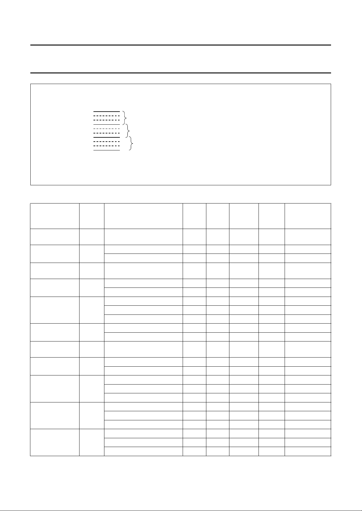
Table 2 gives examples for I2C-bus register settings,
depending on a given scale ratio.
1996 Sep 04 26
Page 27
Philips Semiconductors Objective specification
High Performance Scaler (HPS) SAA7140A; SAA7140B
handbook, full pagewidth
line 1
line 2
line 10
1st sequence
2nd sequence
3rd s equence
Fig.15 Example of vertical accumulation.
Table 2 Vertical scaling and normalization
VERTICAL
SCALE RATIO
(YSCI ≥)
1
⁄
1to
2
YACL
COEFFICIENT SEQUENCE
(example)
0 1-1 01 00 2 0 1
(0)
1
⁄2to1⁄
3
1 1-1-1 03 00 3 0
(512)
1
⁄3to1⁄
4
2 1-1-1-1 03 00 4 1 1
(683)
1
⁄4to1⁄
(768)
1
⁄5to1⁄
(820)
5
6
3 1-1-1-1-1 07 00 5 1
1-2-2-2-1 01 06 8 2 1
4111111070061
121 121 05 02 8 2 1
1 12 211 03 04 8 2 1
1
⁄6to1⁄
(854)
1
⁄7to1⁄
7
8
5 111 1 11 1 0F 00 7 2
1 11 2 11 1 07 08 8 2 1
6 1111 1111 0F 00 8 2 1
(878)
1
⁄8to1⁄
(896)
1
⁄9to1⁄
(91 1)
9
10
7 111111111 1F 00 9 2
1222 2 2221 01 1E 16 3 1
8 1111111111 1F 00 10 3
2121 2 2 1212 09 15 16 3 1
1122 2 2 2211 03 1C 16 3 1
1
⁄10to1⁄
(922)
11
9 111111 11111 3F 00 11 2
12121212121 15 2A 16 3 1
11122222111 07 38 16 3 1
1
⁄11to1⁄
(931)
12
10 1 1 11 11 11 1 1 1 1 3F 00 12 2
121 1 21 12 1 121 2D 12 16 3 1
1 1 1 1 22 22 11 1 1 0F 30 16 3 1
optimal weighting factors:
1
2
2
1
2
2
1
2
2
1
YACL = INT{(1-S)/S} = 2 (dotted lines)
YSCI = INT{(1024 × (1-S)} = 682
YP = INT{YSCI/16} = 42
CY A
(HEX)
CYB
(HEX)
WEIGHT
SUM
DCGY
MHA120
BCS
(CONT/SA T)
= x/y × 64
2
1-2-1 01 02 4 1 1
4
4
8
8
8
8
8
⁄
3
⁄
5
⁄
6
⁄
7
⁄
9
⁄
10
⁄
11
⁄
12
1996 Sep 04 27
Page 28
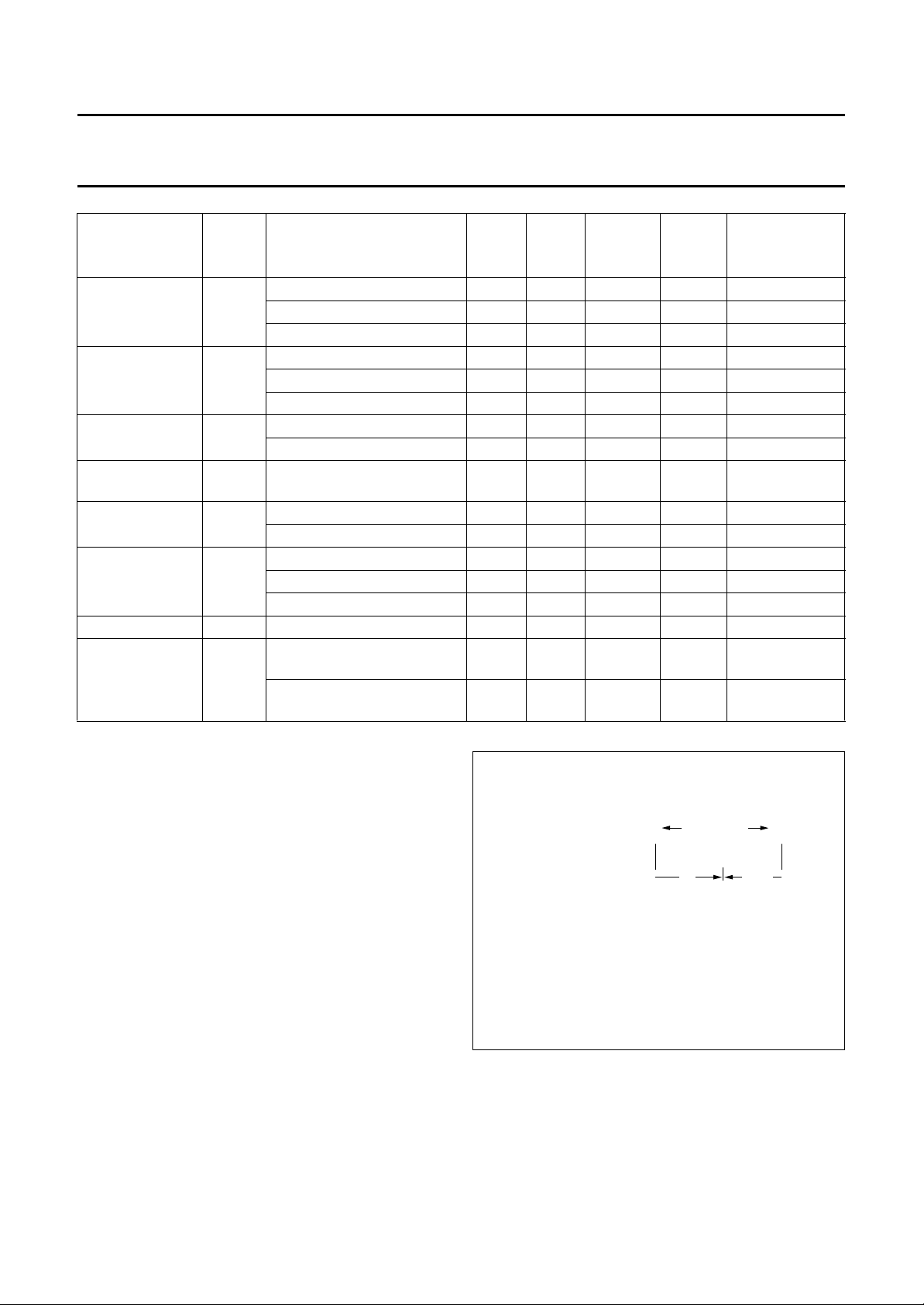
Philips Semiconductors Objective specification
High Performance Scaler (HPS) SAA7140A; SAA7140B
VERTICAL
SCALE RATIO
(YSCI ≥)
1
⁄12to1⁄
13
(939)
YACL
11 1111111111111 7F 00 13 2
COEFFICIENT SEQUENCE
(example)
CY A
(HEX)
CYB
(HEX)
WEIGHT
SUM
DCGY
1111 21 2 12 1111 2F 50 16 3 1
1121 11 2 111211 3B 44 16 3 1
1
⁄13to1⁄
(946)
14
12 1111 111 111 1111 7F 00 14 2
1111211 112 1111 6F 10 16 3 1
1111 112 211 1111 3F 40 16 3 1
1
⁄14to1⁄
(951)
1
⁄15to1⁄
15
16
13 1111 111 1 111 1111 FF 00 15 2
1111 111 2 111 1111 7F 80 16 3 1
14 1111 1111 1111 1111 FF 00 16 3 1
(956)
1
⁄16to1⁄
(960)
1
⁄17to1⁄
(964)
17
18
15 1111 1111 1 1111 1111 FF 00 17 3
2122 2222 2 2222 2212 02 FD 32 4 1
16 111111111111111111 FF 00 18 3
2212 2212 2 2 2122 2122 44 BB 32 4 1
1222 2222 1 1 2222 2221 01 FE 32 4 1
.... .... .... .... .... .... .... ....
1
⁄23to1⁄
(980)
24
22 1111 2222 1111
11112222 1111
1121 1212 1121
0F F0 32 4 1
AD 52 32 4 1
1211 2121 1211
BCS
(CONT/SA T)
= x/y × 64
8
⁄
13
8
⁄
14
8
⁄
15
16
⁄
17
16
⁄
18
7.4.2.2 LPI mode (scaling factor range 1 to
1
⁄
; IC-bus
2
bit YACM = 0)
To preserve the signal quality for slight vertical
downscales (scaling factors 1 to1⁄2) linear phase
interpolation between consecutive lines is implemented to
generate geometrically correct vertical output
lines.Therefore, the new geometric position between
lines N and N + 1 can be calculated.
A new output line is calculated by weighting the samples
‘p’ (pixel) of lines N and N + 1 with the normalized distance
to the new calculated position (see Fig.16);
When NOL= number of output lines and NIL= number of
input lines the I2C-bus bits YSCI (scaling increment) and
YP (scaling start phase) have to be set according to the
following equations;
handbook, halfpage
new calculated position
pM() ApN1+()1A–()pN()×+×=
where A = 0 to 63/64
Fig.16 New output line calculation.
input lines
of output line M
N distance = 1 N + 1
M
AA − 1
MHA361
1996 Sep 04 28
Page 29

Philips Semiconductors Objective specification
High Performance Scaler (HPS) SAA7140A; SAA7140B
YSCI INT 1024
YSCI
=
YP INT
-------------- -
16
IL
×=
---------N
OL
; scaling start phase
; scaling increment
1–
N
(recommended value).
YP
The vertical start phase offset is defined by
⁄
64
(YP = 0 to 64):
YP = 0: offset = 0 geometrical position of 1st line
out = 1st line in.
YP = 64: offset =64⁄64= 1 geometrical position of
1st line out = 2nd line in.
Finally 3 special modes must be emphasized:
1. By-pass (YSCI = 0, YP = 64) each line out is
equivalent to corresponding line in.
2. Low-pass (YSCI = 0, YP < 64) e.g. YP = 32: average
value of 2 lines (1 + z−H filter).
3. For processing of interlaced input signals the LPI
mode must be used (the ACCU mode would cause
‘line pairing’ problems). The scaling start phase for odd
and even field have to be set to:
YP
even
YP
odd
YSCI
+=
-------------- 32
;
where line 1 = odd.
In modes 1 and 2 the first input line is fed to the output
(without processing) so that the number of output lines
equals the number of input lines.
7.4.2.3 Flip option (FLIP = 1)
For both vertical scaling modes there is a flip option
(mirroring) available for input lines with a maximum of
384 pixels. In the event that full screen pictures (e.g.
768 × 576) are to be flipped, they first have to be scaled
down to 384 pixels per line in the horizontal prescaling
unit. After vertical processing (flipping) they can be
rezoomed to the original 768 pixels per line in the following
VPD. It should be noted that when using the flip option, the
last input line can not be displayed at the output.
The phase scaling consists of a filter and arithmetic
structure with 10 taps for the luminance and 4 taps for the
chrominance processing. It is able to generate a
phase-correct new pixel value, with virtually no phase or
amplitude artefacts.
The new samples are calculated with a phase accuracy
1
⁄64 of the pixel distance.
of
When using this circuit the up and down scaling is
controlled by the I2C-bus parameters XSCI and XP.
Because the variable phase scaling is restricted to
downscale >1⁄4 of the fine scalers input pixel count, XSCI
is also a function of the prescaling parameter XPSC.
As N
= number of input pixels per line (at SAA7140A
IP
input) and N
= number of desired output pixels/line,
OP
XSCI is defined by the following equation:
XSCI INT
N
---------- N
OP
IP
1024
×=
--------------------------------- XPSC 1+()
The maximum value of XSCI = 4095. Zooming is
performed for XSCI values less than 1024. The number of
disqualified clock cycles between consecutive pixel
qualifiers (at the phase scalers input) defines the
maximum possible zoom factor. This means that zooming
may also be a function of XPSC. It should be noted that
implementation is dependent on a zooming factor greater
than 2. Some artefacts may occur at the end of the
zoomed line.
Internal rounding effects, may result in a deviation of
±1 output pixels compared to the expected result. In this
situation, the I
2
C-bus parameter XP can be used to shift
the starting phase of the phase calculation and thereby
force an additional cycle to be disqualified.
In addition, when XP ≥ 128 it will force the internal phase
calculation to fixed values, especially when XP = 128 it will
force the phase scaler into bypass.
The scaled output data is fed back to the data
formatter/reformatter unit and may be used as output
signals from the bidirectional expansion port (if the mode
is selected).
7.4.3 H
ORIZONTAL VARIABLE PHASE SCALING
In the phase-correct horizontal variable phase scaling the
pixels are calculated for the geometrical correct,
orthogonal output pattern, down to1⁄4 of the prescaled
pattern. In addition, a horizontal zooming feature is
supported. The maximum zooming factor is at least 2, thus
being even more dependent on input pattern and
prescaling settings.
1996 Sep 04 29
7.5 Colour Space Matrix (CSM), dither and gamma
correction
The scaled YUV output data can be converted after
Interpolation into RGB data in accordance with CCIR 601
recommendations.
Page 30

Philips Semiconductors Objective specification
High Performance Scaler (HPS) SAA7140A; SAA7140B
The matrix equations considering the digital quantization
are as follows;
R = Y + 1.375 V
G=Y−0.703125 V − 0.34375 U
B = Y + 1.734375 U
For error diffusion a dither algorithm of the 5-bit truncation
error RGB (5, 5, 5) is implemented.
An anti-gamma characteristic (γ = 1.4) is implemented at
the matrix output to provide anti-gamma correction of the
RGB data. The curve can be used (bit RTB = 0) to
compensate gamma correction for linear data
representation of the RGB output data.
The chroma signal keyer generates an alpha signal to
achieve an RGB (5, 5, 5) + α output signal. Therefore, the
processed UV data amplitudes are compared with
thresholds set via the I2C-bus. A logic 1 signal is
generated if the amplitude is within the specified amplitude
range, if the amplitude is outside the specified range a
logic 0 is generated. Keying can be switched off by setting
the lower limit higher than the upper limit.
For 16-bit YUV data formats or monochrome modes the
CSM block is bypassed.
7.6 Output formatter and output FIFO register
In order to support various scaling applications, the output
data at the VRAM port can be delivered in different formats
and different transfer modes. Besides the 16-bit YUV
format (see Section 7.1.1) the VRAM port also supports
the data formats 24-bit RGB, 2 × 15-bit RGB + α or 8-bit
grey scale.
Should the synchronous data transfer mode (transparent
mode) be selected, the VRAM port will provide VCLK clock
(clock rate of LLC) and PXQ (polarity via programming) on
extra pins for use by the circuitry receiving the VRAM port
data stream.
To ease frame buffer applications, an asynchronous
transfer (burst or FIFO mode) can be selected. In this
mode the VRAM ports VCLK has to be provided from an
external source, with a maximum clock rate of 32 MHz.
Only valid data is collected and transported.
7.6.1 D
ATA FORMATS AND REFERENCE SIGNALS OF THE
VRAM PORT
7.6.1.2 24-bit RGB:
The resampled YUV samples are converted into RGB
(8 bits each). All three components have the same sample
rate as luminance Y. Anti-gamma correction is available
(programming). The alpha bit is generated as the chroma
key in the UV domain.
Two RGB representations (code meanings) are
supported:
1. The CCIR 601 orientated RGB representation defines
code 16 for black and code 235 for full saturation.
2. The graphics display orientated RGB representation
codes black with 00H and white with FFH.
This representation can be achieved by corresponding
programming of brightness (equals offset), contrast
and saturation (equals gain) in the YUV domain.
This format is used in the transparent mode and in the
FIFO mode (one pixel at a time).
7.6.1.3 15-bit RGB (5, 5, 5) +α in 2 bytes
The resampled YUV samples are converted into 24-bit
RGB. The following truncation to 5 bits is optionally
(programming) performed with dithering effect (error
diffusion). There are two representations (code meanings)
supported; CCIR and graphics display orientated (see
Section 7.6.1.2). The alpha bit is generated as chroma key
in the YUV domain. This format is used in the transparent
mode and in the FIFO mode (one pixel at a time, or two
pixels at a time). The ordering of RGB bits and bytes at the
VRAM port is identical to that of the SAA7196.
7.6.1.4 8-bit grey scale
This is simply a Y = luminance signal which can be
selected to be coded as binary, or all bits inverted.
This format is used in the transparent mode and in the
FIFO mode (1, 2 or 4 pixels at a time).
The horizontal sync output HGTV marks (source
independent) the range of the active video at the VRAM
port.
The vertical sync output VSYV (I2C-bus controlled polarity)
carries the vertical sync information for the VRAM port
output data (positive or negative pulse with a length of
4 lines). At the falling or rising edge of VSYV the FLDV
output is stable.
7.6.1.1 16-bit YUV
The ordering of YUV bits and bytes at the VRAM port is
identical to that of the SAA7196.
1996 Sep 04 30
(see Section 7.1.1)
Page 31
Philips Semiconductors Objective specification
High Performance Scaler (HPS) SAA7140A; SAA7140B
handbook, full pagewidth
If VCLK cycles occur at VOEN = HIGH the FIFO register is unchanged but the outputs VRO31 to VRO0 remain in the 3-state position.
(1) Only valid for non-zoomed data.
PIXCLK
(LLC/2)
FIFO memory
filling level
HFL
VCLK
VOEN
VRO(n)
78988766544
minimum 8 words
available in FIFO
maximum 32LLC
(16 PIXCLK)
(1)
1 transfer cycle
(8 VCLK cycles)
70 1 2 3 4 5 6 7
Fig.17 Output port transfer to VRAM at 32-bit data format without scaling.
MHA132
handbook, full pagewidth
INTERNAL
SIGNAL
HFL
INCADR
(1) Only available for interfaced processing at the beginning of an odd field.
line n
active
video
line n + 1
64LLC
last half-full request for line n
(1)
64LLC
(1)
10LLC
vertical reset pulse
Fig.18 Vertical reset timing of the VRAM port.
1996 Sep 04 31
vertical blanking
minimum set-up time
MHA123
line increment sequence (1)
Page 32

Philips Semiconductors Objective specification
High Performance Scaler (HPS) SAA7140A; SAA7140B
7.7 Data transfer modes
7.7.1 E
The expansion port is controlled by I2C-bus subaddresses
02 (22H) and 03 (23H).
The expansion port can be configured in a very flexible
way. Table 3 gives examples of the I2C-bus programming
for several expansion port configurations. SAA7196
compatible modes are marked as ‘xx96’ in the MODE
column. After reset the expansion port reference signal
inputs are set to the ‘xxIO’ pins.
After reset the expansion port reference signal inputs are
set to the ‘xxIO’ pins.
Pin FDIO can be used in the same way as the DIR pin of
the SAA7196 if the I2C-bus bit FLDC is set to logic 1.
More information concerning the control signals can be
found in Chapter 8. For correct application the user should
first decide about some global interface properties before
referring to this chapter such as:
XPANSION PORT MODES
• Does the application require separate input and output
reference signal lines, if yes then I
• Does the application need hardware controlled I/O
switching, if yes then I2C-bus bit FLDC = 1 and use of
pin FDIO or
• Does software controlled I/O switching (register set
controlled) the same job, if yes then I2C-bus bit
FLDC = 0
• Which signal path defines the clock system
• Which signal path is the synchronization master
• Is dynamic field-wise switching required or is the source
switching quite static, if static then do not be confused
about odd or even; use SREGS and IREGS before
referring to the I2C-bus section.
2
C-bus bit SRIO = 0
1996 Sep 04 32
Page 33
Philips Semiconductors Objective specification
High Performance Scaler (HPS) SAA7140A; SAA7140B
I/O
[SUBADDRESS 03 (23H)]
SCALER INPUT CONTROL
note 18
YUV8
MODE FDIO
FLDC VIDC VD1 VD0 HD1 HD0 PXQD LLCD SRIO VSI HSI VIPSI LLCS
24H
04 to
0 X00000000000000 note 1
1 X00100000000010 note 2
2 X001X1x10101111note 3
3 X001X1X10001110note 4
4 X00010101000000 note 5
5 X10010101000010 note 6
6 X10000000001111 note 7
7 X10010101101111 note 8
8 X00100000000110 note 9
9 X 1 01XXXXXX11111note 10
0’960 01000000010000note 11
DAVE OUTPUT CONTROL [SUBADDRESS 02 (22H)]
Table 3 Expansion port programming examples
1996 Sep 04 33
1’961 01000000010000note 12
2’961 0 11xXXXXX11111note 13
3’96x011xXX10011100note 14
4’961 01100XXX010110note 15
5’960 01000XXX010011note 16
6’961 01000XXX010011note 17
LLC, Y/UVIN, CREF, HREF and VS.
LLC, d.c., CREF, HREF and VS.
LLCIN, d.c., CREF, HIN and VIN.
LLC, d.c., CREF, HIN and VIN.
Notes
1. Scaler input from LLC, Y/UVIN, CREF, HREF and VS; expansion port output clock, data, qualifier, horizontal and vertical reference derived from
2. Scaler input from LLC, VIDH|L, PXQIN, HREF and VS; expansion port output clock, data, qualifier, horizontal and vertical reference derived from
3. Scaler input from LLCIN, VIDH|L, PXQIN, HIN and VIN; expansion port output clock, data, qualifier, horizontal and vertical reference derived from
4. Scaler input from LLC, VIDH|L, PXQIN, HIN and VIN; expansion port output clock, data, qualifier, horizontal and vertical reference derived from
Page 34

Philips Semiconductors Objective specification
High Performance Scaler (HPS) SAA7140A; SAA7140B
LLC, YUVsc, Psc, Hsc and Vsc.
YUVsc->VIDH, Psc, Hsc and Vsc.
LLC, Y|UVIN->VIDH, C+HREF and VS.
LLCIN, YUVsc->VIDH, Psc, Hsc and Vsc.
d.c., CREF, HREF and VS.
d.c., d.c., d.c., d.c. and d.c..
LLC, Y|UVIN, CREF, HREF and VS.
LLC, d.c., CREF, HREF and VS.
d.c., d.c., d.c., d.c. and d.c..
d.c., CREF, d.c. and d.c.
d.c., d.c., d.c., HREF and VS.
LLC, Y/UVIN, CREF, HREF and VS.
d.c., d.c., d.c., HREF and VS.
5. Scaler input from LLC, Y|UVIN, CREF, HREF and VS; expansion port output clock, data, qualifier, horizontal and vertical reference derived from
6. Scaler input from LLC, VIDL, PXQIN, HREF and VS; expansion port output clock, data, qualifier, horizontal and vertical reference derived from LLC,
7. Scaler input from LLCIN, VIDL, PXQIN, HIN and VIN; expansion port output clock, data, qualifier, horizontal and vertical reference derived from
8. Scaler input from LLCIN, VIDL PXQIN, HIN and VIN; expansion port output clock, data, qualifier, horizontal and vertical reference derived from
9. Scaler input from LLC, VIDH|L PXQIN, HIN and VS; expansion port output clock, data, qualifier, horizontal and vertical reference derived from LLC,
10. Scaler input from LLCIO, VIDH, PXQIO, HIO and VIO; expansion port output clock, data, qualifier, horizontal and vertical reference derived from
11. Scaler input from LLC, Y|UVIN, CREF, HREF and VS; expansion port output clock, data, qualifier, horizontal and vertical reference derived from
12. Scaler input from LLC, VIDH|L, CREF, HREF and VS; expansion port output clock, data, qualifier, horizontal and vertical reference derived from
13. Scaler input from LLCIO, VIDH|L, PXQIO, HIO and VIO; expansion port output clock, data, qualifier, horizontal and vertical reference derived from
14. Scaler input from LLC, VIDH|L, CREF, HIO and VIO; expansion port output clock, data, qualifier, horizontal and vertical reference derived from LLC,
15. Scaler input from LLC, VIDH/L, PXQIO, HIO and VS; expansion port output clock, data, qualifier, horizontal and vertical reference derived from LLC,
16. Scaler input from LLC, Y/UVIN, CREF, HREF and VS; expansion port output clock, data, qualifier, horizontal and vertical reference derived from
17. Scaler input from LLCIO, VIDH/L, PXQIO, HREF and VS; expansion port output clock, data, qualifier, horizontal and vertical reference derived from
18. Fill in user specific configuration.
1996 Sep 04 34
Page 35

Philips Semiconductors Objective specification
High Performance Scaler (HPS) SAA7140A; SAA7140B
7.8 VRAM port modes
7.8.1 D
ATA BURST TRANSFER MODE (FIFO MODE)
Data transfer on the VRAM port is asynchronous
(TTR = 0). This mode can be used for all output formats.
Four signals for communication with the external memory
are provided:
1. HFL flag: the half-full flag of the FIFO output register is
raised when the FIFO contains at least 8 data words
(HFL = HIGH). By setting HFL to logic 1, the
SAA7140A and SAA7140B requests a data burst
transfer, via the external memory controller, that has to
start a transfer cycle within the next 32LLC cycles for
32-bit long word modes (16LLC cycles for
16 and 24-bit modes). If there are pixels in the FIFO at
the end of the line, which are not transferred, the circuit
fills up the FIFO register with ‘fill pixels’ until it is
half-full and sets the HFL flag to request a data burst
transfer. After the transfer is completed, HFL is used in
combination with INCADR to indicate the line
increments.
2. The INCADR output signal is used in combination with
HFL to control horizontal and vertical address
generation for a memory controller. The pulse
sequence depends on field formats
(interlace/non-interlace or odd/even fields) and control
bits OF1 and OF0 (subaddress 01). This means that:
a) HFL = 1 at the rising edge of INCADR: the END OF
LINE is reached; request for line address
increment
b) HFL = 0 at the rising edge of INCADR: the END OF
FIELD/FRAME is reached; request for line and
pixel address reset
3. VCLK input signal to clock the FIFO register output
data VRO(n). New data is placed on the VRO(n) port
with the rising edge of VCLK (see Fig.17).
4. The VOEN input enables output data VRO(n).
The outputs are in 3-state mode at VOEN = HIGH.
VOEN changes only when VCLK is LOW. If VCLK
pulses are applied when VOEN is HIGH, the outputs
remain inactive but the FIFO register accepts the
pulses.
7.8.2 C
ONTINUOUS DATA TRANSFER MODE (TRANSPARENT
)
MODE
Data transfer on the VRAM port can be achieved
synchronously (TTR = 1), controlled by output reference
signals at separate pins (except the α-signal) and a
continuous clock output signal (clock rate of LLC) on the
VCLK pin.
The SAA7140A and SAA7140B delivers a continuously
processed data stream. Consequently, the extended
formats of the VRAM port output are selected (bit FS2 = 1;
see Tables 6 and 7).
The output reference signals have to be used to buffer
qualified preprocessed RGB or YUV video data. The YUV
data is only valid in qualified time slots. Control output
signals (see Tables 6 and 7) are:
•α= keying signal of the chroma keyer (not on extra pin
but in lower byte of VRO output)
• FLDV = odd/even field bit in accordance with the
internal field processing
• VSYV = vertical sync signal, active polarity is defined by
VSYP bit
• HGTV = horizontal gate signal, logic 1 marks the
horizontal direction from XO to (XO + XS) lines
• PXQV = pixel qualifier signal, active polarity is defined
by QPP bit.
Interlaced processing (OF bits, subaddress 01): to support
correctly interlaced data storage, the scaler delivers two
INCADR/HFL sequences in each qualified line and an
additional INCADR/HFL sequence after the vertical reset
sequence at the beginning of an odd field. Consequently,
the scaled lines are automatically stored in the right
sequence.
INCADR timing: the distance from the last half-full request
(HFL) to the INCADR pulse may be longer than 64LLC.
The state of HFL is defined for minimum 2LLC cycles
afterwards.
Monochrome format (see Tables 6 and 7); If TTR = 1 and
FS2 = 1 then Ya = Yb.
7.8.3 I
2
C-BUS CONTROLLED PSEUDO SLEEP MODE
To reduce the power consumption of the SAA7140A and
SAA7140B during phases, where no scaling operations
are requested in the application, it is possible to switch the
SAA7140A and SAA7140B into a pseudo sleep mode.
This mode can be activated, if the clock input LLCIN is not
used or if the hardware is able to pull the LLCIN input or
the LLCIO pin (in input mode) down to logic 0.
In applications, which do not use LLCIN, then LLCIN
should be connected to ground.
LLC has to be provided continuously.
1996 Sep 04 35
Page 36
Philips Semiconductors Objective specification
High Performance Scaler (HPS) SAA7140A; SAA7140B
To activate the ‘Sleep Mode’ the scalers processing has to
be switched to one of the inactive clock inputs of the
expansion port. For example, If LLCIO is used as input and
output in the application then:
LLCIN grounded => ‘Sleep Mode’ is active, if I2C-bus
To activate the scaler again, switch back to an active input
clock, via SRIO and/or LLCS.
In ‘Sleep Mode’ the power consumption of the SAA7140A
and SAA7140B is reduced to approximately 15% of its
normal operational value.
bits FLDC = 0, SRIO = 0 and LLCS = 1.
and If LLCIN is used as input and LLCIO is used as output:
LLCIN pulled down => ‘Sleep Mode’ is active, if I2C-bus
bits FLDC = 0, SRIO = 0 and LLCS = 1.
LLCIO pulled down => ‘Sleep Mode’ is active, if I2C-bus
bits FLDC = 0, SRIO = 1 and LLCS = 1.
Table 4 VRAM port output data formats (VRO31 to VRO16) at FS2 bit = 0 and VOF bit = 1 (can be set via I
burst mode only, Pixel order = n, n + 1, n + 2, etc.
FS1 = 0; FS0 = 0
PIXEL
OUTPUT
RGB (5, 5, 5) + α
32-BIT WORDS
(1)(2)
BITS
n n+2 n+4 n n+2 n+4 n n+1 n+2
VRO31 αααY
VRO30 R4 R4 R4 Y
VRO29 R3 R3 R3 Y
VRO28 R2 R2 R2 Y
VRO27 R1 R1 R1 Y
VRO26 R0 R0 R0 Y
VRO25 G4 G4 G4 Y
VRO24 G3 G3 G3 Y
VRO23 G2 G2 G2 U
VRO22 G1 G1 G1 U
VRO21 G0 G0 G0 U
VRO20 B4 B4 B4 U
VRO19 B3 B3 B3 U
VRO18 B2 B2 B2 U
VRO17 B1 B1 B1 U
VRO16 B0 B0 B0 U
FS1 = 0; FS0 = 1
YUV4:2:2
32-BIT WORDS
Y
e7
e6
e5
e4
e3
e2
e1
e0
e7
e6
e5
e4
e3
e2
e1
e0
e7
Y
e6
Y
e5
Y
e4
Y
e3
Y
e2
Y
e1
Y
e0
U
e7
U
e6
U
e5
U
e4
U
e3
U
e2
U
e1
U
e0
(2)(3)
Y
Y
Y
Y
Y
Y
Y
Y
U
U
U
U
U
U
U
U
FS1 = 1; FS0 = 0
YUV4:2:2
16-BIT WORDS
Y
e7
Y
e6
Y
e5
Y
e4
Y
e3
Y
e2
Y
e1
Y
e0
U
e7
U
e6
U
e5
U
e4
U
e3
U
e2
U
e1
U
e0
Y
e7
Y
e6
Y
e5
Y
e4
Y
e3
Y
e2
Y
e1
Y
e0
V
e7
V
e6
V
e5
V
e4
V
e3
V
e2
V
e1
V
e0
(2)(3)
Y
o7
o6
o5
o4
o3
o2
o1
o0
e7
e6
e5
e4
e3
e2
e1
e0
e7
Y
e6
Y
e5
Y
e4
Y
e3
Y
e2
Y
e1
Y
e0
U
e7
U
e6
U
e5
U
e4
U
e3
U
e2
U
e1
U
e0
FS1 = 1; FS0 = 1
8-BIT MONOCHROME
32-BIT WORDS
n
n+4
n+1
Y
Y
Y
Y
Y
Y
Y
Y
Y
Y
Y
Y
Y
Y
Y
Y
n+5
a7
a6
a5
a4
a3
a2
a1
a0
b7
b6
b5
b4
b3
b2
b1
b0
Y
a7
Y
a6
Y
a5
Y
a4
Y
a3
Y
a2
Y
a1
Y
a0
Y
b7
Y
b6
Y
b5
Y
b4
Y
b3
Y
b2
Y
b1
Y
b0
2
C-bus),
n+8
n+9
(4)
Y
Y
Y
Y
Y
Y
Y
Y
Y
Y
Y
Y
Y
Y
Y
Y
a7
a6
a5
a4
a3
a2
a1
a0
b7
b6
b5
b4
b3
b2
b1
b0
Notes
1. α = keying bit.
2. RGB and YUV = digital signals.
3. e = even pixel numbers.
4. a and b = consecutive pixels.
1996 Sep 04 36
Page 37
Philips Semiconductors Objective specification
High Performance Scaler (HPS) SAA7140A; SAA7140B
Table 5 VRAM port output data formats (VRO15 to VRO0) at FS2 bit = 0 and VOF bit = 1 (can be set via I2C-bus),
burst mode only, Pixel order = n, 1n, 2n, etc.
PIXEL
OUTPUT
FS1 = 0; FS0 = 0
RGB (5, 5, 5) + α
32-BIT WORDS
(1)(2)
FS1 = 0; FS0 = 1
YUV4:2:2
32-BIT WORDS
BITS
n + 1 n + 3 n + 5 n + 1 n + 3 n + 5 OUTPUT NOT USED
VRO15 αααY
VRO14 R4 R4 R4 Y
VRO13 R3 R3 R3 Y
VRO12 R2 R2 R2 Y
VRO11 R1 R1 R1 Y
VRO10 R0 R0 R0 Y
VRO9 G4 G4 G4 Y
VRO8 G3 G3 G3 Y
VRO7 G2 G2 G2 V
VRO6 G1 G1 G1 V
VRO5 G0 G0 G0 V
VRO4 B4 B4 B4 V
VRO3 B3 B3 B3 V
VRO2 B2 B2 B2 V
VRO1 B1 B1 B1 V
VRO0 B0 B0 B0 V
o7
o6
o5
o4
o3
o2
o1
o0
e7
e6
e5
e4
e3
e2
e1
e0
FS1 = 1; FS0 = 0
YUV4:2:2
(2)(3)(4)
Y
Y
Y
Y
Y
Y
Y
Y
V
V
V
V
V
V
V
V
Y
o7
o6
o5
o4
o3
o2
o1
o0
e7
e6
e5
e4
e3
e2
e1
e0
o7
Y
o6
Y
o5
Y
o4
Y
o3
Y
o2
Y
o1
Y
o0
V
e7
V
e6
V
e5
V
e4
V
e3
V
e2
V
e1
V
e0
16-BIT WORDS
XXXYc7Y
XXXYc6Y
XXXYc5Y
XXXYc4Y
XXXYc3Y
XXXYc2Y
XXXYc1Y
XXXYc0Y
XXXYd7Y
XXXYd6Y
XXXYd5Y
XXXYd4Y
XXXYd3Y
XXXYd2Y
XXXYd1Y
XXXYd0Y
(2)
FS1 = 1; FS0 = 1
8-BIT MONOCHROME
32-BIT WORDS
n+2
n+3
n+6
n+7
c7
c6
c5
c4
c3
c2
c1
c0
d7
d6
d5
d4
d3
d2
d1
d0
(5)
n+10
n+11
Y
c7
Y
c6
Y
c5
Y
c4
Y
c3
Y
c2
Y
c1
Y
c0
Y
d7
Y
d6
Y
d5
Y
d4
Y
d3
Y
d2
Y
d1
Y
d0
Notes
1. α = keying bit.
2. RGB and YUV = digital signals.
3. o = odd pixel numbers.
4. e = even pixel numbers.
5. c and d = consecutive pixels.
1996 Sep 04 37
Page 38
Philips Semiconductors Objective specification
High Performance Scaler (HPS) SAA7140A; SAA7140B
Table 6 VRAM port output data formats (VRO31 to VRO16) at FS2 bit = 1 and VOF bit = 1 (can be set via I2C-bus),
burst and transparent mode, Pixel order = n, n + 1, n + 2, etc.
PIXEL
OUTPUT
FS1 = 0; FS0 = 0
RGB (5, 5, 5) + α
16-BIT WORDS
(1)(2)
FS1 = 0; FS0 = 1
YUV4:2:2
16-BIT WORDS
BITS
n n+1 n+2 n n+1 n+2 n n+1 n+2
VRO31 αααY
VRO30 R4 R4 R4 Y
VRO29 R3 R3 R3 Y
VRO28 R2 R2 R2 Y
VRO27 R1 R1 R1 Y
VRO26 R0 R0 R0 Y
VRO25 G4 G4 G4 Y
VRO24 G3 G3 G3 Y
VRO23 G2 G2 G2 U
VRO22 G1 G1 G1 U
VRO21 G0 G0 G0 U
VRO20 B4 B4 B4 U
VRO19 B3 B3 B3 U
VRO18 B2 B2 B2 U
VRO17 B1 B1 B1 U
VRO16 B0 B0 B0 U
e7
e6
e5
e4
e3
e2
e1
e0
e7
e6
e5
e4
e3
e2
e1
e0
FS1 = 1; FS0 = 0
RGB (8, 8, 8)
(2)(3)
Y
Y
Y
Y
Y
Y
Y
Y
U
U
U
U
U
U
U
U
Y
e7
e6
e5
e4
e3
e2
e1
e0
e7
e6
e5
e4
e3
e2
e1
e0
e7
Y
e6
Y
e5
Y
e4
Y
e3
Y
e2
Y
e1
Y
e0
U
e7
U
e6
U
e5
U
e4
U
e3
U
e2
U
e1
U
e0
24-BIT WORDS
R7 R7 R7 Y
R6 R6 R6 Y
R5 R5 R5 Y
R4 R4 R4 Y
R3 R3 R3 Y
R2 R2 R2 Y
R1 R1 R1 Y
R0 R0 R0 Y
G7 G7 G7 Y
G6 G6 G6 Y
G5 G5 G5 Y
G4 G4 G4 Y
G3 G3 G3 Y
G2 G2 G2 Y
G1 G1 G1 Y
G0 G0 G0 Y
(2)
FS1 = 1; FS0 = 1
8-BIT MONOCHROME
16-BIT WORDS
n
n+2
n+1
n+3
a7
a6
a5
a4
a3
a2
a1
a0
b7
b6
b5
b4
b3
b2
b1
b0
Y
a7
Y
a6
Y
a5
Y
a4
Y
a3
Y
a2
Y
a1
Y
a0
Y
b7
Y
b6
Y
b5
Y
b4
Y
b3
Y
b2
Y
b1
Y
b0
(4)
n+4
n+5
Y
a7
Y
a6
Y
a5
Y
a4
Y
a3
Y
a2
Y
a1
Y
a0
Y
b7
Y
b6
Y
b5
Y
b4
Y
b3
Y
b2
Y
b1
Y
b0
Notes
1. α = keying bit.
2. RGB and YUV = digital signals.
3. e = even pixel numbers.
4. a and b = consecutive pixels.
1996 Sep 04 38
Page 39
Philips Semiconductors Objective specification
High Performance Scaler (HPS) SAA7140A; SAA7140B
Table 7 VRAM port output data formats (VRO15 to VRO0) at FS2 bit = 1 and VOF bit = 1 (can be set via I2C-bus),
burst and transparent mode, Pixel order = n, n + 1, n + 2, etc.
PIXEL
OUTPUT
BITS
FS1 = 0; FS0 = 0
RGB (5, 5, 5) + α
16-BIT WORDS
(1)(2)
n n+1 n+2 n n+1 n+2 n n+1 n+2
FS1 = 0; FS0 = 1
YUV4:2:2
16-BIT WORDS
(1)(2)
FS1 = 1; FS0 = 0
RGB (8, 8, 8)
24-BIT WORDS
(1)(2)
FS1 = 1; FS0 = 1
8-BIT MONOCHROME
16-BIT WORDS
n
n+2
n+1
n+3
(1)
n+4
n+5
VRO15 X X XXXXB7B7B7XXX
VRO140 X X XXXXB6B6B6XXX
VRO13 X X XXXXB5B5B5XXX
VRO12 X X XXXXB4B4B4XXX
VRO11 X X XXXXB3B3B3XXX
VRO10 X X XXXXB2B2B2XXX
VRO9 X X XXXXB1B1B1XXX
VRO8 X X XXXXB0B0B0XXX
VRO7 αααααααααααα
VRO6 (α) (α) (α) (α) (α) (α) (α) (α) (α) (α) (α) (α)
VRO5 (α) (α) (α) (α) (α) (α) (α) (α) (α) (α) (α) (α)
VRO4 (α) (α) (α) (α) (α) (α) (α) (α) (α) (α) (α) (α)
VRO3 (α) (α) (α) (α) (α) (α) (α) (α) (α) (α) (α) (α)
VRO2 (α) (α) (α) (α) (α) (α) (α) (α) (α) (α) (α) (α)
VRO1 (α) (α) (α) (α) (α) (α) (α) (α) (α) (α) (α) (α)
VRO0 (α) (α) (α) (α) (α) (α) (α) (α) (α) (α) (α) (α)
Notes
1. α = keying bit.
2. RGB = digital signals.
1996 Sep 04 39
Page 40
Philips Semiconductors Objective specification
High Performance Scaler (HPS) SAA7140A; SAA7140B
Table 8 Optional VRAM port output data formats (VRO31 to VRO16) at FS2 bit = 0 and VOF bit = 0 (can be set via
2
C-bus), burst mode only; Pixel order = n, n + 1, n + 2, etc.; VMUX = 1 or 0
I
FS1 = 0, FS0 = 0
RGB (5, 5, 5) + α
PIXEL
32-BIT LONG WORD
(1)(2)(3)
32-BIT LONG WORD
OUTPUT
BITS
n n+2 n n+2
101010101010
VRO31 α Z α ZY
VRO30 R4 Z R4 Z Y
VRO29 R3 Z R3 Z Y
VRO28 R2 Z R2 Z Y
VRO27 R1 Z R1 Z Y
VRO26 R0 Z R0 Z Y
VRO25 G4 Z G4 Z Y
VRO24 G3 Z G3 Z Y
VRO23 G2 Z G2 Z U
VRO22 G1 Z G1 Z U
VRO21 G0 Z G0 Z U
VRO20 B4 Z B4 Z U
VRO19 B3 Z B3 Z U
VRO18 B2 Z B2 Z U
VRO17 B1 Z B1 Z U
VRO16 B0 Z B0 Z U
e7
e6
e5
e4
e3
e2
e1
e0
e7
e6
e5
e4
e3
e2
e1
e0
FS1 = 0, FS0 = 1
YUV 4 :2:2
(2)(4)
FS1 = 1, FS0 = 1
8-BIT MONOCHROME
32-BIT LONG WORD
n
n+1
n+4
n+5
ZYe7ZYa7ZYa7Z
ZYe6ZYa6ZYa6Z
ZYe5ZYa5ZYa5Z
ZYe4ZYa4ZYa4Z
ZYe3ZYa3ZYa3Z
ZYe2ZYa2ZYa2Z
ZYe1ZYa1ZYa1Z
ZYe0ZYa0ZYa0Z
ZUe7ZYb7ZYb7Z
ZUe6ZYb6ZYb6Z
ZUe5ZYb5ZYb5Z
ZUe4ZYb4ZYb4Z
ZUe3ZYb3ZYb3Z
ZUe2ZYb2ZYb2Z
ZUe1ZYb1ZYb1Z
ZUe0ZYb0ZYb0Z
(5)
Notes
1. α = keying bit.
2. RGB and YUV = digital signals.
3. Z = high ohmic (3-state).
4. e = even pixel numbers.
5. a and b = consecutive pixels.
1996 Sep 04 40
Page 41
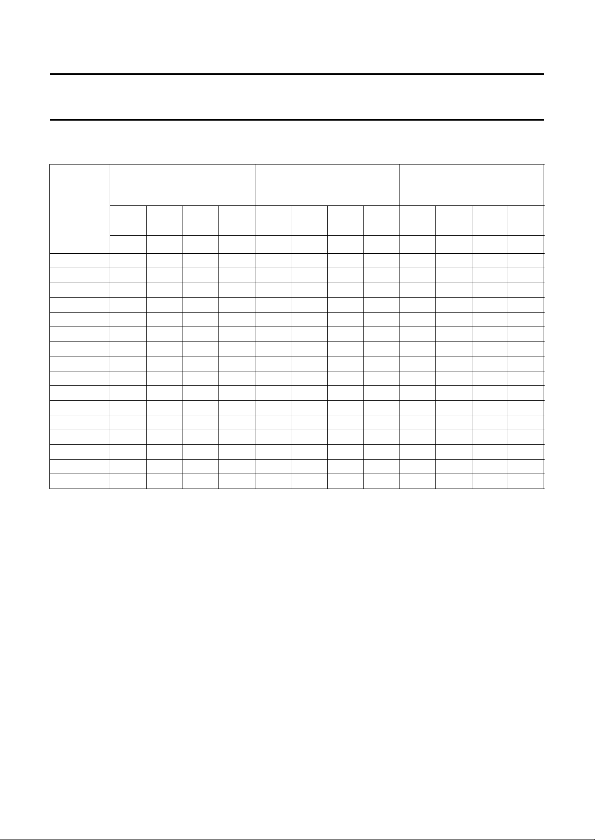
Philips Semiconductors Objective specification
High Performance Scaler (HPS) SAA7140A; SAA7140B
Table 9 Optional VRAM port output data formats (VRO15 to VRO0) at FS2 bit = 0 and VOF bit = 0 (can be set via
2
C-bus), burst mode only; Pixel order = n, n + 1, n + 2, etc.; VMUX = 1 or 0
I
PIXEL
FS1 = 0, FS0 = 0
RGB (5, 5, 5) + α
32-BIT LONG WORD
(1)(2)(3)
FS1 = 0, FS0 = 1
YUV 4 :2:2
32-BIT LONG WORD
OUTPUT
BITS
n+1 n+3 n+1 n+3
101010101010
VRO15 Z α Z α ZY
VRO14 Z R4 Z R4 Z Y
VRO13 Z R3 Z R3 Z Y
VRO12 Z R2 Z R2 Z Y
VRO11 Z R1 Z R1 Z Y
VRO10 Z R0 Z R0 Z Y
VRO9 Z G4 Z G4 Z Y
VRO8 Z G3 Z G3 Z Y
VRO7 Z G2 Z G2 Z V
VRO6 Z G1 Z G1 Z V
VRO5 Z G0 Z G0 Z V
VRO4 Z B4 Z B4 Z V
VRO3 Z B3 Z B3 Z V
VRO2 Z B2 Z B2 Z V
VRO1 Z B1 Z B1 Z V
VRO0 Z B0 Z B0 Z V
o7
o6
o5
o4
o3
o2
o1
o0
e7
e6
e5
e4
e3
e2
e1
e0
FS1 = 1, FS0 = 1
8-BIT MONOCHROME
(2)(3)(4)(5)
32-BIT LONG WORD
n+2
n+3
ZYo7ZYc7ZY
ZYo6ZYc6ZY
ZYo5ZYc5ZY
ZYo4ZYc4ZY
ZYo3ZYc3ZY
ZYo2ZYc2ZY
ZYo1ZYc1ZY
ZYo0ZYc0ZY
ZVe7ZYd7ZY
ZVe6ZYd6ZY
ZVe5ZYd5ZY
ZVe4ZYd4ZY
ZVe3ZYd3ZY
ZVe2ZYd2ZY
ZVe1ZYd1ZY
ZVe0ZYd0ZY
(3)(6)
n+6
n+7
c7
c6
c5
c4
c3
c2
c1
c0
d7
d6
d5
d4
d3
d2
d1
d0
Notes
1. α = keying bit.
2. RGB and YUV = digital signals.
3. Z = high ohmic (3-state).
4. o = odd pixel numbers.
5. e = even pixel number.
6. c and d = consecutive pixels.
1996 Sep 04 41
Page 42
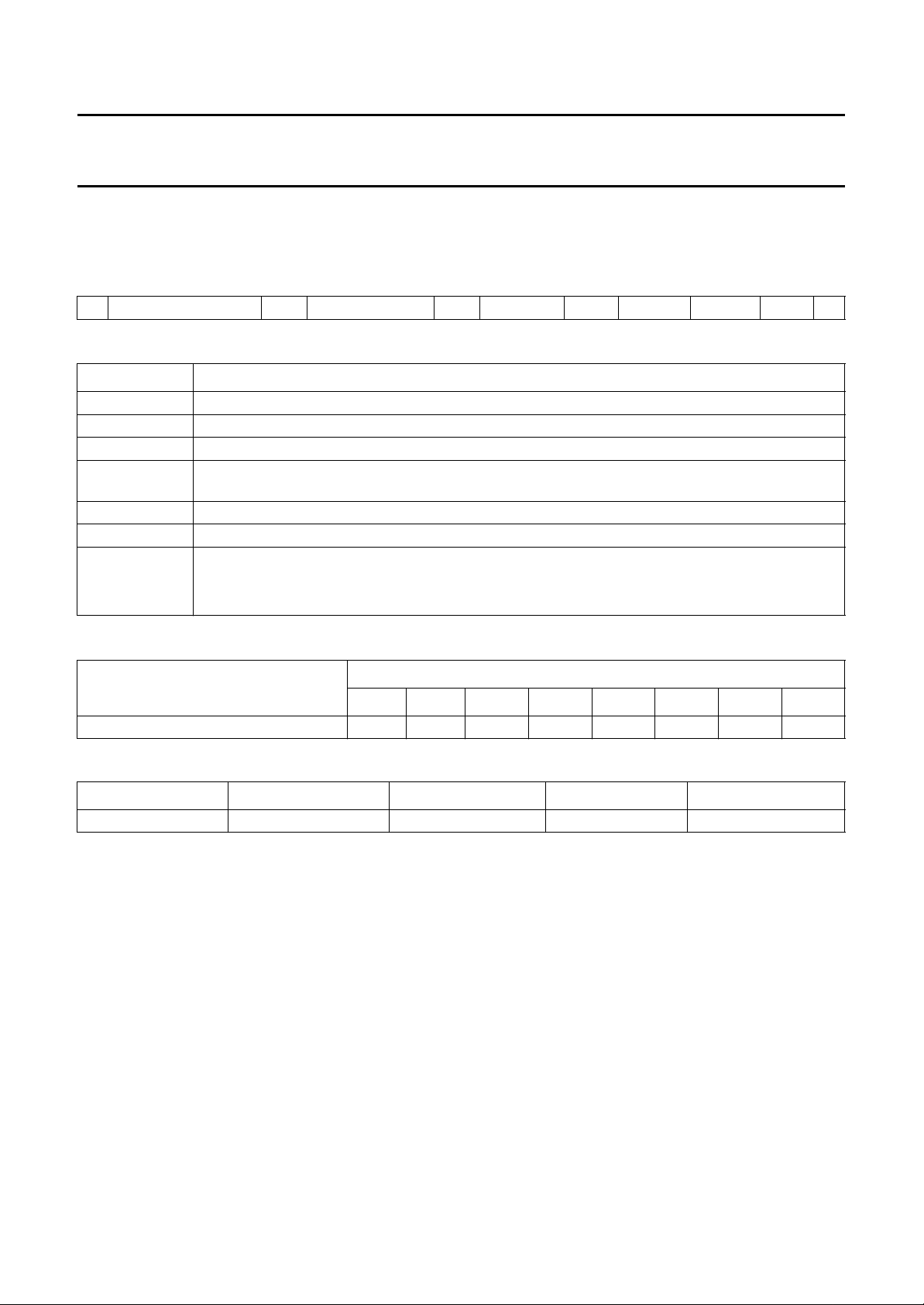
Philips Semiconductors Objective specification
High Performance Scaler (HPS) SAA7140A; SAA7140B
8I2C-BUS PROTOCOL
2
8.1 I
Table 10 I
Table 11 Description of I
S START condition
Slave address 0111 00X = IICSA = LOW or 0111 001X = IICSA = HIGH
ACK acknowledge generated by the slave
Subaddress subaddress byte (if more than 1 data byte is transmitted then an auto-increment of the subaddress
Data data byte
P STOP condition
X read/write control bit:
C-bus format
2
C-bus format
S SLAVE ADDRESS ACK SUBADDRESS ACK DATA0 ACK X DATAn ACK P
2
C-bus format
CODE DESCRIPTION
is performed)
X = 0, order to write (the circuit is slave receiver)
X = 1, order to read (the circuit is slave transmitter)
2
Table 12 I
C-bus status byte (X in address byte = 1; 71H at IICSA = LOW or 73H at IICSA = HIGH)
DATA BITS
FUNCTION
D7 D6 D5 D4 D3 D2 D1 D0
Status byte (subaddress 20H) ID3 ID2 ID1 ID0 X X X X
Table 13 Function of status bits ID3 to ID0 (software model of SAA7140A and SAA7140B compatible)
ID3 ID2 ID1 ID0 VERSION
0 0 0 0 V0 (first version)
2
Remark: With the exception of subaddress 20H (read only) all I
C-bus registers are read/write registers.
1996 Sep 04 42
Page 43
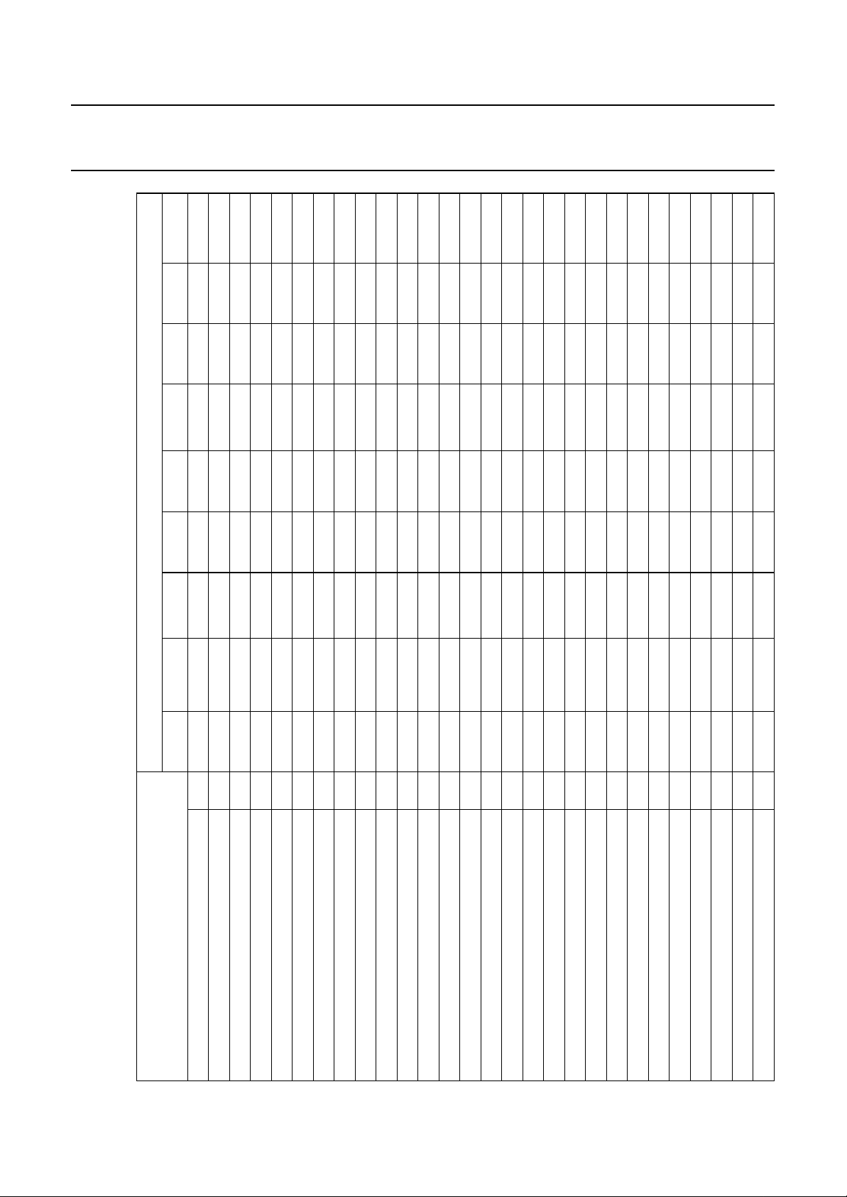
Philips Semiconductors Objective specification
High Performance Scaler (HPS) SAA7140A; SAA7140B
(1)
DATA BITS
D7 D6 D5 D4 D3 D2 D1 D0 DF
SREGS IREGS INVOE REVFLD FICO1 FICO0
(4)
(4)
VOF QPP OF1 OF0 LW1 LW0
REHAW REVAW VSI HSI VIPSI LLCS
(4)
SRIO
(4)
08 XO7 XO6 XO5 XO4 XO3 XO2 XO1 XO0
(2)
09 XS7 XS6 XS5 XS4 XS3 XS2 XS1 XS0
(2)
0C YO7 YO6 YO5 YO4 YO3 YO2 YO1 YO0
(3)
0D YS7 YS6 YS5 YS4 YS3 YS2 YS1 YS0
(3)
YP5 YP4 YP3 YP2 YP1 YP0
(4)
XPSC5 XPSC4 XPSC3 XPSC2 XPSC1 XPSC0
(4)
C-bus decoder control; subaddress and data bytes for writing (X in address byte = 0; 70H at IICSA = LOW or 72H at IICSA = HIGH);
2
C-bus bitmap
2
Table 14 I
8.2 I
FUNCTION SUBADDRESS
programming set A: subaddress = 02H to 1FH
Initial settings expansion/DMSD 00 FSEL RSEN
Initial settings VRAM 01 VPE TTR
Expansion port output control 02 FLDC VIDC VD1 VD0 HD1 HD0 PXQD LLCD
Expansion I/O control; scaler source control 03 VSYP
Expansion/VRAM format control 04 SHVS YUV8 MCT RTB DIT FS2 FS1 FS0
Luminance brightness 05 BRIG7 BRIG6 BRIG5 BRIG4 BRIG3 BRIG2 BRIG1 BRIG0
Luminance contrast 06 X CONT6 CONT5 CONT4 CONT3 CONT2 CONT1 CONT0
Chroma saturation 07 X SATN6 SATN5 SATN4 SATN3 SATN2 SATN1 SATN0
Horizontal window start
Horizontal window length
(continue) 0A X XO10 XO9 XO8 X XS10 XS9 XS8
1996 Sep 04 43
Vertical window length
Horizontal phase offset 0B XP7 XP6 XP5 XP4 XP3 XP2 XP1 XP0
(continue) 0E X YO10 YO9 YO8 X YS10 YS9 YS8
Vertical window start
Vertical phase offset 0F X YP6
Horizontal prescaling 10 X XACM
Horizontal weighting control (select Y) 11 CXY7 CXY6 CXY5 CXY4 CXY3 CXY2 CXY1 CXY0
Horizontal weighting control (select UV) 12 CXUV7 CXUV6 CXUV5 CXUV4 CXUV3 CXUV2 CXUV1 CXUV0
Prefilter YUV 13 PFUV3 PFUV2 PFUV1 PFUV0 PFY3 PFY2 PFY1 PFY0
Vertical interpolation control 14 FLIP YACM YACL5 YACL4 YACL3 YACL2 YACL1 YACL0
Vertical weighting control 1 15 CYA7 CYA6 CYA5 CYA4 CYA3 CYA2 CYA1 CYA0
Vertical weighting control 2 16 CYB7 CYB6 CYB5 CYB4 CYB3 CYB2 CYB1 CYB0
DC gain normalization 17 X DCGX2 DCGX1 DCGX0 X DCGY2 DCGY1 DCGY0
Horizontal scaling increment 18 XSCI7 XSCI6 XSCI5 XSCI4 XSCI3 XSCI2 XSCI1 XSCI0
(continue) 19 X X X X XSCI11 XSCI10 XSCI9 XSCI8
Vertical scaling increment 1A YSCI7 YSCI6 YSCI5 YSCI4 YSCI3 YSCI2 YSCI1 YSCI0
(continue) 1B X X X X X X YSCI9 YSCI8
Page 44
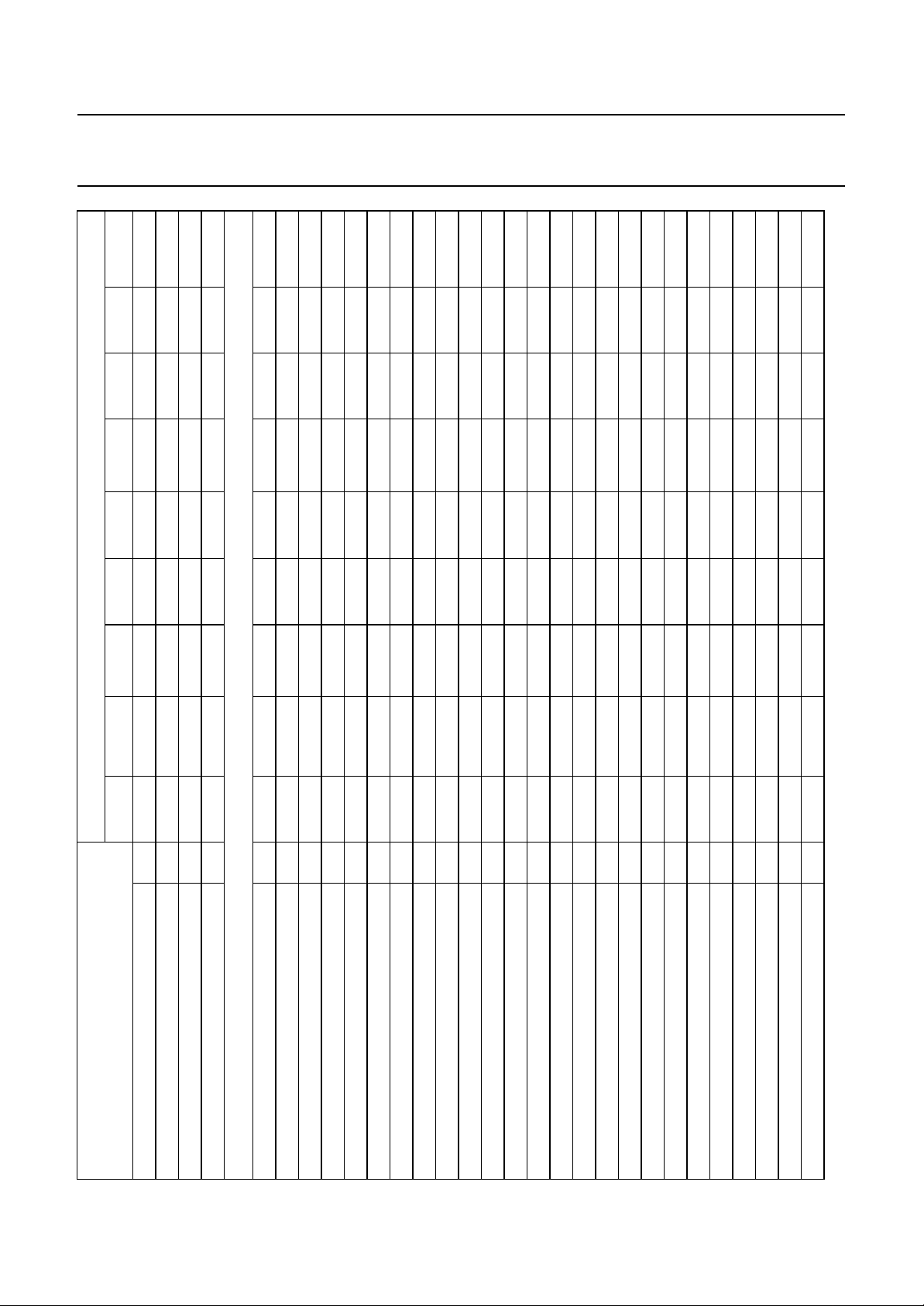
Philips Semiconductors Objective specification
High Performance Scaler (HPS) SAA7140A; SAA7140B
(1)
DATA BITS
D7 D6 D5 D4 D3 D2 D1 D0 DF
PORT3 PORT2 PORT1 PORT0
(4)
PEN0
(4)
PEN1
(4)
PEN2
(4)
REHAW REVAW VSI HSI VIPSI LLCS
(4)
SRIO
(4)
28 XO7 XO6 XO5 XO4 XO3 XO2 XO1 XO0
29 XS7 XS6 XS5 XS4 XS3 XS2 XS1 XS0
2C YO7 YO6 YO5 YO4 YO3 YO2 YO1 YO0
2D YS7 YS6 YS5 YS4 YS3 YS2 YS1 YS0
YP5 YP4 YP3 YP2 YP1 YP0
(4)
XPSC5 XPSC4 XPSC3 XPSC2 XPSC1 XPSC0
(4)
(5)
FUNCTION SUBADDRESS
Expansion port output control 22 FLDC VIDC VD1 VD0 HD1 HD0 PXQD LLCD
Expansion I/O control; scaler source control 23 VSYP
Expansion/VRAM format control 24 SHVS YUV8 MCT RTB DIT FS2 FS1 FS0
Luminance brightness 25 BRIG7 BRIG6 BRIG5 BRIG4 BRIG3 BRIG2 BRIG1 BRIG0
Luminance contrast 26 X CONT6 CONT5 CONT4 CONT3 CONT2 CONT1 CONT0
Chroma saturation 27 X SATN6 SATN5 SATN4 SATN3 SATN2 SATN1 SATN0
Chroma keying upper limit for V 1C VU7 VU6 VU5 VU4 VU3 VU2 VU1 VU0
Chroma keying lower limit for V 1D VL7 VL6 VL5 VL4 VL3 VL2 VL1 VL0
Chroma keying upper limit for U 1E UU7 UU6 UU5 UU4 UU3 UU2 UU1 UU0
Chroma keying lower limit for U 1F UL7 UL6 UL5 UL4 UL3 UL2 UL1 UL0
Programming set B; subaddress = 22H to 3FH
Read only register 20 ID3 ID2 ID1 ID0 X X X X
I/O port enable 21 PEN3
Horizontal window start
1996 Sep 04 44
(5)
(6)
(6)
Vertical window length
(continue) 2E X YO10 YO9 YO8 X YS10 YS9 YS8
Horizontal window length
(continue) 2A X XO10 XO9 XO8 X XS10 XS9 XS8
Horizontal phase offset 2B XP7 XP6 XP5 XP4 XP3 XP2 XP1 XP0
Vertical window start
Vertical phase offset 2F YPF YP6
Horizontal prescaling 30 X XACM
Horizontal weighting control (select Y) 31 CXY7 CXY6 CXY5 CXY4 CXY3 CXY2 CXY1 CXY0
Horizontal weighting control (select UV) 32 CXUV7 CXUV6 CXUV5 CXUV4 CXUV3 CXUV2 CXUV1 CXUV0
Prefilter YUV 33 PFUV3 PFUV2 PFUV1 PFUV0 PFY3 PFY2 PFY1 PFY0
Vertical interpolation control 34 FLIP YACM YACL5 YACL4 YACL3 YACL2 YACL1 YACL0
Vertical weighting control 1 35 CYA7 CYA6 CYA5 CYA4 CYA3 CYA2 CYA1 CYA0
Vertical weighting control 2 36 CYB7 CYB6 CYB5 CYB4 CYB3 CYB2 CYB1 CYB0
DC gain normalization 37 X DCGX2 DCGX1 DCGX0 X DCGY2 DCGY1 DCGY0
Horizontal scaling increment 38 XSCI7 XSCI6 XSCI5 XSCI4 XSCI3 XSCI2 XSCI1 XSCI0
Page 45
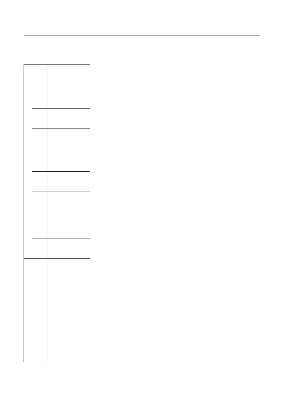
Philips Semiconductors Objective specification
High Performance Scaler (HPS) SAA7140A; SAA7140B
(1)
DATA BITS
D7 D6 D5 D4 D3 D2 D1 D0 DF
FUNCTION SUBADDRESS
(continue) 39 X X X X XSCI11 XSCI10 XSCI9 XSCI8
Vertical scaling increment 3A YSCI7 YSCI6 YSCI5 YSCI4 YSCI3 YSCI2 YSCI1 YSCI0
(continue) 3B X X X X X X YSCI9 YSCI8
Chroma keying upper limit for V 3C VU7 VU6 VU5 VU4 VU3 VU2 VU1 VU0
Chroma keying lower limit for V 3D VL7 VL6 VL5 VL4 VL3 VL2 VL1 VL0
Chroma keying upper limit for U 3E UU7 UU6 UU5 UU4 UU3 UU2 UU1 UU0
Chroma keying lower limit for U 3F UL7 UL6 UL5 UL4 UL3 UL2 UL1 UL0
Notes
1. Default register contents to be filled in by hand.
2. Continued in 0A.
3. Continued in 0E.
4. Bits set to logic 1 after reset (all other bits set to logic 0 after reset).
5. Continued in 2A.
6. Continued in 2E.
1996 Sep 04 45
Page 46
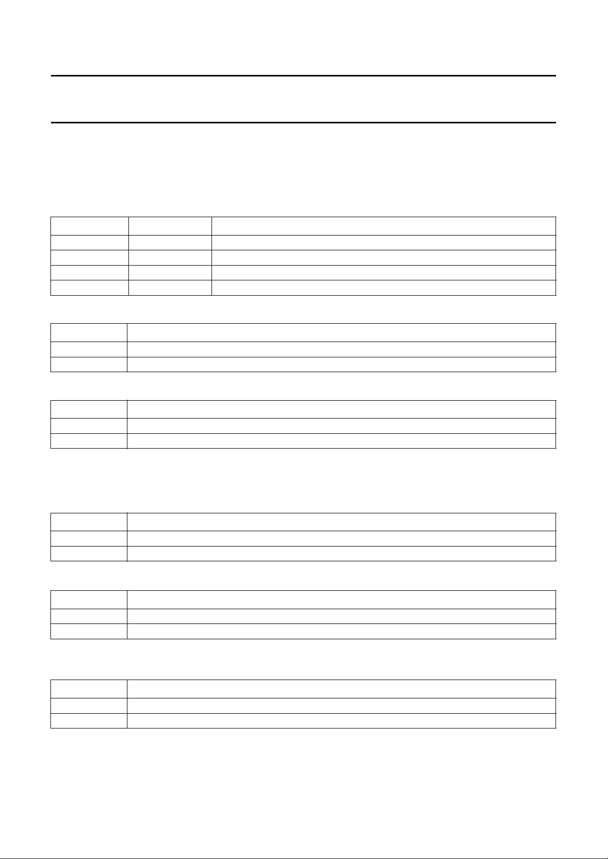
Philips Semiconductors Objective specification
High Performance Scaler (HPS) SAA7140A; SAA7140B
8.3 Description of the I2C-bus bits
Tables 15 to 21 give the function of the register bits given in Table 14.
8.3.1 I
NITIAL SETTINGS FOR THE EXPANSION AND DMSD PORT; SUBADDRESS 00H
Table 15 Field detection; data bits FICO1 to FICO0
FICO1 FICO0 DESCRIPTION
0 0 field sequence as detected from H and V sync signals
0 1 field sequence synchronized to H and V but noise limited
1 0 free running field sequence
1 1 reserved
Table 16 Reference edge selection for the V sync input of the field detection; data bit REVFLD
REVFLD DESCRIPTION
0 rising edge is reference
1 falling edge is reference
Table 17 Polarity selection for the H sync input of the field detection (note 1); data bit INVOE
INVOE DESCRIPTION
0 active LOW, e.g. for SAA71xx signals similar to HREF
1 active HIGH, e.g. for SAA71xx signals similar to HS
Note
1. INVOE may also be used for FDIO and FLDV output signal inversion
Table 18 Polarity of I
2
C-bus register set ID; data bit IREGS
IREGS DESCRIPTION
0 register set ID as defined by SREGS
1 register set ID inverted
2
Table 19 Fix I
C-bus register set ID; data bit SREGS
SREGS DESCRIPTION
0 register set ID toggles as detected and defined by FICO0 and FICO1
1 register set ID fixed to 1 (register set B selected)
Table 20 Enable of reference signals PXQIO, HIO, VIO, FDIO, LLCIO (expansion port) and PXQV , HGTV, VSYV, FLDV
(VRAM port); data bit RSEN
RSEN DESCRIPTION
0 reference signals enabled
1 reference signals disabled
1996 Sep 04 46
Page 47
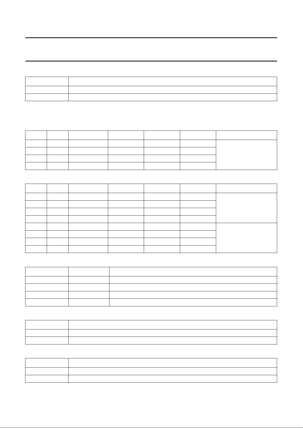
Philips Semiconductors Objective specification
High Performance Scaler (HPS) SAA7140A; SAA7140B
Table 21 Field sync definition; data bit FSEL
FSEL DESCRIPTION
0 V input for field detection to be handled as V sync signal
1 V input for field detection to be handled as frame sync signal
8.3.2 I
Table 22 First pixel position in VRO data for FS1 = 0; FS0 = 0 (RGB) and FS1 = 0; FS0 = 1 (YUV); data bits
Table 23 First pixel position in VRO data for FS1 = 1; FS0 = 1 (monochrome)
NITIAL SETTINGS FOR THE VRAM PORT; SUBADDRESS 01H
LW1 and LW0
LW1 LW0 BITS 31 to 24 BITS 23 to 16 BITS 15 to 8 BITS 7 to 0 REMARK
0 0 pixel 0 pixel 0 pixel 1 pixel 1
0 1 pixel 0 pixel 0 pixel 1 pixel 1
1 0 black black pixel 0 pixel 0
1 1 black black pixel 0 pixel 0
LW1 LW0 BITS 31 to 24 BITS 23 to 16 BITS 15 to 8 BITS 7 to 0 REMARK
0 0 pixel 0 pixel 1 pixel 2 pixel 3
0 1 black pixel 0 pixel 1 pixel 2
1 0 black black pixel 0 pixel 1
1 1 black black black pixel 0
0 0 pixel 0 pixel 1 X X
0 1 black pixel 0 X X
1 0 pixel 0 pixel 1 X X
1 1 black pixel 0 X X
FS2 = 0; TTR = 0
FS2 = 0; TTR = 0
FS2 = 1; TTR = 0;
LW only affects the grey
scale format
Table 24 Set output field mode; data bits OF1 to OF0
OF1 OF0 DESCRIPTION
0 0 both fields for interlaced storage
0 1 both fields for non-interlaced storage
1 0 odd fields only (even fields ignored) for non-interlaced storage
1 1 even fields only (odd fields ignored) for non-interlaced storage
Table 25 Pixel qualifier polarity flag; data bit QPP
QPP DESCRIPTION
0 PXQV is active LOW (pin 41)
1 PXQV is active HIGH
Table 26 VRAM-port output format; data bit VOF
VOF DESCRIPTION
0 enabling of 32 to 16-bit multiplexing via VMUX
1 disabling of 32 to 16-bit multiplexing via VMUX
1996 Sep 04 47
Page 48
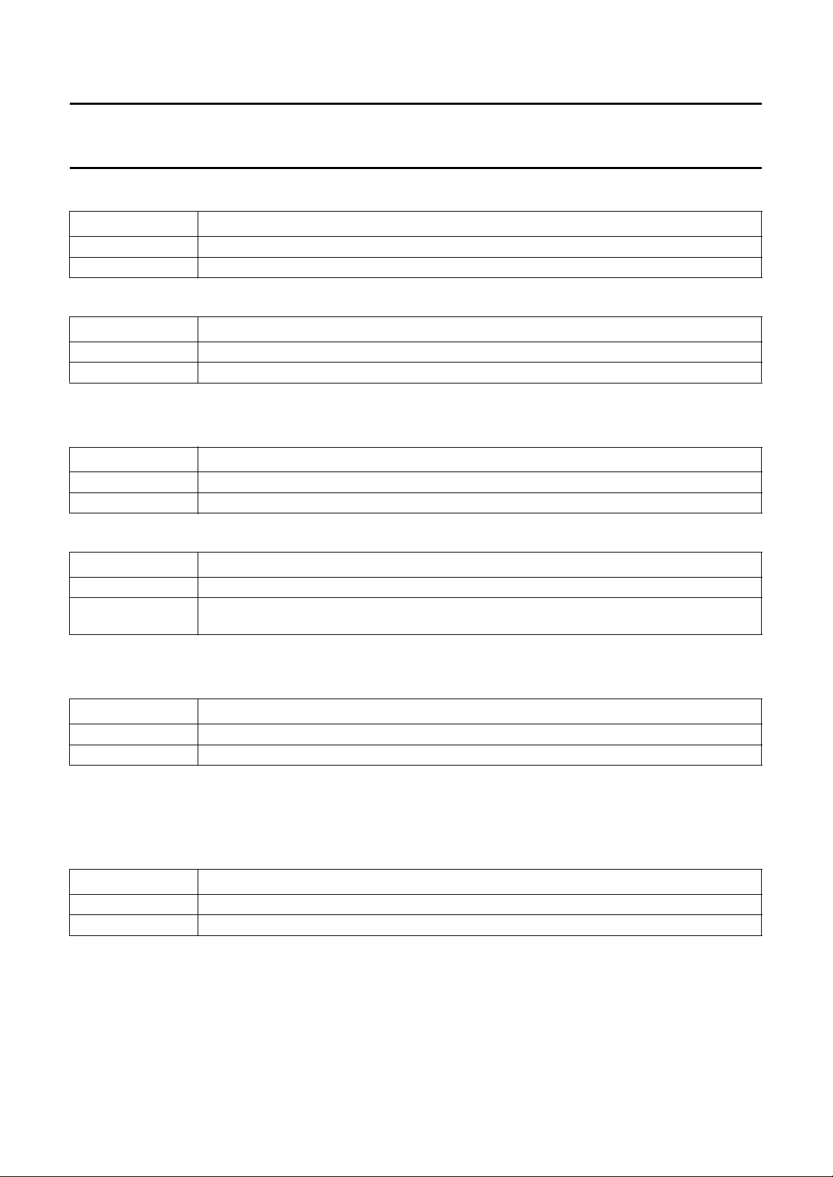
Philips Semiconductors Objective specification
High Performance Scaler (HPS) SAA7140A; SAA7140B
Table 27 VRAM-port mode selection; data bit TTR
TTR DESCRIPTION
0 FIFO mode (VRAM data burst transfer)
1 transparent mode
Table 28 VRAM-port outputs enable; data bit VPE
VPE DESCRIPTION
0 HFL and INCADR inactive (HFL = LOW, INCADR = HIGH); VRO outputs in 3-state
1 HFL and INCADR enabled; VRO outputs dependent on VOEN
8.3.3 P
ORT I/O CONTROL; SUBADDRESS 21H
Table 29 Select direction of PORT3 to PORT0; data bits PEN3 to PEN0
PEN3 TO PEN0 DESCRIPTION
PENx = 0 PORTx set to output
PENx = 1 PORTx set to input
Table 30 Status of port I/O’s, pins 32 (PORT3) to 35 (PORT0)
PORT3 to PORT0 DESCRIPTION
Write mode set status of PORT3 to PORT0 registers (applied to pins 32 to 35 if PENx = 0)
Read mode read status of PORT3 to PORT0; if PENx = 0 then status of PORTx register; if PENx = 1 then
status of external driven data
8.3.4 R
EGISTER SET A (02H TO 1FH) AND B (22H TO 3FH)
Table 31 Source select for expansion port clock output LLCIO (note 1 ); data bit LLCD
LLCD DESCRIPTION
0 source is clock from DMSD port
1 source is clock input from expansion port, as defined by SRIO
Note
2
1. The clock output on LLCIO may be disabled by I
C-bus bits SRIO = 1 and LLCS = 1; see Table 37.
Table 32 Source select for expansion port pixel qualifier and data output at PXQIO and VIDH/VIDL[7 to 0] (note 1);
data bit PXQD
PXQD DESCRIPTION
0 sources are corresponding signals from DMSD port
1 sources are corresponding signals from scaler output
Note
1. The qualifier output on PXQIO may be disabled by I
2
C-bus bits SRIO = 1 and VIPSI = 1; see Table 38.
1996 Sep 04 48
Page 49
Philips Semiconductors Objective specification
High Performance Scaler (HPS) SAA7140A; SAA7140B
Table 33 Source select for expansion port horizontal sync output HIO (note 1); data bits HD1 to HD0
HD1 HD0 DESCRIPTION
0 0 source is corresponding signal from DMSD port
0 1 source is HIN from expansion port (short-cut)
1 0 source is corresponding signal from scaler output
1 1 source is HIN from expansion port
Note
1. If SRIO and HSI = 1 then HIO output is disabled.
Table 34 Source select for expansion port vertical sync output VIO (note 1); data bits VD1 to VD0
VD1 VD0 DESCRIPTION
0 0 source is corresponding signal from DMSD port
0 1 source is VIN from expansion port (short-cut)
1 0 source is corresponding signal from scaler output
1 1 source is VIN from expansion port
Note
1. If SRIO and VSI = 1 then VIO output is disabled.
Table 35 I/O control for the expansion port data output VIDH7 to VIDH0 and VIDL7 to VIDL0 (dependent on YUV8
programming for FLDC = 0) (note 1); data bit VIDC
YUV8 VIDC DESCRIPTION
0 0 VIDH = output, VIDL = output
0 1 VIDH = input, VIDL = input
1 0 VIDH = output, VIDL = input
1 1 VIDH = input, VIDL = output
Note
1. If FLDC and FDIO) = 1 the outputs VIDH/VIDL are disabled.
Table 36 FDIO I/O control and signal definition; data bit FLDC
FLDC FDIO DESCRIPTION
0 − FDIO contains odd/even flag FLD and is switched to output
1 − FDIO may be provided with a 7196 DIR like signal and is switched to input
2
− 0 LLCIO, PXQIO and VIDH/VIDL I/O definition as defined by the I
− 1 selected outputs are forced to input mode and corresponding signals are used as
scaler input
C-bus parameters
1996 Sep 04 49
Page 50
Philips Semiconductors Objective specification
High Performance Scaler (HPS) SAA7140A; SAA7140B
Table 37 Source select for scaler clock input; data bit LLCS (03H to 23H)
FLDC FDIO SRIO LLCS DESCRIPTION
X X X 0 source is LLC from DMSD port
X X 0 1 source is LLCIN from expansion port
0 X 1 1 source is LLCIO input from expansion port, output is disabled
1 0 1 1 source is derived from LLCIO output; LLCD = 0 from LLC of decoder port,
LLCD = 1 not allowed
1 1 1 1 source is LLCIO input from expansion port, output is disabled
Table 38 Source select for scaler data and pixel qualifier input; data bit VIPSI
FLDC FDIO SRIO VIPSI DESCRIPTION
0 X X 0 source is data and CREF from DMSD port
0X−1 source is data input VIDH/VIDL: when the pixel qualifier is PXQIN from
expansion port FLDC = 0, FDIO = x, SRIO = 0 and VIPSI = 1; when the
pixel qualifier is PXQIO from expansion port, output disabled FLDC = 0,
FDIO = x, SRIO = 1 and VIPSI = 1;
10−X source is derived from data output VIDH/VIDL, from decoder port for
PXQD = 0, PXQD = 1 is not allowed: when the pixel qualifier is PXQIN
from expansion port FLDC = 1, FDIO = 0, SRIO = 0 and VIPSI = x; when
the pixel qualifier is CREF via the PXQIO output for PXQD = 0, PXQD = 1
is not allowed FLDC = 1, FDIO = 0, SRIO = 1 and VIPSI = x
11−X source is data input VIDH/VIDL, output disabled, when the pixel qualifier is
PXQIN from expansion port FLDC = 1, FDIO = 1, SRIO = 0 and VIPSI = x;
when the pixel qualifier is PXQIO from expansion, port output disabled
FLDC = 1, FDIO = 1, SRIO = 1 and VIPSI = x
Table 39 Source select for scaler horizontal sync input; data bit HSI
SRIO HSI DESCRIPTION
X 0 source is HREF from DMSD port
0 1 source is HIN from expansion port
1 1 source is HIO from expansion port, HIO output disabled
Table 40 Source select for scaler vertical sync input and field detection H/V; data bit VSI
SRIO VSI DESCRIPTION
X 0 source is VS from DMSD port; VS and HREF for field detection
0 1 source is VIN from expansion port; VIN and HIN for field detection
1 1 source is VIO from expansion port; VIO and HIO for field detection
Table 41 Reference edge selection for the V sync input of the acquisition window; data bit REVAW
REVAW DESCRIPTION
0 rising edge is reference
1 falling edge is reference
1996 Sep 04 50
Page 51
Philips Semiconductors Objective specification
High Performance Scaler (HPS) SAA7140A; SAA7140B
Table 42 Reference edge selection for the H-sync input of the acquisition window; data bit REHAW
REHAW DESCRIPTION
0 rising edge is reference
1 falling edge is reference
Table 43 Expansion-port clock and reference signal selection; data bit SRIO (see Tables 37 to 40)
SRIO DESCRIPTION
0 clock and reference signals are taken from xxxIN pins
1 clock and reference signals are taken from xxxIO pin, xxxIN pins are ignored
Table 44 VSYV output signal polarity; data bit VSYP
VSYP DESCRIPTION
0 VSYV contains 1 active V sync signals
1 VSYV contains 0 active V sync signals
Table 45 VRAM port output format select; data bits FS2 to FS0 (04H to 24H); see Tables 6 and 7
FS2 FS1 FS0 OUTPUT FORMAT
0 0 0 RGB (5, 5, 5) + α; 2 × 16-bit/pixel; 32-bit word length; RGB matrix on,
VRAM output format
0 0 1 YUV 4:2:2; 2×16-bit/pixel; 32-bit word length; RGB matrix off, VRAM
output format
0 1 0 YUV 4 : 2 : 2; 1 × 16-bit/pixel; 16-bit word length; RGB matrix off, optional
output format
0 1 1 monochrome mode; 4 × 8-bit/pixel; 32-bit word length; RGB matrix off,
VRAM output format
1 0 0 RGB (5, 5, 5) + α; 1 × 16-bit/pixel; 16-bit word length; RGB matrix on,
VRAM output + transparent format
1 0 1 YUV 4:2:2+α; 1 × 16-bit/pixel; 16-bit word length; RGB matrix off;
VRAM output + transparent format
1 1 0 RGB (8, 8, 8) + α; 1 × 24-bit/pixel; 24-bit word length; RGB matrix on,
VRAM output + transparent format
1 1 1 monochrome mode; 2 × 8-bit/pixel; 16-bit word length; RGB matrix off,
VRAM output + transparent format
Table 46 Dithering (noise shaping) control (for VRAM port only); data bit DIT
DIT DESCRIPTION
0 dithering on
1 dithering off
Table 47 ROM table for anti-gamma correction (for VRAM port only); data bit RTB
RTB DESCRIPTION
0 ROM table switched on
1 ROM table switched off
1996 Sep 04 51
Page 52
Philips Semiconductors Objective specification
High Performance Scaler (HPS) SAA7140A; SAA7140B
Table 48 Monochrome and two’s complement output data select; data bit MCT
MCT DESCRIPTION
0 inverse grey scale luminance (if grey scale is selected by FS bits) or straight binary U, V data output
1 non-inverse monochrome luminance (if grey scale is selected by FS bits) or two’s complement U, V data
output
Table 49 Expansion port data path configuration; data bit YUV8; see Tables 8 and 9
YUV8 DESCRIPTION
0 expansion port set to 16-bit YUV
1 expansion port set to 8-bit YUV (VIDL7 to VIDL0)
Table 50 Select field sequence, H and V; data bit SHVS
SHVS DESCRIPTION
0 use separate H and V input signals
1 use decoded information from the CCIR 656 data stream (only for YUV8 = 1)
Table 51 Luminance brightness control; data bits BRIG7 to BRIG0 (05H to 25H)
D7 D6 D5 D4 D3 D2 D1 D0 GAIN
1 1 1 1 1 1 1 1 255 (bright)
... ... ... ... ... ... ... ... ....
1 0 0 0 0 0 0 0 128 (CCIR level)
... ... ... ... ... ... ... ... ....
0 0 0 0 0 0 0 0 0 (dark)
Table 52 Luminance contrast control; data bits CONT6 to CONT0 (06H to 26H)
D7 D6 D5 D4 D3 D2 D1 D0 GAIN
0 1 1 1 1 1 1 1 1.999 (maximum contrast)
... ... ... ... ... ... ... ... ....
0 1 0 0 0 0 0 0 1 (CCIR level)
... ... ... ... ... ... ... ... ....
0 0 0 0 0 0 0 0 0 (luminance off)
Table 53 Chrominance saturation control; data bits SATN6to SATN0 (07H to 27H)
D7 D6 D5 D4 D3 D2 D1 D0 GAIN
0 1 1 1 1 1 1 1 1.999 (maximum contrast)
... ... ... ... ... ... ... ... ....
0 1 0 0 0 0 0 0 1 (CCIR level)
... ... ... ... ... ... ... ... ....
0 0 0 0 0 0 0 0 0 (colour off)
1996 Sep 04 52
Page 53
Philips Semiconductors Objective specification
High Performance Scaler (HPS) SAA7140A; SAA7140B
Table 54 X (horizontal) offset definition, counted in input pixel qualifiers; data bits XO10 to XO0
XO10 to XO0 DESCRIPTION
08H to 28H and
0AH to 2AH
Table 55 X (horizontal) source size definition, counted in input pixel qualifiers; data bits XS10 to XS0
XS10 to XS0 DESCRIPTION
09H to 29H and
0AH to 2AH
Table 56 Start phase for horizontal variable phase scaling (defined by XSCI11to XSCI0); data bits XP6 to XP0
XP6 to XP0 DESCRIPTION
0BH to 2BH XP
Table 57 X phase value fixed; data bit XP7
Defines the start position of the X processing window
defines the length of the X processing window
START
= XP/128 × T
PXQ
(T
= distance between 2 pixels)
PXQ
XP7 DESCRIPTION
0 sample phase is calculated for every qualified sample
1 sample phase is fixed to the value set by XP6 to XP0
Table 58 Y (vertical) offset definition, counted in input horizontal sync events; YO10 to YO0
YO10 to YO0 DESCRIPTION
0CH to 2CH and
defines the start position of the Y processing window
0EH to 2EH
Table 59 Y (vertical) source size definition, counted in input horizontal sync events; YS10 to YS0
YS10 to YS0 DESCRIPTION
0DH to 2DH and
defines the length of the Y processing window
0EH to 2EH
Table 60 Start phase for vertical scaling (defined by YSCI9 to YSCI0); data bits YP6 to YP0
YP6 to YP0 DESCRIPTION
0FH to 2FH YP
START
= YP/128 × T
LINE
(T
= distance between 2 lines)
LINE
Table 61 Prescaling factor of the X prescaler; data bits XPSC5 to XPSC0
XPSC5 to XPSC0 DESCRIPTION
10H to 30H defines accumulation sequence length and subsampling factor of the input data stream where
(XPSC) = TRUNC [NIN ⁄ (XPSC + 1)] NOP= number of prescaler output pixel and
N
OP
NIN= number of qualified scaler input pixel
1996 Sep 04 53
Page 54
Philips Semiconductors Objective specification
High Performance Scaler (HPS) SAA7140A; SAA7140B
Table 62 X (horizontal) prescaler accumulation mode of accumulating FIR; data bit XACM
XACM DESCRIPTION
0 accumulating operates overlapping
1 non overlapping accumulation (must be set to bypass the prescaler)
Table 63 Coefficient select for X prescaler (luminance component Y); data bits CXY7 to CXY0
CXY7 to CXY0 DESCRIPTION
11H to 31H for DC gain compensation of prescaler the accumulated pixels can be weighted by 1 or 2. CXYi
defines a sequence of 8 bits, which control the coefficients; when CXYi = 0 pixel weighted by 1
and when CXYi = 1 pixel weighted by 2
Table 64 Coefficient select for X prescaler (colour difference signals UV); data bits CXUV7 to CXUV0
CXUV7 to CXUV0 DESCRIPTION
12H to 32H for DC gain compensation of prescaler the accumulated pixels can be weighted by 1 or 2. CXUVi
defines a sequence of 8 bits, which control the coefficients; when CXUVi = 0 pixel weighted by 1
and when CXUVi = 1 pixel weighted by 2
Table 65 Prefilter selection for luminance component Y (note 1); data bits PFY3 to PFY0 (13H to 33H)
PFY1 PFY0 ≥ H1(z) H2(z) H3(z)
0 0 bypass bypass bypass
0 1 active bypass bypass
1 0 active bypass active
1 1 active active active
Note
1. H(z) = H1(z) × H2(z) × H3(z) with H1 and H3=1+z
PFY2 = 00, 01, 10, 11.
Table 66 Prefilter selection for colour difference signals UV (note 1); data bits PFUV3 to PFUV0
PFUV1 PFUV0 ≥ H1(z) H2(z) H3(z)
0 0 bypass bypass bypass
0 1 active bypass bypass
1 0 active active bypass
1 1 active active active
Note
1. H(z) = H1(z) × H2(z) × H3(z) with H1 = 1 + z
PFUV3 and PFUV2 = 00, 01, 10, 11.
−1
−1
; H2 = 1 + A × z−1+z−2 and A = 2,15⁄16,7⁄8,3⁄4 for PFY3 and
; H2 = 1 + A × z−1+z−2; H3 = 1 + z−2 and A = 2,15⁄16,7⁄8,3⁄4 for
Table 67 Accumulation sequence length of the Y (vertical) processing; data bits YACL5to YACL0
YACL5 to YACL0 DESCRIPTION
14H to 34H defines vertical accumulation sequence length of input lines. If accumulation FIR filter mode is
selected (YACM), YACL has to fit to the vertical scaling factor (defined by YSCI9 to YSCI0)
1996 Sep 04 54
Page 55
Philips Semiconductors Objective specification
High Performance Scaler (HPS) SAA7140A; SAA7140B
Table 68 Y (vertical) scaler accumulation (respectively calculation) mode of vertical arithmetic; data bit YACM
YACM DESCRIPTION
0 arithmetic operates as a linear phase interpolator (LPI)
1 arithmetic operates as accumulating FIR filter in vertical direction
Table 69 Horizontal flip ‘mirroring’; maximum pixels after prescaling = 384; data bit FLIP
FLIP DESCRIPTION
0 output lines correspond to input lines
1 output lines correspond flipped input lines (see Section 7.4.2)
Table 70 Coefficient select for Y (vertical) processing in accumulation mode (notes 1 and 2); data bits CYA7 to CYA0
and CYB7 to CYB0 (15H to 35H and 16H to 36H)
CYBi CYAi CYi WEIGHTING FACTOR
0000
0111
1022
1134
Notes
1. For improvement of vertical filtering the accumulated lines can be weighted. Weighting factor = 2
(2 × CYBi + CYAi − 1)
2. The resulting factor as a function of a bit pattern CYAi, CYBi and the DC gain control DCGY, is given in
Tables 71 and 72.
Table 71 DC gain control of vertical scaler (see Table 2) (notes 1, 2 and 3) ; data bits DCGY2 to DCGY0 (17H to 37H)
DCGY2 DCGY1 DCGY0 DCGY GAIN FACTOR
00002
00114
... .... .... .... ....
... .... .... .... ....
1117256
Notes
1. Dependent on active coefficients and the sequence length, the amplitude gain has to be renormalized.
2. Gain factor = 2
(DCGY + 1)
.
3. The resulting factor is a function of CYi and DCGY; 0 for (CYAi = CYBi = 0) or (CYAi = CYBi = 1 and DCGY = 0) or
(DGCY > 5). The weighting/gain factor is given in Table 72.
Table 72 Weighting factor as a function of gain factor
CYI DCGY0 DCGY1 DCGY2 DCGY3 DCGY4 DCGY5 DCGY6 DCGY7
000000000
1
1
⁄
2
21
1
⁄
4
1
⁄
2
301
1
⁄
8
1
⁄
4
1
⁄
2
1
⁄
16
1
⁄
8
1
⁄
4
1
⁄
32
1
⁄
16
1
⁄
8
1
⁄
64
1
⁄
32
1
⁄1600
00
00
1996 Sep 04 55
Page 56
Philips Semiconductors Objective specification
High Performance Scaler (HPS) SAA7140A; SAA7140B
Table 73 DC gain control of horizontal prescaler (see Table 1; note 1); data bits DCGX2 to DCGX0
DCGX2 DCGX1 DCGX0 GAIN
000×1
1
001×
010×
011×
100×
101×
110×
111×
Note
1. Dependent on the number of active coefficients ‘2’ in the accumulation sequence and the sequence length, the
output amplitude gain has to be renormalization via DCGX.
Table 74 X scaler increment for variable phase scaling in horizontal pixel phase arithmetic (note 1); data bits
XSCI11 to XSCI0 (18H to 38H and 19H to 39H)
⁄
2
1
⁄
4
1
⁄
8
1
⁄
2
1
⁄
4
1
⁄
8
1
⁄
16
XSCI11 TO XSCI0 DESCRIPTION
18H to 38H and
19H to 39H
XSCI INT
N
---------- N
OP
IP
1024
×=
--------------------------------- XPSC 1+()
Note
1. Where N
= number of qualified scaler input pixel and NOP= number of output pixel.
IP
Table 75 Y scaler increment for vertical down scaling; data bits YSCI9 to YSCI0 (1Ah to 3Ah and 1BH to 3BH)
YSCI9 TO YSCI0 DESCRIPTION
1AH to 3AH
YSCI INT 1024
1BH to 3BH
YSCI INT 1024 1
N
IL
×=
---------N
OL
N
×=
–
----------
; for YACM = 0 = LPI mode
1–
OL
; for YACM = 1 = accumulation mode
N
IL
Table 76 Set upper limit V for colour keying (8-bit; two’s complement); data bits VU7 to VU0 (1CH to 3CH)
VU7 VU6 VU5 VU4 VU3 VU2 VU1 VU0 DESCRIPTION
10000000as maximum negative value = −128 signal level
00000000limit = 0
01111111as maximum positive value = +127 signal level
Table 77 Set lower limit V for colour keying (8-bit; two’s complement); data bits VL7 to VL0 (1DH to 3DH)
VL7 VL6 VL5 VL4 VL3 VL2 VL1 VL0 DESCRIPTION
10000000as maximum negative value = −128 signal level
00000000limit = 0
01111111as maximum positive value = +127 signal level
1996 Sep 04 56
Page 57
Philips Semiconductors Objective specification
High Performance Scaler (HPS) SAA7140A; SAA7140B
Table 78 Set upper limit U for colour keying (8-bit; two’s complement); data bits UU7 to UU0 (1EH to 3EH)
UU7 UU6 UU5 UU4 UU3 UU2 UU1 UU0 DESCRIPTION
10000000as maximum negative value = −128 signal level
00000000limit = 0
01111111as maximum positive value = +127 signal level
Table 79 Set lower limit U for colour keying (8-bit; two’s complement); data bits UL7 to UL0 (1FH to 3FH)
UL7 UL6 UL5 UL4 UL3 UL2 UL1 UL0 DESCRIPTION
10000000as maximum negative value = −128 signal level
00000000limit = 0
01111111as maximum positive value = +127 signal level
9 LIMITING VALUES
In accordance with the Absolute Maximum Rating System (IEC 134).
SYMBOL PARAMETER CONDITIONS MIN. MAX. UNIT
V
DDD(bord)
V
DDD(core)
V
DDD
V
I
V
O
P
tot
digital supply voltage for I/O section SAA7140A −0.5 +6.5 V
digital supply voltage for internal core SAA7140A −0.5 +6.0 V
digital supply voltage SAA7140B −0.5 +6.0 V
DC input voltage SAA7140B −0.5 V
DC output voltage SAA7140B −0.5 V
DDD
DDD
+ 0.5 V
+ 0.5 V
total power dissipation SAA7140A − 750 mW
SAA7140B − 750 mW
T
T
V
stg
amb
esd
storage temperature −65 +150 °C
operating ambient temperature 0 70 °C
electrostatic protection 2000
(1)
− V
Note
1. Pin 31 (SDA): 800 V.
10 HANDLING
Inputs and output are protected against electrostatic discharge in normal handling. However, to be totally safe, it is
desirable to take normal precautions appropriate to handling MOS devices.
11 THERMAL CHARACTERISTICS
SYMBOL PARAMETER VALUE UNIT
R
th j-a
thermal resistance from junction to ambient in free air 60 K/W
1996 Sep 04 57
Page 58
Philips Semiconductors Objective specification
High Performance Scaler (HPS) SAA7140A; SAA7140B
12 DC CHARACTERISTICS
V
DDD(bord)
= 4.5 to 5.5 V; V
DDD(core)
SYMBOL PARAMETER CONDITIONS MIN. TYP. MAX. UNIT
Supplies; SAA7140A
V
DDD(bord)
digital supply voltage for I/O
section
V
DDD(core)
digital supply voltage for
internal core
I
DDD(bord)
digital supply current for I/O
section
I
DDD(core)
digital supply current for
internal core
I
DDD(tot)
total digital supply current − 100 − mA
Supplies; SAA7140B
V
I
DDD
DDD
digital supply voltage 3.0 3.3 3.6 V
digital supply current normal operation − 90 − mA
= 3.0 to 3.6 V; V
normal operation − 30 − mA
sleep mode − 10 − mA
normal operation − 60 − mA
sleep mode − 10 − mA
sleep mode − 10 − mA
= 3.0 to 3.6 V; T
DDD
= 0 to 70°C; unless otherwise specified.
amb
4.5 5.0 5.5 V
3.0 3.3 3.6 V
Data, clock and control inputs
V
IL
V
IH
V
IL
V
IH
I
LI
C
I
LOW level input voltage clocks −0.5 − 0.6 V
HIGH level input voltage clocks 2.4 − V
LOW level input voltage other inputs; SAA7140A −0.5 − 0.8 V
HIGH level input voltage other inputs; SAA7140A 2.0 − V
input leakage current VIL=0V −−1mA
input capacitance data −−8pF
Data, clock and control outputs (note 1)
V
OL
V
OH
V
OH
V
OL
LOW level output voltage all outputs; SAA7140A 0 − 0.6 V
HIGH level output voltage clocks; SAA7140A 2.6 − V
HIGH level output voltage other outputs; SAA7140A 2.4 − V
LOW level output voltage other outputs; SAA7140B 0 − 0.4 V
+ 0.5 V
DDD
other inputs; SAA7140B −0.5 − 0.2V
DDD
other inputs; SAA7140B 2.4 − V
DDD
DDD
V
+ 0.5 V
+ 0.5 V
clocks −−8pF
3-state I/O;
−−8pF
high-impedance state
clocks; SAA7140B 0 − 0.4 V
V
V
V
V
clocks; SAA7140B 0.85V
other outputs; SAA7140B 0.85V
DDD
DDD
− V
− V
DDD
DDD
DDD
DDD
1996 Sep 04 58
Page 59
Philips Semiconductors Objective specification
High Performance Scaler (HPS) SAA7140A; SAA7140B
SYMBOL PARAMETER CONDITIONS MIN. TYP. MAX. UNIT
2
I
C-bus, SDA and SCL (pins 31 and 32)
V
IL
V
IH
I
31, 32
I
ACK
V
o
Note
1. Levels measured with load circuit; 1.2 kΩ at 3 V (TTL load); CL= 40 pF.
13 AC CHARACTERISTICS
V
DDD(bord)
LOW level input voltage
SAA7140A −0.5 − +1.5 V
SAA7140B −0.5 − 0.3V
HIGH level input voltage 0.7V
DDD
− V
DDD
DDD
+ 0.5 V
input current −−±10 µA
output current on pin 31 acknowledge 3 −− mA
output voltage at acknowledge I31=3mA −−0.4 V
= 4.5 to 5.5 V; V
DDD(core)
= 3.0 to 3.6 V; V
= 3.0 to 3.6 V; T
DDD
= 0 to 70°C; unless otherwise specified.
amb
V
SYMBOL PARAMETER CONDITIONS MIN. TYP. MAX. UNIT
Clock input timing (LLC, LLCIN and LLCIO as input) (see Fig.20)
t
, t
LLC
LLCIN
δ duty factor t
t
r
t
f
cycle time 31 − 45 ns
LLCH
or t
LLC
40 50 60 %
rise time −−5ns
fall time −−6ns
VCLK input timing (for ‘Burst Mode’ only, TTR = 0); note 1 (see Fig.19)
t
VCLK
t
pL
t
pH
t
r
t
f
VRAM port clock cycle time note 2 30 − 200 ns
VCLK LOW time note 3 12 −− ns
VCLK HIGH time note 3 12 −− ns
rise time 0.6 V to 0.85V
fall time 0.85V
to 0.6 V −−6ns
DDD
DDD
−−5ns
Data and control input timing, related to the corresponding input clock; (see Fig.20)
t
t
SU
HD
set-up time 11 −− ns
hold time 3 −− ns
Data and control input timing at the expansion port, related to LLCIO output
t
t
SU
HD
set-up time 15 −− ns
hold time 0 −− ns
Clock output timing (LLCIO and VCLK output); note 4 (see Fig.20)
C
L
t
LLCIO
δ duty factor t
t
r
t
f
output load capacitance 15 − 40 pF
cycle time 31 − 45 ns
or t
LLCIOH
LLCIO
rise time 0.6 V to 0.85V
fall time 0.85V
to 0.6 V −−6ns
DDD
DDD
38 49 59 %
−−5ns
1996 Sep 04 59
Page 60
Philips Semiconductors Objective specification
High Performance Scaler (HPS) SAA7140A; SAA7140B
SYMBOL PARAMETER CONDITIONS MIN. TYP. MAX. UNIT
Data and control output timing at the expansion port, related to LLCIO output; (see Fig.20)
C
L
t
OHD
t
PD
VRO and reference signal output timing, related to VCLK output; (see Fig.19)
C
L
t
OHD
t
OHL
t
OHV
t
OD
t
ODL
t
ODV
t
D
t
E
t
HFL VOE
t
HFL VCLK
Notes
1. LLC
via I2C-bus bit LLCS.
2. Maximum T
scaling and input data rate.
3. Measured at 1.5 V level; tpL may be infinite.
4. LLCIO
5. Timings of VRO refer to the rising edge of VCLK.
6. The timing of INCADR and the rising edge of HFL always refers to LLC
of HFL is generated by VCLK. During horizontal increment and vertical reset cycles, both edges of HFL always refer
to LLC scaler.
7. Asynchronous signals. Its timing refers to the 1.5 V switching point of VOEN input signal (pin 53).
8. The timing refers to the 1.5 V switching point of VMUX signal (pin 46) in 32 to 16-bit multiplexing mode.
Corresponding pairs of VRO outputs are together connected.
load capacitance 15 − 40 pF
output hold time CL= 7.5 pF 1.5 −− ns
=15pF −−− ns
C
L
propagation delay from
CL=40pF −−15 ns
positive edge of LLCIO output
output load capacitance VRO outputs 15 − 40 pF
other outputs 7.5 − 25 pF
VRO data hold time CL= 10 pF; note 5 0 −− ns
related to LCC scaler
CL= 10 pF; notes 6 and 1 0 −− ns
(INCADR, HFL)
related to VCLK (HFL) CL= 10 pF; note 6 0 −− ns
VRO data delay time in
CL= 40 pF; note 5 −−25 ns
burst mode (TTR = 0)
VRO data delay time in
= 40 pF; note 5 −−15 ns
C
L
transparent mode (TTR = 1)
related to LCC
Scaler
CL= 25 pF; notes 6 and 7 −−60 ns
(INCADR,HFL)
related to VCLK (HFL) CL= 25 pF; note 6 −−60 ns
VRO disable time to 3-state CL= 40 pF; note 7 −−40 ns
= 25 pF; note 8 −−24 ns
C
L
VRO enable time from 3-state CL= 40 pF; note 7 −−40 ns
= 25 pF; note 8 −−25 ns
C
L
HFL rising edge to VRAM port
no zooming −−810 ns
enable
HFL rising edge to VCLK burst no zooming −−840 ns
may be LLC from DMSD port or LLCIN from expansion-port, dependent on scaler source clock selection
Scaler
= 200 ns for test mode only. The applicable maximum cycle time depends on data format, horizontal
VCLK
timing also valid for VCLKout in transparent mode; (see Fig.20).
out
. During a VRAM transfer, the falling edge
Scaler
1996 Sep 04 60
Page 61
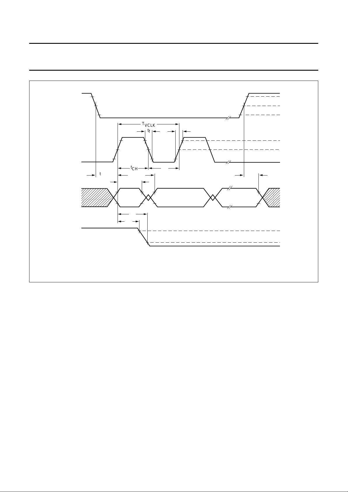
Philips Semiconductors Objective specification
High Performance Scaler (HPS) SAA7140A; SAA7140B
handbook, full pagewidth
VOEN
VCLK
DATA OUTPUT
VRAM port
OUTPUT HFL
not valid
t
enVRO
t
t
ohVRO
t
t
oh
t
CH
odVRO
od
T
VCLK
2.4 V
1.5 V
0.6 V
t
f
t
CL
t
r
2.4 V
1.5 V
0.6 V
t
odVRO
0.85V
DD
0.4 V
0.85V
DD
0.4 V
MHA125
Fig.19 Data output timing (VRAM port).
1996 Sep 04 61
Page 62
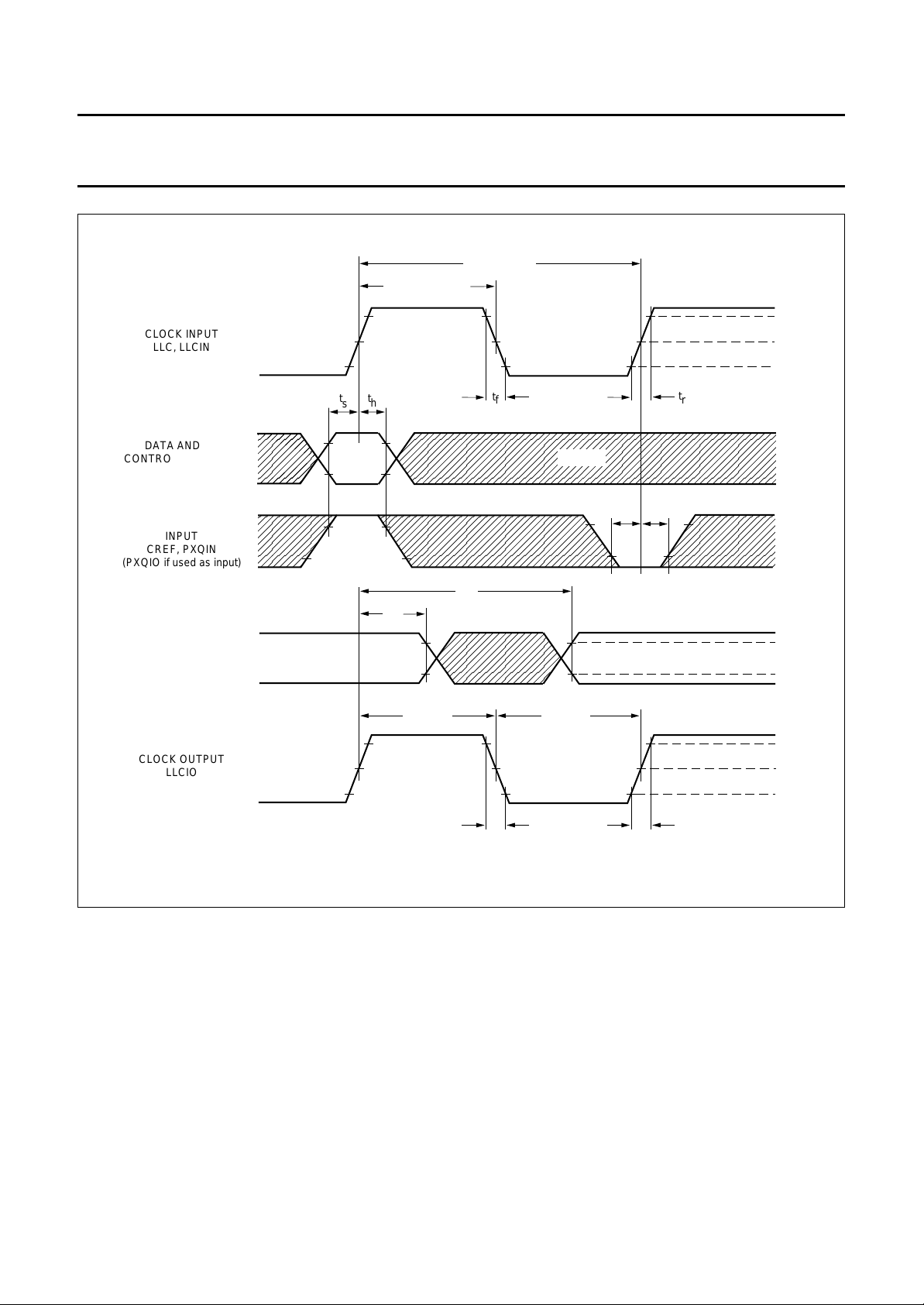
Philips Semiconductors Objective specification
High Performance Scaler (HPS) SAA7140A; SAA7140B
T
handbook, full pagewidth
CLOCK INPUT
LLC, LLCIN
t
LLCH
, t
LLCINH
LLC
, T
LLCIN
2.4 V
1.5 V
0.6 V
DATA AND
CONTROL INPUTS
(DMSD/EXPANSION PORT)
INPUT
CREF, PXQIN
(PXQIO if used as input)
DATA AND
CONTROL OUTPUTS
EXPANSION PORT
CLOCK OUTPUT
LLCIO
t
t
h
s
t
oh
t
LLCIOH
t
f
not valid
t
s
t
od
t
LLCIOL
t
f
t
r
2.4 V
0.6 V
t
h
t
r
2.4 V
0.6 V
0.85V
0.4 V
0.85V
1.5 V
0.4 V
MHA124
DD
DD
Fig.20 Data input/output timing (DMSD port and expansion port).
1996 Sep 04 62
Page 63
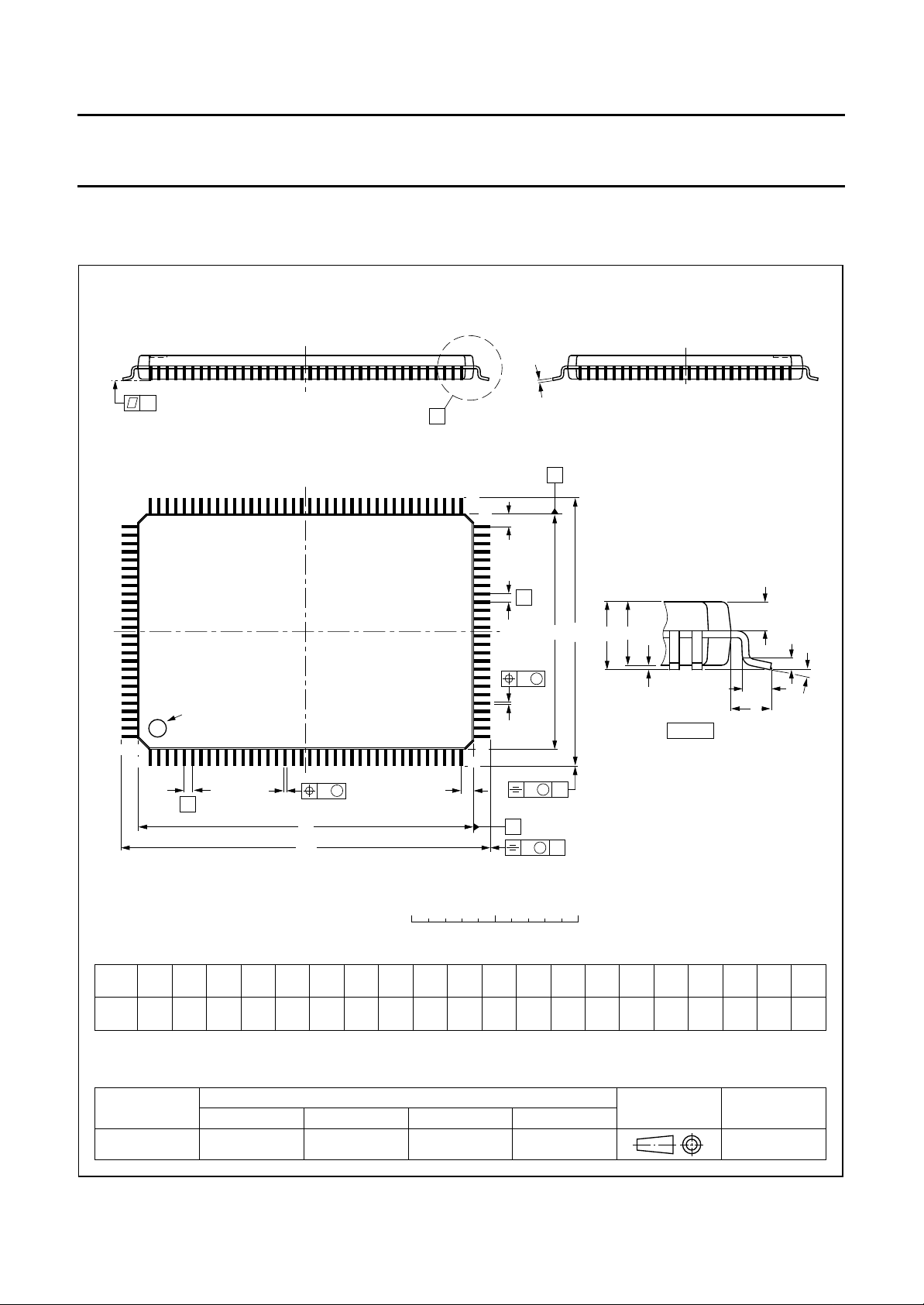
Philips Semiconductors Objective specification
High Performance Scaler (HPS) SAA7140A; SAA7140B
14 PACKAGE OUTLINE
LQFP128: plastic low profile quad flat package; 128 leads; body 14 x 20 x 1.4 mm
c
103
128
y
102
pin 1 index
1
X
A
65
64
Z
E
e
H
E
w M
b
p
39
38
A
A
E
SOT425-1
Q
2
A
1
detail X
(A )
3
L
p
L
θ
w M
b
e
DIMENSIONS (mm are the original dimensions)
mm
OUTLINE
VERSION
SOT425-1
A
max.
1.6
0.15
0.05
1.45
1.35
UNIT A1A2A3bpcE
Note
1. Plastic or metal protrusions of 0.25 mm maximum per side are not included.
p
D
H
D
(1) (1)(1)
D
0.27
0.20
0.25
0.17
IEC JEDEC EIAJ
0.09
20.1
19.9
REFERENCES
Z
D
0 5 10 mm
(1)
eH
H
14.1
13.9
0.5
22.15
21.85
1996 Sep 04 63
D
v M
A
B
v M
B
scale
LLpQZywv θ
E
16.15
15.85
0.75
0.45
0.70
0.58
0.120.2 0.11.0
EUROPEAN
PROJECTION
Z
D
0.81
0.81
0.59
0.59
ISSUE DATE
96-04-02
E
o
7
o
0
Page 64

Philips Semiconductors Objective specification
High Performance Scaler (HPS) SAA7140A; SAA7140B
15 SOLDERING
15.1 Introduction
There is no soldering method that is ideal for all IC
packages. Wave soldering is often preferred when
through-hole and surface mounted components are mixed
on one printed-circuit board. However, wave soldering is
not always suitable for surface mounted ICs, or for
printed-circuits with high population densities. In these
situations reflow soldering is often used.
This text gives a very brief insight to a complex technology.
A more in-depth account of soldering ICs can be found in
our
“IC Package Databook”
15.2 Reflow soldering
Reflow soldering techniques are suitable for all QFP and
SO packages.
The choice of heating method may be influenced by larger
plastic QFP packages (44 leads, or more). If infrared or
vapour phase heating is used and the large packages are
not absolutely dry (less than 0.1% moisture content by
weight), vaporization of the small amount of moisture in
them can cause cracking of the plastic body. For more
information, refer to the Drypack chapter in our
Reference Manual”
Reflow soldering requires solder paste (a suspension of
fine solder particles, flux and binding agent) to be applied
to the printed-circuit board by screen printing, stencilling or
pressure-syringe dispensing before package placement.
Several techniques exist for reflowing; for example,
thermal conduction by heated belt. Dwell times vary
between 50 and 300 seconds depending on heating
method. Typical reflow temperatures range from
215 to 250 °C.
Preheating is necessary to dry the paste and evaporate
the binding agent. Preheating duration: 45 minutes at
45 °C.
(order code 9398 510 63011).
(order code 9398 652 90011).
“Quality
If wave soldering cannot be avoided, the following
conditions must be observed:
• A double-wave (a turbulent wave with high upward
pressure followed by a smooth laminar wave)
soldering technique should be used.
• The footprint must be at an angle of 45° to the board
direction and must incorporate solder thieves
downstream and at the side corners.
Even with these conditions, do not consider wave
soldering the following packages: QFP52 (SOT379-1),
QFP100 (SOT317-1), QFP100 (SOT317-2),
QFP100 (SOT382-1) or QFP160 (SOT322-1).
15.3.2 SO
Wave soldering techniques can be used for all SO
packages if the following conditions are observed:
• A double-wave (a turbulent wave with high upward
pressure followed by a smooth laminar wave) soldering
technique should be used.
• The longitudinal axis of the package footprint must be
parallel to the solder flow.
• The package footprint must incorporate solder thieves at
the downstream end.
15.3.3 M
During placement and before soldering, the package must
be fixed with a droplet of adhesive. The adhesive can be
applied by screen printing, pin transfer or syringe
dispensing. The package can be soldered after the
adhesive is cured.
Maximum permissible solder temperature is 260 °C, and
maximum duration of package immersion in solder is
10 seconds, if cooled to less than 150 °C within
6 seconds. Typical dwell time is 4 seconds at 250 °C.
A mildly-activated flux will eliminate the need for removal
of corrosive residues in most applications.
ETHOD (QFP AND SO)
15.3 Wave soldering
15.3.1 QFP
Wave soldering is not recommended for QFP packages.
This is because of the likelihood of solder bridging due to
closely-spaced leads and the possibility of incomplete
solder penetration in multi-lead devices.
1996 Sep 04 64
15.4 Repairing soldered joints
Fix the component by first soldering two diagonallyopposite end leads. Use only a low voltage soldering iron
(less than 24 V) applied to the flat part of the lead. Contact
time must be limited to 10 seconds at up to 300 °C. When
using a dedicated tool, all other leads can be soldered in
one operation within 2 to 5 seconds between
270 and 320 °C.
Page 65
Philips Semiconductors Objective specification
High Performance Scaler (HPS) SAA7140A; SAA7140B
16 DEFINITIONS
Data sheet status
Objective specification This data sheet contains target or goal specifications for product development.
Preliminary specification This data sheet contains preliminary data; supplementary data may be published later.
Product specification This data sheet contains final product specifications.
Limiting values
Limiting values given are in accordance with the Absolute Maximum Rating System (IEC 134). Stress above one or
more of the limiting values may cause permanent damage to the device. These are stress ratings only and operation
of the device at these or at any other conditions above those given in the Characteristics sections of the specification
is not implied. Exposure to limiting values for extended periods may affect device reliability.
Application information
Where application information is given, it is advisory and does not form part of the specification.
17 LIFE SUPPORT APPLICATIONS
These products are not designed for use in life support appliances, devices, or systems where malfunction of these
products can reasonably be expected to result in personal injury. Philips customers using or selling these products for
use in such applications do so at their own risk and agree to fully indemnify Philips for any damages resulting from such
improper use or sale.
18 PURCHASE OF PHILIPS I
Purchase of Philips I
components in the I2C system provided the system conforms to the I2C specification defined by
Philips. This specification can be ordered using the code 9398 393 40011.
2
C COMPONENTS
2
C components conveys a license under the Philips’ I2C patent to use the
1996 Sep 04 65
Page 66

Philips Semiconductors Objective specification
High Performance Scaler (HPS) SAA7140A; SAA7140B
NOTES
1996 Sep 04 66
Page 67

Philips Semiconductors Objective specification
High Performance Scaler (HPS) SAA7140A; SAA7140B
NOTES
1996 Sep 04 67
Page 68

Philips Semiconductors – a worldwide company
Argentina: see South America
Australia: 34 Waterloo Road, NORTH RYDE, NSW 2113,
Tel. +61 2 9805 4455, Fax. +61 2 9805 4466
Austria: Computerstr. 6, A-1101 WIEN, P.O. Box 213,
Tel. +43 1 60 101, Fax. +43 1 60 101 1210
Belarus: Hotel Minsk Business Center, Bld. 3, r. 1211, Volodarski Str. 6,
220050 MINSK, Tel. +375 172 200 733, Fax. +375 172 200 773
Belgium: see The Netherlands
Brazil: see South America
Bulgaria: Philips Bulgaria Ltd., Energoproject, 15th floor,
51 James Bourchier Blvd., 1407 SOFIA,
Tel. +359 2 689 211, Fax. +359 2 689 102
Canada: PHILIPS SEMICONDUCTORS/COMPONENTS,
Tel. +1 800 234 7381
China/Hong Kong: 501 Hong Kong Industrial Technology Centre,
72 Tat Chee Avenue, Kowloon Tong, HONG KONG,
Tel. +852 2319 7888, Fax. +852 2319 7700
Colombia: see South America
Czech Republic: see Austria
Denmark: Prags Boulevard 80, PB 1919, DK-2300 COPENHAGEN S,
Tel. +45 32 88 2636, Fax. +45 31 57 1949
Finland: Sinikalliontie 3, FIN-02630 ESPOO,
Tel. +358 615 800, Fax. +358 615 80920
France: 4 Rue du Port-aux-Vins, BP317, 92156 SURESNES Cedex,
Tel. +33 1 40 99 6161, Fax. +33 1 40 99 6427
Germany: Hammerbrookstraße 69, D-20097 HAMBURG,
Tel. +49 40 23 53 60, Fax. +49 40 23 536 300
Greece: No. 15, 25th March Street, GR 17778 TAVROS,
Tel. +30 1 4894 339/911, Fax. +30 1 4814 240
Hungary: see Austria
India: Philips INDIA Ltd, Shivsagar Estate, A Block, Dr. Annie Besant Rd.
Worli, MUMBAI 400 018, Tel. +91 22 4938 541, Fax. +91 22 4938 722
Indonesia: see Singapore
Ireland: Newstead, Clonskeagh, DUBLIN 14,
Tel. +353 1 7640 000, Fax. +353 1 7640 200
Israel: RAPAC Electronics, 7 Kehilat Saloniki St, TEL AVIV 61180,
Tel. +972 3 645 0444, Fax. +972 3 649 1007
Italy: PHILIPS SEMICONDUCTORS, Piazza IV Novembre 3,
20124 MILANO, Tel. +39 2 6752 2531, Fax. +39 2 6752 2557
Japan: Philips Bldg 13-37, Kohnan 2-chome, Minato-ku, TOKYO 108,
Tel. +81 3 3740 5130, Fax. +81 3 3740 5077
Korea: Philips House, 260-199 Itaewon-dong, Yongsan-ku, SEOUL,
Tel. +82 2 709 1412, Fax. +82 2 709 1415
Malaysia: No. 76 Jalan Universiti, 46200 PETALING JAYA, SELANGOR,
Tel. +60 3 750 5214, Fax. +60 3 757 4880
Mexico: 5900 Gateway East, Suite 200, EL PASO, TEXAS 79905,
Tel. +9-5 800 234 7381
Middle East: see Italy
Netherlands: Postbus 90050, 5600 PB EINDHOVEN, Bldg. VB,
Tel. +31 40 27 82785, Fax. +31 40 27 88399
New Zealand: 2 Wagener Place, C.P.O. Box 1041, AUCKLAND,
Tel. +64 9 849 4160, Fax. +64 9 849 7811
Norway: Box 1, Manglerud 0612, OSLO,
Tel. +47 22 74 8000, Fax. +47 22 74 8341
Philippines: Philips Semiconductors Philippines Inc.,
106 Valero St. Salcedo Village, P.O. Box 2108 MCC, MAKATI,
Metro MANILA, Tel. +63 2 816 6380, Fax. +63 2 817 3474
Poland: Ul. Lukiska 10, PL 04-123 WARSZAWA,
Tel. +48 22 612 2831, Fax. +48 22 612 2327
Portugal: see Spain
Romania: see Italy
Russia: Philips Russia, Ul. Usatcheva 35A, 119048 MOSCOW,
Tel. +7 095 926 5361, Fax. +7 095 564 8323
Singapore: Lorong 1, Toa Payoh, SINGAPORE 1231,
Tel. +65 350 2538, Fax. +65 251 6500
Slovakia: see Austria
Slovenia: see Italy
South Africa: S.A. PHILIPS Pty Ltd., 195-215 Main Road Martindale,
2092 JOHANNESBURG, P.O. Box 7430 Johannesburg 2000,
Tel. +27 11 470 5911, Fax. +27 11 470 5494
South America: Rua do Rocio 220, 5th floor, Suite 51,
04552-903 São Paulo, SÃO PAULO - SP, Brazil,
Tel. +55 11 821 2333, Fax. +55 11 829 1849
Spain: Balmes 22, 08007 BARCELONA,
Tel. +34 3 301 6312, Fax. +34 3 301 4107
Sweden: Kottbygatan 7, Akalla, S-16485 STOCKHOLM,
Tel. +46 8 632 2000, Fax. +46 8 632 2745
Switzerland: Allmendstrasse 140, CH-8027 ZÜRICH,
Tel. +41 1 488 2686, Fax. +41 1 481 7730
Taiwan: PHILIPS TAIWAN Ltd., 23-30F, 66,
Chung Hsiao West Road, Sec. 1, P.O. Box 22978,
TAIPEI 100, Tel. +886 2 382 4443, Fax. +886 2 382 4444
Thailand: PHILIPS ELECTRONICS (THAILAND) Ltd.,
209/2 Sanpavuth-Bangna Road Prakanong, BANGKOK 10260,
Tel. +66 2 745 4090, Fax. +66 2 398 0793
Turkey: Talatpasa Cad. No. 5, 80640 GÜLTEPE/ISTANBUL,
Tel. +90 212 279 2770, Fax. +90 212 282 6707
Ukraine: PHILIPS UKRAINE, 4 Patrice Lumumba str., Building B, Floor 7,
252042 KIEV, Tel. +380 44 264 2776, Fax. +380 44 268 0461
United Kingdom: Philips Semiconductors Ltd., 276 Bath Road, Hayes,
MIDDLESEX UB3 5BX, Tel. +44 181 730 5000, Fax. +44 181 754 8421
United States: 811 East Arques Avenue, SUNNYVALE, CA 94088-3409,
Tel. +1 800 234 7381
Uruguay: see South America
Vietnam: see Singapore
Yugoslavia: PHILIPS, Trg N. Pasica 5/v, 11000 BEOGRAD,
Tel. +381 11 825 344, Fax.+381 11 635 777
For all other countries apply to: Philips Semiconductors, Marketing & Sales Communications,
Building BE-p, P.O. Box 218, 5600 MD EINDHOVEN, The Netherlands, Fax. +31 40 27 24825
© Philips Electronics N.V. 1996 SCA51
All rights are reserved. Reproduction in whole or in part is prohibited without the prior written consent of the copyright owner.
The information presented in this document does not form part of any quotation or contract, is believed to be accurate and reliable and may be changed
without notice. No liability will be accepted by the publisher for any consequence of its use. Publication thereof does not convey nor imply any license
under patent- or other industrial or intellectual property rights.
Internet: http://www.semiconductors.philips.com
Printed in The Netherlands 657021/1200/02/pp68 Date of release: 1996 Sep 04 Document order number: 9397 750 01068
 Loading...