

Page 1

INTEGRATED CIRCUITS
DATA SH EET
SAA7128H; SAA7129H
Digital video encoder
Product specification
File under Integrated Circuits, IC22
2000 Mar 08
Page 2

Philips Semiconductors Product specification
Digital video encoder SAA7128H; SAA7129H
CONTENTS
1 FEATURES
2 GENERAL DESCRIPTION
3 ORDERING INFORMATION
4 QUICK REFERENCE DATA
5 BLOCK DIAGRAM
6 PINNING
7 FUNCTIONAL DESCRIPTION
7.1 Versatile fader
7.2 Data manager
7.3 Encoder
7.4 RGB processor
7.5 SECAM processor
7.6 Output interface/DACs
7.7 Synchronization
7.8 Clock
7.9 I2C-bus interface
7.10 Input levels and formats
7.11 Bit allocation map
7.12 I2C-bus format
7.13 Slave receiver
7.14 Slave transmitter
8 CHARACTERISTICS
8.1 Explanation of RTCI data bits
8.2 Teletext timing
9 APPLICATION INFORMATION
9.1 Analog output voltages
10 PACKAGE OUTLINE
11 SOLDERING
11.1 Introduction to soldering surface mount
packages
11.2 Reflow soldering
11.3 Wave soldering
11.4 Manual soldering
11.5 Suitability of surface mount IC packages for
wave and reflow soldering methods
12 DEFINITIONS
13 LIFE SUPPORT APPLICATIONS
14 PURCHASE OF PHILIPS I2C COMPONENTS
2000 Mar 08 2
Page 3

Philips Semiconductors Product specification
Digital video encoder SAA7128H; SAA7129H
1 FEATURES
• Monolithic CMOS 3.3 V device, 5 V I2C-bus optional
• Digital PAL/NTSC/SECAM encoder
• System pixel frequency 13.5 MHz
• 54 MHz double-speedmultiplexed D1 interface capable
of splitting data into two separate channels (encoded
and baseband)
• Three Digital-to-Analog Converters (DACs) for CVBS
(CSYNC), VBS (CVBS) and C (CVBS) two times
oversampled with 10-bit resolution (signals in brackets
optional)
• Three DACs for RED (CR), GREEN (Y) and BLUE (CB)
two times oversampled with 9-bit resolution (signals in
brackets optional)
• Alternatively, an advanced composite sync is available
on the CVBS output for RGB display centring
• Real-time control of subcarrier
• Cross-colour reduction filter
• Closed captioning encoding and World Standard
Teletext (WST) and North-American Broadcast Text
System(NABTS) teletextencoding includingsequencer
and filter
• Copy Generation Management System (CGMS)
encoding (CGMS described by standard CPR-1204 of
EIAJ); 20 bits in lines 20/283 (NTSC) can be loaded via
I2C-bus
• Fast I2C-bus control port (400 kHz)
• Line 23 Wide Screen Signalling (WSS) encoding
• Video Programming System (VPS) data encoding in
line 16 (50/625 lines counting)
• Encoder can be master or slave
• Programmable horizontal and vertical input
synchronization phase
• Programmable horizontal sync output phase
• Internal Colour Bar Generator (CBG)
• Macrovision Pay-per-View copy protection system
rev. 7.01 and rev. 6.1 as option; this applies to
SAA7128H only. The deviceis protectedby USA patent
numbers 4631603, 4577216 and 4819098 and other
intellectual property rights. Use of the macrovision
anti-copy process in the device is licensed for
non-commercialhome use only. Reverseengineeringor
disassembly is prohibited. Please contact your nearest
PhilipsSemiconductors salesoffice formore information
• Controlled rise/fall times of output syncs and blanking
• On-chip crystal oscillator (3rd-harmonic or fundamental
crystal)
• Downmode (lowoutput voltage) orpower-save modeof
DACs
• QFP44 package.
2 GENERAL DESCRIPTION
The SAA7128H; SAA7129H encodes digital CB-Y-C
video data to an NTSC, PAL or SECAM CVBS or S-video
signal. Simultaneously, RGB orbypassed butinterpolated
CB-Y-CR signals are available via three additional DACs.
The circuit at a 54 MHz multiplexed digital D1 input port
accepts two ITU-R BT.656 compatible CB-Y-CR data
streams with 720 active pixels per line in
4:2:2multiplexed formats, for example MPEG decoded
data with overlay and MPEG decoded data without
overlay, whereas one data stream is latched at the rising,
the other one at the falling clock edge.
It includes a sync/clock generator and on-chip DACs.
R
3 ORDERING INFORMATION
TYPE NUMBER
SAA7128H QFP44 plastic quad flat package; 44 leads (lead length 1.3 mm); body
SAA7129H
2000 Mar 08 3
NAME DESCRIPTION VERSION
10 × 10 × 1.75 mm
PACKAGE
SOT307-2
Page 4

Philips Semiconductors Product specification
Digital video encoder SAA7128H; SAA7129H
4 QUICK REFERENCE DATA
SYMBOL PARAMETER MIN. TYP. MAX. UNIT
V
V
I
DDA
I
DDD
V
V
R
LE
LE
T
DDA
DDD
i
o(p-p)
L
lf(i)
lf(d)
amb
analog supply voltage 3.15 3.3 3.45 V
digital supply voltage 3.0 3.3 3.6 V
analog supply current − 130 150 mA
digital supply current − 75 100 mA
input signal voltage levels TTL compatible
analog output signal voltages Y, C and CVBS without load
1.25 1.35 1.50 V
(peak-to-peak value)
load resistance 75 − 300 Ω
low frequency integral linearity error −−±3 LSB
low frequency differential linearity error −−±1 LSB
ambient temperature 0 − 70 °C
2000 Mar 08 4
Page 5
This text is here in white to force landscape pages to be rotated correctly when browsing through the pdf in the Acrobat reader.This text is here in
f
_white to force landscape pages to be rotated correctly when browsing through the pdf in the Acrobat reader.This text is here inThis text is here in
white to force landscape pages tobe rotated correctly when browsing through the pdf in the Acrobat reader. white to force landscape pages to be ...
2000 Mar 08 5
ull pagewidth
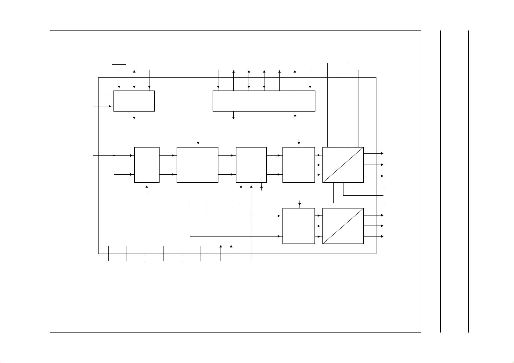
5 BLOCK DIAGRAM
Philips Semiconductors Product specification
Digital video encoder SAA7128H; SAA7129H
V
DD(I2C)
SA
MP7 to MP0
TTX
20
21
9 to 16
44
RESET
40
2
I
MP
MP
SDA
42
I2C-BUS
INTERFACE
C-bus control
pos
SWITCH
neg
I2C-bus control
SCL
DDA1
25
V
DDA2
V
28
DDA3
31
V
DDA4
36
XTALI
XTALO7RCV18RCV243TTXRQ37XCLK4LLC1
41
SAA7128H
35
34
SYNC/CLOCK
V
SAA7129H
MP
MP
clock and timing
A
MP
B
FADER
VP
Y
ENCODER
CbCr
I2C-bus
control
Y
C
Y
CbCr
I2C-bus control
I2C-bus controlI2C-bus control
OUTPUT
INTERFACE
I2C-bus control
RGB
PROCESSOR
30
D
A
D
A
CVBS
(CSYNC)
27
VBS
(CVBS)
24
C
(CVBS)
22
V
32
33
23
26
29
SSA1
V
SSA2
V
SSA3
RED
GREEN
BLUE
V
SSD1
3
V
DDD3
39
V
SSD3
38
V
18
SSD2
5
V
DDD1
6
V
DDD2
17
SP
2
AP
19
MHB572
RTCI
Fig.1 Block diagram.
Page 6

Philips Semiconductors Product specification
Digital video encoder SAA7128H; SAA7129H
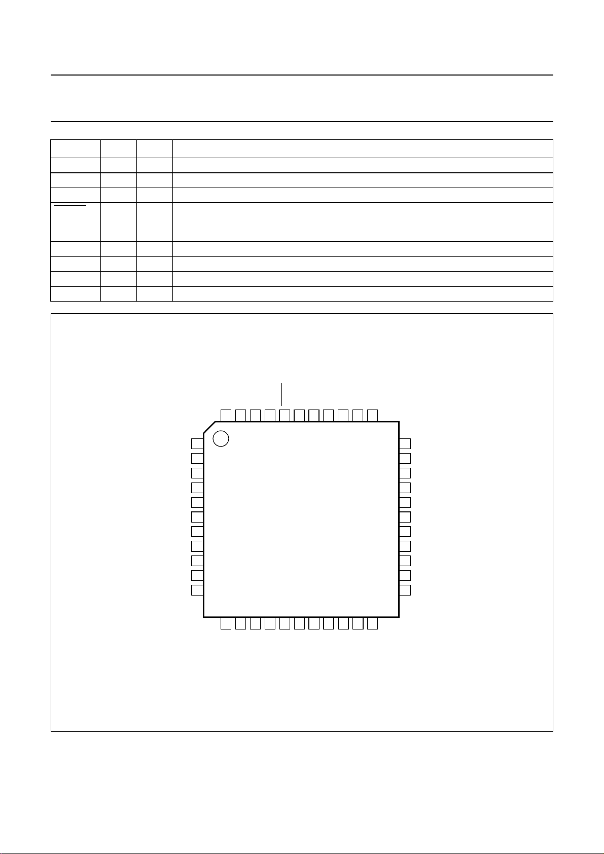
6 PINNING
SYMBOL PIN TYPE DESCRIPTION
RES 1 − reserved pin; do not connect
SP 2 I test pin; connected to digital ground for normal operation
AP 3 I test pin; connected to digital ground for normal operation
LLC1 4 I line-locked clock input; this is the 27 MHz master clock
V
SSD1
V
DDD1
RCV1 7 I/O raster control 1 for video port; this pin receives/provides a VS/FS/FSEQ signal
RCV2 8 I/O raster control 2 for video port; this pin provides an HS pulse of programmable length or
MP7 9 I double-speed 54 MHz MPEG port; it is an input for
MP6 10 I
MP5 11 I
MP4 12 I
MP3 13 I
MP2 14 I
MP1 15 I
MP0 16 I
V
DDD2
V
SSD2
RTCI 19 I real-time control input; if the LLC1 clock is provided by an SAA7111 or SAA7151B, RTCI
V
DD(I2C)
SA 21 I select I
V
SSA1
RED 23 O analog output of RED (C
C 24 O analog output of chrominance (CVBS) signal
V
DDA1
GREEN 26 O analog output of GREEN (Y) signal
VBS 27 O analog output of VBS (CVBS) signal
V
DDA2
BLUE 29 O analog output of BLUE (C
CVBS 30 O analog output of CVBS (CSYNC) signal
V
DDA3
V
SSA2
V
SSA3
XTALO 34 O crystal oscillator output
XTALI 35 I crystal oscillator input; if the oscillator is not used, this pin should be connected to ground
V
DDA4
5 supply digital ground 1
6 supply digital supply voltage 1
receives an HS pulse
“ITU-R BT.656”
style multiplexed
CB-Y-CR data; data is sampled on the rising and falling clock edge; data sampled on the
rising edge is then sent to the encoding part of the device; data sampled on the falling
edge is sent to the RGB part of the device (or vice versa, depending on programming)
17 supply digital supply voltage 2
18 supply digital ground 2
should be connected to the RTCO pin of the respective decoder to improve the signal
quality
20 supply sense input for I2C-bus voltage; connect to I2C-bus supply
2
C-bus address; LOW selects slave address 88H, HIGH selects slave address
8CH
22 supply analog ground 1 for RED (CR), C (CVBS) and GREEN (Y) outputs
) signal
R
25 supply analog supply voltage 1 for RED (CR) and C (CVBS) outputs
28 supply analog supply voltage 2 for VBS (CVBS) and GREEN (Y) outputs
) signal
B
31 supply analog supply voltage 3 for BLUE (CB) and CVBS (CSYNC) outputs
32 supply analog ground 2 for VBS (CVBS), BLUE (CB) and CVBS (CSYNC) outputs
33 supply analog ground 3 for the DAC reference ladder and the oscillator
36 supply analog supply voltage 4 for the DAC reference ladder and the oscillator
2000 Mar 08 6
Page 7
Philips Semiconductors Product specification
Digital video encoder SAA7128H; SAA7129H
SYMBOL PIN TYPE DESCRIPTION
XCLK 37 O clock output of the crystal oscillator
V
SSD3
V
DDD3
RESET 40 I Reset input, active LOW. After reset is applied, all digital I/Os are in input mode; PAL
SCL 41 I I
SDA 42 I/O I
TTXRQ 43 O teletext request output, indicating when text bits are requested
TTX 44 I teletext bit stream input
38 supply digital ground 3
39 supply digital supply voltage 3
black burst on CVBS, VBS and C; RGB outputs set to lowest voltage. The I2C-bus
receiver waits for the START condition.
2
C-bus serial clock input
2
C-bus serial data input/output
handbook, full pagewidth
LLC1
V
SSD1
V
DDD1
RCV1
RCV2
RES
SP
AP
MP7
MP6
MP5
SDA
TTXRQ
43
42
13
14
MP2
MP3
SCL
41
15
TTX
44
1
2
3
4
5
6
7
8
9
10
11
12
MP4
RESET
40
SAA7128H
SAA7129H
16
MP1
MP0
DDD3
V
39
17
DDD2
V
V
38
18
SSD2
V
XCLK
37
19
RTCI
V
XTALI
36
35
21
20
SA
DD(I2C)
V
XTALO
34
22
SSA1
V
V
33
V
32
V
31
30
CVBS
BLUE
29
V
28
VBS
27
GREEN
26
V
25
24
C
RED
23
MHB573
SSA3
SSA2
DDA3
DDA2
DDA1
DDA4
SSD3
Fig.2 Pin configuration.
2000 Mar 08 7
Page 8

Philips Semiconductors Product specification
Digital video encoder SAA7128H; SAA7129H
7 FUNCTIONAL DESCRIPTION
The digital video encoder encodes digital luminance and
colour difference signals into analog CVBS, S-video and
simultaneously RGB or CR-Y-CB signals. NTSC-M, PAL
B/G, SECAM and sub-standards are supported.
Both interlaced and non-interlaced operation is possible
for all standards.
The basic encoder function consists of subcarrier
generation and colour modulation and insertion of
synchronization signals. Luminance and chrominance
signals are filtered in accordance with the standard
requirements of
“RS-170-A”
and
“ITU-R BT.470-3”
.
For ease of analog post filtering the signals are twice
oversampled with respect to the pixel clock before
digital-to-analog conversion.
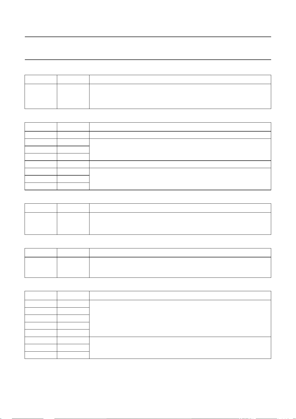
The total filter transfer characteristics are illustrated in
Figs 8 to 13. The DACs for Y, C and CVBS are realized
with full 10-bit resolution; 9-bit resolution for RGB output.
TheCR-Y-CBtoRGB dematrixcan be bypassed optionally
in order to provide the upsampled CR-Y-CB input signals.
The8-bit multiplexed CB-Y-CRformatsare
“ITU-R BT.656”
(D1 format) compatible, but the SAV and EAV codes can
be decoded optionally, when the device is operated in
slave mode. Two independent data streams can be
processed, one latched by the rising edge of LLC1, the
other latched by the falling edge of LLC1. The purpose of
that is e.g. to forward one of the data streams containing
both video and On-Screen Display (OSD) information to
the RGB outputs, and the other stream containing video
only to the encoded outputs CVBS and S-video.
For optimum display of RGB signals through a
euro-connector TV set, optionally on the CVBS output an
early composite sync pulse (up to 31 LLC1 clock periods)
can be provided.
As a further alternative, the VBS and C outputs may
provide a second and third CVBS signal.
Wide screen signalling data can be loadedvia the I2C-bus
and is inserted into line 23 for standards using 50 Hz field
rate.
VPS data for program dependent automatic startand stop
of such featured VCR’s is loadable via I2C-bus.
The IC also contains closed caption and extended data
services encoding (line 21), and supports anti-taping
signalgeneration in accordancewithmacrovision.It is also
possible to load data for copy generation management
system into line 20 of every field (525/60 line counting).
A number of possibilities are provided for setting different
video parameters such as:
• Black and blanking level control
• Colour subcarrier frequency
• Variable burst amplitude etc.
During reset (RESET = LOW) and after reset is released,
all digital I/O stages are set to input mode and the encoder
is set to PAL mode and outputs a ‘black burst’ signal on
CVBS and S-video outputs, while RGB outputs are set to
their lowest output voltages. A reset forces the I2C-bus
interface to abort any running bus transfer.
7.1 Versatile fader Important note: whenever the fader is activated with the
SYMP bit set to a logic 1 (enabling the detection of
embedded Start of Active Video (SAV) and End of Active
Video (EAV)), codes 00H and FFH are not allowed within
the actual video data (as prescribed by
“ITU-R BT.
656”,
anyway). If SAV (00H) has been detected, the fader
automatically passes 100% of the respective signal until
SAV will be detected.
Within the digital video encoder, two data streams can be
faded against each other; these data streams can be input
to the double speed MPEG port, which is able to separate
two independent 27 MHz data streams MPA and MPB via
a cross switch controlled by EDGE1 and EDGE2.
Itis alsopossible to connecta Philips digitalvideo decoder
(SAA7111, SAA7711A, SAA7112 or SAA7151B) to the
SAA7128H; SAA7129H. Via the RTCI pin, connected to
RTCO of a decoder, information concerning actual
subcarrier, PAL-ID and (with SAA7111 and newer types)
definite subcarrier phase can be inserted.
The device synthesizes all necessary internal signals,
colour subcarrier frequency, and synchronization signals,
from that clock.
2000 Mar 08 8
handbook, halfpage
MP
pos
MP
neg
EDGE1 = 0
EDGE1 = 1
EDGE2 = 0
EDGE2 = 1
Fig.3 Cross switch.
MHB574
MP
MP
A
B
Page 9
Philips Semiconductors Product specification
Digital video encoder SAA7128H; SAA7129H
7.1.1 CONFIGURATION EXAMPLES
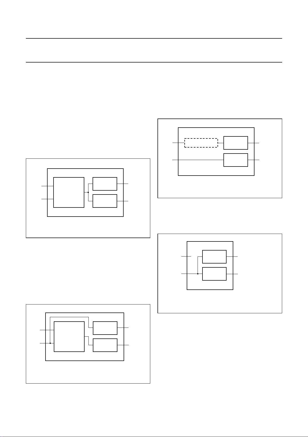
Figs 4 to 7 show examples on how to configure the fader
between the input ports and the outputs, separated into
the composite (and S-video) encoder and the RGB
encoder.
7.1.1.1 Configuration 1
Input MPAcan be faded into MPB. The resulting output of
the fader is then encoded simultaneously to composite
(and S-video) and RGB output (RGBIN = ENCIN = 1).
In this example, either MPA or MPB could be an overlay
(menu) signal to be faded smoothly in and out.
e.g.
video
recorder
e.g. TV
MP
MP
FADER
A
B
MP
OUTPUT
VP
ENCODER
PATH
RGB PATH
MHB575
Fig.4 Configuration 1.
7.1.1.3 Configuration 3
Input MPBis passeddirectly to the RGB output, assuming
e.g.it contains videoincludingoverlay. MPAisequivalently
passed through the inactive fader to the composite (and
S-video) output,assuming e.g. it contains video excluding
overlay (RGBIN = 0, ENCIN = 1).
MP
MP
A
B
FADER BYPASS
ENCODER
PATH
RGB PATH
MHB577
e.g.
video
recorder
e.g. TV
Fig.6 Configuration 3.
7.1.1.4 Configuration 4
OnlyMPBinputis in use;itssignal appears bothcomposite
(and S-video) and RGB encoded (RGBIN = ENCIN = 0).
7.1.1.2 Configuration 2
Input MPAcan be faded into MPB. The resulting output of
the fader is then encoded to RGB output, while the signal
comingfromMPBisfeddirectly to composite(andS-video)
output (RGBIN = 1, ENCIN = 0). Also in this example,
either MPAor MPBcould be anoverlay (menu)signal to be
faded smoothly in and out, whereas the overlay appears
only in the RGB output connected to the TV set.
e.g.
video
recorder
e.g. TV
MP
MP
FADER
A
B
MP
OUTPUT
VP
ENCODER
PATH
RGB PATH
MHB576
Fig.5 Configuration 2.
handbook, halfpage
MP
A
MP
B
ENCODER
PATH
RGB PATH
MHB578
e.g. video recorder
e.g. TV
Fig.7 Configuration 4.
2000 Mar 08 9
Page 10

Philips Semiconductors Product specification
Digital video encoder SAA7128H; SAA7129H
7.1.2 PARAMETERS OF THE FADER
Basically, there are three independent fade factors
available, allowing for the equation:
Output FADEx ln1×()1 FADEx–()ln2×[]+=
Where x = 1, 2 or 3
Factor FADE1 is effective, when a colour in the data
stream fed to the MPEG port fader input is recognized as
being between KEY1L and KEY1U. That means, the
colour is not identified by a single numeric value, but an
upper and lower threshold in a 24-bit YUV colour space
canbe defined. FADE1 = 00Hresultsin100% signal atthe
MPEG port fader input and 0% signal at the fader Video
port input. Variation of 63 steps is possible up to
FADE1 = 3FH, resulting in 0% signal at the MPEG port
fader input and 100% signal at the fader Video port input.
Factor FADE2 is effective, when a colour in the data
stream fed to the MPEG port fader input is recognized as
being between KEY2L and KEY2U. FADE2 is to be seen
in conjunction with a colour that is defined by a 24-bit
internal Colour Look-Up Table (CLUT). FADE2 = 00H
results in 100% of the internally defined LUT colour and
0% signal at the fader Video port input. Variation of
63 stepsis possibleupto FADE2 = 3FH,resulting in0%of
the internally defined LUT colour and 100% signal at the
fader Video port input.
Finally,factor FADE3 iseffective,whena colour inthedata
stream fed to the MPEG port fader input is recognized as
neither being between KEY1L and KEY1U nor being
between KEY2L and KEY2H. FADE3 = 00H results in
100% signal at the MPEG port fader input and 0% signal
at the fader Video port input. Variation of 63 steps is
possible up to FADE3 = 3FH, resulting in 0% signal at the
MPEG port fader input and 100%signal atthe fader Video
port input.
Optionally, all upper and lower thresholds can be ignored,
enabling to fade signals only against the LUT colour.
If bit CFADM is set HIGH, all data at the MPEG port fader
are faded against the LUT colour, if bit CFADV is set
HIGH,all dataatthe Videoportfader arefadedagainst the
LUT colour.
7.3 Encoder
7.3.1 VIDEO PATH
The encoder generates out of Y, U and V baseband
signals luminance and colour subcarrier output signals,
suitable for use as CVBS or separate Y and C signals.
Luminance is modified in gain and in offset (latter
programmable in a certain range to enable different black
level set-ups). After insertion of a fixed synchronization
pulse tip level, in accordance with standard composite
synchronization schemes, a blanking level can be set.
Other manipulations used for the macrovision anti-taping
process like additional insertion of AGC super-white
pulses (programmable in height) are supported by
SAA7128H only.
In order to enable easy analog post filtering, luminance is
interpolated from 13.5 MHz data rate to 27 MHzdata rate,
providing luminance in 10-bit resolution. The transfer
characteristics of the luminance interpolation filter are
illustrated in Figs 10 and 11. Appropriate transients at
start/end of active video and for synchronization pulses
are ensured.
Chrominance is modified in gain (programmable
separately for U and V), standard dependent burst is
inserted, before baseband colour signals are interpolated
from 6.75 MHz data rate to 27 MHz data rate. One of the
interpolation stages can be bypassed, thus providing a
higher colour bandwidth, which can be made use of for
Y and C output. The transfer characteristics of the
chrominance interpolation filter are illustrated in
Figs 8 and 9.
Theamplitude, beginningand ending ofthe insertedburst,
is programmable in a certain range that is suitable for
standard signals and for special effects. Behind the
succeeding quadrature modulator, colour in 10-bit
resolution is provided on subcarrier.
The numeric ratio between Y and C outputs is in
accordance with the respective standards.
7.2 Data manager
In the data manager, alternatively to the external video
data, a pre-defined colour look-up table located in this
block can be read out in a pre-defined sequence (8 steps
per active video line), achieving a colour bar test pattern
generator without the need for an external data source.
2000 Mar 08 10
Page 11

Philips Semiconductors Product specification
Digital video encoder SAA7128H; SAA7129H
7.3.2 TELETEXT INSERTION AND ENCODING
Pin TTX receives a WST or NABTS teletext bitstream
sampled at the LLC clock. Two protocols are provided:
• At each rising edge of output signal (TTXRQ) a single
teletext bit has to be provided after a programmable
delay at input pin TTX
• Thesignal TTXRQ performsonlya single LOW-to-HIGH
transition and remains atHIGH levelfor 360,296 or 288
teletext bits, depending on the chosen standard.
Phase variant interpolationis achievedon thisbitstream in
the internal teletext encoder, providing sufficient small
phase jitter on the output text lines.
TTXRQ provides a fully programmable request signal to
the teletext source, indicating the insertion period of
bitstream at lines which are selectable independently for
both fields. The internal insertion window for text is set to
360 (PAL-WST), 296 (NTSC-WST) or 288 (NABTS)
teletext bits including clock run-in bits. The protocol and
timing are illustrated in Fig.23.
7.3.3 VIDEO PROGRAMMING SYSTEM (VPS) ENCODING
Five bytes of VPS information can be loaded via the
I2C-bus and will be encoded in the appropriate format into
line 16.
7.3.4 CLOSED CAPTION ENCODER
Using this circuit,data inaccordance withthe specification
of closed caption or extended data service, delivered by
the control interface, can be encoded (line 21). Two
dedicated pairs of bytes (two bytes per field), each pair
preceded by run-in clocks and framing code, are possible.
Theactual line numberwheredata is tobeencoded in, can
be modified in a certain range.
The data clock frequency is in accordance with the
definition for NTSC-M standard 32 times horizontal line
frequency.
DataLOW at theoutputof the DACscorresponds to 0 IRE,
data HIGH at the output of the DACs corresponds to
approximately 50 IRE.
It is also possible to encode closed caption data for 50 Hz
field frequencies at 32 times horizontal line frequency.
7.3.5 ANTI-TAPING (SAA7128H ONLY)
For more information contact your nearest Philips
Semiconductors sales office.
7.4 RGB processor
This block contains a dematrix in order to produce red,
green and blue signals to be fed to a SCART plug.
Before Y, CBand CR signals are de-matrixed, individual
gain adjustment for Y and colour difference signals and
2 times oversampling for luminance and 4 times
oversampling for colour difference signals is performed.
The transfer curves of luminance and colour difference
components of RGB are illustrated in Figs 12 and 13.
7.5 SECAM processor
SECAM specific pre-processing is achieved in this block
by a pre-emphasis of colour difference signals (for gain
and phase see Figs 14 and 15).
A baseband frequency modulator with a reference
frequency shifted from 4.286 MHz to DC carries out
SECAM modulation in accordance with appropriate
standard or optionally wide clipping limits.
Afterthe HF pre-emphasis,alsoapplied on aDCreference
carrier (anti-Clochefilter; see Figs 16 and 17),line-by-line
sequential carriers with black reference of 4.25 MHz (Db)
and 4.40625 MHz (Dr) are generated using specified
values for FSC programming bytes.
Alternating phase reset in accordance with SECAM
standard is carried out automatically. During vertical
blanking the so-called bottle pulses are not provided.
7.6 Output interface/DACs
In the output interface, encoded Y and C signals are
converted from digital-to-analog in a 10-bit resolution.
Y and C signals are also combined to a 10-bit CVBS
signal.
The CVBS output occurs with the same processing delay
(equal to 82 LLC clock periods, measured from MP input
to the analog outputs) as the Y, C and RGB outputs.
Absolute amplitude at the input of the DAC for CVBS is
reduced by15⁄16 with respect to Y and C DACs to make
maximum use of conversion ranges.
Red, green and blue signals are also converted from
digital-to-analog, each providing a 9-bit resolution.
Outputs of the DACs can be set together via software
control to minimum output voltage (approximately 0.2 V
DC) for either purpose. Alternatively, the buffers can be
switchedinto 3-state outputcondition;this allowsfor‘wired
AND’ing with other 3-state outputs and can also be used
as a power-save mode.
2000 Mar 08 11
Page 12

Philips Semiconductors Product specification
Digital video encoder SAA7128H; SAA7129H
7.7 Synchronization
The synchronization of theSAA7128H; SAA7129His able
to operate in two modes; slave mode and master mode.
In master mode (see Fig.19), the circuit generates all
necessary timings in the video signal itself, and it can
provide timing signals at the RCV1 and RCV2 ports.
In slavemode, itacceptstiming informationeitherfrom the
RCV pins or from the embedded timing data of the
ITU-R BT.656 data stream.
For the SAA7128H; SAA7129H, the only difference
between master and slave mode is that it ignores the
timing information at its inputs in master mode. Thus, if in
slave mode, any timing information is missing, the IC will
continue running free without a visible effect. But there
must not be any additional pulses (with wrong phase)
because the circuit will not ignore them.
In slave mode (see Fig.18), an interface circuit decides,
which signal is expected at the RCV1 port and which
information is taken from its active slope. The polarity can
be chosen, if PRCV1 is logic 0 the rising slope will be
active.
The signal can be:
• A Vertical Sync (VS) pulse; the active slope sets the
vertical phase
• An odd/even signal; the active slope sets the vertical
phase, the internal field flag to odd and optionally sets
the horizontal phase
• A Field Sequence (FSEQ) signal; it marks the first field
of the 4 (NTSC), 8 (PAL) respectively 12 (SECAM) field
sequence. In additionto theodd/even signal,it also sets
the PAL phase and optionally defines the subcarrier
phase.
In slave mode, the horizontal trigger phase can be
programmed to any point in the line, the vertical phase
from line 0 to line 15 counted from the first serration pulse
in half line steps.
Whenever synchronization information cannot be derived
directly from the inputs, the SAA7128H; SAA7129H will
calculate it from the internal horizontal, vertical and PAL
phase. This gives good flexibility with respect to external
synchronization but the circuit does not suppress illegal
settings. In such an event, e.g the odd/even information
may vanish as it does in the non-interlaced modes.
In master mode, the line lengths are fixed to 1728 clocks
at 50 Hz and 1716 clocks at 60 Hz. To allow
non-interlaced frames, the field lengths can be varied by
±0.5 lines. In the event of non-interlace, the SAA7128H;
SAA7129Hdoes not provideodd/even information andthe
output signal does not contain the PAL ‘Bruch sequence’.
At the RCV1 pin the IC can provide:
• A Vertical Sync(VS) signalwith 2.5 (50 Hz)or 3 (60 Hz)
lines duration
• An odd/even signal which is LOW in odd fields
• A Field Sequence (FSEQ) signal which is HIGH in the
first field of the 4, 8 respectively 12 field sequence.
At the RCV2 pin, there is a horizontal pulse of
programmable phase and duration available. This pulse
can be suppressed in the programmable inactive part of a
field giving a composite blank signal.
The directions and polarities of the RCV ports can be
chosen independently. Timing references can be found in
Tables 52 and 60.
7.8 Clock
On the RCV2 port, the IC can provide a horizontal pulse
withprogrammable startand stop phase;this pulsecan be
inhibited in the vertical blanking period to build up, for
example, a composite blanking signal.
The horizontal phase can be set via a separate input
RCV2. In the event of VS pulses at RCV1, this is
mandatory.It is alsopossible to setthesignal path toblank
via this input.
From the ITU-R BT.656 data stream, the SAA7128H;
SAA7129Hdecodes only thestart of thefirstline in theodd
field. All other information is ignored and may miss. If this
kind of slave mode is active, the RCV pins may be
switched to output mode.
2000 Mar 08 12
The input to LLC1 can either be an external clock source
or the buffered on-chip clock XCLK. The internal crystal
oscillator can be run with either a 3rd-harmonic or a
fundamental crystal.
2
7.9 I
The I2C-bus interface is a standard slave transceiver,
supporting 7-bit slave addresses and 400 kbits/s
guaranteed transfer rate. It uses 8-bit subaddressing with
an auto-increment function. All registers are write and
readable, except one read only status byte.
The I2C-bus slave address is defined as 88H with pin 21
(SA) tied LOW and as 8CH with pin 21 (SA) tied HIGH.
C-bus interface
Page 13
Philips Semiconductors Product specification
Digital video encoder SAA7128H; SAA7129H
7.10 Input levels and formats
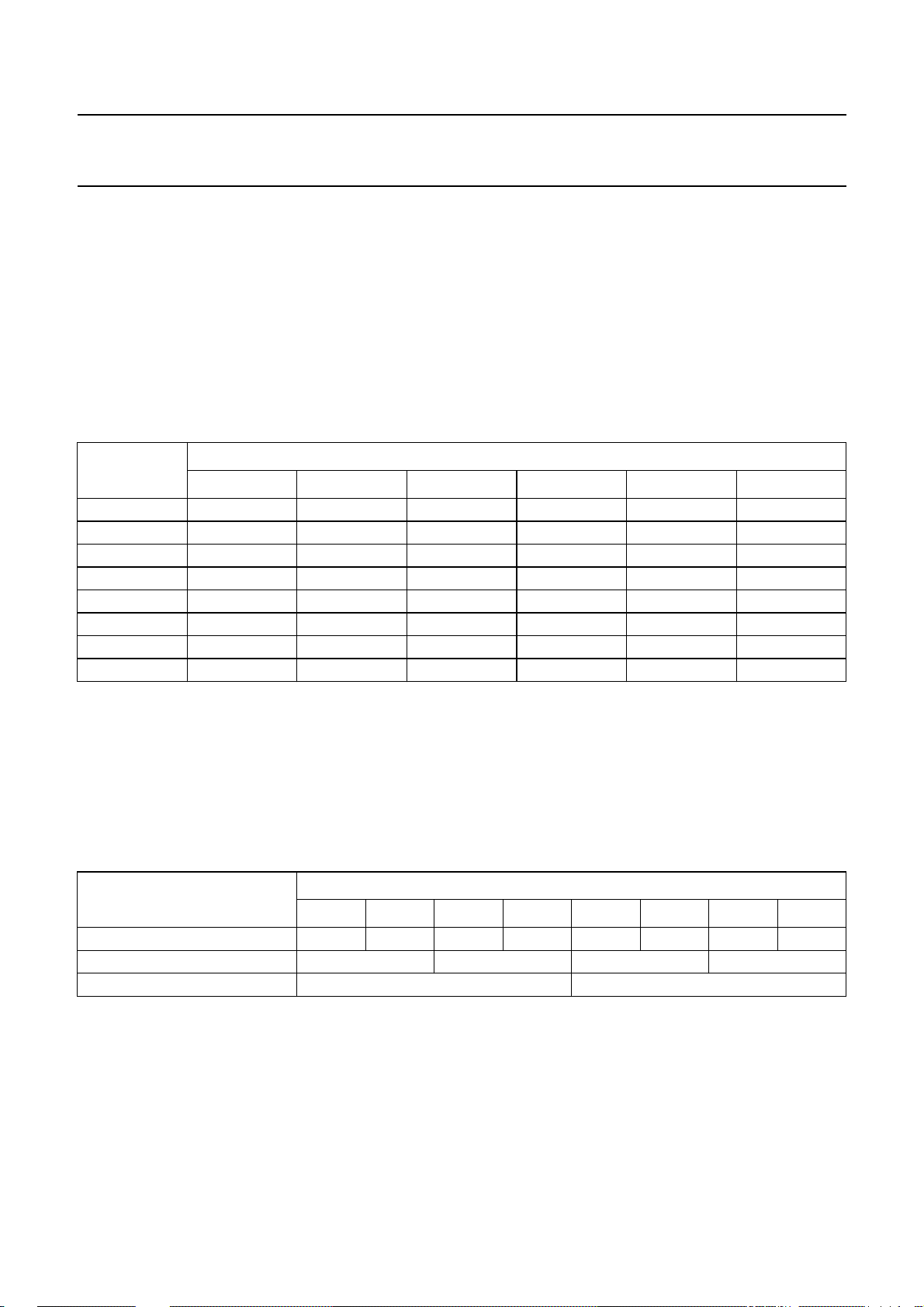
TheSAA7128H; SAA7129H expectsdigitalY, CB,CRdata
with levels (digital codes) in accordance with
“ITU-R BT.601”
.
For C and CVBS outputs, deviating amplitudes of the
The RGB, respectively CR-Y-CB path features a gain
setting individually for luminance (GY) and colour
difference signals (GCD).
Reference levels are measured with a colour bar,
100% white, 100% amplitude and 100% saturation.
colour difference signals can be compensated by
independent gain control setting, while gain for luminance
is set to predefined values, distinguishable for 7.5 IRE
set-up or without set-up.
Table 1
“ITU-R BT.601”
COLOUR
signal component levels
YC
B
SIGNALS
C
R
(1)
(2)
R
(2)
G
B
White 235 128 128 235 235 235
Yellow 210 16 146 235 235 16
Cyan 170 166 16 16 235 235
Green 145 54 34 16 235 16
Magenta 106 202 222 235 16 235
Red 81 90 240 235 16 16
Blue 41 240 110 16 16 235
Black 16 128 128 16 16 16
(2)
Notes
1. Transformation:
a) R = Y + 1.3707 × (CR− 128)
b) G = Y − 0.3365 × (CB− 128) − 0.6982 × (CR− 128)
c) B = Y + 1.7324 × (CB− 128).
2. Representation of R, G and B (or CR, Y and CB) at the output is 9 bits at 27 MHz.
Table 2 8-bit multiplexed format (similar to
“ITU-R BT.601”
)
BITS
TIME
01234567
Sample C
0Y0C
B
0Y1C
R
2Y2C
B
2Y3
R
Luminance pixel number 0123
Colour pixel number 0 2
2000 Mar 08 13
Page 14

2000 Mar 08 14
7.11 Bit allocation map Table 3 Slave receiver (slave address 88H)
REGISTER FUNCTION SUBADDR
Status byte (read only) 00H VER2 VER1 VER0 CCRDO CCRDE 0 FSEQ O_E
Null 01H to 25H 0 0000000
Wide screen signal 26H WSS7 WSS6 WSS5 WSS4 WSS3 WSS2 WSS1 WSS0
Wide screen signal 27H WSSON 0 WSS13 WSS12 WSS11 WSS10 WSS9 WSS8
Real-time control, burst start 28H DECCOL DECFIS BS5 BS4 BS3 BS2 BS1 BS0
Burst end 29H 0 0 BE5 BE4 BE3 BE2 BE1 BE0
Copy generation 0 2AH CG07 CG06 CG05 CG04 CG03 CG02 CG01 CG00
Copy generation 1 2BH CG15 CG14 CG13 CG12 CG11 CG10 CG09 CG08
CG enable, copy generation 2 2CH CGEN 0 0 0 CG19 CG18 CG17 CG16
Output port control 2DH CVBSEN1 CVBSEN0 CVBSTRI YTRI CTRI RTRI GTRI BTRI
Null 2EH to 37H 0 0000000
Gain luminance for RGB 38H 0 0 0 GY4 GY3 GY2 GY1 GY0
Gain colour difference for RGB 39H 0 0 0 GCD4 GCD3 GCD2 GCD1 GCD0
Input port control 1 3AH CBENB 0 0 SYMP DEMOFF CSYNC MP2C VP2C
Key colour 1 lower limit U 42H KEY1LU7 KEY1LU6 KEY1LU5 KEY1LU4 KEY1LU3 KEY1LU2 KEY1LU1 KEY1LU0
Key colour 1 lower limit V 43H KEY1LV7 KEY1LV6 KEY1LV5 KEY1LV4 KEY1LV3 KEY1LV2 KEY1LV1 KEY1LV0
Key colour 1 lower limit Y 44H KEY1LY7 KEY1LY6 KEY1LY5 KEY1LY4 KEY1LY3 KEY1LY2 KEY1LY1 KEY1LY0
Key colour 2 lower limit U 45H KEY2LU7 KEY2LU6 KEY2LU5 KEY2LU4 KEY2LU3 KEY2LU2 KEY2LU1 KEY2LU0
Key colour 2 lower limit V 46H KEY2LV7 KEY2LV6 KEY2LV5 KEY2LV4 KEY2LV3 KEY2LV2 KEY2LV1 KEY2LV0
Key colour 2 lower limit Y 47H KEY2LY7 KEY2LY6 KEY2LY5 KEY2LY4 KEY2LY3 KEY2LY2 KEY2LY1 KEY2LY0
Key colour 1 upper limit U 48H KEY1UU7 KEY1UU6 KEY1UU5 KEY1UU4 KEY1UU3 KEY1UU2 KEY1UU1 KEY1UU0
Key colour 1 upper limit V 49H KEY1UV7 KEY1UV6 KEY1UV5 KEY1UV4 KEY1UV3 KEY1UV2 KEY1UV1 KEY1UV0
Key colour 1 upper limit Y 4AH KEY1UY7 KEY1UY6 KEY1UY5 KEY1UY4 KEY1UY3 KEY1UY2 KEY1UY1 KEY1UY0
Key colour 2 upper limit U 4BH KEY2UU7 KEY2UU6 KEY2UU5 KEY2UU4 KEY2UU3 KEY2UU2 KEY2UU1 KEY2UU0
Key colour 2 upper limit V 4CH KEY2UV7 KEY2UV6 KEY2UV5 KEY2UV4 KEY2UV3 KEY2UV2 KEY2UV1 KEY2UV0
Key colour 2 upper limit Y 4DH KEY2UY7 KEY2UY6 KEY2UY5 KEY2UY4 KEY2UY3 KEY2UY2 KEY2UY1 KEY2UY0
Fade factor key colour 1 4EH 0 0 FADE15 FADE14 FADE13 FADE12 FADE11 FADE10
CFade, Fade factor key
colour 2
4FH CFADEM CFADEV FADE25 FADE24 FADE23 FADE22 FADE21 FADE20
D7 D6 D5 D4 D3 D2 D1 D0
DATA BYTE
(1)
Philips Semiconductors Product specification
Digital video encoder SAA7128H; SAA7129H
Page 15

2000 Mar 08 15
REGISTER FUNCTION SUBADDR
Fade factor other 50H 0 0 FADE35 FADE34 FADE33 FADE32 FADE31 FADE30
Look-up table key colour 2 U 51H LUTU7 LUTU6 LUTU5 LUTU4 LUTU3 LUTU2 LUTU1 LUTU0
Look-up table key colour 2 V 52H LUTV7 LUTV6 LUTV5 LUTV4 LUTV3 LUTV2 LUTV1 LUTV0
Look-up table key colour 2 Y 53H LUTY7 LUTY6 LUTY5 LUTY4 LUTY3 LUTY2 LUTY1 LUTY0
VPS enable, input control 2 54H VPSEN 0 ENCIN RGBIN DELIN VPSEL EDGE2 EDGE1
VPS byte 5 55H VPS57 VPS56 VPS55 VPS54 VPS53 VPS52 VPS51 VPS50
VPS byte 11 56H VPS117 VPS116 VPS115 VPS114 VPS113 VPS112 VPS111 VPS110
VPS byte 12 57H VPS127 VPS126 VPS125 VPS124 VPS123 VPS122 VPS121 VPS120
VPS byte 13 58H VPS137 VPS136 VPS135 VPS134 VPS133 VPS132 VPS131 VPS130
VPS byte 14 59H VPS147 VPS146 VPS145 VPS144 VPS143 VPS142 VPS141 VPS140
Chrominance phase 5AH CHPS7 CHPS6 CHPS5 CHPS4 CHPS3 CHPS2 CHPS1 CHPS0
Gain U 5BH GAINU7 GAINU6 GAINU5 GAINU4 GAINU3 GAINU2 GAINU1 GAINU0
Gain V 5CH GAINV7 GAINV6 GAINV5 GAINV4 GAINV3 GAINV2 GAINV1 GAINV0
Gain U MSB, real-time control,
black level
Gain V MSB,real-time control,
blanking level
CCR, blanking level VBI 5FH CCRS1 CCRS0 BLNVB5 BLNVB4 BLNVB3 BLNVB2 BLNVB1 BLNVB0
Null 60H 0 0000000
Standard control 61H DOWNB DOWNA INPI YGS SECAM SCBW PAL FISE
RTC enable, burst amplitude 62H RTCE BSTA6 BSTA5 BSTA4 BSTA3 BSTA2 BSTA1 BSTA0
Subcarrier 0 63H FSC07 FSC06 FSC05 FSC04 FSC03 FSC02 FSC01 FSC00
Subcarrier 1 64H FSC15 FSC14 FSC13 FSC12 FSC11 FSC10 FSC09 FSC08
Subcarrier 2 65H FSC23 FSC22 FSC21 FSC20 FSC19 FSC18 FSC17 FSC16
Subcarrier 3 66H FSC31 FSC30 FSC29 FSC28 FSC27 FSC26 FSC25 FSC24
Line 21 odd 0 67H L21O07 L21O06 L21O05 L21O04 L21O03 L21O02 L21O01 L21O00
Line 21 odd 1 68H L21O17 L21O16 L21O15 L21O14 L21O13 L21O12 L21O11 L21O10
Line 21 even 0 69H L21E07 L21E06 L21E05 L21E04 L21E03 L21E02 L21E01 L21E00
Line 21 even 1 6AH L21E17 L21E16 L21E15 L21E14 L21E13 L21E12 L21E11 L21E10
RCV port control 6BH SRCV11 SRCV10 TRCV2 ORCV1 PRCV1 CBLF ORCV2 PRCV2
Trigger control 6CH HTRIG7 HTRIG6 HTRIG5 HTRIG4 HTRIG3 HTRIG2 HTRIG1 HTRIG0
5DH GAINU8 DECOE BLCKL5 BLCKL4 BLCKL3 BLCKL2 BLCKL1 BLCKL0
5EH GAINV8 DECPH BLNNL5 BLNNL4 BLNNL3 BLNNL2 BLNNL1 BLNNL0
D7 D6 D5 D4 D3 D2 D1 D0
DATA BYTE
(1)
Philips Semiconductors Product specification
Digital video encoder SAA7128H; SAA7129H
Page 16

2000 Mar 08 16
DATA BYTE
REGISTER FUNCTION SUBADDR
D7 D6 D5 D4 D3 D2 D1 D0
Trigger control 6DH HTRIG10 HTRIG9 HTRIG8 VTRIG4 VTRIG3 VTRIG2 VTRIG1 VTRIG0
Multi control 6EH SBLBN BLCKON PHRES1 PHRES0 LDEL1 LDEL0 FLC1 FLCO
Closed caption, teletext enable 6FH CCEN1 CCEN0 TTXEN SCCLN4 SCCLN3 SCCLN2 SCCLN1 SCCLN0
RCV2 output start 70H RCV2S7 RCV2S6 RCV2S5 RCV2S4 RCV2S3 RCV2S2 RCV2S1 RCV2S0
RCV2 output end 71H RCV2E7 RCV2E6 RCV2E5 RCV2E4 RCV2E3 RCV2E2 RCV2E1 RCV2E0
MSBs RCV2 output 72H 0 RCV2E10 RCV2E9 RCV2E8 0 RCV2S10 RCV2S9 RCV2S8
TTX request H start 73H TTXHS7 TTXHS6 TTXHS5 TTXHS4 TTXHS3 TTXHS2 TTXHS1 TTXHS0
TTX request H delay 74H TTXHD7 TTXHD6 TTXHD5 TTXHD4 TTXHD3 TTXHD2 TTXHD1 TTXHD0
CSYNC advance, Vsync shift 75H CSYNCA4 CSYNCA3 CSYNCA2 CSYNCA1 CSYNCA0 VS_S2 VS_S1 VS_S0
TTX odd request vertical start 76H TTXOVS7 TTXOVS6 TTXOVS5 TTXOVS4 TTXOVS3 TTXOVS2 TTXOVS1 TTXOVS0
TTX odd request vertical end 77H TTXOVE7 TTXOVE6 TTXOVE5 TTXOVE4 TTXOVE3 TTXOVE2 TTXOVE1 TTXOVE0
TTX even request vertical start 78H TTXEVS7 TTXEVS6 TTXEVS5 TTXEVS4 TTXEVS3 TTXEVS2 TTXEVS1 TTXEVS0
TTX even request vertical end 79H TTXEVE7 TTXEVE6 TTXEVE5 TTXEVE4 TTXEVE3 TTXEVE2 TTXEVE1 TTXEVE0
First active line 7AH FAL7 FAL6 FAL5 FAL4 FAL3 FAL2 FAL1 FAL0
Last active line 7BH LAL7 LAL6 LAL5 LAL4 LAL3 LAL2 LAL1 LAL0
TTX mode, MSB vertical 7CH TTX60 LAL8 TTXO FAL8 TTXEVE8 TTXOVE8 TTXEVS8 TTXOVS8
Null 7DH 0 0000000
Disable TTX line 7EH LINE12 LINE11 LINE10 LINE9 LINE8 LINE7 LINE6 LINE5
Disable TTX line 7FH LINE20 LINE19 LINE18 LINE17 LINE16 LINE15 LINE14 LINE13
(1)
Philips Semiconductors Product specification
Digital video encoder SAA7128H; SAA7129H
Note
1. All bits labelled ‘0’ are reserved. They must be programmed with logic 0.
Page 17

Philips Semiconductors Product specification
Digital video encoder SAA7128H; SAA7129H
7.12 I2C-bus format
2
Table 4 I
S SLAVE ADDRESS ACK SUBADDRESS ACK DATA 0 ACK -------- DATA n ACK P
Table 5 Explanation of Table 4
S START condition
SLAVE ADDRESS 1000100X or 1000 110X; note 1
ACK acknowledge, generated by the slave
SUBADDRESS; note 2 subaddress byte
DATA data byte
-------- continued data bytes and ACKs
P STOP condition
Notes
1. X is the read/write control bit; X = logic 0 is order to write; X = logic 1 is order to read.
2. If more than 1 byte DATA is transmitted, then auto-increment of the subaddress is performed.
C-bus address; see Table 5
PART DESCRIPTION
7.13 Slave receiver
Table 6 Subaddress 26H
BIT SYMBOL DESCRIPTION
7 WSS7 Wide screen signalling bits: enhanced services field.
6 WSS6
5 WSS5
4 WSS4
3 WSS3 Wide screen signalling bits: aspect ratio field.
2 WSS2
1 WSS1
0 WSS0
Table 7 Subaddress 27H
BIT SYMBOL DESCRIPTION
7 WSSON 0 = wide screen signalling output is disabled; default state after reset
1 = wide screen signalling output is enabled
6 − This bit is reserved and must be set to logic 0.
5 WSS13 Wide screen signalling bits: reserved field.
4 WSS12
3 WSS11
2 WSS10 Wide screen signalling bits: subtitles field.
1 WSS9
0 WSS8
2000 Mar 08 17
Page 18

Philips Semiconductors Product specification
Digital video encoder SAA7128H; SAA7129H
Table 8 Subaddress 28H
BIT SYMBOL DESCRIPTION
7 DECCOL 0 = disable colour detection bit of RTCI input
1 = enable colour detection bit of RTCI input; bit RTCE must be set to logic 1 (see
Fig.22)
6 DECFIS 0 = field sequence as FISE in subaddress 61
1 = field sequence as FISE bit in RTCI input; bit RTCE must be set to logic 1 (see
Fig.22)
5 BS5 starting point of burst in clock cycles
4 BS4 PAL: BS[5:0] = 33 (21H); default value after reset
3 BS3
2 BS2
1 BS1
0 BS0
Table 9 Subaddress 29H
NTSC: BS[5:0] = 25 (19H)
BIT SYMBOL DESCRIPTION
7 − These 2 bits are reserved; each must be set to logic 0.
6 −
5 BE5 ending point of burst in clock cycles
4 BE4
3 BE3
2 BE2
1 BE1
0 BE0
Table 10 Subaddress 2AH
BIT SYMBOL DESCRIPTION
7 to 0 CG[07:00] LSB of the byte is encoded immediately after run-in, the MSB of the byte has to carry
Table 11 Subaddress 2BH
BIT SYMBOL DESCRIPTION
7 to 0 CG[15:08] Second byte; the MSB of the byte has to carry the CRCC bit, in accordance with the
PAL: BE[5:0] = 29 (1DH); default value after reset
NTSC: BE[5:0] = 29 (1DH)
the CRCC bit, in accordance with the definition of copygeneration management system
encoding format.
definition of copy generation management system encoding format.
2000 Mar 08 18
Page 19
Philips Semiconductors Product specification
Digital video encoder SAA7128H; SAA7129H
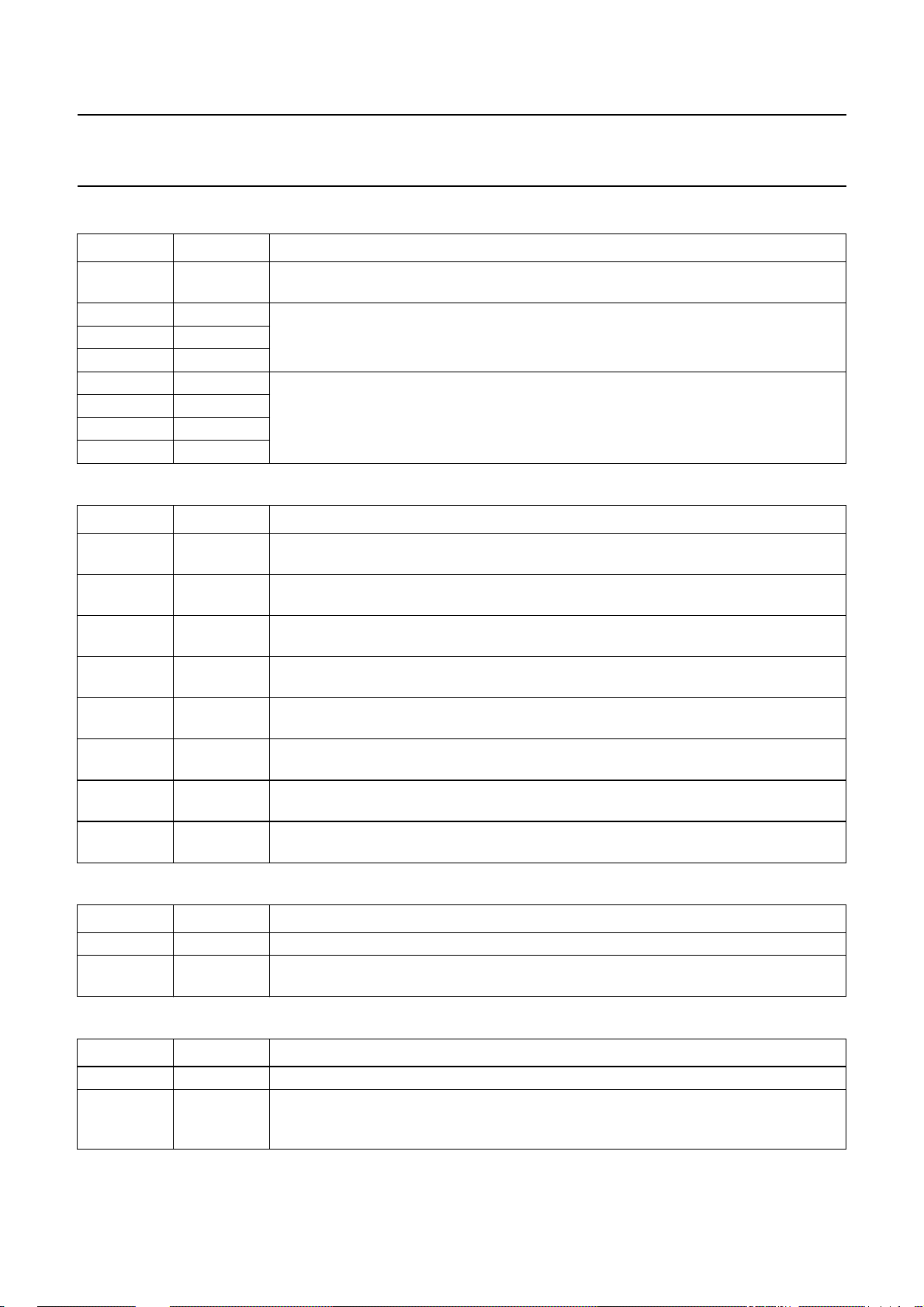
Table 12 Subaddress 2CH
BIT SYMBOL DESCRIPTION
7 CGEN 0 = copy generation data output is disabled; default state after reset
1 = copy generation data output is enabled
6 − These 3 bits are reserved; each must be set to logic 0.
5 −
4 −
3 CG19 Remaining bits of copy generation code.
2 CG18
1 CG17
0 CG16
Table 13 Subaddress 2DH
BIT SYMBOL DESCRIPTION
7 CVBSEN1 0 = luminance output signal is switched to Y DAC; default state after reset
1 = CVBS output signal is switched to Y DAC
6 CVBSEN0 0 = chrominance output signal is switched to C DAC; default state after reset
1 = CVBS output signal is switched to C DAC
5 CVBSTRI 0 = DAC for CVBS output in 3-state mode (high-impedance); default state after reset
1 = DAC for CVBS output in normal operation mode
4 YTRI 0 = DAC for Y output in 3-state mode (high-impedance); default state after reset
1 = DAC for Y output in normal operation mode
3 CTRI 0 = DAC for C output in 3-state mode (high-impedance); default state after reset
1 = DAC for C output in normal operation mode
2 RTRI 0 = DAC for RED output in 3-state mode (high-impedance); default state after reset
1 = DAC for RED output in normal operation mode
1 GTRI 0 = DAC for GREEN output in 3-state mode (high-impedance); default state after reset
1 = DAC for GREEN output in normal operation mode
0 BTRI 0 = DAC for BLUE output in 3-state mode (high-impedance); default state after reset
1 = DAC for BLUE output in normal operation mode
Table 14 Subaddress 38H
BIT SYMBOL DESCRIPTION
7to5 − These 3 bits are reserved; each must be set to logic 0.
4 to 0 GY[4:0] Gain luminance of RGB (C
Suggested nominal value = −6 (11010b), depending on external application.
Table 15 Subaddress 39H
BIT SYMBOL DESCRIPTION
7to5 − These 3 bits are reserved; each must be set to logic 0.
4 to 0 GCD[4:0] Gain colour difference of RGB (C
(1 −16⁄32)to(1+15⁄32). Suggested nominal value = −6 (11010b), depending on external
application.
2000 Mar 08 19
, Yand CB) output, ranging from (1 −16⁄32)to(1+15⁄32).
R
, Yand CB) output, ranging from
R
Page 20

Philips Semiconductors Product specification
Digital video encoder SAA7128H; SAA7129H
Table 16 Subaddress 3AH
BIT SYMBOL DESCRIPTION
7 CBENB 0 = data from input ports is encoded; default state after reset
1 = colour bar with fixed colours is encoded
6 − These 2 bits are reserved; each must be set to a logic 0.
5 −
4 SYMP 0 = horizontal and vertical trigger is taken from RCV2 and RCV1 respectively; default
state after reset
1 = horizontal and vertical trigger is decoded out of
MPEG port
3 DEMOFF 0 = YC
1=YCBCR-to-RGB dematrix is bypassed
2 CSYNC 0 = CVBS output signal is switched to CVBS DAC; default state after reset
1 = advanced composite sync is switched to CVBS DAC
1 MP2C 0 = input data is 2’s complement from MPEG port fader input
1 = input data is straight binary from MPEG port fader input; default state after reset
0 VP2C 0 = input data is 2’s complement from Video port fader input
1 = input data is straight binary from Video port fader input; default state after reset
-to-RGB dematrix is active; default state after reset
BCR
“ITU-R BT.656”
compatible data at
Table 17 Subaddresses 42H to 44H and 48H to 4AH
ADDRESS BYTE DESCRIPTION
42H
48H
43H
49H
44H
4AH
Table 18 Subaddresses 45H to 47H and 4BH to 4DH
ADDRESS BYTE DESCRIPTION
45H
4BH
46H
4CH
47H
4DH
KEY1LU
KEY1UU
KEY1LV
KEY1UV
KEY1LY
KEY1UY
KEY2LU
KEY2UU
KEY2LV
KEY2UV
KEY2LY
KEY2UY
Key colour 1 lower and upper limits for U, V and Y. If MPEG input signal is within the
limits of key colour 1 the incoming signals at the Video port and MPEG port are added
together according to the equation:
FADE1 × video signal + (1 − FADE1) × MPEG signal
Default value of all bytes after reset = 80H.
Key colour 2 lower and upper limits for U,V and Y. If MPEG input signal is within the
limits of key colour 2 the incoming signals at the Video port and MPEG port are added
together according to the equation:
FADE2 × video signal + (1 − FADE2) × LUT values
Default value of all bytes after reset = 80H.
2000 Mar 08 20
Page 21

Philips Semiconductors Product specification
Digital video encoder SAA7128H; SAA7129H
Table 19 Subaddress 4EH
BIT SYMBOL DESCRIPTION
7to6 − These 2 bits are reserved; each must be set to logic 0.
5 to 0 FADE1[5:0] These 6 bits form factor FADE1 which determines the ratio between the MPEG and
video input signal in the resulting video data stream if the key colour 1 is detected in the
MPEG input signal.
FADE1 = 00H: 100% MPEG, 0% video
FADE1 = 3FH: 100% video, 0% MPEG; this is the default value after reset
Table 20 Subaddress 4FH
BIT SYMBOL DESCRIPTION
7 CFADEM 0 = fader operates in normal mode; default state after reset
1 = the entire video input stream is faded with the colour stored in the LUT
(subaddresses 51H to 53H) regardless of the MPEG input signal. The colour keys are
disabled.
6 CFADEV 0 = fader operates in normal mode; default state after reset
1 = the entire MPEG input stream is faded with the colour stored in the LUT
(subaddresses 51H to 53H) regardless of the video input signal. The colour keys are
disabled.
5 to 0 FADE2[5:0] These 6 bits form factor FADE2 which determines the ratio between the LUT colour
values (subaddresses 51H to 53H) and the video input signal in the resulting video data
stream if the key colour 2 is detected in the MPEG input signal.
FADE2 = 00H: 100% LUT colour, 0% video
FADE2 = 3FH: 100% video, 0% LUT colour; this is the default value after reset
Table 21 Subaddress 50H
BIT SYMBOL DESCRIPTION
7to6 − These 2 bits are reserved; each must be a logic 0.
5 to 0 FADE3[5:0] These 6 bits form factor FADE3 which determines the ratio between the MPEG and
video input signal in the resulting video data stream if neither the key colour 1 nor the
key colour 2 is detected in the MPEG input signal.
FADE3 = 00H: 100% MPEG, 0% video
FADE3 = 3FH: 100% video, 0% MPEG; this is the default value after reset
2000 Mar 08 21
Page 22

Philips Semiconductors Product specification
Digital video encoder SAA7128H; SAA7129H
Table 22 Subaddress 51H
BIT SYMBOL DESCRIPTION
7 to 0 LUTU[7:0] LUTfor the colour valuesinserted incase of keycolour 2 U detection in the MPEG input
data stream.
LUTU[7:0] = 80H; default value after reset
Table 23 Subaddress 52H
BIT SYMBOL DESCRIPTION
7 to 0 LUTV[7:0] LUT for the colour values inserted in case of key colour 2 V detection in the MPEG input
data stream.
LUTV[7:0] = 80H; default value after reset
Table 24 Subaddress 53H
BIT SYMBOL DESCRIPTION
7 to 0 LUTY[7:0] LUT for the colour values inserted in case of key colour 2 Y detection in the MPEG input
data stream.
LUTY[7:0] = 80H; default value after reset
Table 25 Subaddress 54H
BIT SYMBOL DESCRIPTION
7 VPSEN 0 = video programming system data insertion is disabled; default state after reset
1 = video programming system data insertion in line 16 is enabled
6 − This bit is not used and should be set to logic 0.
5 ENCIN 0 = encoder path is fed with MP
input data; fader is bypassed; default state after reset
B
1 = encoder path is fed with output signal of fader; see Section 7.1
4 RGBIN 0 = RGB path is fed with MP
input data; fader is bypassed; default state after reset
B
1 = RGB path is fed with output signal of fader; see Section 7.1
3 DELIN 0 = not supported in current version; do not use
1 = recommended value; default state after reset
2 VPSEL 0 = not supported in current version; do not use
1 = recommended value; default state after reset
1 EDGE2 0 = MP
data is sampled on the rising clock edge; default state after reset
B
1=MPB data is sampled on the falling clock edge
0 EDGE1 0 = MP
data is sampled on the rising clock edge; default state after reset
A
1=MPA data is sampled on the falling clock edge
2000 Mar 08 22
Page 23

Philips Semiconductors Product specification
Digital video encoder SAA7128H; SAA7129H
Table 26 Subaddress 55H
BIT SYMBOL DESCRIPTION
7 to 0 VPS5[7:0] Fifth byte of video programming system data in line 16; LSB first.
Table 27 Subaddress 56H
BIT SYMBOL DESCRIPTION
7 to 0 VPS11[7:0] Eleventh byte of video programming system data in line 16; LSB first.
Table 28 Subaddress 57H
BIT SYMBOL DESCRIPTION
7 to 0 VPS12[7:0] Twelfth byte of video programming system data in line 16; LSB first.
Table 29 Subaddress 58H
BIT SYMBOL DESCRIPTION
7 to 0 VPS13[7:0] Thirteenth byte of video programming system data in line 16; LSB first.
Table 30 Subaddress 59H
BIT SYMBOL DESCRIPTION
7 to 0 VPS14[7:0] Fourteenth byte of video programming system data in line 16; LSB first.
Table 31 Subaddress 5AH
BIT SYMBOL DESCRIPTION
7 to 0 CHPS[7:0] Phase of encoded colour subcarrier (including burst) relative to horizontal sync; can be
adjusted in steps of 360/256 degrees.
0FH = PAL-B/G and data from input ports
3AH = PAL-B/G and data from look-up table
35H = NTSC-M and data from input ports
57H = NTSC-M and data from look-up table
2000 Mar 08 23
Page 24
Philips Semiconductors Product specification
Digital video encoder SAA7128H; SAA7129H
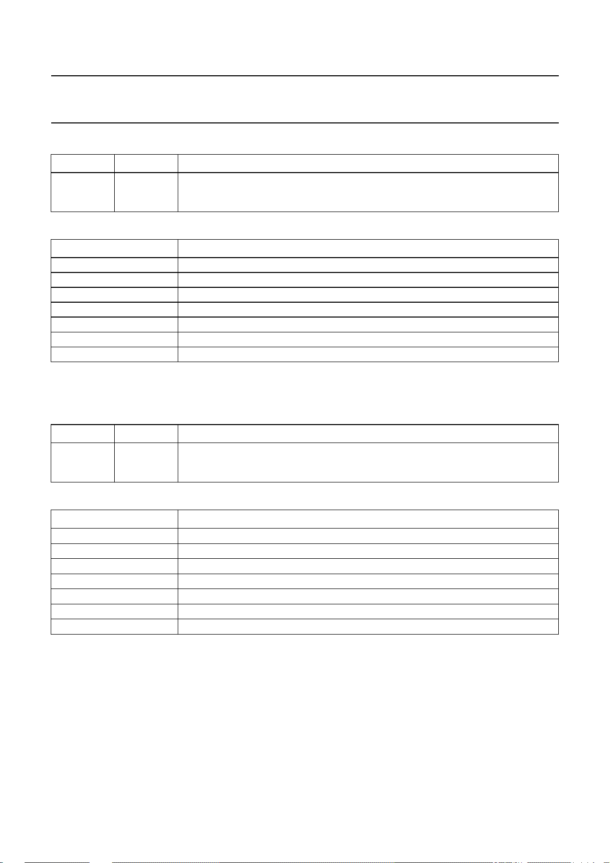
Table 32 Subaddress 5BH
BIT SYMBOL DESCRIPTION
7 to 0 GAINU[7:0] These are the 8 LSBs of the 9-bit code that selects the variable gain for the C
input representation in accordance with
“ITU-R BT.601”
; see Table 33. The MSB is held
in subaddress 5DH, see Table 36.
Table 33 GAINU values
CONDITIONS
(1)
ENCODING
white-to-black = 92.5 IRE GAINU = −2.17 × nominal to +2.16 × nominal
GAINU[8:0] = 0 output subcarrier of U contribution = 0
GAINU[8:0] = 118 (76H) output subcarrier of U contribution = nominal
white-to-black = 100 IRE GAINU = −2.05 × nominal to +2.04 × nominal
GAINU[8:0] = 0 output subcarrier of U contribution = 0
GAINU[8:0] = 125 (7DH) output subcarrier of U contribution = nominal
GAINU[8:0] = 106 (6AH) nominal GAINU for SECAM encoding
signal;
B
Note
1. All IRE values are rounded up
Table 34 Subaddress 5CH
BIT SYMBOL DESCRIPTION
7 to 0 GAINV[7:0] These are the 8 LSBs of the 9-bit code that selects the variable gain for the C
input representation in accordance with
“ITU-R BT.601”
; see Table 35. The MSB is held
in subaddress 5EH, see Table 38.
Table 35 GAINV values
CONDITIONS
(1)
ENCODING
white-to-black = 92.5 IRE GAINV = −1.55 × nominal to +1.55 × nominal
GAINV[8:0] = 0 output subcarrier of V contribution = 0
GAINV[8:0] = 165 (A5H) output subcarrier of V contribution = nominal
white-to-black = 100 IRE GAINV = −1.46 × nominal to +1.46 × nominal
GAINV[8:0] = 0 output subcarrier of V contribution = 0
GAINV[8:0] = 175 (AFH) output subcarrier of V contribution = nominal
GAINV[8:0] = 129 (81H) nominal GAINV for SECAM encoding
Note
1. All IRE values are rounded up.
signal;
R
2000 Mar 08 24
Page 25
Philips Semiconductors Product specification
Digital video encoder SAA7128H; SAA7129H
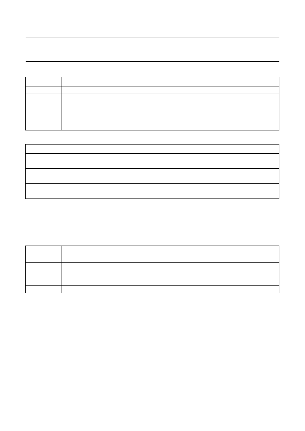
Table 36 Subaddress 5DH
BIT SYMBOL DESCRIPTION
7 GAINU8 MSB of the 9-bit code that sets the variable gain for the C
6 DECOE real-time control:
0 = disable odd/even field control bit from RTCI
1 = enable odd/even field control bit from RTCI (see Fig.22)
5 to 0 BLCKL[5:0] variable black level; input representation in accordance with
Table 37
Table 37 BLCKL values
CONDITIONS
(1)
ENCODING
white-to-sync = 140 IRE; note 2 recommended value: BLCKL = 58 (3AH)
BLCKL = 0; note 2 output black level = 29 IRE
BLCKL = 63 (3FH); note 2 output black level = 49 IRE
white-to-sync = 143 IRE; note 3 recommended value: BLCKL = 51 (33H)
BLCKL = 0; note 3 output black level = 27 IRE
BLCKL = 63 (3FH); note 3 output black level = 47 IRE
(1)
signal, see Table 32.
B
“ITU-R BT.601”
; see
Notes
1. All IRE values are rounded up.
2. Output black level/IRE = BLCKL × 2/6.29 + 28.9.
3. Output black level/IRE = BLCKL × 2/6.18 + 26.5.
Table 38 Subaddress 5EH
BIT SYMBOL DESCRIPTION
7 GAINV8 MSB of the 9-bit code that sets the variable gain for the C
6 DECPH real-time control:
0 = disable subcarrier phase reset bit from RTCI
1 = enable subcarrier phase reset bit from RTCI (see Fig.22)
5 to 0 BLNNL[5:0] variable blanking level, see Table 39
signal, see Table 34.
R
2000 Mar 08 25
Page 26

Philips Semiconductors Product specification
Digital video encoder SAA7128H; SAA7129H
Table 39 BLNNL values
CONDITIONS
white-to-sync = 140 IRE; note 2 recommended value: BLNNL = 46 (2EH)
BLNNL = 0; note 2 output blanking level = 25 IRE
BLNNL = 63 (3FH); note 2 output blanking level = 45 IRE
white-to-sync = 143 IRE; note 3 recommended value: BLNNL = 53 (35H)
BLNNL = 0; note 3 output blanking level = 26 IRE
BLNNL = 63 (3FH); note 3 output blanking level = 46 IRE
Notes
1. All IRE values are rounded up.
2. Output black level/IRE = BLNNL × 2/6.29 + 25.4.
3. Output black level/IRE = BLNNL × 2/6.18 + 25.9; default after reset: 35H.
Table 40 Subaddress 5FH
(1)
ENCODING
(1)
BIT SYMBOL DESCRIPTION
7 CCRS1 These 2 bits select the cross-colour reduction filter in luminance; see Table 41
6 CCRS0
5 BLNVB5 These 6 bits select the variable blanking level during vertical blanking interval is
4 BLNVB4
3 BLNVB3
2 BLNVB2
1 BLNVB1
0 BLNVB0
Table 41 Selection of cross-colour reduction filter
CCRS1 CCRS0 DESCRIPTION
0 0 no cross-colour reduction
0 1 cross-colour reduction #1 active
1 0 cross-colour reduction #2 active
1 1 cross-colour reduction #3 active
and Fig.10.
typically identical to value of BLNNL.
2000 Mar 08 26
Page 27

Philips Semiconductors Product specification
Digital video encoder SAA7128H; SAA7129H
Table 42 Subaddress 61H
BIT SYMBOL DESCRIPTION
7 DOWNB 0 = DACs for R, G and B in normal operational mode
1 = DACs for R, G and B forced to lowest output voltage; default state after reset
6 DOWNA 0 = DACs for CVBS, Y and C in normal operational mode; default state after reset
1 = DACs for CVBS, Y and C forced to lowest output voltage
5 INPI 0 = PAL switch phase is nominal; default state after reset
1 = PAL switch phase is inverted compared to nominal if RTC is enabled (see Table 43).
4 YGS 0 = luminance gain for white− black 100 IRE; default state after reset
1 = luminance gain for white − black 92.5 IRE including 7.5 IRE set-up of black
3 SECAM 0 = no SECAM encoding; default state after reset
1 = SECAM encoding activated; bit PAL has to be set to logic 0
2 SCBW 0 = enlarged bandwidth for chrominance encoding (for overall transfer characteristic of
chrominance in baseband representation see Figs 8 and 9)
1 = standard bandwidth for chrominance encoding (for overall transfer characteristic of
chrominance in baseband representation see Figs 8 and 9); default state after reset
1 PAL 0 = NTSC encoding (non-alternating V component)
1 = PAL encoding (alternating V component); default state after reset
0 FISE 0 = 864 total pixel clocks per line; default state after reset
1 = 858 total pixel clocks per line
Table 43 Subaddress 62H
BIT SYMBOL DESCRIPTION
7 RTCE 0 = no real-time control of generated subcarrier frequency; default state after reset
1 = real-time control of generated subcarrier frequency through SAA7151B or
SAA7111; for timing see Fig.22
6 to 0 BSTA[6:0] amplitude of colour burst; input representation in accordance with
Table 44
“ITU-R BT.601”
; see
2000 Mar 08 27
Page 28

Philips Semiconductors Product specification
Digital video encoder SAA7128H; SAA7129H
Table 44 BSTA values
CONDITIONS
white-to-black = 92.5 IRE;
burst = 40 IRE; NTSC encoding
BSTA = 0 to 2.02 × nominal
white-to-black = 92.5 IRE;
burst = 40 IRE; PAL encoding
BSTA = 0 to 2.82 × nominal
white-to-black = 100 IRE;
burst = 43 IRE; NTSC encoding
BSTA = 0 to 1.90 × nominal
white-to-black = 100 IRE;
burst = 43 IRE; PAL encoding
BSTA = 0 to 3.02 × nominal
fixed burst amplitude with SECAM encoding
(1)
ENCODING
recommended value: BSTA = 63 (3FH)
recommended value: BSTA = 45 (2DH)
recommended value: BSTA = 67 (43H)
recommended value: BSTA = 47 (2FH); default value after reset
Note
1. All IRE values are rounded up.
Table 45 Subaddresses 63H to 66H
ADDRESS BYTE DESCRIPTION
63H FSC[07:00] These 4 bytesare used to program the subcarrier frequency. FSC[31:24]is the most
significant byte, FSC[07:00] is the least significant byte.
64H FSC[15:08] f
65H FSC[23:16]
66H FSC[31:24]
= subcarrier frequency (in multiples of line frequency)
sc
f
= clock frequency (in multiples of line frequency)
llc
f
sc
FSC round
=
232×
------
f
llc
; note 1
Note
1. Examples:
a) NTSC-M: f
b) PAL-B/G: fsc= 283.7516, f
c) SECAM: fsc= 274.304, f
= 227.5, f
sc
= 1716 → FSC = 569408543 (21F07C1FH).
llc
= 1728 → FSC = 705268427 (2A098ACBH).
llc
= 1728 → FSC = 681786290 (28A33BB2H).
llc
2000 Mar 08 28
Page 29

Philips Semiconductors Product specification
Digital video encoder SAA7128H; SAA7129H
Table 46 Subaddress 67H
BIT SYMBOL DESCRIPTION
7 to 0 L21O[07:00] First byte of captioning data, odd field.
LSB of the byte is encoded immediately after run-in and framing code, the MSB of the
byte has to carry the parity bit, in accordance with the definition of line 21 encoding
format.
Table 47 Subaddress 68H
BIT SYMBOL DESCRIPTION
7 to 0 L21O[17:10] Second byte of captioning data, odd field.
The MSB of the byte has to carry the parity bit, in accordance with the definition of
line 21 encoding format.
Table 48 Subaddress 69H
BIT SYMBOL DESCRIPTION
7 to 0 L21E[07:00] First byte of extended data, even field.
LSB of the byte is encoded immediately after run-in and framing code, the MSB of the
byte has to carry the parity bit, in accordance with the definition of line 21 encoding
format.
Table 49 Subaddress 6AH
BIT SYMBOL DESCRIPTION
7 to 0 L21E[17:10] Second byte of extended data, even field.
The MSB of the byte has to carry the parity bit, in accordance with the definition of
line 21 encoding format.
2000 Mar 08 29
Page 30

Philips Semiconductors Product specification
Digital video encoder SAA7128H; SAA7129H
Table 50 Subaddress 6BH
BIT SYMBOL DESCRIPTION
7 SRCV11 These 2 bits define signal type on pin RCV1; see Table 51
6 SRCV10
5 TRCV2 0 = horizontal synchronization is taken from RCV1 port (at bit SYMP = LOW) or from
decoded frame sync of
reset
1 = horizontal synchronization is taken from RCV2 port (at bit SYMP = LOW)
4 ORCV1 0 = pin RCV1 is switched to input; default state after reset
1 = pin RCV1 is switched to output
3 PRCV1 0 = polarity of RCV1 as output is active HIGH, rising edge is taken when input; default
state after reset
1 = polarity of RCV1 as output is active LOW, falling edge is taken when input
2 CBLF When CBLF = 0.
If ORCV2 = 1, pin RCV2 provides an HREF signal (horizontal reference pulse that is
defined by RCV2S and RCV2E, also during vertical blanking interval); default state
after reset.
If ORCV2 = 0 and bit SYMP = 0, signal input to RCV2 is used for horizontal
synchronization only (if TRCV2 = 1); default state after reset.
When CBLF = 1.
If ORCV2 = 1, pin RCV2 provides a ‘composite-blanking-not’ signal, for example a
reference pulse that is defined by RCV2S and RCV2E, excluding vertical blanking
interval, which is defined by FAL and LAL.
If ORCV2 = 0 and bit SYMP = 0, signal input to RCV2 is used for horizontal
synchronization (if TRCV2 = 1) and as an internal blanking signal.
1 ORCV2 0 = pin RCV2 is switched to input; default state after reset
1 = pin RCV2 is switched to output
0 PRCV2 0 = polarity of RCV2 as output is active HIGH, rising edge is taken when input,
respectively; default state after reset
1 = polarity of RCV2 as output is active LOW, falling edge is taken when input,
respectively
“ITU-R BT.656”
input (at bit SYMP = HIGH); default state after
Table 51 Selection of the signal type on pin RCV1
SRCV11 SRCV10 RCV1 FUNCTION
0 0 VS Vertical Sync each field; default state after reset
0 1 FS Frame Sync (odd/even)
1 0 FSEQ Field Sequence, vertical sync every fourth field (PAL= 0), eighth field
(PAL = 1) or twelfth field (SECAM = 1)
11−not applicable
2000 Mar 08 30
Page 31

Philips Semiconductors Product specification
Digital video encoder SAA7128H; SAA7129H
Table 52 Subaddress 6CH
BIT SYMBOL DESCRIPTION
7 to 0 HTRIG[7:0] These are the 8 LSBs of the 11-bit code that sets the horizontal trigger phase related to
the signal on RCV1 or RCV2 input. The 3 MSBs are held in subaddress 6DH, see
Table 53. Values above 1715 (FISE = 1) or 1727 (FISE = 0) are not allowed. Increasing
HTRIG[10:0] decreases delays of all internally generated timing signals. Reference
mark: analog output horizontal sync (leading slope) coincides with active edge of RCV
used for triggering at HTRIG[10:0] = 4FH (79).
Table 53 Subaddress 6DH
BIT SYMBOL DESCRIPTION
7 HTRIG10 These are the 3 MSBs of the horizontal trigger phase code; see Table52.
6 HTRIG9
5 HTRIG8
4 VTRIG4 Sets the vertical trigger phase related to signal on RCV1 input. Increasing VTRIG
3 VTRIG3
2 VTRIG2
1 VTRIG1
0 VTRIG0
decreases delays of all internally generated timing signals, measured in half lines;
variation range of VTRIG[4:0] = 0 to 31 (1FH).
Table 54 Subaddress 6EH
BIT SYMBOL DESCRIPTION
7 SBLBN 0 = vertical blanking is defined by programming of FAL and LAL; default state after reset
1 = vertical blanking is forced in accordance with
(60 Hz)
6 BLCKON 0 = encoder in normal operation mode
1 = output signal is forced to blanking level; default state after reset
5 PHRES1 These 2 bits select the phase reset mode of the colour subcarrier generator;
4 PHRES0
3 LDEL1 These 2 bits select the delay on luminance path with reference to chrominance path;
2 LDEL0
1 FLC1 These 2 bits select field length control; see Table 57.
0 FLC0
Table 55 Selection of phase reset mode
PHRES1 PHRES0 DESCRIPTION
0 0 no reset or reset via RTCI from SAA7111 if bit RTCE = 1; default value after reset
0 1 reset every two lines or SECAM specific if bit SECAM = 1
1 0 reset every eight fields
1 1 reset every four fields
see Table 55.
see Table 56.
“ITU-R BT.624”
(50 Hz) or RS170A
2000 Mar 08 31
Page 32
Philips Semiconductors Product specification
Digital video encoder SAA7128H; SAA7129H
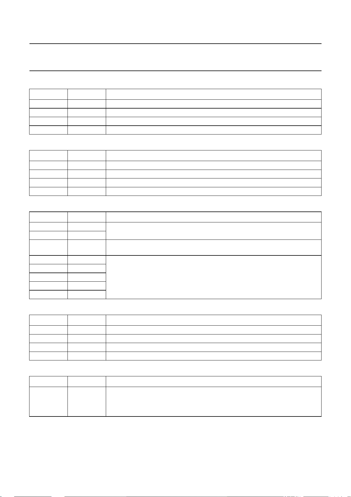
Table 56 Selection of luminance path delay
LDEL1 LDEL0 LUMINANCE PATH DELAY
0 0 no luminance delay; default value after reset
0 1 1 LLC luminance delay
1 0 2 LLC luminance delay
1 1 3 LLC luminance delay
Table 57 Selection of field length control
FLC1 FLC0 DESCRIPTION
0 0 interlaced 312.5 lines/field at 50 Hz, 262.5 lines/field at 60 Hz; default value after reset
0 1 non-interlaced 312 lines/field at 50 Hz, 262 lines/field at 60 Hz
1 0 non-interlaced 313 lines/field at 50 Hz, 263 lines/field at 60 Hz
1 1 non-interlaced 313 lines/field at 50 Hz, 263 lines/field at 60 Hz
Table 58 Subaddress 6FH
BIT SYMBOL DESCRIPTION
7 CCEN1 These 2 bits enable individual line 21 encoding; see Table 59.
6 CCEN0
5 TTXEN 0 = disables teletext insertion; default state after reset
1 = enables teletext insertion
4 SCCLN4 These 5 bits select the actual line where closed caption or extended data are encoded.
3 SCCLN3 line = (SCCLN[4:0] + 4) for M-systems
2 SCCLN2
1 SCCLN1
0 SCCLN0
Table 59 Selection of line 21 encoding
CCEN1 CCEN0 LINE 21 ENCODING
0 0 line 21 encoding off; default value after reset
0 1 enables encoding in field 1 (odd)
1 0 enables encoding in field 2 (even)
1 1 enables encoding in both fields
Table 60 Subaddress 70H
BIT SYMBOL DESCRIPTION
7 to 0 RCV2S[7:0] These are the 8 LSBs of the 11-bit code that determines the start of the output signal
line = (SCCLN[4:0] + 1) for other systems
on the RCV2 pin; the 3 MSBs of the 11-bit code are held at subaddress 72H (see
Table 62). Values above 1715 (FISE = 1) or 1727 (FISE = 0) are not allowed. Leading
sync slope at CVBS output coincides with leading slope of RCV2 out at RCV2S = 49H.
2000 Mar 08 32
Page 33
Philips Semiconductors Product specification
Digital video encoder SAA7128H; SAA7129H
Table 61 Subaddress 71H
BIT SYMBOL DESCRIPTION
7 to 0 RCV2E[7:0] These are the 8 LSBs of the 11-bit code that determines the end of the output signal
on the RCV2 pin; the 3 MSBs of the 11-bit code are held at subaddress 72H (see
Table 62). Values above 1715 (FISE = 1) or 1727 (FISE = 0) are not allowed. Leading
sync slope at CVBS output coincides with trailing slope of RCV2 out at RCV2E = 49H.
Table 62 Subaddress 72H
BIT SYMBOL DESCRIPTION
7 − This bit is reserved and must be set to a logic 0.
6 RCV2E10 These are the 3 MSBs of end of output signal code; see Table 61.
5 RCV2E9
4 RCV2E8
3 − This bit is reserved and must be set to a logic 0.
2 RCV2S10 These are the 3 MSBs of start of output signal code; see Table 60.
1 RCV2S9
0 RCV2S8
Table 63 Subaddress 73H
BIT SYMBOL DESCRIPTION
7 to 0 TTXHS[7:0] Start of signal on pin TTXRQ; see Fig.23.
PAL: TTXHS[7:0] = 42H
NTSC: TTXHS[7:0] = 54H
Table 64 Subaddress 74H
BIT SYMBOL DESCRIPTION
7 to 0 TTXHD[7:0] Indicates the delay in clock cycles between rising edge of TTXRQ output and valid
data at pin TTX.
minimum value: TTXHD[7:0] = 2
Table 65 Subaddress 75H
BIT SYMBOL DESCRIPTION
7 CSYNCA4 Advanced composite sync against RGB output from 0 to 31 LLC clock periods.
6 CSYNCA3
5 CSYNCA2
4 CSYNCA1
3 CSYNCA0
2 VS_S2 Vertical sync shift between RCV1 and RCV2 (switched to output); in master mode it is
1 VS_S1
0 VS_S0
possible to shift Hsync (RCV2; CBLF = 0) against Vsync (RCV1; SRCV1 = 00)
standard value: VS_S[2:0] = 3.
2000 Mar 08 33
Page 34

Philips Semiconductors Product specification
Digital video encoder SAA7128H; SAA7129H
Table 66 Subaddress 76H
BIT SYMBOL DESCRIPTION REMARKS
7 to 0 TTXOVS[7:0] These are the 8 LSBs of the 9-bit code that determines the
first line of occurrence of signal on pin TTXRQ in odd field;
the MSB is held in subaddress 7CH (see Table 72).
line = (TTXOVS[8:0] + 4) for M-systems
line = (TTXOVS[8:0] + 1) for other systems
Table 67 Subaddress 77H
BIT SYMBOL DESCRIPTION REMARKS
7 to 0 TTXOVE[7:0] These are the 8 LSBs of the 9-bit code that determines the
last line of occurrence of signal on pin TTXRQ in odd field.
The MSB is held in subaddress 7CH, see Table 72.
last line = (TTXOVE[8:0] + 3) for M-systems
last line = TTXOVE[8:0] for other systems
PAL: TTXOVS = 05H;
NTSC: TTXOVS = 06H
PAL: TTXOVE = 16H;
NTSC: TTXOVE = 10H
Table 68 Subaddress 78H
BIT SYMBOL DESCRIPTION REMARKS
7 to 0 TTXEVS[7:0] These are the 8 LSBs of the 9-bit code that determines the
first line of occurrence of signal on pin TTXRQ in even field.
The MSB is held in subaddress 7CH, see Table 72.
first line = (TTXEVS[8:0] + 4) for M-systems
first line = (TTXEVS[8:0] + 1) for other systems
Table 69 Subaddress 79H
BIT SYMBOL DESCRIPTION REMARKS
7 to 0 TTXEVE[7:0] These are the 8 LSBs of the 9-bit code that determines the
last line of occurrence of signal on pin TTXRQ in even field.
The MSB is held in subaddress 7CH, see Table 72.
last line = (TTXEVE[8:0] + 3) for M-systems
last line = TTXEVE [8:0]for other systems
Table 70 Subaddress 7AH
BIT SYMBOL DESCRIPTION
7 to 0 FAL[7:0] These are the 8 LSBs of the 9-bit code that determines the first active line. The MSB
is held in subaddress 7CH, see Table 72. FAL[8:0] = 0 coincides with the first field
synchronization pulse.
first active line = FAL[8:0] + 4 for M-systems
first active line = FAL[8:0] + 1 for other systems
PAL: TTXEVS = 04H;
NTSC: TTXEVS = 05H
PAL: TTXEVE = 16H;
NTSC: TTXEVE = 10H
2000 Mar 08 34
Page 35

Philips Semiconductors Product specification
Digital video encoder SAA7128H; SAA7129H
Table 71 Subaddress 7BH
BIT SYMBOL DESCRIPTION
7 to 0 LAL[7:0] These are the 8 LSBs of the 9-bit code that determines the last active line.The MSB is
held in subaddress 7CH, see Table 72. LAL[8:0] = 0 coincides with the first field
synchronization pulse.
last active line = LAL[8:0] + 3 for M-systems
last active line = LAL[8:0] for other systems
Table 72 Subaddress 7CH
BIT SYMBOL DESCRIPTION
7 TTX60 0 = enables NABTS (FISE = 1) or European teletext (FISE = 0); default state after
reset
1 = enables World Standard Teletext 60 Hz (FISE = 1)
6 LAL8 MSB of the last active line code; see Table 71.
5 TTXO 0 = new teletext protocol selected: at each rising edge of TTXRQ a single teletext bit is
requested (see Fig.23); default state after reset
1 = old teletext protocol selected: the encoder provides a window of TTXRQ going
HIGH; the length of the window depends on the chosen teletext standard (see Fig.23)
4 FAL8 MSB of the first active line code; see Table 70.
3 TTXEVE8 MSB of the 9-bit code that selects the last line of occurrence ofsignal on pin TTXRQ in
even field; see Table 69.
2 TTXOVE8 MSB of the 9-bit code that selects the last line of occurrenceof signal on pin TTXRQ in
odd field; see Table 67.
1 TTXEVS8 MSB of the9-bit code thatselects the firstline of occurrenceof signal onpin TTXRQ in
even field; see Table 68.
0 TTXOVS8 MSB ofthe 9-bit codethat selects thefirst line ofoccurrence of signalon pin TTXRQin
odd field; see Table 66.
Table 73 Subaddress 7EH
BIT SYMBOL DESCRIPTION
7 to 0 LINE[12:5] Individual lines in both fields (PAL counting) can be disabled for insertion of teletext by
the respective LINE bits. Disabled line = LINEnn (50 Hz field rate). This bit mask is
effective only, if the lines are enabled by TTXOVS/TTXOVE and TTXEVS/TTXEVE.
Table 74 Subaddress 7FH
SYMBOL SYMBOL DESCRIPTION
7 to 0 LINE[20:13] Individual lines in both fields (PAL counting) can be disabled for insertion of teletext by
the respective LINE bits. Disabled line = LINEnn (50 Hz field rate). This bit mask is
effective only, if the lines are enabled by TTXOVS/TTXOVE and TTXEVS/TTXEVE.
2000 Mar 08 35
Page 36

Philips Semiconductors Product specification
Digital video encoder SAA7128H; SAA7129H
7.14 Slave transmitter
The slave transmitter slave address is 89H.
Table 75 Subaddress 00H
BIT SYMBOL DESCRIPTION
7 VER2 These 3 bits form the version identification number of the device: it will be changed with
6 VER1
5 VER0
4 CCRDO 1 = closed caption bytes of the odd field have been encoded
3 CCRDE 1 = closed caption bytes of the even field have been encoded
2 − not used; set to logic 0
1 FSEQ 1 = during first field of a sequence (repetition rate: NTSC = 4 fields, PAL = 8 fields,
0 O_E 1 = during even field
all versions of the IC that have different programming models; current version is
000 binary.
0 = the bitis reset after information has been written to the subaddresses 67H and 68H;
it is set immediately after the data has been encoded
0 = the bit is reset after information has been written to the subaddresses 69H and 6AH;
it is set immediately after the data has been encoded
SECAM = 12 fields)
0 = not first field of a sequence
0 = during odd field
2000 Mar 08 36
Page 37
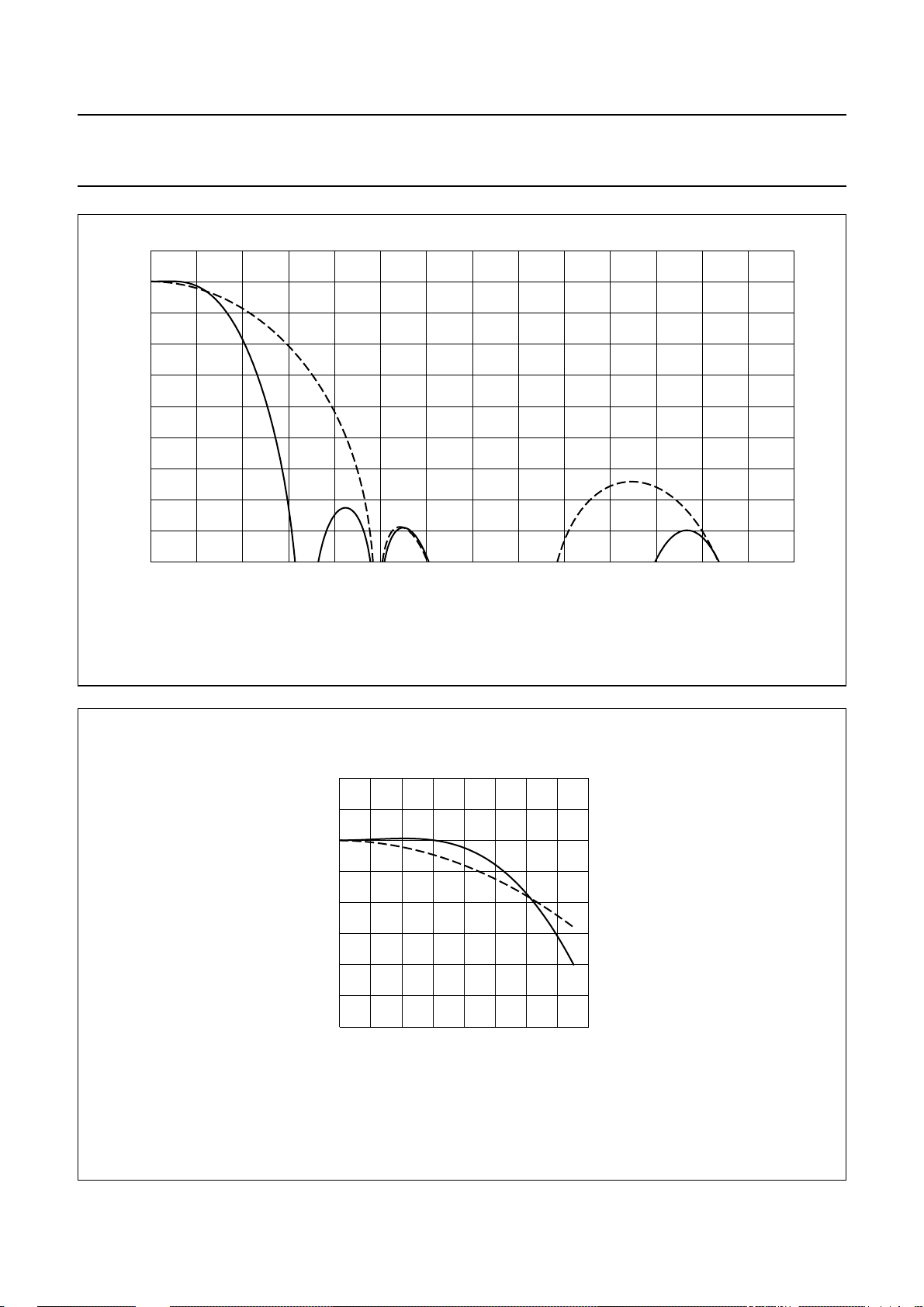
Philips Semiconductors Product specification
Digital video encoder SAA7128H; SAA7129H
handbook, full pagewidth
6
G
v
(dB)
0
−6
−12
−18
−24
−30
−36
−42
−48
−54
024
(1) SCBW = 1.
(2) SCBW = 0.
(1) (2)
Fig.8 Chrominance transfer characteristic 1.
MBE737
6 8 10 12 14
f (MHz)
handbook, halfpage
(1) SCBW = 1.
(2) SCBW = 0.
2
G
v
(dB)
0
−2
−4
−6
0 0.4 0.8 1.6
Fig.9 Chrominance transfer characteristic 2.
2000 Mar 08 37
MBE735
(1)
(2)
1.2
f (MHz)
Page 38
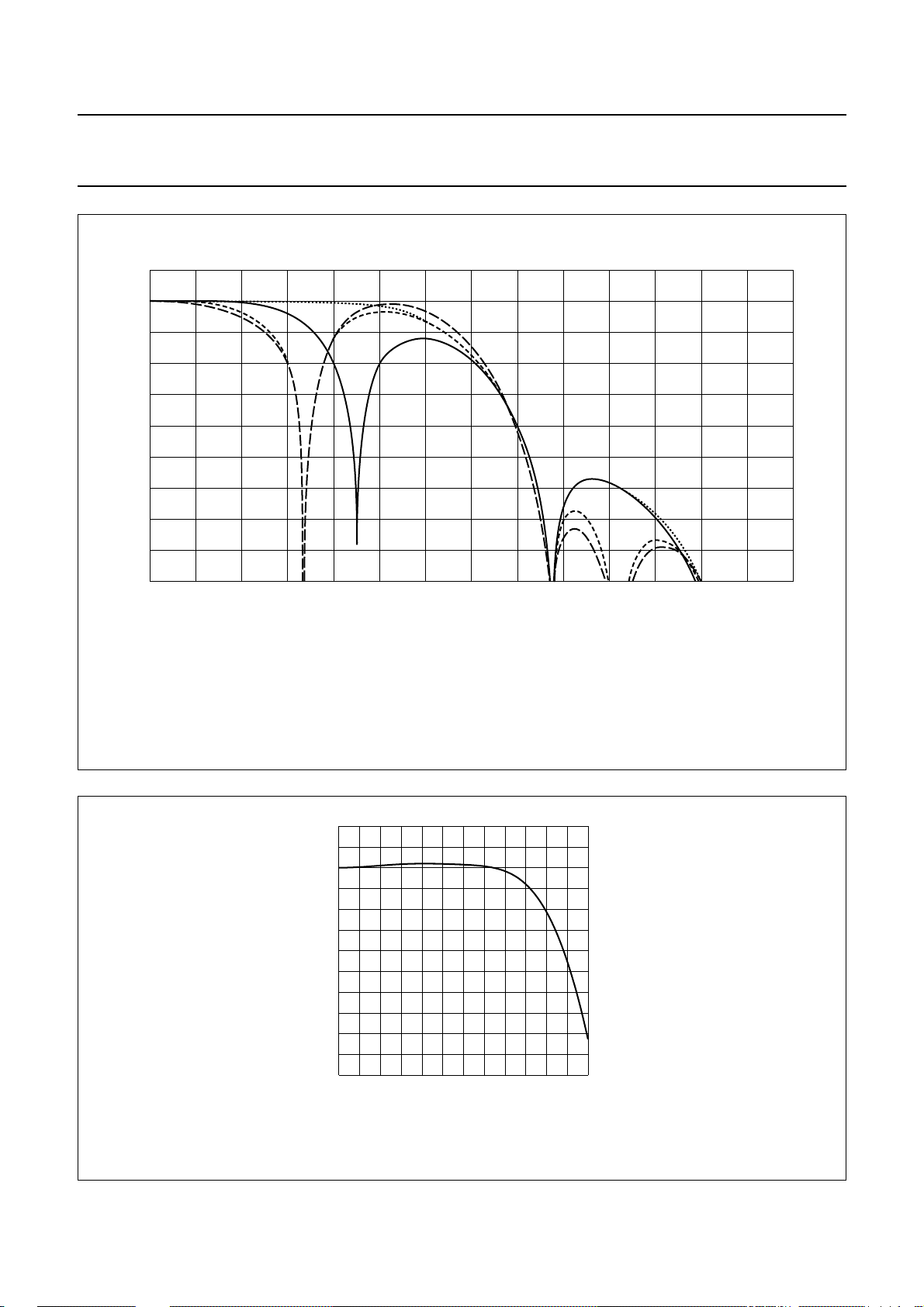
Philips Semiconductors Product specification
Digital video encoder SAA7128H; SAA7129H
6
G
handbook, full pagewidth
v
(dB)
0
−6
−12
−18
−24
−30
−36
−42
−48
−54
024
(1) CCRS1 = 0; CCRS0 = 1.
(2) CCRS1 = 1; CCRS0 = 0.
(3) CCRS1 = 1; CCRS0 = 1.
(4) CCRS1 = 0; CCRS0 = 0.
MGD672
(4)
(3)
(2)
(1)
6
8101214
f (MHz)
(1) CCRS1 = 0; CCRS0 = 0.
Fig.10 Luminance transfer characteristic 1.
handbook, halfpage
1
G
v
(dB)
0
−1
−2
−3
−4
−5
02
(1)
4
Fig.11 Luminance transfer characteristic 2.
f (MHz)
MBE736
6
2000 Mar 08 38
Page 39

Philips Semiconductors Product specification
Digital video encoder SAA7128H; SAA7129H
handbook, full pagewidth
6
G
v
(dB)
0
−6
−12
−18
−24
−30
−36
−42
−48
−54
024
6 8 10 12 14
Fig.12 Luminance transfer characteristic in RGB.
MGB708
f (MHz)
handbook, full pagewidth
6
G
v
(dB)
0
−6
−12
−18
−24
−30
−36
−42
−48
−54
024
6 8 10 12 14
Fig.13 Colour difference transfer characteristic in RGB.
2000 Mar 08 39
MGB706
f (MHz)
Page 40
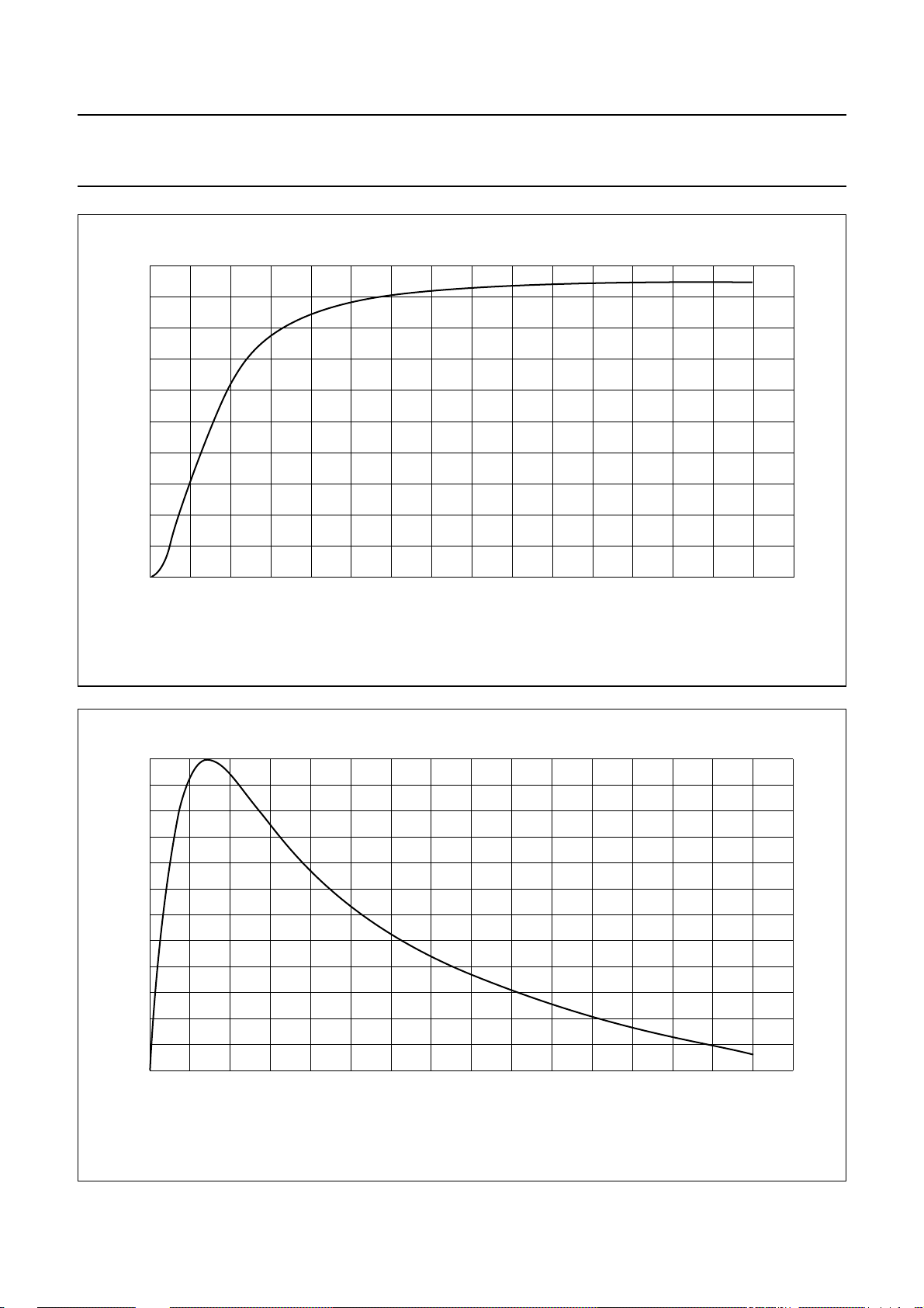
Philips Semiconductors Product specification
Digital video encoder SAA7128H; SAA7129H
handbook, full pagewidth
10
G
v
(dB)
8
6
4
2
0
0 0.2 0.4 1.4 1.60.8 1 1.2
MGB705
0.6
f (MHz)
Fig.14 Gain of SECAM pre-emphasis.
handbook, full pagewidth
30
ϕ
(deg)
20
10
0
0 0.2 0.4 1.4 1.60.8 1 1.2
MGB704
0.6
f (MHz)
Fig.15 Phase of SECAM pre-emphasis.
2000 Mar 08 40
Page 41
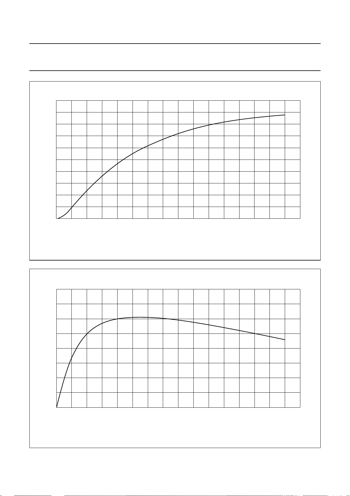
Philips Semiconductors Product specification
Digital video encoder SAA7128H; SAA7129H
handbook, full pagewidth
20
G
v
(dB)
16
12
8
4
0
0 0.2 0.4 1.4 1.60.8 1 1.2
MGB703
0.6
f (MHz)
Fig.16 Gain of SECAM anti-Cloche.
handbook, full pagewidth
80
ϕ
(deg)
60
40
20
0
0 0.2 0.4 1.4 1.60.8 1 1.2
MGB702
0.6
f (MHz)
Fig.17 Phase of SECAM anti-Cloche.
2000 Mar 08 41
Page 42
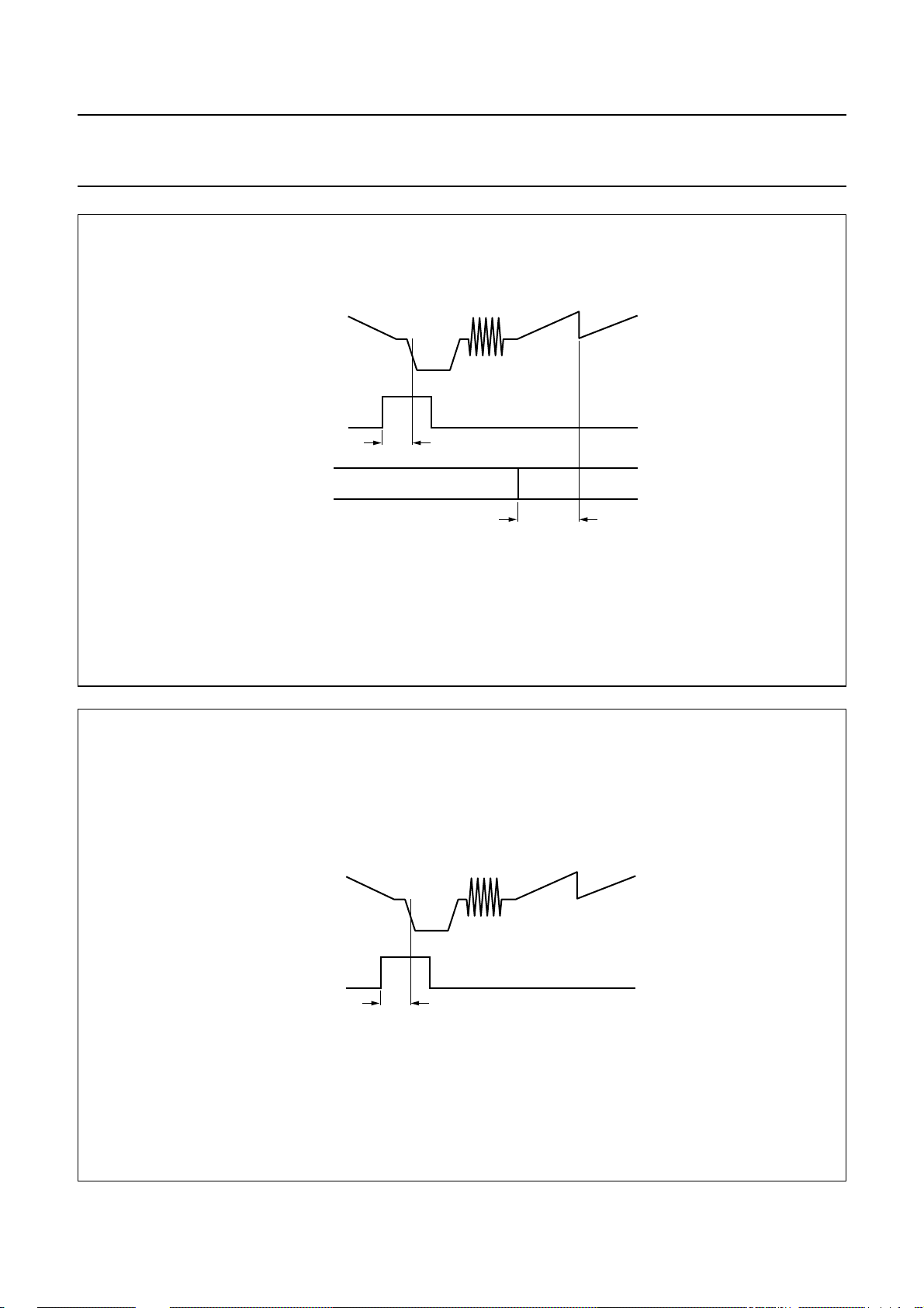
Philips Semiconductors Product specification
Digital video encoder SAA7128H; SAA7129H
handbook, full pagewidth
CVBS output
RCV2 input
79LCC
MP input
HTRIG = 0
PRCV2 = 0.
TRCV2 = 1.
ORCV2 = 0.
handbook, full pagewidth
82LCC
MHB579
Fig.18 Sync and video input timing.
CVBS output
RCV2 output
73LCC
RCV2S = 0.
PRCV2 = 0.
ORCV2 = 1.
Fig.19 Sync and video output timing.
2000 Mar 08 42
MHB580
Page 43

Philips Semiconductors Product specification
Digital video encoder SAA7128H; SAA7129H
8 CHARACTERISTICS
V
= 3.0 to 3.6 V; T
DDD
SYMBOL PARAMETER CONDITIONS MIN. MAX. UNIT
Supply
V
V
I
DDA
I
DDD
DDA
DDD
analog supply voltage 3.15 3.45 V
digital supply voltage 3.0 3.6 V
analog supply current note 1 − 150 mA
digital supply current V
Inputs: LLC1, RCV1, RCV2, MP7 to MP0, RTCI, SA, RESET and TTX
V
IL
V
IH
I
LI
C
i
LOW-level input voltage −0.5 +0.8 V
HIGH-level input voltage 2.0 V
input leakage current − 1 µA
input capacitance clocks − 10 pF
Outputs: RCV1, RCV2 and TTXRQ
V
OL
V
OH
2
C-bus: SDA and SCL
I
V
IL
V
IH
I
i
V
OL
I
o
LOW-level output voltage IOL=2mA − 0.4 V
HIGH-level output voltage IOH= −2 mA 2.4 − V
LOW-level input voltage −0.5 +0.3V
HIGH-level input voltage 0.7V
input current Vi= LOW or HIGH −10 +10 µA
LOW-level output voltage (pin SDA) IOL=3mA − 0.4 V
output current during acknowledge 3 − mA
Clock timing: LLC1 and XCLK
T
LLC1
cycle time note 2 34 41 ns
δ duty factor t
δ duty factor t
t
r
t
f
rise time note 2 − 5ns
fall time note 2 − 6ns
Input timing: RCV1, RCV2, MP7 to MP0, RTCI, SA and TTX
t
SU;DAT
t
HD;DAT
input data set-up time 6 − ns
input data hold time 3 − ns
= 0 to 70 °C; unless otherwise specified.
amb
HIGH/TLLC1
HIGH/TXCLK
= 3.3 V; note 1 − 100 mA
DDD
+ 0.3 V
DDD
data − 8pF
I/Os at
− 8pF
high-impedance
V
+ 0.3 V
DD(I2C)
V
DD(I2C)
DD(I2C)
LLC1 input 40 60 %
XCLK output typical
40 60 %
50%
2000 Mar 08 43
Page 44

Philips Semiconductors Product specification
Digital video encoder SAA7128H; SAA7129H
SYMBOL PARAMETER CONDITIONS MIN. MAX. UNIT
Crystal oscillator
f
n
∆f/f
n
CRYSTAL SPECIFICATION
T
amb
C
L
R
S
C
mot
C
par
Data and reference signal output timing
C
L
t
h
t
d
Outputs: C, VBS, CVBS and RGB
V
o(p-p)
∆V inequality of output signal voltages note 5 − 2%
R
int
R
L
B output signal bandwidth of DACs −3dB 10 − MHz
LE
lf(i)
LE
lf(d)
t
d(pipe)(MP)
Notes
1. At maximum supply voltage with highly active input signals.
2. The data is for both input and output direction.
3. If an internal oscillator is used, crystal deviation of nominal frequency is directly proportional to the deviation of
subcarrier frequency and line/field frequency.
4. For full digital range, without load, V
voltage (digital zero at DAC) is 0.2 V.
5. Referring to peak-to-peak analog voltages resulting from identical peak-to-peak digital codes.
nominal frequency (usually 27 MHz) 3rd harmonic − 30 MHz
permissible deviation of nominal
note 3 −50 +50 10
−6
frequency
ambient temperature 0 70 °C
load capacitance 8 − pF
series resistance − 80 Ω
motional capacitance (typical) 1.5 − 20% 1.5 + 20% fF
parallel capacitance (typical) 3.5 − 20% 3.5 + 20% pF
output load capacitance 7.5 40 pF
output hold time 4 − ns
output delay time − 18 ns
output signal voltage (peak-to-peak value) note 4 1.25 1.50 V
internal serial resistance 1 3 Ω
output load resistance 75 300 Ω
low frequency integral linearity error of
−±3 LSB
DACs
low frequency differential linearity error of
−±1 LSB
DACs
total pipeline delay from MP port 27 MHz − 82 LLC
= 3.3 V. The typical voltage swing is 1.35 V, the typical minimum output
DDA
2000 Mar 08 44
Page 45
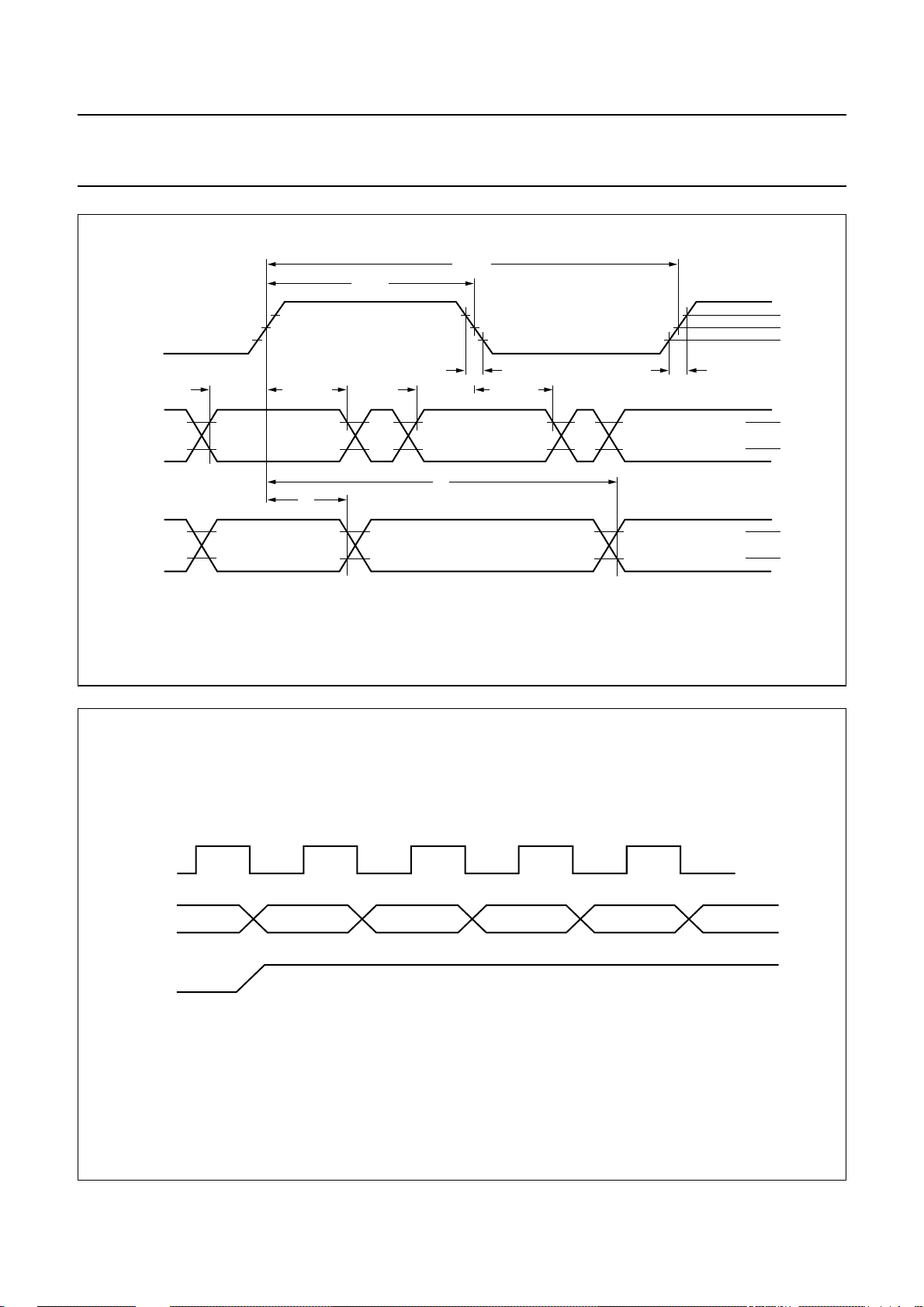
Philips Semiconductors Product specification
Digital video encoder SAA7128H; SAA7129H
handbook, full pagewidth
LLC1
MP input data
output data
t
SU; DATtHD; DAT
MP
pos
t
h
valid not valid
T
LLC1
t
HIGH
t
f
t
SU; DATtHD; DAT
not
valid
MP
t
d
Fig.20 Clock data timing.
neg
not
valid
2.6 V
1.5 V
0.6 V
t
r
MP
pos
valid
2.0 V
0.8 V
2.4 V
0.6 V
MHB581
handbook, full pagewidth
LLC
MP(n)
RCV2
The data demultiplexing phase is coupled to the internal horizontal phase.
The phase of the RCV2 signal is programmed to tbf (tbf for 50 Hz) in this example in output mode (RCV2S).
CB(0)
Y(0)
CR(0)
Fig.21 Functional timing.
2000 Mar 08 45
Y(1)
CB(2)
MGB699
Page 46

Philips Semiconductors Product specification
Digital video encoder SAA7128H; SAA7129H
8.1 Explanation of RTCI data bits
1. The HPLL increment is not evaluated by the
SAA7128H; SAA7129H.
2. The SAA7128H; SAA7129H generates the subcarrier
frequency from the FSCPLL increment ifenabled (see
item 7).
3. The PAL bit indicates the line with inverted (R − Y)
component of colour difference signal.
4. If the reset bit is enabled (RTCE = 1; DECPH = 1;
PHRES = 00), the phase of the subcarrier is reset in
each line whenever the reset bit of RTCI input is set to
logic 1.
5. If theFISE bit isenabled (RTCE = 1;DECFIS = 1), the
SAA7128H; SAA7129H takes this bit instead of the
FISE bit in subaddress 61H.
handbook, full pagewidth
RTCI
HIGH-to-LOW transition
count start
128
LOW
13
HPLL
increment
(1)
4 bits
reserved
0 022
6. If theodd/even bitis enabled(RTCE = 1;DECOE = 1),
the SAA7128H; SAA7129H ignores it’s internally
generated odd/even flag and takes the odd/even bit
from RTCI input.
7. If the colour detection bit is enabled (RTCE = 1;
DECCOL = 1) and no colour was detected (colour
detection bit = 0), the subcarrier frequency is
generated by the SAA7128H;SAA7129H. In the other
case (colour detection bit = 1) the subcarrier
frequency is evaluated out of FSCPLL increment.
If the colour detection bit is disabled (RTCE = 1;
DECCOL = 0), the subcarrier frequency is evaluated
out of FSCPLL increment, independent of the colour
detection bit of RTCI input.
3 bits
FSCPLL increment
reserved
(2)
(5)
(7)
(4)
(6)
(3)
time slot:
(1) SAA7111/12 provides 14 to 0 bits, resulting in 2 reserved bits before FSCPLL increment.
(2) SAA7151 provides 21 to 0 bits only, resulting in 5 reserved bits before sequence bit.
(3) Sequence bit: PAL: 0 = (R − Y) line normal, 1 = (R − Y) line inverted; NTSC: 0 = no change.
(4) Reset bit: only from SAA7111 and SAA7112 decoder.
(5) FISE bit: 0 = 50 Hz, 1 = 60 Hz.
(6) Odd/even bit: odd_even from external.
(7) Colour detection: 0 = no colour detected, 1 = colour detected.
(8) Reserved bits: 229 with 50 Hz systems, 226 with 60 Hz systems.
01
not used in SAA7128H/29H
14 19
valid
sample
Fig.22 RTCI timing.
invalid
sample
8/LLC
6764 69 72 74
68
MGL934
(8)
2000 Mar 08 46
Page 47
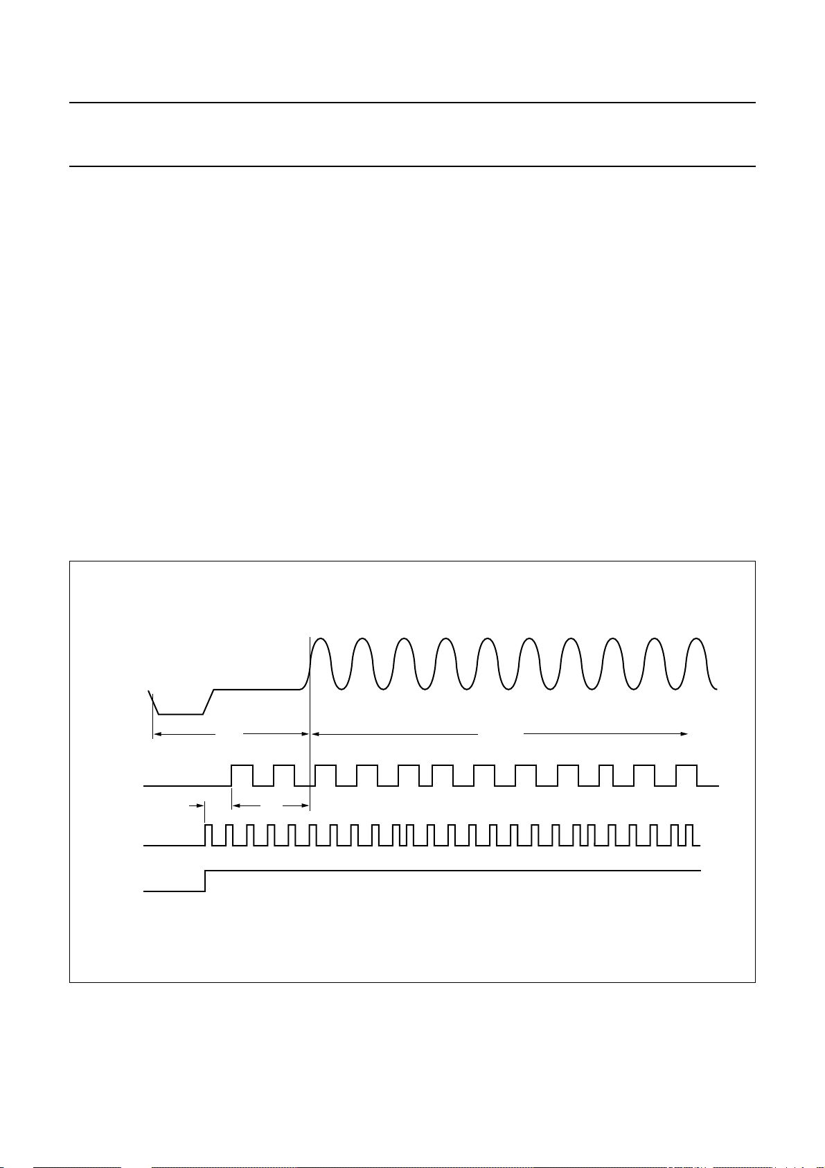
Philips Semiconductors Product specification
Digital video encoder SAA7128H; SAA7129H
8.2 Teletext timing
Time tFD is the time needed to interpolate input data TTX
and insert it into the CVBS and VBS output signal, such
that it appears at t
= 9.78 µs (PAL) or t
TTX
TTX
= 10.5 µs
(NTSC) after the leading edge of the horizontal
synchronization pulse.
Time tPD is the pipeline delay time introduced by the
source that is gated by TTXRQ in order to deliver TTX
data. This delay is programmable by register TTXHD.
For every active HIGH state at output pin TTXRQ, a new
teletext bit must be provided by the source (new protocol)
or a window of TTXRQ going HIGH is provided and the
number of teletext bits, depending on the chosen teletext
standard, is requested at input pin TTX (old protocol).
Sincethe beginningofthe pulsesrepresentingthe TTXRQ
signal and the delay between the rising edge of TTXRQ
and valid teletext input data are fully programmable
(TTXHS and TTXHD), the TTX data is always inserted at
the correct position after the leading edge of outgoing
horizontal synchronization pulse.
Time t
is the internally used insertion window for
i(TTXW)
TTX data; it has a constant length that allows insertion of
360 teletext bits at a text data rate of 6.9375 Mbits/s
(PAL),296 teletext bits atatext data rateof5.7272 Mbits/s
(WST) or 288 teletext bits at a text data rate of
5.7272 Mbits/s (NABTS). The insertion window is not
opened if the control bit TTXEN is zero.
Using appropriate programming, all suitable lines of the
odd field(TTXOVS and TTXOVE) plus all suitable lines of
the even field (TTXEVS and TTXEVE) can be used for
teletext insertion.
handbook, full pagewidth
CVBS/Y
TTX
TTXRQ (new)
TTXRQ (old)
t
TTX
text bit #: 1 2 3 4 5 6 7 8 9 10 11 12 13 14 15 16 17 18 19 20 21 22 23 24
t
PD
t
FD
t
i(TTXW)
MHB504
Fig.23 Teletext timing.
2000 Mar 08 47
Page 48
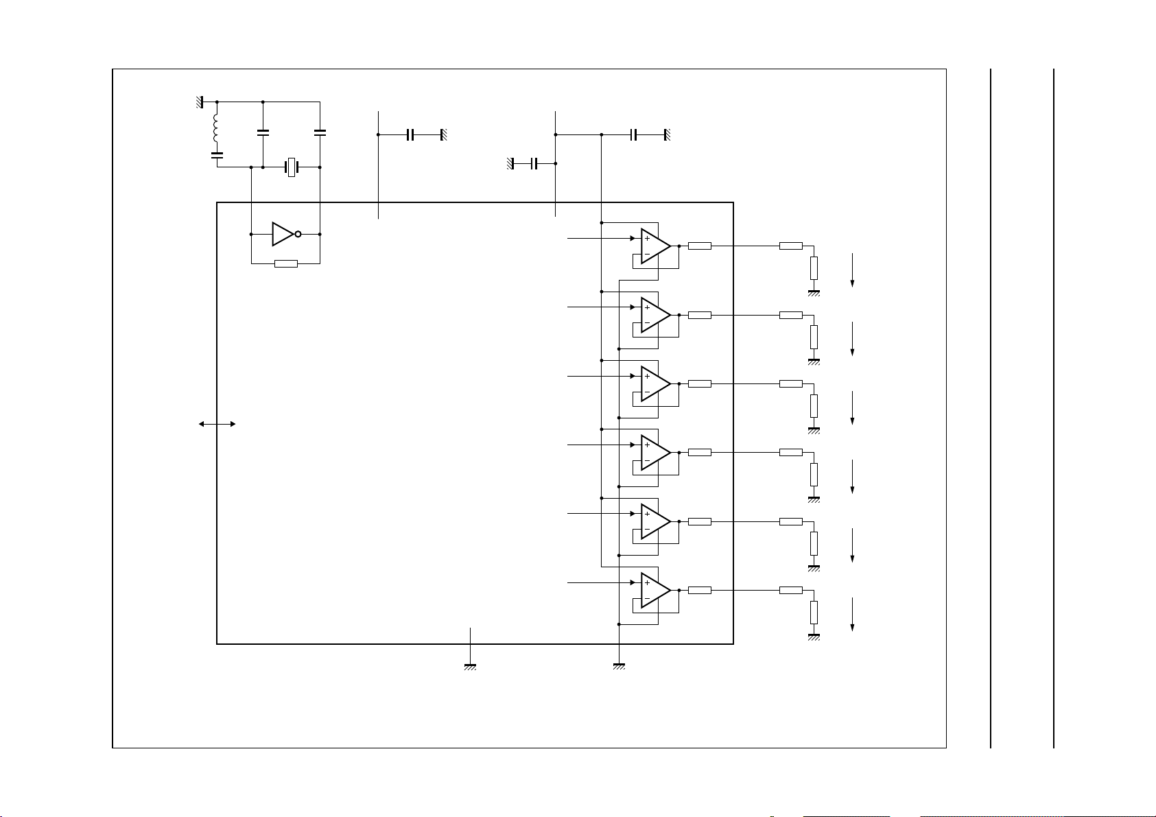
This text is here in white to force landscape pages to be rotated correctly when browsing through the pdf in the Acrobat reader.This text is here in
d
_white to force landscape pages to be rotated correctly when browsing through the pdf in the Acrobat reader.This text is here inThis text is here in
white to force landscape pages tobe rotated correctly when browsing through the pdf in the Acrobat reader. white to force landscape pages to be ...
2000 Mar 08 48
DGND
digital
inputs and
outputs
(1) Typical value.
100
(2) For
⁄
colour bar.
100
0.1 µH
1 nF
10 pF 10 pF
27.0 MHz
3rd harmonic
35 34
X1
XTALXTALI
+3.3 V digital
use one capacitor
for each V
V
DDD1
6, 17, 39
SAA7128H
SAA7129H
0.1 µF
to V
DGND
DDD
DDD3
DGND
book, full pagewidth
AGND
5, 18, 38
V
to V
SSD1
+3.3 V analog
0.1 µF
V
DDA4
DAC1
DAC2
DAC3
DAC4
DAC5
DAC6
SSD3
0.1 µF
use one capacitor
for each V
V
25, 28, 3136
AGND
DDA1
22, 32, 33
V
SSA1
to V
DDA
DDA3
to V
AGND
2 Ω
2 Ω
2 Ω
2 Ω
2 Ω
2 Ω
SSA3
(1)
30
CVBS
(1)
27
VBS
(1)
24
C
(1)
23
RED
(1)
26
GREEN
(1)
29
BLUE
4.7 Ω
10 Ω
10 Ω
23 Ω
23 Ω
23 Ω
75 Ω
AGND
75 Ω
AGND
75 Ω
AGND
75 Ω
AGND
75 Ω
AGND
75 Ω
AGND
U
CVBS
1.23 V (p-p)
U
VBS
1.00 V (p-p)
U
C
0.89 V (p-p)
U
R
0.70 V (p-p)
U
G
0.70 V (p-p)
U
B
0.70 V (p-p)
MHB583
9 APPLICATION INFORMATION
Philips Semiconductors Product specification
Digital video encoder SAA7128H; SAA7129H
(2)
(2)
(2)
(2)
(2)
(2)
Fig.24 Application circuit.
Page 49

Philips Semiconductors Product specification
Digital video encoder SAA7128H; SAA7129H
9.1 Analog output voltages
Theanalog outputvoltages are dependenton theopen-loopvoltage ofthe operational amplifiersfor full-scaleconversion
(typical value 1.375 V), the internal series resistor (typical value 2 Ω), the external series resistor and the external load
impedance.
The digital output signalsin frontof the DACs under nominal conditions occupydifferent conversionranges, asindicated
in Table 76 for a
Values for the external series resistors result in a 75 Ω load.
Table 76 Digital output signals conversion range
CVBS, SYNC TIP-TO-PEAK
CARRIER (digits)
100
⁄
colour bar signal.
100
CONVERSION RANGE (peak-to-peak)
Y (VBS)
SYNC TIP-TO-WHITE
(digits)
1016 881 712
BLACK-TO-WHITE AT GDY = GDC = −6 (digits)
RGB (Y)
2000 Mar 08 49
Page 50
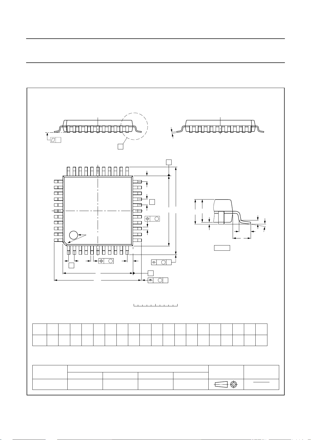
Philips Semiconductors Product specification
Digital video encoder SAA7128H; SAA7129H
10 PACKAGE OUTLINE
QFP44: plastic quad flat package; 44 leads (lead length 1.3 mm); body 10 x 10 x 1.75 mm
c
y
X
A
33 23
34
pin 1 index
44
1
22
Z
E
e
H
E
E
w M
b
p
12
11
A
2
A
A
1
detail X
SOT307-2
(A )
3
θ
L
p
L
w M
b
e
p
D
H
D
Z
D
B
0 2.5 5 mm
scale
DIMENSIONS (mm are the original dimensions)
mm
A
max.
2.10
0.25
0.05
1.85
1.65
0.25
UNIT A1A2A3b
cE
p
0.40
0.25
0.20
0.14
(1)
(1) (1)(1)
D
10.1
9.9
eH
10.1
9.9
12.9
0.8 1.3
12.3
Note
1. Plastic or metal protrusions of 0.25 mm maximum per side are not included.
OUTLINE
VERSION
IEC JEDEC EIAJ
REFERENCES
SOT307-2
2000 Mar 08 50
v M
H
v M
D
A
B
E
12.9
12.3
LL
p
0.95
0.55
0.15 0.10.15
EUROPEAN
PROJECTION
Z
D
1.2
0.8
Zywv θ
E
1.2
0.8
o
10
o
0
ISSUE DATE
95-02-04
97-08-01
Page 51

Philips Semiconductors Product specification
Digital video encoder SAA7128H; SAA7129H
11 SOLDERING
11.1 Introduction to soldering surface mount
packages
Thistext gives averybrief insight toa complex technology.
A more in-depth account of soldering ICs can be found in
our
“Data Handbook IC26; Integrated Circuit Packages”
(document order number 9398 652 90011).
There is no soldering method that is ideal for all surface
mount IC packages.Wave solderingis notalways suitable
for surface mount ICs, or for printed-circuit boards with
high population densities. In these situations reflow
soldering is often used.
11.2 Reflow soldering
Reflow soldering requires solder paste (a suspension of
fine solder particles, flux and binding agent) to be applied
tothe printed-circuitboardby screenprinting,stencilling or
pressure-syringe dispensing before package placement.
Several methods exist for reflowing; for example,
infrared/convection heating in a conveyor type oven.
Throughput times (preheating, soldering and cooling) vary
between 100 and 200 seconds depending on heating
method.
Typical reflow peak temperatures range from
215 to 250 °C. The top-surface temperature of the
packages should preferable be kept below 230 °C.
11.3 Wave soldering
Conventional single wave soldering is not recommended
forsurface mount devices(SMDs)or printed-circuit boards
with a high component density, as solder bridging and
non-wetting can present major problems.
To overcome these problems the double-wave soldering
method was specifically developed.
• Use a double-wave soldering method comprising a
turbulent wavewith high upwardpressure followed bya
smooth laminar wave.
• For packages with leads on two sides and a pitch (e):
– larger than or equal to 1.27 mm, the footprint
longitudinal axis is preferred to be parallel to the
transport direction of the printed-circuit board;
– smaller than 1.27 mm, the footprint longitudinal axis
must be parallel to the transport direction of the
printed-circuit board.
The footprint must incorporate solder thieves at the
downstream end.
• Forpackages with leadsonfour sides, thefootprintmust
be placedat a 45° angle to the transport direction of the
printed-circuit board. The footprint must incorporate
solder thieves downstream and at the side corners.
During placement and before soldering, the package must
be fixed with a droplet of adhesive. The adhesive can be
applied by screen printing, pin transfer or syringe
dispensing. The package can be soldered after the
adhesive is cured.
Typical dwell time is 4 seconds at 250 °C.
A mildly-activated flux will eliminate the need for removal
of corrosive residues in most applications.
11.4 Manual soldering
Fix the component by first soldering two
diagonally-opposite end leads. Use a low voltage (24 V or
less) soldering iron applied to the flat part of the lead.
Contact time must be limited to 10 seconds at up to
300 °C.
When using a dedicated tool, all other leads can be
soldered in one operation within 2 to 5 seconds between
270 and 320 °C.
If wave soldering is used the following conditions must be
observed for optimal results:
2000 Mar 08 51
Page 52

Philips Semiconductors Product specification
Digital video encoder SAA7128H; SAA7129H
11.5 Suitability of surface mount IC packages for wave and reflow soldering methods
PACKAGE
WAVE REFLOW
(1)
BGA, SQFP not suitable suitable
SOLDERING METHOD
HLQFP, HSQFP, HSOP, HTQFP, HTSSOP, SMS not suitable
(3)
PLCC
, SO, SOJ suitable suitable
LQFP, QFP, TQFP not recommended
SSOP, TSSOP, VSO not recommended
(2)
(3)(4)
(5)
suitable
suitable
suitable
Notes
1. All surface mount (SMD) packages are moisture sensitive. Depending upon the moisture content, the maximum
temperature (with respect to time) and body size of the package, there is a risk that internal or external package
cracks may occur due to vaporization of the moisture in them (the so called popcorn effect). For details, refer to the
Drypack information in the
“Data Handbook IC26; Integrated Circuit Packages; Section: Packing Methods”
.
2. These packages are not suitable for wave soldering as a solder joint between the printed-circuit board and heatsink
(at bottom version) can not be achieved, and as solder may stick to the heatsink (on top version).
3. If wave soldering is considered, then the package must be placed at a 45° angle to the solder wave direction.
The package footprint must incorporate solder thieves downstream and at the side corners.
4. Wave soldering is only suitable for LQFP, TQFP and QFP packages with a pitch (e) equal to or larger than 0.8 mm;
it is definitely not suitable for packages with a pitch (e) equal to or smaller than 0.65 mm.
5. Wave soldering isonly suitable for SSOP and TSSOP packageswith a pitch (e) equalto or larger than 0.65 mm; it is
definitely not suitable for packages with a pitch (e) equal to or smaller than 0.5 mm.
2000 Mar 08 52
Page 53
Philips Semiconductors Product specification
Digital video encoder SAA7128H; SAA7129H
12 DEFINITIONS
Data sheet status
Objective specification This data sheet contains target or goal specifications for product development.
Preliminary specification This data sheet contains preliminary data; supplementary data may be published later.
Product specification This data sheet contains final product specifications.
Limiting values
Limiting values given are in accordance with the Absolute Maximum Rating System (IEC 134). Stress above one or
more of the limiting values may cause permanent damage to the device. These are stress ratings only and operation
of the device at these or at any other conditions above those given in the Characteristics sections of the specification
is not implied. Exposure to limiting values for extended periods may affect device reliability.
Application information
Where application information is given, it is advisory and does not form part of the specification.
13 LIFE SUPPORT APPLICATIONS
These products are not designed for use in life support appliances, devices, or systems where malfunction of these
products can reasonably be expected to result in personal injury. Philips customers using or selling these products for
use in such applications do so at their own risk and agree to fully indemnify Philips for any damages resulting from such
improper use or sale.
14 PURCHASE OF PHILIPS I
Purchase of Philips I
components inthe I2C systemprovided the system conforms to the I2C specificationdefined by
Philips. This specification can be ordered using the code 9398 393 40011.
2
C COMPONENTS
2
C components conveys a license under the Philips’ I2C patent to use the
2000 Mar 08 53
Page 54

Philips Semiconductors Product specification
Digital video encoder SAA7128H; SAA7129H
NOTES
2000 Mar 08 54
Page 55

Philips Semiconductors Product specification
Digital video encoder SAA7128H; SAA7129H
NOTES
2000 Mar 08 55
Page 56

Philips Semiconductors – a w orldwide compan y
Argentina: see South America
Australia: 3 Figtree Drive, HOMEBUSH, NSW 2140,
Tel. +61 2 9704 8141, Fax. +61 2 9704 8139
Austria: Computerstr. 6, A-1101 WIEN, P.O. Box 213,
Tel. +43 1 60 101 1248, Fax. +43 1 60 101 1210
Belarus: Hotel Minsk Business Center, Bld. 3, r. 1211, Volodarski Str. 6,
220050 MINSK, Tel. +375 172 20 0733, Fax. +375 172 20 0773
Belgium: see The Netherlands
Brazil: see South America
Bulgaria: Philips Bulgaria Ltd., Energoproject, 15th floor,
51 James Bourchier Blvd., 1407 SOFIA,
Tel. +359 2 68 9211, Fax. +359 2 68 9102
Canada: PHILIPS SEMICONDUCTORS/COMPONENTS,
Tel. +1 800 234 7381, Fax. +1 800 943 0087
China/Hong Kong: 501 Hong Kong Industrial Technology Centre,
72 Tat Chee Avenue, Kowloon Tong, HONG KONG,
Tel. +852 2319 7888, Fax. +852 2319 7700
Colombia: see South America
Czech Republic: see Austria
Denmark: Sydhavnsgade 23, 1780 COPENHAGEN V,
Tel. +45 33 29 3333, Fax. +45 33 29 3905
Finland: Sinikalliontie 3, FIN-02630 ESPOO,
Tel. +358 9 615 800, Fax. +358 9 6158 0920
France: 51 Rue Carnot, BP317, 92156 SURESNES Cedex,
Tel. +33 1 4099 6161, Fax. +33 1 4099 6427
Germany: Hammerbrookstraße 69, D-20097 HAMBURG,
Tel. +49 40 2353 60, Fax. +49 40 2353 6300
Hungary: see Austria
India: Philips INDIA Ltd, Band Box Building, 2nd floor,
254-D, Dr. Annie Besant Road, Worli, MUMBAI 400 025,
Tel. +91 22 493 8541, Fax. +91 22 493 0966
Indonesia: PT Philips Development Corporation, Semiconductors Division,
Gedung Philips, Jl. Buncit Raya Kav.99-100, JAKARTA 12510,
Tel. +62 21 794 0040 ext. 2501, Fax. +62 21 794 0080
Ireland: Newstead, Clonskeagh, DUBLIN 14,
Tel. +353 1 7640 000, Fax. +353 1 7640 200
Israel: RAPAC Electronics, 7 Kehilat Saloniki St, PO Box 18053,
TEL AVIV 61180, Tel. +972 3 645 0444, Fax. +972 3 649 1007
Italy: PHILIPS SEMICONDUCTORS, Via Casati, 23 - 20052 MONZA (MI),
Tel. +39 039 203 6838, Fax +39 039 203 6800
Japan: Philips Bldg 13-37, Kohnan 2-chome, Minato-ku,
TOKYO 108-8507, Tel. +81 3 3740 5130, Fax. +81 3 3740 5057
Korea: Philips House, 260-199 Itaewon-dong, Yongsan-ku, SEOUL,
Tel. +82 2 709 1412, Fax. +82 2 709 1415
Malaysia: No. 76 Jalan Universiti, 46200 PETALING JAYA, SELANGOR,
Tel. +60 3 750 5214, Fax. +60 3 757 4880
Mexico: 5900 Gateway East, Suite 200, EL PASO, TEXAS 79905,
Tel. +9-5 800 234 7381, Fax +9-5 800 943 0087
Middle East: see Italy
Netherlands: Postbus 90050, 5600 PB EINDHOVEN, Bldg. VB,
Tel. +31 40 27 82785, Fax. +31 40 27 88399
New Zealand: 2 Wagener Place, C.P.O. Box 1041, AUCKLAND,
Tel. +64 9 849 4160, Fax. +64 9 849 7811
Norway: Box 1, Manglerud 0612, OSLO,
Tel. +47 22 74 8000, Fax. +47 22 74 8341
Pakistan: see Singapore
Philippines: Philips Semiconductors Philippines Inc.,
106 Valero St. Salcedo Village, P.O. Box 2108 MCC, MAKATI,
Metro MANILA, Tel. +63 2 816 6380, Fax. +63 2 817 3474
Poland: Al.Jerozolimskie 195 B, 02-222 WARSAW,
Tel. +48 22 5710 000, Fax. +48 22 5710 001
Portugal: see Spain
Romania: see Italy
Russia: Philips Russia, Ul. Usatcheva 35A, 119048 MOSCOW,
Tel. +7 095 755 6918, Fax. +7 095 755 6919
Singapore: Lorong 1, Toa Payoh, SINGAPORE 319762,
Tel. +65 350 2538, Fax. +65 251 6500
Slovakia: see Austria
Slovenia: see Italy
South Africa: S.A. PHILIPS Pty Ltd., 195-215 Main Road Martindale,
2092 JOHANNESBURG, P.O. Box 58088 Newville 2114,
Tel. +27 11 471 5401, Fax. +27 11 471 5398
South America: Al. Vicente Pinzon, 173, 6th floor,
04547-130 SÃO PAULO, SP, Brazil,
Tel. +55 11 821 2333, Fax. +55 11 821 2382
Spain: Balmes 22, 08007 BARCELONA,
Tel. +34 93 301 6312, Fax. +34 93 301 4107
Sweden: Kottbygatan 7, Akalla, S-16485 STOCKHOLM,
Tel. +46 8 5985 2000, Fax. +46 8 5985 2745
Switzerland: Allmendstrasse 140, CH-8027 ZÜRICH,
Tel. +41 1 488 2741 Fax. +41 1 488 3263
Taiwan: Philips Semiconductors, 6F, No. 96, Chien Kuo N. Rd., Sec. 1,
TAIPEI, Taiwan Tel. +886 2 2134 2886, Fax. +886 2 2134 2874
Thailand: PHILIPS ELECTRONICS (THAILAND) Ltd.,
209/2 Sanpavuth-Bangna Road Prakanong, BANGKOK 10260,
Tel. +66 2 745 4090, Fax. +66 2 398 0793
Turkey: Yukari Dudullu, Org. San. Blg., 2.Cad. Nr. 28 81260 Umraniye,
ISTANBUL, Tel. +90 216 522 1500, Fax. +90 216 522 1813
Ukraine: PHILIPS UKRAINE, 4 Patrice Lumumba str., Building B, Floor 7,
252042 KIEV, Tel. +380 44 264 2776, Fax. +380 44 268 0461
United Kingdom: Philips Semiconductors Ltd., 276 Bath Road, Hayes,
MIDDLESEX UB3 5BX, Tel. +44 208 730 5000, Fax. +44 208 754 8421
United States: 811 East Arques Avenue, SUNNYVALE, CA 94088-3409,
Tel. +1 800 234 7381, Fax. +1 800 943 0087
Uruguay: see South America
Vietnam: see Singapore
Yugoslavia: PHILIPS, Trg N. Pasica 5/v, 11000 BEOGRAD,
Tel. +381 11 3341 299, Fax.+381 11 3342 553
For all other countries apply to: Philips Semiconductors,
International Marketing & Sales Communications, Building BE-p, P.O. Box 218,
5600 MD EINDHOVEN, The Netherlands, Fax. +31 40 27 24825
© Philips Electronics N.V. SCA
All rights are reserved. Reproduction in whole or in part is prohibited without the prior written consent of the copyright owner.
The information presented in this document does not form part of any quotation or contract, is believed to be accurate and reliable and may be changed
without notice. No liability will be accepted by the publisher for any consequence of its use. Publication thereof does not convey nor imply any license
under patent- or other industrial or intellectual property rights.
2000
Internet: http://www.semiconductors.philips.com
69
Printed in The Netherlands 753505/01/pp56 Date of release: 2000 Mar 08 Document order number: 9397 750 06127
 Loading...