

Page 1
INTEGRATED CIRCUITS
DATA SH EET
SAA7114
PAL/NTSC/SECAM video decoder
with adaptive PAL/NTSC comb
filter, VBI data slicer and high
performance scaler
Product specification
Supersedes data of 2000 Mar 15
2004 Mar 03
Page 2

Philips Semiconductors Product specification
PAL/NTSC/SECAM video decoderwithadaptive PAL/NTSC
comb filter, VBI data slicer and high performance scaler
CONTENTS
1 FEATURES
1.1 Video decoder
1.2 Video scaler
1.3 Vertical Blanking Interval (VBI) data decoder
and slicer
1.4 Audio clock generation
1.5 Digital I/O interfaces
1.6 Miscellaneous
2 APPLICATIONS
3 GENERAL DESCRIPTION
4 QUICK REFERENCE DATA
5 ORDERING INFORMATION
6 BLOCK DIAGRAM
7 PINNING
8 FUNCTIONAL DESCRIPTION
8.1 Decoder
8.2 Decoder output formatter
8.3 Scaler
8.4 VBI data decoder and capture
(subaddresses 40H to 7FH)
8.5 Image port output formatter
(subaddresses 84H to 87H)
8.6 Audio clock generation
(subaddresses 30H to 3FH)
9 INPUT/OUTPUT INTERFACES AND PORTS
9.1 Analog terminals
9.2 Audio clock signals
9.3 Clock and real-time synchronization signals
9.4 Video expansion port (X port)
9.5 Image port (I port)
9.6 Host port for 16-bit extension ofvideodata I/O
(H port)
9.7 Basic input and output timing diagrams I port
and X port
10 BOUNDARY SCAN TEST
10.1 Initialization of boundary scan circuit
10.2 Device identification codes
11 LIMITING VALUES
12 THERMAL CHARACTERISTICS
13 CHARACTERISTICS
14 APPLICATION INFORMATION
15 I2C-BUS DESCRIPTION
15.1 I2C-bus format
15.2 I2C-bus details
15.3 Programming register audio clock generation
15.4 Programming register VBI data slicer
15.5 Programming register interfaces and scaler
part
16 PROGRAMMING START SET-UP
16.1 Decoder part
16.2 Audio clock generation part
16.3 Data slicer and data type control part
16.4 Scaler and interfaces
17 PACKAGE OUTLINES
18 SOLDERING
18.1 Introduction to soldering surface mount
packages
18.2 Reflow soldering
18.3 Wave soldering
18.4 Manual soldering
18.5 Suitability of surface mount IC packages for
wave and reflow soldering methods
19 DATA SHEET STATUS
20 DEFINITIONS
21 DISCLAIMERS
22 PURCHASE OF PHILIPS I2C COMPONENTS
SAA7114
2004 Mar 03 2
Page 3

Philips Semiconductors Product specification
PAL/NTSC/SECAM video decoder with adaptive PAL/NTSC
comb filter, VBI data slicer and high performance scaler
1 FEATURES
1.1 Video decoder
• Six analog inputs, internal analog source selectors, e.g.
6 × CVBS or (2 × Y/C and 2 × CVBS) or (1 × Y/C and
4 × CVBS)
• Two analog preprocessing channels in differential
CMOS style inclusive built-in analog anti-alias filters
• Fully programmable static gain or Automatic Gain
Control (AGC) for the selected CVBS or Y/C channel
• Automatic Clamp Control (ACC) for CVBS, Y and C
• Switchable white peak control
• Two 9-bit video CMOS Analog-to-Digital Converters
(ADCs), digitized CVBS or Y/C signals are available on
the expansion port
• On-chip line-locked clock generation in accordance with
“ITU 601”
• Digital PLL for synchronization and clock generation
from all standards and non-standard video sources e.g.
consumer grade VTR
• Requires only one crystal (32.11 or 24.576 MHz) for all
standards
• Horizontal and vertical sync detection
• Automatic detection of 50 and 60 Hz field frequency,
and automatic switching between PAL and NTSC
standards
• Luminance and chrominance signal processing for
PAL B, G, D, H, I and N, combination PAL N, PAL M,
NTSC M, NTSC-Japan, NTSC 4.43 and SECAM
• Adaptive 2/4-line comb filter for two dimensional
chrominance/luminance separation:
– Increasedluminanceandchrominancebandwidthfor
all PAL and NTSC standards
– Reduced cross colour and cross luminance artefacts
• PAL delay line for correcting PAL phase errors
• Independent Brightness Contrast Saturation (BCS)
adjustment for decoder part
• User programmable sharpness control
• Independent gain and offset adjustment for raw data
path.
1.2 Video scaler
• Horizontal and vertical downscaling and upscaling to
randomly sized windows
• Horizontal and vertical scaling range: variable zoom to
1
⁄64(icon) (it should be noted that the H and V zoom are
restricted by the transfer data rates)
• Anti-alias and accumulating filter for horizontal scaling
• Vertical scaling with linear phase interpolation and
accumulating filter for anti-aliasing (6-bit phase
accuracy)
• Horizontal phase correct up and downscaling for
improved signal quality of scaled data, especially for
compression and video phone applications, with 6-bit
phase accuracy (1.2 ns step width)
• Two independent programming sets for scaler part, to
define two ‘ranges’ per field or sequences over frames
• Fieldwise switching between decoder part and
expansion port (X port) input
• Brightness, contrast and saturation controls for scaled
outputs.
1.3 Vertical Blanking Interval (VBI) data decoder
and slicer
• Versatile VBI data decoder, slicer, clock regeneration
and byte synchronization e.g. for World Standard
Teletext(WST),NorthAmericanBroadcastTextSystem
(NABTS),closecaption,WideScreenSignalling(WSS),
etc.
1.4 Audio clock generation
• Generation of a field-locked audio master clock to
support a constant number of audio clocks per video
field
• Generation of an audio serial and left/right (channel)
clock signal.
SAA7114
2004 Mar 03 3
Page 4

Philips Semiconductors Product specification
PAL/NTSC/SECAM video decoder with adaptive PAL/NTSC
comb filter, VBI data slicer and high performance scaler
1.5 Digital I/O interfaces
• Real-time signal port (R port), inclusive continuous
line-locked reference clock and real-time status
information supporting RTC level 3.1 (refer to document
“RTC Functional Specification”
• Bidirectional expansion port (X port) with half duplex
functionality (D1), 8-bit Y-CB-CR:
– Output from decoder part, real-time and unscaled
– Input to scaler part, e.g. video from MPEG decoder
(extension to 16-bit possible)
• Video image port (I port) configurable for 8-bit data
(extension to 16-bit possible) in master mode (own
clock), or slave mode (external clock), with auxiliary
timing and handshake signals
• Discontinuous data streams supported
• 32-word × 4-byte FIFO register for video output data
• 28-word × 4-byte FIFO register for decoded VBI data
output
• Scaled 4:2:2, 4:1:1, 4:2:0, 4:1:0 Y-CB-C
output
• Scaled 8-bit luminance only and raw CVBS data output
• Sliced, decoded VBI data output.
1.6 Miscellaneous
• Power-on control
• 5 V tolerant digital inputs and I/O ports
• Software controlled power saving standby modes
supported
• Programming via serial I2C-bus, full read back ability by
an external controller, bit rate up to 400 kbits/s
• Boundary scan test circuit complies with the
1149.b1 - 1994”
2 APPLICATIONS
• Desktop video
• Multimedia
• Digital television
• Image processing
• Video phone applications.
.
for details)
R
“IEEE Std.
3 GENERAL DESCRIPTION
The SAA7114 is a video capture device for applications at
the image port of VGA controllers.
The SAA7114 is a combination of a two-channel analog
preprocessing circuit including source selection,
anti-aliasing filter and ADC, an automatic clamp and gain
control, a Clock Generation Circuit (CGC), a digital
multistandard decoder containing two-dimensional
chrominance/luminance separation by an adaptive comb
filter and a high performance scaler, including variable
horizontal and vertical up and downscaling and a
brightness, contrast and saturation control circuit.
It is a highly integrated circuit for desktop video and similar
applications. The decoder is based on the principle of
line-lockedclockdecodingandisabletodecode the colour
of PAL, SECAM and NTSC signals into ITU 601
compatible colour component values. The SAA7114
accepts CVBS or S-video (Y/C) as analog inputs from TV
or VCR sources, including weak and distorted signals.
An expansion port (X port) for digital video (bidirectional
halfduplex,D1 compatible) is also supported to connect to
MPEGor a video phone codec. Atthe so called image port
(I port) the SAA7114 supports 8 or 16-bit wide output data
with auxiliary reference data for interfacing to VGA
controllers.
The target application for the SAA7114 is to capture and
scale video images, to be provided as a digital video
stream through the image port of a VGA controller, for
display via the frame buffer of the VGA, or for capture to
system memory.
In parallel SAA7114 also incorporates provisions for
capturing the serially coded data in the vertical blanking
interval (VBI data). Two principal functions are available:
1. To capture raw video samples, after interpolation to
the required output data rate, via the scaler
2. A versatile data slicer (data recovery) unit.
The SAA7114 also incorporates field-locked audio clock
generation. This function ensures that there is always the
same number of audio samples associated with a field, or
a set of fields. This prevents the loss of synchronization
between video and audio during capture or playback.
The circuit is I2C-bus controlled (full write/read capability
for all programming registers, bit rate up to 400 kbits/s).
SAA7114
2004 Mar 03 4
Page 5
Philips Semiconductors Product specification
PAL/NTSC/SECAM video decoder with adaptive PAL/NTSC
SAA7114
comb filter, VBI data slicer and high performance scaler
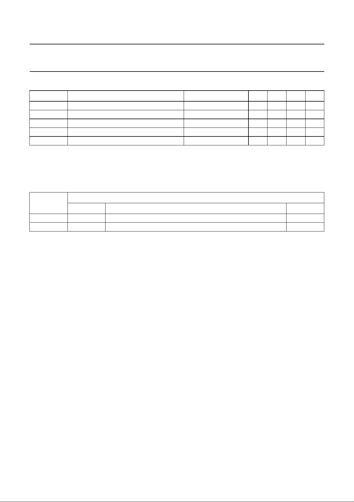
4 QUICK REFERENCE DATA
SYMBOL PARAMETER CONDITIONS MIN. TYP. MAX. UNIT
V
DDD
V
DDD(C)
V
DDA
T
amb
P
A+D
Note
1. Power dissipation is measured in CVBS input mode (only one ADC active) and 8-bit image port output mode,
expansion port is 3-stated.
5 ORDERING INFORMATION
TYPE
NUMBER
SAA7114E BGA156 plastic ball grid array package; 156 balls; body 15 × 15 × 1.15 mm SOT472-1
SAA7114H LQFP100 plastic low profile quad flat package; 100 leads; body 14 × 14 × 1.4 mm SOT407-1
digital supply voltage 3.0 3.3 3.6 V
digital core supply voltage 3.0 3.3 3.6 V
analog supply voltage 3.1 3.3 3.5 V
ambient temperature 0 − 70 °C
analog and digital power dissipation note 1 − 0.45 − W
PACKAGE
NAME DESCRIPTION VERSION
2004 Mar 03 5
Page 6
This text is here in white to force landscape pages to be rotated correctly when browsing through the pdf in the Acrobat reader.This text is here in
_white to force landscape pages to be rotated correctly when browsing through the pdf in the Acrobat reader.This text is here inThis text is here in
white to force landscape pages to be rotated correctly when browsing through the pdf in the Acrobat reader. white to force landscape pages to be ...
2004 Mar 03 6
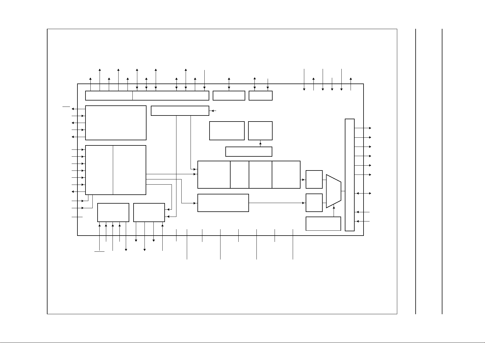
6 BLOCK DIAGRAM
Philips Semiconductors Product specification
PAL/NTSC/SECAM video decoder with adaptive PAL/NTSC
comb filter, VBI data slicer and high performance scaler
RES
CE
XTOUT
XTALI
XTALO
AI11
AI12
AI21
AI22
AI23
AI24
AOUT
AI1D
AI2D
AGND
LLC2
LLC
CLOCK GENERATION
POWER-ON CONTROL
ANALOG
DUAL
ADC
RTS0
RTCO
(1)
AND
BOUNDARY
SCAN
TEST
XCLK
RTS1
DIGITAL
DECODER
WITH
ADAPTIVE
COMB
FILTER
]
XPD[7:0
XDQ XRH
EXPANSION PORT PIN MAPPING I/O CONTROL I2C-BUSREAL-TIME OUTPUT
X-PORT I/O FORMATTING
AUDIO
CLOCK
GENERATION
XRV
XTRI
]
XRDY SDA SCL
FIR-PREFILTER
PRESCALER
SCALER BCS
GENERAL PURPOSE
HPD[7:0
chrominance of 16-bit input
PROGRAMMING
REGISTER
ARRAY
EVENT CONTROLLER
LINE
AND
VBI-DATA SLICER
FIFO
BUFFER
REGISTER
VERTICAL
SCALING
A/B
MUX
HORIZONTAL
FINE
(PHASE)
SCALING
TEST5
TEST4
SAA7114
VIDEO
FIFO
TEXT
FIFO
VIDEO/TEXT
TEST3
ARBITER
TEST2
32
to
8(16)
MUX
TEST1
TEST0
IMAGE PORT PIN MAPPING
MHC611
IPD[7:0
IDQ
IGPH
IGPV
IGP0
IGP1
ICLK
ITRDY
ITRI
]
TCK
TDI
AMCLK
TMS
TRST
(1) The pins RTCO and ALRCLK are used for configuration of the I2C-bus interface
and the definition of the crystal oscillator frequency at RESET (pin strapping).
ALRCLK
(1)
ASCLK
AMXCLKTDO
V
DD(XTAL)
V
SS(XTAL)
V
DDD(ICO1)
to
V
DDD(ICO6)
Fig.1 Block diagram.
V
DDD(EP1)
to
V
DDD(EP4)
V
DDA0
to
V
DDA2
V
V
handbook, full pagewidth
SSD(ICO1)
to
SSD(ICO3)
V
V
SSD(EP1)
to
SSD(EP4)
V
SSA0
V
SSA2
to
SAA7114
Page 7
Philips Semiconductors Product specification
PAL/NTSC/SECAM video decoder with adaptive PAL/NTSC
SAA7114
comb filter, VBI data slicer and high performance scaler
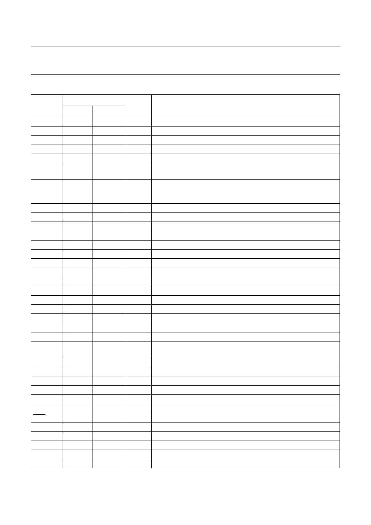
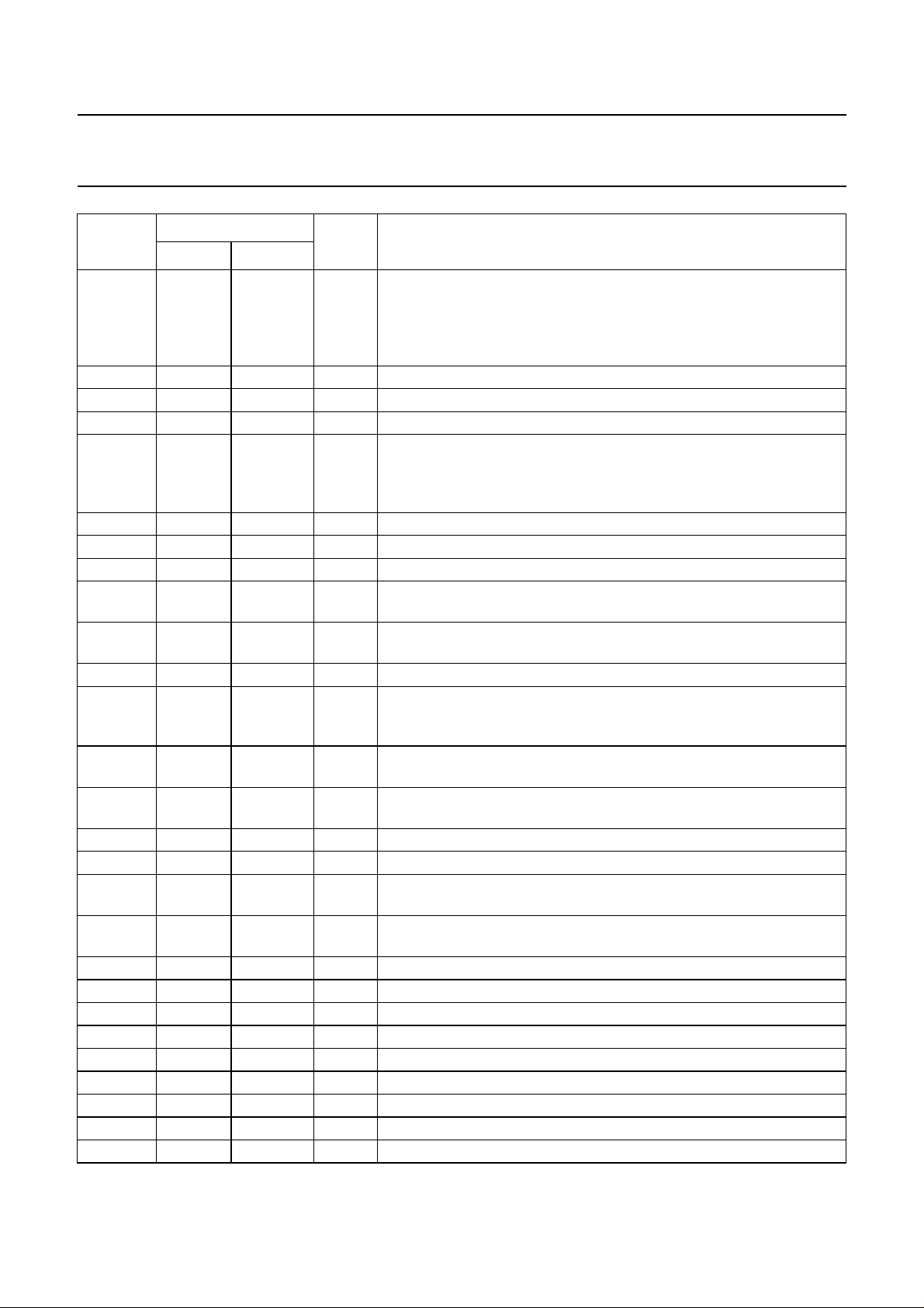
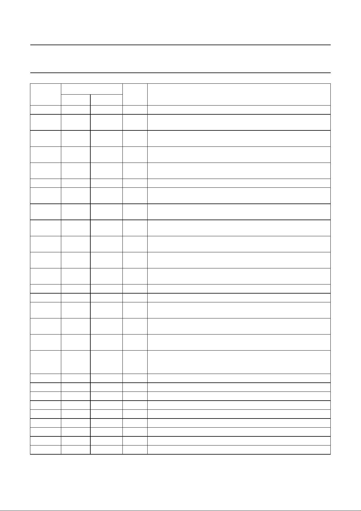
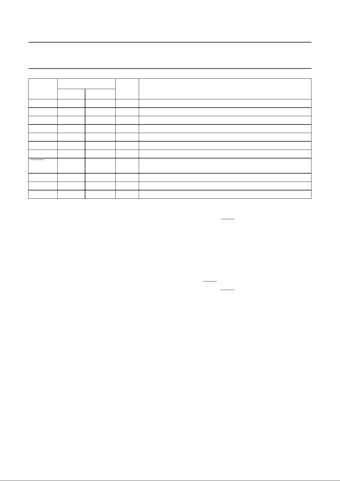
7 PINNING
SYMBOL
PIN
LQFP100 BGA156
V
DDD(EP1)
1 L7 P external digital pad supply voltage 1 (+3.3 V)
TDO 2 N5 O test data output for boundary scan test; note 2
TDI 3 N6 I/pu test data input for boundary scan test; note 2
XTOUT 4 P4 O crystal oscillator output signal; auxiliary signal
V
SS(XTAL)
5 P5 P ground for crystal oscillator
XTALO 6 P3 O 24.576 MHz (32.11 MHz) crystal oscillator output; not connected if TTL
XTALI 7 P2 I input terminal for 24.576 MHz (32.11 MHz) crystal oscillator or
V
DD(XTAL)
V
SSA2
8 L8 P supply voltage for crystal oscillator
9 M7, N7 P ground for analog inputs AI2n
AI24 10 P6 I analog input 24
V
DDA2
11 M8 P analog supply voltage for analog inputs AI2n (+3.3 V)
AI23 12 P7 I analog input 23
AI2D 13 P8 I differential input for ADC channel 2 (pins AI24, AI23, AI22 and AI21)
AI22 14 P9 I analog input 22
V
SSA1
15 N8, N9 P ground for analog inputs AI1n
AI21 16 P10 I analog input 21
V
DDA1
17 P analog supply voltage for analog inputs AI1n (+3.3 V)
AI12 18 P11 I analog input 12
AI1D 19 P12 I differential input for ADC channel 1 (pins AI12 and AI11)
AI11 20 P13 I analog input 11
AGND 21 N10 P analog ground connection
AOUT 22 M10 O do not connect; analog test output
V
DDA0
V
SSA0
V
DDD(EP2)
V
SSD(EP1)
23 N11 P analog supply voltage (+3.3 V) for internal Clock Generation Circuit
24 N12, N13 P ground for internal clock generation circuit
25 L9 P external digital pad supply voltage 2 (+3.3 V)
26 M13 P external digital pad supply ground 1
CE 27 N14 I/pu chip enable or reset input (with internal pull-up)
LLC 28 M14 O line-locked system clock output (27 MHz nominal)
LLC2 29 L14 O line-locked1⁄2clock output (13.5 MHz nominal)
RES 30 M12 O reset output (active LOW)
SCL 31 M11 I(/O) serial clock input (I2C-bus) with inactive output path
SDA 32 L12 I/O serial data input/output (I2C-bus)
V
DDD(ICO1)
33 L11 P internal digital core supply voltage 1 (+3.3 V)
RTS0 34 K13 O real-time status or sync information, controlled by subaddresses
RTS1 35 L10 O
TYPE
(1)
DESCRIPTION
clock input of XTALI is used
connection of external oscillator with TTL compatible square wave
clock signal
(CGC)
11H and 12H; see Section 15.2.18, 15.2.19 and 15.2.20
2004 Mar 03 7
Page 8
Philips Semiconductors Product specification
PAL/NTSC/SECAM video decoder with adaptive PAL/NTSC
SAA7114
comb filter, VBI data slicer and high performance scaler
SYMBOL
RTCO 36 L13 (I/)O real-time control output; contains information about actual system clock
AMCLK 37 K12 O audio master clock output, up to 50% of crystal clock
V
SSD(ICO1)
ASCLK 39 K14 O audio serial clock output
ALRCLK 40 J13 (I/)O audio left/right clock output; can be strapped to supply via a 3.3 kΩ
AMXCLK 41 J12 I audio master external clock input
ITRDY 42 J14 I/pu target ready input, image port (with internal pull-up)
V
DDD(ICO2)
TEST0 44 H13 O do not connect; reserved for future extensions and for testing: scan
ICLK 45 H12 I/O clock output signal for image port, or optional asynchronous back-end
IDQ 46 H14 O output data qualifier for image port (optional: gated clock output)
ITRI 47 G14 I(/O) image port output control signal, effects all input port pins inclusive
IGP0 48 F14 O general purpose output signal 0; image port (controlled by
IGP1 49 G13 O general purpose output signal 1; image port (controlled by
V
SSD(EP2)
V
DDD(EP3)
IGPV 52 F13 O multi purposevertical reference output signal; image port (controlled by
IGPH 53 G12 O multipurposehorizontalreference output signal; image port (controlled
IPD7 54 E14 O MSB of image port data output
IPD6 55 D14 O MSB − 1 of image port data output
IPD5 56 C14 O MSB − 2 of image port data output
IPD4 57 B14 O MSB − 3 of image port data output
V
DDD(ICO3)
IPD3 59 E13 O MSB − 4 of image port data output
IPD2 60 D13 O MSB − 5 of image port data output
IPD1 61 C13 O MSB − 6 of image port data output
IPD0 62 B13 O LSB of image port data output
LQFP100 BGA156
PIN
38 K11 P internal digital core supply ground 1
43 J11 P internal digital core supply voltage 2 (+3.3 V)
50 H11 P external digital pad supply ground 2
51 G11 P external digital pad supply voltage 3 (+3.3 V)
58 F11 P internal digital core supply voltage 3 (+3.3 V)
TYPE
(1)
frequency, field rate, odd/even sequence, decoder status, subcarrier
frequency and phase and PAL sequence (see external document
Functional Description”
via I2C-bus bit RTCE; see Table 36 and notes 3 and 4
resistor to indicate that the default 24.576 MHz crystal (ALRCLK = 0;
internal pull-down) has been replaced by a 32.110 MHz crystal
(ALRCLK = 1); notes 3 and 5
output
clock input
ICLK, enable and active polarity is under software control (bits IPE in
subaddress 87H); output path used for testing: scan output
subaddresses 84H and 85H)
subaddresses 84H and 85H)
subaddresses 84H and 85H)
by subaddresses 84H and 85H)
DESCRIPTION
, availableon request); the RTCOpin is enabled
“RTC
2004 Mar 03 8
Page 9
Philips Semiconductors Product specification
PAL/NTSC/SECAM video decoder with adaptive PAL/NTSC
SAA7114
comb filter, VBI data slicer and high performance scaler
SYMBOL
PIN
LQFP100 BGA156
V
SSD(ICO2)
63 E11 P internal digital core supply ground 2
HPD7 64 A13 I/O MSB of host port data I/O, carries CB-CR chrominance information in
HPD6 65 D12 I/O MSB − 1 of host port data I/O, carries CB-CR chrominance information
HPD5 66 C12 I/O MSB − 2 of host port data I/O, carries CB-CR chrominance information
HPD4 67 B12 I/O MSB − 3 of host port data I/O, carries CB-CR chrominance information
V
DDD(ICO4)
68 D11 P internal digital core supply voltage 4 (+3.3 V)
HPD3 69 A12 I/O MSB − 4 of host port data I/O, carries CB-CR chrominance information
HPD2 70 C11 I/O MSB − 5 of host port data I/O, carries CB-CR chrominance information
HPD1 71 B11 I/O MSB − 6 of host port data I/O, carries CB-CR chrominance information
HPD0 72 A11 I/O LSB of host port data I/O, carries CB-CR chrominance information in
TEST1 73 B10 I do not connect; reserved for future extensions and for testing: scan
TEST2 74 C10 I do not connect; reserved for future extensions and for testing: scan
V
DDD(EP4)
V
SSD(EP3)
75 D10 P external digital pad supply voltage 4 (+3.3 V)
76 H4 P external digital pad supply ground 3
TEST3 77 J3 I do not connect; reserved for future extensions and for testing: scan
TEST4 78 J1 O do not connect; reserved for future extensions and for testing: scan
TEST5 79 J2 I do not connect; reserved for future extensions and for testing: scan
XTRI 80 K1 I X port output control signal, affects all X port pins (XPD7 to XPD0,
XPD7 81 K2 I/O MSB of expansion port data
XPD6 82 K3 I/O MSB − 1 of expansion port data
V
DDD(ICO5)
83 J4 P internal digital core supply voltage 5 (+3.3 V)
XPD5 84 L1 I/O MSB − 2 of expansion port data
XPD4 85 L2 I/O MSB − 3 of expansion port data
XPD3 86 L3 I/O MSB − 4 of expansion port data
XPD2 87 M1 I/O MSB − 5 of expansion port data
V
SSD(ICO3)
88 K4 P internal digital core supply ground 3
XPD1 89 M2 I/O MSB − 6 of expansion port data
TYPE
(1)
DESCRIPTION
16-bit video I/O modes
in 16-bit video I/O modes
in 16-bit video I/O modes
in 16-bit video I/O modes
in 16-bit video I/O modes
in 16-bit video I/O modes
in 16-bit video I/O modes
16-bit video I/O modes
input
input
input
output
input
XRH, XRV, XDQ and XCLK), enable and active polarity is under
software control (bits XPE in subaddress 83H)
2004 Mar 03 9
Page 10
Philips Semiconductors Product specification
PAL/NTSC/SECAM video decoder with adaptive PAL/NTSC
SAA7114
comb filter, VBI data slicer and high performance scaler
SYMBOL
XPD0 90 N1 I/O LSB of expansion port data
XRV 91 L5 I/O vertical reference I/O expansion port
XRH 92 N2 I/O horizontal reference I/O expansion port
V
DDD(ICO6)
XCLK 94 M3 I/O clock I/O expansion port
XDQ 95 M4 I/O data qualifier I/O expansion port
XRDY 96 N3 O task flag or ready signal from scaler, controlled by XRQT
TRST 97 N4 I/pu test reset input (active LOW), for boundary scan test (with internal
TCK 98 M6 I/pu test clock for boundary scan test; note 2
TMS 99 M5 I/pu test mode select input for boundary scan test or scan test; note 2
V
SSD(EP4)
Notes
1. I = input, O = output, P = power, pu = pull-up.
2. In accordance with the
pull-up transistor and TDO is a 3-state output pad.
3. Pin strapping is done by connecting the pin to the supply via a 3.3 kΩ resistor. During the power-up reset sequence
the corresponding pins are switched to input mode to read the strapping level. For the default setting no strapping
resistor is necessary (internal pull-down).
4. Pin RTCO operates as I2C-bus slave address pin; RTCO = 0 slave address 42H/43H (default); RTCO = 1 slave
address 40H/41H.
5. Pin ALRCLK: 0 = 24.576 MHz crystal (default); 1 = 32.110 MHz crystal.
6. For board design without boundary scan implementation connect the TRST pin to ground.
7. This pin provides easy initialization of the Boundary Scan Test (BST) circuit. TRST can be used to force the Test
Access Port (TAP) controller to the TEST_LOGIC_RESET state (normal operation) at once.
LQFP100 BGA156
PIN
93 L4 P internal digital core supply voltage 6 (+3.3 V)
100 L6 P external digital pad supply ground 4
“IEEE1149.1”
(1)
TYPE
pull-up); notes 6 and 7
standard the pads TDI, TMS, TCK and TRST are input pads with an internal
DESCRIPTION
2004 Mar 03 10
Page 11
Philips Semiconductors Product specification
PAL/NTSC/SECAM video decoder with adaptive PAL/NTSC
comb filter, VBI data slicer and high performance scaler
V
DDD(EP1)
XTOUT
V
SS(XTAL)
XTALO
XTALI
V
DD(XTAL)
V
SSA2
V
DDA2
V
SSA1
V
DDA1
AGND
AOUT
V
DDA0
V
SSA0
V
DDD(EP2)
TDO
TDI
AI24
AI23
AI2D
AI22
AI21
AI12
AI1D
AI11
SSD(EP4)
V
TMS
TCK
XRDY
TRST
99989796959493929190898887868584838281
100
1
2
3
4
5
6
7
8
9
10
11
12
13
14
15
16
17
18
19
20
21
22
23
24
25
XDQ
XCLK
V
DDD(ICO6)
XRH
XRV
SSD(ICO3)
XPD0
XPD1
V
SAA7114H
XPD2
XPD3
XPD4
DDD(ICO5)
XPD5
V
XPD6
XPD7
XTRI
8079787776
TEST5
TEST4
SSD(EP3)
TEST3
V
SAA7114
V
75
DDD(EP4)
74
TEST2
73
TEST1
72
HPD0
71
HPD1
70
HPD2
69
HPD3
V
68
DDD(ICO4)
67
HPD4
66
HPD5
65
HPD6
64
HPD7
V
63
SSD(ICO2)
IPD0
62
61
IPD1
60
IPD2
59
IPD3
V
58
DDD(ICO3)
57
IPD4
56
IPD5
55
IPD6
54
IPD7
53
IGPH
52
IGPV
V
51
DDD(EP3)
26
CE
SSD(EP1)
V
LLC
31323334353637383940414243444546474849
SCL
RES
LLC2
SDA
DDD(ICO1)
V
RTS0
RTS1
RTCO
AMCLK
30
29
28
27
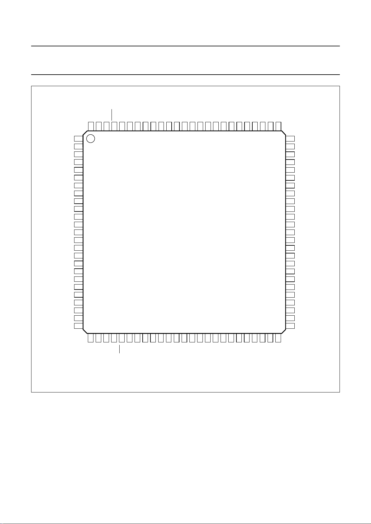
Fig.2 Pin configuration (LQFP100).
2004 Mar 03 11
ASCLK
SSD(ICO1)
V
ALRCLK
AMXCLK
ITRDY
DDD(ICO2)
V
ICLK
TEST0
IDQ
ITRI
IGP0
IGP1
V
50
MHB529
SSD(EP2)
Page 12
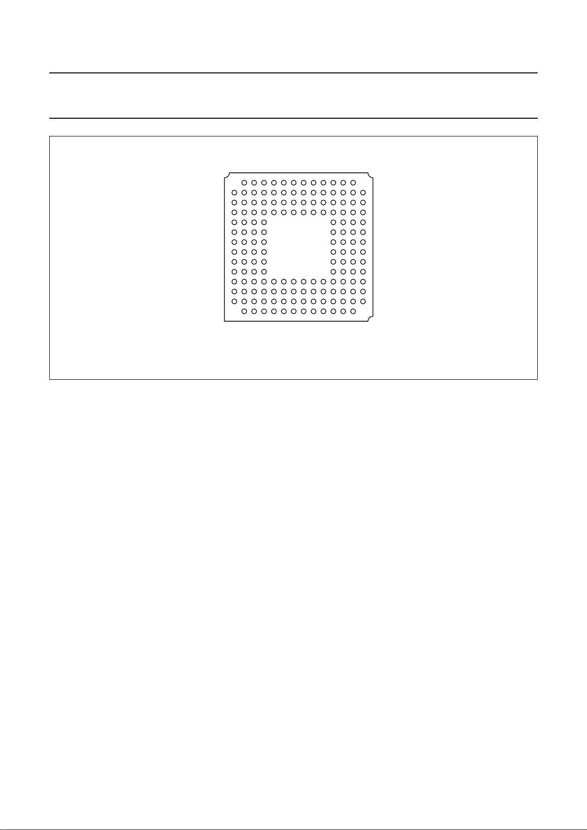
Philips Semiconductors Product specification
PAL/NTSC/SECAM video decoder with adaptive PAL/NTSC
comb filter, VBI data slicer and high performance scaler
handbook, halfpage
P
N
M
L
K
J
H
G
F
E
D
C
B
A
SAA7114E
1
234567891011121314
Fig.3 Pin configuration (BGA156).
MHC612
SAA7114
2004 Mar 03 12
Page 13
This text is here in white to force landscape pages to be rotated correctly when browsing through the pdf in the Acrobat reader.This text is here in
_white to force landscape pages to be rotated correctly when browsing through the pdf in the Acrobat reader.This text is here inThis text is here in
white to force landscape pages to be rotated correctly when browsing through the pdf in the Acrobat reader. white to force landscape pages to be ...
2004 Mar 03 13
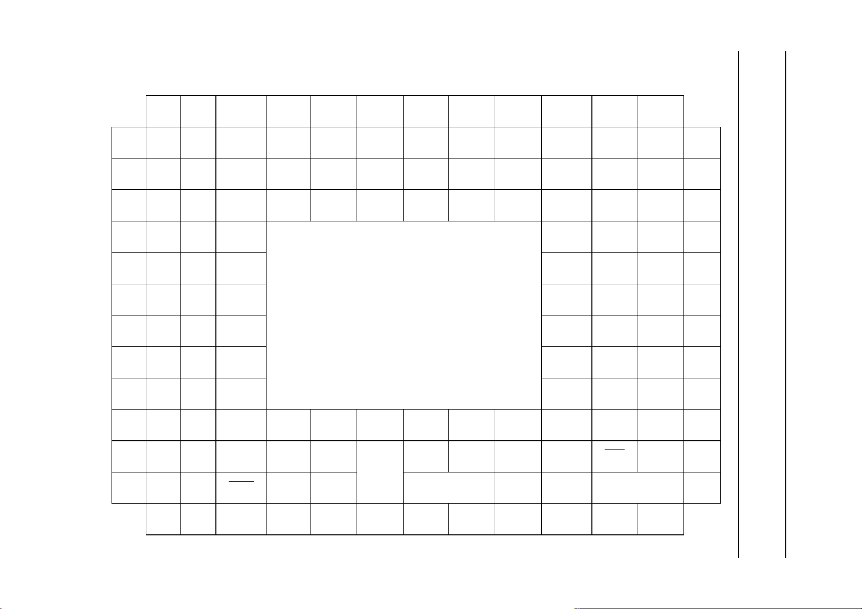
Table 1 Pin assignment (top view)
1 2 3 4 5 6 7 8 9 10 11 12 13 14
A n.c. n.c. n.c. n.c. n.c. n.c. n.c. n.c. n.c. HPD0 HPD3 HPD7
B n.c. n.c. n.c. n.c. n.c. n.c. n.c. n.c. n.c. TEST1 HPD1 HPD4 IPD0 IPD4
C n.c. n.c. n.c. n.c. n.c. n.c. n.c. n.c. n.c. TEST2 HPD2 HPD5 IPD1 IPD5
Philips Semiconductors Product specification
PAL/NTSC/SECAM video decoder with adaptive PAL/NTSC
comb filter, VBI data slicer and high performance scaler
D n.c. n.c. n.c. n.c. n.c. n.c. n.c. n.c. n.c. V
DDD(EP4)VDDD(ICO4)
E n.c. n.c. n.c. n.c. V
F n.c. n.c. n.c. n.c. V
G n.c. n.c. n.c. n.c. V
H n.c. n.c. n.c. V
J TEST4 TEST5 TEST3 V
K XTRI XPD7 XPD6 V
L XPD5 XPD4 XPD3 V
M XPD2 XPD1 XCLK XDQ TMS TCK V
N XPD0 XRH XRDY TRST TDO TDI V
SSD(EP3)
DDD(ICO5)
SSD(ICO3)
DDD(ICO6)
XRV V
SSD(EP4)VDDD(EP1)VDD(XTAL)VDDD(EP2)
SSA2
V
DDA2
SSA1
V
DDA1
V
V
RTS1 V
AOUT SCL RES V
AGND V
SSD(ICO2)
DDD(ICO3)
DDD(EP3)
V
SSD(EP2)
DDD(ICO2)
SSD(ICO1)
DDD(ICO1)
DDA0
HPD6 IPD2 IPD6
n.c. IPD3 IPD7
n.c. IGPV IGP0
IGPH IGP1 ITRI
ICLK TEST0 IDQ
AMXCLK ALRCLK ITRDY
AMCLK RTS0 ASCLK
SDA RTCO LLC2
LLC
CE
V
SSD(EP1)
SSA0
SAA7114
P XTALI XTALO XTOUT V
SS(XTAL)
AI24 AI23 AI2D AI22 AI21 AI12 AI1D AI11
Page 14

This text is here in white to force landscape pages to be rotated correctly when browsing through the pdf in the Acrobat reader.This text is here in
_white to force landscape pages to be rotated correctly when browsing through the pdf in the Acrobat reader.This text is here inThis text is here in
white to force landscape pages to be rotated correctly when browsing through the pdf in the Acrobat reader. white to force landscape pages to be ...
2004 Mar 03 14
Table 2 8-bit/16-bit and alternative pin function configurations
(1)
PIN
K2, K3,
L1 to L3,
M1, M2,
N1 (81,
82, 84 to
87, 89,
90)
M3 (94) XCLK clock
M4 (95) XDQ data
N3 (96) XRDY input
N2 (92) XRH horizontal
L5 (91) XRV vertical
K1 (80) XTRI output
SYMBOL
XPD7 to
XPD0
8-BIT
INPUT
MODES
D1 data
input
input
qualifier
input
ready
output
reference
input
reference
input
enable
input
16-BIT INPUT
MODES (ONLY
FOR I2C-BUS
PROGRAMMING)
Y data input D1
ALTERNATIVE
INPUT
FUNCTIONS
gated clock
input
active task A/B
flag
decoder
output
decoder
clock
output
data
qualifier
output
(HREFand
VREF
gate)
decoder
horizontal
reference
output
decoder
vertical
reference
output
8-BIT
OUTPUT
MODES
16-BIT OUTPUT
MODES (ONLY
FOR I2C-BUS
PROGRAMMING)
ALTERNATIVE
OUTPUT
FUNCTIONS
CONFIGURATION
PROGRAMMING
XCODE[92H[3]]
XPE[1:0] 83H[1:0]
+ pin XTRI
XPE[1:0] 83H[1:0]
+ pin XTRI
XPCK[1:0] 83H[5:4]
XCKS[92H[0]]
XDQ[92H[1]]
XPE[1:0] 83H[1:0]
+ pin XTRI
XRQT[83H[2]]
XPE[1:0] 83H[1:0]
+ pin XTRI
XDH[92H[2]]
XPE[1:0] 83H[1:0]
+ pin XTRI
XDV[1:0] 92H[5:4]
XPE[1:0] 83H[1:0]
+ pin XTRI
XPE[1:0] 83H[1:0]
I/O
BITS
Philips Semiconductors Product specification
PAL/NTSC/SECAM video decoder with adaptive PAL/NTSC
comb filter, VBI data slicer and high performance scaler
SAA7114
Page 15

This text is here in white to force landscape pages to be rotated correctly when browsing through the pdf in the Acrobat reader.This text is here in
_white to force landscape pages to be rotated correctly when browsing through the pdf in the Acrobat reader.This text is here inThis text is here in
white to force landscape pages to be rotated correctly when browsing through the pdf in the Acrobat reader. white to force landscape pages to be ...
2004 Mar 03 15
(1)
PIN
A13,
D12,
C12,
B12,
A12,
C11,
B11,A11
(64to 67,
69 to 72)
E14,
D14,
C14,
B14,
E13,
D13,
C13,B13
(54to 57,
59 to 62)
H12 (45) ICLK clock
H14 (46) IDQ data
J14 (42) ITRDY target
G12 (53) IGPH H gate
F13 (52) IGPV V gate
SYMBOL
HPD7 to
HPD0
IPD7 to
IPD0
8-BIT
INPUT
MODES
16-BIT INPUT
MODES (ONLY
FOR I2C-BUS
PROGRAMMING)
CB-CR data input CB-CR scaler
ALTERNATIVE
INPUT
FUNCTIONS
8-BIT
OUTPUT
MODES
D1 scaler
output
output
qualifier
output
ready input
output
output
16-BIT OUTPUT
MODES (ONLY
FOR I2C-BUS
PROGRAMMING)
output
Y scaler output ICODE[93H[7]]
ALTERNATIVE
OUTPUT
FUNCTIONS
clock input ICKS[1:0] 80H[1:0]
gated clock
output
extended
H gate,
horizontal
pulses
V-sync, vertical
pulses
CONFIGURATION
PROGRAMMING
ICODE[93H[7]]
ISWP[1:0] 85H[7:6]
I8_16[93H[6]]
IPE[1:0] 87H[1:0]
+ pin ITRI
ISWP[1:0] 85H[7:6]
I8_16[93H[6]]
IPE[1:0] 87H[1:0]
+ pin ITRI
IPE[1:0] 87H[1:0]
+ pin ITRI
ICKS[3:2] 80H[3:2]
IDQP[85H[0]]
IPE[1:0] 87H[1:0]
+ pin ITRI
IDH[1:0] 84H[1:0]
IRHP[85H[1]]
IPE[1:0] 87H[1:0]
+ pin ITRI
IDV[1:0] 84H[3:2]
IRVP[85H[2]]
IPE[1:0] 87H[1:0]
+ pin ITRI
I/O
BITS
Philips Semiconductors Product specification
PAL/NTSC/SECAM video decoder with adaptive PAL/NTSC
comb filter, VBI data slicer and high performance scaler
SAA7114
Page 16

This text is here in white to force landscape pages to be rotated correctly when browsing through the pdf in the Acrobat reader.This text is here in
_white to force landscape pages to be rotated correctly when browsing through the pdf in the Acrobat reader.This text is here inThis text is here in
white to force landscape pages to be rotated correctly when browsing through the pdf in the Acrobat reader. white to force landscape pages to be ...
2004 Mar 03 16
(1)
PIN
G13 (49) IGP1 general
F14 (48) IGP0 general
G14 (47) ITRI output
Note
1. Pin numbers for LQFP100 in parenthesis.
SYMBOL
8-BIT
INPUT
MODES
16-BIT INPUT
MODES (ONLY
FOR I2C-BUS
PROGRAMMING)
ALTERNATIVE
INPUT
FUNCTIONS
8-BIT
OUTPUT
MODES
purpose
purpose
enable
input
16-BIT OUTPUT
MODES (ONLY
FOR I2C-BUS
PROGRAMMING)
ALTERNATIVE
OUTPUT
FUNCTIONS
CONFIGURATION
PROGRAMMING
IDG1[1:0] 84H[5:4]
IG1P[85H[3]]
IPE[1:0] 87H[1:0]
+ pin ITRI
IDG0[1:0] 84H[7:6]
IG0P[85H[4]]
IPE[1:0] 87H[1:0]
+ pin ITRI
I/O
BITS
Philips Semiconductors Product specification
PAL/NTSC/SECAM video decoder with adaptive PAL/NTSC
comb filter, VBI data slicer and high performance scaler
SAA7114
Page 17
Philips Semiconductors Product specification
PAL/NTSC/SECAM video decoder with adaptive PAL/NTSC
comb filter, VBI data slicer and high performance scaler
8 FUNCTIONAL DESCRIPTION
8.1 Decoder
8.1.1 ANALOG INPUT PROCESSING
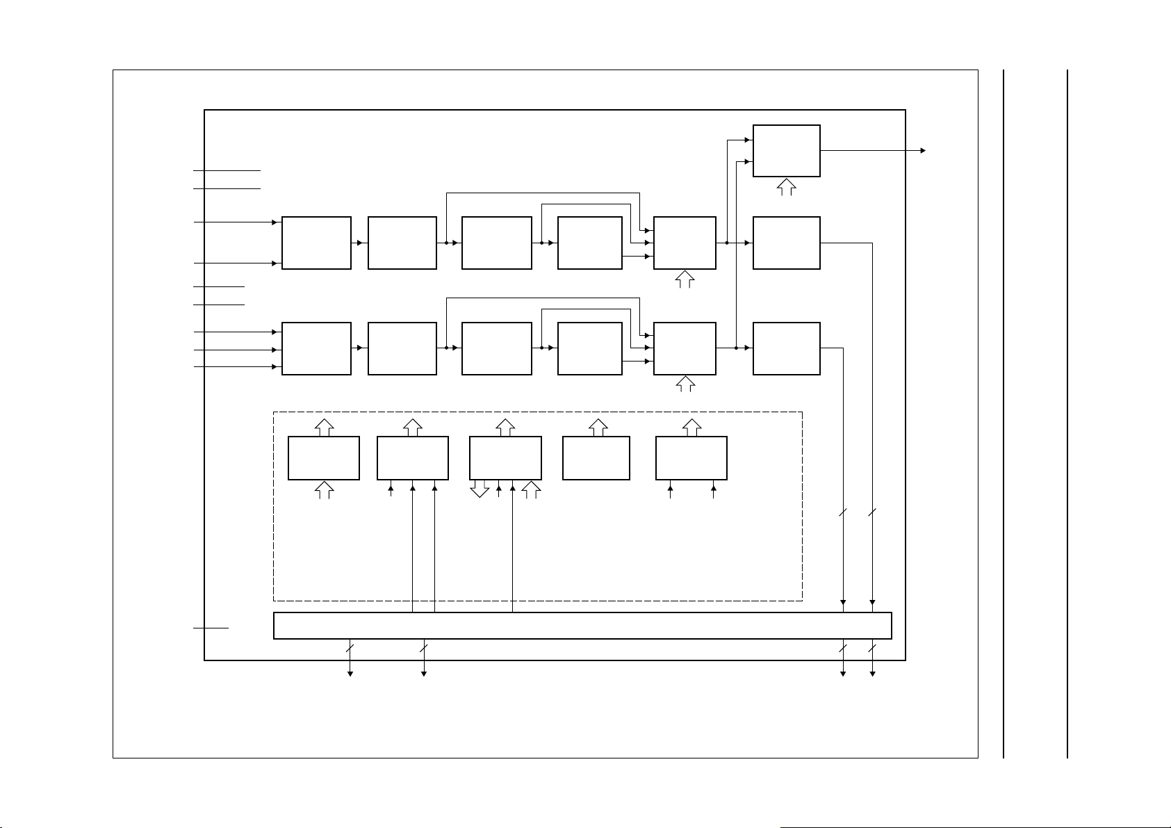
The SAA7114 offers six analog signal inputs, two analog
main channels with source switch, clamp circuit, analog
amplifier, anti-alias filter and video 9-bit CMOS ADC;
see Fig.7.
6
V
(dB)
0
−6
−12
8.1.2 ANALOG CONTROL CIRCUITS
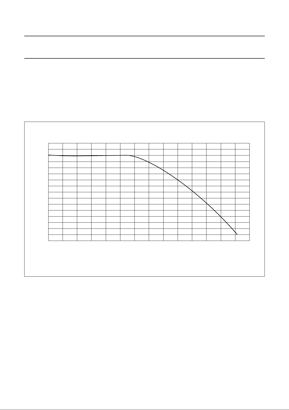
The anti-alias filters are adapted to the line-locked clock
frequency via a filter control circuit. The characteristic is
shown in Fig.4. During the vertical blanking period gain
and clamping control are frozen.
SAA7114
MGD138
−18
−24
−30
−36
−42
024 68101214
f (MHz)
Fig.4 Anti-alias filter.
2004 Mar 03 17
Page 18
Philips Semiconductors Product specification
PAL/NTSC/SECAM video decoder with adaptive PAL/NTSC
comb filter, VBI data slicer and high performance scaler
8.1.2.1 Clamping
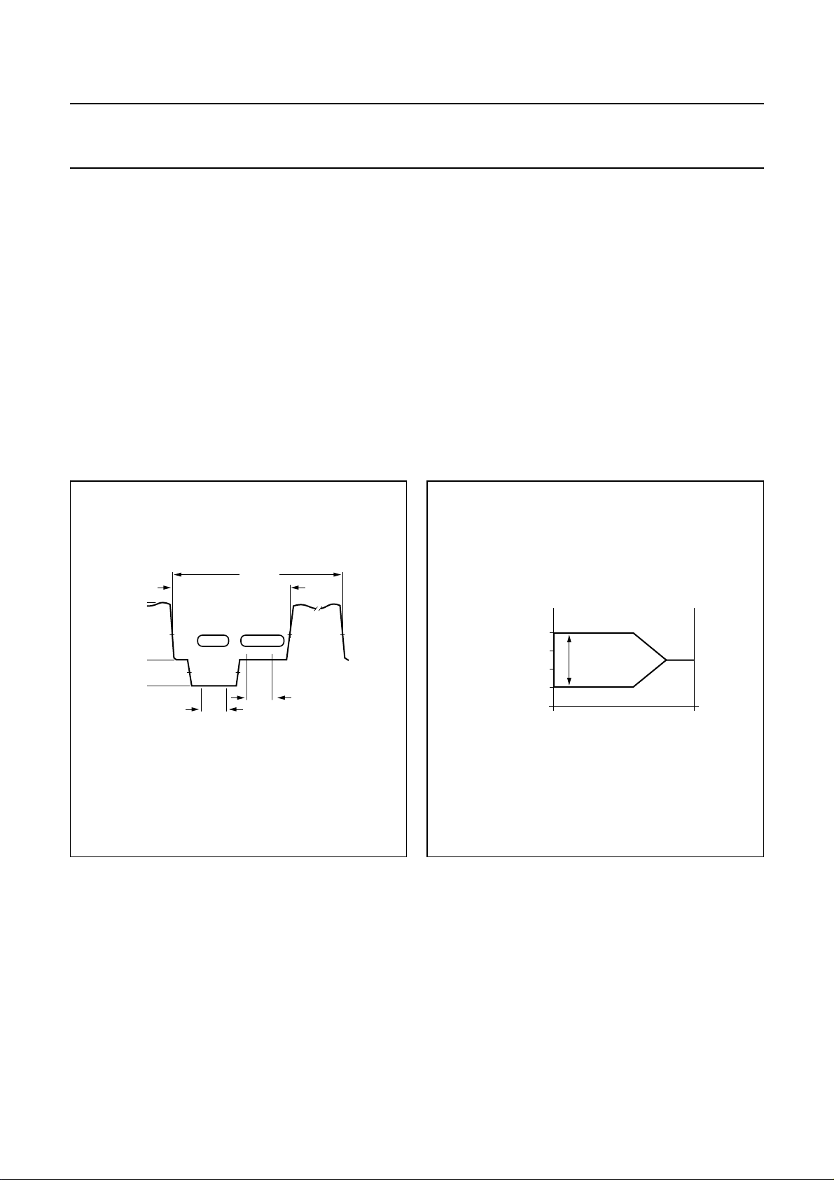
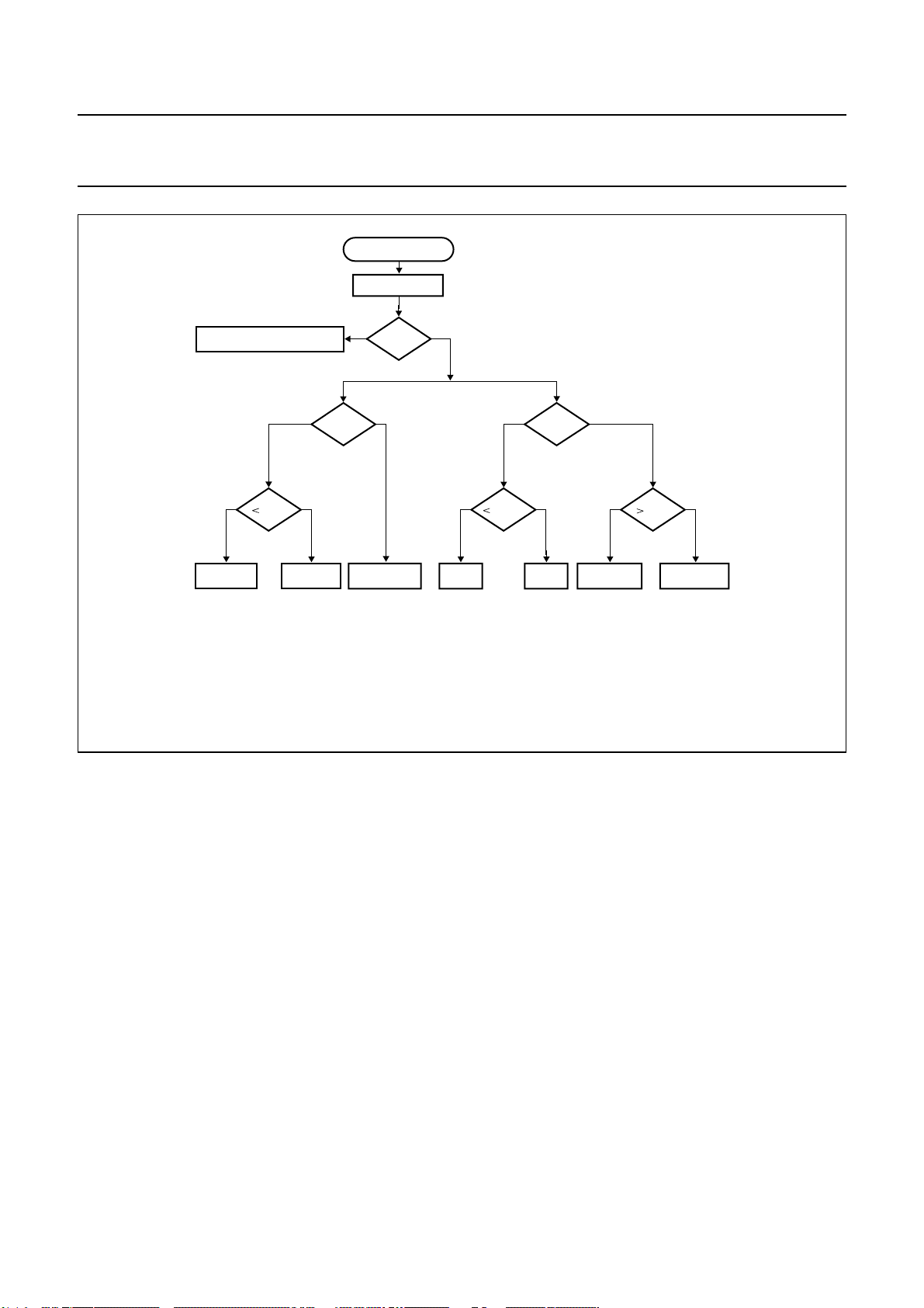
The clamp control circuit controls the correct clamping of
the analog input signals. The coupling capacitor is also
used to store and filter the clamping voltage. An internal
digital clamp comparator generates the information with
respect to clamp-up or clamp-down. The clamping levels
for the two ADC channels are fixed for luminance (60) and
chrominance (128). Clamping time in normal use is set
with the HCL pulse on the back porch of the video signal.
8.1.2.2 Gain control
The gain control circuit receives (via the I2C-bus) the static
gain levels for the two analog amplifiers or controls one of
theseamplifiersautomaticallyviaabuilt-inAutomaticGain
Control (AGC) as part of the Analog Input Control (AICO).
The AGC (automatic gain control for luminance) is used to
amplify a CVBS or Y signal to the required signal
amplitude, matched to the ADCs input voltage range. The
AGC active time is the sync bottom of the video signal.
Signal (white) peak control limits the gain at signal
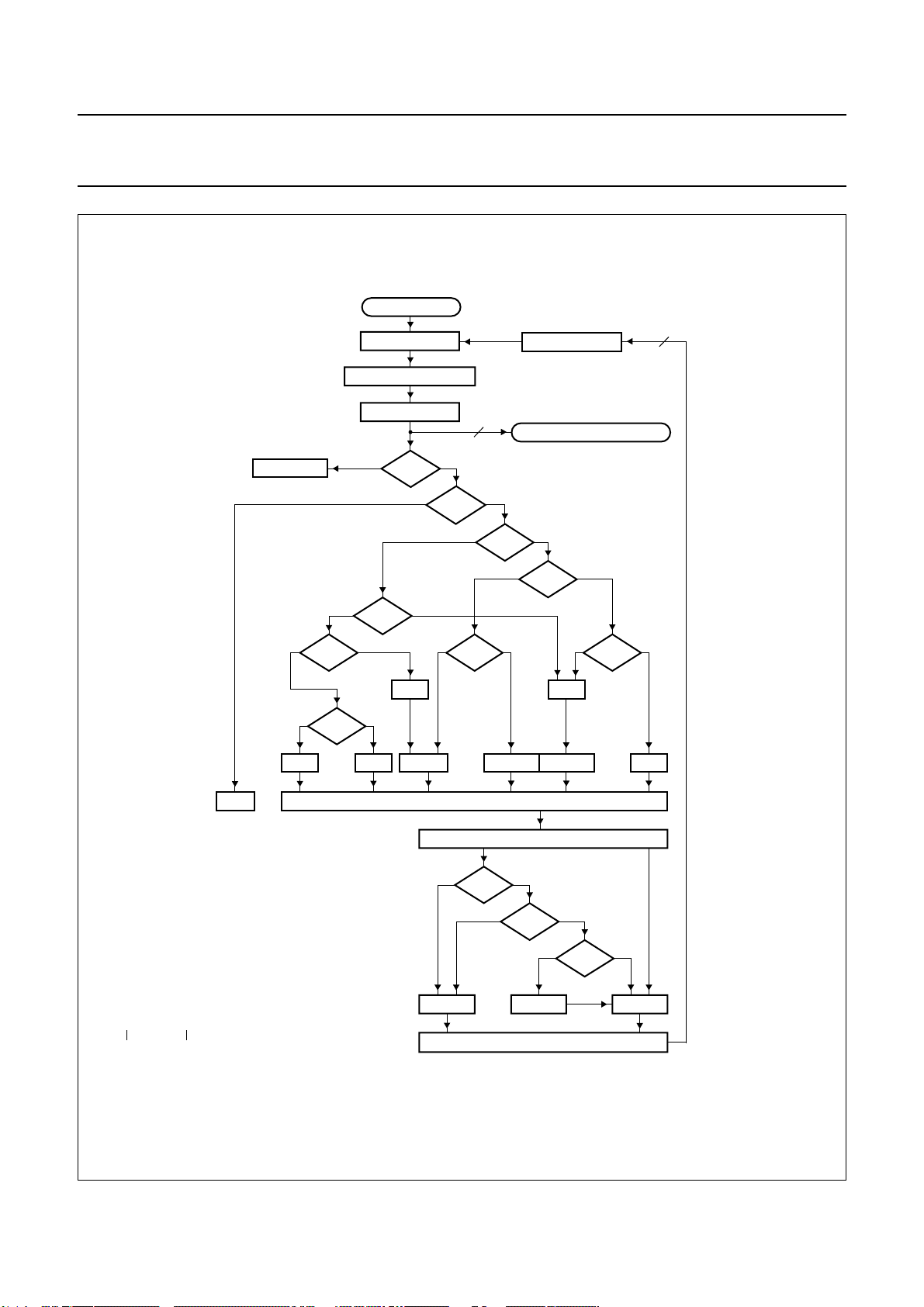
overshoots.Theflow charts (see Figs 8 and 9) show more
details of the AGC. The influence of supply voltage
variation within the specified range is automatically
eliminated by clamp and automatic gain control.
SAA7114
HSY
TV line
HCL
MGL065
analog line blanking
255
GAIN CLAMP
60
1
Fig.5 Analog line with clamp (HCL) and gain
range (HSY).
analog input level
+3 dB
0 dB
(1 V (p-p) 18/56 Ω)
−6 dB
Fig.6 Automatic gain range.
maximum
range 9 dB
minimum
controlled
ADC input level
0 dB
MHB325
2004 Mar 03 18
Page 19
This text is here in white to force landscape pages to be rotated correctly when browsing through the pdf in the Acrobat reader.This text is here in
_white to force landscape pages to be rotated correctly when browsing through the pdf in the Acrobat reader.This text is here inThis text is here in
white to force landscape pages to be rotated correctly when browsing through the pdf in the Acrobat reader. white to force landscape pages to be ...
2004 Mar 03 19
Philips Semiconductors Product specification
PAL/NTSC/SECAM video decoder with adaptive PAL/NTSC
comb filter, VBI data slicer and high performance scaler
V
SSA1
V
SSA2
AI2D
AI24 to AI21
V
DDA1
V
DDA2
AI12
AI1D
AI11
(15) N8, N9
(9) N7, N7
(13) P8
(10, 12, 14, 16)
P6, P7, P9, P10
(17) M9
(11) M8
(18) P11
(19) P12
(20) P13
SOURCE
SWITCH
SOURCE
SWITCH
MODE
CONTROL
MODE[3:0]
CLAMP
CIRCUIT
CLAMP
CIRCUIT
CLAMP
CONTROL
HCL
ANALOG
AMPLIFIER
ANALOG
AMPLIFIER
GLIMB
GLIMT
WIPA
SLTCA
DAC9
DAC9
GAIN
CONTROL
HSY
HOLDG
GAFIX
WPOFF
GUDL[1:0]
GAI[28:20]
GAI[18:10]
HLNRS
UPTCV
ANTI-ALIAS
FILTER
ANTI-ALIAS
FILTER
ANTI-ALIAS
CONTROL
BYPASS
SWITCH
BYPASS
SWITCH
FUSE[1:0
VERTICAL
BLANKING
CONTROL
VBLNK
SVREF
]
]
FUSE[1:0
VBSL
ANALOG CONTROL
TEST
SELECTOR
AND
BUFFER
AOSL[1:0
ADC2
ADC1
]
M10 (22)
99
AOUT
AGND
(21) N10
CROSS MULTIPLEXER
CVBS/CHRCVBS/LUM
Fig.7 Analog input processing using the SAA7114 as differential front-end with 9-bit ADC.
AD2BYP
9999
AD1BYP
mhc613
SAA7114
Page 20
Philips Semiconductors Product specification
PAL/NTSC/SECAM video decoder with adaptive PAL/NTSC
comb filter, VBI data slicer and high performance scaler
handbook, full pagewidth
NO ACTION
ANALOG INPUT
AMPLIFIER
ANTI-ALIAS FILTER
ADC
1
VBLK
1
0
HOLDG
gain
9
0
1
X
1
DAC
LUMA/CHROMA DECODER
0
0
HSY
SAA7114
9
STOP
X = system variable.
Y AGV FGV– GUDL>=
GUDL = gain update level (adjustable).
VBLK = vertical blanking pulse.
HSY = horizontal sync pulse.
AGV = actual gain value.
FGV = frozen gain value.
.
1
+1/F
0
10
<
4
>
496
+1/L
1
>
510
10
<
1
X = 0
0
1
X
+1/LLC2 −1/LLC2
1
GAIN VALUE 9-BIT
−1/LLC2
GAIN ACCUMULATOR (18 BITS)
ACTUAL GAIN VALUE 9-BIT (AGV) [−3/+6 dB
AGV
0
HSY
UPDATE
10
>
510
X = 1
+/− 0
0
1
0
Y
FGV
MHB728
]
Fig.8 Gain flow chart.
2004 Mar 03 20
Page 21
Philips Semiconductors Product specification
PAL/NTSC/SECAM video decoder with adaptive PAL/NTSC
comb filter, VBI data slicer and high performance scaler
ANALOG INPUT
ADC
NO BLANKING ACTIVE
10
+ CLAMP − CLAMP
WIPE = white peak level (254).
SBOT = sync bottom level (1).
CLL = clamp level [60 Y (128 C)].
HSY = horizontal sync pulse.
HCL = horizontal clamp pulse.
10 10
CLL
10
VBLK
GAIN -><- CLAMP
HCL HSY
01 10
SBOT
NO CLAMP
+ GAIN − GAIN
WIPE
fast − GAIN
SAA7114
slow + GAIN
MGC647
Fig.9 Clamp and gain flow chart.
2004 Mar 03 21
Page 22
This text is here in white to force landscape pages to be rotated correctly when browsing through the pdf in the Acrobat reader.This text is here in
n
_white to force landscape pages to be rotated correctly when browsing through the pdf in the Acrobat reader.This text is here inThis text is here in
white to force landscape pages to be rotated correctly when browsing through the pdf in the Acrobat reader. white to force landscape pages to be ...
2004 Mar 03 22
CVBS-IN
or Y-IN
LDEL
YCOMB
DELAY
COMPENSATION
QUADRATURE
MODULATOR
CB-C
CHR
R
dbook, full pagewidth
SUBTRACTOR
INTERPOLATION
LOW-PASS 3
LUBW
CB-C
Y
LUMINANCE-PEAKING
Y-DELAY ADJUSTMENT
LUFI[3:0
CSTD[2:0
R
YDEL[2:0
OR
LOW-PASS,
]
SET_RAW
]
SET_VBI
]
Y/CVBS
DBRI[7:0
DCON[7:0
DSAT[7:0
RAWG[7:0
RAWO[7:0
COLO
]
]
]
]
]
8.1.3 CHROMINANCE AND LUMINANCE PROCESSING
Philips Semiconductors Product specification
PAL/NTSC/SECAM video decoder with adaptive PAL/NTSC
comb filter, VBI data slicer and high performance scaler
CVBS-IN
or CHR-IN
QUADRATURE
DEMODULATOR
SUBCARRIER
GENERATION 1
HUEC
SUBCARRIER
GENERATION 2
CHROMINANCE
INCREMENT
DELAY
RTCO
LOW-PASS 1
DOWNSAMPLING
LCBW[2:0
LDEL
YCOMB
CHROMINANCE
INCREMENT
DTO RESET
SUBCARRIER
INCREMENT
GENERATION
AND
DIVIDER
CDTO
CSTD[2:0
INCS
]
ADAPTIVE
COMB FILTER
SET_RAW
]
SET_VBI
CGAIN[6:0
IDEL[3:0
CCOMB
YCOMB
PHASE
DEMODULATOR
AMPLITUDE
DETECTOR
BURST GATE
ACCUMULATOR
LOOP FILTER
FCTC
ACGC
]
]
LDEL
BYPS
CODE
CB-C
LOW-PASS 2
R
SECAM
PROCESSING
CHROMA
GAIN
CONTROL
CB-C
ADJUSTMENT
SECS
CHBW
R
fH/2 switch signal
BRIGHTNESS
CONTRAST
SATURATION
CONTROL
RAW DATA
GAIN AND
OFFSET
CONTROL
CB-C
R
PAL DELAY LINE
SECAM
RECOMBINATION
SET_RAW
SET_VBI
Y-OUT/
CVBS OUT
CB-CR-OUT
HREF-OUT
SET_RAW
SET_VBI
DCVF
MHB729
SAA7114
Fig.10 Chrominance and luminance processing.
Page 23

Philips Semiconductors Product specification
PAL/NTSC/SECAM video decoder with adaptive PAL/NTSC
comb filter, VBI data slicer and high performance scaler
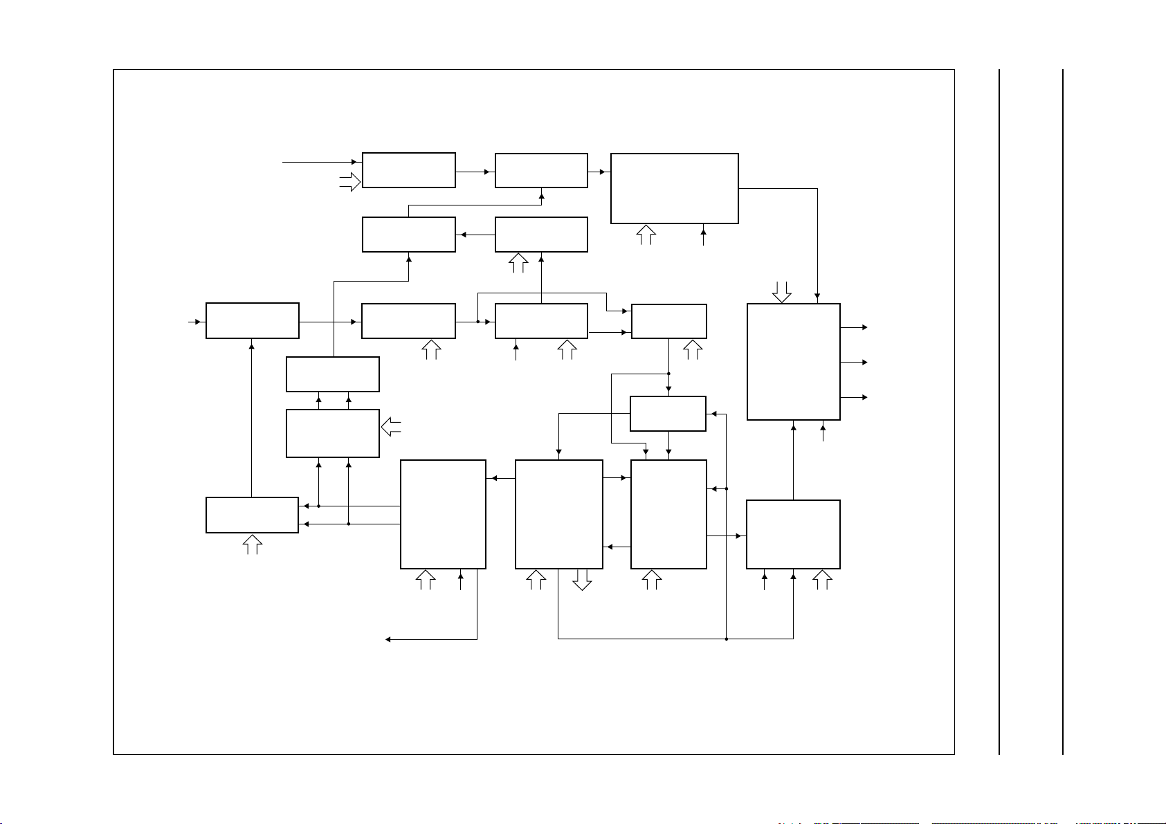
8.1.3.1 Chrominance path
The 9-bit CVBS or chrominance input signal is fed to the
inputofa quadrature demodulator, where it is multiplied by
twotime-multiplexed subcarrier signalsfromthe subcarrier
generation block 1 (0° and 90° phase relationship to the
demodulator axis). The frequency is dependent on the
chosen colour standard.
The time-multiplexed output signals of the multipliers are
low-pass filtered (low-pass 1). Eight characteristics are
programmable via LCWB3 to LCWB0 to achieve the
desired bandwidth for the colour difference signals (PAL,
NTSC) or the 0° and 90° FM signals (SECAM).
Thechrominance low-pass 1characteristicalso influences
the grade of cross-luminance reduction during horizontal
colour transients (large chrominance bandwidth means
strong suppression of cross-luminance). If the Y-comb
filterisdisabledbyYCOMB = 0thefilterinfluencesdirectly
the width of the chrominance notch within the luminance
path (a large chrominance bandwidth means wide
chrominance notch resulting in a lower luminance
bandwidth).
The low-pass filtered signals are fed to the adaptive comb
filter block. The chrominance components are separated
from the luminance via a two-line vertical stage (four lines
for PAL standards) and a decision logic between the
filtered and the non-filtered output signals. This block is
bypassed for SECAM signals. The comb filter logic can be
enabled independently for the succeeding luminance and
chrominance processing by YCOMB (subaddress 09H,
bit D6) and/or CCOMB (subaddress 0EH, bit D0). It is
always bypassed during VBI or raw data lines
programmable by the LCRn registers (subaddresses
41H to 57H); see Section 8.2.
The separated CB-CR components are further processed
by a second filter stage (low-pass 2) to modify the
chrominance bandwidth without influencing the luminance
path. Its characteristic is controlled by CHBW
(subaddress 10H, bit D3). For the complete transfer
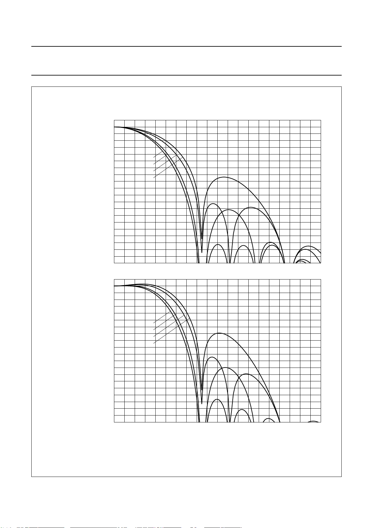
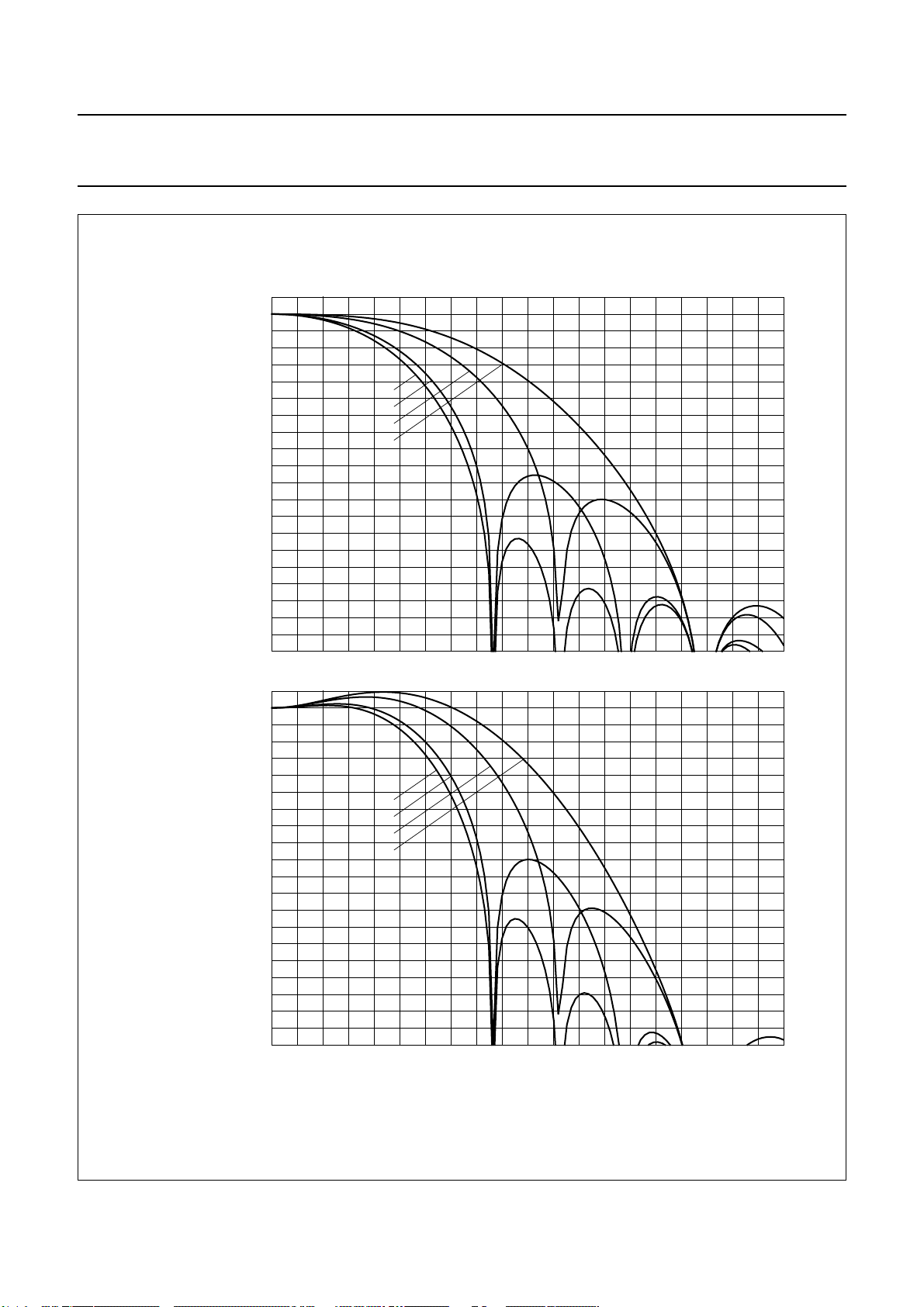
characteristic of low-passes 1 and 2 see Figs 11 and 12.
The succeeding chrominance gain control block amplifies
or attenuates the CB-CR signal according to the required
ITU 601/656 levels. It is controlled by the output signal
from the amplitude detection circuit within the burst
processing block.
The burst processing block provides the feedback loop of
the chrominance PLL and contains the following:
• Burst gate accumulator
• Colour identification and colour killer
• Comparisonnominal/actual burstamplitude(PAL/NTSC
standards only)
• Loop filter chrominance gain control (PAL/NTSC
standards only)
• Loop filter chrominance PLL (only active for PAL/NTSC
standards)
• PAL/SECAM sequence detection, H/2-switch
generation.
The increment generation circuit produces the Discrete
Time Oscillator (DTO) increment for both subcarrier
generation blocks. It contains a division by the increment
of the line-locked clock generator to create a stable
phase-locked sine signal under all conditions (e.g. for
non-standard signals).
The PAL delay line block eliminates crosstalk between the
chrominance channels in accordance with the PAL
standard requirements. For NTSC colour standards the
delay line can be used as an additional vertical filter.
If desired, it can be switched off by DCVF = 1. It is always
disabledduringVBIor raw data lines programmable by the
LCRn registers (subaddresses 41H to 57H); see
Section 8.2. The embedded line delay is also used for
SECAM recombination (cross-over switches).
SAA7114
The SECAM processing (bypassed for QAM standards)
contains the following blocks:
• Baseband ‘bell’ filters to reconstruct the amplitude and
phase equalized 0° and 90° FM signals
• Phase demodulator and differentiator
(FM-demodulation)
• De-emphasis filter to compensate the pre-emphasized
input signal, including frequency offset compensation
(DB or DR white carrier values are subtracted from the
signal, controlled by the SECAM switch signal).
2004 Mar 03 23
Page 24
Philips Semiconductors Product specification
PAL/NTSC/SECAM video decoder with adaptive PAL/NTSC
comb filter, VBI data slicer and high performance scaler
3
V
0
(dB)
−3
−6
−9
(1) LCBW[2:0] = 000.
(2) LCBW[2:0] = 010.
(3) LCBW[2:0] = 100.
(4) LCBW[2:0] = 110.
(5) LCBW[2:0] = 001.
(6) LCBW[2:0] = 011.
(7) LCBW[2:0] = 101.
(8) LCBW[2:0] = 111.
−12
−15
−18
−21
−24
−27
−30
−33
−36
−39
−42
−45
−48
−51
−54
−57
−60
0 0.2 0.4 0.6 0.8 1.0 1.2 1.4 1.6 1.8 2.0 2.2 2.4 2.6 2.8 3.0 3.2 3.4 3.6 3.8 4.0
3
V
0
(dB)
−3
−6
−9
−12
−15
−18
−21
−24
−27
−30
−33
−36
−39
−42
−45
−48
−51
−54
−57
−60
0 0.2 0.4 0.6 0.8 1.0 1.2 1.4 1.6 1.8 2.0 2.2 2.4 2.6 2.8 3.0 3.2 3.4 3.6 3.8 4.0
(1)
(2)
(3)
(4)
(5)
(6)
(7)
(8)
SAA7114
MHB533
f (MHz)
f (MHz)
Fig.11 Transfer characteristics of the chrominance low-pass at CHBW = 0.
2004 Mar 03 24
Page 25
Philips Semiconductors Product specification
PAL/NTSC/SECAM video decoder with adaptive PAL/NTSC
comb filter, VBI data slicer and high performance scaler
3
V
0
(dB)
−3
−6
−9
(1) LCBW[2:0] = 000.
(2) LCBW[2:0] = 010.
(3) LCBW[2:0] = 100.
(4) LCBW[2:0] = 110.
(5) LCBW[2:0] = 001.
(6) LCBW[2:0] = 011.
(7) LCBW[2:0] = 101.
(8) LCBW[2:0] = 111.
−12
−15
−18
−21
−24
−27
−30
−33
−36
−39
−42
−45
−48
−51
−54
−57
−60
0 0.2 0.4 0.6 0.8 1.0 1.2 1.4 1.6 1.8 2.0 2.2 2.4 2.6 2.8 3.0 3.2 3.4 3.6 3.8 4.0
3
V
0
(dB)
−3
−6
−9
−12
−15
−18
−21
−24
−27
−30
−33
−36
−39
−42
−45
−48
−51
−54
−57
−60
0 0.2 0.4 0.6 0.8 1.0 1.2 1.4 1.6 1.8 2.0 2.2 2.4 2.6 2.8 3.0 3.2 3.4 3.6 3.8 4.0
(1)
(2)
(3)
(4)
(5)
(6)
(7)
(8)
SAA7114
MHB534
f (MHz)
f (MHz)
Fig.12 Transfer characteristics of the chrominance low-pass at CHBW = 1.
2004 Mar 03 25
Page 26

Philips Semiconductors Product specification
PAL/NTSC/SECAM video decoder with adaptive PAL/NTSC
comb filter, VBI data slicer and high performance scaler
8.1.3.2 Luminance path
The rejection of the chrominance components within the
9-bit CVBS or Y input signal is achieved by subtracting the
remodulated chrominance signal from the CVBS input.
The comb filtered CB-CR components are interpolated
(upsampled) by the low-pass 3 block. Its characteristic is
controlled by LUBW (subaddress 09H, bit D4) to modify
the width of the chrominance ‘notch’ without influencing
the chrominance path. The programmable frequency
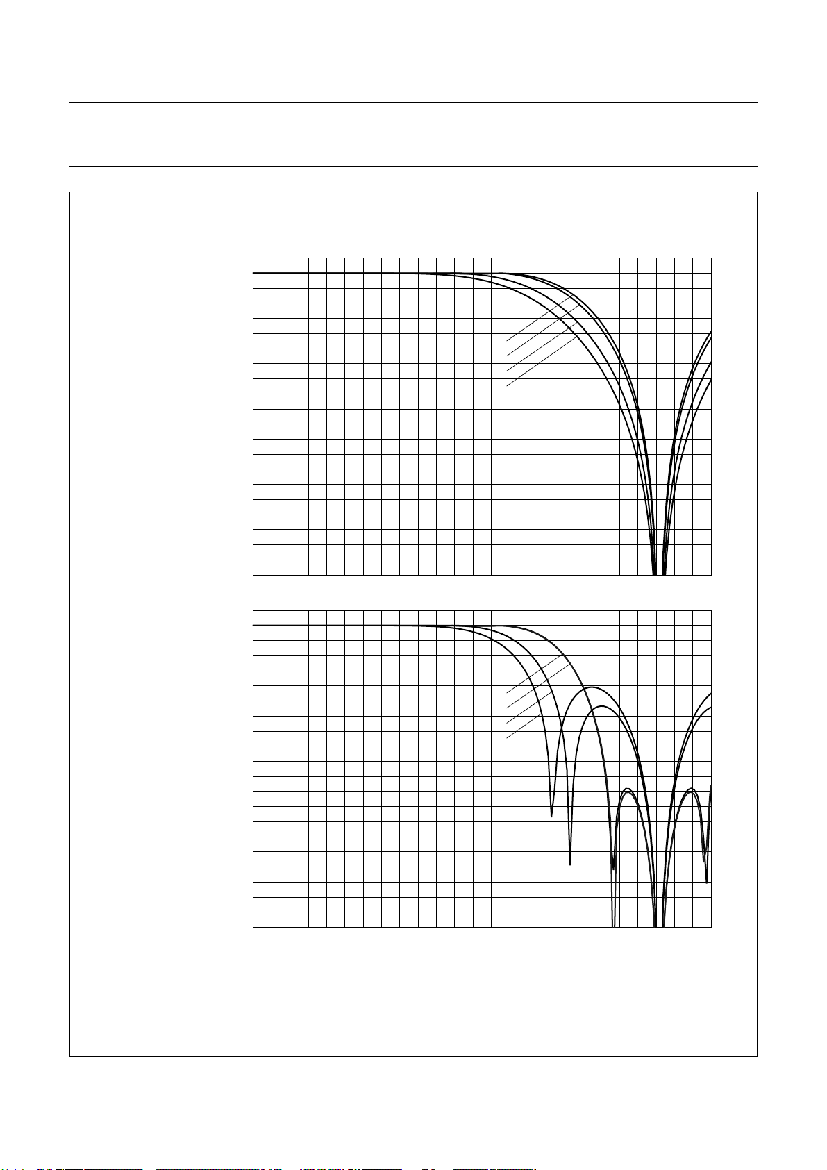
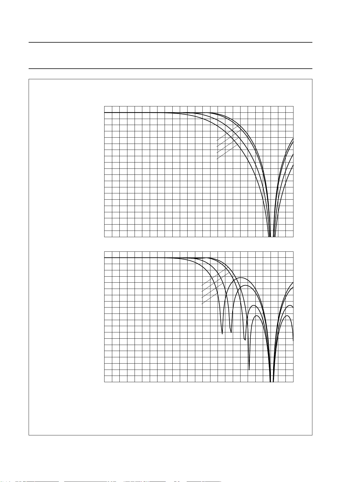
characteristicsavailable,inconjunctionwiththeLCBW2to
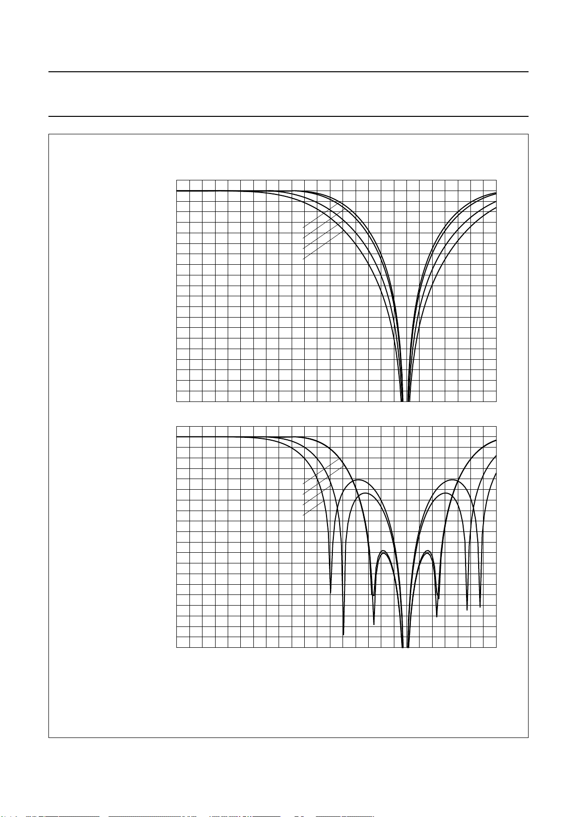
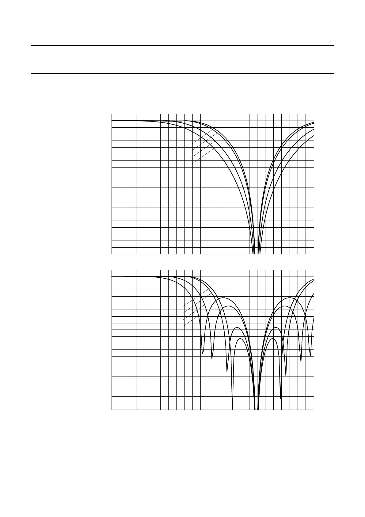
LCBW0settings,canbe seen in Figs 13 to 16. It should be
noted that these frequency curves are only valid for
Y-comb disabled filter mode (YCOMB = 0). In comb filter
modethe frequency response is flat. The centre frequency
of the notch is automatically adapted to the chosen colour
standard.
The interpolated CB-CR samples are multiplied by two
time-multiplexed subcarrier signals from the subcarrier
generation block 2. This second DTO is locked to the first
subcarrier generator by an increment delay circuit
matchedtotheprocessingdelay, which is different for PAL
and NTSC standards according to the chosen comb filter
algorithm. The two modulated signals are finally added to
build the remodulated chrominance signal.
The frequency characteristic of the separated luminance
signal can be further modified by the succeeding
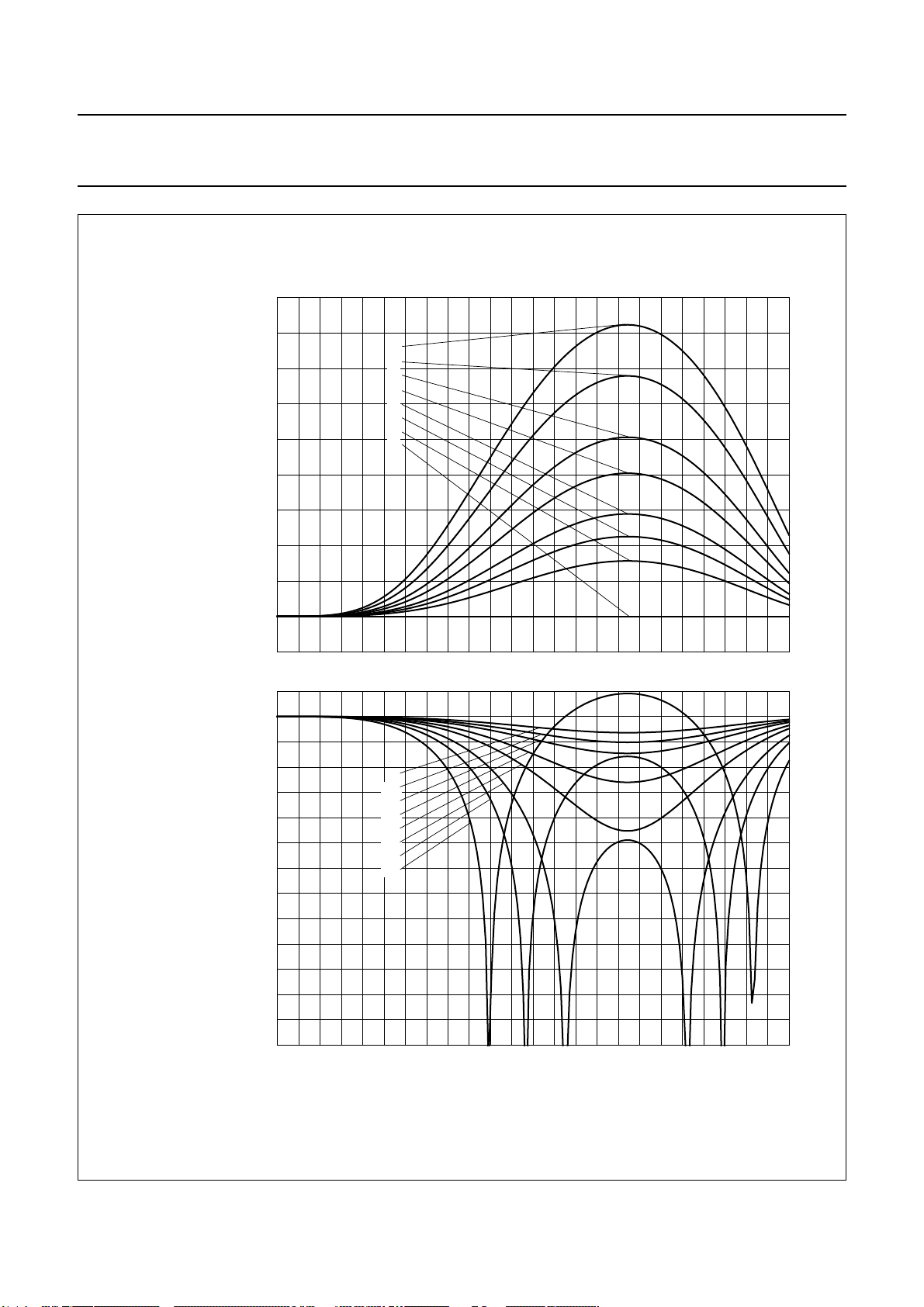
luminance filter block. It can be configured as peaking
(resolution enhancement) or low-pass block by LUFI3 to
LUFI0 (subaddress 09H, bits D3 to D0). The 16 resulting
frequency characteristics can be seen in Fig.17. The
LUFI3 to LUFI0 settings can be used as a user
programmable sharpness control.
The luminance filter block also contains the adjustable
Y-delay part; programmable by YDEL2 to YDEL0
(subaddress 11H, bits D2 to D0).
SAA7114
2004 Mar 03 26
Page 27
Philips Semiconductors Product specification
PAL/NTSC/SECAM video decoder with adaptive PAL/NTSC
comb filter, VBI data slicer and high performance scaler
3
V
0
(dB)
−3
−6
(1) LCBW[2:0] = 000.
(2) LCBW[2:0] = 010.
(3) LCBW[2:0] = 100.
(4) LCBW[2:0] = 110.
(5) LCBW[2:0] = 001.
(6) LCBW[2:0] = 011.
(7) LCBW[2:0] = 101.
(8) LCBW[2:0] = 111.
−9
−12
−15
−18
−21
−24
−27
−30
−33
−36
−39
−42
−45
−48
−51
−54
−57
−60
0 0.2 0.4 0.6 0.8 1.0 1.2 1.4 1.6 1.8 2.0 2.2 2.4 2.6 2.8 3.0 3.2 3.4 3.6 3.8 4.0 4.2 4.4 4.6 4.8 5.0
3
V
0
(dB)
−3
−6
−9
−12
−15
−18
−21
−24
−27
−30
−33
−36
−39
−42
−45
−48
−51
−54
−57
−60
0 0.2 0.4 0.6 0.8 1.0 1.2 1.4 1.6 1.8 2.0 2.2 2.4 2.6 2.8 3.0 3.2 3.4 3.6 3.8 4.0 4.2 4.4 4.6 4.8 5.0
(1)
(2)
(3)
(4)
(5)
(6)
(7)
(8)
SAA7114
MHB535
f (MHz)
f (MHz)
Fig.13 Transfer characteristics of the luminance notch filter in 3.58 MHz mode (Y-comb filter disabled) at
LUBW = 0.
2004 Mar 03 27
Page 28
Philips Semiconductors Product specification
PAL/NTSC/SECAM video decoder with adaptive PAL/NTSC
comb filter, VBI data slicer and high performance scaler
3
V
0
(dB)
−3
−6
(1) LCBW[2:0] = 000
(2) LCBW[2:0] = 010
(3) LCBW[2:0] = 100
(4) LCBW[2:0] = 110
(5) LCBW[2:0] = 001
(6) LCBW[2:0] = 011
(7) LCBW[2:0] = 101
(8) LCBW[2:0] = 111
−9
−12
−15
−18
−21
−24
−27
−30
−33
−36
−39
−42
−45
−48
−51
−54
−57
−60
0 0.2 0.4 0.6 0.8 1.0 1.2 1.4 1.6 1.8 2.0 2.2 2.4 2.6 2.8 3.0 3.2 3.4 3.6 3.8 4.0 4.2 4.4 4.6 4.8 5.0
3
V
0
(dB)
−3
−6
−9
−12
−15
−18
−21
−24
−27
−30
−33
−36
−39
−42
−45
−48
−51
−54
−57
−60
0 0.2 0.4 0.6 0.8 1.0 1.2 1.4 1.6 1.8 2.0 2.2 2.4 2.6 2.8 3.0 3.2 3.4 3.6 3.8 4.0 4.2 4.4 4.6 4.8 5.0
(1)
(2)
(3)
(4)
(5)
(6)
(7)
(8)
SAA7114
MHB536
f (MHz)
f (MHz)
Fig.14 Transfer characteristics of the luminance notch filter in 3.58 MHz mode (Y-comb filter disabled) at
LUBW = 1.
2004 Mar 03 28
Page 29
Philips Semiconductors Product specification
PAL/NTSC/SECAM video decoder with adaptive PAL/NTSC
comb filter, VBI data slicer and high performance scaler
3
V
0
(dB)
−3
−6
−9
(1) LCBW[2:0] = 000.
(2) LCBW[2:0] = 010.
(3) LCBW[2:0] = 100.
(4) LCBW[2:0] = 110.
(5) LCBW[2:0] = 001.
(6) LCBW[2:0] = 011.
(7) LCBW[2:0] = 101.
(8) LCBW[2:0] = 111.
−12
−15
−18
−21
−24
−27
−30
−33
−36
−39
−42
−45
−48
−51
−54
−57
−60
0 0.2 0.4 0.6 0.8 1.0 1.2 1.4 1.6 1.8 2.0 2.2 2.4 2.6 2.8 3.0 3.2 3.4 3.6 3.8 4.0 4.2 4.4 4.6 4.8 5.0
3
V
0
(dB)
−3
−6
−9
−12
−15
−18
−21
−24
−27
−30
−33
−36
−39
−42
−45
−48
−51
−54
−57
−60
0 0.2 0.4 0.6 0.8 1.0 1.2 1.4 1.6 1.8 2.0 2.2 2.4 2.6 2.8 3.0 3.2 3.4 3.6 3.8 4.0 4.2 4.4 4.6 4.8 5.0
(1)
(2)
(3)
(4)
(5)
(6)
(7)
(8)
SAA7114
MHB537
f (MHz)
f (MHz)
Fig.15 Transfer characteristics of the luminance notch filter in 4.43 MHz mode (Y-comb filter disabled) at
LUBW = 0.
2004 Mar 03 29
Page 30
Philips Semiconductors Product specification
PAL/NTSC/SECAM video decoder with adaptive PAL/NTSC
comb filter, VBI data slicer and high performance scaler
3
V
0
(dB)
−3
−6
−9
(1) LCBW[2:0] = 000.
(2) LCBW[2:0] = 010.
(3) LCBW[2:0] = 100.
(4) LCBW[2:0] = 110.
(5) LCBW[2:0] = 001.
(6) LCBW[2:0] = 011.
(7) LCBW[2:0] = 101.
(8) LCBW[2:0] = 111.
−12
−15
−18
−21
−24
−27
−30
−33
−36
−39
−42
−45
−48
−51
−54
−57
−60
0 0.2 0.4 0.6 0.8 1.0 1.2 1.4 1.6 1.8 2.0 2.2 2.4 2.6 2.8 3.0 3.2 3.4 3.6 3.8 4.0 4.2 4.4 4.6 4.8 5.0
3
V
0
(dB)
−3
−6
−9
−12
−15
−18
−21
−24
−27
−30
−33
−36
−39
−42
−45
−48
−51
−54
−57
−60
0 0.2 0.4 0.6 0.8 1.0 1.2 1.4 1.6 1.8 2.0 2.2 2.4 2.6 2.8 3.0 3.2 3.4 3.6 3.8 4.0 4.2 4.4 4.6 4.8 5.0
(1)
(2)
(3)
(4)
(5)
(6)
(7)
(8)
SAA7114
MHB538
f (MHz)
f (MHz)
Fig.16 Transfer characteristics of the luminance notch filter in 4.43 MHz mode (Y-comb filter disabled) at
LUBW = 1.
2004 Mar 03 30
Page 31
Philips Semiconductors Product specification
PAL/NTSC/SECAM video decoder with adaptive PAL/NTSC
comb filter, VBI data slicer and high performance scaler
9
V
(dB)
(1) LUFI[3:0] = 0001.
(2) LUFI[3:0] = 0010.
(3) LUFI[3:0] = 0011.
(4) LUFI[3:0] = 0100.
(5) LUFI[3:0] = 0101.
(6) LUFI[3:0] = 0110.
(7) LUFI[3:0] = 0111.
(8) LUFI[3:0] = 0000.
(9) LUFI[3:0] = 1000.
(10) LUFI[3:0] = 1001.
(11) LUFI[3:0] = 1010.
(12) LUFI[3:0] = 1011.
(13) LUFI[3:0] = 1100.
(14) LUFI[3:0] = 1101.
(15) LUFI[3:0] = 1110.
(16) LUFI[3:0] = 1111.
8
7
6
5
4
3
2
1
0
−1
0 0.5 1.0 1.5 2.0 2.5 3.0 3.5 4.0 4.5 5.0 5.5 6.0
3
V
(dB)
0
−3
−6
−9
−12
−15
−18
−21
−24
−27
−30
−33
−36
−39
0 0.5 1.0 1.5 2.0 2.5 3.0 3.5 4.0 4.5 5.0 5.5 6.0
(1)
(2)
(3)
(4)
(5)
(6)
(7)
(8)
(9)
(10)
(11)
(12)
(13)
(14)
(15)
(16)
SAA7114
MHB539
f (MHz)
f (MHz)
Fig.17 Transfer characteristics of the luminance peaking/low-pass filter (sharpness).
2004 Mar 03 31
Page 32
Philips Semiconductors Product specification
PAL/NTSC/SECAM video decoder with adaptive PAL/NTSC
SAA7114
comb filter, VBI data slicer and high performance scaler
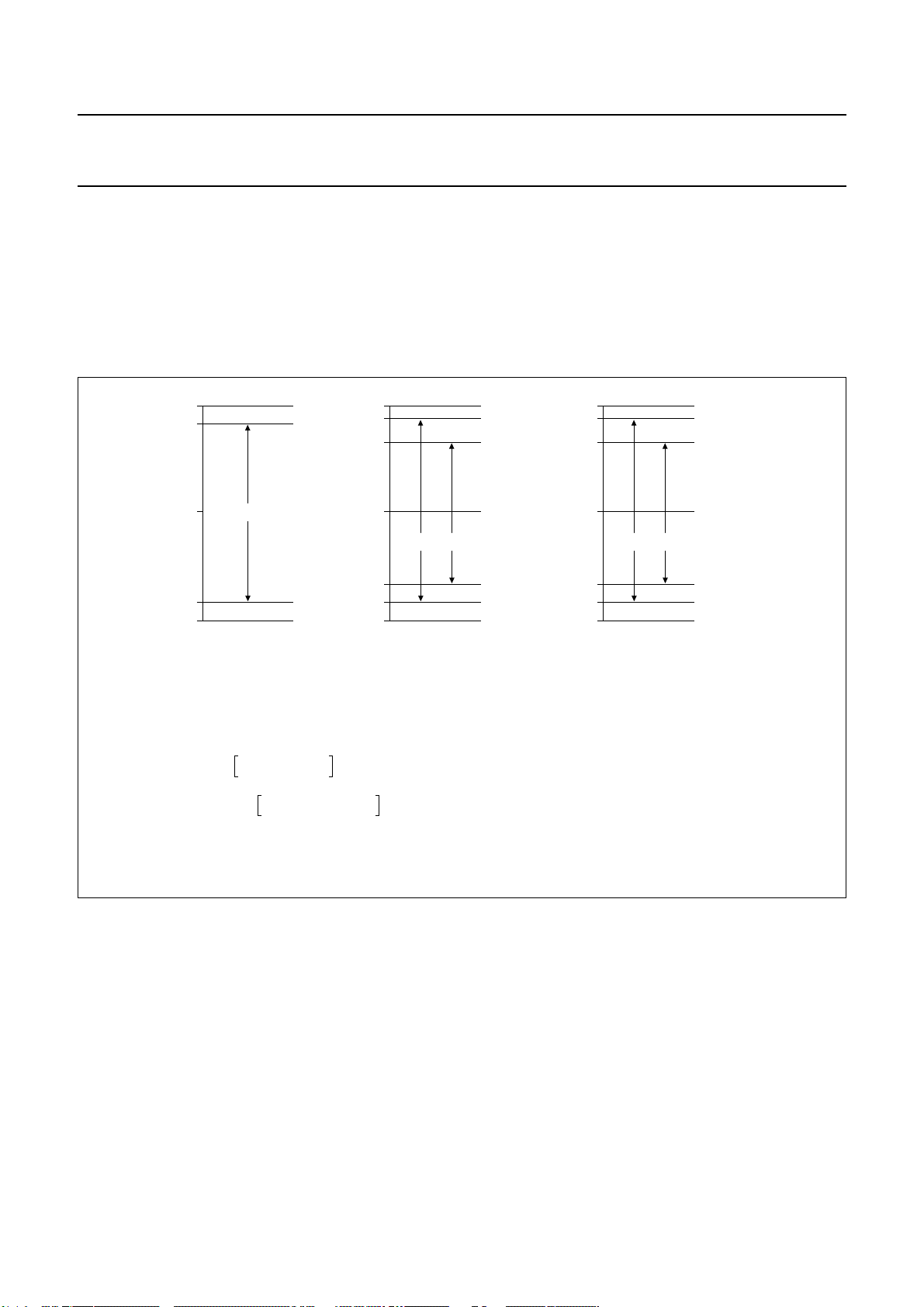
8.1.3.3 Brightness Contrast Saturation (BCS) control and decoder output levels
The resulting Y (CVBS) and CB-CR signals are fed to the BCS block, which contains the following functions:
• Chrominance saturation control by DSAT7 to DSAT0
• Luminance contrast and brightness control by DCON7 to DCON0 and DBRI7 to DBRI0
• Raw data (CVBS) gain and offset adjustment by RAWG7 to RAWG0 and RAWO7 to RAWO0
• Limiting Y-CB-CR or CVBS to the values 1 (minimum) and 254 (maximum) to fulfil
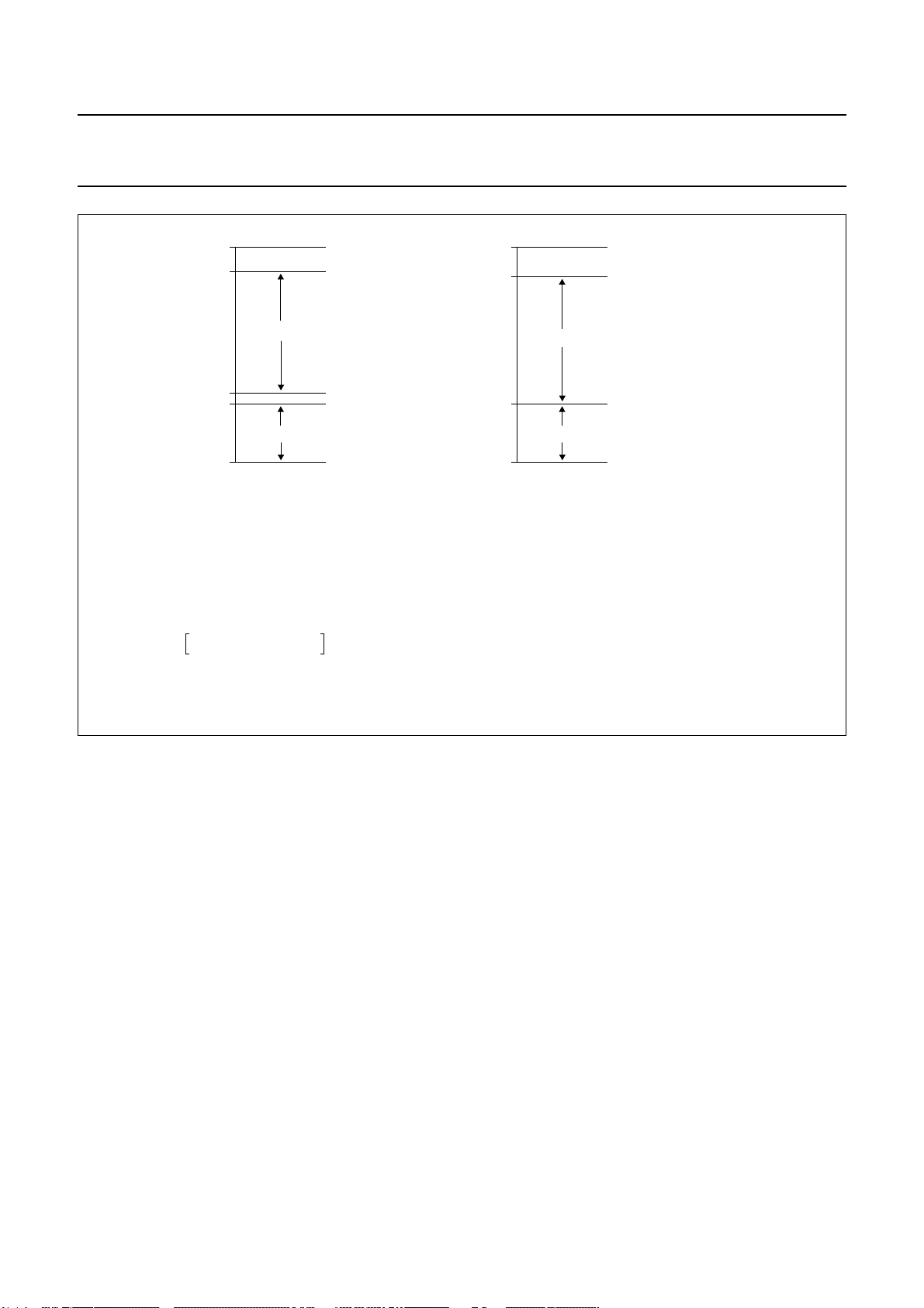
handbook, full pagewidth
+255
+235
+128
LUMINANCE 100%
+16
0
white
black
+255
+240
+212 +212
+128
CB-COMPONENT
+44
+16
0
blue 100%
blue 75%
colourless
yellow 75%
yellow 100%
+255
+240
+128
“ITU Recommendation 601/656”
red 100%
red 75%
colourless
CR-COMPONENT
+44
+16
0
cyan 75%
cyan 100%
MHB730
.
a. Y output range. b. CB output range. c. CR output range.
“ITU Recommendation 601/656”
Equations for modification to the Y-CB-CR levels via BCS control I2C-bus bytes DBRI, DCON and DSAT.
Luminance:
Chrominance:
It should be noted that the resulting levels are limited to 1 to 254 in accordance with
Y
OUT
CRCB()
OUT
digital levels with default BCS (decoder) settings DCON[7:0] = 44H, DBRI[7:0] = 80H and DSAT[7:0] = 40H.
DCON
Int
-----------------
Int
68
DSAT
--------------- 64
Y 128–()× DBRI+=
CRCB, 128–()× 128+=
“ITU Recommendation 601/656”
Fig.18 Y-CB-CR range for scaler input and X port output.
.
2004 Mar 03 32
Page 33
Philips Semiconductors Product specification
PAL/NTSC/SECAM video decoder with adaptive PAL/NTSC
comb filter, VBI data slicer and high performance scaler
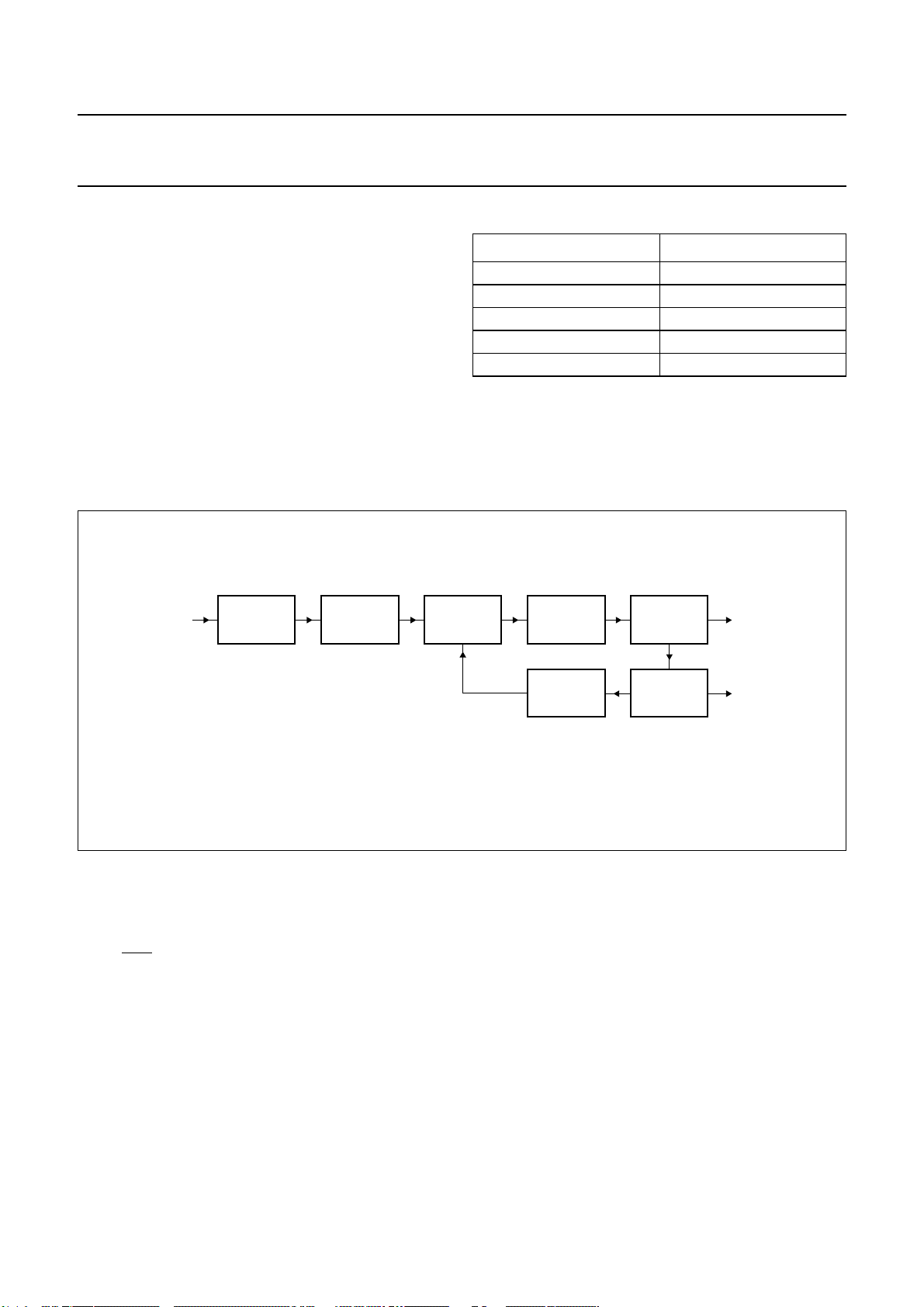
+255
+209
+71
+60
LUMINANCE
SYNC
1
white
black
black shoulder
sync bottom
a. Sources containing 7.5 IRE black level offset
(e.g. NTSC M).
+255
+199
LUMINANCE
+60
SYNC
1
white
black shoulder = black
sync bottom
b. Sources not containing black level offset.
SAA7114
MGD700
CVBS levels with default settings RAWG[7:0] = 64 and RAWO[7:0] = 128.
Equation for modification of the raw data levels via bytes RAWG and RAWO:
CVBS
OUT
It should be noted that the resulting levels are limited to 1 to 254 in accordance with “
Int
RAWG
-----------------64
CVBS
nom
128–()× RAWO+=
ITU Recommendation 601/656”
.
Fig.19 CVBS (raw data) range for scaler input, data slicer and X port output.
8.1.4 SYNCHRONIZATION
The prefiltered luminance signal is fed to the synchronization stage. Its bandwidth is further reduced to 1 MHz in a
low-pass filter. The sync pulses are sliced and fed to the phase detectors where they are compared with the sub-divided
clockfrequency.Theresultingoutputsignalisappliedtotheloopfiltertoaccumulateallphase deviations. Internal signals
(e.g. HCL and HSY) are generated in accordance with analog front-end requirements. The loop filter signal drives an
oscillator to generate the line frequency control signal LFCO; see Fig.20.
The detection of ‘pseudo syncs’ as part of the Macrovision copy protection standard is also achieved within the
synchronization circuit.
The result is reported as flag COPRO within the decoder status byte at subaddress 1FH.
2004 Mar 03 33
Page 34
Philips Semiconductors Product specification
PAL/NTSC/SECAM video decoder with adaptive PAL/NTSC
comb filter, VBI data slicer and high performance scaler
8.1.5 CLOCK GENERATION CIRCUIT
The internal CGC generates all clock signals required for
the video input processor.
The internal signal LFCO is a digital-to-analog converted
signal provided by the horizontal PLL. It is the multiple of
the line frequency:
6.75 MHz = 429 × fH (50 Hz), or
6.75 MHz = 432 × fH (60 Hz).
The LFCO signal is multiplied by a factor of 2 and 4 in the
internalPLL circuit (including phase detector, loop filtering,
VCO and frequency divider) to obtain the output clock
signals. The rectangular output clocks have a 50% duty
factor.
Table 3 Decoder clock frequencies
CLOCK FREQUENCY (MHz)
XTALO 24.576 or 32.110
LLC 27
LLC2 13.5
LLC4 (internal) 6.75
LLC8 (virtual) 3.375
SAA7114
LFCO
BAND PASS
FC = LLC/4
ZERO
CROSS
DETECTION
DETECTION
Fig.20 Block diagram of the clock generation circuit.
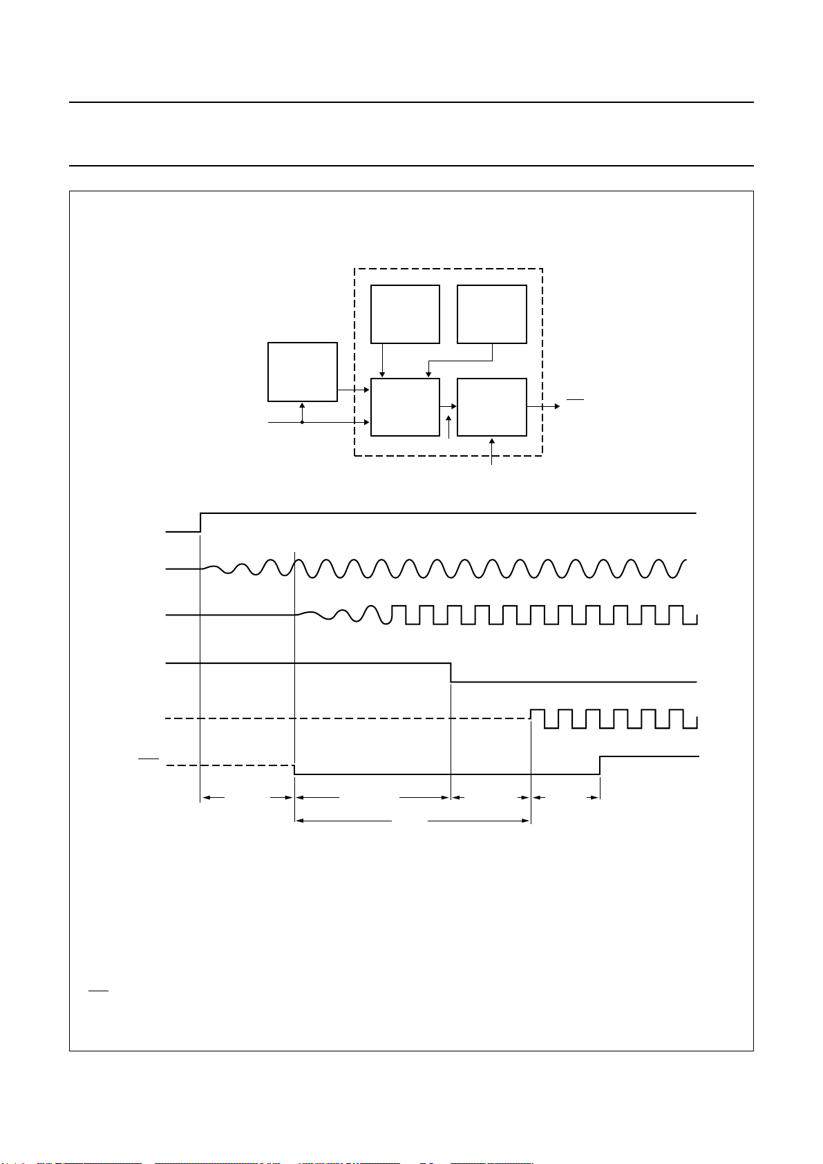
8.1.6 POWER-ON RESET AND CHIP ENABLE (CE) INPUT
A missing clock, insufficient digital or analog V
DDA0
supply
voltages (below 2.7 V) will start the reset sequence; all
outputs are forced to 3-state (see Fig.21). The indicator
output RES is LOW for approximately 128 LLC after the
internal reset and can be applied to reset other circuits of
the digital TV system.
PHASE
LOOP
FILTER
DIVIDER
1/2
OSCILLATOR
DIVIDER
1/2
MHB330
LLC
LLC2
It is possible to force a reset by pulling the Chip Enable pin
(CE) to ground. After the rising edge of CE and sufficient
power supply voltage, the outputs LLC, LLC2 and SDA
return from 3-state to active, while the other signals have
to be activated via programming.
2004 Mar 03 34
Page 35
Philips Semiconductors Product specification
PAL/NTSC/SECAM video decoder with adaptive PAL/NTSC
comb filter, VBI data slicer and high performance scaler
CE
CE
CLOCK
PLL
LLC
POC V
ANALOG
POC
LOGIC
DDA
RESINT
POC V
DIGITAL
POC
DELAY
CLK0
DDD
RES
SAA7114
XTALO
LLCINT
RESINT
LLC
RES
(internal
reset)
POC = Power-on control.
CE = chip enable input.
XTALO = crystal oscillator output.
LLCINT = internal system clock.
RESINT = internal reset.
LLC = line-locked clock output.
RES = reset output.
some ms
20 to 200 µs
PLL-delay
<
1 ms
896 LCC
digital delay
128 LCC
MHB331
Fig.21 Power-on control circuit.
2004 Mar 03 35
Page 36
Philips Semiconductors Product specification
PAL/NTSC/SECAM video decoder with adaptive PAL/NTSC
SAA7114
comb filter, VBI data slicer and high performance scaler
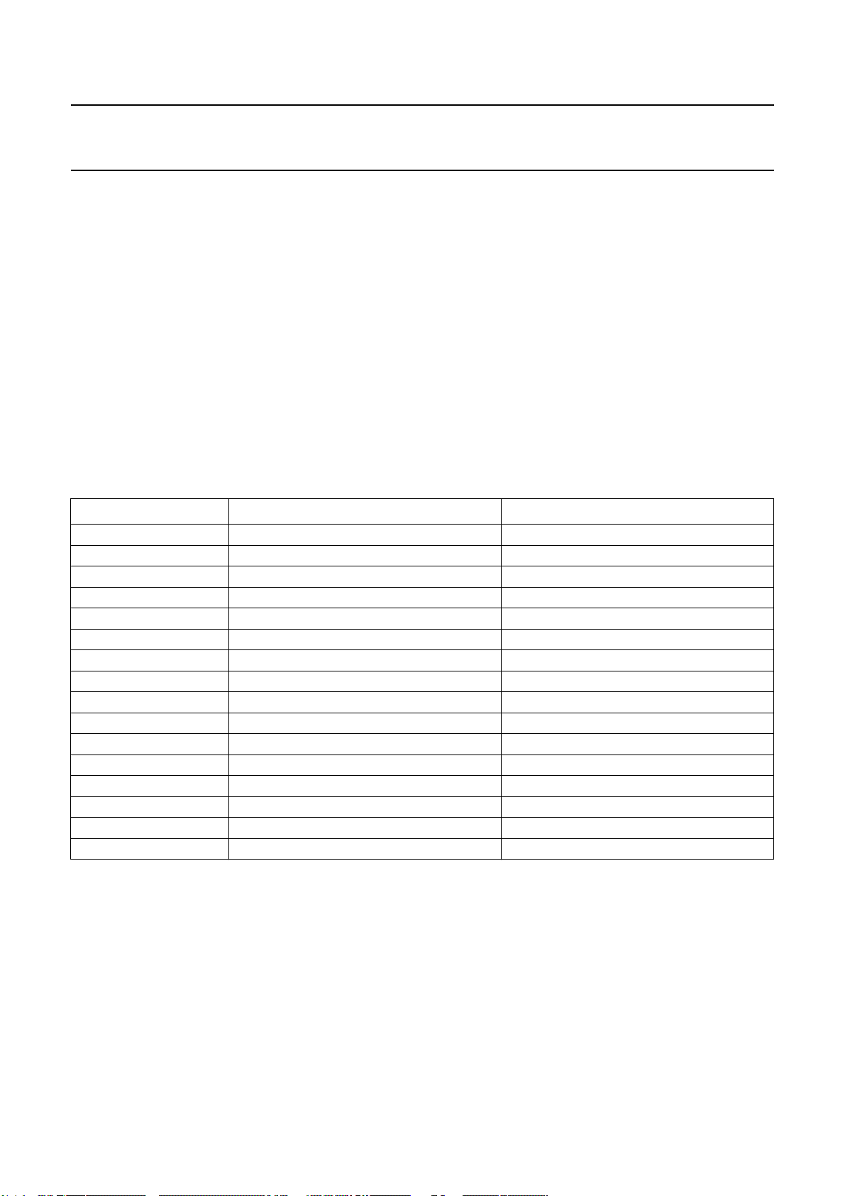
8.2 Decoder output formatter
The output interface block of the decoder part contains the
ITU 656formatter for the expansion port data output XPD7
to XPD0 (for a detailed description see Section 9.4.1) and
the control circuit for the signals needed for the internal
paths to the scaler and data slicer part. It also controls the
selection of the reference signals for the RT port (RTCO,
RTS0 and RTS1) and the expansion port (XRH, XRV
and XDQ).
The generation of the decoder data type control signals
SET_RAW and SET VBI is also done within this block.
These signals are decoded from the requested data type
for the scaler input and/or the data slicer, selectable by the
control registers LCR2 to LCR24 (see also Chapter 15;
subaddresses 41H to 57H).
Table 4 Data formats at decoder output
DATA TYPE NUMBER DATA TYPE DECODER OUTPUT DATA FORMAT
0 teletext EuroWST, CCST raw
1 European closed caption raw
2 Video Programming Service (VPS) raw
3 wide screen signalling bits raw
4 US teletext (WST) raw
5 US closed caption (line 21) raw
6 video component signal, VBI region Y-CB-CR 4:2:2
7 CVBS data raw
8 teletext raw
9 VITC/EBU time codes (Europe) raw
10 VITC/SMPTE time codes (USA) raw
11 reserved raw
12 US NABTS raw
13 MOJI (Japanese) raw
14 Japanese format switch (L20/22) raw
15 video component signal, active video region Y-CB-CR 4:2:2
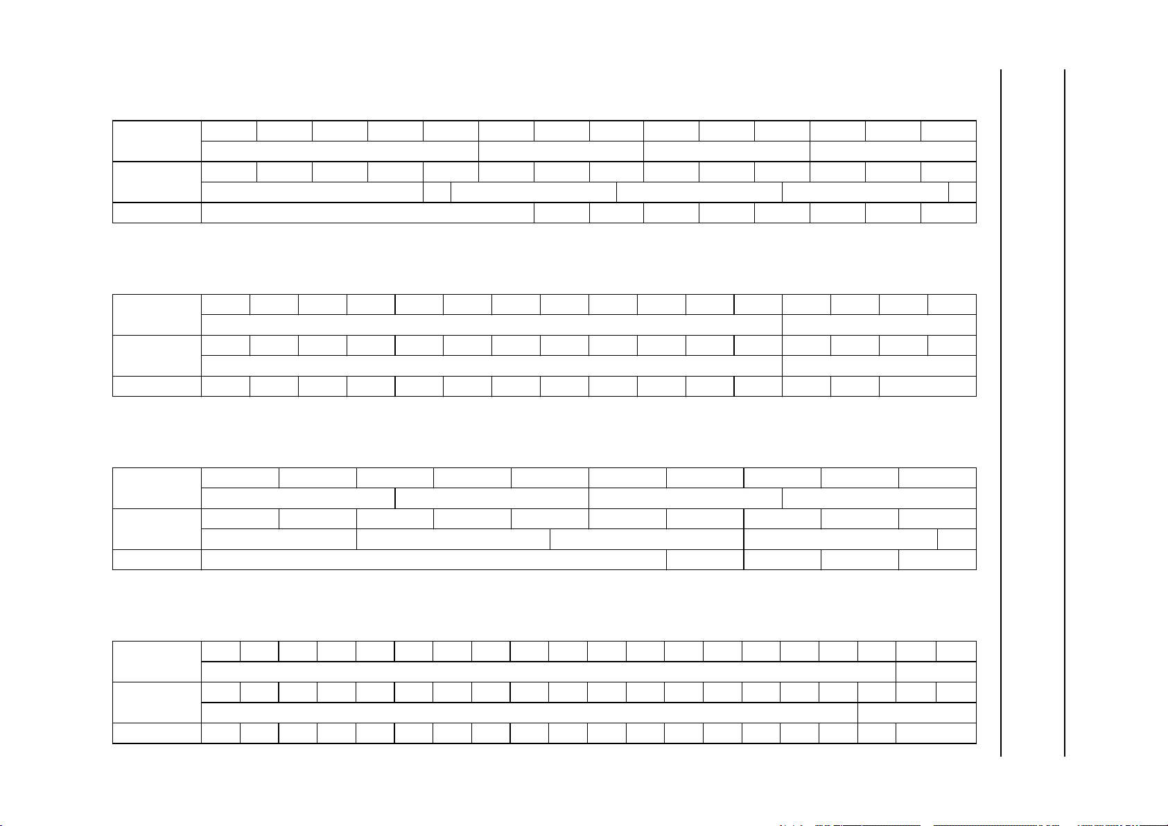
For each LCR value from 2 to 23 the data type can be
programmed individually; LCR2 to LCR23 refer to line
numbers. The selection in LCR24 values is valid for the
rest of the corresponding field. The upper nibble contains
the value for field 1 (odd), the lower nibble for field 2
(even). The relationship between LCR values and line
numbers can be adjusted via VOFF8 to VOFF0, locatedin
subaddresses 5BH (bit D4) and 5AH (bits D7 to D0) and
FOFF subaddress 5BH (bit D7). The recommended
values are VOFF[8:0] = 03H for 50 Hz sources (with
FOFF = 0) and VOFF[8:0] = 06H for 60 Hz sources (with
FOFF = 1), to accommodate line number conventions as
used for PAL, SECAM and NTSC standards;
see Tables 5 to 8.
2004 Mar 03 36
Page 37
This text is here in white to force landscape pages to be rotated correctly when browsing through the pdf in the Acrobat reader.This text is here in
_white to force landscape pages to be rotated correctly when browsing through the pdf in the Acrobat reader.This text is here inThis text is here in
white to force landscape pages to be rotated correctly when browsing through the pdf in the Acrobat reader. white to force landscape pages to be ...
2004 Mar 03 37
Table 5 Relationship of LCR to line numbers in 525 lines/60 Hz systems (part 1)
Vertical line offset, VOFF[8:0] = 06H (subaddresses 5BH[4] and 5AH[7:0]); horizontal pixel offset, HOFF[10:0] = 347H (subaddresses 5BH[2:0] and
59H[7:0]); FOFF = 1 (subaddress 5BH[7])
Linenumber
(1st field)
Linenumber
(2nd field)
LCR 24 23456789
Table 6 Relationship of LCR to line numbers in 525 lines/60 Hz systems (part 2)
Vertical line offset, VOFF[8:0] = 06H (subaddresses 5BH[4] and 5AH[7:0]); horizontal pixel offset, HOFF[10:0] = 347H (subaddresses 5BH[2:0] and
59H[7:0]); FOFF = 1 (subaddress 5BH[7])
Linenumber
(1st field)
Linenumber
(2nd field)
LCR 10 11 12 13 14 15 16 17 18 19 20 21 22 23 24
521 522 523 524 525 1 2 3 4 5 6 7 8 9
active video equalization pulses serration pulses equalization pulses
259 260 261 262 263 264 265 266 267 268 269 270 271 272
active video equalization pulses serration pulses equalization pulses
10 11 12 13 14 15 16 17 18 19 20 21 22 23 24 25
nominal VBI lines F1 active video
273 274 275 276 277 278 279 280 281 282 283 284 285 286 287 288
nominal VBI lines F2 active video
Philips Semiconductors Product specification
PAL/NTSC/SECAM video decoder with adaptive PAL/NTSC
comb filter, VBI data slicer and high performance scaler
Table 7 Relationship of LCR to line numbers in 625 lines/50 Hz systems (part 1)
Vertical line offset, VOFF[8:0] = 03H (subaddresses 5BH[4] and 5AH[7:0]); horizontal pixel offset, HOFF[10:0] = 347H (subaddresses 5BH[2:0] and
59H[7:0]); FOFF = 0 (subaddress 5BH[7])
Linenumber
(1st field)
Linenumber
(2nd field)
LCR 24 2345
Table 8 Relationship of LCR to line numbers in 625 lines/50 Hz systems (part 2)
Vertical line offset, VOFF[8:0] = 03H (subaddresses 5BH[4] and 5AH[7:0]); horizontal pixel offset, HOFF[10:0] = 347H (subaddresses 5BH[2:0] and
59H[7:0]); FOFF = 0 (subaddress 5BH[7])
Linenumber
(1st field)
Linenumber
(2nd field)
LCR 6 7 8 9 10 11 12 13 14 15 16 17 18 19 20 21 22 23 24
62162262362462512345
active video equalization pulses serration pulses equalization pulses
309 310 311 312 313 314 315 316 317 318
active video equalization pulses serration pulses equalization pulses
6 7 8 9 10 11 12 13 14 15 16 17 18 19 20 21 22 23 24 25
nominal VBI lines F1 active video
319 320 321 322 323 324 325 326 327 328 329 330 331 332 333 334 335 336 337 338
nominal VBI lines F2 active video
SAA7114
Page 38
Philips Semiconductors Product specification
PAL/NTSC/SECAM video decoder with adaptive PAL/NTSC
comb filter, VBI data slicer and high performance scaler
625
1
2
3
4
5
6
ITU counting
single field counting
CVBS
HREF
F_ITU656
(1)
V123
VGATE
FID
ITU counting
single field counting
CVBS
623
622
310
309
VSTO[8:0] = 134H
310
309
310
309
624
311
311
311
312
312
312
1
2
3
4
5
(a) 1st field
313
31413152316331743185319
313
7
6
7
6
22
...
22
...
VSTA[8:0] = 15H
335
...
22
...
SAA7114
23
23
336
23
HREF
F_ITU656
(1)
V123
VGATE
FID
VSTO[8:0] = 134H
(b) 2nd field
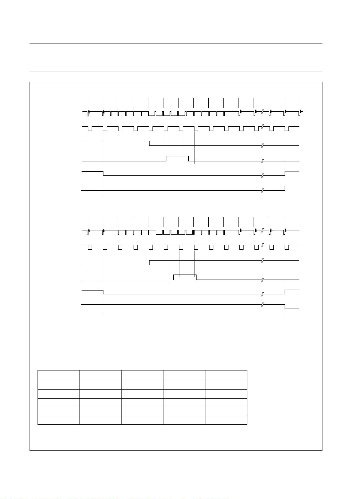
(1) The inactive going edge of the V123 signal indicates whether the field is odd or even. If HREF is active during
the falling edge of V123, the field is ODD (field 1). If HREF is inactive during the falling edge of V123, the field
is EVEN. The specific position of the slope is dependent on the internal processing delay and may change a
few clock cycles from version to version.
The control signals listed above are available on pins RTS0, RTS1, XRH and XRV according to the following table:
NAME RTS0 RTS1 XRH XRV
HREF X X X −
F_ITU656 −−−X
V123 X X − X
VGATE X X −−
FID X X −−
For further information see Section 15.2: Tables 57, 58 and 59.
VSTA[8:0] = 15H
MHB540
Fig.22 Vertical timing diagram for 50 Hz/625 line systems.
2004 Mar 03 38
Page 39
Philips Semiconductors Product specification
PAL/NTSC/SECAM video decoder with adaptive PAL/NTSC
comb filter, VBI data slicer and high performance scaler
3
4
5
6
7
8
ITU counting
single field counting
CVBS
HREF
F_ITU656
(1)
V123
VGATE
FID
ITU counting
single field counting
CVBS
525
262
VSTO[8:0] = 101H
263
262
263
262
2
1
1
3
4
5
6
2
7
(a) 1st field
265
264
1
266326742685269627072718272
2
9910
8
10
9
21
...
21
...
VSTA[8:0] = 011H
284
...
21
...
SAA7114
22
22
285
22
HREF
F_ITU656
(1)
V123
VGATE
FID
VSTO[8:0] = 101H
(b) 2nd field
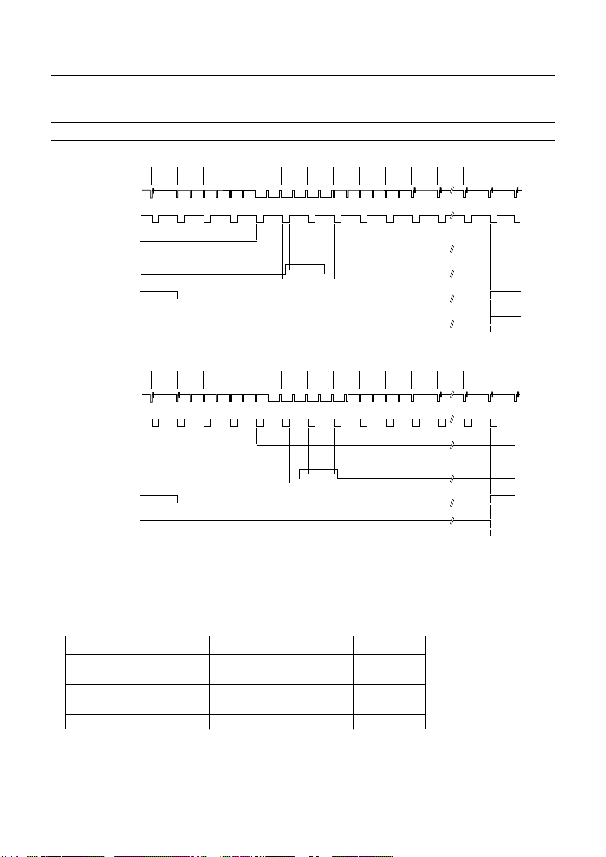
(1) The inactive going edge of the V123 signal indicates whether the field is odd or even. If HREF is active during
the falling edge of V123, the field is ODD (field 1). If HREF is inactive during the falling edge of V123, the field
is EVEN. The specific position of the slope is dependent on the internal processing delay and may change a
few clock cycles from version to version.
The control signals listed above are available on pins RTS0, RTS1, XRH and XRV according to the following table:
NAME RTS0 RTS1 XRH XRV
HREF X X X −
F_ITU656 −−−X
V123 X X − X
VGATE X X −−
FID X X −−
For further information see Section 15.2: Tables 57, 58 and 59.
VSTA[8:0] = 011H
MHB541
Fig.23 Vertical timing diagram for 60 Hz/525 line systems.
2004 Mar 03 39
Page 40
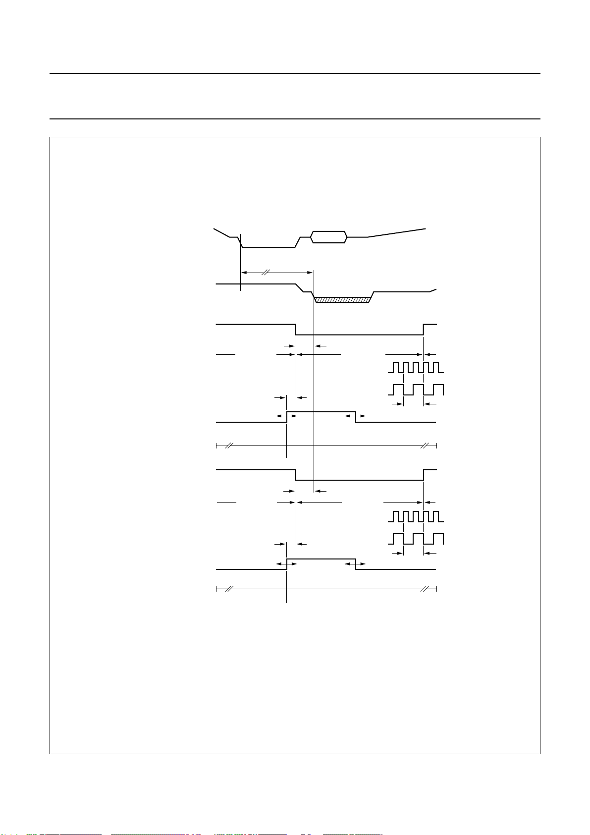
Philips Semiconductors Product specification
PAL/NTSC/SECAM video decoder with adaptive PAL/NTSC
comb filter, VBI data slicer and high performance scaler
CVBS input
expansion port
data output
HREF (50 Hz)
CREF
processing delay ADC to expansion port:
140 × 1/LLC
720 × 2/LLC
burst
sync clipped
12 × 2/LLC
144 × 2/LLC
SAA7114
CREF2
HS (50 Hz)
programming range
(step size: 8/LLC)
HREF (60 Hz)
CREF
CREF2
HS (60 Hz)
programming range
(step size: 8/LLC)
108
107
5 × 2/LLC
720 × 2/LLC
1 × 2/LLC
2 × 2/LLC
0
16 × 2/LLC
138 × 2/LLC
2 × 2/LLC
0
−107
−106
MHB542
The signals HREF, HS, CREF2 and CREF are available on pins RTS0 and/or RTS1 (see Section 15.2.19 Tables 57 and 58);
their polarity can be inverted via RTP0 and/or RTP1.
The signals HREF and HS are available on pin XRH (see Section 15.2.20 Table 59).
Fig.24 Horizontal timing diagram (50/60 Hz).
2004 Mar 03 40
Page 41

Philips Semiconductors Product specification
PAL/NTSC/SECAM video decoder with adaptive PAL/NTSC
comb filter, VBI data slicer and high performance scaler
8.3 Scaler
TheHigh Performance video Scaler (HPS) is basedon the
system as implemented in previous products (e.g.
SAA7140), but with some aspects enhanced. Vertical
upsampling is supported and the processing pipeline
buffer capacity is enhanced, to allow more flexible video
stream timing at the image port, discontinuous transfers,
and handshake. The internal data flow from block to block
is discontinuous dynamically, due to the scaling process.
The flow is controlled by internal data valid and data
request flags (internal handshake signalling) between the
sub-blocks; therefore the entire scaler acts as a pipeline
buffer. Depending on the actually programmed scaling
parameters the effective buffer can exceed to an entire
line. The access/bandwidth requirements to the VGA
frame buffer are reduced significantly.
The high performance video scaler in the SAA7114 has
the following major blocks:
• Acquisition control (horizontal and vertical timer) and
task handling (the region/field/frame based processing)
• Prescaler, for horizontal downscaling by an integer
factor, combined with appropriate band limiting filters,
especially anti-aliasing for CIF format
• Brightness,saturation,contrast control for scaled output
data
• Line buffer, with asynchronous read and write, to
support vertical upscaling (e.g. for videophone
application, converting 240 into 288 lines, Y-CB-C
4:2:2)
• Vertical scaling, with phase accurate Linear Phase
Interpolation (LPI) for zoom and downscale, or phase
accurate Accumulation Mode (ACM) for large
downscaling ratios and better alias suppression
• Variable Phase Delay (VPD), operates as horizontal
phase accurate interpolation for arbitrary non-integer
scaling ratios, supporting conversion between square
and rectangular pixel sampling
• Output formatter for scaled Y-CB-CR4:2:2,
Y-CB-CR4:1:1 and Yonly (format also used for raw
data)
• FIFO, 32-bit wide, with 64 pixel capacity in Y-CB-C
formats
• Output interface, 8 or 16-bit (only if extended by H port)
data pins wide, synchronous or asynchronous
operation, with stream events on discrete pins, or coded
in the data stream.
R
R
The overall H and V zooming (HV_zoom) is restricted by
the input/output data rate relationships. With a safety
margin of 2% for running in and running out, the maximum
HV_zoom is equal to:
×
0.98
-------------------------------------------------------------------------------------------------------------------------------------in_pixel in_lines× out_cycle_per_pix× T_out_clk×
For example:
1. Input from decoder: 50 Hz, 720 pixel, 288 lines, 16-bit
data at 13.5 MHz data rate, 1 cycle per pixel; output:
8-bit data at 27 MHz, 2 cycles per pixel; the maximum
HV_zoom is equal to:
0.98
2. Input from X port: 60 Hz, 720 pixel, 240 lines, 8-bit
data at 27 MHz data rate (ITU 656), 2 cycles per pixel;
output via I + H port: 16-bit data at 27 MHz clock,
1 cycle per pixel; the maximum HV_zoom is equal to:
0.98
The video scaler receives its input signal from the video
decoder or from the expansion port (X port). It gets 16-bit
Y-CB-CR 4:2:2 input data at a continuous rate of
13.5 MHz from the decoder. Discontinuous data stream
can be accepted from the expansion port (X port),
normally 8-bit wide ITU 656 such as Y-CB-CR data,
accompanied by a pixel qualifier on XDQ.
Theinputdatastreamis sorted into two data paths, one for
luminance (or raw samples) and one for time multiplexed
chrominance CBand CR samples. An Y-CB-CR 4:1:1
input format is converted to 4 :2:2 for the horizontal
prescaling and vertical filter scaling operation.
Thescaler operation is defined by twoprogrammingpages
A and B, representing two different tasks, that can be
applied field alternating or to define two regions in a field
(e.g.with different scaling range, factors and signal source
during odd and even fields).
Each programming page contains control:
• For signal source selection and formats
• For task handling and trigger conditions
• For input and output acquisition window definition
• For H-prescaler, V-scaler and H-phase scaling.
Raw VBI data is handled as a specific input format and
needs its own programming page (equals own task).
T_input_field T_v_blanking–
20 ms 24 64 µs×–
-------------------------------------------------------720 288× 2× 37 ns×
16.666 ms 22 64 µs×–
-------------------------------------------------------------720 240× 1× 37 ns×
SAA7114
1.18=×
2.34=×
2004 Mar 03 41
Page 42

Philips Semiconductors Product specification
PAL/NTSC/SECAM video decoder with adaptive PAL/NTSC
comb filter, VBI data slicer and high performance scaler
In VBI pass through operation the processing of prescaler
and vertical scaling has to be set to no-processing,
however, the horizontal fine scaling VPD can be activated.
Upscaling (oversampling, zooming), free of frequency
folding, up to a factor of 3.5 can be achieved, as required
by some software data slicing algorithms.
These raw samples are transported through the image
port as valid data and can be output as Y only format. The
lines are framed by SAV and EAV codes.
8.3.1 ACQUISITION CONTROL AND TASK HANDLING
(SUBADDRESSES 80H, 90H, 91H, 94H TO 9FH
AND C4H TO CFH)
The acquisition control receives horizontal and vertical
synchronization signals from the decoder section or from
the X port. The acquisition window is generated via pixel
and line counters at the appropriate places in the data
path. From X port only qualified pixels and lines (lines with
qualified pixel) are counted.
8.3.1.1 Input field processing
The trigger event for the field sequence detection from
external signals (X port) are defined in subaddress 92H.
From the X port the state of the scalers H reference signal
at the time of the V reference edge is taken as field
sequence identifier FID. For example, if the falling edge of
the XRV input signal is the reference and the state of XRH
input is logic 0 at that time, the detected field ID is logic 0.
The bits XFDV[92H[7]] and XFDH[92H[6]] define the
detection event and state of the flag from the X port. For
the default setting of XFDV and XFDH at ‘00’ the state of
the H-input at the falling edge of the V-input is taken.
The scaler directly gets a corresponding field ID
information from the SAA7114 decoder path.
The FID flag is used to determine whether the first or
second field of a frame is going to be processed within the
scaler and it is used as trigger condition for the task
handling (see bits STRC[1:0] 90H[1:0]).
SAA7114
The acquisition window parameters are as follows:
• Signal source selection regarding input video stream
and formats from the decoder, or from X port
(programming bits SCSRC[1:0] 91H[5:4] and FSC[2:0]
91H[2:0])
Remark: The input of raw VBI data from the internal
decoder should be controlled via the decoder output
formatter and the LCR registers; see Section 8.2
• Vertical offset defined in lines of the video source,
parameter YO[11:0] 99H[3:0] 98H[7:0]
• Vertical length defined in lines of the video source,
parameter YS[11:0] 9BH[3:0] 9AH[7:0]
• Vertical length defined in number of target lines, as a
result of vertical scaling, parameter YD[11:0] 9FH[3:0]
9EH[7:0]
• Horizontaloffset defined in number of pixels ofthe video
source, parameter XO[11:0] 95H[3:0] 94H[7:0]
• Horizontal length defined in number of pixels of the
video source, parameter XS[11:0] 97H[3:0] 96H[7:0]
• Horizontal destination size, defined in target pixels after
fine scaling, parameter XD[11:0] 9DH[3:0] 9CH[7:0].
The source start offset (XO11 to XO0 and YO11 to YO0)
opens the acquisition window, and the target size
(XD11 to XD0 and YD11 to YD0) closes the window,
howeverthe window is cut vertically if there are less output
lines than expected. The trigger events for the pixel and
line counts are the horizontal and vertical reference edges
as defined in subaddress 92H. The task handling is
controlled by subaddress 90H; see Section 8.3.1.2.
According to ITU 656, when FID is at logic 0 means first
field of a frame. To ease the application, the polarities of
the detection results on the X port signals and the internal
decoder ID can be changed via XFDH.
As the V-sync from the decoder path has a half line timing
(due to the interlaced video signal), but the scaler
processing only knows about full lines, during 1st fields
fromthe decoder the line count of the scaler possibly shifts
by one line, compared to the 2nd field. This can be
compensated for by switching the V-trigger event, as
defined by XDV0, to the opposite V-sync edge or by using
theverticalscalers phase offsets. The vertical timing of the
decoder can be seen in Figs 22 and 23.
As the H and V reference events inside the ITU 656 data
stream (from X port) and the real-time reference signals
from the decoder path are processed differently, the
trigger events for the input acquisition also have to be
programmed differently.
2004 Mar 03 42
Page 43
Philips Semiconductors Product specification
PAL/NTSC/SECAM video decoder with adaptive PAL/NTSC
SAA7114
comb filter, VBI data slicer and high performance scaler
Table 9 Processing trigger and start
XDV1
92H[5]
0 1 0 4/7 (50/60 Hz, 1st field), respectively 3/6 (50/60 Hz, 2nd field) (decoder count)
0 0 0 2/5 (50/60 Hz, 1st field), respectively 2/5 (50/60 Hz, 2nd field) (decoder count)
000External ITU 656 stream: The processing starts earliest with SAV at line number 23
8.3.1.2 Task handling
The task handler controls the switching between the two
programming register sets. It is controlled by
subaddresses 90H and C0H. A task is enabled via the
global control bits TEA[80H[4]] and TEB[80H[5]].
The handler is then triggered by events, which can be
defined for each register set.
In the event of a programming error the task handling and
the complete scaler can be reset to the initial states by
setting the software reset bit SWRST[88H[5]] to logic 0.
Especiallyif the programming registers, relatedacquisition
windowand scale are reprogrammed whileatask is active,
a software reset must be performed after programming.
Contrary to the disabling/enabling of a task, which is
evaluated at the end of a running task, when SWRST is at
logic 0 it sets the internal state machines directly to their
idle states.
The start condition for the handler is defined by bits
STRC[1:0]90H[1:0]andmeans:startimmediately,waitfor
next V-sync, next FID at logic 0 or next FID at logic 1. The
FID is evaluated, if the vertical and horizontal offsets are
reached.
When RPTSK[90H[2]] is at logic 1 the actual running task
is repeated (under the defined trigger conditions), before
handing control over to the alternate task.
To support field rate reduction, the handler is also enabled
to skip fields (bits FSKP[2:0] 90H[5:3]) before executing
thetask.ATOGGLEflagisgenerated(usedfor the correct
output field processing), which changes state at the
beginning of a task, every time a task is activated;
examples are given in Section 8.3.1.3.
XDV0
92H[4]
XDH
92H[2]
DESCRIPTION
Internal decoder: The processing triggers at the falling edge of the V123 pulse
[see Figs 22 (50 Hz) and 23 (60 Hz)], and starts earliest with the rising edge of the
decoder HREF at line number:
(50 Hz system), respectively line 20 (60 Hz system) (according to ITU 656 count)
Remarks:
• To activate a task the start condition must be
fulfilled and the acquisition window offsets must be
reached.
For example, in case of ‘start immediately’, and two
regions are defined for one field, the offset of the lower
region must be greater than (offset + length) of the
upper region, if not, the actual counted H and V position
at the end of the upper task is beyond the programmed
offsets and the processing will ‘wait for next V’.
• Basicallythe trigger conditions are checked, when a
task is activated. It is important to realize, that they are
not checked while a task is inactive. So you can not
trigger to next logic 0 or logic 1 with overlapping offset
and active video ranges between the tasks (e.g. task A
STRC[2:0] = 2, YO[11:0] = 310 and task B
STRC[2:0] = 3, YO[11:0] = 310 results in output field
rate of50⁄3Hz).
• After power-on or software reset (via
SWRST[88H[5]]) task B gets priority over task A.
8.3.1.3 Output field processing
As a reference for the output field processing, two signals
are available for the back-end hardware.
These signals are the input field ID from the scaler source
and a TOGGLE flag, which shows that an active task is
used an odd (1, 3, 5...) or even (2, 4, 6...) number of times.
Usingasingleorboth tasks and reducing the field or frame
rate with the task handling function, the TOGGLE
information can be used to reconstruct an interlaced
scaled picture at a reduced frame rate. The TOGGLE flag
isn’t synchronized to the input field detection, as it is only
dependent on the interpretation of this information by the
external hardware, whether the output of the scaler is
processed correctly; see Section 8.3.3.
2004 Mar 03 43
Page 44
This text is here in white to force landscape pages to be rotated correctly when browsing through the pdf in the Acrobat reader.This text is here in
_white to force landscape pages to be rotated correctly when browsing through the pdf in the Acrobat reader.This text is here inThis text is here in
white to force landscape pages to be rotated correctly when browsing through the pdf in the Acrobat reader. white to force landscape pages to be ...
2004 Mar 03 44
With OFIDC = 0, the scalers input field ID is available as output field ID on bit D6 of SAV and EAV, respectively on pin IGP0 (IGP1), if FID output is
selected.
When OFIDC[90H[6]] = 1, the TOGGLE information is available as output field ID on bit D6 of SAV and EAV, respectively on pin IGP0 (IGP1), if FID
output is selected.
Additionally the bit D7 of SAV and EAV can be defined via CONLH[90H[7]]. CONLH[90H[7]] = 0 (default) sets D7 to logic 1, a logic 1 inverts the
SAV/EAV bit D7. So it is possible to mark the output of the both tasks by different SAV/EAV codes. This bit can also be seen as ‘task flag’ on the
pins IGP0 (IGP1), if TASK output is selected.
Table 10 Examples for field processing
FIELD SEQUENCE FRAME/FIELD
SUBJECT
EXAMPLE 1
(1)
EXAMPLE 2
(2)(3)
EXAMPLE 3
(2)(4)(5)
EXAMPLE 4
(2)(4)(6)
1/1 1/2 2/1 1/1 1/2 2/1 2/2 1/1 1/2 2/1 2/2 3/1 3/2 1/1 1/2 2/1 2/2 3/1 3/2
Processed by task A A A B A B A B B A B B A B B A B B A
State of detected
01 00101010101 0 101 01
ITU 656 FID
TOGGLE flag 1 0 1 1 1 0 0 1 0 1 1 0 0 0
Bit D6 of SAV/EAV byte 0 1 0 0 1 0 1 1 0 1 1 0 0 0
Required sequence
conversion at the vertical
(8)
scaler
(9)
Output
UP
LO
UP
UP
LO
UP
LO
UP
LO
UP
LO
UP
LO
↓
↓
↓
↓
↓
↓
↓
↓
↓
↓
↓
↓
↓
UP
LO
UP
UP
LO
UP
LO
LO
UP
LO
LO
UP
UP
OO OOOOOOOOOOONOOONOOO
(7)
(7)
UP
↓
UP
111
111
LO
UP
↓
LO
LO
(7)
(7)
LO
↓
↓
LO
00
00
UP
LO
↓
↓
UP
UP
Philips Semiconductors Product specification
PAL/NTSC/SECAM video decoder with adaptive PAL/NTSC
comb filter, VBI data slicer and high performance scaler
Notes
1. Single task every field; OFIDC = 0; subaddress 90H at 40H; TEB[80H[5]] = 0.
2. Tasks are used to scale to different output windows, priority on task B after SWRST.
3. Both tasks at1⁄2frame rate; OFIDC = 0; subaddresses 90H at 43H and C0H at 42H.
4. In examples 3 and 4 the association between input FID and tasks can be flipped, dependent on which time the SWRST is de-asserted.
5. Task B at2⁄3frame rate constructed from neighbouring motion phases; task A at1⁄3frame rate of equidistant motion phases; OFIDC = 1;
subaddresses 90H at 41H and C0H at 45H.
6. Task A and B at1⁄3frame rate of equidistant motion phases; OFIDC = 1; subaddresses 90H at 41H and C0H at 49H.
7. State of prior field.
8. It is assumed that input/output FID = 0 (= upper lines); UP = upper lines; LO = lower lines.
9. O = data output; NO = no output.
SAA7114
Page 45

Philips Semiconductors Product specification
PAL/NTSC/SECAM video decoder with adaptive PAL/NTSC
comb filter, VBI data slicer and high performance scaler
8.3.2 HORIZONTAL SCALING
Theoverall horizontal required scaling factorhasto be split
into a binary and a rational value according to the
equation:
H-scale ratio
H-scale ratio
output pixel
=
-----------------------------input pixel
1
--------------------------- -
XPSC[5:0]
1024
×=
------------------------------XSCY[12:0]
wherethe parameter of prescaler XPSC[5:0] = 1 to 63 and
the parameter of VPD phase interpolation
XSCY[12:0] = 300 to 8191 (0 to 299 are only theoretical
values). For example,1⁄
is to split in1⁄4× 1.14286. The
3.5
binary factor is processed by the prescaler, the arbitrary
non-integer ratio is achieved via the variable phase delay
VPD circuitry, called horizontal fine scaling. The latter
calculates horizontally interpolated new samples with a
6-bit phase accuracy, which relates to less than 1 ns jitter
for regular sampling scheme. Prescaler and fine scaler
create the horizontal scaler of the SAA7114.
Using the accumulation length function of the prescaler
(XACL[5:0] A1H[5:0]), application and destination
dependent (e.g. scale for display or for a compression
machine), a compromise between visible bandwidth and
alias suppression can be determined.
• The bit XC2_1[A2H[3]], which defines the weighting of
the incoming pixels during the averaging process:
– XC2_1 = 0 ⇒ 1 + 1...+ 1 +1
– XC2_1 = 1 ⇒ 1 + 2...+ 2 +1.
Theprescaler creates a prescaledependentFIR low-pass,
with up to (64 + 7) filter taps. The parameter XACL[5:0]
can be used to vary the low-pass characteristic for a given
integer prescale of1⁄
XPSC[5:0]
decide between signal bandwidth (sharpness impression)
and alias.
Equation for XPSC[5:0] calculation is:
XPSC[5:0] lower integer of
=
Where:
the range is 1 to 63 (value 0 is not allowed);
Npix_in = number of input pixel, and
Npix_out = number of desired output pixel over the
complete horizontal scaler.
The use of the prescaler results in a XACL[5:0] and
XC2_1 dependent gain amplification. The amplification
can be calculated according to the equation:
DC gain = (XC2_1 + 1) × XACL[5:0] + (1 − XC2_1)
SAA7114
. The user can therefore
Npix_in
----------------------Npix_out
8.3.2.1 Horizontal prescaler (subaddresses
A0H to A7H and D0H to D7H)
The prescaling function consists of an FIR anti-alias filter
stage and an integer prescaler, which creates an adaptive
prescale dependent low-pass filter to balance sharpness
and aliasing effects.
The FIR prefilter stage implements different low-pass
characteristics to reduce alias for downscales in the range
of 1 to1⁄2. A CIF optimized filter is built-in, which reduces
artefacts for CIF output formats (to be used in combination
with the prescaler set to1⁄2scale); see Table 11.
The function of the prescaler is defined by:
• An integer prescaling ratio XPSC[5:0] A0H[5:0] (equals
1 to 63), which covers the integer downscale
range 1 to1⁄
63
• An averaging sequence length XACL[5:0] A1H[5:0]
(equals 0 to 63); range 1 to 64
• A DC gain renormalization XDCG[2:0] A2H[2:0];
1 down to1⁄
128
It is recommended to use sequence lengths and weights,
N
which results in a 2
DC gain amplification, as these
amplitudes can be renormalized by the XDCG[2:0]
controlled shifter of the prescaler.
The renormalization range of XDCG[2:0] is 1,
to1⁄
128
1
------
N
2
1
⁄2 down
.
Other amplifications have to be normalized by using the
following BCS control circuitry. In these cases the
prescaler has to be set to an overall gain of ≤1, e.g. for an
accumulation sequence of ‘1 + 1 + 1’ (XACL[5:0] = 2 and
XC2_1 = 0),XDCG[2:0] must be setto‘010’, this equals1⁄
and the BCS has to amplify the signal to4⁄3 (SATN[7:0]
and CONT[7:0] value = lower integer of4⁄3× 64).
The use of XACL[5:0] is XPSC[5:0] dependent.
XACL[5:0] must be <2 × XPSC[5:0].
XACL[5:0] can be used to find a compromise between
bandwidth (sharpness) and alias effects.
4
2004 Mar 03 45
Page 46
Philips Semiconductors Product specification
PAL/NTSC/SECAM video decoder with adaptive PAL/NTSC
comb filter, VBI data slicer and high performance scaler
Remark: Due to bandwidth considerations XPSC[5:0] and
XACL[5:0] can be chosen differently to the previously
mentioned equations or Table 12, as the H-phase scaling
is able to scale in the range from zooming up by factor 3 to
downscaling by a factor of
Figures 27 and 28 show some resulting frequency
characteristics of the prescaler.
Table 12 shows the recommended prescaler
programming. Other programmings, other than given in
Table 12, may result in better alias suppression, but the
resulting DC gain amplification needs to be compensated
by the BCS control, according to the equation:
CONT[7:0] SATN[7:0] lower integer of
Where:
XDCG[2:0]
2
DC gain = (XC2_1 + 1) × XACL[5:0] + (1 − XC2_1).
==
≥ DC gain
1024
⁄
8191
.
XDCG[2:0]
2
---------------------------------DC gain 64×
For example, if XACL[5:0] = 5, XC2_1 = 1, then the
DC gain = 10 and the required XDCG[2:0] = 4.
The horizontal source acquisition timing and the
prescalingratio is identical for both the luminance path and
chrominance path, but the FIR filter settings can be
defined differently in the two channels.
Fade-in and fade-out of the filters is achieved by copying
an original source sample each as first and last pixel after
prescaling.
Figures 25 and 26 show the frequency characteristics of
the selectable FIR filters.
SAA7114
Table 11 FIR prefilter functions
PFUV[1:0] A2H[7:6]
PFY[1:0] A2H[5:4]
00 bypassed bypassed
01 121 121
10 −1 1 1.75 4.5 1.75 1 −1 381083
11 12221 12221
LUMINANCE FILTER
COEFFICIENTS
CHROMINANCE COEFFICIENTS
2004 Mar 03 46
Page 47
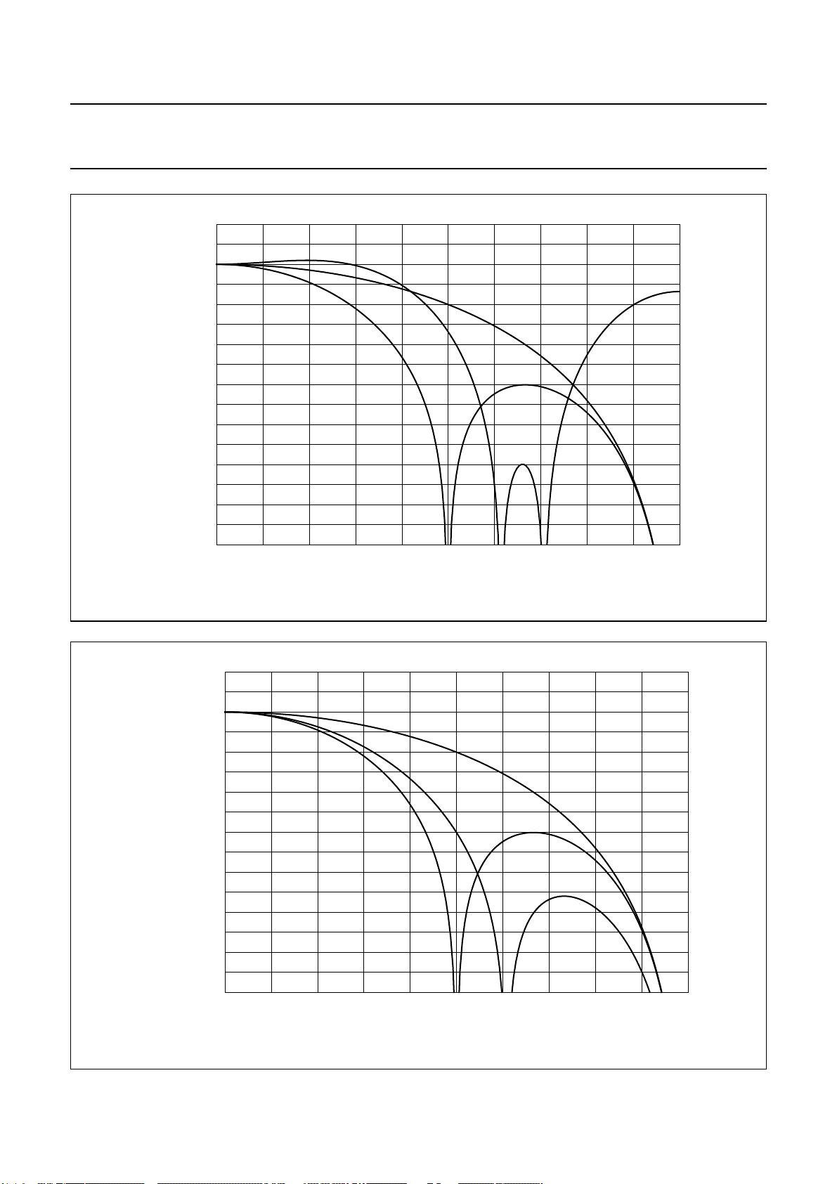
Philips Semiconductors Product specification
PAL/NTSC/SECAM video decoder with adaptive PAL/NTSC
comb filter, VBI data slicer and high performance scaler
6
V
3
(dB)
0
−3
(1) PFY[1:0] = 01.
(2) PFY[1:0] = 10.
(3) PFY[1:0] = 11.
−6
−9
−12
−15
−18
−21
−24
−27
−30
−33
−36
−39
−42
0 0.05 0.1 0.15 0.2 0.25 0.3 0.35 0.4 0.45 0.5
(3)
(1)
(2)
SAA7114
MHB543
f_sig/f_clock
(1) PFUV[1:0] = 01.
(2) PFUV[1:0] = 10.
(3) PFUV[1:0] = 11.
Fig.25 Luminance prefilter characteristic.
6
V
3
(dB)
0
−3
−6
−9
−12
−15
−18
−21
−24
−27
−30
−33
−36
−39
−42
0 0.025 0.05 0.075 0.1 0.125 0.15 0.175 0.2 0.225 0.25
(1)
(2)
(3)
f_sig/f_clock
MHB544
Fig.26 Chrominance prefilter characteristic.
2004 Mar 03 47
Page 48
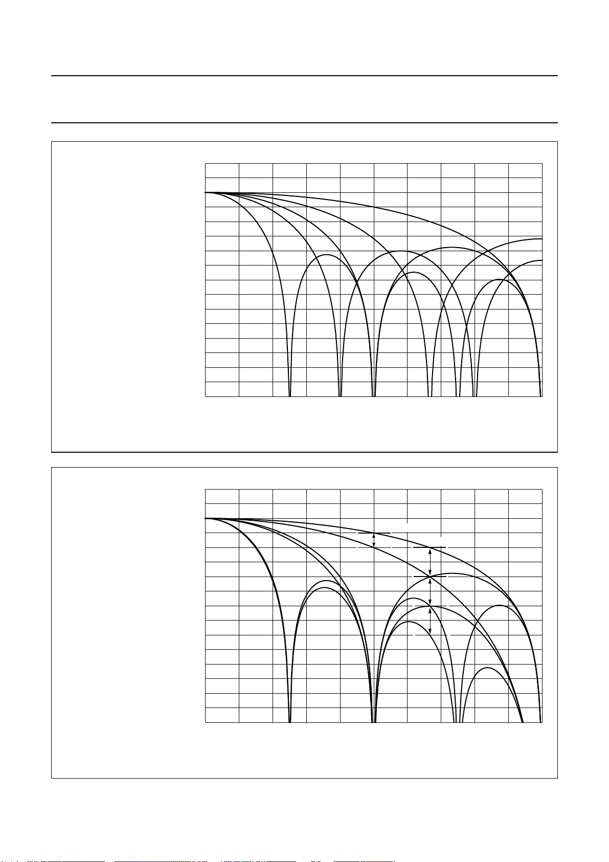
Philips Semiconductors Product specification
PAL/NTSC/SECAM video decoder with adaptive PAL/NTSC
comb filter, VBI data slicer and high performance scaler
6
V
3
(dB)
0
−3
−6
−9
−12
−15
−18
−21
−24
−27
−30
−33
−36
XC2_1 = 0; Zero’s at
×=
------------------------ XACL 1+
1
fn
with XACL = (1), (2), (3), (4) or (5)
−39
−42
0 0.05 0.1 0.15 0.2 0.25 0.3 0.35 0.4 0.45 0.5
SAA7114
MHB545
(1)(2)(3)(4)(5)
f_sig/f_clock
Fig.27 Examples for prescaler filter characteristics: effect of increasing XACL[5:0].
(1) XC2_1 = 0 and XACL[5:0] = 1.
(2) XC2_1 = 1 and XACL[5:0] = 2.
(3) XC2_1 = 0 and XACL[5:0] = 3.
(4) XC2_1 = 1 and XACL[5:0] = 4.
(5) XC2_1 = 0 and XACL[5:0] = 7.
(6) XC2_1 = 1 and XACL[5:0] = 8.
6
V
3
(dB)
0
−3
−6
−9
−12
−15
−18
−21
−24
−27
−30
−33
−36
−39
−42
0 0.05 0.1 0.15 0.2 0.25 0.3 0.35 0.4 0.45 0.5
(1)
(2)
(3)(4)(5)(6)
3 dB at 0.25
6 dB at 0.33
f_sig/f_clock
MHB546
Fig.28 Examples for prescaler filter characteristics: setting XC2_1 = 1.
2004 Mar 03 48
Page 49
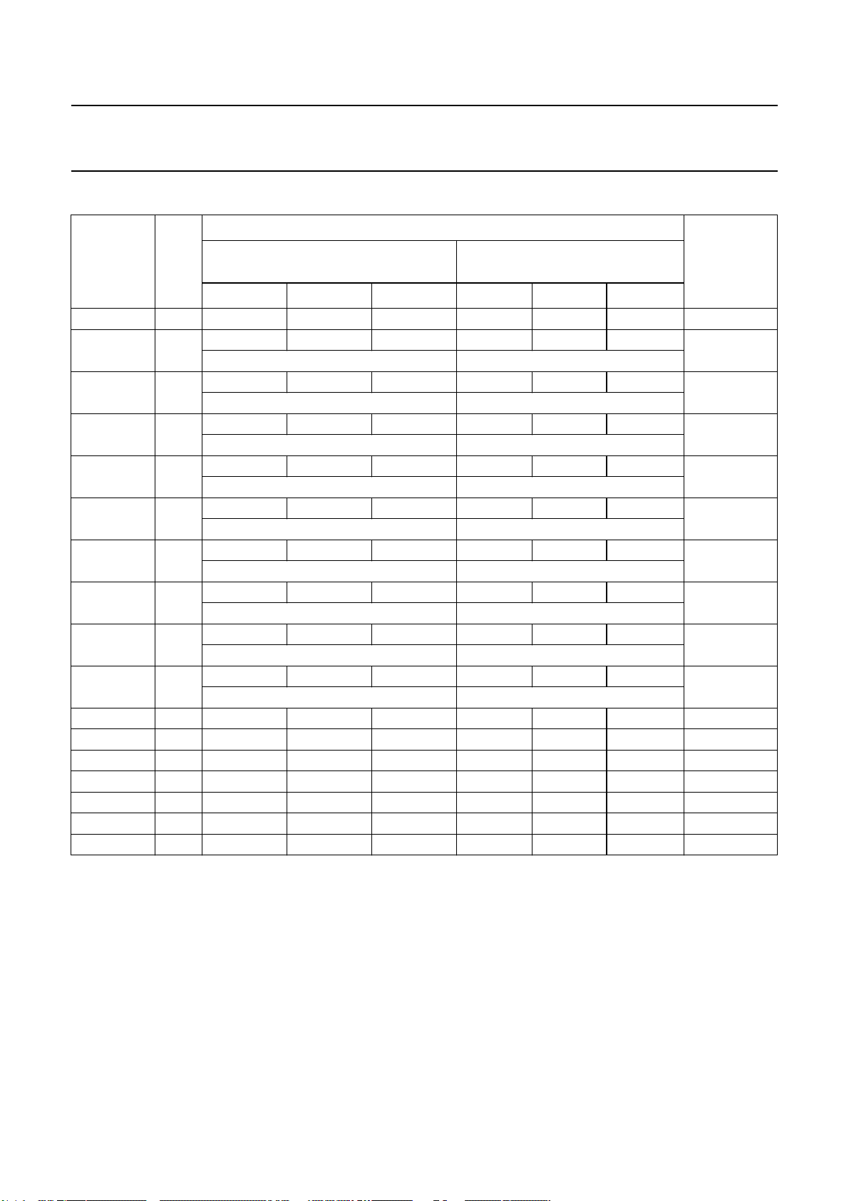
Philips Semiconductors Product specification
PAL/NTSC/SECAM video decoder with adaptive PAL/NTSC
SAA7114
comb filter, VBI data slicer and high performance scaler
Table 12 XACL[5:0] example of usage
RECOMMENDED VALUES
PRESCALE
RATIO
110 0 0 0 0 0 0to2
1
⁄
2
1
⁄
3
1
⁄
4
1
⁄
5
1
⁄
6
1
⁄
7
1
⁄
8
1
⁄
9
1
⁄
10
1
⁄
13
1
⁄
15
1
⁄
16
1
⁄
19
1
⁄
31
1
⁄
32
1
⁄
35
XPSC
[5:0]
FOR LOWER BANDWIDTH
REQUIREMENTS
FOR HIGHER BANDWIDTH
REQUIREMENTS
XACL[5:0] XC2_1 XDCG[2:0] XACL[5:0] XC2_1 XDCG[2:0]
PREFILTER
PFY[1:0]/
PFUV[1:0]
2 2 1 2 1 0 1 0 to 2
(1 2 1) ×1⁄
(1)
4
(1 1) ×1⁄
(1)
2
34 1 3 3 0 2 2
(12221)×1⁄
(1)
8
(1 1 1 1) ×1⁄
(1)
4
47 0 3 4 1 3 2
(11111111)×1⁄
(1)
8
(12221)×1⁄
(1)
8
58 1 4 7 0 3 2
(122222221)×1⁄
(1)
16
(11111111)×1⁄
(1)
8
68 1 4 7 0 3 3
(122222221)×1⁄
(1)
16
(11111111)×1⁄
(1)
8
78 1 4 7 0 3 3
(122222221)×1⁄
(1)
16
(11111111)×1⁄
(1)
8
815 0 4 8 1 4 3
(1111111111111111)×1⁄
(1)
16
(122222221)×1⁄
(1)
16
915 0 4 8 1 4 3
(1111111111111111)×1⁄
(1)
16
(122222221)×1⁄
(1)
16
10 16 1 5 8 1 4 3
(12222222222222221)×1⁄
(1)
32
(122222221)×1⁄
(1)
16
13 16 1 5 16 1 5 3
15 31 0 5 16 1 5 3
16 32 1 6 16 1 5 3
19 32 1 6 32 1 6 3
31 32 1 6 32 1 6 3
32 63 1 7 32 1 6 3
35 63 1 7 63 1 7 3
FIR
Note
1. Resulting FIR function.
2004 Mar 03 49
Page 50

Philips Semiconductors Product specification
PAL/NTSC/SECAM video decoder with adaptive PAL/NTSC
comb filter, VBI data slicer and high performance scaler
8.3.2.2 Horizontal fine scaling (variable phase delay
filter; subaddresses A8H to AFH and
D8H to DFH)
Thehorizontal fine scaling (VPD) should operateatscaling
ratios between1⁄2and 2 (0.8 and 1.6), but can also be
used for direct scaling in the range from1⁄
(theoretical) zoom 3.5 (restriction due to the internal data
path architecture), without prescaler.
In combination with the prescaler a compromise between
sharpness impression and alias can be found. This is
signal source and application dependent.
For the luminance channel a filter structure with 10 taps is
implemented, and for the chrominance a filter with 4 taps.
Luminance and chrominance scale increments
(XSCY[12:0]A9H[4:0] A8H[7:0] and XSCC[12:0] ADH[4:0]
ACH[7:0]) are defined independently, but must be set in a
2 : 1 relationship in the actual data path implementation.
The phase offsets XPHY[7:0] AAH[7:0] and XPHC[7:0]
AEH[7:0] can be used to shift the sample phases slightly.
XPHY[7:0] and XPHC[7:0] covers the phase offset range
7.999T to1⁄32T. The phase offsets should also be
programmed in a 2 : 1 ratio.
The underlying phase controlling DTO has a 13-bit
resolution.
According to the equations
Npix_in
XSCY[12:0] 1024
XSCC[12:0]
the VPD covers the scale range from 0.125 to zoom 3.5.
VPD acts equivalent to a polyphase filter with 64 possible
phases. In combination with the prescaler, it is possible to
get very accurate samples from a highly anti-aliased
integer downscaled input picture.
=
×
--------------------------- XPSC[5:0]
XSCY[12:0]
------------------------------2
×=
----------------------Npix_out
1
7.999
to
and
8.3.3.1 Line FIFO buffer (subaddresses 91H, B4H and
C1H, E4H)
The line FIFO buffer is a dual ported RAM structure for
768 pixels, with asynchronous write and read access. The
line buffer can be used for various functions, but not all
functions may be available simultaneously.
Theline buffer can buffer acompleteunscaled active video
line or more than one shorter lines (only for non-mirror
mode), for selective repetition for vertical zoom-up.
For zooming up 240 lines to 288 lines e.g., every fourth
line is requested (read) twice from the vertical scaling
circuitry for calculation.
For conversion of a 4 : 2 : 0 or 4:1:0 input sampling
scheme (MPEG, video phone, Indeo YUV-9) to ITU like
sampling scheme 4:2:2, the chrominance line buffer is
read twice or four times, before being refilled again by the
source. It has to be preserved by means of the input
acquisition window definition, so that the processing starts
with a line containing luminance and chrominance
information for 4:2:0 and 4:1:0 input. The bits
FSC[2:1] 91H[2:1] define the distance between the Y/C
lines. In the event of 4:2:2and4:1:1FSC2 and FSC1
have to be set to ‘00’.
The line buffer can also be used for mirroring, i.e. for
flippingthe image left to right, for the vanity picture invideo
phoneapplications (bit YMIR[B4H[4]]). Inmirrormode only
one active prescaled line can be held in the FIFO at a time.
The line buffer can be utilized as an excessive pipeline
buffer for discontinuous and variable rate transfer
conditions at the expansion port or image port.
SAA7114
8.3.3 VERTICAL SCALING
The vertical scaler of the SAA7114 consists of a line FIFO
bufferforline repetition and the vertical scaler block, which
implements the vertical scaling on the input data stream in
2 different operational modes from theoretical zoom by 64
down to icon size1⁄64. The vertical scaler is located
between the BCS and horizontal fine scaler, so that the
BCScan be used to compensate theDC gainamplification
of the ACM mode (see Section 8.3.3.2) as the internal
RAMs are only 8-bit wide.
2004 Mar 03 50
Page 51

Philips Semiconductors Product specification
PAL/NTSC/SECAM video decoder with adaptive PAL/NTSC
comb filter, VBI data slicer and high performance scaler
8.3.3.2 Verticalscaler (subaddresses B0H to BFH and
E0H to EFH)
Vertical scaling of any ratio from 64 (theoretical zoom)
to1⁄63 (icon) can be applied.
The vertical scaling block consists of another line delay,
and the vertical filter structure, that can operate in two
different modes; Linear Phase Interpolation (LPI) and
accumulation (ACM) mode. These are controlled by
YMODE[B4H[0]]:
• LPI mode: In LPI mode (YMODE = 0) two neighbouring
lines of the source video stream are added together, but
weighted by factors corresponding to the vertical
position (phase) of the target output line relative to the
source lines. This linear interpolation has a 6-bit phase
resolution, which equals 64 intra line phases. It
interpolates between two consecutive input lines only.
LPI mode should be applied for scaling ratios around 1
(down to1⁄2), it must be applied for vertical zooming.
• ACM mode: The vertical Accumulation (ACM) mode
(YMODE = 1) represents a vertical averaging window
over multiple lines, sliding over the field. This mode also
generates phase correct output lines. The averaging
windowlengthcorrespondstothescalingratio,resulting
in an adaptive vertical low-pass effect, to greatly reduce
aliasing artefacts. ACM can be applied for downscales
only from ratio 1 down to1⁄64. ACM results in a scale
dependent DC gain amplification, which has to be
precorrected by the BCS control of the scaler part.
The phase and scale controlling DTO calculates in 16-bit
resolution, controlled by parameters YSCY[15:0] B1H[7:0]
B0H[7:0]and YSCC[15:0]B3H[7:0] B2H[7:0], continuously
over the entire filed. A start offset can be applied to the
phase processing by means of the parameters YPY3[7:0]
to YPY0[7:0] in BFH[7:0] to BCH[7:0] and YPC3[7:0] to
YPC0[7:0]inBBH[7:0]toB8H[7:0]. The start phase covers
the range of
By programming appropriate, opposite, vertical start
phase values (subaddresses B8H to BFH and
E8H to EFH) depending on odd or even field ID of the
source video stream and A or B page cycle, frame ID
conversion and field rate conversion are supported (i.e.
de-interlacing, re-interlacing).
255
⁄32to1⁄32 lines offset.
Remark: The vertical start phase, as well as scaling
ratio are defined independently for the luminance and
chrominance channel, but must be set to the same
values in the actual implementation for accurate
4:2:2 output processing.
The vertical processing communicates on its input side
with the line FIFO buffer. The scale related equations are:
• Scaling increment calculation for ACM and LPI mode,
downscale and zoom: YSCY[15:0] and YSCC[15:0]
lower integer of= 1024
• BCS value to compensate DC gain in ACM mode
(contrast and saturation have to be set): CONT[7:0]
A5H[7:0] respectively SATN[7:0] A6H[7:0]
lower integer of
=
=
lower integer of
Nline_out
-------------------------
Nline_in
-------------------------------
YSCY[15:0]
8.3.3.3 Use of the vertical phase offsets
Asdescribed in Section 8.3.1.3, thescalerprocessing may
run randomly over the interlaced input sequence.
Additionally the interpretation and timing between ITU 656
field ID and real-time detection by means of the state of
H-sync at the falling edge of V-sync may result in different
field ID interpretation.
A vertically scaled interlaced output also gets a larger
vertical sampling phase error, if the interlaced input fields
are processed, without regard to the actual scale at the
starting point of operation (see Fig.29).
For correct interlaced processing the vertical scaler must
beused with respect to the interlace properties of the input
signal and, if required, for conversion of the field
sequences.
Four events should be considered, they are illustrated in
Fig.30.
×
1024
Nline_in
------------------------Nline_out
64×
64×
SAA7114
, or
Figures 29 and 30 and Tables 13 and 14 describe the use
of the offsets.
2004 Mar 03 51
Page 52
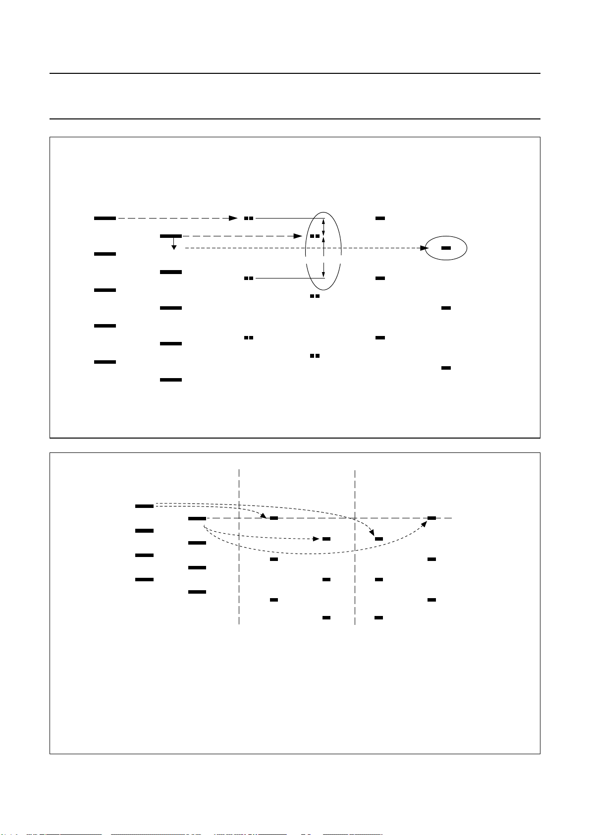
Philips Semiconductors Product specification
PAL/NTSC/SECAM video decoder with adaptive PAL/NTSC
comb filter, VBI data slicer and high performance scaler
unscaled input
field 1 field 2 field 1 field 2 field 1 field 2
scale dependent start offset
scaled output,
no phase offset
mismatched vertical line distances
scaled output,
with phase offset
correct scale dependent position
SAA7114
handbook, full pagewidth
Offset
A
B
1024
------------ 32
1
input line shift 16==
-- 2
1
input line shift
-- 2
Fig.29 Basic problem of interlaced vertical scaling (example: downscale3⁄5).
field 1 field 2
upper
B
A
32 1 line shift===
1
scale increment+
-- 2
lower
YSCY[15:0]
------------------------------ 64
field 1 field 2
case UP-UP
C
1
C
scale increment
==
-- 2
D = no offset = 0
16+==
case LO-LO
D
field 1 field 2
case UP-LO
YSCY[15:0]
------------------------------ 64
case LO-UP
MHB547
MHB548
Fig.30 Derivation of the phase related equations (example: interlace vertical scaling down to3⁄5,
with field conversion).
2004 Mar 03 52
Page 53
Philips Semiconductors Product specification
PAL/NTSC/SECAM video decoder with adaptive PAL/NTSC
comb filter, VBI data slicer and high performance scaler
In Tables 13 and 14 PHO is a usable common phase
offset.
It should be noted that the equations of Fig.30 produce an
interpolated output, also for the unscaled case, as the
geometrical reference position for all conversions is the
position of the first line of the lower field; see Table 13.
If there is no need for UP-LO and LO-UP conversion and
the input field ID is the reference for the back-end
operation, then it is UP-LO = UP-UP and LO-UP = LO-LO
and the1⁄2line phase shift (PHO + 16) that can be
skipped. This case is listed in Table 14.
The SAA7114 supports 4 phase offset registers per task
and component (luminance and chrominance). The value
of 20H represents a phase shift of one line.
Table 13 Examples for vertical phase offset usage: global equations
INPUT FIELD UNDER
PROCESSING
Upper input lines upper output lines UP-UP PHO + 16
Upper input lines lower output lines UP-LO
Lower input lines upper output lines LO-UP PHO
Lower input lines lower output lines LO-LO
OUTPUT FIELD
INTERPRETATION
USED ABBREVIATION
The registers are assigned to the following events; e.g.
subaddresses B8H to BBH:
• B8H: 00 = input field ID 0, task status bit D0 (toggle
status; see Section 8.3.1.3)
• B9H: 01 = input field ID 0, task status bit D1
• BAH: 10 = input field ID 1, task status bit D0
• BBH: 11 = input field ID 1, task status bit D1.
Depending on the input signal (interlaced or
non-interlaced) and the task processing 50 Hz or field
reduced processing with one or two tasks (see examples
in Section 8.3.1.3), other combinations may also be
possible, but the basic equations are the same.
EQUATION FOR PHASE OFFSET
CALCULATION (DECIMAL VALUES)
PHO
PHO
YSCY[15:0]
-------------------------------
YSCY[15:0]
+
-------------------------------
64
64
SAA7114
16++
2004 Mar 03 53
Page 54
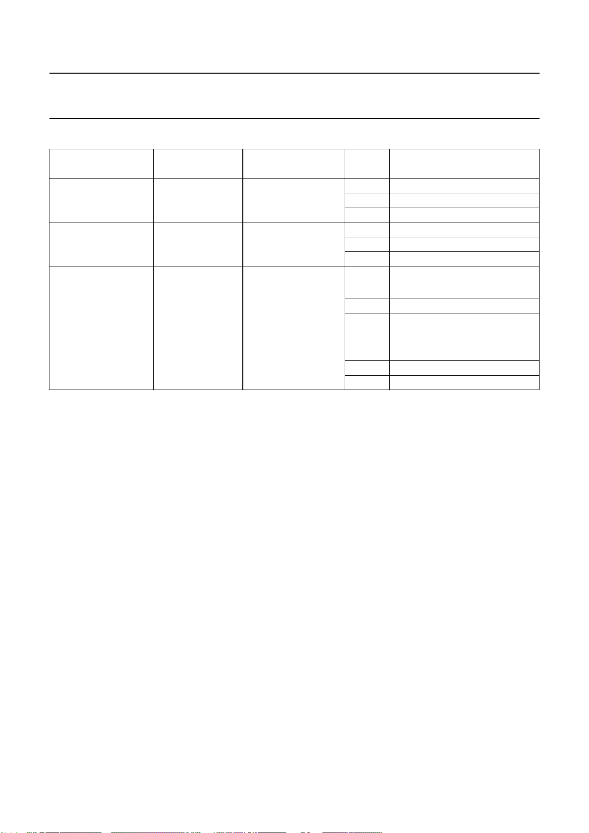
Philips Semiconductors Product specification
PAL/NTSC/SECAM video decoder with adaptive PAL/NTSC
comb filter, VBI data slicer and high performance scaler
Table 14 Vertical phase offset usage; assignment of the phase offsets
DETECTED INPUT
FIELD ID
0 = upper lines 0 YPY0[7:0] and
0 = upper lines 1 YPY1[7:0] and
1 = lower lines 0 YPY2[7:0] and
1 = lower lines 1 YPY3[7:0] and
TASK STATUS BIT
VERTICAL PHASE
OFFSET
YPC0[7:0]
YPC1[7:0]
YPC2[7:0]
YPC3[7:0]
CASE EQUATION TO BE USED
(1)
case 1
case 2
case 3
case 1 UP-UP (PHO)
case 2 UP-LO
case 3 UP-UP
case 1
case 2 LO-UP
case 3 LO-LO
case 1
case 2 LO-LO
case 3 LO-UP
UP-UP (PHO)
(2)
UP-UP
(3)
UP-LO
LO-LO
LO-LO
SAA7114
PHO
PHO
YSCY[15:0]
------------------------------64
YSCY[15:0]
------------------------------64
16–+
16–+
Notes
1. Case 1: OFIDC[90H[6]] = 0; scaler input field ID as output ID; back-end interprets output field ID at logic 0 as upper
output lines.
2. Case 2: OFIDC[90H[6]] = 1; task status bit as output ID; back-end interprets output field ID at logic 0 as upper output
lines.
3. Case 3: OFIDC[90H[6]] = 1; task status bit as output ID; back-end interprets output field ID at logic 1 as upper output
lines.
8.4 VBI data decoder and capture
(subaddresses 40H to 7FH)
The SAA7114 contains a versatile VBI data decoder.
The implementation and programming model is in
accordance with the VBI data slicer built into the
multimedia video data acquisition circuit SAA5284.
The circuitry recovers the actual clock phase during the
clock run-in period, slices the data bits with the selected
data rate, and groups them into bytes. The result is
buffered into a dedicated VBI data FIFO with a capacity of
2 × 56 bytes (2 × 14 Dwords). The clock frequency, signal
source, field frequency and accepted error count must be
defined in subaddress 40H.
The supported VBI data standards are shown in Table 15.
For lines 2 to 24 of a field, per VBI line, 1 of 16 standards
canbeselected(LCR24_[7:0]to LCR2_[7:0] in 57H[7:0] to
41H[7:0]: 23 × 2 × 4 bit programming bits).
The definition for line 24 is valid for the rest of the
corresponding field, normally no text data (video data)
should be selected there (LCR24_[7:0] = FFH) to stop the
activity of the VBI data slicer during active video.
To adjust the slicers processing to the input signal source,
there are offsets in the horizontal and vertical direction
available: parameters HOFF[10:0] 5BH[2:0] 59H[7:0],
VOFF[8:0] 5BH[4] 5AH[7:0] and FOFF[5BH[7]].
Contrary to the scalers counting, the slicers offsets define
the position of the H and V trigger events related to the
processed video field. The trigger events are the falling
edge of HREF and the falling edge of V123 from the
decoder processing part.
The relationship of these programming values to the input
signal and the recommended values are given in
Tables 5 to 8.
2004 Mar 03 54
Page 55
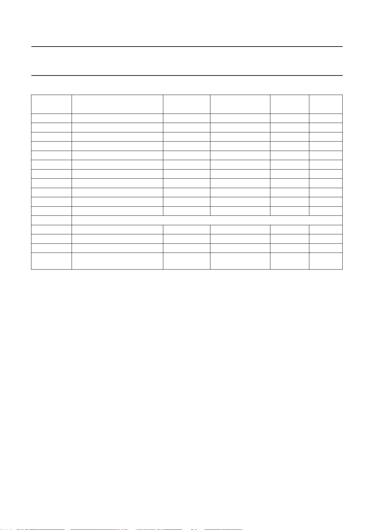
Philips Semiconductors Product specification
PAL/NTSC/SECAM video decoder with adaptive PAL/NTSC
SAA7114
comb filter, VBI data slicer and high performance scaler
Table 15 Data types supported by the data slicer block
DT[3:0]
62H[3:0]
0000 teletext EuroWST, CCST 6.9375 27H WST625 always
0001 European closed caption 0.500 001 CC625
0010 VPS 5 9951H VPS
0011 wide screen signalling bits 5 1E3C1FH WSS
0100 US teletext (WST) 5.7272 27H WST525 always
0101 US closed caption (line 21) 0.503 001 CC525
0110 (video data selected) 5 none disable
0111 (raw data selected) 5 none disable
1000 teletext 6.9375 programmable general text optional
1001 VITC/EBU time codes (Europe) 1.8125 programmable VITC625
1010 VITC/SMPTE time codes (USA) 1.7898 programmable VITC525
1011 reserved
1100 US NABTS 5.7272 programmable NABTS optional
1101 MOJI (Japanese) 5.7272 programmable (A7H) Japtext
1110 Japanese format switch (L20/22) 5 programmable open
1111 no sliced data transmitted
STANDARD TYPE
(video data selected)
DATA RATE
(Mbits/s)
5 none disable
FRAMING CODE
FC
WINDOW
HAM
CHECK
8.5 Image port output formatter
(subaddresses 84H to 87H)
The output interface consists of a FIFO for video and for
sliced text data, an arbitration circuit, which controls the
mixed transfer of video and sliced text data over the I port
and a decoding and multiplexing unit, which generates the
8 or 16-bit wide output data stream and the accompanied
reference and supporting information.
The clock for the output interface can be derived from an
internal clock, decoder, expansion port, or an externally
providedclock which is appropriate fore.g.VGA and frame
buffer.The clock can be up to 33 MHz.Thescaler provides
the following video related timing reference events
(signals), which are available on pins as defined by
subaddresses 84H and 85H:
• Output field ID
• Start and end of vertical active video range
• Start and end of active video line
• Data qualifier or gated clock
• Actually activated programming page (if CONLH is
used)
• Threshold controlled FIFO filling flags (empty, full, filled)
• Sliced data marker.
The discontinuous data stream at the scaler output is
accompanied by a data valid flag (or data qualifier), or is
transported via a gated clock. Clock cycles with invalid
dataon the I port data bus (including the HPD pinsin16-bit
output mode) are marked with code 00H.
The output interface also arbitrates the transfer between
scaled video data and sliced text data over the I port
output.
The bits VITX1 and VITX0 (subaddress 86H) are used to
control the arbitration.
Asafurther operation the serialization of the internal 32-bit
Dwords to 8-bit or optional 16-bit output, as well as the
insertion of the extended ITU 656 codes (SAV/EAV for
video data, ANC or SAV/EAV codes for sliced text data)
are done here.
For handshake with the VGA controller, or other memory
or bus interface circuitry, programmable FIFO flags are
provided; see Section 8.5.2.
2004 Mar 03 55
Page 56
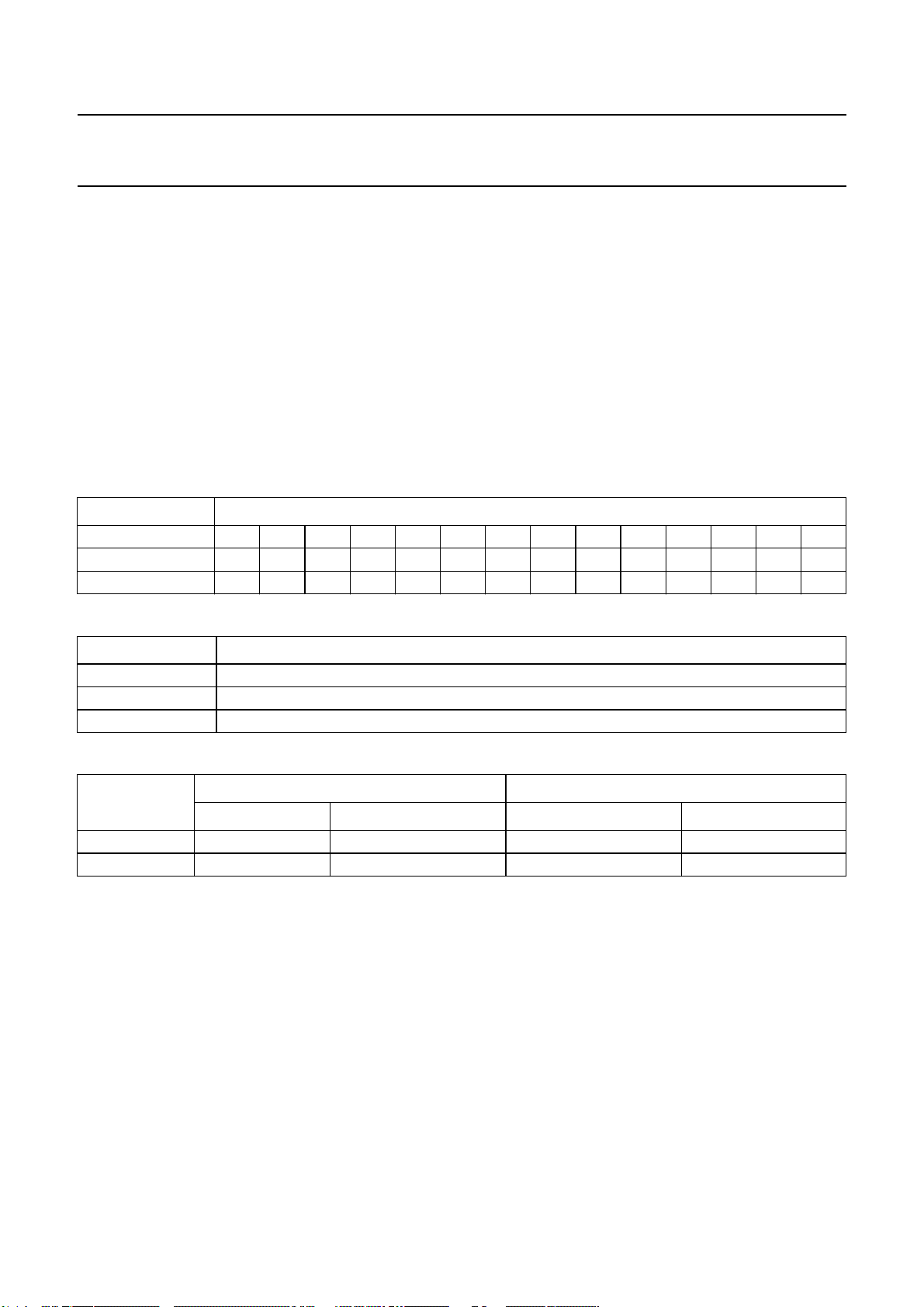
Philips Semiconductors Product specification
PAL/NTSC/SECAM video decoder with adaptive PAL/NTSC
SAA7114
comb filter, VBI data slicer and high performance scaler
8.5.1 SCALER OUTPUT FORMATTER
(SUBADDRESSES 93H AND C3H)
The output formatter organizes the packing into the output
FIFO. The following formats are available:
Y-CB-CR4:2:2, Y-CB-CR4:1:1, Y-CB-CR4:2:0,
Y-CB-CR4:1:0 and Yonly (e.g. for raw samples). The
formatting is controlled by FSI[2:0] 93H[2:0], FOI[1:0]
93H[4:3] and FYSK[93H[5]].
The data formats are defined on Dwords,or multiples, and
are similar to the video formats as recommended for PCI
multimedia applications (compares to SAA7146A), but
planar formats are not supported.
Table 16 Byte stream for different output formats
OUTPUT FORMAT BYTE SEQUENCE FOR 8-BIT OUTPUT MODES
Y-CB-CR4:2:2 CB0Y0 CR0Y1 CB2Y2 CR2Y3 CB4Y4 CR4Y5 CB6Y6
Y-CB-CR4:1:1 CB0Y0 CR0Y1 CB4Y2 CR4Y3Y4Y5Y6Y7CB8Y8
Yonly Y0 Y1 Y2 Y3 Y4 Y5 Y6 Y7 Y8 Y9 Y10 Y11 Y12 Y13
FSI[2:0] defines the horizontal packing of the data,
FOI[1:0] defines how many Y only lines are expected,
before a Y/C line will be formatted. If FYSK is set to logic 0
preceding Y only lines will be skipped, and the output will
always start with a Y/C line.
Additionallythe output formatter limits the amplitude range
of the video data (controlled by ILLV[85H[5]]); see
Table 18.
Table 17 Explanation to Table 16
NAME EXPLANATION
CBnC
Yn Y (luminance) component, pixel number n = 0, 1, 2, 3 to 719
CRnC
Table 18 Limiting range on I port
LIMIT STEP
ILLV[85H[5]]
0 1 to 254 01 to FE 00 FF
1 8 to 247 08 to F7 00 to 07 F8 to FF
8.5.2 VIDEO FIFO (SUBADDRESS 86H)
The video FIFO at the scaler output contains 32 Dwords.
That corresponds to 64 pixels in 16-bit Y-CB-CR 4:2:2
format.Butasthe entire scaler can act as a pipeline buffer,
the actual available buffer capacity for the image port is
much higher, and can exceed beyond a video line.
The image port, and the video FIFO, can operate with the
video source clock (synchronous mode) or with an
externally provided clock (asynchronous and burst mode),
as appropriate for the VGA controller or attached frame
buffer.
The video FIFO provides 4 internal flags, reporting to what
extent the FIFO is actually filled.
(B − Y) colour difference component, pixel number n = 0, 2, 4 to 718
B
(R − Y) colour difference component, pixel number n= 0, 2, 4 to 718
R
VALID RANGE SUPPRESSED CODES (HEXADECIMAL VALUE)
DECIMAL VALUE HEXADECIMAL VALUE LOWER RANGE UPPER RANGE
These are:
• The FIFO Almost Empty (FAE) flag
• The FIFO Combined Flag (FCF) or FIFO filled, which is
set at almost full level and reset, with hysteresis, only
after the level crosses below the almost empty mark
• The FIFO Almost Full (FAF) flag
• The FIFO Overflow (FOVL) flag.
The trigger levels for FAE and FAF are programmable by
FFL[1:0] 86H[3:2] (16, 24, 28, full) and FEL[1:0] 86H[1:0]
(16, 8, 4, empty).
The state of this flag can be seen on the pins IGP0 or
IGP1. The pin mapping is defined by subaddresses
84H and 85H; see Section 9.5.
2004 Mar 03 56
Page 57

Philips Semiconductors Product specification
PAL/NTSC/SECAM video decoder with adaptive PAL/NTSC
comb filter, VBI data slicer and high performance scaler
8.5.3 TEXT FIFO
The data of the internal VBI data slicer is collected in the
text FIFO before the transmission over the I port is
requested (normally before the video window starts). It is
partitioned into two FIFO sections. A complete line is filled
into the FIFO before a data transfer is requested.
So normally, one line of text data is ready for transfer,
while the next text line is collected. Thus sliced text data is
delivered as a block of qualified data, without any
qualification gaps in the byte stream of the I port.
The decoded VBI data is collected in the dedicated VBI
data FIFO. After the capture of a line has been completed,
the FIFO can be streamed through the image port,
preceded by a header, giving line number and standard.
The VBI data period can be signalled via the sliced data
flag on pin IGP0 or IGP1. The decoded VBI data is lead by
the ITU ancillary data header (DID[5:0] 5DH[5:0] at value
<3EH) or by SAV/EAV codes selectable by DID[5:0] at
value 3EH or 3FH. Pin IGP0 or IGP1 is set if the first byte
of the ANC header is valid on the I port bus. It is reset if an
SAV occurs. So it may frame multiple lines of text data
output, in the event that the video processing starts with a
distance of several video lines to the region of text data.
Valid sliced data from the text FIFO is available on the
I port as long as the IGP0 or IGP1 flag is set and the data
qualifier is active on pin IDQ.
The decoded VBI data is presented in two different data
formats, controlled by bit RECODE.
• RECODE = 1: values 00H and FFH will be recoded to
even parity values 03H and FCH
• RECODE = 0: values 00H and FFH may occur in the
data stream as detected.
Ifthe video data is transferred without any interrupt and the
video FIFO does not need to buffer any output pixel, the
text data is inserted after the end of a scaled video line,
normally during the blanking interval of the video.
8.5.5 DATA STREAM CODING AND REFERENCE SIGNAL
GENERATION (SUBADDRESSES 84H, 85H AND 93H)
As H and V reference signals are logic 1, active gate
signalsaregenerated,whichframe the transfer of the valid
output data. As an alternative to the gates, H and V trigger
pulses are generated on the rising edges of the gates.
Dueto the dynamic FIFO behaviour of thecomplete scaler
path, the output signal timing has no fixed timing
relationship to the real-time input video stream. So fixed
propagation delays, in terms of clock cycles, related to the
analog input cannot be defined.
The data stream is accompanied by a data qualifier.
Additionally invalid data cycles are marked with code 00H.
If ITU 656 like codes are not required, they can be
suppressed in the output stream.
As a further option, it is possible to provide the scaler with
an external gating signal on pin ITRDY. Thereby making it
possible to hold the data output for a certain time and to
get valid output data in bursts of a guaranteed length.
The sketched reference signals and events can be
mapped to the I port output pins IDQ, IGPH, IGPV, IGP0
and IGP1. For flexible use the polarities of all the outputs
can be modified. The default polarity for the qualifier and
reference signals is logic 1 (active).
Table 19 shows the relevant and supported SAV and EAV
coding.
SAA7114
8.5.4 VIDEO AND TEXT ARBITRATION (SUBADDRESS 86H)
Slicedtext data and scaled video data aretransferred over
the same bus, the I port. The mixed transfer is controlled
by an arbitration circuit.
2004 Mar 03 57
Page 58
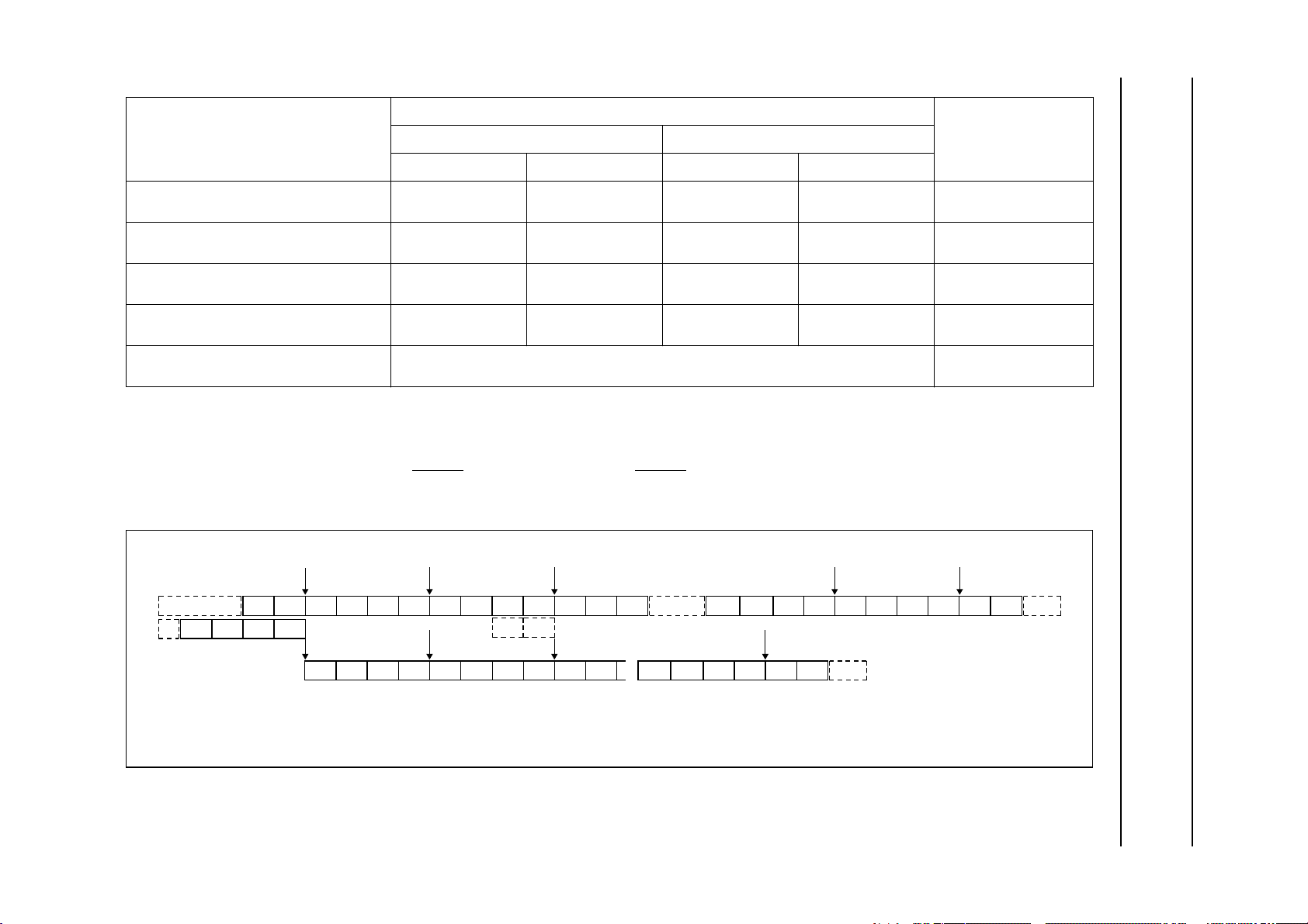
This text is here in white to force landscape pages to be rotated correctly when browsing through the pdf in the Acrobat reader.This text is here in
_white to force landscape pages to be rotated correctly when browsing through the pdf in the Acrobat reader.This text is here inThis text is here in
white to force landscape pages to be rotated correctly when browsing through the pdf in the Acrobat reader. white to force landscape pages to be ...
2004 Mar 03 58
Table 19 SAV/EAV codes on I port
(1)
(HEX)
(2)
OF SAV/EAV BYTE = 1
COMMENTMSB
EVENT DESCRIPTION
SAV/EAV CODES ON I PORT
(2)
OF SAV/EAV BYTE = 0 MSB
FIELD ID = 0 FIELD ID = 1 FIELD ID = 0 FIELD ID = 1
Next pixel is FIRST pixel of any active
line
Previous pixel was LAST pixel of any
active line, but not the last
Next pixel is FIRST pixel of any
V-blanking line
Previous pixel was LAST pixel of the
last active line or of any V-blanking line
No valid data, don’t capture and don’t
0E 49 80 C7 HREF = active;
VREF = active
13 54 9D DA HREF = inactive;
VREF = active
25 62 AB EC HREF = active;
VREF = inactive
38 7F B6 F1 HREF = inactive;
VREF = inactive
00 IDQ pin inactive
increment pointer
Notes
1. The leading byte sequence is: FFH-00H-00H.
2. The MSB of the SAV/EAV code byte is controlled by:
a) Scaler output data: task A ⇒ MSB = CONLH[90H[7]]; task B ⇒ MSB = CONLH[C0H[7]].
b) VBI data slicer output data: DID[5:0] 5DH[5:0] = 3EH ⇒ MSB = 1; DID[5:0] 5DH[5:0] = 3FH ⇒ MSB = 0.
Philips Semiconductors Product specification
PAL/NTSC/SECAM video decoder with adaptive PAL/NTSC
comb filter, VBI data slicer and high performance scaler
invalid data
or
end of raw VBI line
00 00 FF 00 00 SAV SDID DC IDI1 IDI2 D
...
FF 00 00 EAV
ANC header active for DID (subaddress 5DH) <3EH
timing reference code
ANC header internal header sliced data
00 FF FF DID SDID DC IDI1 IDI2 D
sliced data invalid dataand filling data
1_3D1_4D2_1
D
D
1_2
1_1
1_3D1_4
D
DC_3DDC_4
D
DC_3DDC_4
CS BC 00 00...
Fig.31 Sliced data formats on the I port in 8-bit mode.
timing reference codeinternal header
CS BC FF 00 00 EAV 00 00... ...
ANC data output is only filled up
to the Dword boundary
...
...
MHB549
SAA7114
Page 59

Philips Semiconductors Product specification
PAL/NTSC/SECAM video decoder with adaptive PAL/NTSC
SAA7114
comb filter, VBI data slicer and high performance scaler
Table 20 Explanation to Fig.31
NAME EXPLANATION
SAV start of active data; see Table 21
(1)
SDID sliced data identification: NEP
5EH, D5 to D0, e. g. to be used as source identifier
(1)
DC Dword count: NEP
(2)
, EP
, DC5 to DC0. DC describes the number of succeeding 32-bit words:
• For SAV/EAV mode DC is fixed to 11 Dwords (byte value 4BH)
• For ANC mode it is: DC =1⁄4(C + n), where C = 2 (the two data identification bytes IDI1 and IDI2) and
n = number of decoded bytes according to the chosen text standard.
It should be noted that the number of valid bytes inside the stream can be seen in the BC byte.
IDI1 internal data identification 1: OP
LineNumber8 to LineNumber3 = Dword 1 byte 1; see Table 21
IDI2 internal data identification 2: OP
DataType3 to DataType0 = Dword 1 byte 2; see Table21
D
D
n_m
DC_4
Dword number n, byte number m
last Dword byte 4, note: for SAV/EAV framing DC is fixed to 0BH, missing data bytes are filled up; the fill
value is A0H
CS the check sum byte, the check sum is accumulated from the SAV (respectively DID) byte to the D
BC number of valid sliced bytes counted from the IDI1 byte
EAV end of active data; see Table 21
(2)
, EP
, SDID5 to SDID0, freely programmable via I2C-bus subaddress
(3)
, FID (field 1 = 0, field 2 = 1),
(3)
, LineNumber2 to LineNumber0,
DC_4
byte
Notes
1. Inverted EP (bit D7); for EP see note 2.
2. Even parity (bit D6) of bits D5 to D0.
3. Odd parity (bit D7) of bits D6 to D0.
2004 Mar 03 59
Page 60
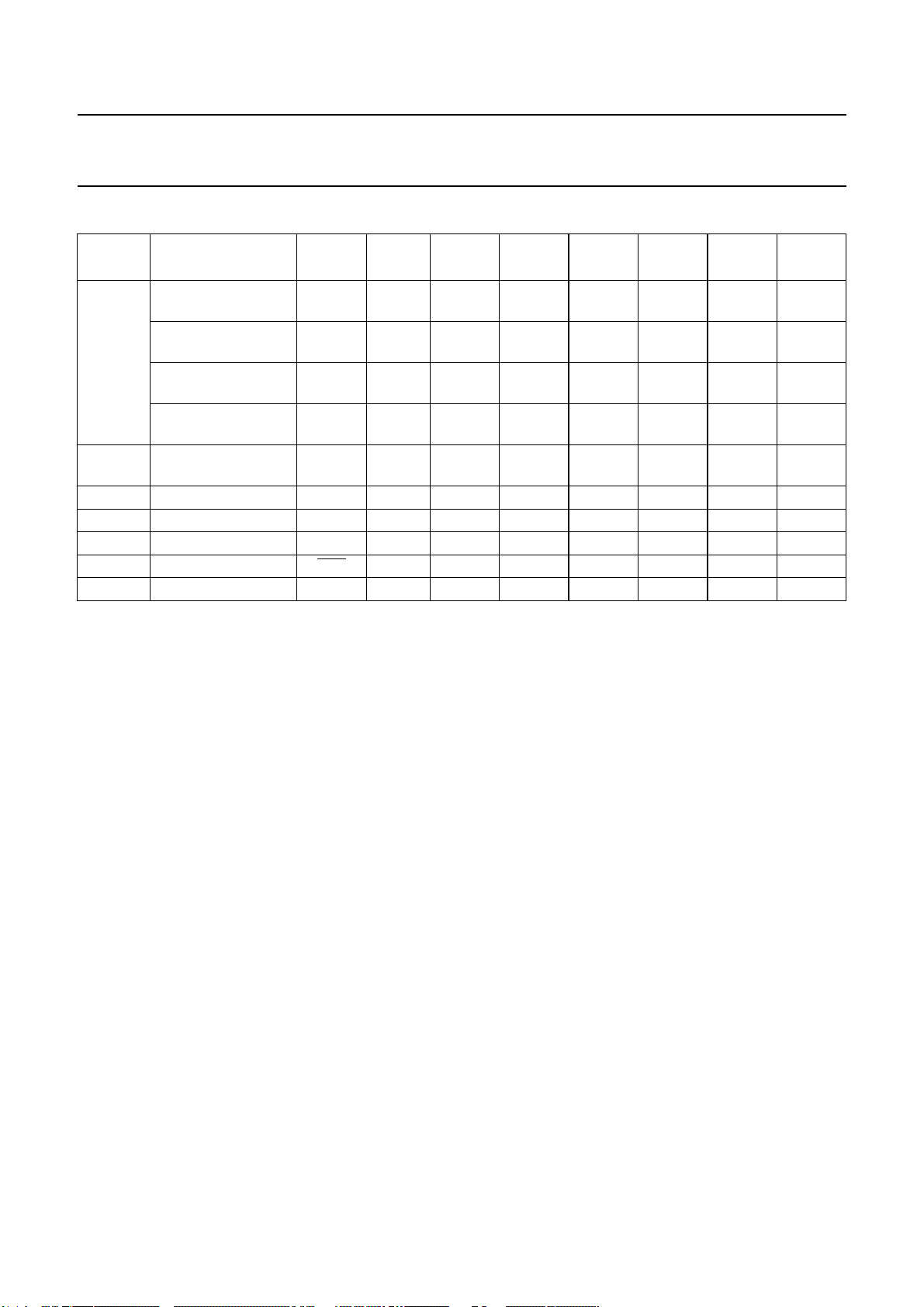
Philips Semiconductors Product specification
PAL/NTSC/SECAM video decoder with adaptive PAL/NTSC
SAA7114
comb filter, VBI data slicer and high performance scaler
Table 21 Bytes stream of the data slicer
NICK
NAME
DID,
SAV,
EAV
SDID programmable via
(8)
DC
IDI1 OP
IDI2 OP
CS check sum byte CS6 CS6 CS5 CS4 CS3 CS2 CS1 CS0
BC valid byte count OP
COMMENT D7 D6 D5 D4 D3 D2 D1 D0
subaddress
NEP
(1)
EP
(2)
0 1 0 FID
(3)
(4)
I1
5DH = 00H
subaddress 5DH;
NEP
(1)
EP
(2)
0 D4[5DH] D3[5DH] D2[5DH] D1[5DH] D0[5DH]
D5=1
subaddress 5DH
1 FID
(3)
(6)
V
(7)
H
P3 P2 P1 P0
D5 = 3EH; note 5
subaddress 5DH
0 FID
(3)
(6)
V
(7)
H
P3 P2 P1 P0
D5 = 3FH; note 5
NEP
(1)
EP
(2)
D5[5EH] D4[5EH] D3[5EH] D2[5EH] D1[5EH] D0[5EH]
subaddress 5EH
NEP
(1)
(9)
(9)
(9)
(2)
EP
FID
LN2
(3)
(10)
DC5 DC4 DC3 DC2 DC1 DC0
LN8
LN1
(10)
(10)
LN7
LN0
(10)
(10)
LN6
DT3
(10)
(11)
LN5
DT2
(10)
(11)
LN4
DT1
(10)
(11)
0 CNT5 CNT4 CNT3 CNT2 CNT1 CNT0
I0
LN3
DT0
(4)
(10)
(11)
Notes
1. NEP = inverted EP (see note 2).
2. EP = Even Parity of bits D5 to D0.
3. FID = 0: field 1; FID = 1: field 2.
4. I1 = 0 and I0 = 0: before line 1; I1 = 0 and I0 = 1: lines 1 to 23; I1 = 1 and I0 = 0: after line 23; I1 = 1 and I0 = 1:
line 24 to end of field.
5. Subaddress 5DH at 3EH and 3FH are used for ITU 656 like SAV/EAV header generation; recommended value.
6. V = 0: active video; V = 1: blanking.
7. H = 0: start of line; H = 1: end of line.
8. DC = Data Count in Dwords according to the data type.
9. OP = Odd Parity of bits D6 to D0.
10. LN = Line Number.
11. DT = Data Type according to table.
2004 Mar 03 60
Page 61
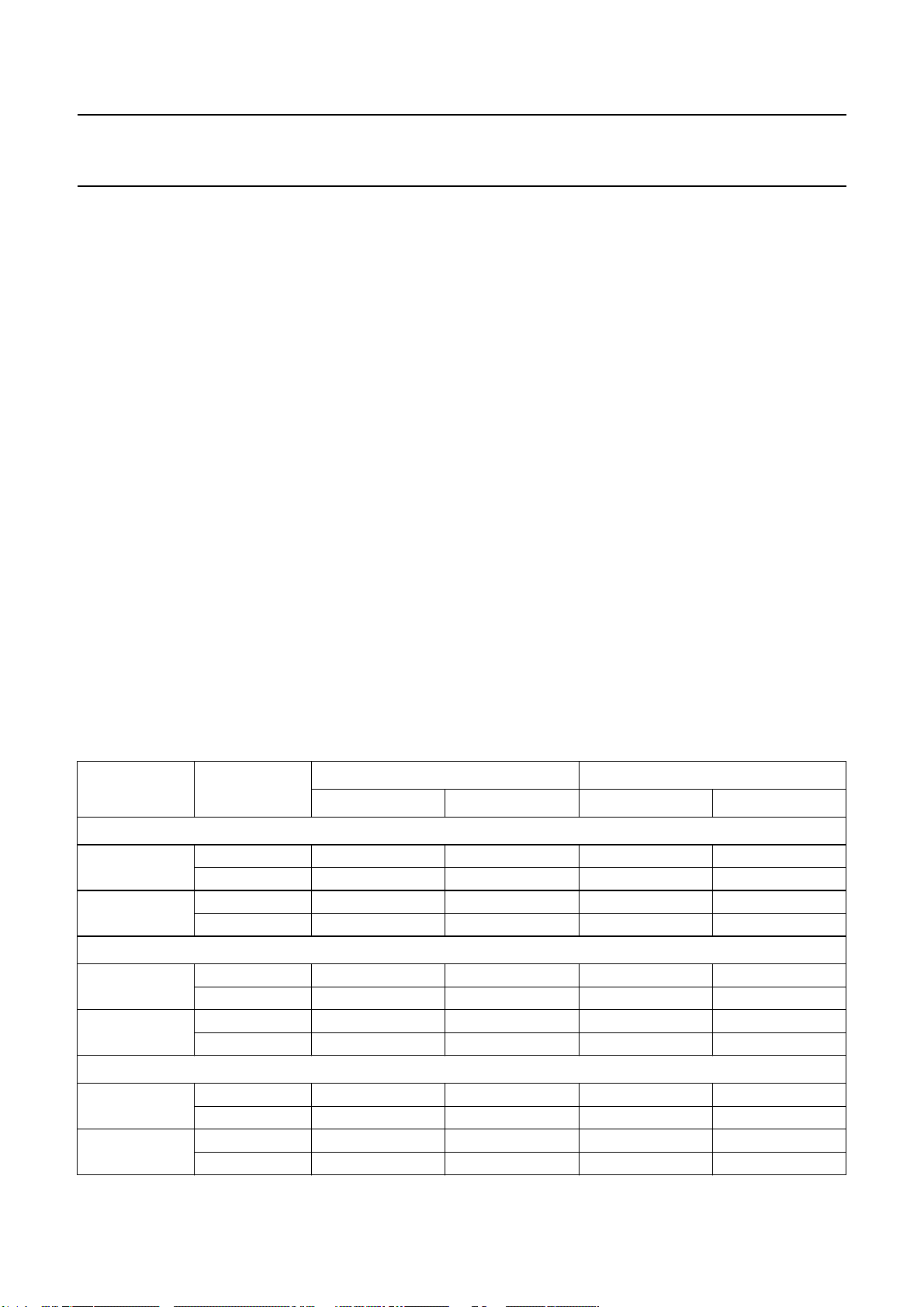
Philips Semiconductors Product specification
PAL/NTSC/SECAM video decoder with adaptive PAL/NTSC
comb filter, VBI data slicer and high performance scaler
8.6 Audio clock generation
(subaddresses 30H to 3FH)
TheSAA7114 incorporates the generationofa field-locked
audio clock as an auxiliary function for video capture. An
audio sample clock, that is locked to the field frequency,
ensures that there is always the same predefined number
of audio samples associated with a field, or a set of fields.
This ensures synchronous playback of audio and video
after digital recording (e.g. capture to hard disk), MPEG or
other compression, or non-linear editing.
8.6.1 MASTER AUDIO CLOCK
The audio clock is synthesized from the same crystal
frequency as the line-locked video clock is generated. The
master audio clock is defined by the parameters:
• Audio master Clocks Per Field, ACPF[17:0] 32H[1:0]
31H[7:0] 30H[7:0] according to the equation:
audio frequency
ACPF[17:0] round
=
------------------------------------------
field frequency
Remark: For standard applications the synthesized audio
clock AMCLK can be used directly as master clock and as
input clock for port AMXCLK (short cut) to generate
ASCLK and ALRCLK. For high-end applications it is
recommended to use an external analog PLL circuit to
enhance the performance of the generated audio clock.
SAA7114
• Audio master Clocks Nominal Increment, ACNI[21:0]
36H[5:0] 35H[7:0] 34H[7:0] according to the equation:
audio frequency
ACNI[21:0] round
See Table 22 for examples.
Table 22 Programming examples for audio master clock generation
XTALO
(MHz)
AMCLK = 256 × 48 kHz (12.288 MHz)
32.11
24.576
AMCLK = 256 × 44.1 kHz (11.2896 MHz)
32.11
24.576
AMCLK = 256 × 32 kHz (8.192 MHz)
32.11
24.576
=
---------------------------------------------
crystal frequency
FIELD
(Hz)
50 245760 3C000 3210190 30FBCE
59.94 205005 320CD 3210190 30FBCE
50 −−−−
59.94 −−−−
50 225792 37200 2949362 2D00F2
59.94 188348 2DFBC 2949362 2D00F2
50 225792 37200 3853517 3ACCCD
59.94 188348 2DFBC 3853517 3ACCCD
50 163840 28000 2140127 20A7DF
59.94 136670 215DE 2140127 20A7DF
50 163840 28000 2796203 2AAAAB
59.94 136670 215DE 2796203 2AAAAB
23
×
2
ACPF ACNI
DECIMAL HEX DECIMAL HEX
2004 Mar 03 61
Page 62
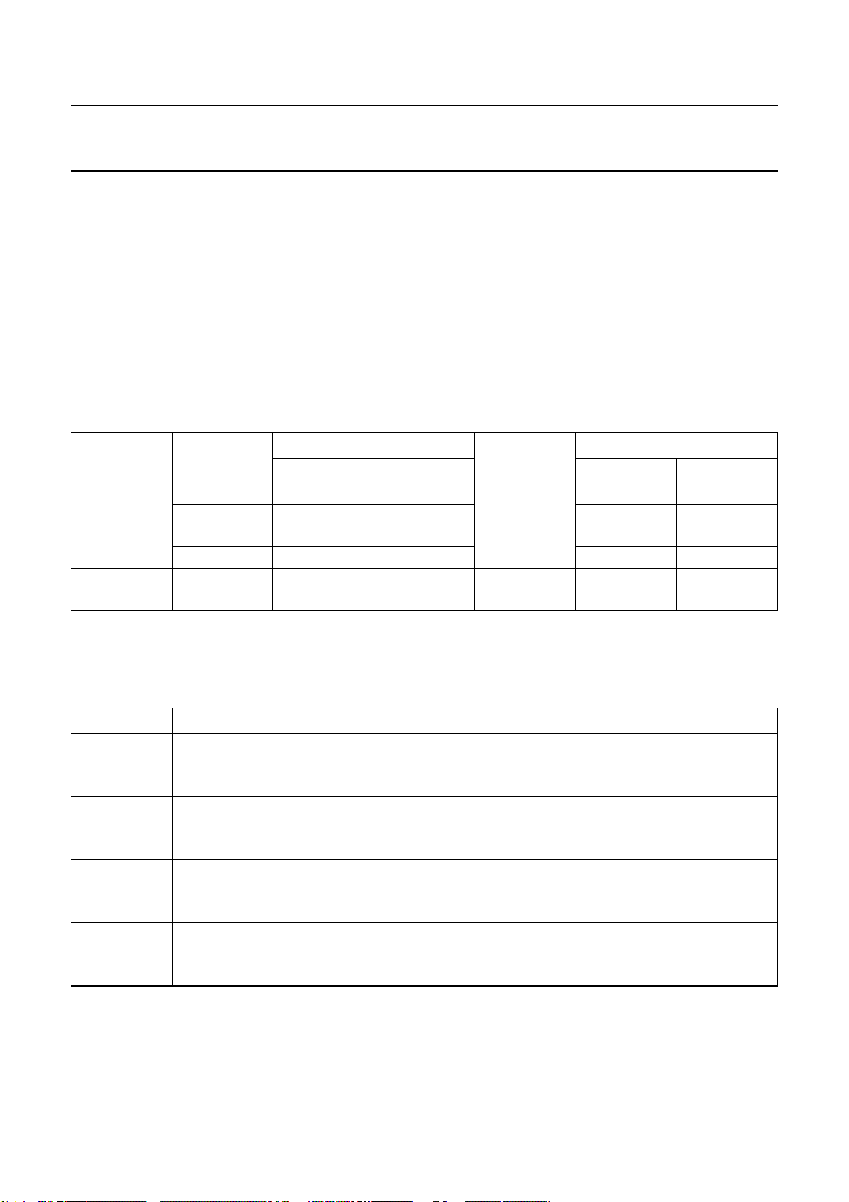
Philips Semiconductors Product specification
PAL/NTSC/SECAM video decoder with adaptive PAL/NTSC
SAA7114
comb filter, VBI data slicer and high performance scaler
8.6.2 SIGNALS ASCLK AND ALRCLK
Two binary divided signals ASCLK and ALRCLK are provided for slower serial digital audio signal transmission and for
channel-select. The frequencies of these signals are defined by the following parameters:
• SDIV[5:0] 38H[5:0] according to the equation:
f
f
ASCLK
AMXCLK
= SDIV[5:0]
------------------------------------- SDIV 1+()2×
⇒
• LRDIV[5:0] 39H[5:0] according to the equation: ⇒
See Table 23 for examples.
Table 23 Programming examples for ASCLK/ALRCLK clock generation
AMXCLK
(MHz)
12.288
11.2896
8.192
ASCLK
(kHz)
DECIMAL HEX DECIMAL HEX
1536 3 03
768 7 07 8 08
1411.2 3 03
2822.4 1 01 32 10
1024 3 03
2048 1 01 32 10
f
AMXCLK
-------------------2f
ASCLK
f
SDIV
1–=
ALRCLK
f
ASCLK
= LRDIV[5:0]
-------------------------- LRDIV 2×
ALRCLK
(kHz)
48
44.1
32
f
ASCLK
=
---------------------- 2f
ALRCLK
LRDIV
16 10
16 10
16 10
8.6.3 OTHER CONTROL SIGNALS
Further control signals are available to define reference clock edges and vertical references; see Table 24.
Table 24 Control signals for reference clock edges and vertical references
SIGNAL DESCRIPTION
APLL[3AH[3]] Audio PLL mode
0 = PLL closed
1 = PLL open
AMVR[3AH[2]] Audio Master clock Vertical Reference
0 = internal V
1 = external V
LRPH[3AH[1]] ALRCLK phase
0 = invert ASCLK, ALRCLK edges triggered by falling edge of ASCLK
1 = don’t invert ASCLK, ALRCLK edges triggered by rising edge of ASCLK
SCPH[3AH[0]] ASCLK phase
0 = invert AMXCLK, ASCLK edges triggered by falling edge of AMXCLK
1 = don’t invert AMXCLK, ASCLK edges triggered by rising edge of AMXCLK
2004 Mar 03 62
Page 63

Philips Semiconductors Product specification
PAL/NTSC/SECAM video decoder with adaptive PAL/NTSC
SAA7114
comb filter, VBI data slicer and high performance scaler
9 INPUT/OUTPUT INTERFACES AND PORTS
The SAA7114 has 5 different I/O interfaces:
• Analog video input interface, for analog CVBS and/or
Y and C input signals
• Audio clock port
• Digital real-time signal port (RT port)
• Digitalvideo expansion port (X port), for unscaled digital
video input and output
• Digital image port (I port) for scaled video data output
and programming
• Digital host port (H port) for extension of the image port
or expansion port from 8 to 16-bit.
Table 25 Analog pin description
SYMBOL PIN
AI24 to AI21 P6, P7, P9 and P10
(10, 12, 14 and 16)
AI12 and AI11 P11 and P13
AOUT M10 (22) O analog video output, for test purposes AOSL1 and AOSL0
AI1D and AI2D P12 and P8
(1)
(18 and 20)
(19 and 13)
I/O DESCRIPTION BIT
I analog video signal inputs, e.g. 2 CVBS signals and
two Y/C pairs can be connected simultaneously
I analog reference pins for differential ADC operation −
9.1 Analog terminals
The SAA7114 has 6 analog inputs AI21 to AI24, AI11 and
AI12 for composite video CVBS or S-video Y/C signal
pairs. Additionally, there are two differential reference
inputs, which must be connected to ground via a capacitor
equivalent to the decoupling capacitors at the 6 inputs.
There are no peripheral components required other than
these decoupling capacitors and 18 Ω/56 Ω termination
resistors, one set per connected input signal; see
application example in Fig.41. Two anti-alias filters are
integrated, and self adjusting via the clock frequency.
Clamp and gain control for the two ADCs are also
integrated. An analog video output (pin AOUT) is provided
for testing purposes.
MODE3 to MODE0
Note
1. Pin numbers for LQFP100 in parenthesis.
2004 Mar 03 63
Page 64
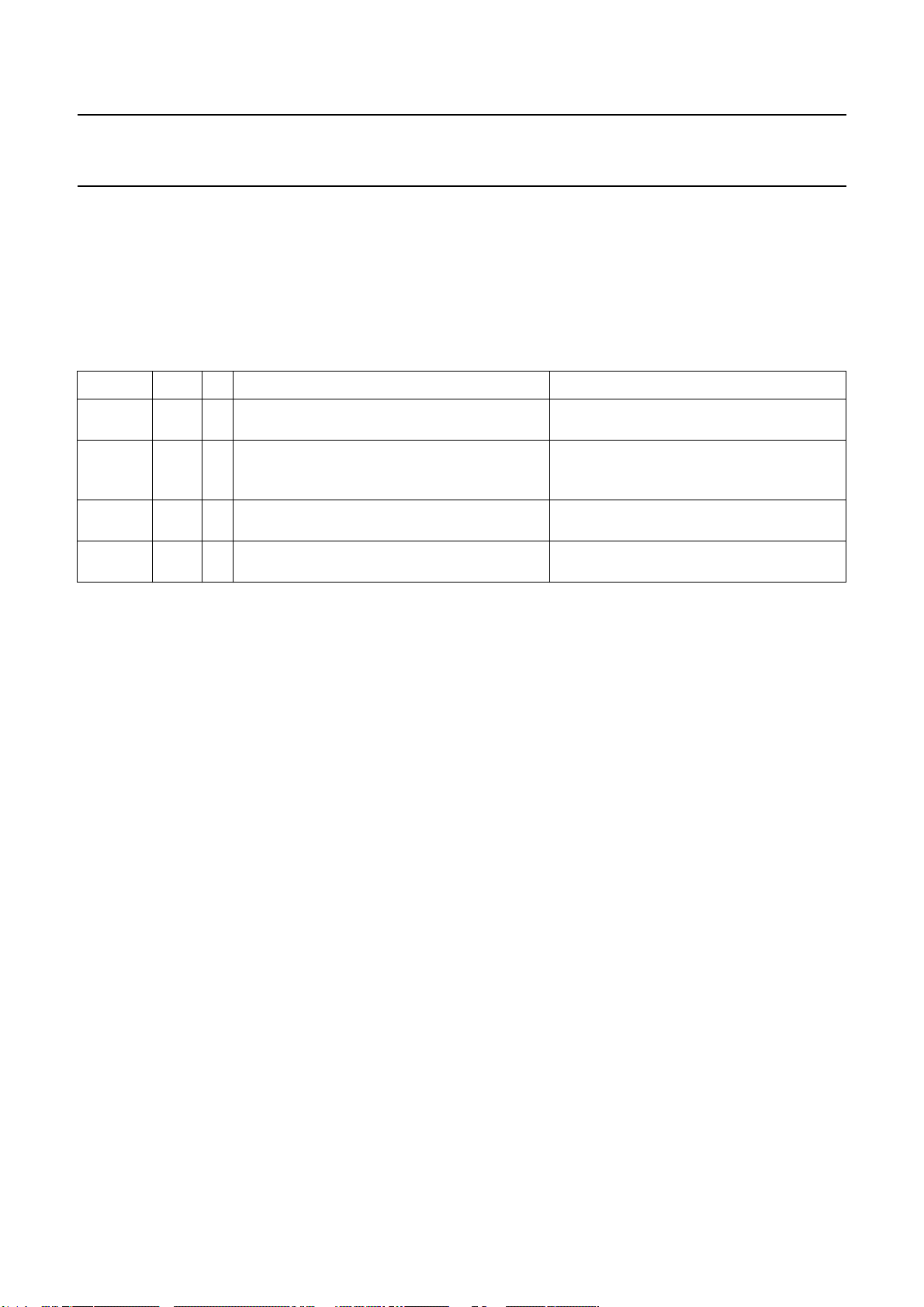
Philips Semiconductors Product specification
PAL/NTSC/SECAM video decoder with adaptive PAL/NTSC
comb filter, VBI data slicer and high performance scaler
9.2 Audio clock signals
The SAA7114 also synchronizes the audio clock and
sampling rate to the video frame rate, via a very slow PLL.
Thisensures that the multimediacaptureand compression
processes always gather the same predefined number of
samples per video frame.
Table 26 Audio clock pin description
SYMBOL PIN
AMCLK K12
AMXCLK J12
ASCLK K14
ALRCLK J13
(1)
I/O DESCRIPTION BIT
O audio master clock output ACPF[17:0] 32H[1:0] 31H[7:0] 30H[7:0] and
(37)
I external audio master clock input for the clock
(41)
(39)
(40)
division circuit, can be directly connected to
output AMCLK for standard applications
O serial audio clock output, can be synchronized
to rising or falling edge of AMXCLK
O audio channel (left/right) clock output, can be
synchronized to rising or falling edge of ASCLK
An audio master clock AMCLK and two divided clocks
ASCLK and ALRCLK are generated:
• ASCLK: can be used as audio serial clock
• ALRCLK: audio left/right channel clock.
The ratios are programmable; see Section 8.6.
ACNI[21:0] 36H[5:0] 35H[7:0] 34H[7:0]
−
SDIV[5:0] 38H[5:0] and SCPH[3AH[0]]
LRDIV[5:0] 39H[5:0] and LRPH[3AH[1]]
SAA7114
Note
1. Pin numbers for LQFP100 in parenthesis.
9.3 Clock and real-time synchronization signals
For the generation of the line-locked video (pixel) clock
LLC, and of the frame-locked audio serial bit clock, a
crystal accurate frequency reference is required. An
oscillator is built-in for fundamental or third harmonic
crystals. The supported crystal frequencies are
32.11 or 24.576 MHz (defined during reset by strapping
pin ALRCLK).
Alternatively pin XTALI can be driven from an external
single-ended oscillator.
The crystal oscillation can be propagated as a clock to
other ICs in the system via pin XTOUT.
The Line-Locked Clock (LLC) is the double pixel clock of
nominal 27 MHz. It is locked to the selected video input,
generating baseband video pixels according to
recommendation 601”
circuits, a direct pixel clock (LLC2) is also provided.
The pins for line and field timing reference signals are
RTCO, RTS1 and RTS0. Various real-time status
information can be selected for the RTS pins. The signals
are always available (output) and reflect the
synchronization operation of the decoder part in the
SAA7114. The function of the RTS1 and RTS0 pins can
be defined by bits RTSE1[3:0] 12H[7:4] and RTSE0[3:0]
12H[3:0].
. In order to support interfacing
“ITU
2004 Mar 03 64
Page 65
Philips Semiconductors Product specification
PAL/NTSC/SECAM video decoder with adaptive PAL/NTSC
comb filter, VBI data slicer and high performance scaler
Table 27 Clock and real-time synchronization signals
SYMBOL PIN
Crystal oscillator
XTALI P2
XTALO P3
XTOUT P4
Real-time signals (RT port)
LLC M14
LLC2 L14
RTCO L13
RTS0 K13
RTS1 L10
(1)
I/O DESCRIPTION BIT
I input for crystal oscillator or reference clock −
(7)
O output of crystal oscillator −
(6)
O reference (crystal) clock output drive (optional) XTOUTE[14H[3]]
(4)
O line-locked clock, nominal 27 MHz, double pixel clock locked to the
(28)
(29)
(36)
(34)
(35)
selected video input signal
O line-locked pixel clock, nominal 13.5 MHz −
O real-time control output, transfers real-time status information
supporting RTC level 3.1 (see document
available on request)
O real-time status information line 0, can be programmedto carry various
real-time information; see Table 57
O real-time status information line 1, can be programmedto carry various
real-time information; see Table 58
“RTCFunctional Description”
SAA7114
−
−
,
RTSE0[3:0] 12H[3:0]
RTSE1[3:0] 12H[7:4]
Note
1. Pin numbers for LQFP100 in parenthesis.
9.4 Video expansion port (X port)
The expansion port is intended for transporting video
streams image data from other digital video circuits such
as MPEG encoder/decoder and video phone codec, to the
image port (I port).
The expansion port consists of two groups of signals/pins:
• 8-bit data, I/O, regularly components video Y-CB-C
4:2:2, i.e. CB-Y-CR-Y, byte serial, exceptionally raw
video samples (e.g. ADC test). In input mode the data
bus can be extended to 16-bit by pins HPD7 to HPD0.
• Clock, synchronization and auxiliary signals,
accompanying the data stream, I/O.
R
As output, these are direct copies of the decoder signals.
The data transfers through the expansion port represent a
single D1 port, with half duplex mode. The SAV and EAV
codes may be inserted optionally for data input (controlled
by bit XCODE[92H[3]]). The input/output direction is
switched for complete fields only.
2004 Mar 03 65
Page 66

Philips Semiconductors Product specification
PAL/NTSC/SECAM video decoder with adaptive PAL/NTSC
SAA7114
comb filter, VBI data slicer and high performance scaler
Table 28 Signals dedicated to the expansion port
SYMBOL PIN
XPD7 to
XPD0
XCLK M3 (94) I/O clock at expansion port: if output, then copy of LLC;
XDQ M4 (95) I/O data valid flag of the expansion port input (qualifier):
XRDY N3 (96) O data request flag = ready to receive, to work with optional
XRH N2 (92) I/O horizontal reference signal for the X port:
XRV L5 (91) I/O vertical reference signal for the X port:
XTRI K1 (80) I port control: switches Xport input 3-state XPE[1:0]
K2, K3, L1 to L3, M1,
M2 and N1 (81, 82,
84 to 87, 89 and 90)
(1)
I/O DESCRIPTION BIT
I/O X port data: in output mode controlled by decoder section,
data format see Table 29; in input mode Y-CB-CR4:2:2
serial input data or luminance part of a 16-bit
Y-CB-CR4:2:2 input
as input normallya double pixel clock of up to 32 MHz or a
gated clock (clock gated with a qualifier)
if output, then decoder (HREF and VGATE) gate (see
Fig.24)
buffer in external device, to prevent internal buffer
overflow;
second function: input related task flag A/B
as output: HREF or HS from the decoder (see Fig.24);
as input: a reference edge for horizontal input timing and a
polarity for input field ID detection can be defined
as output: V123 or field ID from the decoder,
see Figs 22 and 23;
as input: a reference edge for vertical input timing and for
input field ID detection can be defined
OFTS[2:0]
13H[2:0],
91H[7:0] and
C1H[7:0]
XCKS[92H[0]]
−
XRQT[83H[2]]
XRHS[13H[6]],
XFDH[92H[6]]
and
XDH[92H[2]]
XRVS[1:0]
13H[5:4],
XFDV[92H[7]]
and XDV[1:0]
92H[5:4]
83H[1:0]
Note
1. Pin numbers for LQFP100 in parenthesis.
2004 Mar 03 66
Page 67

Philips Semiconductors Product specification
PAL/NTSC/SECAM video decoder with adaptive PAL/NTSC
comb filter, VBI data slicer and high performance scaler
9.4.1 X PORT CONFIGURED AS OUTPUT
If data output is enabled at the expansion port, then the
data stream from the decoder is presented. The data
format of the 8-bit data bus is dependent on the chosen
data type, selectable by the line control registers
LCR2 to LCR24; see Table 4. In contrast to the image
port, the sliced data format is not available on the
expansion port. Instead, raw CVBS samples are always
transferred if any sliced data type is selected.
Some details of data types on the expansion port are as
follows:
• Active video (data type 15): contains component
Y-CB-CR 4:2:2 signal, 720 active pixels per line. The
amplitude and offsets are programmable via
DBRI7 to DBRI0, DCON7 to DCON0,
DSAT7 to DSAT0, OFFU1, OFFU0, OFFV1 and
OFFV0. The nominal levels are illustrated in Fig.18.
• Test line (data type 6): is similar to the active video
format, with some constraints within the data
processing:
– adaptive chrominance comb filter, vertical filter
(chrominance comb filter for NTSC standards, PAL
phase error correction) within the chrominance
processing are disabled
– adaptive luminance comb filter, peaking and
chrominance trap are bypassed within the luminance
processing.
This data type is defined for future enhancements. It
could be activated for lines containing standard test
signals within the vertical blanking period. Currently the
most sources do not contain test lines. The nominal
levels are illustrated in Fig.18.
• Raw samples (data types 0 to 5 and 7 to 14): CB-C
samples are similar to data type 6, but CVBS samples
aretransferred instead ofprocessedluminance samples
within the Y time slots.
R
The amplitude and offset of the CVBS signal is
programmable via RAWG7 to RAWG0 and
RAWO7 to RAWO0;seeChapter 15,Tables 64 and 65.
The nominal levels are illustrated in Fig.19.
The relationship of LCR programming to line numbers is
described in Section 8.2, Tables 5 to 8.
The data type selections by LCR are overruled by setting
OFTS2 = 1(subaddress 13H bit D2). This settingismainly
intended for device production test. The VPO-bus carries
theupper or lower 8 bits of the two ADCs dependingonthe
OFTS[1:0] 13H[1:0] settings; see Table 59. The input
configurationis done via MODE[3:0]02H[3:0]settings; see
Table 41. If a Y/C mode is selected, the expansion port
carriesthemultiplexed output signals of both ADCs, and in
CVBS mode the output of only one ADC. No timing
reference codes are generated in this mode.
Remark:The LSBs (bit D0) of the ADCs arealso available
on pin RTS0; see Table 57.
The SAV/EAV timing reference codes define the start and
end of valid data regions. The ITU-blanking code
sequence ‘- 80 - 10 - 80 - 10 -...’ is transmitted during the
horizontal blanking period between EAV and SAV.
The position of the F-bit is constant in accordance with
ITU 656; see Tables 31 and 32.
The V-bit can be generated in two different ways
(see Tables 31 and 32)controlledviaOFTS1 and OFTS0;
see Table 59.
The F and V bits change synchronously with the EAV
code.
SAA7114
Table 29 Data format on the expansion port
BLANKING
PERIOD
... 80 10 FF 00 00 SAV CB0Y0CR0Y1CB2 Y2 ... CR718 Y719 FF 00 00 EAV 80 10 ...
Notes
1. The generation of the timing reference codes can be suppressed by setting OFTS[2:0] to 010; see Table 59. In this
event the code sequence is replaced by the standard ‘- 80 - 10 -’ blanking values.
2. If raw samples or sliced data are selected by the line control registers (LCR2 to LCR24), the Y samples are replaced
by CVBS samples.
2004 Mar 03 67
TIMING
REFERENCE
CODE (HEX)
(1)
720 PIXELS Y-CB-CR4:2:2 DATA
(2)
TIMING
REFERENCE
CODE (HEX)
(1)
BLANKING
PERIOD
Page 68
Philips Semiconductors Product specification
PAL/NTSC/SECAM video decoder with adaptive PAL/NTSC
comb filter, VBI data slicer and high performance scaler
Table 30 SAV/EAV format on expansion port XPD7 to XPD0
BIT D7
1 field bit vertical blanking bit format reserved; evaluation not
Table 31 525 lines/60 Hz vertical timing
LINE NUMBER F (ITU 656)
1 to 3 1 1 according to selected VGATE
4to19 0 1
20 0 0
21 0 0
22 to 261 0 0
262 0 0
263 0 0
264 and 265 0 1
266 to 282 1 1
283 1 0
284 1 0
285 to 524 1 0
525 1 0
BIT D6
(F)
1st field: F = 0
2nd field: F = 1
for vertical timing see Tables 31 and 32
BIT D5
(V)
VBI: V = 1
active video: V = 0
OFTS[2:0] = 000 (ITU 656) OFTS[2:0] = 001
BIT D4
(H)
H = 0 in SAV format
H = 1 in EAV format
BIT D3
(P3)
recommended (protection bits
according to ITU 656)
V
BIT D2
(P2)
position type via VSTA and
VSTO
(subaddresses 15H to 17H);
see Tables 61 to 63
SAA7114
BIT D1
(P1)
BIT D0
(P0)
Table 32 625 lines/50 Hz vertical timing
LINE NUMBER F (ITU 656)
OFTS[2:0] = 000 (ITU 656) OFTS[1:0] = 10
1 to 22 0 1 according to selected VGATE
23 0 0
24 to 309 0 0
310 0 0
311 and 312 0 1
313 to 335 1 1
336 1 0
337 to 622 1 0
623 1 0
624 and 625 1 1
2004 Mar 03 68
V
position type via VSTA and
VSTO
(subaddresses 15H to 17H);
see Tables 61 to 63
Page 69

Philips Semiconductors Product specification
PAL/NTSC/SECAM video decoder with adaptive PAL/NTSC
comb filter, VBI data slicer and high performance scaler
9.4.2 X PORT CONFIGURED AS INPUT
If the data input mode is selected at the expansion port,
then the scaler can select its input data stream from the
on-chip video decoder, or from the expansion port
(controlled by bit SCSRC[1:0] 91H[5:4]). Byte serial
Y-CB-CR4:2:2,orsubsetsfor other sampling schemes,
or raw samples from an external ADC may be input (see
also bits FSC[2:0] 91H[2:0]). The input stream must be
accompanied by an external clock (XCLK), qualifier XDQ
and reference signals XRH and XRV. Instead of the
reference signal, embedded SAV and EAV codes
according to ITU 656 are also accepted. The protection
bits are not evaluated.
XRH and XRV carry the horizontal and vertical
synchronization signals for the digital video stream
through the expansion port. The field ID of the input video
stream is carried in the phase (edge) of XRV and state of
XRH, or directly as FS (frame sync, odd/even signal) on
the XRV pin (controlled by XFDV[92H[7]], XFDH[92H[6]]
and XDV[1:0] 92H[5:4]).
The trigger events on XRH (rising/falling edge) and XRV
(rising/falling/both edges) for the scalers acquisition
window are defined by XDV[1:0] 92H[5:4] and
XDH[92H[2]]. The signal polarity of the qualifier can also
be defined (bit XDQ[92H[1]]). Alternatively to a qualifier,
theinputclockcanbe applied to a gated clock (clock gated
with a data qualifier, controlled by bit XCKS[92H[0]]).
In this event, all input data will be qualified.
9.5 Image port (I port)
The image port transfers data from the scaler as well as
from the VBI data slicer, if selected (maximum 33 MHz).
The reference clock is available at the ICLK pin, as an
output,oras an input (maximum 33 MHz). As output, ICLK
is derived from the line-locked decoder or expansion port
input clock. The data stream from the scaler output is
normally discontinuous. Therefore valid data during a
clock cycle is accompanied by a data qualifying (data
valid) flag on pin IDQ. For pin constrained applications the
IDQ pin can be programmed to function as a gated clock
output (bit ICKS2[80H[2]]).
The data formats at the image port are defined in Dwords
of 32 bits (4 bytes), such as the related FIFO structures.
However the physical data stream at the image port is only
16-bit or 8-bit wide; in 16-bit mode data pins HPD7 to
HPD0 are used for chrominance data. The four bytes of
the Dwords are serialized in words or bytes.
Available formats are as follows:
• Y-CB-CR 4:2:2
• Y-CB-CR 4:1:1
• Raw samples
• Decoded VBI data.
For handshake with the receiving VGA controller, or other
memory or bus interface circuitry, F, H and V reference
signals and programmable FIFO flags are provided. The
information is provided on pins IGP0, IGP1, IGPH and
IGPV. The functionality on these pins is controlled via
subaddresses 84H and 85H.
VBI data is collected over an entire line in its own FIFO,
and transferred as an uninterrupted block of bytes.
Decoded VBI data can be signed by the VBI flag on pin
IGP0 or IGP1.
As scaled video data and decoded VBI data may come
from different and asynchronous sources, an arbitration
scheme is needed. Normally the VBI data slicer has
priority.
The image port consists of the pins and/or signals, as
listed in Table 33.
Forpin constrained applications, orinterfaces,the relevant
timing and data reference signals can also get encoded
into the data stream. Therefore the corresponding pins do
not need to be connected. The minimum image port
configuration requires 9 pins only, i.e. 8 pins for data
including codes, and 1 pin for clock or gated clock. The
inserted codes are defined in close relationship to the
ITU-R BT.656 (D1) recommendation, where possible.
SAA7114
2004 Mar 03 69
Page 70

Philips Semiconductors Product specification
PAL/NTSC/SECAM video decoder with adaptive PAL/NTSC
comb filter, VBI data slicer and high performance scaler
The following deviations from
are implemented at the SAA7114 image port interface:
• SAV and EAV codes are only present in those lines,
where data is to be transferred, i.e. active video lines, or
VBI raw samples, no codes for empty lines
• There may be more or less than 720 pixels between
SAV and EAV
• Data content and the number of clock cycles during
horizontal and vertical blanking is undefined, and may
not be constant
• Data stream may be interleaved with not-valid data
codes, 00H, but SAV and EAV 4-byte codes are not
interleaved with not-valid data codes
• There may be an irregular pattern of not-valid data, or
IDQ, and as a result, CB-Y-CR-Y is not in a fixed phase
to a regular clock divider
• VBI raw sample streams are enveloped with
SAV and EAV, like normal video
“ITU 656 recommendation”
• Decoded VBI data is transported as Ancillary (ANC)
data, two modes:
– direct decoded VBI data bytes (8-bit) are directly
placed in the ANC data field, 00H and FFH codes
may appear in data block (violation to ITU-R BT.656)
– recoded VBI data bytes (8-bit) directly placed in ANC
data field, 00H and FFH codes will be recoded to
even parity codes 03H and FCH to suppress invalid
ITU-R BT.656 codes.
There are no empty cycles in the ancillary code and its
data field. The data codes 00H and FFH are suppressed
(changed to 01H or FEH respectively) in the active video
stream, as well as in the VBI raw sample stream (VBI
pass-through). Optionally, the number range can be
further limited.
SAA7114
Table 33 Signals dedicated to the image port
SYMBOL PIN
IPD7 to
IPD0
ICLK H12 (45) I/O continuous reference clock at image port, can
IDQ H14 (46) O data valid flag at image port, qualifier, with
IGPH G12 (53) O horizontal reference output signal, copy of the
IGPV F13 (52) O vertical reference output signal, copy of the
IGP1 G13 (49) O general purpose output signal for I port IDG12[86H[4]], IDG1[1:0] 84H[5:4],
IGP0 F14 (48) O general purpose output signal for I port IDG02[86H[5]],IDG0[1:0] 84H[7:6],
ITRDY J14 (42) I target ready input signals −
ITRI G14 (47) I port control, switches I port into 3-state IPE[1:0] 87H[1:0]
E14,D14, C14,
B14,E13,D13,
C13 and B13
(54 to 57 and
(1)
59 to 62)
I/O DESCRIPTION BIT
I/O I port data ICODE[93H[7]], ISWP[1:0]
85H[7:6] and IPE[1:0] 87H[1:0]
ICKS[1:0] 80H[1:0] and IPE[1:0]
be input or output, as output decoder LLC or
XCLK from X port
programmable polarity;
secondary function: gated clock
H gate signal of the scaler, with programmable
polarity; alternative function: HRESET pulse
V gate signal of the scaler,with programmable
polarity; alternative function: VRESET pulse
87H[1:0]
ICKS2[80H[2]], IDQP[85H[0]] and
IPE[1:0] 87H[1:0]
IDH[1:0] 84H[1:0], IRHP[85H[1]]
and IPE[1:0] 87H[1:0]
IDV[1:0] 84H[3:2], IRVP[85H[2]]
and IPE[1:0] 87H[1:0]
IG1P[85H[3]] and IPE[1:0] 87H[1:0]
IG0P[85H[4]] and IPE[1:0] 87H[1:0]
Note
1. Pin numbers for LQFP100 in parenthesis.
2004 Mar 03 70
Page 71
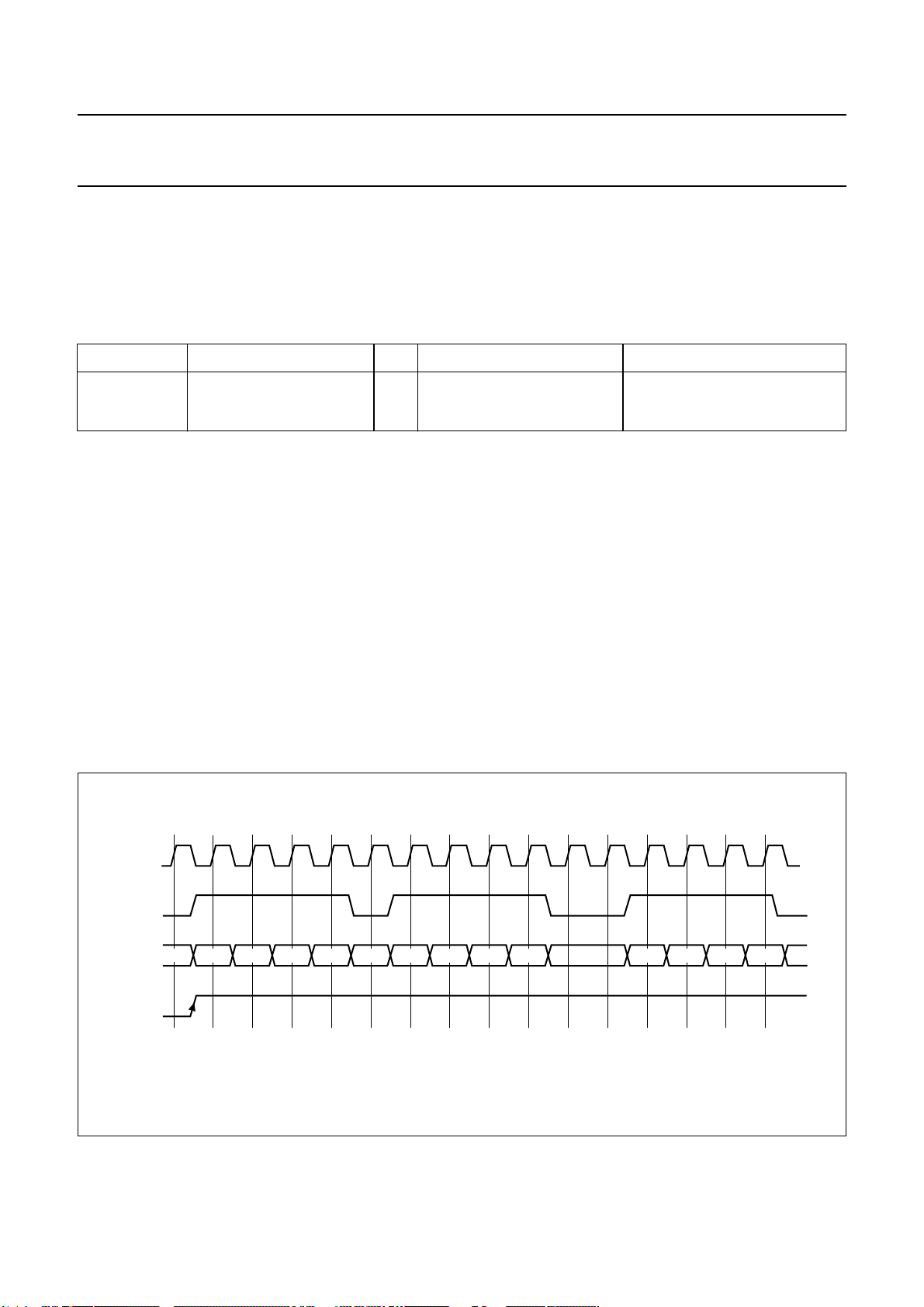
Philips Semiconductors Product specification
PAL/NTSC/SECAM video decoder with adaptive PAL/NTSC
SAA7114
comb filter, VBI data slicer and high performance scaler
9.6 Host port for 16-bit extension of video data I/O (H port)
The H port pins HPD can be used for extension of the data I/O paths to 16-bit.
The I port has functional priority. If I8_16[93H[6]] is set to logic 1 the output drivers of the H port are enabled depending
on the I port enable control. For I8_16 = 0, the HPD output is disabled.
Table 34 Signals dedicated to the host port
SYMBOL PIN
HPD7 to HPD0 A13, D12, C12, B12, A12,
C11, B11 and A11
(64 to 67 and 69 to 72)
Note
1. Pin numbers for LQFP100 in parenthesis.
9.7 Basic input and output timing diagrams I port
and X port
9.7.1 I PORT OUTPUT TIMING
The following diagrams illustrate the output timing via the
I port. IGPH and IGPV are logic 1 active gate signals.
If reference pulses are programmed, these pulses are
generated on the rising edge of the logic 1 active gates.
Valid data is accompanied by the output data qualifier on
pin IDQ. In addition invalid cycles are marked with output
code 00H.
The IDQ output pin may be defined to be a gated clock
output signal (ICLK AND internal IDQ).
(1)
I/O DESCRIPTION BIT
I/O 16-bit extension for digital I/O
(chrominance component)
IPE[1:0] 87H[1:0], ITRI[8FH[6]]
and I8_16[93H[6]]
9.7.2 X PORT INPUT TIMING
Atthe X port the input timing requirements arethesame as
those for the I port output. But different to those below:
• It is not necessary to mark invalid cycles with a 00H
code
• No constraints on the input qualifier (can be a random
pattern)
• XCLK may be a gated clock (XCLK AND external XDQ).
Remark: All timings illustrated in Figs 32 to 38 are given
for an uninterrupted output stream (no handshake with the
external hardware).
ICLK
IDQ
IPD[7:0
IGPH
]
00 FF 00 00 SAV 00
C
Y
B
Fig.32 Output timing I port for serial 8-bit data at start of a line (ICODE = 1).
2004 Mar 03 71
C
Y00
R
C
B
C
Y
R
Y00
MHB550
Page 72
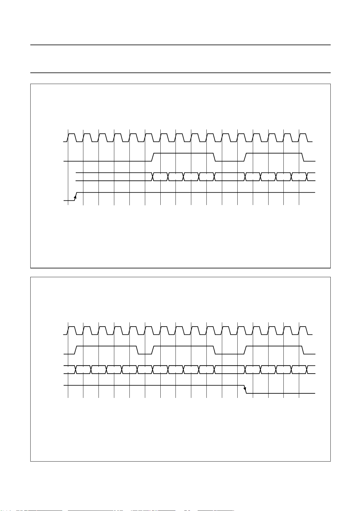
Philips Semiconductors Product specification
PAL/NTSC/SECAM video decoder with adaptive PAL/NTSC
comb filter, VBI data slicer and high performance scaler
ICLK
IDQ
IPD[7:0
IGPH
]
00
C
B
C
Y
Y00
R
C
B
SAA7114
C
Y
R
Y00
MHB551
ICLK
IDQ
IPD[7:0
IGPH
Fig.33 Output timing I port for serial 8-bit data at start of a line (ICODE = 0).
]
C
00
B
C
Y
R
Y00
C
B
C
Y
Y00FF0000EAV00
R
MHB552
Fig.34 Output timing I port for serial 8-bit data at end of a line (ICODE = 1).
2004 Mar 03 72
Page 73
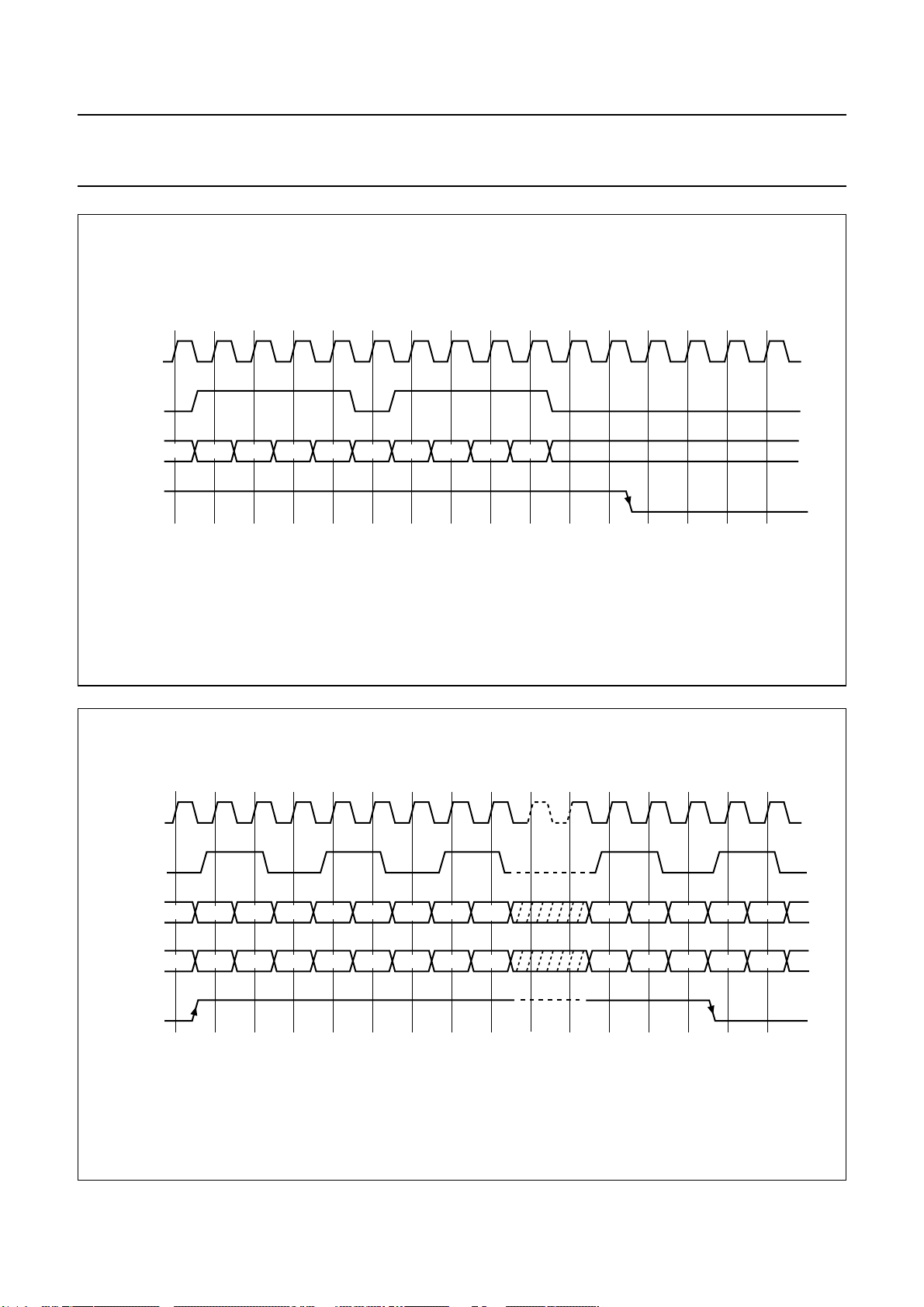
Philips Semiconductors Product specification
PAL/NTSC/SECAM video decoder with adaptive PAL/NTSC
comb filter, VBI data slicer and high performance scaler
ICLK
IDQ
IPD[7:0
IGPH
]
C
00
B
C
Y
R
Y00
C
B
C
Y
Y00
R
SAA7114
MHB553
ICLK
IDQ
IPD[7:0
HPD[7:0
IGPH
Fig.35 Output timing I port for serial 8-bit data at end of a line (ICODE = 0).
]
00 FF 00 00 Y0 Y1 00 Y2 Y3
]
00 00 SAV 00 00
C
C
B
R
C
B
Y
C
R
n−1
C
B
Y
00 FF 00 00
n
C
00 00 EAV 00
R
MHB554
Fig.36 Output timing for 16-bit data output via I port and H port with codes (ICODE = 1), timing is like 8-bit output,
but packages of 2 bytes per valid cycle.
2004 Mar 03 73
Page 74
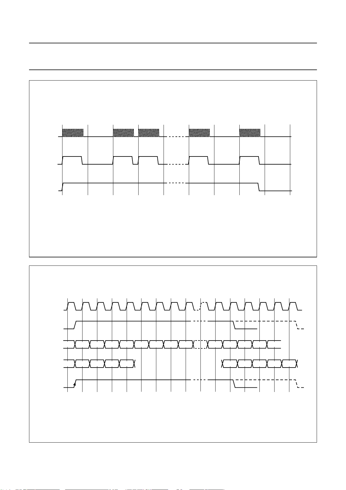
Philips Semiconductors Product specification
PAL/NTSC/SECAM video decoder with adaptive PAL/NTSC
comb filter, VBI data slicer and high performance scaler
handbook, full pagewidth
IDQ
IGPH
IGPV
SAA7114
MHB555
handbook, full pagewidth
ICLK
IDQ
]
IPD[7:0
]
HPD[7:0
sliced data
flag on IGP0
or IGP1
Fig.37 H gate and V gate output timing.
00 00 FF FF DID SDID XX YY ZZ CS
00 FF 00 SAV00 00 00BC FF EAV
BC
00 00 00
MHB733
Fig.38 Output timing for sliced VBI data in 8-bit serial output mode (dotted graphs for SAV/EAV mode).
2004 Mar 03 74
Page 75
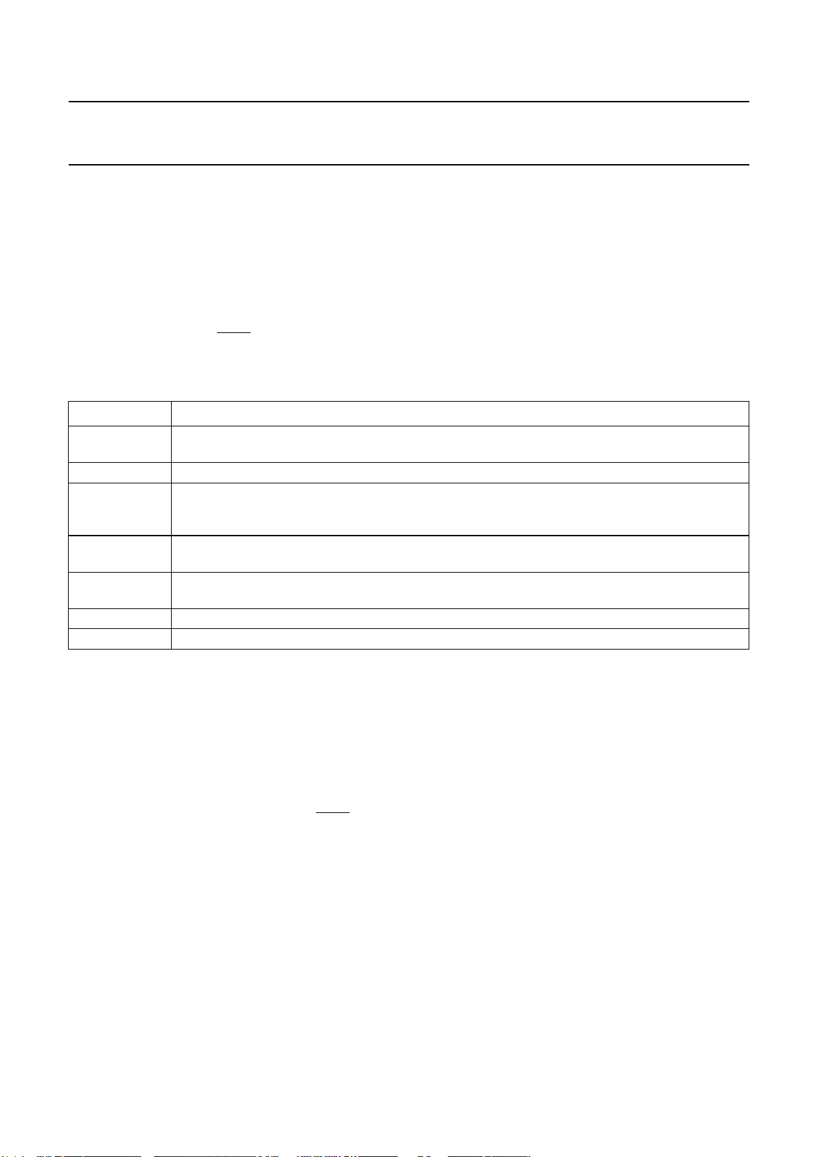
Philips Semiconductors Product specification
PAL/NTSC/SECAM video decoder with adaptive PAL/NTSC
SAA7114
comb filter, VBI data slicer and high performance scaler
10 BOUNDARY SCAN TEST
The SAA7114 has built-in logic and 5 dedicated pins to
support boundary scan testing which allows board testing
withoutspecial hardware (nails). The SAA7114 follows the
“IEEE Std. 1149.1 - Standard Test Access Port and
Boundary-Scan Architecture”
Group (JTAG) chaired by Philips.
The 5 special pins are Test Mode Select (TMS), Test
Clock (TCK), Test Reset (TRST), Test Data Input (TDI)
and Test Data Output (TDO).
Table 35 BST instructions supported by the SAA7114
INSTRUCTION DESCRIPTION
BYPASS This mandatory instruction provides a minimum length serial path (1 bit) between TDI and TDO
when no test operation of the component is required.
EXTEST This mandatory instruction allows testing of off-chip circuitry and board level interconnections.
SAMPLE This mandatory instruction can be used to take a sample of the inputs during normal operation of
the component. It can also be used to preload data values into the latched outputs of the boundary
scan register.
CLAMP This optional instruction is useful for testing when not all ICs have BST. This instruction addresses
the bypass register while the boundary scan register is in external test mode.
IDCODE This optional instruction will provide information on the components manufacturer,part number and
version number.
INTEST This optional instruction allows testing of the internal logic (no customer support available).
USER1 This private instruction allows testing by the manufacturer (no customer support available).
set by the Joint Test Action
The Boundary Scan Test (BST) functions BYPASS,
EXTEST, INTEST, SAMPLE, CLAMP and IDCODEare all
supported; see Table 35. Details about the JTAG
BST-TEST can be found in specification “
1149.1”
Description Language (BSDL) description of the SAA7114
is available on request.
. A file containing the detailed Boundary Scan
IEEE Std.
10.1 Initialization of boundary scan circuit
The Test Access Port (TAP) controller of an IC should be
in the reset state (TEST_LOGIC_RESET) when the IC is
in functional mode. This reset state also forces the
instruction register into a functional instruction such as
IDCODE or BYPASS.
To solve the power-up reset, the standard specifies that
the TAP controller will be forced asynchronously to the
TEST_LOGIC_RESET state by setting the TRST pin
LOW.
10.2 Device identification codes
A device identification register is specified in
1149.1b-1994”
for the specification of the IC manufacturer, the IC part
number and the IC version number. Its biggest advantage
is the possibility to check for the correct ICs mounted after
production and determination of the version number of ICs
during field service.
2004 Mar 03 75
. It is a 32-bit register which contains fields
“IEEE Std.
When the IDCODE instruction is loaded into the BST
instruction register, the identification register will be
connected between pins TDI and TDO of the IC. The
identification register will load a component specific code
duringthe CAPTURE_DATA_REGISTER state of theTAP
controller and this code can subsequently be shifted out.
At board level this code can be used to verify component
manufacturer, type and version number. The device
identification register contains 32 bits, numbered 31 to 0,
where bit D31 is the most significant bit (nearest to TDI)
and bit D0 is the least significant bit (nearest to TDO);
see Fig.39.
Page 76
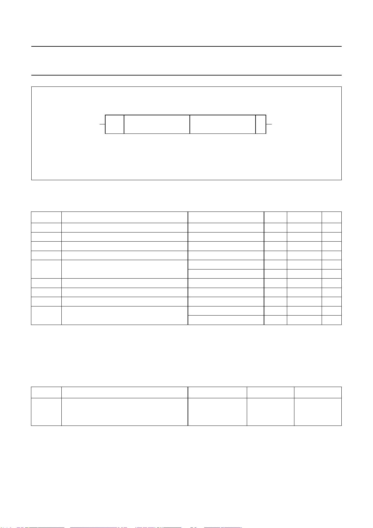
Philips Semiconductors Product specification
PAL/NTSC/SECAM video decoder with adaptive PAL/NTSC
SAA7114
comb filter, VBI data slicer and high performance scaler
MSB LSB
31
28 27 12 11 1 0
TDI TDO
nnnn
4-bit
version
code
000000101010111000100010100
16-bit part number 11-bit manufacturer
identification
Fig.39 32 bits of identification code.
11 LIMITING VALUES
In accordance with the Absolute Maximum Rating System (IEC 60134); all ground pins connected together and
grounded (0 V); all supply pins connected together.
SYMBOL PARAMETER CONDITIONS MIN. MAX. UNIT
V
V
V
V
V
DDD
DDA
i(A)
i(n)
i(D)
digital supply voltage −0.5 +4.6 V
analog supply voltage −0.5 +4.6 V
input voltage at analog inputs −0.5 +4.6 V
input voltage at pins XTALI, SDA and SCL −0.5 V
input voltage at digital inputs or I/O pins outputs in 3-state −0.5 +4.6 V
outputs in 3-state; note 1 −0.5 +5.5 V
∆V
T
T
V
SS
stg
amb
esd
voltage difference between V
SSA(n)
and V
SSD(n)
storage temperature −65 +150 °C
ambient temperature 0 70 °C
electrostatic discharge voltage human body model; note 2 −±2000 V
machine model; note 3 −±150 V
1
MHB557
+ 0.5 V
DDD
− 100 mV
Notes
1. Condition for maximum voltage at digital inputs or I/O pins: 3.0 V < V
DDD
< 3.6 V.
2. Class 2 according to EIA/JESD22-114-B.
3. Class A according to EIA/JESD22-115-A.
12 THERMAL CHARACTERISTICS
SYMBOL PARAMETER CONDITIONS VALUE UNIT
R
th(j-a)
thermal resistance from junction to ambient in free air
SAA7114E 38
SAA7114H 38
(1)
(1)
K/W
K/W
Note
1. The overall R
value can vary depending on the board layout. To minimize the effective R
th(j-a)
all power and
th(j-a)
ground pins must be connected to the power and ground layers directly. An ample copper area direct under the
SAA7114 with a number of through-hole plating, which connect to the ground layer (four-layer board: second layer),
can also reduce the effective R
. Please do not use any solder-stop varnish under the chip. In addition the usage
th(j-a)
of soldering glue with a high thermal conductance after curing is recommended.
2004 Mar 03 76
Page 77
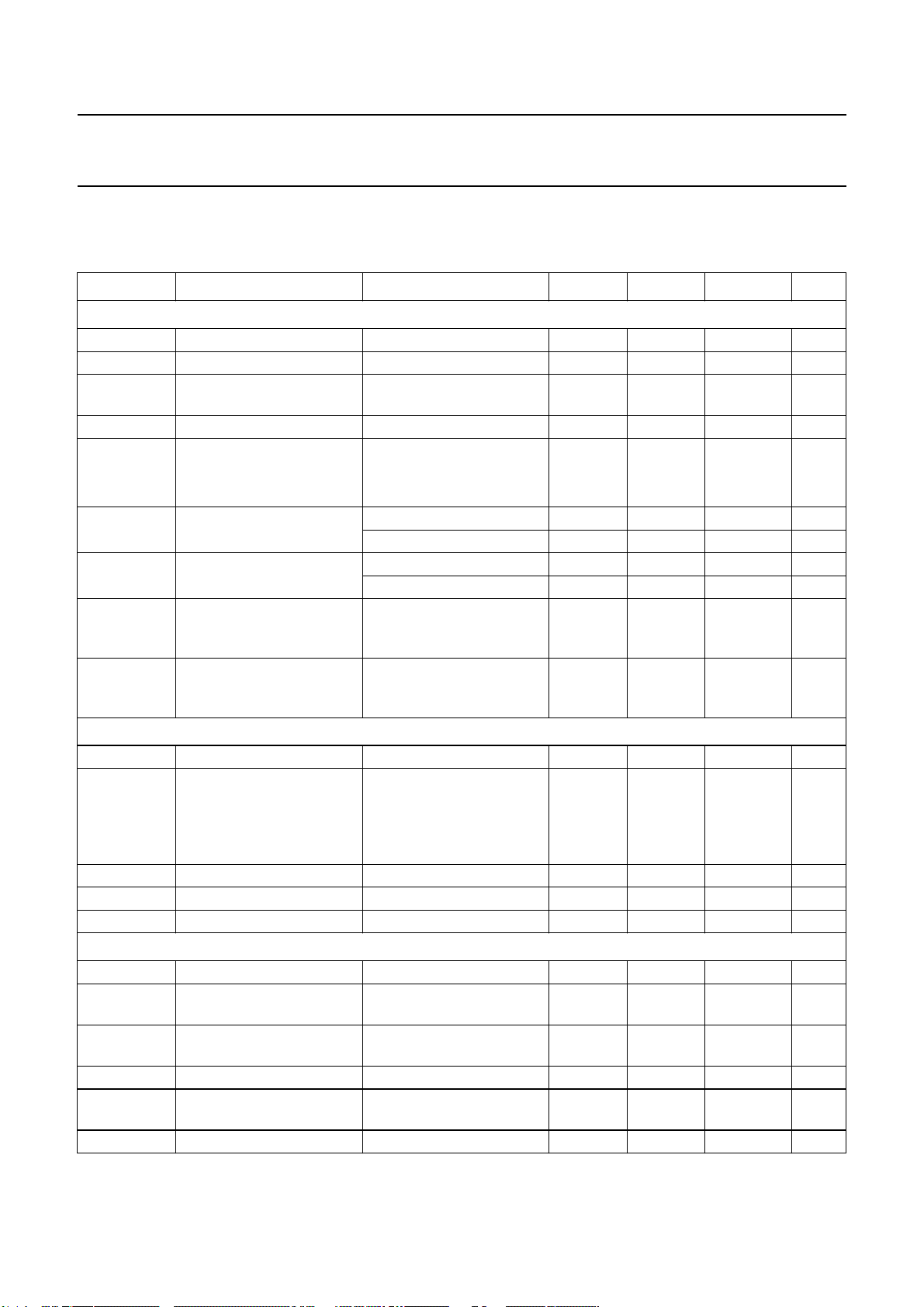
Philips Semiconductors Product specification
PAL/NTSC/SECAM video decoder with adaptive PAL/NTSC
SAA7114
comb filter, VBI data slicer and high performance scaler
13 CHARACTERISTICS
V
= 3.0 to 3.6 V; V
DDD
drawings and conditions illustrated in Fig.40; unless otherwise specified.
SYMBOL PARAMETER CONDITIONS MIN. TYP. MAX. UNIT
Supplies
V
I
DDD
P
DDD
D
digital supply voltage 3.0 3.3 3.6 V
digital supply current X port 3-state; 8-bit I port − 90 − mA
power dissipation digital
part
V
I
DDA
P
DDA
A
analog supply voltage 3.1 3.3 3.5 V
analog supply current AOSL1 and AOSL0 = 0
power dissipation analog
part
P
tot(A+D)
total power dissipation
analog and digital part
P
tot(A+D)(pd)
total power dissipation
analog and digital part in
power-down mode
P
tot(A+D)(ps)
total power dissipation
analog and digital part in
power-save mode
Analog part
I
clamp
V
i(p-p)
clamping current VI= 0.9 V DC −±8 −µA
input voltage
(peak-to-peak value)
Zi input impedance clamping current off 200 −− kΩ
C
i
α
cs
input capacitance −−10 pF
channel crosstalk fi< 5 MHz −−−50 dB
9-bit analog-to-digital converters
B analog bandwidth at −3dB − 7 − MHz
φ
diff
G
diff
f
clk(ADC)
LE
dc(d)
differential phase amplifier plus anti-alias
differential gain amplifier plus anti-alias
ADC clock frequency 12.8 − 14.3 MHz
DC differential linearity
error
LE
dc(i)
DC integral linearity error − 1 − LSB
= 3.1 to 3.5 V; T
DDA
= 0 to 70 °C (typical values excluded); timings and levels refer to
amb
− 300 − mW
CVBS mode − 47 − mA
Y/C mode − 72 − mA
CVBS mode − 150 − mW
Y/C mode − 240 − mW
CVBS mode − 450 − mW
Y/C mode − 540 − mW
CE pulled down to ground − 5 − mW
I2C-bus controlled via
− 75 − mW
subaddress 88H = 0FH
for normal video levels
− 0.7 − V
1 V (p-p), −3dB
termination 27/47 Ω and
AC coupling required;
coupling capacitor = 22 nF
− 2 − deg
filter bypassed
− 2 − %
filter bypassed
− 0.7 − LSB
2004 Mar 03 77
Page 78
Philips Semiconductors Product specification
PAL/NTSC/SECAM video decoder with adaptive PAL/NTSC
SAA7114
comb filter, VBI data slicer and high performance scaler
SYMBOL PARAMETER CONDITIONS MIN. TYP. MAX. UNIT
Digital inputs
V
IL(SCL,SDA)
V
IH(SCL,SDA)
V
IL(XTALI)
V
IH(XTALI)
V
IL(n)
V
IH(n)
I
LI
I
LI/O
C
i
Digital outputs; note 1
V
OL(SDA)
V
OL(clk)
V
OH(clk)
V
OL(n)
V
OH(n)
Clock output timing (LLC and LLC2); note 2
C
L
T
cy
δ duty factors for t
t
r
t
f
t
d(LLC-LLC2)
Horizontal PLL
f
hor(nom)
∆f
hor/fhor(nom)
LOW-level input voltage
−0.5 − +0.3V
DDD
V
pins SDA and SCL
HIGH-level input voltage
0.7V
DDD
− V
DDD
+ 0.5 V
pins SDA and SCL
LOW-level CMOS input
−0.3 − +0.8 V
voltage pin XTALI
HIGH-level CMOS input
2.0 − V
DDD
+ 0.3 V
voltage pin XTALI
LOW-level input voltage all
−0.3 − +0.8 V
other inputs
HIGH-levelinputvoltageall
2.0 − 5.5 V
other inputs
input leakage current −−1 µA
I/O leakage current −−10 µA
input capacitance I/O at high impedance −−8pF
LOW-level output voltage
SDA at 3 mA sink current −−0.4 V
pin SDA
LOW-level output voltage
−0.5 − +0.6 V
for clocks
HIGH-level output voltage
2.4 − V
DDD
+ 0.5 V
for clocks
LOW-level output voltage
0 − 0.4 V
all other digital outputs
HIGH-level output voltage
2.4 − V
DDD
+ 0.5 V
all other digital outputs
output load capacitance 15 − 50 pF
cycle time pin LLC 35 − 39 ns
pin LLC2 70 − 78 ns
LLCH/tLLC
and t
LLC2H/tLLC2
rise time LLC and LLC2 0.2 V to V
fall time LLC and LLC2 V
delay time between LLC
and LLC2 output
CL=40pF 40 − 60 %
− 0.2 V −−5ns
DDD
− 0.2 V to 0.2 V −−5ns
DDD
measured at 1.5 V;
−4 − +8 ns
CL=25pF
nominal line frequency 50 Hz field − 15625 − Hz
60 Hz field − 15734 − Hz
permissible static deviation −−5.7 %
2004 Mar 03 78
Page 79
Philips Semiconductors Product specification
PAL/NTSC/SECAM video decoder with adaptive PAL/NTSC
SAA7114
comb filter, VBI data slicer and high performance scaler
SYMBOL PARAMETER CONDITIONS MIN. TYP. MAX. UNIT
Subcarrier PLL
f
sc(nom)
∆f
sc
Crystal oscillator for 32.11 MHz; note 3
f
xtal(nom)
∆f
xtal(nom)
∆f
xtal(nom)(T)
CRYSTAL SPECIFICATION (X1)
T
amb(X1)
C
L
R
s
C
1
C
0
Crystal oscillator for 24.576 MHz; note 3
f
xtal(nom)
∆f
xtal(nom)
∆f
xtal(nom)(T)
CRYSTAL SPECIFICATION (X1)
T
amb(X1)
C
L
R
s
C
1
C
0
Clock input timing (XCLK)
T
cy
δ duty factors for t
t
r
t
f
Data and control signal input timing X port, related to XCLK input
t
SU;DAT
nominal subcarrier
frequency
PAL BGHI − 4433619 − Hz
NTSC M − 3579545 − Hz
PAL M − 3575612 − Hz
PAL N − 3582056 − Hz
lock-in range ±400 −− Hz
nominal frequency − 32.11 − MHz
permissible nominal
−−±70 × 10
−6
frequency deviation
permissible nominal
−−±30 × 10
−6
frequency deviation with
temperature
operating ambient
0 − 70 °C
temperature
load capacitance 8 −− pF
series resonance resistor − 40 80 Ω
motional capacitance − 1.5 ±20% − fF
parallel capacitance − 4.3 ±20% − pF
nominal frequency − 24.576 − MHz
permissible nominal
−−±50 × 10
−6
frequency deviation
permissible nominal
−−±20 × 10
−6
frequency deviation with
temperature
ambient temperature 0 − 70 °C
load capacitance 8 −− pF
series resonance resistor − 40 80 Ω
motional capacitance − 1.5 ±20% − fF
parallel capacitance − 3.5 ±20% − pF
cycle time 31 − 45 ns
LLCH/tLLC
40 50 60 %
rise time −−5ns
fall time −−5ns
input data set-up time − 10 − ns
2004 Mar 03 79
Page 80
Philips Semiconductors Product specification
PAL/NTSC/SECAM video decoder with adaptive PAL/NTSC
SAA7114
comb filter, VBI data slicer and high performance scaler
SYMBOL PARAMETER CONDITIONS MIN. TYP. MAX. UNIT
t
HD;DAT
Clock output timing
C
L
T
cy
δ duty factors for
t
r
t
f
Data and control signal output timing X port, related to XCLK output (for XPCK[1:0]83H[5:4] = 00 is default);
note 2
C
L
t
OHD;DAT
t
PD
Control signal output timing RT port, related to LLC output
C
L
t
OHD;DAT
t
PD
ICLK output timing
C
L
T
cy
δ duty factors for t
t
r
t
f
Data and control signal output timing I port, related to ICLK output (for IPCK[1:0]87H[5:4] = 00 is default)
C
L
t
OHD;DAT
t
o(d)
ICLK input timing
T
cy
Notes
1. The levels must be measured with load circuits; 1.2 kΩ at 3 V (TTL load); CL= 50 pF.
2. The effects of rise and fall times are included in the calculation of t
drawings and conditions illustrated in Fig.40.
3. The crystal oscillator drive level is typical 0.28 mW.
input data hold time − 3 − ns
output load capacitance 15 − 50 pF
cycle time 35 − 39 ns
35 − 65 %
t
XCLKH/tXCLKL
rise time 0.6 to 2.6 V −−5ns
fall time 2.6 to 0.6 V −−5ns
output load capacitance 15 − 50 pF
output data hold time CL=15pF − 14 − ns
propagation delay from
CL=15pF − 24 − ns
positive edge of XCLK
output
output load capacitance 15 − 50 pF
output hold time CL=15pF − 14 − ns
propagation delay from
CL=15pF − 24 − ns
positive edge of LLC
output
output load capacitance 15 − 50 pF
cycle time 31 − 45 ns
ICLKH/tICLKL
35 − 65 %
rise time 0.6 to 2.6 V −−5ns
fall time 2.6 to 0.6 V −−5ns
output load capacitance at
15 − 50 pF
all outputs
output data hold time CL=15pF − 12 − ns
output delay time CL=15pF − 22 − ns
cycle time 31 − 100 ns
OHD;DAT
and tPD. Timings and levels refer to
2004 Mar 03 80
Page 81
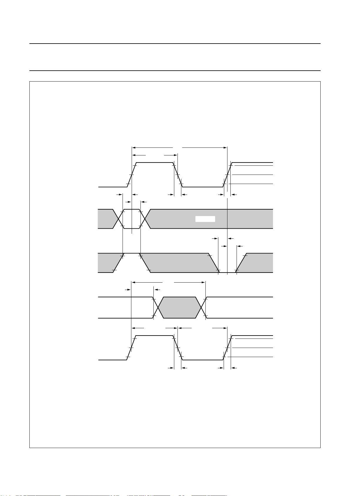
Philips Semiconductors Product specification
PAL/NTSC/SECAM video decoder with adaptive PAL/NTSC
comb filter, VBI data slicer and high performance scaler
handbook, full pagewidth
clock input
XCLK
data and
control inputs
(X port)
t
SU;DAT
t
XCLKH
t
HD;DAT
T
cy
t
f
not valid
t
r
SAA7114
2.4 V
1.5 V
0.6 V
2.0 V
0.8 V
input
XDQ
data and
control outputs
X port, I port
clock outputs
LLC, LLC2, XCLK, ICLK
and ICLK input
t
OHD;DAT
t
X(I)CLKH
t
o(d)
t
SU;DAT
t
HD;DAT
2.0 V
0.8 V
−2.4 V
−0.6 V
t
X(I)CLKL
−2.6 V
−1.5 V
−0.6 V
t
f
t
r
MHB735
Fig.40 Data input/output timing diagram (X port, RT port and I port).
2004 Mar 03 81
Page 82
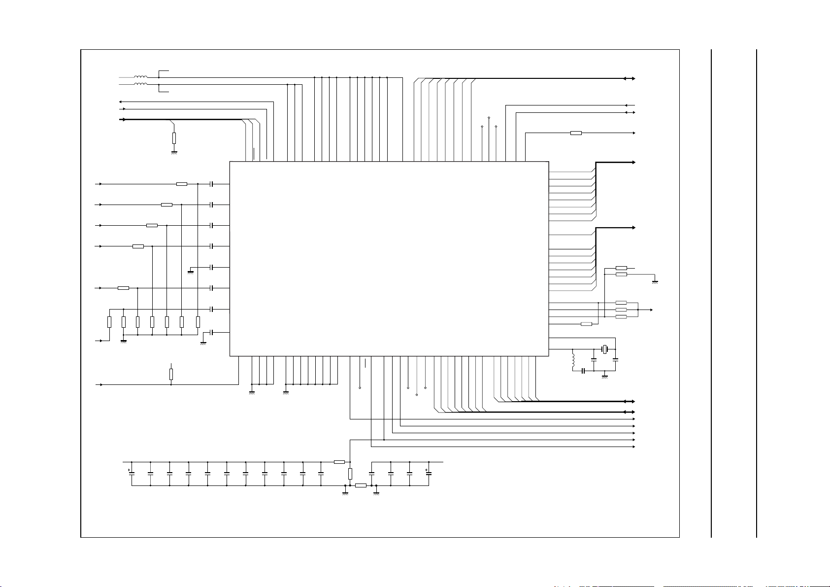
This text is here in white to force landscape pages to be rotated correctly when browsing through the pdf in the Acrobat reader.This text is here in
_white to force landscape pages to be rotated correctly when browsing through the pdf in the Acrobat reader.This text is here inThis text is here in
white to force landscape pages to be rotated correctly when browsing through the pdf in the Acrobat reader. white to force landscape pages to be ...
2004 Mar 03 82
V
DD(3.3)
V
DDA(3.3)
BST[2:0
AI24
AI23
AI22
AI21
AI12
R6
18
Ω
AI11
CE
3.3 V (D)
TDO
L2 2.2 µH
L3 2.2 µH
TDI
]
R4
18 Ω
R1
18 Ω
R7
R8
56
56
Ω
Ω
AGND
C24
10
µF
3.3 V (D)
3.3 V (A)
BST2
BST0
BST1
TCK
M6
(98)M5(99)N4(97)N6(3)N5(2)
P6 (10)
P7 (12)
P9 (14)
P10 (16)
P8 (13)
P11 (18)
P13 (20)
P12 (19)
(27)
N14
CE
AGND
C4
100
nF
(24)
N12
N13
V
TMS
SSA0
C5
100
nF
(15)
V
BST2
TRST
N8
N9
SSA1
DDA0VDDA1VDDA2VDDD(EP2)VDDD(EP4)
V
TDI
TDO
N11
(23)M9(17)M8(11)L9(25)
(9)
M7
(26)
(100)
(76)
(50)
(21)
N7
M13
L6
H4
H11
N10
SSA2
AGND
V
SSD(EP1)
SSD(EP2)
SSD(EP3)
V
V
V
V
DGND
Strapping
2
C-bus slave address
I
C6
C12
100
nF
C10
100
nF
DDD(EP1)VDDD(ICO1)VDDD(ICO2)VDDD(ICO3)VDDD(ICO4)VDDD(ICO5)VDDD(ICO6)
DDD(EP3)
V
V
D10
G11
L7
(1)
(51)
(75)
L11
(33)
(43)
J11
F11
(58)
D11
(68)J4(83)L4(93)
SAA7114E
(SAA7114H)
TP1
(29)
L14
LLC2
R16
0 Ω
(30)
M12
RES
C13
100
(36)
L13
RTCO
nF
(5)
(88)
P5
K4
SS(XTAL)
SSD(EP4)
V
V
100
nF
(63)
(38)
E11
K11
SSD(ICO3)
SSD(ICO2)
SSD(ICO1)
V
V
R19 open
C11
R23
100
3.3
nF
kΩ
DGND AGND
(28)
M14
LLC
Place 0 Ω
R24
if BST is not used
0 Ω
DGND
C17
R5
18 Ω
R3
18 Ω
R2
18 Ω
AGND
R9
R10
R11
Ω
3.3 V (D)
R14
R12
56
Ω
C7
100
nF
56
56
Ω
3.3 kΩ
C9
100
nF
AI24
47 nF
C14
AI23
47 nF
C15
AI22
47 nF
C16
AI21
47 nF
C25
AI2D
47 nF
C18
AI12
47 nF
C19
AI11
47 nF
56
C26
Ω
AI1D
47 nF
AGND
C2
C3
100
100
nF
nF
(35)
L10
RTS1
C8
100
(34)
K13
nF
V
L8
(8)
RTS0
HPD0
DD(XTAL)
HPD0
A11
(72)
(44)
(73)
H13
B10
TEST0
TP5
TP6
100
HPD1
B11
(71)
TEST1
C1
nF
HPD1
(74)
C10
TP7
HPD2
HPD2
C11
(70)
(81)
TEST2
K2
XPD7
XPD7
C23
10
µF
HPD3
A12
(69)
HPD3
(82)
K3
XPD6
XPD6
HPD4
HPD4
B12
(67)
(84)
L1
XPD5
XPD5
3.3 V (A)
C12
(66)
(85)
HPD5
HPD5
L2
XPD4
XPD4
(86)
D12
(65)
L3
HPD6
HPD6
XPD3
XPD3
HPD7
HPD7
A13
(64)J3(77)
(87)
(89)
M1
M2
XPD2
XPD2
TP3
TP4TP2
TEST3
SCL
SDA
TEST5
(91)
L5
XRV
XCON1
M11
(31)
(96)
N3
L12
(32)
(95)
M4
XDQ
XRDY
XCON2
XCON3
M10
(22)
(94)
M3
XCLK
XCON4
AOUT
(80)
K1
XTRI
XCON5
(54) E14
(55) D14
(56) C14
(57) B14
(59) E13
(60) D13
(61) C13
(62) B13
(42) J14
(45) H12
(46) H14
(47) G14
(48) F14
(49) G13
(52) F13
(53) G12
(37) K12
(39) K14
(40) J13
(41) J12
(6) P3
(4)
P4
XTOUT
XCON6
(7)
P2
IPD7
IPD6
IPD5
IPD4
IPD3
IPD2
IPD1
IPD0
ITRDY
ICLK
IDQ
ITRI
IGP0
IGP1
IGPV
IGPH
AMCLK
ASCLK
ALRCLK
AMXCLK
XTALO
XTALI
XPD1
XPD1
(90)
N1
XPD0
XPD0
TEST4
J1
(78)J2(79)
(92)
N2
XRH
XCON0
Pin numbers for LQFP in parenthesis.
10 µH
L1
R17
0 Ω
IMCON7
IMCON6
IMCON5
IMCON4
IMCON3
IMCON2
IMCON1
IMCON0
IPD7
IPD6
IPD5
IPD4
IPD3
IPD2
IPD1
IPD0
R20 open
24.576 MHz
C22
1 nF
Y1
C20
10 pF
DGND
R13 open
R15 3.3 kΩ
Strapping
clock frequency
R18 0 Ω
R21 open
R22 open
C21
10 pF
HPDL[7:0
SCL
SDA
AOUT
IPDL[7:0
IMCON[7:0
3.3 V (D)
DGND
XCON[7:0
XPD[7:0
LLC
RTS0
RTS1
RTCO
RESON
MHC614
]
]
ACLK
]
]
14 APPLICATION INFORMATION
comb filter, VBI data slicer and high performance scaler
]
Philips Semiconductors Product specification
PAL/NTSC/SECAM video decoder with adaptive PAL/NTSC
SAA7114
Fig.41 Application example with 24.576 MHz crystal.
handbook, full pagewidth
Page 83
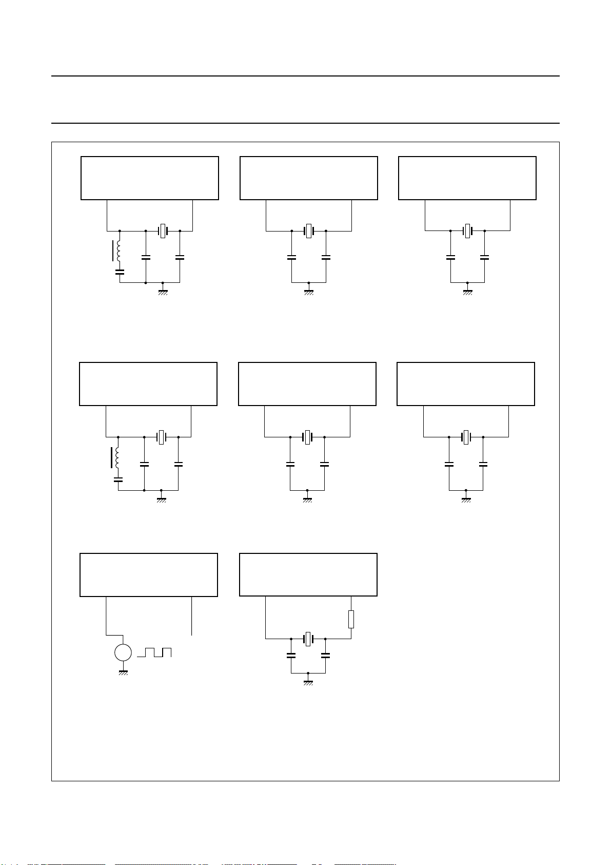
Philips Semiconductors Product specification
PAL/NTSC/SECAM video decoder with adaptive PAL/NTSC
comb filter, VBI data slicer and high performance scaler
handbook, full pagewidth
P2 (7)
XTALI XTALO
4.7 µH
1 nF
(1a) With 3rd harmonic quartz.
Crystal load = 8 pF.
handbook, full pagewidth
P2 (7)
XTALI XTALO
SAA7114
32.11 MHz
15
pF
SAA7114
24.576 MHz
P3 (6)
15
pF
P3 (6)
P2 (7)
(1b) With fundamental quartz.
Crystal load = 20 pF.
P2 (7)
SAA7114
P3 (6)
XTALI XTALO
32.11 MHz
33
pF
33
pF
SAA7114
P3 (6)
XTALI XTALO
24.576 MHz
P2 (7)
(1c) With fundamental quartz.
Crystal load = 8 pF
P2 (7)
SAA7114
SAA7114
P3 (6)
XTALI XTALO
32.11 MHz
10
pF
SAA7114
XTALI XTALO
24.576 MHz
10
pF
MHC615
P3 (6)
4.7 µH
1 nF
(2a) With 3rd harmonic quartz.
Crystal load = 8 pF.
18
pF
18
pF
SAA7114
P2 (7)
XTALI XTALO
32.11 MHz or
24.576 MHz
clock
(3a) With direct clock.
Pin numbers for LQFP100 in parenthesis.
P3 (6)
n.c.
39
pF
(2b) With fundamental quartz.
Crystal load = 20 pF.
pF
39
15
pF
(2c) With fundamental quartz.
Crystal load = 8 pF.
15
pF
MHC616
SAA7114
P2 (7)
XTALI XTALO
(3b) With fundamental quartz and restricted drive level. When P
is too high a resistance R
Note: The decreased crystal amplitude results in a lower drive level but on the other hand
the jitter performance will decrease.
P3 (6)
R
s
MHC617
of the internal oscillator
can be placed in series with the output of the oscillator XTALO.
s
drive
Fig.42 Oscillator application.
2004 Mar 03 83
Page 84
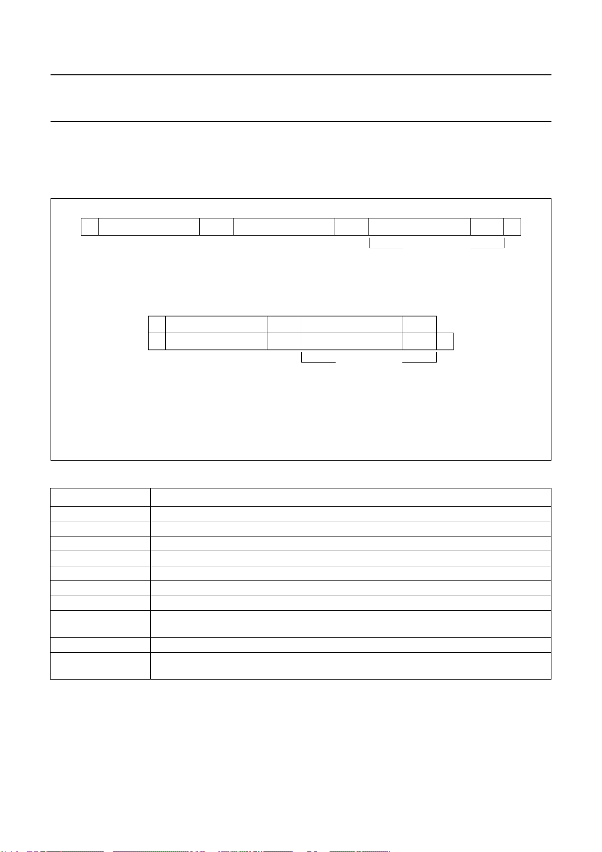
Philips Semiconductors Product specification
PAL/NTSC/SECAM video decoder with adaptive PAL/NTSC
comb filter, VBI data slicer and high performance scaler
15 I2C-BUS DESCRIPTION
The SAA7114 supports the ‘fast mode’ I2C-bus specification extension (data rate up to 400 kbits/s).
2
15.1 I
C-bus format
ACK-s ACK-s
SUBADDRESS
DATASLAVE ADDRESS W
data transferred
(n bytes + acknowledge)
a. Write procedure.
ACK-s ACK-s
ACK-s ACK-mSLAVE ADDRESS R
SUBADDRESSSLAVE ADDRESS WS
DATA
data transferred
(n bytes + acknowledge)
PSr
MHB340
SAA7114
PS ACK-s
MHB339
b. Read procedure (combined).
Fig.43 I2C-bus format.
Table 36 Description of I
2
C-bus format
CODE DESCRIPTION
S START condition
Sr repeated START condition
SLAVE ADDRESS W ‘0100 0010’ (42H, default) or ‘0100 0000’ (40H; note 1)
SLAVE ADDRESS R ‘0100 0011’ (43H, default) or ‘0100 0001’ (41H; note 1)
ACK-s acknowledge generated by the slave
ACK-m acknowledge generated by the master
SUBADDRESS subaddress byte; see Tables 37 and 38
DATA data byte; see Table 38; if more than one byte DATA is transmitted the subaddress pointer is
automatically incremented
P STOP condition
X read/write control bit (LSB slave address); X = 0, order to write (the circuit is slave receiver);
X = 1, order to read (the circuit is slave transmitter)
Note
1. If pin RTCO strapped to supply voltage via a 3.3 kΩ resistor.
2004 Mar 03 84
Page 85
Philips Semiconductors Product specification
PAL/NTSC/SECAM video decoder with adaptive PAL/NTSC
SAA7114
comb filter, VBI data slicer and high performance scaler
Table 37 Subaddress description and access
SUBADDRESS DESCRIPTION ACCESS (READ/WRITE)
00H chip version read only
F0H to FFH reserved −
Video decoder: 01H to 2FH
01H to 05H front-end part read and write
06H to 19H decoder part read and write
1AH to 1EH reserved −
1FH video decoder status byte read only
20H to 2FH reserved −
Audio clock generation: 30H to 3FH
30H to 3AH audio clock generator read and write
3BH to 3FH reserved −
General purpose VBI data slicer: 40H to 7FH
40H to 5EH VBI data slicer read and write
5FH reserved −
60H to 62H VBI data slicer status read only
63H to 7FH reserved −
X port, I port and the scaler: 80H to EFH
80H to 8FH task independent global settings read and write
90H to BFH task A definition read and write
C0H to EFH task B definition read and write
2004 Mar 03 85
Page 86
This text is here in white to force landscape pages to be rotated correctly when browsing through the pdf in the Acrobat reader.This text is here in
_white to force landscape pages to be rotated correctly when browsing through the pdf in the Acrobat reader.This text is here inThis text is here in
white to force landscape pages to be rotated correctly when browsing through the pdf in the Acrobat reader. white to force landscape pages to be ...
2004 Mar 03 86
Table 38 I
Chip version: register 00H
Chip version (read only) 00 ID7 ID6 ID5 ID4 −−−−
Video decoder: registers 01H to 2FH
FRONT-END PART: REGISTERS 01H TO 05H
Increment delay 01
Analog input control 1 02 FUSE1 FUSE0 GUDL1 GUDL0 MODE3 MODE2 MODE1 MODE0
Analog input control 2 03
Analog input control 3 04 GAI17 GAI16 GAI15 GAI14 GAI13 GAI12 GAI11 GAI10
Analog input control 4 05 GAI27 GAI26 GAI25 GAI24 GAI23 GAI22 GAI21 GAI20
DECODER PART: REGISTERS 06H TO 2FH
Horizontal sync start 06 HSB7 HSB6 HSB5 HSB4 HSB3 HSB2 HSB1 HSB0
Horizontal sync stop 07 HSS7 HSS6 HSS5 HSS4 HSS3 HSS2 HSS1 HSS0
Sync control 08 AUFD FSEL FOET HTC1 HTC0 HPLL VNOI1 VNOI0
Luminance control 09 BYPS YCOMB LDEL LUBW LUFI3 LUFI2 LUFI1 LUFI0
Luminance brightness control 0A DBRI7 DBRI6 DBRI5 DBRI4 DBRI3 DBRI2 DBRI1 DBRI0
Luminance contrast control 0B DCON7 DCON6 DCON5 DCON4 DCON3 DCON2 DCON1 DCON0
Chrominance saturation control 0C DSAT7 DSAT6 DSAT5 DSAT4 DSAT3 DSAT2 DSAT1 DSAT0
Chrominance hue control 0D HUEC7 HUEC6 HUEC5 HUEC4 HUEC3 HUEC2 HUEC1 HUEC0
Chrominance control 1 0E CDTO CSTD2 CSTD1 CSTD0 DCVF FCTC
Chrominance gain control 0F ACGC CGAIN6 CGAIN5 CGAIN4 CGAIN3 CGAIN2 CGAIN1 CGAIN0
Chrominance control 2 10 OFFU1 OFFU0 OFFV1 OFFV0 CHBW LCBW2 LCBW1 LCBW0
Mode/delay control 11 COLO RTP1 HDEL1 HDEL0 RTP0 YDEL2 YDEL1 YDEL0
RT signal control 12 RTSE13 RTSE12 RTSE11 RTSE10 RTSE03 RTSE02 RTSE01 RTSE00
RT/X port output control 13 RTCE XRHS XRVS1 XRVS0 HLSEL OFTS2 OFTS1 OFTS0
Analog/ADC/compatibility
control
VGATE start, FID change 15 VSTA7 VSTA6 VSTA5 VSTA4 VSTA3 VSTA2 VSTA1 VSTA0
VGATE stop 16 VSTO7 VSTO6 VSTO5 VSTO4 VSTO3 VSTO2 VSTO1 VSTO0
2
C-bus receiver/transmitter overview
REGISTER FUNCTION
SUB
ADDR.
(HEX)
14 CM99 UPTCV AOSL1 AOSL0 XTOUTE OLDSB APCK1 APCK0
D7 D6 D5 D4 D3 D2 D1 D0
(1) (1) (1) (1)
(1)
HLNRS VBSL WPOFF HOLDG GAFIX GAI28 GAI18
IDEL3 IDEL2 IDEL1 IDEL0
(1)
CCOMB
Philips Semiconductors Product specification
PAL/NTSC/SECAM video decoder with adaptive PAL/NTSC
comb filter, VBI data slicer and high performance scaler
SAA7114
Page 87
This text is here in white to force landscape pages to be rotated correctly when browsing through the pdf in the Acrobat reader.This text is here in
_white to force landscape pages to be rotated correctly when browsing through the pdf in the Acrobat reader.This text is here inThis text is here in
white to force landscape pages to be rotated correctly when browsing through the pdf in the Acrobat reader. white to force landscape pages to be ...
2004 Mar 03 87
SUB
REGISTER FUNCTION
ADDR.
D7 D6 D5 D4 D3 D2 D1 D0
(HEX)
Miscellaneous,
17 LLCE LLC2E
(1) (1) (1)
VGPS VSTO8 VSTA8
VGATE configuration and MSBs
Raw data gain control 18 RAWG7 RAWG6 RAWG5 RAWG4 RAWG3 RAWG2 RAWG1 RAWG0
Raw data offset control 19 RAWO7 RAWO6 RAWO5 RAWO4 RAWO3 RAWO2 RAWO1 RAWO0
Reserved 1A to 1E
Status byte video decoder
1F INTL HLVLN FIDT GLIMT GLIMB WIPA COPRO RDCAP
(1) (1) (1) (1) (1) (1) (1) (1)
(read only, OLDSB = 0)
Status byte video decoder
1F INTL HLCK FIDT GLIMT GLIMB WIPA SLTCA CODE
(read only, OLDSB = 1)
Reserved 20 to 2F
(1) (1) (1) (1) (1) (1) (1) (1)
Audio clock generator part: registers 30H to 3FH
Audio master clock cycles per
field
Reserved 33
Audio master clock nominal
increment
Reserved 37
Clock ratio AMXCLK to ASCLK 38
Clock ratio ASCLK to ALRCLK 39
Audio clock generator basic
30 ACPF7 ACPF6 ACPF5 ACPF4 ACPF3 ACPF2 ACPF1 ACPF0
31 ACPF15 ACPF14 ACPF13 ACPF12 ACPF11 ACPF10 ACPF9 ACPF8
32
(1) (1) (1) (1) (1) (1)
(1) (1) (1) (1) (1) (1) (1) (1)
ACPF17 ACPF16
34 ACNI7 ACNI6 ACNI5 ACNI4 ACNI3 ACNI2 ACNI1 ACNI0
35 ACNI15 ACNI14 ACNI13 ACNI12 ACNI11 ACNI10 ACNI9 ACNI8
36
3A
(1) (1)
(1) (1) (1) (1) (1) (1) (1) (1)
(1) (1)
(1) (1)
(1) (1) (1) (1)
ACNI21 ACNI20 ACNI19 ACNI18 ACNI17 ACNI16
SDIV5 SDIV4 SDIV3 SDIV2 SDIV1 SDIV0
LRDIV5 LRDIV4 LRDIV3 LRDIV2 LRDIV1 LRDIV0
APLL AMVR LRPH SCPH
set-up
Reserved 3B to 3F
(1) (1) (1) (1) (1) (1) (1) (1)
General purpose VBI data slicer part: registers 40H to 7FH
Slicer control 1 40
(1)
HAM_N FCE HUNT_N
(1) (1) (1) (1)
LCR2 to LCR24 (n = 2 to 24) 41 to 57 LCRn_7 LCRn_6 LCRn_5 LCRn_4 LCRn_3 LCRn_2 LCRn_1 LCRn_0
Programmable framing code 58 FC7 FC6 FC5 FC4 FC3 FC2 FC1 FC0
Horizontal offset for slicer 59 HOFF7 HOFF6 HOFF5 HOFF4 HOFF3 HOFF2 HOFF1 HOFF0
Vertical offset for slicer 5A VOFF7 VOFF6 VOFF5 VOFF4 VOFF3 VOFF2 VOFF1 VOFF0
Philips Semiconductors Product specification
PAL/NTSC/SECAM video decoder with adaptive PAL/NTSC
comb filter, VBI data slicer and high performance scaler
SAA7114
Page 88
This text is here in white to force landscape pages to be rotated correctly when browsing through the pdf in the Acrobat reader.This text is here in
_white to force landscape pages to be rotated correctly when browsing through the pdf in the Acrobat reader.This text is here inThis text is here in
white to force landscape pages to be rotated correctly when browsing through the pdf in the Acrobat reader. white to force landscape pages to be ...
2004 Mar 03 88
SUB
REGISTER FUNCTION
ADDR.
D7 D6 D5 D4 D3 D2 D1 D0
(HEX)
Field offset and MSBs for
5B FOFF RECODE
(1)
VOFF8
(1)
HOFF10 HOFF9 HOFF8
horizontal and vertical offset
Reserved (for testing) 5C
Header and data identification
5D FVREF
(1) (1) (1) (1) (1) (1) (1) (1)
(1)
DID5 DID4 DID3 DID2 DID1 DID0
(DID) code control
Sliced data identification (SDID)
5E
(1) (1)
SDID5 SDID4 SDID3 SDID2 SDID1 SDID0
code
Reserved 5F
(1) (1) (1) (1) (1) (1) (1) (1)
Slicer status byte 0 (read only) 60 − FC8V FC7V VPSV PPV CCV −−
Slicer status byte 1 (read only) 61 −−F21_N LN8 LN7 LN6 LN5 LN4
Slicer status byte 2 (read only) 62 LN3 LN2 LN1 LN0 DT3 DT2 DT1 DT0
Reserved 63 to 7F
(1) (1) (1) (1) (1) (1) (1) (1)
X port, I port and the scaler part: registers 80H to EFH
TASK INDEPENDENT GLOBAL SETTINGS: 80H TO 8FH
Global control 1 80
Reserved 81 and
(1)
(1) (1) (1) (1) (1) (1) (1) (1)
SMOD TEB TEA ICKS3 ICKS2 ICKS1 ICKS0
82
X port I/O enable and output
83
(1) (1)
XPCK1 XPCK0
(1)
XRQT XPE1 XPE0
clock phase control
I port signal definitions 84 IDG01 IDG00 IDG11 IDG10 IDV1 IDV0 IDH1 IDH0
I port signal polarities 85 ISWP1 ISWP0 ILLV IG0P IG1P IRVP IRHP IDQP
I port FIFO flag control and
86 VITX1 VITX0 IDG02 IDG12 FFL1 FFL0 FEL1 FEL0
arbitration
I port I/O enable, output clock
87 IPCK3 IPCK2 IPCK1 IPCK0
(1) (1)
IPE1 IPE0
and gated clock phase control
Power save control 88 CH4EN CH2EN SWRST DPROG SLM3
Reserved 89 to 8E
(1) (1) (1) (1) (1) (1) (1) (1)
(1)
SLM1 SLM0
Status information scaler part 8F XTRI ITRI FFIL FFOV PRDON ERROF FIDSCI FIDSCO
Philips Semiconductors Product specification
PAL/NTSC/SECAM video decoder with adaptive PAL/NTSC
comb filter, VBI data slicer and high performance scaler
SAA7114
Page 89
This text is here in white to force landscape pages to be rotated correctly when browsing through the pdf in the Acrobat reader.This text is here in
_white to force landscape pages to be rotated correctly when browsing through the pdf in the Acrobat reader.This text is here inThis text is here in
white to force landscape pages to be rotated correctly when browsing through the pdf in the Acrobat reader. white to force landscape pages to be ...
2004 Mar 03 89
SUB
REGISTER FUNCTION
ADDR.
D7 D6 D5 D4 D3 D2 D1 D0
(HEX)
TASK A DEFINITION: REGISTERS 90H TO BFH
Basic settings and acquisition window definition
Task handling control 90 CONLH OFIDC FSKP2 FSKP1 FSKP0 RPTSK STRC1 STRC0
X port formats and configuration 91 CONLV HLDFV SCSRC1 SCSRC0 SCRQE FSC2 FSC1 FSC0
X port input reference signal
92 XFDV XFDH XDV1 XDV0 XCODE XDH XDQ XCKS
definitions
I port output formats and
93 ICODE I8_16 FYSK FOI1 FOI0 FSI2 FSI1 FSI0
configuration
Horizontal input window start 94 XO7 XO6 XO5 XO4 XO3 XO2 XO1 XO0
95
(1) (1) (1) (1)
XO11 XO10 XO9 XO8
Horizontal input window length 96 XS7 XS6 XS5 XS4 XS3 XS2 XS1 XS0
97
(1) (1) (1) (1)
XS11 XS10 XS9 XS8
Vertical input window start 98 YO7 YO6 YO5 YO4 YO3 YO2 YO1 YO0
99
(1) (1) (1) (1)
YO11 YO10 YO9 YO8
Vertical input window length 9A YS7 YS6 YS5 YS4 YS3 YS2 YS1 YS0
9B
(1) (1) (1) (1)
YS11 YS10 YS9 YS8
Horizontal output window length 9C XD7 XD6 XD5 XD4 XD3 XD2 XD1 XD0
9D
(1) (1) (1) (1)
XD11 XD10 XD9 XD8
Vertical output window length 9E YD7 YD6 YD5 YD4 YD3 YD2 YD1 YD0
9F
(1) (1) (1) (1)
YD11 YD10 YD9 YD8
FIR filtering and prescaling
Horizontal prescaling A0
Accumulation length A1
Prescaler DC gain and FIR
A2 PFUV1 PFUV0 PFY1 PFY0 XC2_1 XDCG2 XDCG1 XDCG0
(1) (1)
(1) (1)
XPSC5 XPSC4 XPSC3 XPSC2 XPSC1 XPSC0
XACL5 XACL4 XACL3 XACL2 XACL1 XACL0
prefilter control
Reserved A3
(1) (1) (1) (1) (1) (1) (1) (1)
Luminance brightness control A4 BRIG7 BRIG6 BRIG5 BRIG4 BRIG3 BRIG2 BRIG1 BRIG0
Luminance contrast control A5 CONT7 CONT6 CONT5 CONT4 CONT3 CONT2 CONT1 CONT0
Chrominance saturation control A6 SATN7 SATN6 SATN5 SATN4 SATN3 SATN2 SATN1 SATN0
Reserved A7
(1) (1) (1) (1) (1) (1) (1) (1)
Philips Semiconductors Product specification
PAL/NTSC/SECAM video decoder with adaptive PAL/NTSC
comb filter, VBI data slicer and high performance scaler
SAA7114
Page 90
This text is here in white to force landscape pages to be rotated correctly when browsing through the pdf in the Acrobat reader.This text is here in
_white to force landscape pages to be rotated correctly when browsing through the pdf in the Acrobat reader.This text is here inThis text is here in
white to force landscape pages to be rotated correctly when browsing through the pdf in the Acrobat reader. white to force landscape pages to be ...
2004 Mar 03 90
SUB
REGISTER FUNCTION
ADDR.
D7 D6 D5 D4 D3 D2 D1 D0
(HEX)
Horizontal phase scaling
Horizontal luminance scaling
increment
Horizontal luminance phase
A8 XSCY7 XSCY6 XSCY5 XSCY4 XSCY3 XSCY2 XSCY1 XSCY0
A9
(1) (1) (1)
XSCY12 XSCY11 XSCY10 XSCY9 XSCY8
AA XPHY7 XPHY6 XPHY5 XPHY4 XPHY3 XPHY2 XPHY1 XPHY0
offset
Reserved AB
Horizontal chrominance scaling
increment
Horizontal chrominance phase
AC XSCC7 XSCC6 XSCC5 XSCC4 XSCC3 XSCC2 XSCC1 XSCC0
AD
AE XPHC7 XPHC6 XPHC5 XPHC4 XPHC3 XPHC2 XPHC1 XPHC0
(1) (1) (1) (1) (1) (1) (1) (1)
(1) (1) (1)
XSCC12 XSCC11 XSCC10 XSCC9 XSCC8
offset
Reserved AF
(1) (1) (1) (1) (1) (1) (1) (1)
Vertical scaling
Vertical luminance scaling
increment
Vertical chrominance scaling
increment
Vertical scaling mode control B4
Reserved B5 to B7
Vertical chrominance phase
B0 YSCY7 YSCY6 YSCY5 YSCY4 YSCY3 YSCY2 YSCY1 YSCY0
B1 YSCY15 YSCY14 YSCY13 YSCY12 YSCY11 YSCY10 YSCY9 YSCY8
B2 YSCC7 YSCC6 YSCC5 YSCC4 YSCC3 YSCC2 YSCC1 YSCC0
B3 YSCC15 YSCC14 YSCC13 YSCC12 YSCC11 YSCC10 YSCC9 YSCC8
(1) (1) (1)
(1) (1) (1) (1) (1) (1) (1) (1)
YMIR
(1) (1) (1)
B8 YPC07 YPC06 YPC05 YPC04 YPC03 YPC02 YPC01 YPC00
offset ‘00’
Vertical chrominance phase
B9 YPC17 YPC16 YPC15 YPC14 YPC13 YPC12 YPC11 YPC10
offset ‘01’
Vertical chrominance phase
BA YPC27 YPC26 YPC25 YPC24 YPC23 YPC22 YPC21 YPC20
offset ‘10’
Vertical chrominance phase
BB YPC37 YPC36 YPC35 YPC34 YPC33 YPC32 YPC31 YPC30
offset ‘11’
Vertical luminance phase
BC YPY07 YPY06 YPY05 YPY04 YPY03 YPY02 YPY01 YPY00
offset ‘00’
Vertical luminance phase
BD YPY17 YPY16 YPY15 YPY14 YPY13 YPY12 YPY11 YPY10
offset ‘01’
Vertical luminance phase
BE YPY27 YPY26 YPY25 YPY24 YPY23 YPY22 YPY21 YPY20
offset ‘10’
YMODE
Philips Semiconductors Product specification
PAL/NTSC/SECAM video decoder with adaptive PAL/NTSC
comb filter, VBI data slicer and high performance scaler
SAA7114
Page 91
This text is here in white to force landscape pages to be rotated correctly when browsing through the pdf in the Acrobat reader.This text is here in
_white to force landscape pages to be rotated correctly when browsing through the pdf in the Acrobat reader.This text is here inThis text is here in
white to force landscape pages to be rotated correctly when browsing through the pdf in the Acrobat reader. white to force landscape pages to be ...
2004 Mar 03 91
SUB
REGISTER FUNCTION
ADDR.
D7 D6 D5 D4 D3 D2 D1 D0
(HEX)
Vertical luminance phase
BF YPY37 YPY36 YPY35 YPY34 YPY33 YPY32 YPY31 YPY30
offset ‘11’
TASK B DEFINITION REGISTERS C0H TO EFH
Basic settings and acquisition window definition
Task handling control C0 CONLH OFIDC FSKP2 FSKP1 FSKP0 RPTSK STRC1 STRC0
X port formats and configuration C1 CONLV HLDFV SCSRC1 SCSRC0 SCRQE FSC2 FSC1 FSC0
Input reference signal definition C2 XFDV XFDH XDV1 XDV0 XCODE XDH XDQ XCKS
I port formats and configuration C3 ICODE I8_16 FYSK FOI1 FOI0 FSI2 FSI1 FSI0
Horizontal input window start C4 XO7 XO6 XO5 XO4 XO3 XO2 XO1 XO0
C5
(1) (1) (1) (1)
XO11 XO10 XO9 XO8
Horizontal input window length C6 XS7 XS6 XS5 XS4 XS3 XS2 XS1 XS0
C7
(1) (1) (1) (1)
XS11 XS10 XS9 XS8
Vertical input window start C8 YO7 YO6 YO5 YO4 YO3 YO2 YO1 YO0
C9
(1) (1) (1) (1)
YO11 YO10 YO9 YO8
Vertical input window length CA YS7 YS6 YS5 YS4 YS3 YS2 YS1 YS0
CB
(1) (1) (1) (1)
YS11 YS10 YS9 YS8
Horizontal output window length CC XD7 XD6 XD5 XD4 XD3 XD2 XD1 XD0
CD
(1) (1) (1) (1)
XD11 XD10 XD9 XD8
Vertical output window length CE YD7 YD6 YD5 YD4 YD3 YD2 YD1 YD0
CF
(1) (1) (1) (1)
YD11 YD10 YD9 YD8
FIR filtering and prescaling
Horizontal prescaling D0
Accumulation length D1
Prescaler DC gain and FIR
D2 PFUV1 PFUV0 PFY1 PFY0 XC2_1 XDCG2 XDCG1 XDCG0
(1) (1)
(1) (1)
XPSC5 XPSC4 XPSC3 XPSC2 XPSC1 XPSC0
XACL5 XACL4 XACL3 XACL2 XACL1 XACL0
prefilter control
Reserved D3
(1) (1) (1) (1) (1) (1) (1) (1)
Luminance brightness control D4 BRIG7 BRIG6 BRIG5 BRIG4 BRIG3 BRIG2 BRIG1 BRIG0
Luminance contrast control D5 CONT7 CONT6 CONT5 CONT4 CONT3 CONT2 CONT1 CONT0
Chrominance saturation control D6 SATN7 SATN6 SATN5 SATN4 SATN3 SATN2 SATN1 SATN0
Reserved D7
(1) (1) (1) (1) (1) (1) (1) (1)
Philips Semiconductors Product specification
PAL/NTSC/SECAM video decoder with adaptive PAL/NTSC
comb filter, VBI data slicer and high performance scaler
SAA7114
Page 92
This text is here in white to force landscape pages to be rotated correctly when browsing through the pdf in the Acrobat reader.This text is here in
_white to force landscape pages to be rotated correctly when browsing through the pdf in the Acrobat reader.This text is here inThis text is here in
white to force landscape pages to be rotated correctly when browsing through the pdf in the Acrobat reader. white to force landscape pages to be ...
2004 Mar 03 92
SUB
REGISTER FUNCTION
ADDR.
D7 D6 D5 D4 D3 D2 D1 D0
(HEX)
Horizontal phase scaling
Horizontal luminance scaling
increment
Horizontal luminance phase
D8 XSCY7 XSCY6 XSCY5 XSCY4 XSCY3 XSCY2 XSCY1 XSCY0
D9
(1) (1) (1)
XSCY12 XSCY11 XSCY10 XSCY9 XSCY8
DA XPHY7 XPHY6 XPHY5 XPHY4 XPHY3 XPHY2 XPHY1 XPHY0
offset
Reserved DB
Horizontal chrominance scaling
increment
Horizontal chrominance phase
DC XSCC7 XSCC6 XSCC5 XSCC4 XSCC3 XSCC2 XSCC1 XSCC0
DD
DE XPHC7 XPHC6 XPHC5 XPHC4 XPHC3 XPHC2 XPHC1 XPHC0
(1) (1) (1) (1) (1) (1) (1) (1)
(1) (1) (1)
XSCC12 XSCC11 XSCC10 XSCC9 XSCC8
offset
Reserved DF
(1) (1) (1) (1) (1) (1) (1) (1)
Vertical scaling
Vertical luminance scaling
increment
Vertical chrominance scaling
increment
Vertical scaling mode control E4
Reserved E5 to E7
Vertical chrominance phase
E0 YSCY7 YSCY6 YSCY5 YSCY4 YSCY3 YSCY2 YSCY1 YSCY0
E1 YSCY15 YSCY14 YSCY13 YSCY12 YSCY11 YSCY10 YSCY9 YSCY8
E2 YSCC7 YSCC6 YSCC5 YSCC4 YSCC3 YSCC2 YSCC1 YSCC0
E3 YSCC15 YSCC14 YSCC13 YSCC12 YSCC11 YSCC10 YSCC9 YSCC8
(1) (1) (1)
(1) (1) (1) (1) (1) (1) (1) (1)
YMIR
(1) (1) (1)
E8 YPC07 YPC06 YPC05 YPC04 YPC03 YPC02 YPC01 YPC00
offset ‘00’
Vertical chrominance phase
E9 YPC17 YPC16 YPC15 YPC14 YPC13 YPC12 YPC11 YPC10
offset ‘01’
Vertical chrominance phase
EA YPC27 YPC26 YPC25 YPC24 YPC23 YPC22 YPC21 YPC20
offset ‘10’
Vertical chrominance phase
EB YPC37 YPC36 YPC35 YPC34 YPC33 YPC32 YPC31 YPC30
offset ‘11’
Vertical luminance phase
EC YPY07 YPY06 YPY05 YPY04 YPY03 YPY02 YPY01 YPY00
offset ‘00’
YMODE
Philips Semiconductors Product specification
PAL/NTSC/SECAM video decoder with adaptive PAL/NTSC
comb filter, VBI data slicer and high performance scaler
SAA7114
Page 93
This text is here in white to force landscape pages to be rotated correctly when browsing through the pdf in the Acrobat reader.This text is here in
_white to force landscape pages to be rotated correctly when browsing through the pdf in the Acrobat reader.This text is here inThis text is here in
white to force landscape pages to be rotated correctly when browsing through the pdf in the Acrobat reader. white to force landscape pages to be ...
2004 Mar 03 93
SUB
REGISTER FUNCTION
Vertical luminance phase
offset ‘01’
Vertical luminance phase
offset ‘10’
Vertical luminance phase
offset ‘11’
Note
1. All unused control bits must be programmed with logic 0 to ensure compatibility to future enhancements.
ADDR.
(HEX)
ED YPY17 YPY16 YPY15 YPY14 YPY13 YPY12 YPY11 YPY10
EE YPY27 YPY26 YPY25 YPY24 YPY23 YPY22 YPY21 YPY20
EF YPY37 YPY36 YPY35 YPY34 YPY33 YPY32 YPY31 YPY30
D7 D6 D5 D4 D3 D2 D1 D0
Philips Semiconductors Product specification
PAL/NTSC/SECAM video decoder with adaptive PAL/NTSC
comb filter, VBI data slicer and high performance scaler
SAA7114
Page 94
Philips Semiconductors Product specification
PAL/NTSC/SECAM video decoder with adaptive PAL/NTSC
SAA7114
comb filter, VBI data slicer and high performance scaler
15.2 I2C-bus details
15.2.1 SUBADDRESS 00H
Table 39 Chip Version (CV) identification; 00H[7:4]; read only register
FUNCTION
ID7 ID6 ID5 ID4
Chip Version (CV) CV3 CV2 CV1 CV0
15.2.2 SUBADDRESS 01H
The programming of the horizontal increment delay is used to match internal processing delays to the delay of the ADC.
Use recommended position only.
Table 40 Horizontal increment delay; 01H[3:0]
FUNCTION IDEL3 IDEL2 IDEL1 IDEL0
No update 1111
Minimum delay 1110
Recommended position 1000
Maximum delay 0000
LOGIC LEVELS
2004 Mar 03 94
Page 95
Philips Semiconductors Product specification
PAL/NTSC/SECAM video decoder with adaptive PAL/NTSC
SAA7114
comb filter, VBI data slicer and high performance scaler
15.2.3 SUBADDRESS 02H
Table 41 Analog input control 1 (AICO1); 02H[7:0]
BIT DESCRIPTION SYMBOL VALUE FUNCTION
D[7:6] analogfunctionselect;
see Fig.7
D[5:4] update hysteresis for
9-bit gain; see Fig.8
D[3:0] mode selection MODE[3:0] 0000 Mode 0: CVBS (automatic gain) from AI11; see Fig.44
FUSE[1:0] 00 amplifier plus anti-alias filter bypassed
01
10 amplifier active
11 amplifier plus anti-alias filter active
GUDL[1:0] 00 off
01 ±1 LSB
10 ±2 LSB
11 ±3 LSB
0001 Mode 1: CVBS (automatic gain) from AI12; see Fig.45
0010 Mode 2: CVBS (automatic gain) from AI21; see Fig.46
0011 Mode 3: CVBS (automatic gain) from AI22; see Fig.47
0100 Mode 4: CVBS (automatic gain) from AI23; see Fig.48
0101 Mode 5: CVBS (automatic gain) from AI24; see Fig.49
0110 Mode 6: Y (automatic gain) from AI11 + C (gain adjustable via
GAI28 to GAI20) from AI21; note 1; see Fig.50
0111 Mode 7: Y (automatic gain) from AI12 + C (gain adjustable via
GAI28 to GAI20) from AI22; note 1; see Fig.51
1000 Mode 8: Y (automatic gain) from AI11 + C (gain adapted to
Y gain) from AI21; note 1; see Fig.52
1001 Mode 9: Y (automatic gain) from AI12 + C (gain adapted to
Y gain) from AI22; note 1; see Fig.53
1010to
1111
Modes 10 to 15: reserved
Note
1. To take full advantage of the Y/C modes 6 to 9 the I2C-bus bit BYPS (subaddress 09H, bit D7) should be set to
logic 1 (full luminance bandwidth).
2004 Mar 03 95
Page 96
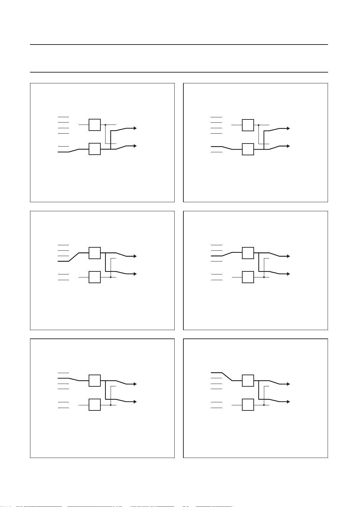
Philips Semiconductors Product specification
PAL/NTSC/SECAM video decoder with adaptive PAL/NTSC
comb filter, VBI data slicer and high performance scaler
AI24
AI23
AI22
AI21
AI12
AI11
AD2
AD1
Fig.44 Mode 0 CVBS (automatic gain)
CHROMA
LUMA
MHB559
AI24
AI23
AI22
AI21
AI12
AI11
AD2
AD1
Fig.45 Mode 1 CVBS (automatic gain).
SAA7114
CHROMA
LUMA
MHB560
AI24
AI23
AI22
AI21
AI12
AI11
AD2
AD1
Fig.46 Mode 2 CVBS (automatic gain).
AI24
AI23
AI22
AI21
AI12
AI11
AD2
AD1
CHROMA
LUMA
MHB561
CHROMA
LUMA
MHB563
AI24
AI23
AI22
AI21
AI12
AI11
AD2
AD1
Fig.47 Mode 3 CVBS (automatic gain).
AI24
AI23
AI22
AI21
AI12
AI11
AD2
AD1
CHROMA
LUMA
MHB562
CHROMA
LUMA
MHB564
Fig.48 Mode 4 CVBS (automatic gain).
2004 Mar 03 96
Fig.49 Mode 5 CVBS (automatic gain).
Page 97
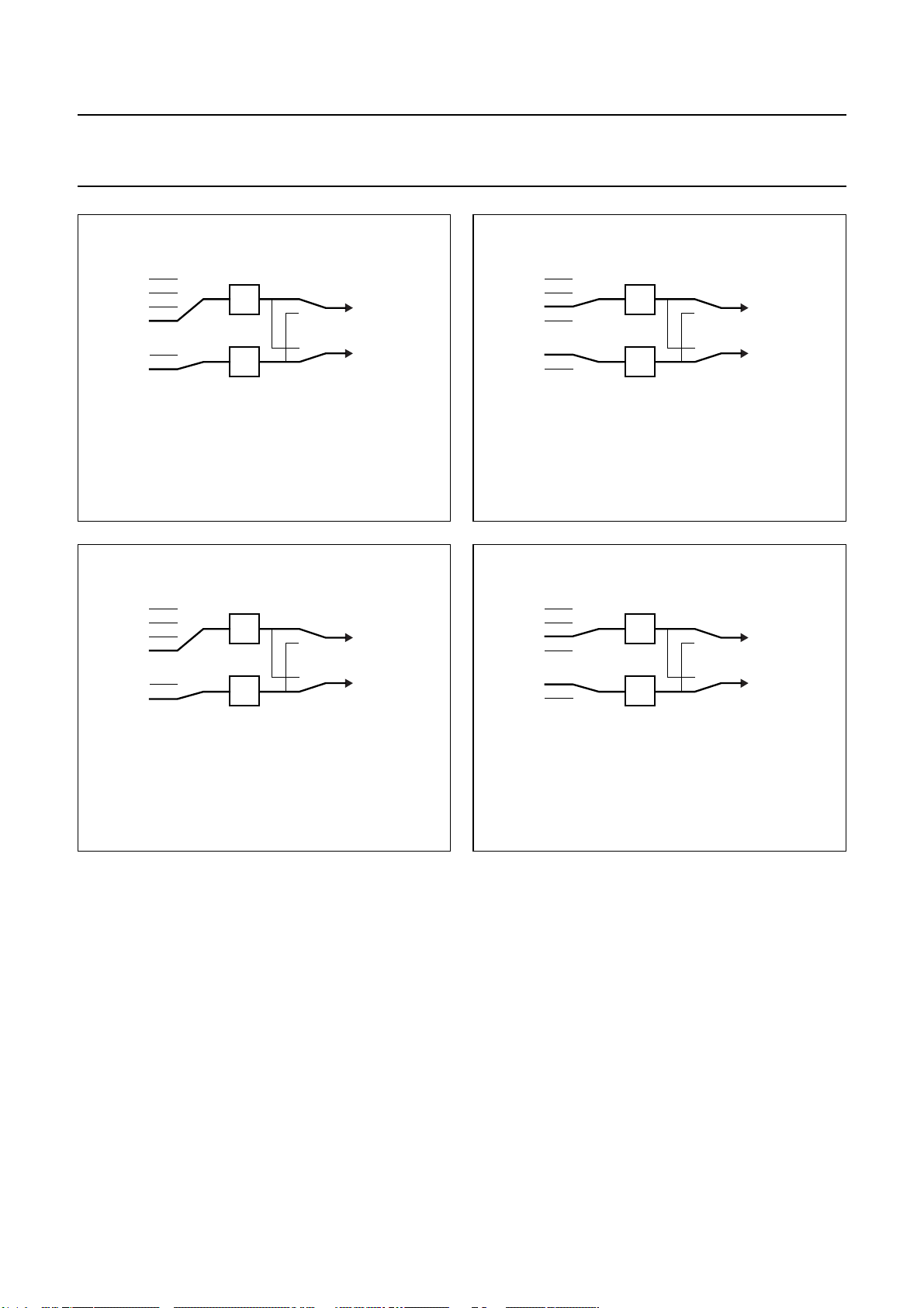
Philips Semiconductors Product specification
PAL/NTSC/SECAM video decoder with adaptive PAL/NTSC
comb filter, VBI data slicer and high performance scaler
AI24
AI23
AI22
AI21
AI12
AI11
I2C-bus bit BYPS (subaddress 09H, bit D7) should be set to logic 1
(full luminance bandwidth).
AD2
AD1
CHROMA
LUMA
MHB565
Fig.50 Mode 6 Y + C (gain channel 2 adjusted via
GAI2).
AI24
AI23
AI22
AI21
AI12
AI11
I2C-bus bit BYPS (subaddress 09H, bit D7) should be set to logic 1
(full luminance bandwidth).
AD2
AD1
Fig.51 Mode 7 Y + C (gain channel 2 adjusted via
GAI2).
SAA7114
CHROMA
LUMA
MHB566
AI24
AI23
AI22
AI21
AI12
AI11
I2C-bus bit BYPS (subaddress 09H, bit D7) should be set to logic 1
(full luminance bandwidth).
AD2
AD1
CHROMA
LUMA
MHB567
Fig.52 Mode 8 Y + C (gain channel 2 adapted to
Y gain).
AI24
AI23
AI22
AI21
AI12
AI11
I2C-bus bit BYPS (subaddress 09H, bit D7) should be set to logic 1
(full luminance bandwidth).
AD2
AD1
CHROMA
LUMA
MHB568
Fig.53 Mode 9 Y + C (gain channel 2 adapted to
Y gain).
2004 Mar 03 97
Page 98
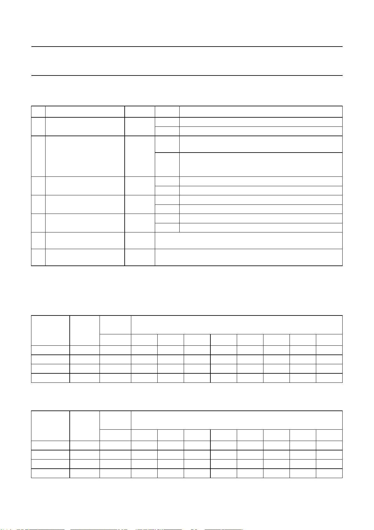
Philips Semiconductors Product specification
PAL/NTSC/SECAM video decoder with adaptive PAL/NTSC
comb filter, VBI data slicer and high performance scaler
15.2.4 SUBADDRESS 03H
Table 42 Analog input control 2 (AICO2); 03H[6:0]
BIT DESCRIPTION SYMBOL VALUE FUNCTION
D6 HL not reference select HLNRS 0 normal clamping if decoder is in unlocked state
(1)
1
reference select if decoder is in unlocked state
D5 AGC hold during vertical
blanking period
D4 white peak control off WPOFF 0
D3 automatic gain control
integration
D2 gain control fix GAFIX 0 automatic gain controlled by MODE3 to MODE0
D1 static gain control channel 2
sign bit
D0 static gain control channel 1
sign bit
VBSL 0 short vertical blanking (AGC disabled during equalization
and serration pulses)
1 long vertical blanking (AGC disabled from start of
pre-equalization pulses until start of active video (line 22 for
60 Hz, line 24 for 50 Hz)
(1)
white peak control active
1 white peak control off
HOLDG 0 AGC active
1 AGC integration hold (freeze)
1 gain is user programmable via GAI[17:10] and GAI[27:20]
GAI28 see Table 44
GAI18 see Table 43
SAA7114
Note
1. HLNRS = 1 should not be used in combination with WPOFF = 0.
15.2.5 SUBADDRESS 04H
Table 43 Analog input control 3 (AICO3): static gain control channel 1; 03H[0] and 04H[7:0]
DECIMAL
VALUE
0... −3 0 00000000
...144 0 0 1 0 0 1 0 0 0 0
145... 0 0 1 0 0 1 0 0 0 1
...511 +6 1 1 1 1 1 1 1 1 1
15.2.6 SUBADDRESS 05H
Table 44 Analog input control 4 (AICO4); static gain control channel 2; 03H[1] and 05H[7:0]
DECIMAL
VALUE
0... −3 0 00000000
...144 0 0 1 0 0 1 0 0 0 0
145... 0 0 1 0 0 1 0 0 0 1
...511 +6 1 1 1 1 1 1 1 1 1
GAIN
(dB)
GAIN
(dB)
SIGN BIT
03H[0]
GAI18 GAI17 GAI16 GAI15 GAI14 GAI13 GAI12 GAI11 GAI10
SIGN BIT
03H[1]
GAI28 GAI27 GAI26 GAI25 GAI24 GAI23 GAI22 GAI21 GAI20
CONTROL BITS D7 TO D0
CONTROL BITS D7 TO D0
2004 Mar 03 98
Page 99
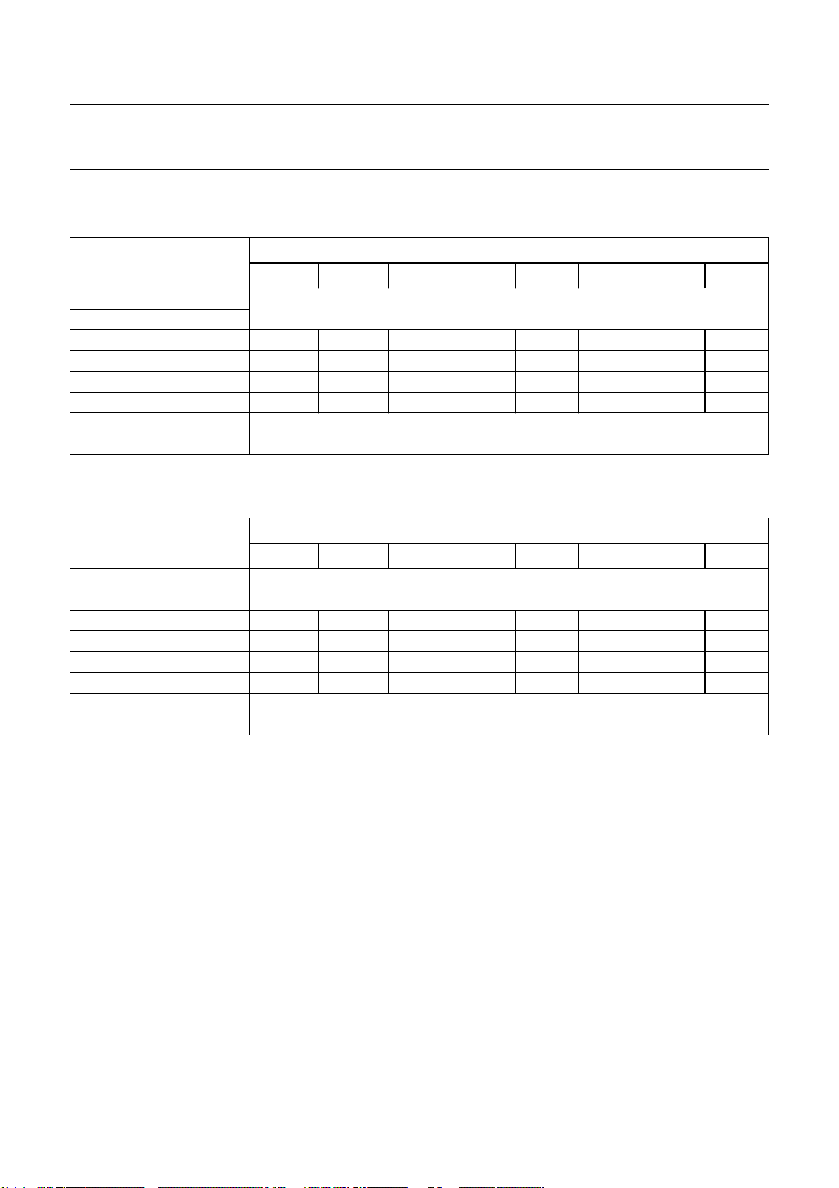
Philips Semiconductors Product specification
PAL/NTSC/SECAM video decoder with adaptive PAL/NTSC
comb filter, VBI data slicer and high performance scaler
15.2.7 SUBADDRESS 06H
Table 45 Horizontal sync start; 06H[7:0]
DELAY TIME
(STEP SIZE = 8/LLC)
−128...−109 (50 Hz) forbidden (outside available central counter range)
−128...−108 (60 Hz)
−108 (50 Hz)... 1 0 010100
−107 (60 Hz)... 1 0 010101
...108 (50 Hz) 0 1 101100
...107 (60 Hz) 0 1 101011
109...127 (50 Hz) forbidden (outside available central counter range)
108...127 (60 Hz)
15.2.8 SUBADDRESS 07H
Table 46 Horizontal sync stop; 07H[7:0]
DELAY TIME
(STEP SIZE = 8/LLC)
−128...−109 (50 Hz) forbidden (outside available central counter range)
−128...−108 (60 Hz)
−108 (50 Hz)... 1 0 010100
−107 (60 Hz)... 1 0 010101
...108 (50 Hz) 0 1 101100
...107 (60 Hz) 0 1 101011
109...127 (50 Hz) forbidden (outside available central counter range)
108...127 (60 Hz)
HSB7 HSB6 HSB5 HSB4 HSB3 HSB2 HSB1 HSB0
HSS7 HSS6 HSS5 HSS4 HSS3 HSS2 HSS1 HSS0
CONTROL BITS D7 TO D0
CONTROL BITS D7 TO D0
SAA7114
2004 Mar 03 99
Page 100
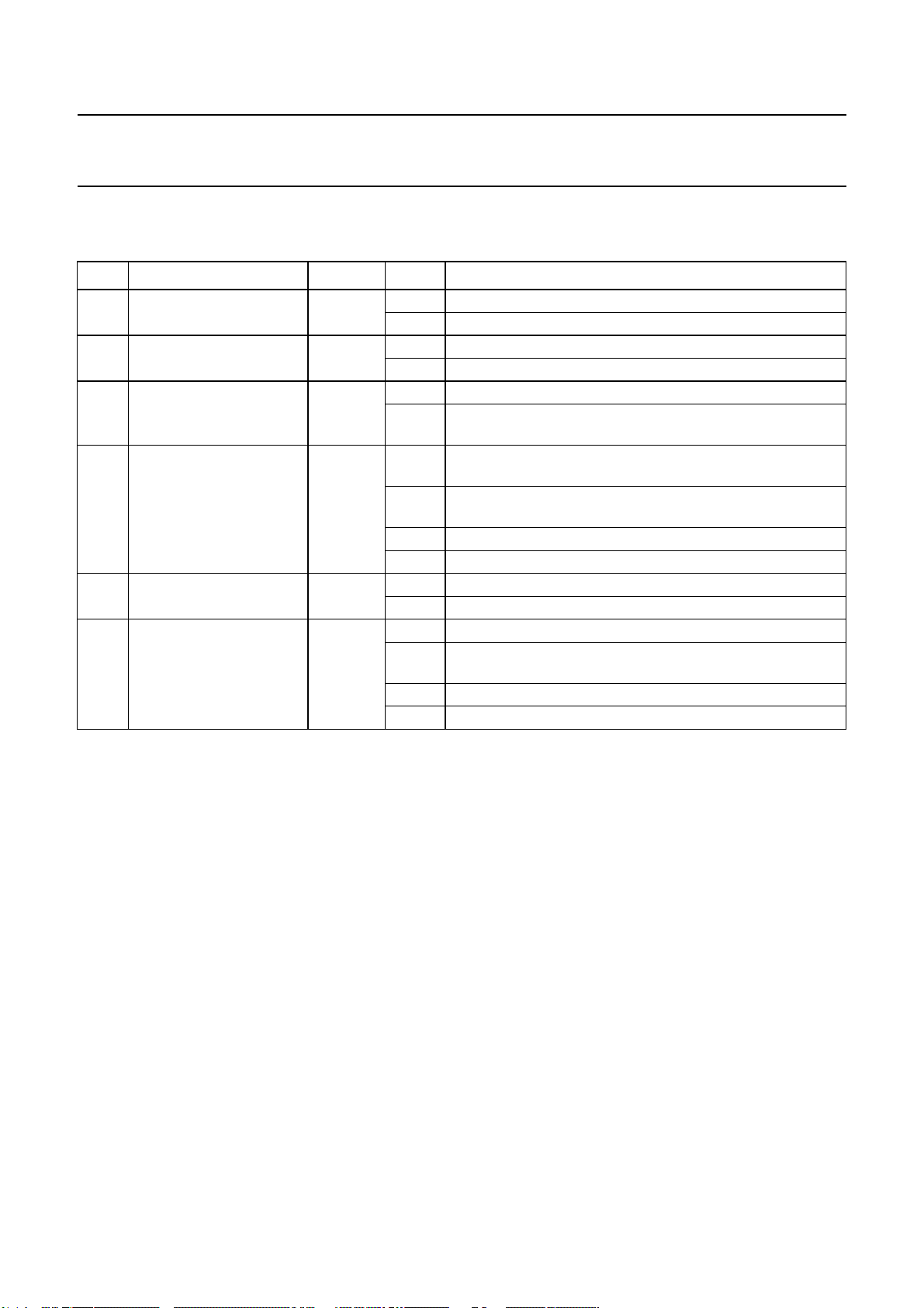
Philips Semiconductors Product specification
PAL/NTSC/SECAM video decoder with adaptive PAL/NTSC
SAA7114
comb filter, VBI data slicer and high performance scaler
15.2.9 SUBADDRESS 08H
Table 47 Sync control; 08H[7:0]
BIT DESCRIPTION SYMBOL VALUE FUNCTION
D7 automatic field detection AUFD 0 field state directly controlled via FSEL
1 automatic field detection; recommended setting
D6 field selection; active if
AUFD = 0
D5 forced ODD/EVEN toggle FOET 0 ODD/EVEN signal toggles only with interlaced source
D[4:3] horizontal time constant
selection
D2 horizontal PLL HPLL 0 PLL closed
D[1:0] vertical noise reduction VNOI[1:0] 00 normal mode; recommended setting
FSEL 0 50 Hz, 625 lines
1 60 Hz, 525 lines
1 ODD/EVEN signal toggles fieldwise even if source is
non-interlaced
HTC[1:0] 00 TV mode, recommended for poor quality TV signals only; do
not use for new applications
01 VTR mode, recommended if a deflection control circuit is
directly connected to the SAA7114
10 reserved
11 fast locking mode; recommended setting
1 PLL open; horizontal frequency fixed
01 fast mode, applicable for stable sources only; automatic field
detection (AUFD) must be disabled
10 free running mode
11 vertical noise reduction bypassed
2004 Mar 03 100
 Loading...